half-bridge drivers a transformer or an all-silicon drive?
TRANSCRIPT

Half-Bridge DriversA Transformer or an All-Silicon Drive?
Agenda• Topologies using a half-bridge configuration
• The difference between soft and hard-switching
• The gate-drive transformer
• The all-silicon-solution
• Comparison
• Conclusions

Agenda• Topologies using a half-bridge configuration
• The difference between soft and hard-switching
• The gate-drive transformer
• The all-silicon-solution
• Comparison
• Conclusions

Topology Trend for High Efficiency• Soft Switching
– LLC-HB resonant– Active clamp forward– Active clamp flyback– Asymmetrical half-bridge– Full bridge with phase shift
• Hard Switching– Flyback– Forward– 2-sw flyback– 2-sw forward– Full bridge
LLC-HB
Active clamp Forward
Active clamp Flyback
AHB
FB Phase-shift

The High-Side Switch
• To achieve high efficiency, the topologies with ZVS (Zero-Voltage Switching) behavior are preferred.
• All the soft switching topologies implement the power switch with floating reference pin, e.g. the source pin of MOSFET.
• Why are MOSFETs used in soft switching applications?– High frequency operation– Body diode (current loop for ZVS)
How to drive the high side MOSFET?

Agenda• Topologies using a half-bridge configuration
• The difference between soft and hard-switching
• The gate-drive transformer
• The all-silicon-solution
• Comparison
• Conclusions

D
G
S
Turn-on Procedure for Hard-switching
• Stages 2 and 3 dominate the switching losses of MOSFET and driver.• DRV’s source capability as VGS is around VGS,Miller is important.
CDS
CGD
CGS
RG,IRGATERHI
VDRV
IDVTH
VGS
IG
VDS
ID
VGS,Miller
S1 S2 S3 S4
IG
The Miller plateau
The miller plateau is caused by CGD
D
G
S
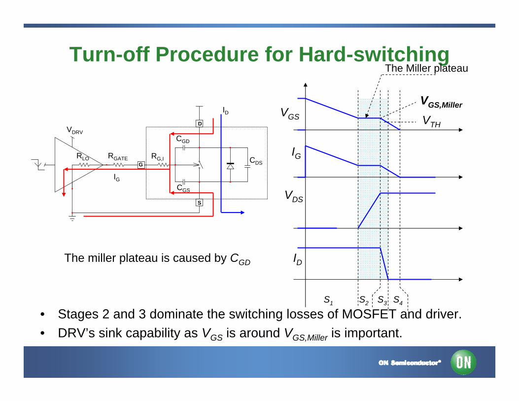
Turn-off Procedure for Hard-switching
• Stages 2 and 3 dominate the switching losses of MOSFET and driver.• DRV’s sink capability as VGS is around VGS,Miller is important.
CDS
CGD
CGS
RG,IRGATERLO
VDRV
IDVTH
VGS
IG
VDS
ID
VGS,Miller
S1 S2 S3 S4
IG
The Miller plateau
The miller plateau is caused by CGD

17
Vin250
18
D11N4148
16
Resr100m
C2440uF
Rload2.5
Vout2
1
5
Ll0.1uH
Lp1.75mH
Rp300m
Ip
RATIO_POW = -0.0667RATIO_AUX = -0.0667
7
Aux
21C510uF
22
R113.9k
C647pF
Isnub
R9300m
Iout
3
Rg15
13
Rsense1
14R131kC1
470pF
23
Vgs
Vsense
12
Verr
11
Rupper4.851k
Rlower0.97k
9
R1720k
C43.97nF
C7470pF 6 Vdrain
X1MBRS340t3 Out
Out
Vramp
CMP
FB
OSCSENS
OUT
GND
X2PWMCM
10
D3MUR160
Iclipp
Aux
R5470
Rclamp88k
Cclamp1.4nF
ΔVclipp
Vdrv
V1Ipri
D21N4148
X3IRF840
Simulation Circuit of Flyback
• Simulate the VGS, VDS, and IDS on Flyback.
IDS

0
4.00
8.00
12.0
16.0
vgs
in v
olts
plot
1
1
-100
100
300
500
700
vdra
in in
vol
tspl
ot3
2
1.01995m 1.02005m 1.02015m 1.02025m 1.02035mtime in seconds
-400m
0
400m
800m
1.20
ipri
in a
mpe
res
plot
2 3
VGS
VDS
IDS
Turn-on Simulation of Flyback
• VGS rises with Miller effect.
50 ns / div
200 mA / div
50 ns / div
200 V / div
50 ns / div
2 V / div

0
4.00
8.00
12.0
16.0
vgs
in v
olts
plot
1
1
-100
100
300
500
700
vdra
in in
vol
tspl
ot3
2
1.0244m 1.0246m 1.0248m 1.0250m 1.0252mtime in seconds
-400m
0
400m
800m
1.20
ipri
in a
mpe
res
plot
2
3
VGS
VDS
IDS
Turn-off Simulation of Flyback
• Turn off with Miller effect.
100 ns / div
200 mA / div
100 ns / div
200 V / div
100 ns / div
2 V / div

Turn-on Procedure for Soft-switching• Because of ZVS, there is no Miller
effect as turning on.
• The switching losses are dominated by– The dead time (to reduce S1), and– Source capability to charge CGS to
reduce S2
• Less driver capability requirement.
VTH
VGS
IG
VDS
ID
S1 S2 S3 ID depends on topology
-Vf

Turn-off Procedure for Soft-switching
• Similar as hard-switching: The Miller plateau exists as turning off.
• The difference is that IDS also reduces at this duration since IDS will go through the opposite MOSFET as VDS changes.
• To avoid overlap between 2 MOSFETs, minimize the duration of S1 ~ S4.
• Strong DRV’s sink capability is needed.
VTHVGS
IG
VDS
IDS
VGS,Miller
S1 S2 S3 S4
The Miller plateau

10 12Ls{Ls}
2
Lmag{Lmag}
Cs{Cs}
1
4X3XFMR-TAPRATIO = 1/N
ILmag
ICs
Vcs
ΔVLmag
26
V3{Vbulk}
23
B1Voltage
V(G2) < 2.5 ?0 :15
24
B2Voltage?
19
Mlower
Vbridge
Cs
Δ22
Mupper
* WV3
R105m
R1115
R1415
11
V4
IML
M2IRF840
5
M1IRF840
X12MBR2045
X13MBR2045
Δ
YM1
V10IM1D2
1N4148
D31N4148
Simulation Circuit of LLC-HB
• Simulate the VGS_MU, VDS_MU, and IMU on LLC-HB• To ease the reading of current, the direction of IMU and IML is referred to ICS.
IMU
ICS
IML

Turn-on Simulation of LLC-HB
• VGS_ML off, ICS reduces VDS_MU for ZVS.• VDS_MU is 0 V BEFORE VGS_MU, so VGS_MU rises smoothly.
-2.00
2.00
6.00
10.0
14.0
mlo
wer
, mup
per
in v
olts
plot
1
1
2
0
100
200
300
400
ym1
in v
olts
plot
2
3
10.1922m 10.1926m 10.1930m 10.1934m 10.1938mtime in seconds
-2.00
-1.00
0
1.00
2.00
im1,
iml i
n am
pere
spl
ot3
4
5
VGS_MUVGS_ML
VDS_MU
I_ML I_MU
Not overlap; it is the current through CDS
200 ns / div
500 mA / div
200 ns / div
200 V / div
200 ns / div
2 V / div

Turn-off Simulation of LLC-HB
• Strong turn off capability is required.
-2.00
2.00
6.00
10.0
14.0
mlo
wer
, mup
per
in v
olts
Plo
t1
2
1
0
100
200
300
400
ym1
in v
olts
Plo
t2
3
10.1976m 10.1978m 10.1980m 10.1982m 10.1984mtime in seconds
-2.00
-1.00
0
1.00
2.00
iml,
im1
in a
mpe
res
Plo
t3
45
VGS_MLVGS_MU
VDS_MU
I_MU VGS_ML100 ns / div
500 mA / div
100 ns / div
200 V / div
100 ns / div
2 V / div

Driver Comparison between Hard-Switching and Soft-Switching
AccurateAccurateDead time accuracy requirement
HighHighSink capability requirement
LowMediumSource capability requirement
Soft-switchingHard-switching

The Solutions for High-Side Driver
• Transformer-based solution
– Single DRV input
– Dual DRV inputs
• Silicon integrated circuit driver: dual outputs
– Single DRV input
– Dual DRV inputs

Agenda• Topologies using a half-bridge configuration
• The difference between soft and hard-switching
• The gate-drive transformer
• The all-silicon-solution
• Comparison
• Conclusions

Consideration as Designing Driver Transformer
• Ground-referenced floating drive – keep 500 V isolation if a 400 V pre-regulated PFC exists.
• Minimize the leakage inductance - the delay between output and input windings may kill the power MOSFETs.
• Follow Faraday’s law – keep V*T constant, otherwise, saturate.
• Keep enough margin from saturation – the worst case happens with transient load at high line.
• High permeability ferrite – minimize the IM.
• Keep high sink current capability

Single DRV Input
• An ac coupling capacitor (CC) is needed to reset the driver transformer flux.• The amplitude of VGS is dependent on duty. • With (-VC) to turn off at steady state, but the sink capability is limited at start-up. • Need a fast time constant (LM//RGS * CC) to avoid flux walking due to the fast transient.• Watch out the ringing between CC and drive transformer at skip mode or UVLO, a diode is
needed to damp the ringing.
DRV
CCRC
+ -VC
Dead time generatorDriver
C
M
C
MC C
LCL
QR 21
=≥
DRVC DVV =VDRV - VC
- VC
RGS
CC to reset the driver transformer and RC to damp the L-C resonance.
5.01=>
C
M
C CL
RQ

Single DRV Input with DC Restore
• VGS amplitude is independent on duty ratio at steady state.
• Limited sink capability.
DRV
CC1RC
+ -VC
Dead time generatorDriver
C
MC C
LR 2≥
DRVC DVV =
VDRV - Vf
- Vf
RGS
CC2
+-VC-Vf

Single DRV Input with PNP Turn-Off
• A pnp transistor + diode help to improve the switching off.
DRV
Dead time generator Driver

Don’t Forget the AND Gate
• Add the totem-pole drivers if output capability of AND gate is limited.• Is the design finished?
No, not yet. Pay attention to the ringing among CC1, CC2 and driver transformer when skip or UVLO. A diode and resistor to damp the ringing.
DRV
Dead time generator High-side Driver
CC1 CC2

Dual Polarity Symmetrical DRV Inputs
• DRVA and DRVB are opposite-polarity and symmetrical no ac coupling capacitor.• This is suitable for push-pull type circuit, e.g. LLC-HB, but NOT for asymmetrical type, e.g.
AHB or active clamp. • Pay attention to the flux of driver transformer at line/load transient.• The strong turn off capability is still needed. • Pay attention to the delay caused by the leakage inductance. minimize the leakage
inductance and use dual output windings instead of single output winding.• Extra losses caused by voltage drop on Roff.
DRVB
DriverVDRV
- VDRV
DRVA
VDRV
- Vf
Roff
Roff

The Driver Transformer• Pros
– A transformer is more robust than a die!– Less sensitivity to spurious noise and high dV/dt pulses– Cheap?
• Cons– Complicated circuits– Pay attention on extreme line/line condition & off mode ……– Pay attention on the leakage inductance and isolation– Is the sink capability strong enough?

Agenda• Topologies using a half-bridge configuration
• The difference between soft and hard-switching
• The gate-drive transformer
• The all-silicon-solution
• Comparison
• Conclusions

IN Dead Time
Vcc
Gnd
in out
Vcc
Gnd
in out
M1
M2
VBoot
Vcc
Vbulk
DRV_HI
DRV_LO
GND
GND_HI
Silicon Half Bridge Driver PrincipleIntegrated HB driver LLC converter
IN_HIVcc
Gnd
in out
Vcc
Gnd
in out
M1
M2
VBoot
Vcc
Vbulk
DRV_HI
DRV_LO
C1GND
GND_HI
IN_LO
• Principle– Single or dual inputs– High & low side driver
Single Input
Dual Inputs
Integrated HB driver

Silicon Solution, What are its Limits?
• High-side isolation – 600 V is reached within the silicon.
• Matched propagation delay between high and low side
drive – Prevents any unbalanced transformer usage.
• High side driver supply – Bootstrap supply is requested.
• Noise immunity – Negative voltage robustness of the high side driver.

Silicon Solution, High Voltage Isolation
IN_HIVcc
Gnd
in out
Vcc
Gnd
in out
M1
M2
VBoot
Vcc
Vbulk
DRV_HI
DRV_LO
GND
GND_HI
SR
QLevel Shifter
PulseTrigger
IN_LO
Floating area
• Pulse trigger: generates pulse on each edge from IN_HI input.
• Level shifter: shifts pulses from GND reference to GND_HI reference.
• SR flip flop: latches pulses information from the level shifter.
Level shifter sustains up to
600 V

IN_HIVcc
Gnd
in out
Vcc
Gnd
in out
M1
M2
VBoot
Vcc
Vbulk
DRV_HI
DRV_LO
GND
GND_HI
SR
QLevel Shifter
PulseTrigger
IN_LO Delay
Silicon Solution, Matched Propagation Delay
Delay compensation
• Delay is inserted on the fastest path: Low side driver pathto compensate: Pulse trigger + level shifter and SR flip-flop delays.

Vcc
Gnd
in out
Vcc
Gnd
in out
M1
M2
Vbulk
DRV_HI
DRV_LO
GND
Bridge
Vboot
Cboot
DbootRbootVcc
VccVcc
CVcc
Silicon Solution, High Side Driver Supply
• Bootstrap technique is used for supplying the high side driver
Bootstrap connected to VccBootstrap Step:• Step 1: M2 is closed Cboot is
grounded: Cboot is refueled via Vcc.
• Step 2: M1 & M2 are opened Bridge pin is floating, Dboot is blocked & Cboot supplies floating area.
• Step 3: M1 is closed bridge pin moved to bulk level, Dboot is still blocked & Cboot supplies floating area.

Root of High Side Driver Negative Voltage? • Let’s focus on the half-bridge branch:
– the load connected to a half-bridge branch is inductive:– like an LLC-HB– Or with the most simple case in a synchronous buck (where body
diodes of the mosfet are represented).
LLC-HB
M1
M2
Vbulk
Dbody1
Dbody2

Vbulk
Theory: Buck Converter Operation • 1st step of the buck converter:
Step 1:M1 ONM2 OFF
VBridgeTime
Time
VBridge
Step: 1
VBulk
M1 ON
M2 OFF
IL
IL

Vbulk
Theory: Buck Converter Operation• 2nd step of the buck converter:
Step 2:M1 OFFM2 OFF
VBridgeTime
Time
VBridge
Step: 1
VBulk
-Vf
2
M1 OFF
M2 OFF
IL
IL

Vbulk
Theory: Buck Converter Operation• 3rd step of the buck converter:
Step 3:M1 OFFM2 ON
VBridgeTime
Time
VBridge
Step: 1
VBulk
-Vf
2
M1 OFF
M2 ON
3
IL
IL

Vbulk
Theory: Buck Converter Operation• 4th step of the buck converter:
Step 4:M1 OFFM2 OFF
VBridgeTime
Time
VBridge
Step: 1
VBulk
-Vf
2
M1 OFF
M2 OFF
3 4 1
IL
IL

Bench: Buck Converter Operation• Anywhere but in a ppt file there are parasitic elements:
– True buck converter:
M1
M2
Vbulk
Dbody1
Dbody2
Parasiticinductances
ParasiticCapacitors

Vbulk
Bench: Buck Converter Operation• 1st step of the buck converter:
Step 1:M1 ONM2 OFF
VBridgeTime
Time
VBridge
Step: 1
VBulk
M1 ON
M2 OFF
IL
IL

Vbulk
Bench: Buck Converter Operation• 2nd step of the buck converter:
Step 2:M1 OFFM2 OFF
IL
VBridge
IL
Time
Time
VBridge
Step: 1
VBulk
-Vf
2
M1 OFF
M2 OFF
Time
1.453000ms 1.453200ms 1.453400ms1.452846msV(BRIDGE)
0V
20.0V
-10.0V
31.8V

Bench: Buck Converter Operation• 3rd step of the buck converter:
Step 3:M1 OFFM2 ON
VBridgeTime
Time
VBridge
Step: 1
VBulk
-Vf
2
M1 OFF
M2 ON
3
IL
IL
Vbulk

Vbulk
Bench: Buck Converter Operation• 4th step of the buck converter:
Step 4:M1 OFFM2 OFF
VBridgeTime
Time
VBridge
Step: 1
VBulk
-Vf
2
M1 OFF
M2 OFF
3 4 1
IL
IL

Bench: Buck Converter Operation• Negative voltage on bridge pin will create negative current
injection inside the IC driver.
IN_HI
Vcc
Gnd
in out
M1
M2
VBoot
Vcc
Vbulk
DRV_HI
DRV_LO
GND
Bridge
SR
QLevel Shifter
PulseTrigger
IN_LO Delay
Vcc
Gnd
in out VBridge
Floating area
Leaky path when VBridge < 0VThis leakage path could create some trouble inside the driver IC.

How to Characterize the Negative Voltage?
Time
VBridge
VBulk
-Vf
Time
VBridge
Width
Principle:
Negative pulse is added on bridge pin:
With adjustable Negative voltage
And adjustable Width
Vneg
At each pulse width the neg. voltage is increased until the driver IC fails.
How the Negative Voltage has Been Created?
L1
100uHIN_LO
IN_HI
C710uF25V
C19100nF
C3220uF50V
D13D1N4148
Rload10R
0Pulse gen.
0
VCC
D14D1N4148
TX1
BZX84C18D5
BZX84C18D6
C13
100n
Q4FDP3682
Q5FDP3682
Q6FDP3682
VCC
Vout
BZX84C18D7R10
47k
0
C4330uF100V
C12100nF
Rload110R
VDC_IN20V
D11D1N4148
U1NCP5106A
VCC1
IN_HI2
IN_LO3
GND4
DRV_LO5
BRIDGE6
DRV_HI7
VBOOT8
0
0R11R
R2
10RQ1Q2N2907
R3
10R
Q2Q2N2907
Vneg
0Vdc to 50V
D4
MBR1100
R4
10R C11100n
U5MC33152
1 2
Sync
R847k
R947k
Synchronous Buck
Converter
Negative pulse generation
IC Driver
Adj. VNeg
Adj. pulse width

Example of Negative Voltage MeasurementVG_LO
(10 V/div)
VG_HI
(10 V/div)
Vbridge pin
(20 V/div)
Time
(80 ns/div)Width = 150 ns
Vneg = -18 V
When the bridge pin is released, it generates some noise on the hi-
side driver.
Note: Negative voltage pulse is applied when the bridge pin voltage is reaching zero.

Negative Voltage versus Neg. pulse duration @ +25°C
-35
-30
-25
-20
-15
-10
-5
00 100 200 300 400 500 600
Negative pulse duration (ns)
Nega
tive
puls
e vo
ltage
(V
)
Negative Voltage Characterization
If the negative pulse is inside this area, the driver will not work properly or can be damaged.
If the negative pulse is inside this area, the driver will work properly.

Negative Voltage Characterization in Temperature
Negative Voltage versus Neg. pulse duration @ different Temp
-35
-30-25
-20
-15
-10-5
00 100 200 300 400 500 600
Negative pulse duration (ns)
Nega
tive
puls
e vo
ltage
(V
)
-40°C25°C125°C
• Note: These characterizations will be available in each IC driver datasheet

Driver IC Remarks• ON Semiconductor defines electrical parameters on overall
temperature range (here -40℃ < Tj < +125 ℃). See electrical table & characterization curves.
• Competitors define the electrical parameters only at Tamb = +25℃. Temp characterization is not always available
what about min & max over extended temperature range?
• The competitors values extracted from the curves probably do not take into account the lot to lot process variations
the range variation is probably wider.

ON Semiconductor IC Driver Cross Reference
•3.3 V CMOS/TTL input•Internal fixed dead time 650 ns•One pin for creepage
IR2111 –IRS2111, NA30 ns / 60 ns
750 ns / 100 ns
85 ns /35 ns
NCP5111
•3.3 V CMOS/TTL input•Internal fixed dead time 520 nsIR2104 –
IRS2104NA10 ns /45 ns620 ns /100 ns
85 ns /35 ns
NCP5104
•3.3 V CMOS/TTL inputs•Internal fixed dead time 100 ns
IR2304 -IRS2304, L6388/84FAN7380
20 ns / 35 ns100 ns / 100 ns
85 ns /35 ns
NCP5304
•3.3 V CMOS/TTL inputs•Internal fixed dead time 100 ns
IR2106 –IRS2106,FAN7382
20 ns / 35 ns100 ns / 100 ns
85 ns /35 ns
NCP5106B
•3.3 V CMOS/TTL inputsIR2106 –IRS2106,FAN7382
-20 ns / 35 ns100 ns / 100 ns
85 ns /35 ns
NCP5106A
•3.3 V CMOS/TTL inputsIR2181 –IRS2181-20 ns / 35 ns
100 ns / 100 ns
40 ns / 20 ns
NCP5181
RemarksPin-Out
Compati-bility
Cross Conduction Protection
Matching Delay
Typ / Max
Propag.Delay typ.tON / tOFF
Drive trise / tfall typ.
(CL=1 nF)

Agenda• Topologies using a half-bridge configuration
• The difference between soft and hard-switching
• The gate-drive transformer
• The all-silicon-solution
• Comparison
• Conclusions

3 26
L1
5
4
8
T1XFMR
C1
C3a1mF
7
C8100p
R1410k
15R15
D41N4148
17
28
M1IRFB11N50A
24
M2IRFB11N50A
40
16U2TL431
13
R610k
out
R786k
R810k
C5470p
L34.7uH
C2680uFPart number = EEUFC1V681
int out
int
10
R122k
C410n
R222k
18
C6470p
R322k
C7 C10
+400 V
0 V
R547k
R947k
45
11
2
30 12
42 14
41
19
23
1
2
3
4
5
8
6
7
9
10
11
12
13
14
15
1629
37
38
39
6
1
31
NCP1395A
timer
BO
analog ground
C15100n
C1822u
R16
R24 250k
75k
R11 160k
C19 10u
R12 150k
C20 10u
R19 5.2k
10nC14
C13
U5ASFH615-A
C1110n
R224.7k
R251.8Meg
100n
540
R2310k
U5BSFH615-A
Vcc
InA
InB
Gnd
OutA
OutB
VB
Gnd
C3b1mF
C3c1mFPart number = EEUFC1V102
Irms=5 A24 V / 10 AP = 4W
22nFPart number = PHE450MB5220JR06
C1
0.47uFPart number = PHE450MF6470JR06L2C7
100uFPart number = 2222-05737101C10Snap-in BC Comp. 450 V
EVOX RIFA 630 V
EVOX RIFA 630 V
D3mbr1645
D6mbr1645
D11mbr1645
D12mbr1645
Heatsink 18°C/WKL112-25
L1PCV-0-274-04220u
1 kV
PCV-0-472-20L
ETD44ET4415A
KL195/25,4SW
KL195/25,4SW
R3233k
R335.6k
FF
FF
20
21
25
22
T2Q3903-A
D151n5818
D171n5818
..
Vcc
D51n5818
D71n5818
R171k
R181k
27
D101N4148
R2010
32R211k
33
R41k
34
D81N4148 R10
10
.
Vcc
C1610u
C170.1u
R30
47k
R2947k
1
6
2
5
3
4
Q12N2222
Q52N2907
Q22N2222
Q62N2907
Q102N2907
Q112N2907
LLC-HB Schematic with Driver Transformer
• LLC-HB with 24 V @ 10 A• NCP1395, the LLC controller with dual DRV outputs.• Transformer drivers the MOSFETs of LLC converter.
Driver Transformer
LLC controller
NCP1395

3 26
L1
5
4
8
T1XFMR
C1
C3a1mF
7
C8100p
R1410k
15R15
D41N4148
17
28
M1IRFB11N50A
24
M2IRFB11N50A
40
16U2TL431
13
R610k
out
R786k
R810k
C5470p
L34.7uH
C2680uFPart number = EEUFC1V681
int out
int
10
R122k
C410n
R222k
18
C6470p
R322k
C7 C10
+400 V
0 V
R547k
R947k
45
11
2
30 12
42 14
41 35
23
1
2
3
4
5
8
6
7
9
10
11
12
13
14
15
1629
37
38
39
6
1
31
NCP1395A
timer
BO
analog ground
C15100n
C1822u
R16
R24 250k
75k
R11 160k
C19 10u
R12 150k
C20 10u
R19 5.2k
10nC14
C13
U5ASFH615-A
C1110n
R224.7k
R251.8Meg
100n
540
R2310k
U5BSFH615-A
Vcc
InA
InB
Gnd
OutA
OutB
VB
Gnd
C3b1mF
C3c1mFPart number = EEUFC1V102
Irms=5 A24 V / 10 AP = 4W
22nFPart number = PHE450MB5220JR06
C1
0.47uFPart number = PHE450MF6470JR06L2C7
100uFPart number = 2222-05737101C10Snap-in BC Comp. 450 V
EVOX RIFA 630 V
EVOX RIFA 630 V
D3mbr1645
D6mbr1645
D11mbr1645
D12mbr1645
Heatsink 18°C/WKL112-25
L1PCV-0-274-04220u
1 kV
PCV-0-472-20L
ETD44ET4415A
KL195/25,4SW
KL195/25,4SW
R3233k
R335.6k
FF
FF
1
2
3
4 5
8
6
7
51
44
36
U1NCP5181
25
D11N4937
R1310
C9100nF
R2610
R2710
C12100n
D21N4148
D91N4148
R2847k
R3147k
LLC-HB Schematic with Driver IC
• LLC-HB with 24 V @ 10 A• NCP1395, the LLC controller with dual DRV outputs.• NCP5181, driver IC drives the MOSFETs of LLC converter.
LLC controller
NCP1395
Driver IC
NCP5181

VGS Waveform
• The waveforms seem similar.
Driver transformer Driver IC (NCP5181)
VGS_ML
(5 V/div)
VGS_MU
(5 V/div)IMU(2 A/div)
VDS_ML
(100 V/div)
2 µs / div
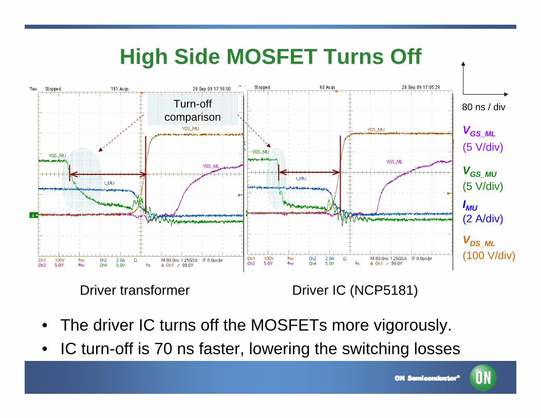
High Side MOSFET Turns Off
• The driver IC turns off the MOSFETs more vigorously.• IC turn-off is 70 ns faster, lowering the switching losses
Turn-off comparison
80 ns / div
Driver transformer Driver IC (NCP5181)
VGS_ML
(5 V/div)
VGS_MU
(5 V/div)IMU(2 A/div)
VDS_ML
(100 V/div)

High side MOSFET Turns On
• The driver IC keeps safe and enough dead time between high and low side MOSFETs.
200 ns / divTurn-on
comparison
Driver transformer Driver IC (NCP5181)
VGS_ML
(5 V/div)
VGS_MU
(5 V/div)IMU(2 A/div)
VDS_ML
(100 V/div)

The Efficiency Comparison
• There is no efficiency difference between the IC driver and transformer solutions.
Input power (W)
Output power (W)
Vout(V)
Iout(A) η
128.33 119.72 23.96 5.00 93.29%257.2 235.46 23.57 9.99 91.55%
128.34 119.72 23.96 5.00 93.29%258.5 236.46 23.67 9.99 91.48%
Driver Transformer
Driver IC

Agenda• Topologies using a half-bridge configuration
• The difference between soft and hard-switching
• The gate-drive transformer
• The all-silicon-solution
• Comparison
• Conclusions

Conclusion: Transformer or IC?• Both solutions work if well-trimmed.
• We recommend the IC solution because:
– We don’t sell the transformer.
– Manual insertion for the transformer.
– Ease the layout
– Ease the design
– Free of transformer problems, e.g.:• isolation is destroyed,• flux walking away,• unexpected ringing after turn off,• Height of the transformer in low profile PSU

For More Information
• View the extensive portfolio of power management products from ON Semiconductor at www.onsemi.com
• View reference designs, design notes, and other material supporting the design of highly efficient power supplies at www.onsemi.com/powersupplies