handbook formula book - engineers institute · handbook & formula book for gate, ies, jto,...
TRANSCRIPT


HANDBOOK&
FORMULA BOOKfor
GATE, IES, JTO, PSU’s & SSC
ELECTRONICSENGINEERING
Published by Engineers Institute of India
2017 By Engineers Institute of India
ALL RIGHTS RESERVED. No part of this work covered by the copyrightherein may be reproduced, transmitted, stored or used in any form or by anymeans graphic, electronic, or mechanical & chemical, including but notlimited to photocopying, recording, scanning, digitizing, taping, Webdistribution, information networks, or information storage and retrievalsystems.
Engineers Institute of India
28-B/7, Jia Sarai, Near IIT Hauz Khas New Delhi-110016
Tel: 011-26514888
For publication information, visit www.engineersinstitute.com/publication
ISBN: 978-93-5156-854-4
Price: Rs. 349/-
A WORD TO THE STUDENTS

GATE and Engineering Services Examinations are themost prestigious competitive examinations conductedfor graduate engineers. Over the past few years, theyhave become more competitive as more and morenumbers of aspirants are increasingly becominginterested in post graduate qualifications &government jobs for a secured and bright career.This Formula Book consists of well-illustrated concepts, importantformulae and diagrams, which will be highly beneficial at the last leg ofcandidate’s preparation.It includes all the subjects of Electronics Engineering, which arerequired for all type of competitive examinations. Adequate emphasishas been laid down to all the major topics in the form of Tips / Notes,which will be highly lucrative for objective and short answer typequestions.Proper strategy and revision is a mandatory requirement for clearingany competitive examination. This book covers short notes andformulae for Electronics Engineering. This book will help in quickrevision before the GATE, IES & all other PSUs.This book has been designed after considering the current demand ofexaminations.It would be very fruitful if the students go through this book every day.We are presenting this book by considering all the facts which isrequired to get success in the competition.With best wishes for future career
R. K. RajeshDirectorEngineers Institute of [email protected]

This book is dedicated to all
Electronics Engineers
Preparing for GATE, IES, JTO, SSC
& Public sector examinations.

CONTENTS
1. NETWORK THEORY .............................................. 01-40
2. CONTROL SYSTEMS.............................................. 41-74
3. DIGITAL ELECTRONICS AND CIRCUITS .............. 75-118
4. MICROPROCESSORS ............................................ 119-136
5. ELECTRONIC DEVICES & CIRCUITS .................... 137-168
6. ANALOG ELECTRONICS ...................................... 169-204
7. SIGNALS AND SYSTEMS ..................................... 205-230
8. COMMUNICATION SYSTEMS ............................... 231-264
9. ELECTROMAGNETIC THEORY ............................. 265-286
10. MEASUREMENTS AND INSTRUMENTATION ....... 287-308
11. MATERIALS SCIENCE .......................................... 309-322
12. COMPUTER ORGANIZATION ………………………… 323-336
13. MICROWAVES …………………………………………….. 337-364

Why IES?Indian Engineering Services (IES) constitute of engineers that work under thegovt. of India to manage a large segment of public sector economy whichconstitutes of Railroads, Public works, Power, Telecommunications, etc. IESremain the most sought-after careers for the engineering graduates in India. Acombined competitive examination is conducted by UPSC for recruitment tothe Indian Engineering Services. The exam constitutes of a written examfollowed by an interview for personality test.Why GATE?In the present competitive scenario, where there is mushrooming ofuniversities and engineering colleges, the only yardstick to measure and testthe calibre of engineering students is the GATE.The GATE AdvantageMany public sector undertakings such as BHEL, IOCL, NTPC, BPCL, HPCL, BARCand many more PSUs are using the GATE score for selecting candidates fortheir organizations. Students who qualify in GATE are entitled to a stipend ofRs 8,000 per month during their M.Tech. course. Better remuneration is beingoffered for students of M.Tech./ME as compared to those pursuing B.Tech/B.E.A good rank assures a good job. After joining M.Tech. at IITs and IISc, one canlook at a salary package ranging from Rs 7lakh to 30lakh per annum dependingupon specialization and performance. Qualifying GATE with good marks is alsoan eligibility clause for the award of JRF in CSIR Laboratories.

ECE FORMULA BOOK 1. NETWORK THEORY [1]
Published by: ENGINEERS INSTITUTE OF INDIA. ALL RIGHTS RESERVED www.engineersinstitute.com
1NETWORK THEORY
CONTENTS1. NETWORK BASICS ………………………………………………. 02-05
2. METHODS OF ANALYSIS AND THEOREMS …………….. 06-10
3. AC FUNDAMENTALS AND R, L, C CIRCUITS ………….. 11-15
4. RESONANCE ………………………………………………………. 16-18
5. TRANSIENTS ……………………………………………………… 19-22
6. GRAPH THEORY …………………………………………………. 23-26
7. TWO PORT NETWORKS ………………………………………. 27-30
8. MAGNETIC COUPLED CIRCUITS ………………………….. 31-32
9. FILTERS ……………………………………………………………. 33-36
10. NETWORK SYNTHESIS ………………………………………. 37-40

ECE FORMULA BOOK 1. NETWORK THEORY [2]
Published by: ENGINEERS INSTITUTE OF INDIA. ALL RIGHTS RESERVED www.engineersinstitute.com
1. NETWORK BASICSCurrent: Electric current is the time rate of change of charge flow.
(Ampere)
Charge transferred between time and to
t
t
q idt Sign Convention: A negative current of –5A flowing in one direction is same as acurrent of +5A in opposite direction.Voltage: Voltage or potential difference is the energy required to move a unitcharge through an element, measured in volts.
Power: It is time rate of expending or absorbing energy.
Law of conservation of energy must be obeyed in any electric circuit. Algebraic sum of power in a circuit, at any instant of time, must be zero.
i.e. P = 0Circuit Elements:Resistor: Linear and bilateral (conduct from both direction)In time domain V(t) = I(t)RIn s domain V(s) = RI(s)
ρR= ohm
A
l
l = length of conductor, = resistivity, A = area of cross section
Extension of wire to n times results in increase in resistance: 2'R n R
dqi
dt
ot

ECE FORMULA BOOK 1. NETWORK THEORY [3]
Published by: ENGINEERS INSTITUTE OF INDIA. ALL RIGHTS RESERVED www.engineersinstitute.com
Compression of wire results in decrease in resistance: 2'R
Rn
Capacitor: All capacitors are linear and bilateral, except electrolytic capacitorwhich is unilateral.
Time Domain:Cdv(t)
i(t)=dt
t1v(t) i(t)dt
C
In s-domain: I(s) = sCV(s)1
V(s) = I(s)sC
Capacitor doesn’t allow sudden change of voltage, until impulse of current isapplied.
It stores energy in the form of electric field and power dissipation in idealcapacitor is zero.
Impedance c c c c1
Z =-jX & X = ; XωC
Capacitive reactance ; = 2f
Inductor: Linear and Bilateral element
Time Domain:( ) 1
( ) ( ) ( )t
di tv t L i t v t dt
dt L
Impedance &L L LZ jX X L
In s-domain V(s) = sL I(s)1
I(s) = V(s)sL
Inductor doesn’t allowed sudden change of current, until impulse of voltage isapplied.
It stores energy in the form of magnetic field. Power dissipation in ideal inductor is zero.
Transformer: 4 terminal or 2-port devices.
: Step down transformer : Step up transformer
1 1
2 2
V N
V N 1 2
2 1
I N
I N
Where 1
2
.N
K Turns ratioN
V1 N1 N2 V2
I2
+
–
Inputport
Outputport
I1
+
–
1 2N N 2 1N N

ECE FORMULA BOOK 1. NETWORK THEORY [4]
Published by: ENGINEERS INSTITUTE OF INDIA. ALL RIGHTS RESERVED www.engineersinstitute.com
Transformer doesn’t work as amplifier because current decreases in same amountpower remain constant.
Gyrator:
Coefficient of Gyrator
If load is capacitive then input impedance will be inductive and vice versa. If load is inductive then input impedance will be capacitive. It is used for simulation of equivalent value of inductance.
Voltage Source:
In practical voltage source, there is small internal resistance, so voltage across theelement varies with respect to current.
Ideal voltmeter, RV (Internal resistance)
Current Source:
In practical current source, there is small internal resistance, so current varies withrespect to the voltage across element.
V1
Ro
V2
I2I1
Ro
1 2V R Io 2 1V R Io

ECE FORMULA BOOK 1. NETWORK THEORY [5]
Published by: ENGINEERS INSTITUTE OF INDIA. ALL RIGHTS RESERVED www.engineersinstitute.com
Ideal Ammeter, Ra 0 (Internal resistance)
Dependent and Independent Source:Independent Source: Voltage or current source whose values doesn’t depend onany other parameters. E.g. Generator etc.
Dependent Source: Voltage or current source whose values depend upon otherparameters like current, voltage.The handling of independent and dependent voltage source is identical except.
(i) In Thevenin and Norton Theorem (ii) Superposition TheoremWhere, (i) All independent voltage sources are short circuited.
(ii) All independent current sources are open circuited.(iii) All dependent voltage and current sources are left as they are.
A network in which all network elements are physically separable is known aslumped network.
A network in which the circuit elements like resistance, inductance etc, are notphysically separate for analysis purpose, is called distributed network. E.g.Transmission line.
If an element is capable of delivering energy independently, then it is calledactive element.Example: Voltage source, Current source
If it is not capable of delivering energy, then it is passive element.Example: Resistor, Inductor, Capacitor
If voltage and current across an element are related to each other through aconstant coefficient then the element is called as linear element otherwise it iscalled as non-linear.
When elements characteristics are independent of direction of current thenelement is called bi-directional element otherwise it is called as unidirectional.Ex: R, L & C.
Diode is a unidirectional element. Voltage and current sources are also unidirectional elements. Every linear element should obey the bi-directional property but vice versa as is
not necessary. Internal resistance of voltage source is in series with the source. Internal
resistance of ideal voltage source is zero. Internal resistance of current source is in parellel with the source. Internal
resistance of ideal current source is infinite.

ECE FORMULA BOOK 1. NETWORK THEORY [6]
Published by: ENGINEERS INSTITUTE OF INDIA. ALL RIGHTS RESERVED www.engineersinstitute.com
2. METHODS OF ANALYSIS AND THEOREMS(i) Kirchoff’s Points Law or Current Law (KCL): In any electrical network, thealgebric sum of the currents meeting at point (or junction) is zero.
Incoming current = Outgoing current
I1+I2 = I3+I4
It is based on conservation of charge.
(ii) Kirchoff’s Mesh Law or Voltage Law (KVL): The algebraic sum of productsof currents and resistance in each of conductor in any closed path in a network plusthe algebraic sum of emf in that path is zero.
i.e.It is based on conservation of energy.
Determination of Voltage Sign(a) Sign of Battery E.M.F.:
(b) Sign of IR Drop:
Resistors in Series: eq 1 2 3 nR = R + R + R +...... R
Resistors in Parallel:n
1.....+
R
Inductors in Series: eq 1 2 3 nL = L + L + L ....... L
Inductors in Parallel:eq 1 2 3 n
1 1 1 1 1= + + +......
L L L L L
Capacitors in Series:eq 1 2 3 n
1 1 1 1 1= + + +......
C C C C C
Capacitor in Parallel: eq 1 2 3 nC = C + C + C +...... C
IR emf 0
eq 1 2 3
1 1 1 1
R R R R
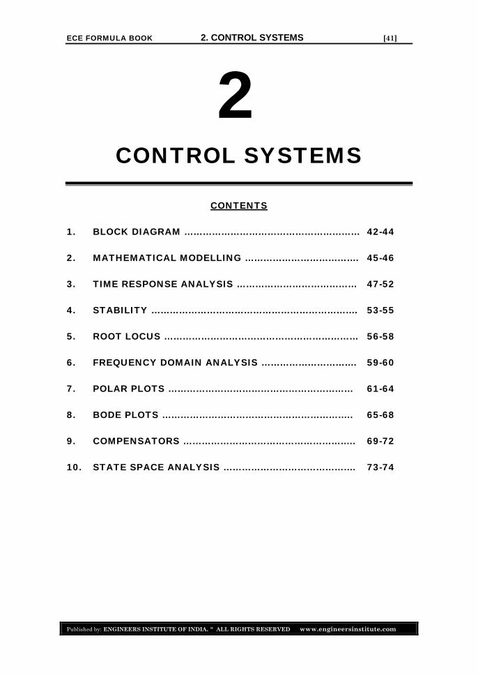
ECE FORMULA BOOK 2. CONTROL SYSTEMS [41]
Published by: ENGINEERS INSTITUTE OF INDIA. ALL RIGHTS RESERVED www.engineersinstitute.com
2CONTROL SYSTEMS
CONTENTS
1. BLOCK DIAGRAM ………………………………………………… 42-44
2. MATHEMATICAL MODELLING ………………………………. 45-46
3. TIME RESPONSE ANALYSIS ………………………………… 47-52
4. STABILITY …………………………………………………………. 53-55
5. ROOT LOCUS ……………………………………………………… 56-58
6. FREQUENCY DOMAIN ANALYSIS …………………………. 59-60
7. POLAR PLOTS …………………………………………………… 61-64
8. BODE PLOTS …………………………………………………….. 65-68
9. COMPENSATORS ……………………………………………….. 69-72
10. STATE SPACE ANALYSIS ……………………………………. 73-74

ECE FORMULA BOOK 2. CONTROL SYSTEMS [42]
Published by: ENGINEERS INSTITUTE OF INDIA. ALL RIGHTS RESERVED www.engineersinstitute.com
1. BLOCK DIAGRAMOpen Loop Control System: In this system the output is not fedback for comparison with the input.
Open loop system faithfulness depends upon the accuracy of input calibration.
When a designer designs, he simply design open loop system.Closed Loop Control System: It is also termed as feedback control system. Herethe output has an effect on control action through a feedback. Ex. Human beingTransfer Function:
C(s) G(s)Transfer function =
R(s) 1 + G(s)H(s)
Comparison of Open Loop and Closed Loop control systems:Open Loop:1. Accuracy of an open loop system is defined by the calibration of input.2. Open loop system is simple to construct and cheap.3. Open loop systems are generally stable.4. Operation of this system is affected due to presence of non-linearity in its
elements.
Closed Loop:1. As the error between the reference input and the output is continuously
measured through feedback. The closed system works more accurately.2. Closed loop systems is complicated to construct and it is costly.3. It becomes unstable under certain conditions.4. In terms of performance the closed loop system adjusts to the effects of non-
linearity present.
Transfer Function: The transfer function of an LTI system may be defined as theratio of Laplace transform of output to Laplace transform of input under theassumption
Y(s)G(s)=
X(s)
The transfer function is completely specified in terms of its poles and zeros andthe gain factor.
ECE FORMULA BOOK 2. CONTROL SYSTEMS [43]
Published by: ENGINEERS INSTITUTE OF INDIA. ALL RIGHTS RESERVED www.engineersinstitute.com
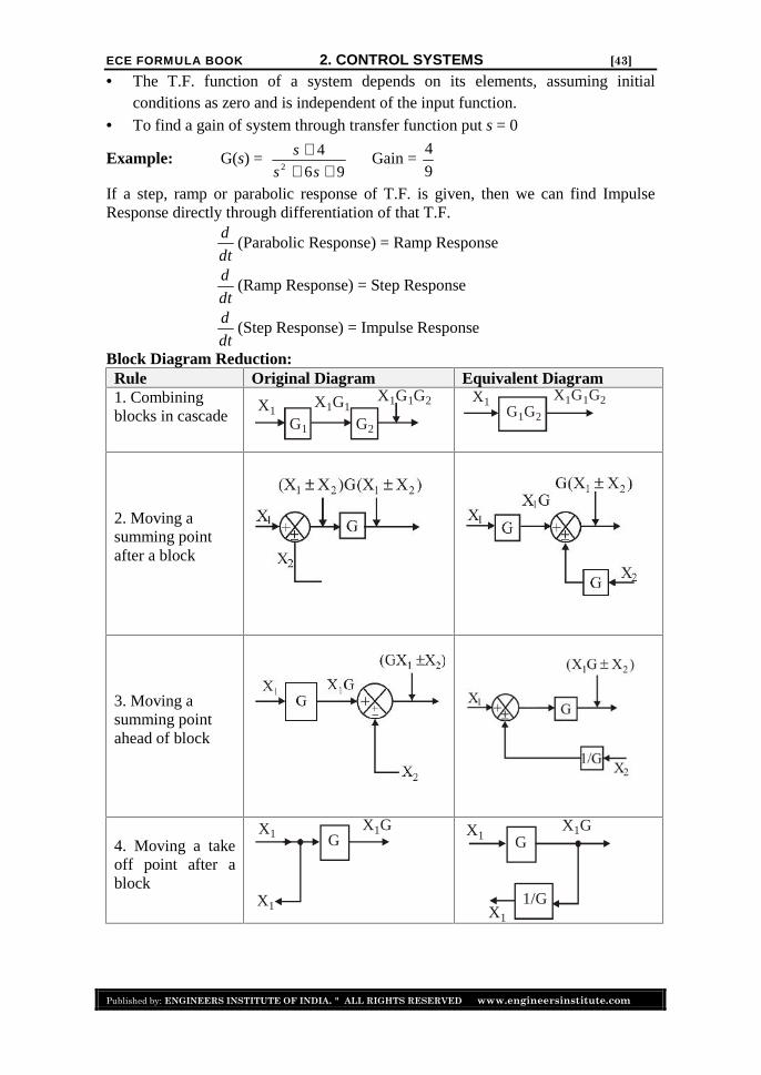
The T.F. function of a system depends on its elements, assuming initialconditions as zero and is independent of the input function.
To find a gain of system through transfer function put s = 0
Example: G(s) = Gain =
If a step, ramp or parabolic response of T.F. is given, then we can find ImpulseResponse directly through differentiation of that T.F.
(Parabolic Response) = Ramp Response
(Ramp Response) = Step Response
(Step Response) = Impulse Response
Block Diagram Reduction:Rule Original Diagram Equivalent Diagram1. Combiningblocks in cascade
2. Moving asumming pointafter a block
3. Moving asumming pointahead of block
4. Moving a takeoff point after ablock
2
4
6 9
s
s s
4
9
d
dtd
dtd
dt
G1
X1G2
X G11X G G21 1 X1
G G21
X G G21 1
GX1
X1
X G1G
X1
X1
1/G
X G1

ECE FORMULA BOOK 2. CONTROL SYSTEMS [44]
Published by: ENGINEERS INSTITUTE OF INDIA. ALL RIGHTS RESERVED www.engineersinstitute.com
5. Moving a takeoff point ahead ofa block
6. Eliminating afeedback loop
1 2(GX ± X )Signal Flow Graphs: It is a graphical representation of control system.
Signal Flow Graph of Block Diagram:
Mason’s Gain Formula: Transfer function =
Path gain of forward path
1 – [Sum of all individual loops] + [Sum of gain products of two non-touchingloops] – [Sum of gain products of 3 non-touching loops] + ………..
Value of obtained by removing all the loops touching forward path aswell as non-touching to each other
GX1 X G1
X G1
GX1
G
X G1
X G1
X1 G
1 GH
X2
k kp
kp thk
k thk

ECE FORMULA BOOK 2. CONTROL SYSTEMS [45]
Published by: ENGINEERS INSTITUTE OF INDIA. ALL RIGHTS RESERVED www.engineersinstitute.com
2. MATHEMATICAL MODELLINGMechanical System:Translational System:Mass:
F = Force on block m x = Displacement of blockV = Velocity of Block m = Mass of blockDamper Spring
by hooke’s law
Spring constant
Rotational SystemInertia
Damper Spring twisted:
2
2F
d x dvm m
dt dt
x2x1
v1 v2
K
1 2F ( )d
f x xdt
1 2 1 2F ( ) ( )k x x k v v dt k
2
1 22T ( )
df f
dt
T k k dt
2
2T J J
d d
dt dt

ECE FORMULA BOOK 2. CONTROL SYSTEMS [46]
Published by: ENGINEERS INSTITUTE OF INDIA. ALL RIGHTS RESERVED www.engineersinstitute.com
Force Voltage and Force Current Analogy:
Voltage(Series RLC)
Current(Parallel RLC)
Force(Translational)
Torque(Rotational)
V I F Tq x
R f (Damper) f (Damper)
k k
L C M JI V Linear velocity Angular velocity
Conversion of Translational System to other Systems:
2
2
d x dxF M f kx
dt dt
Force–Current Analogy:
2
2
d 1 di C
dt R dt Ldv v 1
i C + + vdtdt R L
Force–Voltage Analogy:
2
2
d q dq qV L R
dt Cdt
di 1V L iR idt
dt C
1
R
1
C
1
L

ECE FORMULA BOOK 3. DIGITAL ELECTRONICS AND CIRCUITS [75]
Published by: ENGINEERS INSTITUTE OF INDIA. ALL RIGHTS RESERVED www.engineersinstitute.com
3DIGITAL ELECTRONICS
AND CIRCUITSCONTENTS
1. NUMBER SYSTEM & CODES …………………………………. 76-78
2. BINARY AIRTHMETIC ………………………………………….. 79-82
3. LOGIC GATES …………………………………………………….. 83-89
4. DIGITAL LOGIC CIRCUITS ……………………………………. 90-95
5. SEQUENTIAL CIRCUITS ………………………………………. 96-100
6. SHIFT REGISTERS ……………………………………………… 101-102
7. COUNTERS ………………………………………………………… 103-105
8. DIGITAL LOGIC FAMILY ……………………………………… 106-112
9. ADCs AND DACs ……………………………………………… 113-116
10. MEMORIES ……………………………………………………….. 117-118

ECE FORMULA BOOK 3. DIGITAL ELECTRONICS AND CIRCUITS [76]
Published by: ENGINEERS INSTITUTE OF INDIA. ALL RIGHTS RESERVED www.engineersinstitute.com
1. NUMBER SYSTEM & CODESNumber System and Codes:
A number system with base ‘r’, contents ‘r’ different digits and they are from 0 tor – 1.Decimal to other codes conversions: To convert decimal number into other systemwith base ‘r’, divide integer part by r and multiply fractional part with r.
Other codes to Decimal Conversions:
Hexadecimal to Binary: Convert each Hexadecimal digit into 4 bit binary.
216
1111)(0101 1010(5 )
5AF
A F
Binary to Hexadecimal: Grouping of 4 bits into one hex digit.
Octal to Binary and Binary to Octal: Same procedure as discussed above but heregroup of 3 bits is made.
Codes:Binary coded decimal (BCD): In BCD code each decimal digit is represented with 4 bit binary format.
109 4 9
: (943) 1001 0100 0011BCD
Eg
It is also known as 8421 codeInvalid BCD codesTotal Number possibleValid BCD codes 10Invalid BCD codesThese are 1010, 1011, 1100, 1101, 1110, and 1111
Excess-3 code: (BCD + 0011) It can be derived from BCD by adding ‘3’ to each coded number. It is unweighted and self-complementing code.
2 1 0 1 2 10( . ) (A)rx x x y y 2 1 2
2 1 0 1 2A x r x r x y r y r
2 16(110101.11) 0011 0101.1100 (35.C)
42 16
16 10 6

ECE FORMULA BOOK 3. DIGITAL ELECTRONICS AND CIRCUITS [77]
Published by: ENGINEERS INSTITUTE OF INDIA. ALL RIGHTS RESERVED www.engineersinstitute.com
Gray Code:It is also called minimum change code or unit distance code or reflected code.
Binary code to Gray code:
Gray code to Binary code:
Alpha Numeric codes: EBCDIC (Extended BCD Interchange code)It is 8 bit code. It can represent 128 possible characters. Parity Method is most widely used schemes for error detection. Hamming code is most useful error correcting code.
BCD code is used in calculators, counters.
Complements: If base is r then we can have two complements.(i) (r – 1)’s complement.(ii) r’s complement.
To determine (r–1)’s complement: First write maximum possible number in thegiven system and subtract the given number.To determine r’s complement: (r–1)’s complement + 1First write (r–1)’s complement and then add 1 to LSB
Example: Find 7’s and 8’s complement of 24567777 5321
2456 17's complement 8's complement
5321 5322
Find 2’s complement of 101.1101’s complement 010.001For 2’s complement add 1 to the LSB
010.001
12'scomplement
010.010
+1 0 0 1 0
+ + +
1 1 0 1 1
MSB
MSB
Binary
Gray

ECE FORMULA BOOK 3. DIGITAL ELECTRONICS AND CIRCUITS [78]
Published by: ENGINEERS INSTITUTE OF INDIA. ALL RIGHTS RESERVED www.engineersinstitute.com
Data Representation:
Unsigned Magritude: Range with n bit
Signed Magritude: Range with n bit
1’s complement: Range with n bit
2’ complement: With n bits Range
In any representation+ve numbers are represented similar to +ve number in sign magnitude.
10 to 2n 5 101 5 Not possible
1 1(2 1) to (2 1)n n 6 0110
sign bit sign bit
with 4 bits with 8 bits
6 1 110 1 0000110
1 1(2 1) to (2 1)n n 6 0110
sign bit 1's complement of 6
6 1 001
1 12 to (2 1)n n 6 0110
sign bit 2 's complement of 6
6 1 010

ECE FORMULA BOOK 3. DIGITAL ELECTRONICS AND CIRCUITS [79]
Published by: ENGINEERS INSTITUTE OF INDIA. ALL RIGHTS RESERVED www.engineersinstitute.com
2. BINARY AIRTHMETICWhen both the numbers have same sign then we add only magnitude and use thesign of MSB.
1’ Complement Addition: When the numbers have different signs, keep onenumber as it is and take 1’s complement of the negative number and add them.If carry occurs:(a) add carry to LSB(b) sign of the result is sign of the complemented number.If carry does not occur:(a) take 1’s complement of the result(b) sign of the result is sign of the complemented number.
2’ Complement Addition: When the numbers have different signs, keep thepositive number as it is and take 2’s complement of the negative number and addthem.If carry occurs:(a) carry is discardedIf carry does not occur:(a) take 2’s complement of the result(b) sign of the result is sign of the complemented number
BCD Addition: Add the BCD numbers as regular true binary numbers.If the sum is 9(1001) or less, it is a valid BCD answer.If sum is greater than 9 or if there is carryout of MSB, it is an invalid BCD number.If it is invalid, add 6 (0110) to the result to make it valid. Any carry out of the MSBis added to the next more-significant BCD number.Repeat steps for each group of BCD bits
76 0111 0110
94 1001 0100Invalid BCD number
170 1 0000 1010
Add 6 (110) in the result, 1 7 0
1 0000 1010
0110 0110valid BCD number
1 0111 0000

ECE FORMULA BOOK 3. DIGITAL ELECTRONICS AND CIRCUITS [80]
Published by: ENGINEERS INSTITUTE OF INDIA. ALL RIGHTS RESERVED www.engineersinstitute.com
Overflow concept: Overflow may occur when two same sign numbers are added.
Overflow condition : If x and y are the MSB’s of two numbers and z is resultantMSB after adding two numbers then overflow conditions is
BOOLEAN ALGEBRABasic Operations:
AND OR NOT
A.A=A A+A=A
A.0=0 A+0=A A=A
A.1=A A+1=1
A.A=0 A+A=1Boolean algebra Laws:Commutative Law: A + B = B + A and A.B = B.AAssociative Law: A + (B + C) = (A + B) + C = A + B + C
A.(B.C) = (A.B).C = A.B.C
Distributive Law: A.(B + C) = A.B + A.CTheorems: Distribution theorem: (A + B.C) = (A + B).(A + C)
A.(B + C) = A.B + A.CExample: A + AB = (A + A)(A + B) = (A + B)
A+AB (A+A)(A+B) A+B
Transposition Theorem: (A + B) . (A + C) = A + B.C
De Morgan’s Law:
1 2 n1 2 3 n
1 2 n1 2 3 n
A .A .A ......A =A +A +....+A
A +A +A .....+A =A .A .....A
Involution Theorem: A = AAbsorption Theorem: A + AB = ADual Expression: It will convert positive logic into negative and negative logic intopositive logic.Procedure:1. Change each OR sign by AND and vice-versa.2. Convert all 1s to 0s and all 0s to 1s.3. Keep variables as it is. If one time dual is as same as function then it is known as self dual expression.
1x y z x y z

ECE FORMULA BOOK 4. MICROPROCESSORS [119]
Published by: ENGINEERS INSTITUTE OF INDIA. ALL RIGHTS RESERVED www.engineersinstitute.com
4MICROPROCESSORS
CONTENTS
1. MICROPROCESSOR BASICS …………………………………. 120-124
2. 8085 INSTRUCTIONS …………………………………………… 125-132
3. 8086 BASICS ………………………………………………………. 133-136

ECE FORMULA BOOK 4. MICROPROCESSORS [120]
Published by: ENGINEERS INSTITUTE OF INDIA. ALL RIGHTS RESERVED www.engineersinstitute.com
1. MICROPROCESSOR BASICSA Microprocessor includes ALU, register arrays and control circuits on a singlechip.Microcontroller:A device that includes microprocessor, memory and input and output signal lines ona single chip, fabricated using VLSI technology.
Architecture of 8085 Microprocessor
1. 8085 MPU: 8 bit general – purpose microprocessor capable of addressing 64 K of memory. It has 40 pins, requires a +5V single power supply and can operate with 3 – MHz
single phase clock.
2. 8085 programming model:It has six general purpose register to store – 8 bit data. These are B, C, D, E, Hand L. It can be combined as BC, DE, and HL to perform 16 bit operations.B, D, H high order register and C, E, L low order register.
Accumulator: Is an 8 bit register that is used to perform arithmetic and logicfunctions.

ECE FORMULA BOOK 4. MICROPROCESSORS [121]
Published by: ENGINEERS INSTITUTE OF INDIA. ALL RIGHTS RESERVED www.engineersinstitute.com
Flags: 5 flagsFlag Register:
Carry Flag (CY): If an arithmetic operation result in a carry or borrow, the CY flagis set, otherwise it is reset.Parity Flag (P):If the result has au even number of 1s, the flag is set, otherwise the flag is reset.Auxiliary Carry (AC): In an arithmetic operation If carry is generated by and passed to flag is set.
Otherwise it is reset.Zero Flag (Z): Zero Flag is set to 1, when the result is zero otherwise it is reset.Sign Flag (S): Sign Flag is set if bit of the result is 1. Otherwise it is reset.Program counter (PC): It is used to store the l6 bit address of the next byte to befetched from the memory or address of the next instruction to be executed.Stack Pointer (SP): It is 16 bit register used as a memory pointer. It points tomemory location in Read/Write memory which is called as stack.
8085 Signals:Address lines:
There are l6 address lines and 8 15A A to identify the memorylocations.Data lines/ Multiplexed address lines:Multiplexed address lines: The signal lines are bi-directional i.e. they
serve dual purpose. The address lines are shared with the data lines.The ALE signal is used to distinguish between address lines and data lines.Control and Status Signals:Address Latch Enable (ALE): This is positive going pulse generated every timeand indicates that the bits are address bits.
RD: This is active low signal indicates that the selected I/O or memory device is tobe read.
WR : Active low signal indicates that data on data bus are to be written into aselected memory or I/O location.IO/M:When this signal is high, it indicates an I/O operation.When it is low it indicates memory operation.
: These are status signals.
7 6 5 4 3 2 1 0D D D D D D D D
S Z AC P CY
3D 4D
7D
0 7AD AD
7 0AD AD
7 0AD AD
7 0AD AD
1 0S and S

ECE FORMULA BOOK 4. MICROPROCESSORS [122]
Published by: ENGINEERS INSTITUTE OF INDIA. ALL RIGHTS RESERVED www.engineersinstitute.com
8085 Machine cycle status and control signals
o1 SSIO/M
Opcode Fetch 0 1 1 RD = 0Memory Read 0 1 0 RD = 0Memory write 0 0 1 WR = 0I/O Read 1 1 0
RD = 0I/O write 1 0 1
WR = 0Interrupt Acknowledge 1 1 1
INTA = 0Halt Z 0 0
Hold Z X XWR = ZReset Z X X
I
Control signalsStatusMachine cycle
NTA = 1Note:Z = Tri state (High Impedance) X = Unspecified
Externally Initiated Signals Including Interrupts:The 8085 has five Interrupt signals that can be used to interrupt program execution.(INTR, TRAP, RST 7.5, RST 6.5, RST 5.5).In addition to the interrupts, three pins – RESET, HOLD & READY accept theexternally initiated signals as inputs.Power supply and clock frequencyVCC : + 5 power supply VSS : ground referenceX1, X2: The frequency is internally divided by two. Therefore to operate a systemat 3 MHz the crystal should have a frequency of 6 MHz.CLK (OUT): Can be used as system clock for other devices.
Serial I/O ports:8085 has two signals to implement the serial transmission: SID (serial input data)and SOD (serial output data).
Interfacing Memory and I/O devices:It is used so that microprocessor should be able to identify I/O devices with an8-bit address. It ranges from 00H to FFH.
Input output interfacing: It is used so that microprocessor should be able toidentify input output devices with an 8-bit address. It ranges from 00H to FFH.
Size of memory: 2n maddress lines data lines
Absolute and Partial Decoding: When all the address lines are decoded to select the memory chip or input device
and no other logic levels can select the chip. This is called absolute decoding.
n m

ECE FORMULA BOOK 4. MICROPROCESSORS [123]
Published by: ENGINEERS INSTITUTE OF INDIA. ALL RIGHTS RESERVED www.engineersinstitute.com
When some of the address lines may not be decoded, such lines are used as don’tcare. It results in multiple addresses. This technique reduces hardware and alsocalled fold-back or mirror memory space.
Instruction cycle is time required to complete the execution of an instruction. Machine cycle is the time required to complete one operation of accessing
memory. T-state is one sub version of the operation performed in one clock period.
Characteristics Memory-Mapped I/O Peripheral I/ODevice address 16 bit 8 bitControl signals forinput/outputInstructions Available Memory Related Instruction
STA, LDAIN and OUT
Data transfer Between any register andinput/output
Only betweeninput/output and theaccumulator
Maximum number ofinput/output possible
The memory map (64 K) isshared between input/outputand system memory
The input/output map isindependent of thememory map
Execution speed 13 – T states (LDA, STA)7 – T states (MOV M, R)
10 – T states
HardwareRequirements
More hardware is needed todecoded 16 – bit address
Less hardware is neededto be coded 8 – bitaddress
Other features Arithmetic or logical operationcan be directly performed withinput/output data
Not available
Instruction word sizeThe 8085 instruction set is classified into the following three groups according toword size
1. One – word or 1 – byte instructions2. Two – word or 2 – byte instructions3. Three – word or 3 – byte instructions
One – byte instructionsA 1 – byte instruction includes the op-code and operand in the same byte. Operandsare internal registers and are coded into the instruction.
MEMR / MEMW IOR / IOW

ECE FORMULA BOOK 4. MICROPROCESSORS [124]
Published by: ENGINEERS INSTITUTE OF INDIA. ALL RIGHTS RESERVED www.engineersinstitute.com
One – byte instructionsTask Op-code Operand Binary – code Hex code
Copy the contents of theaccumulator in the
register C.
MOV C,A 01001111 4FH
Add the contents of theregister B to the contentsof the accumulator.
ADD B 10000000 80H
Invert (complement)each bit in theaccumulator.
CMA 00101111 2FH
Two – Byte InstructionsIn a two – byte instruction, the first byte specifies the op-code and the second bytespecifies the operand. Source operand is a data byte immediately following the opcode.
Two – Byte InstructionsTask Op-code Operand Binary
CodeHexcode
Load an 8 – bit data inthe accumulator
MVI A, Data 00111110
3E
DATA
First Byte
SecondByteDATA
Assume that the data byte is 32H. The assembly language instruction is written asMnemonics Hex CodeMVI A, 32H 3E 32H
Three – byte InstructionsIn a three byte instruction, the first byte specifies the op-code and the following twobytes specify the 16 – bits address. Note that, the second byte is the low – orderaddress and the third byte is the high – order address.Opcode + data byte + data byte
Three – byte InstructionsTask Op-code Operand Binary
CodeHex
CodeInstruction
TypeTransfer theprogramsequence tothe memorylocation2085H.
JMP 2085H 110000111000010100100000
C38520
First byteSecond byteThird byte

ECE FORMULA BOOK 5. ELECTRONIC DEVICES & CIRCUITS [137]
Published by: ENGINEERS INSTITUTE OF INDIA. ALL RIGHTS RESERVED www.engineersinstitute.com
5ELECTRONIC DEVICES &
CIRCUITSCONTENTS
1. SEMICONDUCTOR BASICS & ENERGY BANDS ………… 138-144
2. JUNCTION DIODE …………………………………………………. 145-148
3. VARIOUS SEMICONDUCTOR DIODES ……………………… 149-152
4. CLIPPERS AND CLAMPERS ……………………………………. 153-154
5. BJT (BIPOLAR JUNCTION TRANSISTOR) ……………….. 155-157
6. FET (FIELD EFFECT TRANSISTOR) ………………………… 158-164
7. FABRICATION OF INTEGRATED CIRCUITS …………….. 165-165
8. THYRISTOR ………………………………………………………... 166-168

ECE FORMULA BOOK 5. ELECTRONIC DEVICES & CIRCUITS [138]
Published by: ENGINEERS INSTITUTE OF INDIA. ALL RIGHTS RESERVED www.engineersinstitute.com
1. SEMICONDUCTOR BASICS & ENERGYBANDS
Thermal Voltage: (Voltage Equivalent of Temperature)
volt11600T
TV
Standard room temperature (300 K) 26TV mVThe standard room temperature corresponds to a voltage of 26 mV.
Leakage Current Also called minority carrier current or thermally generated current. In silicon it is in nano ampere range and in germanium it is in micro ampere
range. Io doubles for every 10ºC. For 1ºC, increases by 7%.
Io is proportional to the area of the device. Advantages of smaller Io:(i) Suitable for high temperature applications(ii) Good Thermal stability(iii) No false triggering
Energy Gap: Difference between the lower energy level of conduction band (CB)and upper energy level of valance band (VB) is called as energy gap.
Metals: VB and CB are overlap to each other.This overlapping increases with temperature.
is both in CB and VB.Insulators: Conduction band is always empty. Hence no current passes.Band gap: 5 eV – 15 eV.Semiconductor: Energy gap is small and it is in range of 1 eV.
At room temperature current can pass through a semi conductor.Energy Gap Ge Si Ga As
7.85 eV 1.21 eV X X
0.72 eV 1.1 eV 1.47 eV
Energy gap at temperature TFor Ge
For Si
Energy gap decreases with temperature.
Electric Field Intensitydv volt
dx meter
Mobility of charge carriers
TV
TV 0.0256 voltages
(I )o
Io
CE Ev
e
T 0Eg
T 300 KEg
4(T)Eg 0.785 7.2 10 T
4(T)Eg 1.21 3.6 10 T
drift velocity
electric field intensity
v
2m
sec

ECE FORMULA BOOK 5. ELECTRONIC DEVICES & CIRCUITS [139]
Published by: ENGINEERS INSTITUTE OF INDIA. ALL RIGHTS RESERVED www.engineersinstitute.com
Mobility curve
1/ 2
1
So drift velocity:dV
1/2dV
Mobility indicates how quick is the or hole moving from one place toanother.
Electron mobility > hole mobilityMobility of charge carriers decreases with the temperature.
mT Mass Action Law: In a semi conductor under thermal equilibrium (at constanttemperature) the product of electrons and holes in a semiconductor is alwaysconstant and equal to the square of intrinsic concentration.
2[ ]o o in p n
Concentration of in conduction band
Concentration of holes in valance band
Intrinsic concentration at given temperature
Majority carrier concentration =
Intrinsic concentration 2 3 2
Eg
KTi on A T e
is a function of temperature and energy gap.Einstein’s Equation: Relation between diffusion constant, mobility and thermalvoltage.
PnT
n P
DDV KT
The unit of is volts. Where, diffusion constant
pD Hole diffusion constant
Diffusion and Drift Current:
Diffusion Current: It is defined as migration of charge carriers from higherconcentration to lower concentration due to concentration gradient.Drift Current: It is flow of current through the material or device under theinfluence of voltage or electric field intensity.
Vs 3< 10
constant 3 410 10
410
V constantd
e
on e
Po
in 2
Minority carrier concentrationin
in
D
Dn e

ECE FORMULA BOOK 5. ELECTRONIC DEVICES & CIRCUITS [140]
Published by: ENGINEERS INSTITUTE OF INDIA. ALL RIGHTS RESERVED www.engineersinstitute.com
Total current density in a semi conductor
For 2/n n n
dnJ nq qD A cm
dx
For holes 2/p p p
dpJ pq qD A cm
dx
diffusion length n nL D cm
Hole diffusion length P PL D cm
ConductivityIn Metals: Metals are uni-polar, so current is carried only by
nnq In metal, conductivity decreases with temperature.
In Semi Conductors n Pnq pq
Concentration of in CBConcentration of holes in VB
Mobility of holes and electrons
Conductivity of pure semi-conductor increases with temperature
In Extrinsic Semi-conductor
For n type D nN q = donor concentration
For p type A pN q = acceptor concentration
In extrinsic semiconductor (SC) below the room temperature, conductivityincreases. But above the room temperature their conductivity decreases.
Direct Band Gap Semiconductor During the re-combinations the falling from the conduction band will be
releasing energy in the form of light.
Momentum and direction of will remain same.: , ,Example GaAs InP ZnS
Indirect Band Gap Material Most of falling will directly releasing energy in the form of heat
J J J
(Total current) (Current carried by ) (Current carried by holes)
n p
e
J J J
current due to drift current density diffusion current density
n n n
e e e
e
–e
e
n e
e,n p
DN
AN
e
e
e

ECE FORMULA BOOK 5. ELECTRONIC DEVICES & CIRCUITS [141]
Published by: ENGINEERS INSTITUTE OF INDIA. ALL RIGHTS RESERVED www.engineersinstitute.com
Moment of will change
Direction of will change :Example Ge and Si Direct band gap materials having higher carrier lifetime and are used for
fabrication for LED, laser, tunnel diode, photodiode.
General Properties of Ge and SiProperties Ge Si
Atomic number 32 14
Density of atoms
Intrinsic concentration
n at 300 K1300
2cm
Vsec
p at 300 K 1800 500
Leakage current nA
Temperature range 60º to 75º C 60º to 175º C
Power handling capacity Less High
doubles for 50º C 75º C
For 1º C conductivity Increases by 6% Increases by 8%
Cut in voltage 0.2 V 0.7 V
Applications High conductivity and
high frequency
Switching applications
ratio2.1 : 1 2.6 : 1
2cm
VsecnD
99 34
2cm
VsecpD
47 13
e
e
224.42 10 225 10
132.5 10 101.5 10
2cm3800
V sec
A
n
p

ECE FORMULA BOOK 5. ELECTRONIC DEVICES & CIRCUITS [142]
Published by: ENGINEERS INSTITUTE OF INDIA. ALL RIGHTS RESERVED www.engineersinstitute.com
Hall EffectIf a specimen (metal or semi conductor)carrying the current I is placed in transversemagnetic field B, an electric field intensityis induced in a direction perpendicular to bothI and B. Force experience by the charge carriers is
always same direction irrespective of theirpolarity.
Force direction F v Bq
(For from diagram)
Direction is in negative y
F =
Force is in positive +x direction. So forN Type Material: Plane which is in + x direction should have negative polarity. ForP-type material plane which is in + x direction should have positive polarity.According to Hall Effect
Hall Voltage
Magnetic field charge density
Width of specimen (it is in plane of applied B)
or HH
BIRV
W where hall coefficient =
Charge density nq
Field intensity HV
D
By hall experiment, mobility is given by8
3 HR
By polarity of hall voltage we can determine whether the semiconductor is ptype or n type.
By magnitude of hall voltage we can differentiate between metal andsemiconductor.
For metal hall voltage is less as compared to SC.
Hall voltage is +ve for N type SC and metals Hall voltage is –ve for P type SC. Hall voltage is zero for intrinsic SC. In metals, increases with temperature
' '
e
( V B )y y z ze a a e
^V By z xe a
HV BI
W=
B W
HR 1
HV
HR

ECE FORMULA BOOK 5. ELECTRONIC DEVICES & CIRCUITS [143]
Published by: ENGINEERS INSTITUTE OF INDIA. ALL RIGHTS RESERVED www.engineersinstitute.com
In pure SC, decreases with temperature In extrinsic SC, increases with temperature It can be used in finding mobility of charge carriers, concentration of charge
carriers, magnetic field intensity.
Types of Semi ConductorsIntrinsic Semi Conductor:
At 0K all valance are occupied with covalent bonding and therefore chargecarriers are zero and the semiconductor behave as insulator.
Extrinsic Semi ConductorN Type Impurity is penta-valent (phosphorous, arsenic) Majority carriers are electrons
for N type semiconductor (SC)
P-Type Impurity is trivalent (Boron, Aluminium) Majority carriers are holes.
for P type semiconductor (SC)
Law of Electric NeutralityTotal positive charges =Total negative chargesIntrinsic SC n = p
N type SC p >> n
N type SC Dn N p Since n >> p
Fermi Level: It is maximum energy possessed by at absolute 0 of temperature.It is energy state having probability 1/2 of being occupied by an electron.Fermi Dirac Function: It gives the probability that an available energy state E willbe occupied by an electron at absolute temperature T.
[1 – f (E)] gives the probability that energy state E will be occupied by hole.
Concentration of in conduction band
F(E-E )
KTo cn N e
Concentration of in conduction band
Conduction band energy level
Fermi energy level
HR
HR
e
i
i
n n
p n
i
i
p n
n n
D AN Np n
DN 0,
DN 0
AN 0
–e
on e
CE
FE
ECE FORMULA BOOK 5. ELECTRONIC DEVICES & CIRCUITS [143]
Published by: ENGINEERS INSTITUTE OF INDIA. ALL RIGHTS RESERVED www.engineersinstitute.com
In pure SC, decreases with temperature In extrinsic SC, increases with temperature It can be used in finding mobility of charge carriers, concentration of charge
carriers, magnetic field intensity.
Types of Semi ConductorsIntrinsic Semi Conductor:
At 0K all valance are occupied with covalent bonding and therefore chargecarriers are zero and the semiconductor behave as insulator.
Extrinsic Semi ConductorN Type Impurity is penta-valent (phosphorous, arsenic) Majority carriers are electrons
for N type semiconductor (SC)
P-Type Impurity is trivalent (Boron, Aluminium) Majority carriers are holes.
for P type semiconductor (SC)
Law of Electric NeutralityTotal positive charges =Total negative chargesIntrinsic SC n = p
N type SC p >> n
N type SC Dn N p Since n >> p
Fermi Level: It is maximum energy possessed by at absolute 0 of temperature.It is energy state having probability 1/2 of being occupied by an electron.Fermi Dirac Function: It gives the probability that an available energy state E willbe occupied by an electron at absolute temperature T.
[1 – f (E)] gives the probability that energy state E will be occupied by hole.
Concentration of in conduction band
F(E-E )
KTo cn N e
Concentration of in conduction band
Conduction band energy level
Fermi energy level
in p n
D AN Np n
AN 0
ANp n ANp
DNn
e
ECE FORMULA BOOK 5. ELECTRONIC DEVICES & CIRCUITS [143]
Published by: ENGINEERS INSTITUTE OF INDIA. ALL RIGHTS RESERVED www.engineersinstitute.com
In pure SC, decreases with temperature In extrinsic SC, increases with temperature It can be used in finding mobility of charge carriers, concentration of charge
carriers, magnetic field intensity.
Types of Semi ConductorsIntrinsic Semi Conductor:
At 0K all valance are occupied with covalent bonding and therefore chargecarriers are zero and the semiconductor behave as insulator.
Extrinsic Semi ConductorN Type Impurity is penta-valent (phosphorous, arsenic) Majority carriers are electrons
for N type semiconductor (SC)
P-Type Impurity is trivalent (Boron, Aluminium) Majority carriers are holes.
for P type semiconductor (SC)
Law of Electric NeutralityTotal positive charges =Total negative chargesIntrinsic SC n = p
N type SC p >> n
N type SC Dn N p Since n >> p
Fermi Level: It is maximum energy possessed by at absolute 0 of temperature.It is energy state having probability 1/2 of being occupied by an electron.Fermi Dirac Function: It gives the probability that an available energy state E willbe occupied by an electron at absolute temperature T.
[1 – f (E)] gives the probability that energy state E will be occupied by hole.
Concentration of in conduction band
F(E-E )
KTo cn N e
Concentration of in conduction band
Conduction band energy level
Fermi energy level

ECE FORMULA BOOK 6. ANALOG ELECTRONICS [169]
Published by: ENGINEERS INSTITUTE OF INDIA. ALL RIGHTS RESERVED www.engineersinstitute.com
6ANALOG ELECTRONICS
CONTENTS
1. VOLTAGE REGULATOR & RECTIFIERS …………………….. 170-171
2. BJT & TRANSISTOR BIASING …………………………………. 172-175
3. MULTISTAGE & POWER AMPLIFIERS ……………………… 176-178
4. SMALL SIGNAL ANALYSIS …......................................... 179-183
5. FEEDBACK AMPLIFIERS ………………………………………… 184-187
6. OSCILLATORS ………………………………………………………. 188-191
7. OPERATIONAL AMPLIFIERS …………………………………… 192-204

ECE FORMULA BOOK 6. ANALOG ELECTRONICS [170]
Published by: ENGINEERS INSTITUTE OF INDIA. ALL RIGHTS RESERVED www.engineersinstitute.com
1. VOLTAGE REGULATOR & RECTIFIERSVoltage Regulator Circuits:
% Regulation NL FL
FL
V -V= ×100%
V
Full load current = FLFL
L
VI =
R
NL
FL
V -No load
V -FullloadSmaller the regulation better is the circuit performance.
Zener Voltage Regulator Circuit:
Since Zener diode is conducting
If Zener current is maximum then load current is minimum and vice versa.
For satisfactory operation of circuit mini L
z Ls
V VI I
R
The power dissipated by the Zener diode isRectifier: To convert a bi-directional current or voltage into a unidirectionalcurrent or voltage
Ripple factor:rms value of AC component
DC valuer
Form factor: rms
dc
Vrms valueF
dc value V
Crest factor =Peak value
RMS value
Rectifier Efficiency =DC power output
100%ACpower input
L BrV V Vz L L LV I R V I Rz z z LI I Iz
max L minI I Iz min L maxI I Iz
min LI I Iz
P V Iz z z
2
rmsV1
Vdc
r
2F 1r

ECE FORMULA BOOK 6. ANALOG ELECTRONICS [171]
Published by: ENGINEERS INSTITUTE OF INDIA. ALL RIGHTS RESERVED www.engineersinstitute.com
TUF (Transformer utilization factor):
TUF =DC power output
ACrating of transformerHalf Wave Rectifier: Average value of current and voltage
RMS value of current and voltage:
Efficiency Ripper factor = 1.21Frequency of ripple voltage = f Form factor = 1.57Peak inverse voltage = TUF = 0.286
Full Wave Rectifier: Average value of current and voltage:
RMS value of current and voltage:
Efficiency Ripper factor = 0.48
From factor = 1.11 Crest factor =TUF = 0.692
Frequency of ripple voltage = 2f Peak inverse voltage =Bridge Rectifier: All the parameters are same as full wave rectifier exceptPeak inverse voltage = Transformer utilization factor = 0.812
Advantage of Bridge Rectifier:1. The current in both the primary and secondary of the transformer flows for entire
cycle.2. No center tapping is required in the transformer secondary. Hence it is a cheap
device.3. The current in the secondary winding of transformer is in opposite direction in
two half cycles. Hence net DC current flow is zero.4. As two diode currents are in series, in each of the cycle inverse voltage appear
across diode gets shared. Hence the circuit can be used for high voltageapplication.
dc
II ,m
dc
VV m
rms
II ,
2m rms
VV
2m
40.6%
Vm
dc dc
2I 2VI , Vm m
rms
VV ,
2m rms
II
2m
81.2%
2
2Vm
Vm

ECE FORMULA BOOK 6. ANALOG ELECTRONICS [172]
Published by: ENGINEERS INSTITUTE OF INDIA. ALL RIGHTS RESERVED www.engineersinstitute.com
2. BJT & TRANSISTOR BIASING
General Equation of Transistor: In CE mode C B COI = βI + (1+ β)IIn CB mode
BE
T
O
V
VE CI I e
Typical values for = 0.2 (Ge Transistor)0.7 (Si Transistor)1.3 (GaAs Transistor)
(a) Condition to keep transistor in cut off: 0.7BEV V
(b) Condition for transistor under active region:
1. 0.7BEV V 2. C B EI I I 3.
(c) Transistor under saturation region:To find whether transistor is in active mode or saturation mode
0.7
0.2
BE
C B E
CEsat
V V
I I I
V V
I. If active > (saturation)
then transistor is in saturation and Qpoint is ( (saturation),0.2).
II. If (saturation) > (active)then transistor is in active region and Qpoint is ( (active), ).
C E COI I I
BEV
satB
II c
CI CI
CI
CI CI
CI CEV

ECE FORMULA BOOK 6. ANALOG ELECTRONICS [173]
Published by: ENGINEERS INSTITUTE OF INDIA. ALL RIGHTS RESERVED www.engineersinstitute.com
Transistor DC Load Line and Q Point
DC load line is a straight line which joins or which joins saturation
and cutoff point. DC load line is the locus of all possible operating point at which it remains in
active region. Q point is called quiescent point or operating point and it is a function of IB, IC,
and VCC. For best performance of amplifier in the BJT the Q point must be located at the
center of D.C. load line.
Stability Factor:IC is a function of , , (T em perature dependent param eter )C O BEI V
Stability S =,BE
C
CO V
I
I
Smaller the values of S better will be thermal stability.
The general equation for stability factor S: 1
1 B
C
SI
I
Transistor Biasing Circuits and Their Stability:A. Fixed Bias Circuit (Base – Bias)
CC CEC
C
CC BEB
B
V VI
R
V VI
R
Stability 1S Fixed bias circuit is unstable.
max CCI and Vc

ECE FORMULA BOOK 6. ANALOG ELECTRONICS [174]
Published by: ENGINEERS INSTITUTE OF INDIA. ALL RIGHTS RESERVED www.engineersinstitute.com
B. Collector to base bias circuits
( 1)CC BE
BC B
C B
V VI
R R
I I
Stability 1
1 C
C B
SR
R R
The circuit is having good thermal stability.
C. Self bias circuit (Potential divider bias circuit)Emitter bias circuitIt is popularly used in biasing circuit.It gives 180º phase shift.
when,
Stability factor1
1 E E
th E E th
SR R
R R R R
1 th
E
RS
R
Thermal Runway: The self destruction of the transistor due to the excess heat produced within the
device is called thermal runaway.
It is due to
BJT suffers from thermal runway. In FET, there is no thermal runway.
Conditions to eliminate thermal runway:1
&2
CC C
CEj
V PV
T
CC 2th
1 2
V RV
R R
1 2
th1 2
R RR
R R
CC CEC
C E
V VI
R R
th BE
Eth
E
V BI
RR
B 1
COI
Rth
Vth
VCC
RC
Re
R1
R2
VCC
Re
Rc
~–
R >>1 R or R >> 10 R2 1 2

ECE FORMULA BOOK 7. SIGNALS AND SYSTEMS [205]
Published by: ENGINEERS INSTITUTE OF INDIA. ALL RIGHTS RESERVED www.engineersinstitute.com
7SIGNALS AND SYSTEMS
CONTENTS1. BASIC PROPERTIES OF SIGNALS ………………………….. 206-209
2. LTI SYSTEMS ………………………………………………………. 210-212
3. FOURIER SERIES …………………………………………………. 213-214
4. FOURIER TRANSFORM …………………………………………. 215-218
5. DISCRETE TIME SIGNAL SYSTEMS ……………………….. 219-221
6. LAPLACE TRANSFORM ………………………………………… 222-224
7. Z TRANSFORM ……………………………………………………. 225-228
8. DISCRETE FOURIER TRANSFORMS ………………………. 229-230

ECE FORMULA BOOK 7. SIGNALS AND SYSTEMS [206]
Published by: ENGINEERS INSTITUTE OF INDIA. ALL RIGHTS RESERVED www.engineersinstitute.com
1. BASIC PROPERTIES OF SIGNALSOperations on Signals:Time Shifting:
Shift the signal towards right side by | | when . This is also called as timedelay.Shift the signal left towards side by | | when . This is also called as timeadvance.
Time Reversal y (t) = x (–t)Rotate the signal w.r.t. y-axis. It is mirror image of signal.
y (t) = – x (t)Rotate the signal w.r.t. x-axis.
Time ScalingWhen compress the signal.
When expand the signal.
Eg. y(t) = x(–5t + 3)
Steps: 1. First rotate the signal w.r.t. y-axis.2. Compress the signal by 5 times.
3. Shift the signal by unit towards right side.
( ) ( )y t x t
( ) ( )y t x t 1, 1,
3
5
ECE FORMULA BOOK 7. SIGNALS AND SYSTEMS [206]
Published by: ENGINEERS INSTITUTE OF INDIA. ALL RIGHTS RESERVED www.engineersinstitute.com
1. BASIC PROPERTIES OF SIGNALSOperations on Signals:Time Shifting:
Shift the signal towards right side by | | when . This is also called as timedelay.Shift the signal left towards side by | | when . This is also called as timeadvance.
Time Reversal y (t) = x (–t)Rotate the signal w.r.t. y-axis. It is mirror image of signal.
y (t) = – x (t)Rotate the signal w.r.t. x-axis.
Time ScalingWhen compress the signal.
When expand the signal.
Eg. y(t) = x(–5t + 3)
Steps: 1. First rotate the signal w.r.t. y-axis.2. Compress the signal by 5 times.
3. Shift the signal by unit towards right side.
( ) ( )y t x t 0
0
3( ) 5
5y t x t
ECE FORMULA BOOK 7. SIGNALS AND SYSTEMS [206]
Published by: ENGINEERS INSTITUTE OF INDIA. ALL RIGHTS RESERVED www.engineersinstitute.com
1. BASIC PROPERTIES OF SIGNALSOperations on Signals:Time Shifting:
Shift the signal towards right side by | | when . This is also called as timedelay.Shift the signal left towards side by | | when . This is also called as timeadvance.
Time Reversal y (t) = x (–t)Rotate the signal w.r.t. y-axis. It is mirror image of signal.
y (t) = – x (t)Rotate the signal w.r.t. x-axis.
Time ScalingWhen compress the signal.
When expand the signal.
Eg. y(t) = x(–5t + 3)
Steps: 1. First rotate the signal w.r.t. y-axis.2. Compress the signal by 5 times.
3. Shift the signal by unit towards right side.

ECE FORMULA BOOK 7. SIGNALS AND SYSTEMS [207]
Published by: ENGINEERS INSTITUTE OF INDIA. ALL RIGHTS RESERVED www.engineersinstitute.com
Standard Signals: Continuous time signalsImpulse signal (Direct Delta Function)
, 0( ) & ( ) 1
0 , 0
tt t dt
t
Properties of Impulse Signal(i) (ii)
(iii) (iv)
(v) (vi)
Unit Step signal:1, 0
( )0, 0
tu t
t
Unit Ramp signal:( ) ( )
, 0( )
0 , 0
r t t u t
t tr t
t
Parabolic signal:2
( ) ( )2
Atx t u t
2
, 0( ) 2
0 , 0
Att
x t
t
2
, 0unit parabolic signal ( ) 2
0 , 0
tt
x t
t
( ) ( ) (0) ( )x t t x t ( ) ( ) ( ) ( )o o ox t t t x t t t
1[ ( )] ( )
| |t t
( ) 1t dt
( ) ( ) ( )o ox t t t x t
( ) * ( ) ( )o ox t t t x t t

ECE FORMULA BOOK 7. SIGNALS AND SYSTEMS [208]
Published by: ENGINEERS INSTITUTE OF INDIA. ALL RIGHTS RESERVED www.engineersinstitute.com
Unit Pulse signal:
1 1( )
2 2t u t u t
Triangular signal:
| |1 , | |
( )0, | |
tt a
x t at a
Signum Signal:1, 0
( ) sgm( )1, 0
sgn( ) 2 ( ) 1
sgn ( ) ( )
tx t t
t
t u t
u t u t
Relationship between u(t), and r(t): ( ) ( )t
u t t dt
r(t) = tu(t) ( ) ( ) ( )d d
dt dtr t u t t
Even and Odd Signal: Even signal x(t) = x(–t)Odd signal x(–t) = – x(t)
Impulse is an even signal. An arbitrary signal can be divided into even and odd part:
Even part
Odd part
Periodic Signal:(i) x (t) = x (t + T), T is the time period of signal.Signal must exist from
A constant signal is always periodic with fundamental period undefined. Complex exponential signals are always periodic. Real exponential signals are always aperiodic.
( ) t
( ) ( )( )
2e
x t x tx t
( ) ( )( )
2o
x t x tx t
to .

ECE FORMULA BOOK 7. SIGNALS AND SYSTEMS [209]
Published by: ENGINEERS INSTITUTE OF INDIA. ALL RIGHTS RESERVED www.engineersinstitute.com
Power and Energy Signals:
Energy 2x
–
E | x(t) | dt
PowerT
2x
T
1P | x(t) | dt
2T
(T)
(T)
(i) When energy is finite; then power is zero (Energy Signal).(ii) When power is finite, then energy is infinite (Power Signal). All periodic signals are power signals but the converse is not true. Absolute stable signal is energy signal. Unstable signal is neither energy nor power signal. Marginally stable signal is power signal.
EP
2Tx
x

ECE FORMULA BOOK 7. SIGNALS AND SYSTEMS [210]
Published by: ENGINEERS INSTITUTE OF INDIA. ALL RIGHTS RESERVED www.engineersinstitute.com
2. LTI SYSTEMSStatic and Dynamic systemsIf output depends only on present value of input then it is known as static (memoryless).
e.g. y(t) = x(t)Otherwise the system is dynamic or having memory.
e.g. y(t) = x(t + 2)
Causal or non-causal systemsCausal: Output at any time depends only on present or past values of input.Non-causal: Output depends on future.y(t) = x(t – 2) causal system y(t) = x(t + 2) non-causal system
ImportantAbove mentioned are system definitions. (Causal or non causal system is differentto causal or non causal signals).Causal, non-causal and anti-causal signals: A signal is said to be causal if it is defined for t 0. Therefore, if x(t) is causal,
then x(t) = 0 for t < 0.
A signal is said to be non-causal, if it is defined for either t 0 or both t 0 andt > 0.
When x(t) = 0 for t > 0 then it is called as anti-causal.Linear and non-linear systemsA system is said to be linear if it satisfies the principal of superposition. Principal ofsuperposition consists of two properties:
(i) Additive property (ii) Homogeneity propertyOtherwise system is non-linear.Additive property: The response to
Homogeneity Property: The response to 1 ( ) ( )ix t is y t
Time Variant and Time Invariant Systems: A system is said to be time invariantif the time shifts in the input signal results in an identical shift in the output signal.
For Time Invariant System: ( ) [ ( )]o oy t t f x t t i.e. Delayed response = Response to delayed input
1 2 1 2( ) ( ) is ( ) ( )x t x t y t y t

ECE FORMULA BOOK 8. COMMUNICATION SYSTEMS [231]
Published by: ENGINEERS INSTITUTE OF INDIA. ALL RIGHTS RESERVED www.engineersinstitute.com
8COMMUNICATION SYSTEMS
CONTENTS
1. ANALOG MODULATION ………………………………………. 232-238
2. PULSE MODULATION TECHNIQUES ……………………. 239-244
3. NOISE ………………………………………………………………. 245-246
4. DIGITAL MODULATION SCHEMES ………………………. 247-248
5. RANDOM PROCESSES ................…………………………. 249-250
6. INFORMATION THEORY …………………………………….. 251-252
7. ANTENNA THEORY .…………………………………………. 253-255
8. RADAR …………………………………………………………….. 256-257
9. SATELLITE COMMUNICATION …………………………… 258-259
10. OPTICAL COMMUNICATION ……………………………… 260-264

ECE FORMULA BOOK 8. COMMUNICATION SYSTEMS [232]
Published by: ENGINEERS INSTITUTE OF INDIA. ALL RIGHTS RESERVED www.engineersinstitute.com
1. ANALOG MODULATION
Modulation is the process of placing the message signal over some carrier signal tomake it suitable for transmission.Need for Modulation:1. Size of antenna required for receiving the wave is reduced if signal is transmittedat high frequency.2. Many number of signals can be transmitted simultaneously by selecting thecarriers of different frequencies.3. The interference of noise and other signals can be reduced by changing thefrequency of transmission.4. Integration of different communication system is possible.
Amplitude ModulationAmplitude Modulated Signal:AM may be defined as a system in which the maximum amplitude of the carrierwave is made proportional to the instantaneous value (amplitude) of the modulatingor base band signal.
( ) cos
( ) cosm m m
c c c
x t A t
x t A t
( ) [1 ( )]cosc a m cx t A K x t t where = KaAm
( ) cos ( )cosc c c a m cx t A t A K x t t where = modulation index
message signal
Frequency spectrum of AM wave:
Bandwidth =
Frequency band fromc c mf to f f is called as upper sideband
Frequency band from is called as lower sideband
max min
max min
A A
A A
max [1 ]CA A min [1 ]CA A
Amax – maximum amplitudeAmin – minimum amplitude
( )mx t
( ) A cos A cos cosc c c m cx t t t t
2 mf
toc m cf f f

ECE FORMULA BOOK 8. COMMUNICATION SYSTEMS [233]
Published by: ENGINEERS INSTITUTE OF INDIA. ALL RIGHTS RESERVED www.engineersinstitute.com
Power Relations in AM wave:2
2c
carrier
AP
2 2
8c
LSB USB
AP P
2 2 2 2 2
2 8 8c c c
total
A A AP
2
12total cP P
Maximum power dissipated in AM wave is PAM= 1.5 Pc for =1 and this ismaximum power that amplifier can handle without distortion.Efficiency of Amplitude Modulated System:
2
2100% 100%
2SB
AM AMt
P
P
For satisfactory modulationCurrent relations in AM wave:
IC
Multi-tone Modulation: When carrier is modulated simultaneously by more thanone sinusoidal signal.
Resultant Modulation Index =
Double side Band Suppressed Carrier modulation DSB-SC:( ) cos cosc c ms t A t t
modulation index carrier amplitudeIn DSB-SC the carrier signal is suppressed at the time of modulation. Only side-bands are transmitted in modulated wave.
Bandwidth = Transmitted Power
Power saving = 66.67% (for = 1)
Single Sideband Modulation (SSB): In this technique, along with modulationcarrier one side band gets suppressed from AM modulated wave.
ˆ( ) ( ) cos 2 ( )sin 2c c c cs t A m t f t A m t f t ( )m t is Hilbert transform of message signal.
Bandwidth = Transmitter Power2
4t CP P
Power saving 83.3%Vestigial Sideband (VSB) modulation: In this modulation one side band andvestige of another sideband is transmitted. It is used for transmission of video signal in television broadcasting. It is also used for high speed data signal and facsimile. Vocal signal transmission of T.V. via F.M.
total carrier LSB USBP = P + P + P
0 1
2
P 1 P2t c
2
I 1 I2t c
2 2 21 2 3 ............
A c
2 mf2
P P2t c
mf

ECE FORMULA BOOK 8. COMMUNICATION SYSTEMS [234]
Published by: ENGINEERS INSTITUTE OF INDIA. ALL RIGHTS RESERVED www.engineersinstitute.com
AM Modulators: For Generation of AM or DSB/Full carrier wave
A. Product Modulator B. Square Law Modulator C. Switching Modulator For Generation DSB-SC wave
A. Filter method/frequency discrimination methodB. Phase shift method/Phase discrimination methodC. Third method/Weaver’s method
Demodulation of Amplitude Modulate wave:A. Synchronous or coherent detection B. Envelop detector
Envelop Detector:
r(t) is received signal and m(t) is message signal and for better reception RC must
be selected such as
fc = carrier frequency w is bandwidth of message signal
To avoid diagonal clipping
Key points: Demodulation of AM signal is simpler than DSB-SC and SSB systems,
Demodulation of DSB-SC and SSB is rather difficult and expensive. It is quite easier to generate conventional AM signals at high power level as
compared to DSB-SC and SSB signals. For this reason, conventional AMsystems are used for broad casting purpose.
The advantage of DSB-SC and SSB systems over conventional AM system isthat the former requires lesser power to transmit the same information.
SSB scheme needs only one half of the bandwidth required in DSB-SC systemand less than that required in VSB also.
SSB modulation scheme is used for long distance transmission of voice signalsbecause it allows longer spacing between repeaters.
Angle Modulation: Angle modulation may be defined as the process in which the total phase angle
of a carrier wave is varied in accordance with the instantaneous value ofmodulating or message signal while keeping the amplitude of carrier constant.
Two types of angle modulation schemes:
PM (Phase modulation)FM (Frequency Modulation)Phase Modulation: The phase of the carrier signal is varied according to messagesignal.
r t( ) m t( )RC
1 1RC
Wcf
2
1
RC 1m
ECE FORMULA BOOK 8. COMMUNICATION SYSTEMS [235]
Published by: ENGINEERS INSTITUTE OF INDIA. ALL RIGHTS RESERVED www.engineersinstitute.com
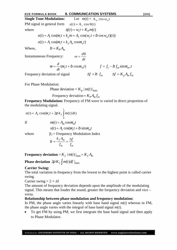
Single Tone Modulation: Let m(t) =PM signal in general form
where ( ) ( )c Pt w t K m t ( ) cos( cos( cos )( ))
( ) cos( cos )c c p C C m
c c p m m
x t A t k m A w t w t t
x t A t k A t
Where, P mK A
Instantaneous Frequency:
( cos )c md
t tdt
sin ,c m mf f f t
Frequency deviation of signal m p m mf f f K A f
For Phase Modulation:
p maxPhase deviation = K | ( ) |m t
Frequency deviation P m mK A fFrequency Modulation: Frequency of FM wave is varied in direct proportion ofthe modulating signal.
0
( ) cos( 2 ( ) )t
c c fx t A t k m t dt If ( ) cosm mm t A t
( ) cos( sinc c mx t A t t where f = Frequency Modulation Index
f m
m m
k A f
f f
Frequency deviation = max| ( ) |f f mK m t K A
Phase deviation max2 ( ) |fK m t df Carrier Swing:The total variation in frequency from the lowest to the highest point is called carrierswing.Carrier swing = 2 × fThe amount of frequency deviation depends upon the amplitude of the modulatingsignal. This means that louder the sound, greater the frequency deviation and vice –versa.Relationship between phase modulation and frequency modulation:In PM, the phase angle varies linearly with base band signal m(t) whereas in FM,the phase angle varies with the integral of base band signal m(t). To get FM by using PM, we first integrate the base band signal and then apply
to Phase Modulator.
A cosm mt( ) A cos ( )cx t t
d
dt

ECE FORMULA BOOK 8. COMMUNICATION SYSTEMS [236]
Published by: ENGINEERS INSTITUTE OF INDIA. ALL RIGHTS RESERVED www.engineersinstitute.com
PM wave may be generated by using frequency modulator by firstdifferentiating base band signal m(t) and then applying to the FrequencyModulator.
Power Carried by FM and PM signals: Since the Amplitude of Frequency andPhase modulated signal is constant, the power transmitted in FM and PM waves isindependent of modulation index
i.e.2
2c
tA
P
Because of constant Amplitude, Noise level in FM and PM can be kept withinlimits. That’s why it is used in Audio Communication.
Classification of FM signals:(1) Narrow Band FM signals (NBFM)(2) Wide Band FM signals (WBFM)
Narrow Band FM signal (NBFM): For these signals modulation index is less thanunity.
( ) sin2 mt f t [cos cos ( ) sin sin ( )]c c cA t t t t
is small, so cos ( ) 1,sin ( ) ( )}t t t ( ) cos sin sinc c c c mx t A t A t
cos cos cos2c
c c c m c mA
A t t t
Above signal is called NBFM signal. It has two bands similar to AM wave and bothhave same bandwidth requirements.The lower side band of NBFM is inverted version of upper side band of AM signal.It can be detected using Envelop Detector.
WBFM signal: ( ) )cos( )c n c mn
x t A J n t
A wideband FM signal has infinite number of side bands.Ideally the Bandwidth requirement of Fm signal is infinite because it has infinitenumber of side bands.Carson’s Law:Transmission Bandwidth of FM signal:BW = If (NBFM)
BW = If (WBFM) or 2( 1) mBW f 2( ) 2( 1)m mBW f or BW f
FM over AMIt is possible to reduce noise still further by increasing the frequency deviation butin AM this is not possible. Standard frequency allocations provide a guard band between commercial FM
stations. Due to this, there is less adjacent channel interference in FM.
( ) A cos[ ( )]c cx t t t { ( )t
2 mf 1
2( )mf f 1

ECE FORMULA BOOK 9. ELECTROMAGNETIC THEORY [265]
Published by: ENGINEERS INSTITUTE OF INDIA. ALL RIGHTS RESERVED www.engineersinstitute.com
9ELECTROMAGNETIC
THEORYCONTENTS
1. COORDINATE SYSTEMS AND VECTOR CALCULUS ….. 266-267
2. ELECTROSTATIC FIELDS …………………………………….. 268-271
3. MAGNETO STATIC FIELDS …………………………………… 272-274
4. MAXWELL’S EQUATIONS …………………………………….. 275-276
5. ELECTROMAGNETIC WAVES ……………………………….. 277-281
6. TRANSMISSION LINE ………………………………………….. 282-285
7. ANTENNAS ………………………………………………………… 286-286

ECE FORMULA BOOK 9. ELECTROMAGNETIC THEORY [266]
Published by: ENGINEERS INSTITUTE OF INDIA. ALL RIGHTS RESERVED www.engineersinstitute.com
1. COORDINATE SYSTEMS AND VECTORCALCULUS
Vector Calculus: Gradient: The gradient of scalar V is written as V and result is vector
quantity.
For Cartesian: x y z
V V Vˆ ˆ ˆV a a ax y z
For Cylindrical: ρ zV 1 V Vˆ ˆ ˆV a a a
z
For Spherical:r
V 1 V 1 Vˆ ˆ ˆV a a ar r r sin
Divergence: The divergence of vector A
is written as .A
and result is scalarquantity.
For Cartesian: yx zAA A
.Ax y z
For Cylindrical: zA A1 1
.A ( A )z
For Spherical: 2r2
A1 1 1.A (r A ) (sin A )
r r r sin rsin
Curl of vector: The curl of vector A
is defined as A
and result is vectorquantity.
For Cartesian:x y z
x y z
ˆ ˆ ˆa a a
Ax y z
A A A
For Cylinderical:
r z
z
a aa
Az
A A A
For Spherical:
r θ2
r
a a a
r sinθ r sinθ r
Ar
A rA rsin A

ECE FORMULA BOOK 9. ELECTROMAGNETIC THEORY [267]
Published by: ENGINEERS INSTITUTE OF INDIA. ALL RIGHTS RESERVED www.engineersinstitute.com
Laplacian of Scalar: Laplacian of scalar field V is written as V. It is thedivergence of gradient of V. The result is a scalar quantity.
For Cartesian:2 2 2
22 2 2
V V VV
x y z
For Cylinderical:2 2
22 2 2
1 V 1 V VV
z
For Spherical:2
2 22 2 2 2 2
1 V 1 V 1 VV r sin
r r r r sin r sin
Laplacian of Vector: It is a vector quantity.
2 A ( .A) A
Divergence of a curl of vector is always zero . ( A) 0
Curl of gradient of a scalar field is always zero ( V) 0
The vector field is said to be solenoidal or divergence less if . A 0
A vector field is said to be irrotational (or potential) if A 0
A vector field is said to be harmonic if 2 V 0
2A ( . A) A
. (A B) B . ( A) A . ( B)
Divergence Theorem: It states that total outward flux of vector field A
through
closed surface S is the same as volume integral of the divergence of A
.
s v
A.ds . A dv
Stokes’ Theorem: It states that line integral of a vector field A
over a closed path is
equal to surface integral of curl of A.
s
A . dl ( A) . dsl

ECE FORMULA BOOK 9. ELECTROMAGNETIC THEORY [268]
Published by: ENGINEERS INSTITUTE OF INDIA. ALL RIGHTS RESERVED www.engineersinstitute.com
2. ELECTROSTATIC FIELDS
Coulomb’s Law: Force between two point charges
12
1 212 2
Q Q ˆFR r
ka
Where, 919 10 m/ F
4 o
k
Electric Field Intensity: Force per unit charge when placed in electric field.
EE
Q
Electric Field Intensity due to Infinite long line charge:
L ˆE2 o
a
a Unit normal vector to line
Perpendicular distance of the point from line (minimum distance)
Electric Field Intensity due to Infinite charge sheet:
0
ˆE2
sna
s = surface charge density, ˆna unit vector Normal to sheetIn parallel plate capacitor, the electric field existing between the two plates having
equal and opposite charges;0
ˆE na

ECE FORMULA BOOK 9. ELECTROMAGNETIC THEORY [269]
Published by: ENGINEERS INSTITUTE OF INDIA. ALL RIGHTS RESERVED www.engineersinstitute.com
Electric Field Intensity due to uniformly charged sphere
0
3
02
ˆ ;03
E
ˆ ;3
o r
ro
ra r a
aa r a
r
o = volume charge density, a = radius of sphere
Electric Flux Density (
D ): 0D E
Electric Flux D .s
ds
Gauss’s Law: The total electric flux through any closed surface is equal to thetotal charge enclosed by surface.
VQ D.s v
ds dV
V. D
Electric Potential:B
AB
A
W 1 1V E .dl
Q 4 B Ao B A
QV V
r r
Negative sign indicates that the work is being done by external agent.
ABV = potential difference between A and BPotential at any point r due to point charge Q located at origin is
0
QV
4 r
Potential between two points in the field of point charge AB0
Q 1 1V
4 b ar r
Work done while moving a charge in electric field is independent of path followed.It depends only on initial and final paths.
W Q E . dl 0
E 0
Electro static field is conservative or irrotational.
Energy density of Electro static field
WE =1
D . E2
22
E
1 1 DW E
2 2
The gradient of potential field gives the electric field intensity. The electric fieldintensity in terms of potential is given by
E V

ECE FORMULA BOOK 9. ELECTROMAGNETIC THEORY [270]
Published by: ENGINEERS INSTITUTE OF INDIA. ALL RIGHTS RESERVED www.engineersinstitute.com
Electric flux line is an imaginary path or line drawn in such a way that itsdirection at any point is the direction of the electric field at that point connection
current density J v u
v Charge density u
charge velocity
Conduction current density J E
where2ne
m
A perfect conductor cannot contain an electrostatic field within it.
Inside a conductor E
= 0, 0,v V 0ab
Dielectric constant and polarization:
0 0D (1 ) E Ee r
0D E P
where 0P Ee e
0
1r e
e Electric susceptibility
Dielectric strength is maximum electric field that a dielectric can tolerate towithstand breakdown.
Continuity Equation . J v
t
Relaxation Time Tr
/ rt Tv vo e
Boundary Conditions:Dielectric – Dielectric Boundary Conditions:Tangential Component Relation
1 2E Et t or 1 2
1 2
D Dt t
Normal Component Relation: 1 2D Dn n s
s Free charge density placed at boundary.
The tangential component Et is continuous across the boundary and tangentialcomponent D t is discontinuous at boundary.
The normal component of D
is continuous while that of E
is discontinuous atboundary.
1 1
2 2
tan
tanr
r
This is the law of refraction of the electric field at a boundary free of charge.Conductor – Dielectric Boundary:
D E 0, D Et o r t n o r n s

ECE FORMULA BOOK 10. MEASUREMENTS & INSTRUMENTATION [287]
Published by: ENGINEERS INSTITUTE OF INDIA. ALL RIGHTS RESERVED www.engineersinstitute.com
10MEASUREMENTS
&INSTRUMENTATION
CONTENTS
1. MEASURING INSTRUMENT CHARACTERISTICS ……. 288-289
2. CLASSIFICATION OF ELECTRICAL INSTRUMENTS… 290-295
3. AC BRIDGES ……………………………………………………… 296-298
4. MEASUREMENT OF POWER & WATTMETERS ……….. 299-301
5. MEASUREMENT OF RESISTANCE ……………………….. 302-302
6. Q-METER ………………………………………………………….. 303-303
7. TRANSDUCERS ………………………………………………… 304-306
8. CRO (CATHODE RAY OSCILLOSCOPE) ………………… 307-308

ECE FORMULA BOOK 10. MEASUREMENTS & INSTRUMENTATION [288]
Published by: ENGINEERS INSTITUTE OF INDIA. ALL RIGHTS RESERVED www.engineersinstitute.com
1. MEASURING INSTRUMENTCHARACTERISTICS
Generalized Measuring Instrument: The block diagram of generalized measuringsystem may be represented as:
IMPORTANT DEFINITIONS:Accuracy: Closeness with which an instrument reading approaches the true valueof the variable being measured. It can be improved by recalibration.Precision: It is a measure of the degree to which successive measurement differfrom one another. It is design time characteristic.High precision does not mean high accuracy. A highly precise instrument may beinaccurate.Ex: If reading are 101, 102, 103, 104, 105. Most precise value is 103Resolution: The smallest change in measured value to which the instrument willrespond. It is improved by re-calibrating the instrument.Sensitivity: It is ratio of change in output per unit change in input quantity of theinstrument. It is design time characteristic.Drift: It means deviation in output of the instrument from a derived value for aparticular input.Reproducibility: It is degree of closeness with which a given value may bemeasured repeatedly for a given period of time.Repeatability: It is degree of closeness with which a given input is repeatablyindicated for a given set of recordings.Errors:1. Absolute Error/Static Error/Limiting Error:
TA A Am Am Measured value of quantity of actual value
TA True value of quantity or nominal value
2. Relative Error: T
T T
A AA
A Am
r
3. Percent Error:T
A% 100
Ar
Instrument Error is generally given in percent error.
4. Percentage Error at reading ‘x’:
,
Full Scale Reading% [% , Full scale]r x rx

ECE FORMULA BOOK 10. MEASUREMENTS & INSTRUMENTATION [289]
Published by: ENGINEERS INSTITUTE OF INDIA. ALL RIGHTS RESERVED www.engineersinstitute.com
Error due to combination of quantities:1. Error due to Sum/Difference of quantities
1 2X x x
1 1 2 2
1 2
X%
X X Xr
x x x x
x x
2. Error due to product or quotient of quantities
1 2 3X x x x Or 1
2 3
x
x xor
1 2 3
1
x x x
31 2
1 2 3
X
X
xx x
x x x
3. Composite factors 1 21 2
1 2
XX x .
Xn m x x
x n mx x
CLASSIFICATION OF ERRORS:
Standards of EMF:(a) Saturated Weston cell is used for Primary standard of emf.
Its emf is 1.01864 volt, maximum current drawn is 100 A. It contains
4CdSO crystal and its internal resistance is 600 to 800 . (b) Unsaturated Weston cell is used for secondary standards. Its emf is 1.0180
to 1.0194 volt and does not have 4CdSO crystal.Standard of Resistance:Maganin (Ni + Cu + Mn)
Nickel 4%
Magnese12% [High Resistivity and low temperature coefficient]
Copper 84%
Inductive effect of resistance can be eliminated, using Bifilar winding.Standard of Time and Frequency:Atomic clock is used as primary standard of time and frequency. Quartz, Rubidiumcrystal is used as secondary standard of time and frequency. Example: Cesium 133,hydrogen maser etc.

ECE FORMULA BOOK 10. MEASUREMENTS & INSTRUMENTATION [290]
Published by: ENGINEERS INSTITUTE OF INDIA. ALL RIGHTS RESERVED www.engineersinstitute.com
2. CLASSIFICATION OF ELECTRICALINSTRUMENTS
Absolute Instrument: It gives the value of parameters under measurement in termsof the physical constant of the instrument.e.g. Transient Galvanometer, Rayleigh current balance etc.
Secondary Instrument:It gives the value of parameter for directly under measurement.e.g. voltmeter, thermometer, pressure gauge etc.Note: Absolute instruments are highly accurate than secondary instrument as theycontain less number of moving mechanical parts resulting in a lower operational ofpower consumption.
Classification of analog instruments1. Indicating type: Voltmeter, Ammeter, Wattmeter .2. Recording type: Recorders.3. Integrating type: Energy meter.4. Comparison type: Potentiometer and bridges or null deflection.5. Deflecting type: PMMCNote: Null deflecting instruments are highly accurate as compression to deflectinginstrument as their operational power consumption at zero deflection is zero.
Principle of Operation of Analog Instruments:Magnetic effect: Moving Iron, PMMC, DynamometerInduction effect: Energy meterHeating effect: Thermocouple and Hotwire type, BolometerElectro static effect: Electro static type voltmeterHall Effect: Poynting vector type voltmeter, Flux-meterDamping system used in indicating instruments:It is provided in the instrument which helps the moving system of the instrument toreach to final position at earliest.

ECE FORMULA BOOK 10. MEASUREMENTS & INSTRUMENTATION [291]
Published by: ENGINEERS INSTITUTE OF INDIA. ALL RIGHTS RESERVED www.engineersinstitute.com
Electromagnetic damping: Galvanometer and moving coil typeEddy current damping: PMMC voltmeter and energy meterAir frictional damping: Moving iron and dynamometerFluid friction damping: Electrostatic type voltmeter PMMC Instruments are used only for DC measurements. Induction type instruments are used only for AC measurements. Hotwire and Thermal type instruments measure RMS value of input. Electrostatic type instruments are used to measure high voltages in kV. Rectifier type instruments responds to average value.
Permanent Magnet Moving Coil instruments: These are also called self shielding instruments. Aluminium former is used to provide eddy current damping.
Magnetic field in these is in range of 0.1 to21wb/ m which is strong field.
Control spring which is made of phosphor-bronze material in these instrumentsprovides a control force and also provides a path for current entering to movingcoil.
If control spring is broken, current through the coil is zero and instrument readszero.
It is used for measurement of DC only. Material used for magnet in PMMC is Alnico and Alcomax (Al + Co +Ni). Torque to weight ratio of the moving system should be high and equal to 0.1,
0.1 ; It decides sensitivity which is high in PMMCT
weight
It can sense a current upto 50 A. Deflecting torque (Td) = NBAI Controlling torque (Tc) = k
At balance Td = Tc
G NBAI I
K K
N Number of turns A Area of cross section of vowing coilB Magnetic flux I Current through coilKey points:The control spring in PMMC have dual utility, they not only produce controllingtorque but also used to lead the current into the system.
Source of Errors: Ageing effect of the permanent magnet (can be reduced by using a pre-edged
magnet) Temperature effect of coil and the control spring.

ECE FORMULA BOOK 11. MATERIALS SCIENCE [309]
Published by: ENGINEERS INSTITUTE OF INDIA. ALL RIGHTS RESERVED www.engineersinstitute.com
11MATERIALS SCIENCE
CONTENTS
1. STRUCTURE OF MATERIALS …………………………… 310-311
2. ELECTRIC MATERIALS & PROPERTIES ……………. 312-315
3. CONDUCTIVE MATERIALS ……………………………… 316-318
4. MAGNETIC MATERIALS …………………………………. 319-322

ECE FORMULA BOOK 11. MATERIALS SCIENCE [310]
Published by: ENGINEERS INSTITUTE OF INDIA. ALL RIGHTS RESERVED www.engineersinstitute.com
1. STRUCTURE OF MATERIALS
1. Simple Cubic (SC): Distance between adjacent atoms SC 2d a r Coordination number = 6
No of atoms per unit cell =1
8 corners part 18
Packing efficiency = 52%Example Polonium, Fluorspar
2. Body Centered Cubic (BCC):
Distance between adjacent atom BCC
32
2d r a
Coordination number = 8
No of atoms per unit cell =1
8 1 28
Packing efficiency = 68%
Example Fe, Cr, Na
3. Face Centered Cubic (FCC):
Distance between adjacent atoms FCC 22
ad r
Coordination number = 12
No of atoms per unit cell =1
8 3 48
Packing efficiency = 74%Example Cu, Silver, Gold
Hexagonal Closed Pack (HCP): Coordination number = 12
No of atoms per unit cell =1
12 3 412
Packing efficiency = 74%Example Cd, Mg
Different types of unit cell
Type of unit cell Volume of unit cellCubic a3
Tetragonal a2cOrthorhombic a b c
Hexagonal23 3a c
2

ECE FORMULA BOOK 11. MATERIALS SCIENCE [311]
Published by: ENGINEERS INSTITUTE OF INDIA. ALL RIGHTS RESERVED www.engineersinstitute.com
Crystallographic Plane and Miller Indices:Miller indices are used to specify directionsand planes and it could be in lattices or incrystals.Miller Indices for plane A B C
OA OB OC, ,
OA OB OCh k
Example:1.
OA2
OA2
h
OB0k
OC
0
( , , ) (2, 0, 0)h k
2.OA
1OA
h
OB1
OBk
OC1
OC
( , , ) (1,1,1)h k
3.
1
0
0
( , , ) (1, 0, 0)
OAh
OAOB
k
OCl
h k l

ECE FORMULA BOOK 11. MATERIALS SCIENCE [312]
Published by: ENGINEERS INSTITUTE OF INDIA. ALL RIGHTS RESERVED www.engineersinstitute.com
2. ELECTRIC MATERIALS & PROPERTIESDielectric Constant:
D
E D: Electric flux density, E: Electric field Intensity
o r : permittivity of the medium (farad per meter)
910F/ m :Relative permittivity
36o r
Dipole Moment: Product of either of two charges and separation between charges.
p q r
Coulomb-meter
Polarization:
It is defined as electric dipole moment per unit volume. It is denoted by P
.
2P N coulomb/mp
N Number of dipoles per unit volume
Polarizability: P E
Polarizability, 2F m
E
Electrical Field Intensity, V/m,
p
Dipole moment, coulomb-mElectric flux density: When an electric field is applied
D E P E Eo o o e
Polarization P E ( 1) Eo e o r
1e r
Polarization:(a) Electronic/Induced Polarization: It is found in materials like inert gases in
which there is no reaction among individual molecules.
P N Ee e
Electronic polarizabilitye
(b) Ionic Polarization: It is found in materials possessing ionic bonds betweentwo dissimilar atoms like NaCl, HCl.These materials have permanent dipole moment in absence of external fieldand exhibits both electronic and ionic polarization.
P P P N( )Ei e i e
i Ionic polarizability(c) Orientational Polarization: Occurs in materials having partly ionic bonds like
2 2H O, CO .

ECE FORMULA BOOK 11. MATERIALS SCIENCE [313]
Published by: ENGINEERS INSTITUTE OF INDIA. ALL RIGHTS RESERVED www.engineersinstitute.com
2pNp E
P N E3kT o
where orientation polarization2
pp
3kTo
k Boltzman1P
T TemperatureT
(d) Interfacial polarization: It is the result of lattice vacancies in the dielectrics.Total polarization TP P P P Pi e o s Ps Interfacial polarization
When alternating fields is applied, relative dielectric constant become functionof frequency and at frequency about visible/optical ranges 51014Hz materialpossesses only electronic polarization.
Langevin-Debyes generalization of the Clausius-mossotti equation
N 1
3 2e r
o r
N Number of molecules per unit volume e Electronic PolarizabilityIt is applicable for gaseous states only.
Lorentz Equation:2
2
N 1 M
3 2 Po
n
n
It is applicable only for electronic polarization i e at optical frequencies.Piezoelectric Materials: If mechanical stress is applied to a dielectric material,material gets polarized because of applied stress and vice versa. These types ofmaterials are called piezoelectric materials.
Example: Quartz crystal, Rochelle salt, Barium Titanate 3(Ba TiO ), Lead Zirconate
3(PbZr O ).
Applications: Gramophone, Accelerometer. Some dielectric materials get strained when they are subjected to an electric field
but reverse effect is not found. Then this property is Electrostriction.
Expression of voltage sensitivity:F Q
V gt P tA Co r
e
g = voltage sensitivity =o r
d
volt-meter/Newton; t Thickness
P =F
Astress applied; A Area of cross section of crystal

ECE FORMULA BOOK 12. COMPUTER ORGANIZATION [323]
Published by: ENGINEERS INSTITUTE OF INDIA. ALL RIGHTS RESERVED www.engineersinstitute.com
12COMPUTER ORGANIZATION
CONTENTS
1. PROGRAMMING BASICS ………………………………………. 324-328
2. MEMORY ACCESS AND DMA ………………………………… 329-334
3. DATA STRUCTURES ……………………………………………. 335-336

ECE FORMULA BOOK 12. COMPUTER ORGANIZATION [324]
Published by: ENGINEERS INSTITUTE OF INDIA. ALL RIGHTS RESERVED www.engineersinstitute.com
1. PROGRAMMING BASICSComputer cannot execute a program written in assembly or high level language.The program first must need to be translated to machine language (machinelanguage program is nothing more than sequence of 0s and 1s) which the computercan understand.
Compiler: Compiler is a translator, which converts high level language programinto assembly language program.Assembler: Assembler is a program that translates assembly language program intomachine language (sequence of 0s and 1s) program.Linker: Linker is a computer program that takes one or more object files generatedby a compiler and combine them into a single executable program.Loader: Loader is the part of an operating system that is responsible for loadingprograms. It places programs into memory and prepares them for execution.
Data types in C:Data type Size (in bytes)char 1int 2float 4double 8
int i = 10;This declaration tells the C compiler to:
(a) Reserve space (2B) in memory to hold the integer value.(b) Associate the name i with this memory location.(c) Store that value of i at this location
10
1000
i Location name
Value at location
Address
main ( ){
int i = 10;printf (“%u”, &i);printf (“%d”, i);printf (“%d”, * (&i));
}Output:/*printf (“%u”, &i); */ 1000/*printf(“%d”, i); */ 10/*printf(“%d”, * (&i)); *(1000) = 10* is called “value at address” operator.Pointer: Pointers are variables which holds the address of another variable.

ECE FORMULA BOOK 12. COMPUTER ORGANIZATION [325]
Published by: ENGINEERS INSTITUTE OF INDIA. ALL RIGHTS RESERVED www.engineersinstitute.com
Example:main( )
{
int x = 5;
int * y = &x;
int**z = &y;
prin tf("%u",&x);
prin tf("%u",y);
prin tf("%u",z);
printf("%d",x);
printf("%d",*y);
printf("%d",**z);
}
Solution:5
1000 1001
1000
2000 2001
2000
3000 3001
x
y
z
printf("%u",&x); 1000
printf("%u",y); 1000
printf("%u",z); 2000printf("%d",x); 5
printf("%d",*y); *1000=5
printf("%d",**z); **2000=*1000=5Note: Every pointer variable takes 2 byte

ECE FORMULA BOOK 12. COMPUTER ORGANIZATION [326]
Published by: ENGINEERS INSTITUTE OF INDIA. ALL RIGHTS RESERVED www.engineersinstitute.com
Parameter Passing Techniques:1. Call by value2. Call by reference
Call by value:Actual values of the parameter are passed to the called function.
Example: What is the output of the following program using Call by value asparameter passing technique?
main( ) swap(int c, int d)
{ {
int a=10; int t;
int b=20; t=c;
printf ("%d%d",a,b); c=d;
swap(a,b); d=t;
printf ("%d%d",a,b); }
}
Solution:Execution of program always starts from main ( )
Here, the changes will not reflect because we are passing the value of parameter tothe function.
Call by reference:In Call by reference, addresses of variables are passed as parameter to the calledfunction.
Example: What is the output of above program, if compiler uses call by referenceas parameter passing technique?Solution: If compiler uses call by reference parameter passing technique, followingchanges are made to the program by the compiler.

ECE FORMULA BOOK 13. MICROWAVES [337]
Published by: ENGINEERS INSTITUTE OF INDIA. ALL RIGHTS RESERVED www.engineersinstitute.com
13MICROWAVES
CONTENTS
1. MICROWAVE BASICS AND TRANSMISSION LINES …. 338-340
2. WAVEGUIDES ……………………………………………………. 341-344
3. MICROWAVE HYBRID CIRCUITS …………………………. 345-347
4. MICROWAVE MEASUREMENT DEVICES ………………. 348-348
5. MICROWAVE TUBES AND CIRCUITS ………………….. 349-353
6. MICROWAVE SEMICONDUCTOR DEVICES …………… 354-360
7. MICROWAVE COMMUNICATIONS ………………………. 361-364

ECE FORMULA BOOK 13. MICROWAVES [338]
Published by: ENGINEERS INSTITUTE OF INDIA. ALL RIGHTS RESERVED www.engineersinstitute.com
1. MICROWAVE BASICS AND TRANSMISSIONLINES
Microwaves are electromagnetic waves of which frequency ranges from 1 GHzto 1000 GHz.
Microwaves behave more like rays of light than ordinary radio waves.
Microwave frequency cannot be used for ground wave communication.
Advantages of Microwaves:1. Increased bandwidth availability 2. Improved directive properties3. Low fading effect and low power requirements
IEEE bands For microwaveL 1.1 – 1.7 GHzLs 1.7 – 2.6 GHzS 2.6 – 3.9 GHzC 3.9 – 8 GHzX 8 – 12.5 GHzKu 12.5 – 18 GHzK 18 – 26 GHzKa 26 – 40 GHz
Propagation characteristics and applications of various bands:Band Frequency Wavelength Propagation
characteristicsApplications
ELF 30 – 300 Hz 10 – 1 Mm Penetration into earthand sea.
Communication withsubmarines.
VLF 3 – 30 kHz 100 –10 km Surface wave up to1000 km. Sky wave in
the night extendsrange. Low attenuationduring day and night.
Long distance point topoint communication,
Sonar navigation.
LF 30 – 300 kHz 10 – 1 km Surface wave and skywave at night. Surface
wave attenuationgreater than VHF.
Point-to-point marinecommunication, Time
standard frequencybroadcast.
MF 300–3000 kHz 1000–100m Ground wave in dayand sky wave in night.Attenuation is high inday and low in night.
AM broadcasting,direction finding,
coastguard and marinecommunication.
HF 3 – 30 MHz 100 – 10 m Reflection fromionosphere.
Moderate and longdistance communicationof all types: telephone,
telegraph, radio.VHF 30 – 300 MHz 10 – 1 m Space wave, line of
sight.Television FM service,
aviation and police.UHF 300–3000 MHz 100 –10 cm Same as VHF, affected
by tall objects likehills.
Short distancecommunication,
including radar, T.V,satellite communication.

ECE FORMULA BOOK 13. MICROWAVES [339]
Published by: ENGINEERS INSTITUTE OF INDIA. ALL RIGHTS RESERVED www.engineersinstitute.com
Microwave Transmission LinesMulti-conductor lines:Coaxial cable: It is used upto 3GHz and it behaves like a LPF. Coaxial cables support TEM wave and has no cut off frequency. There is high radiation loss in coaxial cable at high frequencies.
Coaxial cable resistance:1 1 1
/2 c
R ma b
Skin depth Conductivity
a Inner conductor radius b Outer conductor radius
Inductance: L =μ b
ln H/m2π a
Capacitance:2
C F/mb
lna
Characteristic Impedance: L 1Z
C 2o
bn
a
60Z lno
r
b
a
Breakdown power in coaxial cable: 23600bd
bP a ln KW
a
Strip Lines: These are modifications of coaxial lines and used at frequency from 100 MHz to
100 GHz. The dominant mode is TEM mode and has no radiation losses. These have higher isolation between adjacent circuits and no fringing fields after
a certain distance from the edges of a conductor. It is difficult to mount active components on strip lines (i.e. line diode,
circulators).
Characteristic Impedance:60 4
or
bZ ln
d
d Diameter of circular conductorb Thickness between ground plates
c
ECE FORMULA BOOK 13. MICROWAVES [340]
Published by: ENGINEERS INSTITUTE OF INDIA. ALL RIGHTS RESERVED www.engineersinstitute.com
Micro strip lines: Cost is lower than strip line, coaxial cable or waveguide. Open structure of microstrip line leads to greater coupling and it is large to
mount passive or active components. Open structure also leads to higher radiation losses and interference due to
nearby conductors. Due to this interference a discontinuity in electric and magnetic field presents
and this leads to impure TEM or quasi TEM modes.Characteristic Impedance:
60 4Zo
r
hn
d
If h >> d
377Zo
r
h
w
If w >> h
w strip line width t thicknessh distance between the line and ground plane.
ECE FORMULA BOOK 13. MICROWAVES [341]
Published by: ENGINEERS INSTITUTE OF INDIA. ALL RIGHTS RESERVED www.engineersinstitute.com
2. WAVEGUIDESWaveguides (single conductor lines) At frequencies higher than 3 GHz, there are more losses in Transmission lines. A hollow metallic tube used to transmit EM waves by successive reflections
from inner walls of tube is called waveguide.
Difference with transmission line: In waveguides, only waves having frequencies greater than cut off frequency cf
will be propagated that is why waveguide act as a HPF. Waveguide is one conductor transmission line.
Rectangular waveguide: 11TM is dominant mode for TM waves.
TE10 is dominant mode for TE wave and it is also overall dominant mode(when a > b).
In this 10TM or 01TM does not exist.
Cut off frequency:2 2
1
2c
m nf
a b
Phase constant :
2
1 cf
f
Phase velocity:2
1
1
p
c
vf
f
Group velocity:
21
1 cg
fv
f
In waveguide: p gv c v
i.e. 2p gv v c
In vacuum: p gv c v