handbuch canopen standard pio-337 mit ... - parker hannifin · electromechanical automation north...
TRANSCRIPT
Electromechanical Automation North America
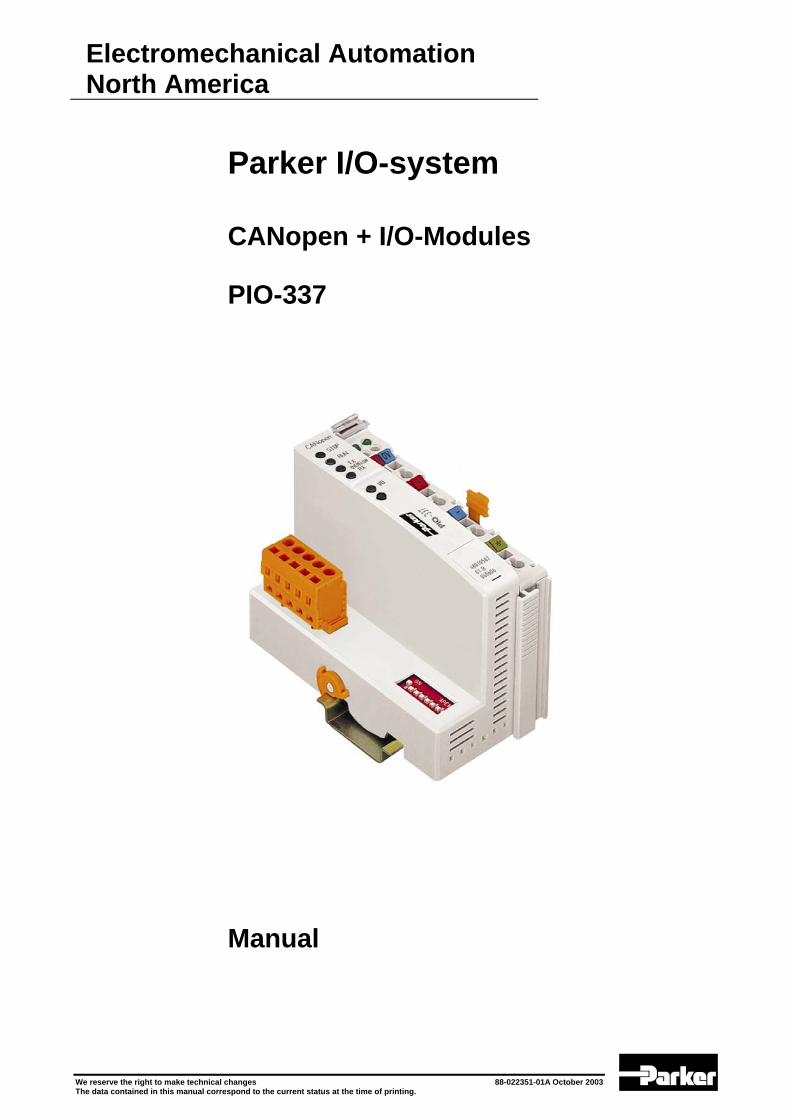
Parker I/O-system
CANopen + I/O-Modules
PIO-337
Manual
We reserve the right to make technical changes 88-022351-01A October 2003 The data contained in this manual correspond to the current status at the time of printing.

PIO Parker I/O-System
Technical description, installation and configuration
88-022351-01A October 2003 ii

88-022351-01A October 2003 iii

PIO Parker I/O-System
TABLE OF CONTENTS 1 Important comments ............................................................................................ 5 1.1 Legal principles ................................................................................................ 5 1.2 Symbols ........................................................................................................... 6 1.3 Font Conventions............................................................................................. 7 1.4 Number Notation.............................................................................................. 7 1.5 Safety Notes..................................................................................................... 8 1.6 Scope ............................................................................................................... 9 1.7 Abbreviation ..................................................................................................... 9
2 I/O-SYSTEM......................................................................................................... 10 2.1 I/O-system Description................................................................................... 10 2.2 Technical Data ............................................................................................... 11 2.3 Manufacturing Number .................................................................................. 15 2.4 Storage, Assembly and Transport ................................................................. 16 2.5 Mechanical Setup .......................................................................................... 16 2.6 Power Supply................................................................................................. 24 2.7 Grounding ...................................................................................................... 28 2.8 Shielding (Screening)..................................................................................... 31 2.9 Assembly Guidelines / Standards.................................................................. 31
3 Fieldbus coupler................................................................................................. 32 3.1 Fieldbus coupler............................................................................................. 32
4 I/O Modules ......................................................................................................... 59 4.1 PIO-400 [2 DI DC 24 V 3.0 ms, high-side switching]..................................... 59 4.2 PIO-402 [4 DI DC 24 V 3.0 ms, high-side switching]..................................... 62 4.3 PIO-430 [8 DI DC 24 V 3.0 ms, high-side switching]..................................... 65 4.4 PIO-468 [4 AI DC 0-10 V, Single-Ended]....................................................... 68 4.5 PIO-480 [2 AI 0-20 mA Differential Measurement Input] ............................... 72 4.6 PIO-501 [2 DO DC 24 V 0.5 A, high-side switching] ..................................... 76 4.7 PIO-504 [4 DO DC 24 V 0.5 A, high-side switching] ..................................... 79 4.8 PIO-530 [8 DO DC 24 V 0.5 A, high-side switching] ..................................... 82 4.9 PIO-550 [2 AO DC 0-10 V]............................................................................. 85 4.10 PIO-552 [2 AO 0-20 mA]................................................................................ 89 4.11 PIO-600 [End Module] ................................................................................... 93 4.12 PIO-602 [24 V DC Power Supply].................................................................. 95
5 CANopen ............................................................................................................. 98 5.1 Description ..................................................................................................... 98 5.2 Network architecture ...................................................................................... 99 5.3 Network communication .............................................................................. 104
6 Use in Hazardous Environments .................................................................... 157 6.1 Foreword...................................................................................................... 157 6.2 Protective measures .................................................................................... 157 6.3 Classification meeting CENELEC and IEC.................................................. 157 6.4 Classifications meeting the NEC 500 .......................................................... 161 6.5 Identification................................................................................................. 163 6.6 Installation regulations ................................................................................. 165
7 Glossary ............................................................................................................ 166
8 Literature list..................................................................................................... 167
9 Index .................................................................................................................. 168
88-022351-01A October 2003 4

EMN
88-022351-01A October 2003 5

PIO Parker I/O-System
1 Important comments fast installation and start-up of the units described in this manual, we
n is carefully read and adhered to.
1.1 Legal pr
righ
electronic and photo-technical ng and amendments require the written consent. Non-observance will entail
.1.2 P rsonn n
he use of the product detailed in this manual is exclusively geared to specialists trical specialists or persons instructed
by electrical specialists who are also familiar with the valid standards. The manufac-turer declines all liability resulting from improper action and damage to products and third party products due to non-observance of the information contained in this man-ual.
1.1.3 Intended use
For each individual application, the components supplied are to work with a dedi-cated hardware and software configuration. Modifications are only admitted within the framework of the possibilities documented in the manuals. All other changes to the hardware and/or software and the non-conforming use of the components entail the exclusion of liability.
To ensurestrongly recommend that the following information and explanatio
inciples
1.1.1 Copy t
This manual is copyrighted, together with all figures and illustrations contained therein. Any use of this manual which infringes the copyright provisions stipulated herein, is not permitted. Reproduction, translation and archivithe right of claims for damages.
1 e el qualificatio
Thaving qualifications in PLC programming, elec
88-022351-01A October 2003 6

EMN
1.2 Symbols
Danger Always abide by this rsons from injury. information to protect pe
Warning ays abide by thisAlw information to prevent damage to the device.
Attention M rg nal conditions ma i ust always be observed to ensure smooth operation.
ESD (Electrostatic Ding of damage bserve the pre-
cautionary measure for handling components at risk.
ischarge) Warn to the components by electrostatic discharge. O
Note Routines or advice for efficient use of the device and software optimization.
i
More information References on additional literature, manuals, data sheets and INTERNET pages
88-022351-01A October 2003 7

PIO Parker I/O-System
1.3 Font Conventions Names of path and files are marked italic
a sequence of menu
marked as bold with small capitals i.e.: ENTER
r. END_VAR
1.4 Number
Italic i.e.: C:\programs\
Italic Menu items are marked as bold italic i.e.: Save
\ A backslash between two names marks items i.e.: File\New
END Press buttons are
< > Keys are marked bold within angle brackets i.e.: <F5>
Courier Program code is printed with the font Couriei.e.:
Notation
Number Code Example Note
Decimal 100 normal notation
Hexadecimal 0x64 C notation
Binary '100' '0110.0100'
Within ', Nibble separated with dots
88-022351-01A October 2003 8

EMN
1.5 Safety Notes
Attention Switch off the I/O-system prior to working on bus modules! In the event of deformed contacts, the module in question is to be replaced, as its
ensured on a long-term basis.
having seeping and insulating als is: e.g. aerosols, silicones, triglyc-
erides (found in some hand creams).
t be ruled out that these materials appear in the component environment, then additional measures are to be taken:
dling of the com
functionality can no longer be
The components are not resistant against materials properties. Belonging to this group of materi
If it canno
- installation of the components into an appropriate enclosure - han ponents only with clean tools and materials.
Attention with ethyl alcohol and leather cloths.
use any conta mpair the functioning of the contact
ical operation rooms. Access must only be given via a key or tool to authorized qualified personnel.
and guidelines concerning the installa-
Cleaning of soiled contacts may only be done Thereby, the ESD information is to be regarded.
Do not ct spray. The spray may iarea.
The I/O-SYSTEM and its components are an open I/O-system. It must only be as-sembled in housings, cabinets or in electr
The relevant valid and applicable standards tion of switch boxes are to be observed.
ESD (Electrostatic Dic components that may be destroyed by he modules, ensure that the environment ll grounded. Avoid touching conductive com-
s, e.g. gold co
scharge) The modules are equipped with electronielectrostatic discharge. When handling t(persons, workplace and packing) is weponent ntacts.
88-022351-01A October 2003 9

PIO Parker I/O-System
1.6 Scope This document is an extractThis manual describes the m
from the CANopen manual. odular I/O-SYSTEM with the fieldbus coupler for
CANopen.
Components
Fieldbus coupler CANopen, 10 kBaud – 1 MBaud
1.7 AbbreviAnalog Input
etwork
EMCY Emergency Object
Idx Index
M Master
NMT Network Management
PDO Process Data Object
RO Read Only
RTR Remote Transmit Request
RxPDO Receive PDO
RW Read/Write
SDO Service Data Object
S-Idx Sub-Index
TxPDO Transmit PDO
ation
AI
AO Analog Output
BC Buscoupler
CAL CAN Application Layer
CAN Controller Area N
COB ID Communication Object Identifier
DI Digital Input
DO Digital Output
I/O Input/Output
ID Identifier, Identification
88-022351-01A October 2003 10
EMN
2 I/O-SYSTEM 2.1 I/O-syste ription
The I/O-SYSTEM is a modular, fieldbus independent I/O-system. It is comprised of a fieldbus coupler (1) and up to 64 connected fieldbus modules (2) for any type of sig-nal. Together, these make up the fieldbus node. The end module (3) completes the n
m Desc
ode.
PIO-400
+ +
E1 E2
DE DE
PIO-400
+ +
E3 E4
DE DE
+ +
PIO-XXX
E5 E6
AE AE
PIO-501
+ +
A1 A2
DA DA
PIO-501
+ +
A3 A4
DA DA
PIO-501
+ +
A5 A6
DA DA
PIO-501
+ +
PIO-XXX
+ +
A7 A8
DA DA
A9 A10
AA AA
PIO-602
+ +
PIO-602
+ +
PIO-602
+ + + +
PIO-XXX
E8E7
AE AE
+ +
PIO-XXX
A11 A12
AA AA
+ +
PIO-XXX
E9 E10
AE AE
PIO-602
+ +
PIO-501
+ +
A13 A14
DA DA
PIO-600
CANERR
TxOverflowRx
I/O RUN
I/O ERR
1 3
Fig. 2-1: Fieldbus node
C stems su Nopen, DeviceNet are a
T s int , electronics and a power supply terminal. T ce forms the phy relevant fieldbus. The elec-t ta of the bus m t available for the fieldbus communication. The 24 V I/O-system supply and the 24 V field supply are fed in via th ower supply terminaThe fieldbus coupler communicates via the relevant fieldbus.
B igital and tions as well as special functions can be connected to the coupler. The communication between the coupler and the b out via an int
The I/O-SYSTEM has a clear port level with LEDs ertable m ut group -mented by a ground wire connection allows for direct sensor/actuator wiring.
2
RUN
ouplers for fieldbus I/O-syvailable.
ch as PROFIBUS, CA
he coupler contains the fieldbu erfacehe fieldbus interfa
ronics process the dasical interface to theodules and make i
e integrated p l.
us modules for diverse d analog I/O func
us modules is carried ernal bus.
for status indication, insini WSB markers and pullo marker carriers. The 3-wire technology supple
88-022351-01A October 2003 11

PIO Parker I/O-System
2.2 Technical Data
Mechanic
Material Polycarbonate, Polyamide 6.6
Dimensions - Coupler - I/O module, single - I/O module, double
x 64* mm x 100 mm
- 51 mm x 65* mm x 100 mm - 12 mm- 24 mm x 64* mm x 100 mm * from upper edge of DIN 35 rail
Installation on DIN 35 with interlock
modular by featherkey-dovetail double
Mounting position any position
Length of entire node ≤ 831 mm
Marking marking label type 247 and 248 paper marking label 8 x 47 mm
Wire range
Wire range
CAGE CLAMP® Connection 0,08 mm² ... 2.5 mm² AWG 28-14 8 – 9 mm Stripped length
Contacts
Power jumpers contacts blade/spring contact self-cleaning
Current via power contactsmax 10 A
Voltage drop at Imax < 1 V/64 modules
Data contacts slide contact, hard gold plated 1,5µm, self-cleaning
Climatic environmental conditions
Operating temperature 0 °C ... 55 °C
Storage temperature -20 °C ... +85 °C
Relative humidity 95 % without c ensation 5% to ond
Resistance to harmful s acc. To IEC 60068-2-42 and IEC 60068-2-43 ub-stances
Maximum pollutant concentration at relative humidity < 75%
SOH
2 25 ppm 2S ≤ 10 ppm
≤
Special conditions Ensure that additional measures for compo-nents are taken, wh used in an e iron-
ent involving:
ionization ra
ich are nvm– dust, caustic vapors or gasses – diation.
88-022351-01A October 2003 12

EMN
Mechanical strength
Vibration resistance 0068ent to the v of oscillap with a ra ave per
0 Hz ≤ f < 57 Hz, const. Amplitude 0,075 mm 57 Hz ≤ f < 150 Hz, const. Acceleration 1 g b) Period of oscillation:
acc. to IEC 6 -2-6 Comm ibration restistance: a) Type swee
tion: te of change of 1 oct
minute 1
10 sweep per axis in each of the 3 vertical axes
Sh
ulse: half sinusoidal
Route of impulse: 3 impulses in each pos. And neg. direction of the
f the test object, this means
ock resistance acc. to IEC 60068-2-27 Comment to the shock restistance: a) Type of impb) Intensity of impulse: 15 g peak value, 11 ms maintenance time c)
3 vertical axes o 18 impulses in all
Free fall -2-32 acc. to IEC 60068≤ 1m (module in original packing)
Safe electrical isolation
Air and creepage distance acc. to IEC 60664-1
Degree of protection
Degree of protection IP 20
Electromagnetic compatibility*
Directive Test values Strength class
Evaluation criteria
Immunity to interference acc. to EN 50082-2 (96)
EN 61000-4-2 4kV/8kV (2/4) B
EN 61000-4-3 10V/m 80% AM (3) A
EN 61000-4-4 2kV (3/4) B
EN 61000-4-6 10V/m 80% AM (3) A
Emission of interference acc. to EN 50081-2 (94)
Measuring distance
Class
EN 55011 30 dBµV/m (30m) A
37 dBµV/m
Emission of interference acc. to EN 50081-1 (93)
Measuring distance
Class
EN 55022 30 dBµV/m (10m) B
37 dBµV/m
88-022351-01A October 2003 13

PIO Parker I/O-System
Range of applica-tion
Required specification emission of interference
Required specification immunity to interference
Industrial areas EN 50081-2 : 1993 EN 50082-2 : 1996
Residential areas EN 50081-1 : 1993*) EN 50082-1 : 1992
*) The I/O-system meets the requirements on emission of interference in residential areas with the fieldbus coupler for:
CANopen
DeviceNet
PIO-337
PIO-306 With a special permit, the I/O-system can also be implemented with other field-
bus couplers in residential areas (housing, commercial and business areas, small-scale enterprises). The special permit can be obtained from an authority or inspection office. In Germany, the Federal Office for Post and Telecommunica-tions and its branch offices issues the permit.
It is possible to use other field bus couplers under certain boundary conditions. Please contact the manufacturer.
Maximum power dissipation of the components
Bus modules 0.8 W / bus terminal (total power dissipation, I/O-system/field)
Fieldbus coupler 2.0 W / coupler
Warning The power dissipation of all installed components must not exceed the maximum conductible power of the housing (cabinet). When dimensioning the housing, care is to be taken that even under high external temperatures, the temperature inside the housing does not exceed the permissible ambient temperature of 55 °C.
88-022351-01A October 2003 14

EMN
Dimensions
Fig. 2-2: Dimensions
88-022351-01A October 2003 15
PIO Parker I/O-System
2.3 Manufacturing Number The production number is part of the lateral marking on the component.
PIO
Manufacturing Number
Calendarweek
Year Softwareversion
Hardwareversion
T ctu ber roduction week and year, the software version (if available), the hardware version of the component, the firmware loader (if available) and further internal information for the manufacturer.
The production number is al over of the configuration and pro-gramming interface of the fie
Fig. 2-3:Manufacturing Number
he manufa ring num consists of the p
so printed on the cldbus coupler.
88-022351-01A October 2003 16

EMN
2.4 Storage, Assembly and Transport r possible, the components are to be stored in their original packaging.
Likewise, the original packaging provides optimal protection during transport.
he contacts must not be soiled or damaged. The components must be stored and transported in appropriate contain-
Statically shielded transport bags with metal coatings are to be used for the transport o amine, amide and silicone has been ruled
out, e.g. 3M 1900E.
2.5 Mechanica
2.5.1 Installation
Alolowed.
Whereve
When assembling or repacking the components, t
ers/packaging. Thereby, the ESD information is to be regarded.
of pen components for which soiling with
l Setup
Position
ng with horizontal and vertical installation, all other installation positions are al-
Attention In the case of vertical assembly, an end stop has to be mounted as an additional safeguard against slipping.
sion 2.5.2 Total Expan
eTh maximum total expansion of a node is calculated as follows:
Quantity Width Components
1 51 mm coupler
64 12 mm bus modules - inputs / outputs - power supply modules - etc.
1 12 mm end module
sum 831 mm
Warning The maximal total expansion of a node must not exceed 831 mm
88-022351-01A October 2003 17
PIO Parker I/O-System
2.5.3 Assembly onto Carrier Rail
Carrier rail prop
All I/O-system components can be snapped directly onto a carrier rail in accordance with the European standard EN 50022 (DIN 35).
ectrical properties. For the optimal I/O-
on-corrosive.
• Most components have a contact to the carrier rail to ground electro-magnetic disturbances. In order to avoid corrosion, this tin-plated carrier rail contact must not form a galvanic cell with the material of the carrier rail which generates a dif-ferential voltage above 0.5 V (saline solution of 0.3% at 20°C) .
• The carrier rail must optimally support the EMC measures integrated into the I/O-system and the shielding of the bus module connections.
• A sufficiently stable carrier rail should be selected and, if necessary, several mounting points (every 20 cm) should be used in order to prevent bending and twisting (torsion).
• The geometry of the carrier rail must not be altered in order to secure the safe hold of the components. In particular, when shortening or mounting the carrier rail, it must not be crushed or bent.
• The base of the I/O components extends into the profile of the carrier rail. For car-rier rails with a height of 7.5 mm, mounting points are to be riveted under the node in the carrier rail (slotted head captive screws or blind rivets).
erties
Carrier rails have different mechanical and elsystem setup on a carrier rail, certain guidelines must be observed:
• The material must be n
88-022351-01A October 2003 18

EMN
2.5.4 Spacing
The spacinmust be maintained for the complete field bus node.
g between adjacent components, cable conduits, casing and frame sides
Fig. 2-4: Spacing
The spacing creates room for heat transfer, installation or wiring. The spacing to cable conduits also prevents conducted electromagnetic interferences from influencing the operation.
88-022351-01A October 2003 19

PIO Parker I/O-System
2.5.5 Plugging and Removal of the Components
Warning Before work is done on the components, the voltage supply must be turned off.
In order to safeguard the coupler from jamming, it should be fixed onto the carriewith the locking disc To do so, push on the upper groove of the locking disc using a screwdriver.
r rail
To pull out the fieldbus coupler, release the locking disc by pressing on the bottom groove with a screwdriver and then pulling the orange colored unlocking lug.
lockloose
Release lug
Fig. 2-5: Coupler and unlocking lug
It is also possible to release an individual I/O module from the unit by pulling an unlocking lug.
Fig. 2-6: removing bus terminal
Danger Ensure that an interruption of the PE will not result in a condition which could en-danger a person or equipment! For planning the ring feeding of the ground wire, please see chapter “Grounding Protection”.
88-022351-01A October 2003 20

EMN
2.5.6 Assembly Sequence
All I/O-system components can be snapped directly on a carrier rail in accordance with the European standard EN 50022 (DIN 35).
The reliable positioning and connection is made using a tongue and groove I/O-system. Due to the automatic locking, the individual components are securely seated on the rail after installing.
Starting with the coupler, the bus modules are assembled adjacent to each other ac-cording to the project planning. Errors in the planning of the node in terms of the po-tential groups (connection via the power contacts) are recognized, as the bus mod-ules with power contacts (male contacts) cannot be linked to bus modules with fewer power contacts.
Attention Always link the bus modules with the coupler, and always plug from above.
Warning Never plug bus modules from the direction of the end terminal. A ground wire power
hich is inserted into a terminal without contacts, e.g. a 4-channel digital contact, winput module, has a decreased air and creepage distance to the neighboring contact.Always terminate the fieldbus node with an end module.
88-022351-01A October 2003 21

PIO Parker I/O-System
2.5.7 Internal Bus / Data Contacts
Communication between the coupler and the bus modules as well as the I/O-system supply of the bus modules is carried out via the internal bus. It is comprised of 6 data contacts, which are available as self-cleaning gold spring contacts.
Fig. 2-7: Data contacts
Warning Do not touch the gold spring contacts on the I/O modules in order to avoid soiling or scratching!
ESD (Electrostatic Discharge) The modules are equipped with electronic components that may be destroyed by electrostatic discharge. When handling the modules, ensure that the environment (persons, workplace and packing) is well grounded. Avoid touching conductive com-ponents, e.g. gold contacts.
88-022351-01A October 2003 22
EMN
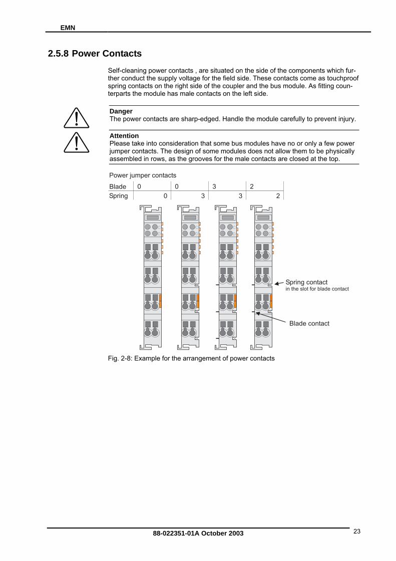
2.5.8 Power Contacts
Self-cleaning power contacts , are situated on the side of the components which fur-ther conduct the supply voltage for the field side. These contacts come as touchproof
spring contacts on the right side of the coupler and the bus module. As fitting coun-terparts the module has male contacts on the left side.
Danger The power contacts are sharp-edged. Handle the module carefully to prevent injury.
Attention Please take into consideration that some bus modules have no or only a few power jumper contacts. The design of some modules does not allow them to be physically assembled in rows, as the grooves for the male contacts are closed at the top.
Fig. 2-8: Example for the arrangement of power contacts
88-022351-01A October 2003 23

PIO Parker I/O-System
2.5.9 Wire connection
components have CAGE CLAMP® connections. All
The CAGE CLAMP® connection is appropriate for solid, stranded and fine–stranded conductors. Each clamping unit accommodates one conductor.
Fig. 2-9: CAGE CLAMP® Connection
The operating tool is inserted into the opening above the connection. This opens the CAGE CLAMP®. Subsequently the conductor can be inserted into the opening. After removing the operating tool, the conductor is safely clamped.
More than one conductor per connection is not phave to be made at one connection point, then they should be made away from the connection point using Terminal Blocks. The terminal blocks may be jumpered to-gether and a single wire brought back to the I/O module connection point.
ermissible. If several conductors
AttentionIf it is unavoidable to jointly connect 2 conductors, then a ferrule must be used to join the wires together. Ferrule: Length 8 mm Nominal cross sectionmax. 1 mm2 for 2 conductors with 0.5 mm2 each
88-022351-01A October 2003 24

EMN
2.6 Power Supply
2.6.1 Isolation
• Electronics of the couplers and the bus modules (internal bus).
• All bus modules have an electrical isolation between the electronics (internal bus,
Within the fieldbus node, there are three electrically isolated potentials.
• Operational voltage for the fieldbus interface.
logic) and the field electronics. Some analog input modules have each channel electrically isolated, please see catalog.
Fig. 2-10: Isolation
Attention The ground wire connection must be present in each group. In order that all protec-tive conductor functions are maintained under all circumstances, it is recommended that a ground wire be connected at the beginning and end of a potential group. (ring format, please see chapter "Grounding Protection"). Thus, if a bus module comes loose from a composite during servicing, then the protective conductor connection is still guaranteed for all connected field devices. When using a joint power supply unit for the 24 V I/O-system supply and the 24 V field supply, the electrical isolation between the internal bus and the field level is eliminated for the potential group.
88-022351-01A October 2003 25

PIO Parker I/O-System
2.6.2 I/O-system Supply
Connection
V direower supply is provided via the
The I/O-SYSTEM requires a 24The pThe voltage supply is reverse voltage protected.
ct current I/O-system supply (-15% or +20 %). coupler.
Fig. 2-11: I/O-system Supply
voltage). The 5 V I/O-system voltage is electrically connected to the 24 V I/O-system supply.
Alignment
Recommendation
The direct current supplies all internal I/O-system components, e.g. coupler electron-ics, fieldbus interface and bus modules via the internal bus (5 V I/O-system
A stable network supply cannot be taken for granted always and everywhere. There-fore, regulated power supply units should be used in order to guarantee the quality of the supply voltage. The sp
upply capacity of the from the technical data of the com-onents.
coupler can be taken
88-022351-01A October 2003 26
EMN
Internal current consumption*) Current consumption via I/O-system voltage:
5 V for electronics of the bus modules and coupler
Residual current for bus termi-nals*)
Available current for the bus modules. See coupler and internal I/O-system.
Example Coupler PIO-337:
sum I(5V) total : 2000 mA at 5V The internal current consumption is indicated in the technical data for each bus ter-minal. In order to determine the overall requirement, add together the values of all
ut modules (PIO-530).
400 mA
dules.
I(5 V) total = Sum of all the internal current consumption of the con-nected bus modules + internal current consumption coupler
I(5 V) total = Sum of all the internal current consumption of the con-nected bus modules
Input current I(24 V) = 5 V / 24 V * I(5 V) total / η
η = 0.87 (at nominal load)
internal current consumption:350 mA at 5V residual current for bus modules:1650 mA at 5V
bus modules in the node.
Example: A node with a CANopen Coupler PIO-337 consists of 24 digital input modules (PIO-430) and 16 digital outp
Current consumption: 24*17 mA = 408 mA 16*25 mA = Sum = 808 mA
The coupler can provide 808 mA (max. 1650 mA) for the bus mo
The maximum input current of the 24 V I/O-system supply is 500 mA. The exact elec-trical consumption (I(24 V)) can be determined with the following formulas:
Coupler
Note If the electrical consumption of the power supply point for the 24 V-I/O-system sup-ply exceeds 500 mA, then the cause may be an improperly aligned node or a defect.During the test, all outputs must be active.
88-022351-01A October 2003 27
PIO Parker I/O-System
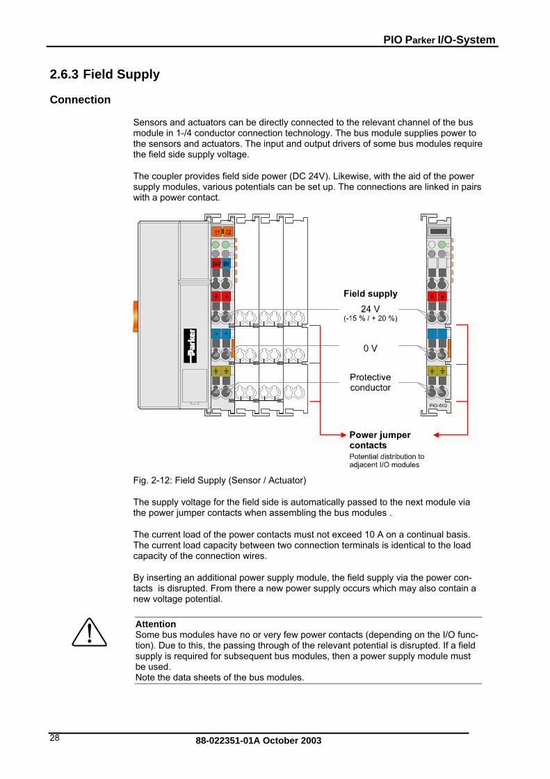
2.6.3 Field Supply
Connection
Sensors and actuators can be directly connected to the relevant channel of the bus ctor connection technology. The bus module supplies power to module in 1-/4 condu
the sensors and actuators. The input and output drivers of some bus modules require the field side supply voltage.
The coupler provides field side power (DC 24V). Likewise, with the aid of the power supply modules, various potentials can be set up. The connections are linked in pairs with a power contact.
PIO
Fig. 2-12: Field Supply (Sensor / Actuator)
The supply voltage for the field side is automatically passed to the next module via wer jumper contacts when assembling the bus modules .
new voltage potential.
the po
The current load of the power contacts must not exceed 10 A on a continual basis. The current load capacity between two connection terminals is identical to the load capacity of the connection wires.
By inserting an additional power supply module, the field supply via the power con-tacts is disrupted. From there a new power supply occurs which may also contain a
Attention Some bus modules have no or very few power contacts (depending on the I/O func-tion). Due to this, the passing through of the relevant potential is disrupted. If a field supply is required for subsequent bus modules, then a power supply module must be used. Note the data sheets of the bus modules.
88-022351-01A October 2003 28
EMN
2.6.4 Power Supply Unit
The I/O-SYSTEM requires a 24 V direct current I/O-system supply with a maximum deviation of -15% or +20 %.
Recommendation A stable network supply cannot be taken for granted always and everywhere. There-
units should be used in order to guarantee the quality fore, regulated power supply of the supply voltage. A buffer (20I/O-system buffers for approx 1 ms.
The electrical requirement for the fie
0 µF per 1 A current load) should be provided for brief voltage dips. The
ld supply is to be determined individually for each ower supply point. Thereby all loads through the field devices and bus modules hould be considered. The field supply as well influences the bus modules, as the in-
puts and outputs of some bus modules require the voltage of the field supply.
ps
Note The I/O-system supply and the field supply should be isolated from the power sup-plies in order to ensure bus operation in the event of short circuits on the actuator side.
2.7 Grounding
2.7.1 Grounding the DIN Rail
Framework Assembly
When setting up the framework, the carrier rail must be screwed together with the electrically conducting cabinet or housing frame. The framework or the housing must be grounded. The electronic connection is established via the screw. Thus, the car-rier rail is grounded.
Attention Care must be taken to ensure the flawless electrical connection between the carrier rail and the frame or housing in order to guarantee sufficient grounding.
Insulated Assembly
Insulated assembly has been achieved when there is constructively no direct conduc-tion connection between the cabinet frame or machine parts and the carrier rail. Here the earth must be set up via an electrical conductor.
The connected grounding conductor should have a cross section of at least 4 mm2.
Recommendation The optimal insulated setup is a metallic assembly plate with grounding connection with an electrical conductive link with the carrier rail.
88-022351-01A October 2003 29

PIO Parker I/O-System
2.7.2 Grounding Function
The grounding function increases the resistance against disturbances from electro-magnetic interferences. Some components in the I/O-system have a carrier rail con-tact that dissipates electro-magnetic disturbances to the carrier rail.
PIO
Fig. 2-13: Carrier rail contact
Attention Care must be taken to ensure the direct electrical connection between the carrier rail contact and the carrier rail. The carrier rail must be grounded.
88-022351-01A October 2003 30
EMN
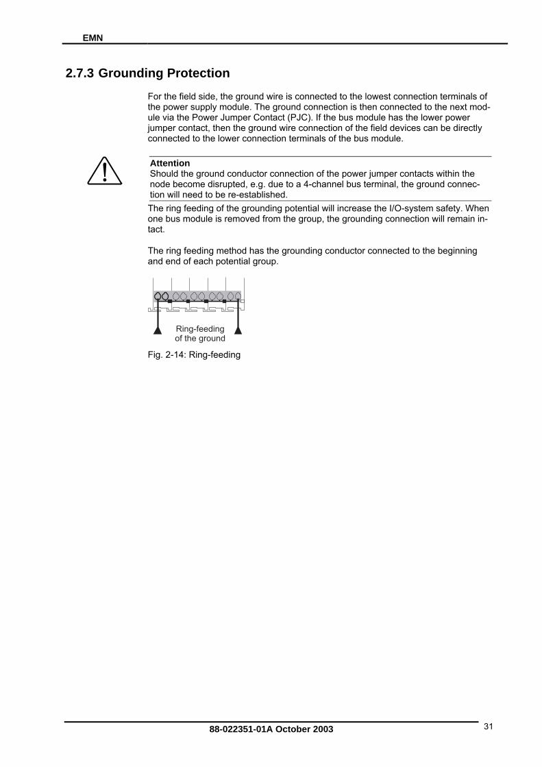
2.7.3 Grounding Protection
Fth
or the field side, the ground wire is connected to the lowest connection terminals of e power supply module. The ground connection is then connected to the next mod-
ule via the Power Jumper Contact (PJC). If the bus module has the lower power jumper contact, then the ground wire connection of the field devices can be directly connected to the lower connection terminals of the bus module.
Attention Should the ground conductor connection of the power jumper contacts within the node become disrupted, e.g. due to a 4-channel bus terminal, the ground connec-tion will need to be re-established. The ring feeding of the grounding potential will increase the I/O-system safety. When one bus module is removed from the group, the grounding connection will remain in-tact.
The ring feeding method has the grounding conductor connected to the beginning h potential group. and end of eac
Fig. 2-14: Ring-feeding
88-022351-01A October 2003 31

PIO Parker I/O-System
2.8 Shielding (Screening)
a and signal conductors reduces electromagnetic interfer-y. Measurement errors, data transmission
2.8.1 General
The shielding of the datences thereby increasing the signal qualiterrors and even disturbances caused by overvoltage can be avoided.
Attention Constant shielding is absolutely required in order to ensure the technical specifica-tions in terms of the measurement accuracy. The data and signal conductors should be separated from all high-voltage cables. The cable shield should be potential. With this, incoming disturbances can be easily diverted. The shielding should be placed over the entrance of the cabinet or housing in order to already repel disturbances at the entrance.
2.8.2 Bus Conductors
The shielding of the bus conductor is described in the relevant assembly guideline of the bus I/O-system.
2.8.3 Signal Conductors
Bus modules for most analog signals along with many of the interface bus modules include a connection for the shield.
2.9 Assembly Guidelines / Standards DIN 60204, Electrical equipping of machines
DIN EN 50178 Equipping of high-voltage I/O-systems with electronic components (replacement for VDE 0160)
EN 60439 Low voltage – switch box combinations
88-022351-01A October 2003 32
EMN
3 Fieldbus coupler 3.1 Fieldbus coupler
34
.41 ....................................................................42
3.1.5 Data exchange...............................................................................................42 8
...54 58
This chapter includes:
3.1.1 Description .....................................................................................................3.1.2 Hardware .......................................................................................................35 3.1.3 Operating System .........................................................................................3.1.4 Process Image...........................
3.1.6 Starting up CANopen fieldbus nodes ............................................................43.1.7 LED display.................................................................................................3.1.8 Technical Data ...............................................................................................
88-022351-01A October 2003 33

PIO Parker I/O-System
3.1.1 Description
The fieldbus coupler displays the peripheral data of all I/O modules in the I/O-SYSTEM on CANopen. The data is transmitted with PDOs and SDOs.
In the initialization phase, the bus coupler determines the physical structure of the node and creates a process image from this with all inputs and outputs. This could involve a mixed arrangement of analog (word by word data exchange) and digital (byte by byte data exchange) modules.
The local process image is subdivided into an input and output data area. The proc-ess data can be read in via the CANopen bus and further processed in a control I/O-system. The process output data is sent via the CANopen bus. The data of the analog modules are mapped into the PDOs according to the order of their position downstream of the bus coupler. The bits of the digital modules are compiled to form bytes and also mapped into PDOs. Should the number of digital I/Os exceed 8 bits, the coupler automatically starts another byte.
The entries in the object directory can be mapped to the 32 RxPDOs and 32 TxPDOs as required. The entire input and output data area can be transmitted with the SDOs.
“Spacer modules” can be set using the software.
88-022351-01A October 2003 34

EMN
3.1.2 Hardware
View
Fig. 3-1: Fieldbus coupler CANopen
The fieldbus coupler is comprised of:
• Supply module with Internal I/O-system supply module for the I/O-system supply as well as power jumper contacts for the field supply via I/O module assemblies.
• Fieldbus interface with the bus connection
• DIP switch for baud rate and node ID
• Display elements (LEDs) for status display of the operation, the bus communication, the operating voltages as well as for fault messages and diagnosis
• Configuration Interface
• Electronics for communication with the I/O modules (internal bus) and the fieldbus interface
88-022351-01A October 2003 35

PIO Parker I/O-System
Device supply
The supply is made via terminal bocks with CAGE CLAMP® connection. The device supply is intended both for the I/O-system and the field units.
1
2
3
4
5
6
7
8
24V
10nF
24V
10nF
0V
DC24V/0V
24V
0V
0V
DCI/O
modules
ElectronicFieldbusInterface
PIO-337
o
The fieldbus interface is supplied with electrically isolated voltage from the internal I/O-system supply module.
Fig. 3-2: Device supply
The integrated internal I/O-system supply module generates the necessary voltage tsupply the electronics and the connected I/O modules.
88-022351-01A October 2003 36

EMN
Fieldbus connection
The connection point is lowered in such a way that after a connector is inserted, in-stallation in an 80 mm high switchbox is possible.
een the fieldbus I/O-system and the electronics is made via the DC/DC converter and the optocoupler in the fieldbus.
The CAN interface is designed as an open style connection.
The electrical isolation betw
Pin Signal Description
1 Not used
2 CAN_H CAN Signal High
3 Drain, Shield
Shield connection
4 CAN_L CAN Signal Low
FieldbusconnectionSeries 231(MCS)
CAN_High
drain
CAN_Low
CAN_GND
5 GND Ground
Fig. 3-3: Fieldbus connection, MCS
If a shield exists, it can b via a 1 MΩ re-istor to ground (earth) (rail carrier contact). A connection of low impedance between
shield and ground (earth) can only be made externally (for example by a supply ter-minal block). It is recommended to have a central ground (earth) contact for the whole CANbus shield.
e connected to drain. The shield is connecteds
88-022351-01A October 2003 37

PIO Parker I/O-System
Display elements
The operating condition of the fieldbus coupler or node is signalled via light diodes (LED).
24V 24V0V 0V
+ ++ +
STOP
RUN
TX
I/O
CANopen CANopen
C C
D DB B
A A
RXOVERFLOW
STOP
RUN
TX
RXOVERFLOW
I/O I/O
C A
A B
Fig. 3-4:Display elements
LED Color Meaning
STOP Red The buscoupler / node is in the state STOP
RUN Green The buscoupler / node is in the state OPERATIONAL
Tx- Red CAN transOverflow
mitter buffer is full.
Rx- Red CAN receiver buffer is full. Overflow
IO red / green / orange
The 'I/O'-LED indicates the operation of the node and signals faults encountered.
-
A green Status of the operating voltage I/O-system
B or C green Status of the operating voltage – power jum(LED position is manufacturing dependent)
per contacts
88-022351-01A October 2003 38

EMN
Configuration interface
-d the cover flap.
The configuration interface used for the communication or for firmware transfer is located behin
openflap
Configurationinterface Fig. 3-5: Configuration interface
Hardware address (Module ID)
The DIP switch is used both for setting the baud rate of the fieldbus coupler and for setting the module ID. This module ID is necessary for calculating the COB IDs (i.e. of PDO1...4, 1. Server SDO, etc.).
12
34
5
45
ON
ON1
23
6 67
8
78 Fig. 3-6: f atio d dd
The binary significance of the individual DIP switches increases according to the nu e m ule 1 i et b DIP ON the du D 8
IP4 = O
The nodes of the I/O-SYSTEM can have module IDs from 1 to 127.
Setting o st n (no e) a ress
switch mber, i.e. th od ID s s y 1 = , mo le I by D N, etc.
88-022351-01A October 2003 39

PIO Parker I/O-System
Setting the baud rate
The bus coupler supports 9 different Baud rates. DIP switches are used to set the baud rate.
The bus coupler changes to the configuration mode using the set module ID = 0 (all DIP switches off) with subsequent power On. The current set baud rate is displayed in this status. The baud rate display is shown by the top LED group (STOP, RUN, Tx-, Rx-Overflow), whereby STOP = Switch 1, RUN = Switch 2, Tx-Overflow = Switch 3 and Rx-Overflow = Switch 4. The current
w es
he set configuration is saved by turning DIP8 to 'ON'. Following saving, the new LEDs having a steady light. Except for
the baud rate of 1MBaud, this is displayed by all 4 LEDs blinking/being lit.
Overflow LED blink / are lit 250 kB: STOP and RUN LED blink / are lit
set baud rate is displayed by the corresponding LEDs blinking slowly. Now the nebaud rate can be set using the DIP switch, by turning the corresponding DIP switchto 'ON'.
Tbaud rate is displayed by the corresponding
Example: 125 kB: Tx-
12
34
5
ON
67
8
12345678
ON
Fig. 3-7: Example: Saving the baud rate 125 kB
In this status no data exchange via CAN is possible.
DIP Function 1 Mbit
800 kB
500 kB
250 kB
125 kB
100 kB
50 kB
20 kB
10 kB
is dis-played by LED
1 (LSB) Baud rate 0 1 0 1 0 1 0 1 0 STOP 2 Baud rate 0 0 1 1 0 0 1 1 0 RUN 3 Baud rate 0 0 0 0 1 1 1 1 0 Tx-
Overflow 4 (MSB) Baud rate 0 0 0 0 0 0 0 0 1 Rx-
Overflow 5 6 7 8 Accept-
ance ´off´ -> ´on´ : Accepting the configuration settings
Once the baud rate setting / baud rate check is completed, switch off the operating voltage knowing that only the DIP value will be used to calculate the IDs which has been set during power ON. When switched off, the desired module ID (=1 as deliv-ered) can be set on the DIP.
Default baud rate: 125 kB
88-022351-01A October 2003 40
EMN
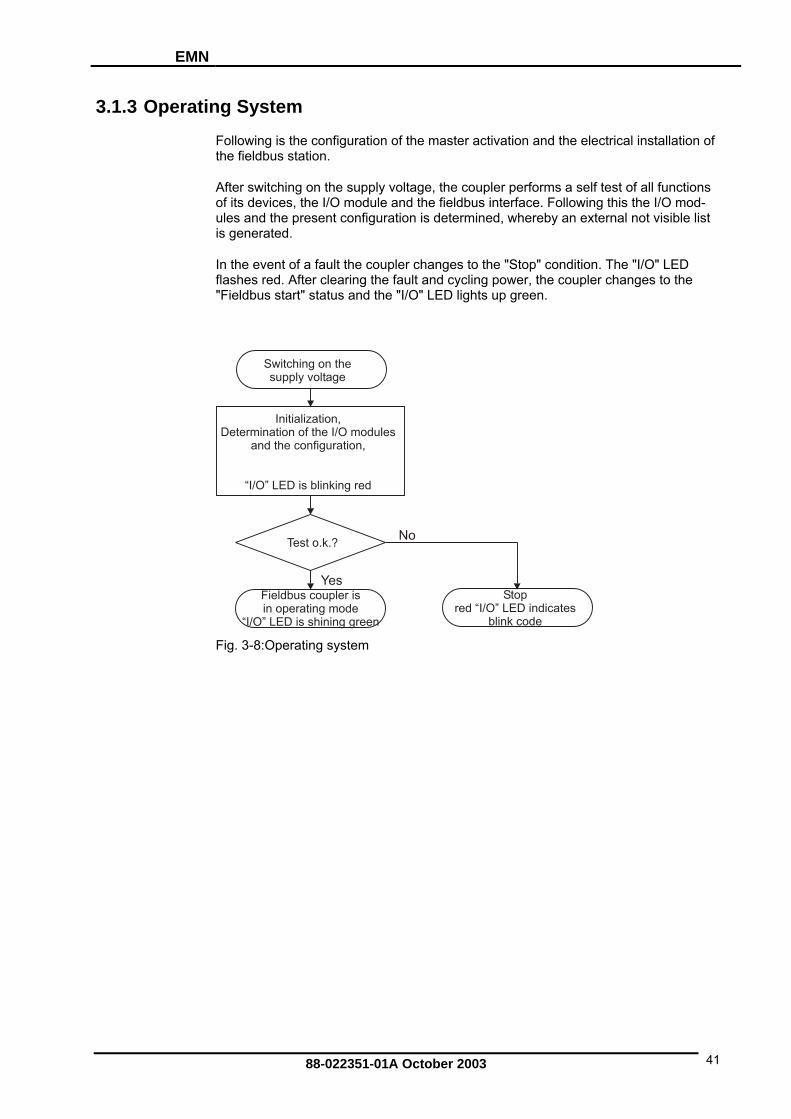
3.1.3 Operating System
n of
After switching on the supply voltage, the coupler performs a self test of all functions
Following is the configuration of the master activation and the electrical installatiothe fieldbus station.
of its devices, the I/O module and the fieldbus interface. Following this the I/O mod-ules and the present configuration is determined, whereby an external not visible list is generated.
In the event of a fault the coupler changes to the "Stop" condition. The "I/O" LED flashes red. After clearing the fault and cycling power, the coupler changes to the"Fieldbus start" status and the "I/O" LED lights up green.
StopYes
Fieldbus coupler isred “I/O” LED indicates
blink code
Switching on the
Test o.k.?No
in operating mode“I/O” LED is shining green
rating system
supply voltage
Initialization,Determination of the I/O modules
and the configuration,
“I/O” LED is blinking red
Fig. 3-8:Ope
88-022351-01A October 2003 41

PIO Parker I/O-System
3.1.4 Process Image
After powering up, the coupler recognizes all I/O modules plugged into the node which supply or wait for data (data width/bit width > 0). In the nodes analog and digi-
n be mixed.
The coupler produces an internal process image from the data width and the type of l as the position of the I/O modules in the node. It is divided into an
inpu
e al I/O modules is bit orientated, i.e. the data exchange is made bit for where the data exchange is made byte for byte. These I/O modules include for ex-
les for angle and path measurement as well as the
tal I/O modules ca
I/O module as welt and an output data area.
Th data of the digitbit. The analog I/O modules are all byte orientated I/O modules, i.e. modules
ample the counter modules, I/O moducommunication modules.
Note For the number of input and output bits or bytes of the individual I/O modules please
le description. refer to the corresponding I/O modu
The data of the I/O modules is separated for the local input and output process image in the sequence of their position after the coupler in the individual process image. In the respective I/O area, first of all analog modules are mapped, then all digital
odules, even if the order of the connected analog and digital modules does not nnels are grouped, each of these groups hav-
of 1 byte. Should the number of digital I/Os exceed 8 bits, the cou-lly starts another byte.
mcomply with this order. The digital chaing a data widthpler automatica
Note A rocess image restructuring may result ip f a node is changed or extended. In this case the process data addresses also change in comparison with earlier ones. In the
e cess data of all previous modules into ac-count. ev nt of adding a module, take the pro
change 3.1.5 Data ex
With CANopen, the transmission of data, the triggering of events, the signalling of error states etc. is made using communication objects. Each communication object is assigned a unique COB-ID (Communication Object Identifier) in the network.
Parameters for the communication objects as well as parameters and data of the CANopen subscribers are filled in an object directory().
88-022351-01A October 2003 42

EMN
Communication objects
for process data exchange of fieldbus node input data
• 32 Rx-PDOs, for process data exchange of fieldbus node output data
• 2 Server SDO, for exchange of configuration data and for information on the state of the node
• Synchronization Object (SYNC), for network synchronisation
• Emergency Object (EMCY)
• Network Management Objects - Module Control Protocols - Error Control Protocols - Bootup Protocol
Communication interfaces
For a data exchange, the CANopen fieldbus coupler is equipped with two interfaces:
• the interface to fieldbus (-master) and
• the interface to the bus modules.
The fieldbus coupler supports the following communication objects:
• 32 Tx-PDOs,
Data exchange takes place between the fieldbus master and the bus modules. Access from the fieldbus side is fieldbus specific.
88-022351-01A October 2003 43

PIO Parker I/O-System
Memory areas
.
The coupler uses a memory space of 256 words (word 0 ... 255) for the physical input and output data. The division of the memory spaces is identical with all PARKER fieldbus couplers
fieldbus coupler
I O
1
2
memory areafor input data
I/O modules
inputmodules
word 255
memory areafor output data
outputmodules
word 0
word 0
fieldbus
Fig. 3-9: Memory areas and data exchange for a fieldbus coupler
The coupler process image contains the physical data of the bus modules in a storage area for input data and in a storage area ord 0 ... 255 each).
1
2 In the same manner, writing to the output modules is possible from the fieldbus de.
word 255
for output data (w
The input module data can be read from the fieldbus side.
si
88-022351-01A October 2003 44

EMN
Addressing
e supply voltage, the data is mapped from the process image to itialization). A CANop us master uses bit indexes
or access purposes. n of the data in the pro age has no dir ning for the
Upon switching on than object directory (in en fieldb the 16and 8 bit sub-indexes of the object directory in order to address the data via the PDOs or SDOs and fTherefore, the positio cess im ect meaCANopen user.
fieldbus coupler
I O
P
1
DO
SDO
2
.
word 255
.
.
Index
for input dataI/O modules
inputmodules
outputmodules
ldbusaster
memory areafor output data
Fig. 3-10: Fieldbus specific data exchange for a CANopen fieldbus coupler
Indexing the bu
rently connected module configuration coincides with the configuration stored before, initialization takes place with this configuration.
IndexSub-
memory area
word 0
Object directory()
fiem
word 0
word 255
s module data
If a customer specific configuration was stored prior to the initialization, and if the cur-
Note For an example for the initialization of the refer to chapter 3.1.6 "Starting up CANo
customer specific configuration, please pen fieldbus nodes".
In every other case, when initializing, the object direfiguration according to the device profile DS 401.
The entry into the object directory is then made separately according to data width (1 bit, 1 byte, 2 by
ctory is assigned a default con-
tes, 3 bytes, etc...) and input and output. The physical bus module arrangement within a node is optional.
Data width = 1 Word / channel Data width = 1 Bit / channel
Analog inpu s Digital input modulet module s Analog outp odul Digital output moduut m es les
Table 3-1 O m: I/ odule data width
88-022351-01A October 2003 45
PIO Parker I/O-System
Note For the number of input and output bits or bytes of the individual I/O modules please
the es /O module description. refer to corr ponding I
ita odu .g t CA l module data is
digital input data to
he assignment of bus module data of a data width of 1 byte or more is made in rela-
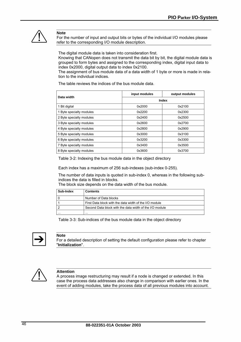
The table reviews the indices of the bus module data.
input modules output modules
The digKnowin
l m le data is taken into consideration firstNopen does not transmit the data bit b
tha y bit, the digita
grouped to form bytes and assigned to the corresponding index, dex 0x2000, digital output data to index 0x2100. in
Ttion to the individual indices.
Data width Index
1 Bit digital 0x2000 0 0x210
1 Byte speci mod 0x2200 0 alty ules 0x230
2 Byte specialty mod 0x2400 0 ules 0x250
3 Byte specialty mod 0x2600 ules 0x2700
4 Byte specialty modules 0x2800 0x2900
5 Byte specialty modules 0x3000 0x3100
6 Byte specialty modules 0x3200 0x3300
7 Byte specialty modules 0x3400 0x3500
8 Byte specialty modules 0x3600 0x3700
Table 3-2: Indexing the bus module data in the object directory
Each index has a maximum of 256 sub-indexes (sub-index 0-255).
The number of data inputs is quoted in sub-index 0, whereas in the following sub-indices the data is filled in blocks. The block size depends on the data width of the bus module. Sub-Index Contents 0 Number of Data blocks 1 First Data block with the data width of the I/O module 2 Second Data block with the data width of the I/O module ... ...
Table 3-3: Sub-indices of the bus module data in the object directory
Note For a detailed description of setting the default configuration please refer to chapter "Initialization".
Attention A process image restructuring may result if a node is changed or extended. In this case the process data addresses also change in comparison with earlier ones. In the event of adding modules, take the process data of all previous modules into account.
88-022351-01A October 2003 46

EMN
Example: The bus module configuration contains : 1) 5 digital 2 channel input modules (i.e. PIO-402), 2) one digital 4 channel output module (i.e. PIO-504) and 3) two 2 channel analog output modules with output modules having 2 bytes per chan-
-552).
el input modules:
Description:
nel (i.e. PIO
To 1) Index the data of the 5 digital 2 chann
Index: Sub- Contents: Index: 0 2 number of dig. 8 Bit input blocks 1 D4.2 D4.1 D3.2 D3.1 D2.2 D2.1 D1.2 1. dig. input block
D1.1 *)0x2000 2 0 0 0
D5.1 * 0 0 0 D5.2 2. dig. input block
)
*) D1.1 = Data bit module 1 channel 1, D1.2 = Data bit module 1channel 2, etc.
To 2) Index the data of the digital 4 channel output module:
Index: Sub- Contents: Index:
Description:
0 1 number of dig. 8 Bit input blocks 0x2100 1 0 0
* 0 0 D1.4 D1.3 D1.2 D1.1 dig. output block
) * D1.1 = Data bit module 1 channel 1, D1.2 = Data bit module 1 channel 2, etc. )
To 3) Index the data of the 2 analog 2 channel output modules:
Index: Sub-Index:
Contents: Description:
0 4 number of 2 Byte specialty chan-nels
1 D1.1 *) 1. output channel 2 D1.2 * 2. output channel )
3 D2.1 *) 3. output channel
0x2900
4 D2.2 *
4. output channel )
*) D1.1 = Data word module 1 channel 1, D1.2 = Data word module 1 channel 2, etc.
88-022351-01A October 2003 47
PIO Parker I/O-System
3.1.6 Starting up CANopen fieldbus nodes
This chapter shows the step-by-step procedure for starting up a CANopen fieldbus node.
Attention This description is given as an example and is limited to the execution of a local start-up of an individual CANopen fieldbus node.
The procedure contains the following steps:
ting the PC and fieldbus node
5. Releasing the analog input data . pplication specific mapping
Connecting the
Checking and s
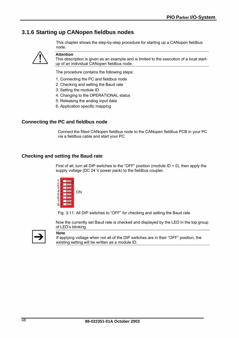
F t of all, turn all DIP ss
1. Connec2. Checking and setting the Baud rate 3. Setting the module ID 4. Changing to the OPERATIONAL status
6 A
PC and fieldbus node
Connect the fitted CANopen fieldbus node to the CANopen fieldbus PCB in your PC via a fieldbus cable and start your PC.
etting the Baud rate
irs witches to the “OFF” position (module ID = 0), then apply the upply voltage (DC 24 V power pack) to the fieldbus coupler.
12
ON1
23 3
44 ON56
567
78
8 FF” for checking and setting the Baud rate
Now the currently set Baud rate is checked and displayed by the LED in the top group o
Fig. 3-11: All DIP switches to “O
f LED’s blinking.
Note If applying voltage when not all of the DIP switches are in their “OFF” position, the existing setting will be written as a module ID.
88-022351-01A October 2003 48

EMN
Now push the correspondini.e. DIP switch 3 for the Baud rate 125 k
g DIP switches to the desired Baud rate to 'ON', B.
12
34
5
ON
67
8
ON
12345678
Fig. 3-12: Setting the Baud rate 125 kB
TT
o be able to store the new setting, push DIP switch 8 also to 'ON'. hen switch off the coupler supply voltage.
12
34
5
ON
67
8
12345678
ON
Fig. 3-13: Storing the Baud rate 125 kB
Setting the module ID
The module ID is set with the supply voltage isolated. For this purpose, push all DIP switches to their “OFF” position again. Then push the DIP switch intended for the de-sired module ID to “ON”, i.e. DIP switch 1 for the module ID 1.
12
34
5
ON
67
8
12345678
ON
Fig. 3-14: Setting the module ID 1
As soon as you switch on the supply voltage, the coupler is in the INITIALIZATION status. At the same time, the process image is created by means of the connected bus mod-ules and the object directory initialized following the default mapping, if no application specific configuration was stored. After a fault-free termination of the initialization phase, the coupler automatically changes to the PRE-OPERATIONAL status. In this status, communication is possible via SDOs, which you can now use to pro-ceed with various settings via your CAN Master software:
• You can set the coupler directly to its OPERATIONAL status.
Note Due to the fact that as a default setting, the PDO transmission of the analog input data is switched off, the analog input data will not be taken into consideration.
• You can release the switched off transmission of the analog input data or • select an application specific mapping.
88-022351-01A October 2003 49

PIO Parker I/O-System
Changing to the OPERATIONAL status
mand from the network management ob-
You can change the coupler PRE-OPERATIONAL status to the OPERATIONAL status using the Start_Remote_Node comjects. This creates the communication readiness of the fieldbus node for PDOs (see chapter "Start Remote Node").
Note As a default setting, the PDO transmission of the analog input data is switched off. For this reason, this data is read out only once and subsequently never updated. To be able to use this data via the PDOs, switch the analog input data on in the PRE-
OPERATIONAL status. Access via the SDOs is possible at any time.
rational. Communication is possible r "Initialization").
Switching on the analog input data
To avoid the CAN bus from overflowing with CAN messages, the transmission of analog input data via PDOs is deactivated in the default setting. This means that ob-ject 0x6423 "Analoge Input Global Interrupt e 'FALSE' (= '0') ( apter "O t 0x6423, Analo able").
') value. Subs ode" command can be used to change the cou-pler status from PRE-OPERATIONAL to OPERATIONAL. This process allows com-munication via PDOs and the transmission of analog input data.
If no further settings are made, the coupler is operational and communication can oc-cur a to the D t Mapping (refer
If no further settings are made, the coupler is opeaccording to the Default-Mapping (refer to chapte
Enable" has the default valug Input Global Interrupt Enrefer to ch bjec
When the coupler has the PRE-OPERATIONAL status, you can generally release the transmission by setting the object 0x6423 to the TRUE (= '1
equently, the "Start Remote N
ccording efaul to chapter "Initialization").
88-022351-01A October 2003 50

EMN
Application specific mapping
An alternative to the use of the default mapping is to define the data to be transmitted by has to
Details of how to proceed with an application specific mapping are explained below.
ExaThe annel and the first 8 bit digital input group are to be read using the TxPDO 2. For transmission purposes, the CAN identifier 0x432 is to be used. Transmission must be synchronous with each 3rd SYNC object.
The default CAN IDs are used for the SDOs. The setting is made at node 8.
xx... is not evaluated
1. First of all, deactivate the PDO you wish to map. In the present example, this is the TxPDO2.To this effect, write value 0x80000000 into the object having the index 0x1801, sub-index 01 (Transmit PDO Communication Parameter).
PDOs in an application specific PDO mapping. For this purpose, the coupler be in the PRE-OPERATIONAL status.
mple: 3rd and the 5th 2 byte analog input ch
Deactivating PDO:
CAN ID Data
Transmit 608 0x23 01 18 01 00 00 00 80
Receive 588 0x60 01 18 01 xx xx xx xx
2. Then deactivate the PDO mapping by zeroing the number of mapping objects in index 0x1A01, sub-index 0 (Transmit PDO Mapping Parameter).
Deactivating PDO mapping:
CAN ID Data
Transmit 608 0x2F 01 1A 00 00 xx xx xx
Receive 588 0x60 01 1A 00 xx xx xx xx
3. Enter into the TxPDO mapping parameter structure (Index 0x1A01) the Index, Sub-Index and the Object length of the application object. Max. 8 bytes of data can be assigned per PDO.
Writing into the mapping parameter structure:
Application object Index Sub-Index
3. analog input channel 0x2400 3
5. analog input channel 0x2400 5
1. digital input group 0x2000 1
The following structure must be reached in the mapping parameters of the 2nd TxPDO in order to ens k set: ure the tas
TxPDO Mapping Parameter Structure, Index 0x1A01
Application object
Sub-Index: Index: Sub-Index: Object length in Bit
0 3
1 0x2400 3 0x10
2 0x2400 5 0x10
3 0x2000 1 0x08
88-022351-01A October 2003 51

PIO Parker I/O-System
Note First of all enter the mapping parameter s 1 ... 8 in the sub-index 0,
wed by the nu valid sub-indexub-index
follo mber of es. These objects are stored with the aid of SDO transmissions:
Mapping 3. analog input channel
CAN ID Data
Transmit 0x608 0x23 01 1A 01 10 03 00 24 2 data bytes invalid 011A Index(Lowbyte first) 01 g channel 0 rd analog channel is in the manufacturer device profile
t) where the 3rd
device profile
3 0
1 Sub-index 0 Data width of the analo3 Sub-index, where the 3
00 24Index (Lowbyte firsanalog channel is in the manufacturer
Receive 0x588 06001 Sub-Index
x60 01 1A 01 xx xx xx xx 0 OK 11A Index (Lowbyte first)
Mapping 5. analog input channel
CAN ID Data
Transmit 0x608 0x23 01 1A 02 10 05 00 24
Receive 0x588 0x60 01 1A 02 xx xx xx xx
Mapping 1. digital input group
CAN ID Data
Transmit 0x608 0x23 01 1A 03 08 01 00 20
Receive 0x588 0x60 01 1A 03 xx xx xx xx
Number of mapping objects = 3, enter on Sub-Index 0
CAN ID Data
Transmit 0x608 0x2F 01 1A 00 03 xx xx xx
Receive 0x588 0x60 01 1A 00 xx xx xx xx
4. Now write into the object with Index 0x1801, Sub-Index 1 to 3 (Transmit PDO Communication Parameter) the communication parameters in the structure. Thereby the Transmission Type is 3 ( Synchronous transmission with every 3. SYNC object).
Enter the Communication Parameter:
TxPDO Communication Parameter, Index 0x1801
88-022351-01A October 2003 52

EMN
Sub-Index: Value: Meaning:
0 3 Number of supported entries in the record
1 0x432 COB-ID used by PDO
2 3 Transmission Type
3 0 Inhibit Time
Sub-Index 3: Inhibit Time = 0
CAN ID Data
Transmit 0x608 0x2B 01 18 03 00 00 xx xx
Receive 0x588 0x60 01 18 03 xx xx xx xx
Sub-Index 2: Transmission Type = 3
CAN ID Data
Transmit 0x608 0x2F 01 18 02 03 xx xx xx
Receive 0x588 0x60 01 18 02 xx xx xx xx
Sub-Index 1: Change COB-ID = 432 on PDO and PDO from invalid to valid
CAN ID Data
Transmit 0x608 0x23 01 18 01 32 04 00 00
Receive 0x588 0x60 01 18 01 xx xx xx xx
5. When you change the bus coupler to OPERATIONAL using the ”Start Remote Node" message, the PDOs are activated and the TxPDO object can now be used for data transmission.
88-022351-01A October 2003 53

PIO Parker I/O-System
3.1.7 LED display
The coupler possesses several LEDs for on site display of the coupler operating status or the complete node.
CD
B
A
Fig. 3-15: Display elements
Here is a descriptionof the two LED groups.
The first group = fieldbus contains the solid colored eSTOP (red) RUN (green) Tx-Overflow (red) and Rx-Overflow (red), signalling the operating status of the communication via CAN.
The second group = module bus consists of the three-color I/O LED (red/green/orange). The m st e tiosignalled by this LED.
Blink code
Detailed fault messages are displayed with the aid of a blink code. A fault is cyclically displayed with up to 3 blink sequences.
• first b quenc approx. 10 z) starts th .
• The second blink sequence (approx. 1 Hz) following a pause. The number of blink pulses indicates the fault code.
• third sequenc (approx. 1 ) follows a au er pulses indicates the fault argument.
LEDs with the d notation
odule bus atus and th software excep n codes are
The link se e ( H e fault display
The blink e Hz fter a further p se. The numbof blink
88-022351-01A October 2003 54

EMN
Fieldbus status
The upper four LED´s (STOP, RUN, Tx- und Rx-Overflow) signal the operating condi-t the C mmions of AN co unication.
STOP RUN TXOVERF RXOVERF Meaning Remedy
OFF OFF OFF OFF No function or self-test
check supply (24V and 0V), wait for self-test
OFF SLOW FLASHING
X X Module is in the state PRE-OPERATIONAL
OFF ON X X Module is in the state OPERATIONAL
ON OFF X X Module is in the STOP state or fatal fieldbus independent error (i.e. a module was removed), incor-rect configuration
Check in the event of a fieldbus inde-pendent error, reset the node, check same in the event of a configu-ration error
X X X ON CAN receiver buffer is full. Data loss is likely.
Increase the time span between 2 protocols.
X X ON X CAN transmitter buffer is full. Data loss is likely.
Check the data sizes of the bus I/O-system. In-crease the trans-mit priority of the module.
X X FAST FLASHING in turns with RXOVERF
FAST FLASHING in turns with TXOVERF
CAN Controller exceeded the Warning Level, to many error mes-sages
Check baud rate and bus connec-tion, install min. 2 modules in the network.
OFF FAST FLASHING
X X Module is in the state PRE-OPERATIONAL, Sync/Guard Mes-sage/Heartbeat failed
Change into the state OPERATIONAL and restart Sync/Guard mes-sage/Heartbeat
FAST FLASHING
FAST FLASHING
X X Module is in the state OPERATIONAL, Sync/Guard Mes-sage/Heartbeat failed
Restart Sync/Guard mes-sage/Heartbeat
FAST FLASHING
OFF X X Module is in the state STOP, Sync/Guard Mes-sage/Heartbeat failed
Change into the state OPERATIONAL and restart Sync/Guard mes-sage/Heartbeat
88-022351-01A October 2003 55
PIO Parker I/O-System
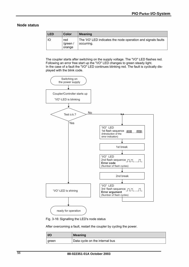
Node status
LED Color Meaning
IO red /green / orange
on and signals faults
The 'I/O' LED indicates the node operatioccurring.
The coupler starts after switching on the supply voltage. The "I/O" LED flashes red. D changes to green steady light.
In the case of a fault the "I/O" LED continues blinking red. The fault is cyclically dis-played with the blink c
Following an error free start up the "I/O" LE
ode.
“I/O”-LED is blinking
Test o.k.?
Yes
re opera
No
“I/O”-LED is shining
ady for tion
2nd break
1st break
“I/O” LED1st flash sequence(Introduction of theerror indication)
Error codeof flash cycles)
Coupler/Controller
t power sup
F
fter overcoming a fault, restart the coupler by cycling the power.
“I/O” LED2nd flash sequence
(Number
“I/O” LED3rd flash sequenceError argument(Number of flash cycles)
starts up
Switching onhe ply
ig. 3-16: Signalling the LED's node status
A
I/O Meaning
green Data cycle on the internal bus
88-022351-01A October 2003 56
EMN
off No data cycle on the internal bus
red Coupler hardware defective
red When starting: internal bus is initialized blinks During operation: general internal bus fault
red blinks cyclically
Fault message during internal bus reset and internal fault:
link code of the I/O LED Fault message via the b
Fault argument Fault description
Fault code w 1: Hard are and configuration fault
0 E rea o
EPROM check sum fault / check sum fault in parameter af the flash memory
1 Overflow of the internal buffer memory for the inline code
2 Unknown data type
3 Module type of the flash program memory could not be de-termined / is incorrect
4 Fault during writing in the flash memory
5 Fault when deleting the FLASH memory
6 Changed I/O module configuration found after AUTORESET
7 Fault when writing in the serial EEPROM
8 Invalid firmware
Fault code 2: Fault in programmed configuration
0 Incorrect table entry
Fault code 3: Internal bus command fault
0 I/O module(s) hrrect
as (have) identified internal bus command as inco
Fault code 4: Internal bus data fault
0 Data fault on internal bus or Internal bus interruption on coupler
n* (n>0) Internal bus interrupted after I/O module n
Fault code 5: Register communica tion fault
n* Internal bus fault during register communication with the I/O module n
Fault code 7: I/O module not supported
n* I/O module not supported at position n
* The number of blink pulses (n) indicates the position of the I/O module. I/O modules without data are not counted (i.e. supply module without diagnosis)
Example: the 13th I/O module is removed.
1. The "I/O" LED generates a fault display with the first blink sequence (approx. 10 H )
88-022351-01A October 2003 57

PIO Parker I/O-System
10 Hz).
2. The first pause is follo"I/O" LED blinks four times
wed by th cond blink sequence (approx. 1 Hz). The and thus signals the fault code 4 (internal bus data
e se
fault).
3. The third blink sequence follows e. The "I/O ERR" LED blinks e times. The fault argumen t the internal bus is interrupted the 12th I/O module.
the second paustwelvafter
t 12 means tha
Supply voltage status
LED Color Meaning
A Green Status of the operating voltage – I/O-system
C Green Status of the operating voltage – power jumper contacts
There are two green LED’s in the cou on to display the supply volt-
supply to the field side, i.e. the power jumper contacts.
3.1.8 Techni
pler supply sectiage. The left LED (A) indicates the 24 V supply for the coupler. The right hand LED (C) signals the
cal Data
system data
Number of nodes 110
Transmission medium shielded Cu cable3 x 0,25 mm2
Max. length of bus line 40 m ... 1000 m (baud rate dependent / cable dependent)
Baud rate aud ... 1 MBaud 10 kB
Buscoupler connection e connector, series 231 (MCS) 305/010-000 is included
5-pole malfemale connector 231-
Standards and approvals
UL E198563, UL508 (applied for)
Conformity marking CE
Accessories
EDS files PIO-914
Miniature WSB quick marking system
88-022351-01A October 2003 58

EMN
Technical data
Max. number of I/O modules 64
Input process image max. 512 bytes
Output process image max. 512 bytes
No. of PDO 32 Tx / 32 Rx
No. of SDO 2 Server SDO
Communication profile DS-301 V4.0
Device profile DS-401, marginal check, edge-triggered PDOs, programmable error response
COB ID Distribution SDO, standard
Node ID Distribution DIP switches
Other CANopen Features NMT Slave, Minimum Boot-up, Variable PDO Mapping, Emergency Message, Life Guarding
Configuration via PC or PLC
Voltage supply DC 24 V (-15 % / + 20 %)
Input currentmax 500 mA at 24 V
Efficiency of the power supply 87%
Internal power consumption 350 mA at 5 V
Total current for I/O modules 1650 mA at 5 V
Voltage via power jumper contacts DC 24 V (-15 % / + 20 %)
C A urrent via power jumper contactmax DC 10
Dimensions (mm) W x H x L 51 x 65* x 100 (*from top edge of mounting rail)
Weight ca. 195 g
EMC interference resistance acc. EN 50082-2 (95)
EMC interference transmission acc. EN 50081-2 (94)
88-022351-01A October 2003 59
PIO Parker I/O-System
4 I/O Modules
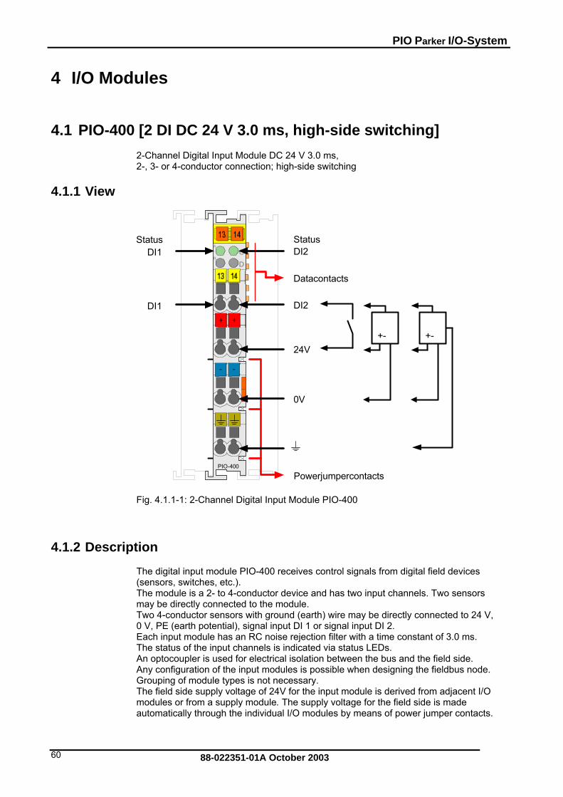
4.1 PIO-400 [2 DI DC 24 V 3.0 ms, high-side switching] 2 nput Module DC 24 V2 connection; high-s
4.1.1 View
-Channel Digital I 3.0 ms, -, 3- or 4-conductor ide switching
CD
B
A
+- +-
D
P umpercontacts
D ts
DSt
24
0V
S
400
4.1.2 Description
The digital inpu r nals from digital field devices (sensors, switches, etc.). The module is a 2- to 4-conductor device and has two input channels. Two sensors may be directly connected to the module.
wo 4-conductor sensors with ground (earth) wire may be directly connected to 24 V, 0 V, PE (earth potential), signal input DI 1 or signal input DI 2. Each input module has an RC noise rejection filter with a time constant of 3.0 ms. The status of the input channels is indicated via status LEDs. An optocoupler is used for electrical isolation between the bus and the field side. Any configuration of the input modules is possible when designing the fieldbus node. Grouping of module types is not necessary. The field side supply voltage of 24V for the input module is derived from adjacent I/O modules or from a supply module. The supply voltage for the field side is made automatically through the individual I/O modules by means of power jumper contacts.
I2
owerj
atacontac
I2atus
V
DI1tatus
DI1
PIO-
Fig. 4.1.1-1: 2-Channel Digital Input Module PIO-400
t module PIO-400 eceives control sig
T
88-022351-01A October 2003 60

EMN
The digital input module can be used with all couplers/controllers of the PASYSTEM PIO.
RKER-I/O-
4.1.3 Display
LED
Elements
Channel Designation State Function
off Input DI 1: Signal voltage (0)A green 1 Status
DI 1 on Input DI 1: Signal voltage (1)
off Input DI 2: Signal voltage (0)CD
B
A
CA
Fig. 4.1.3-1: Display Elements
C green 2 Status
DI 2 on Input DI 2: Signal voltage (1)
4.1.4 Schematic Diagram
1
2
3 7
4
5
6
8
2
4
6
8
3 7
10nF
DI1 DI2
24V
DI
0V10nF
DI
270pF
24V
0V
PIO-400
10nF
Fig. 4.1.4-1: 2-Channel Digital Input Module PIO-400
88-022351-01A October 2003 61

PIO Parker I/O-System
4.1.5 Technical Data
Module Spec aific D ta
Number of inputs 2
Current consumption (internal) A 3.7 m
Nominal volt 4 V (-1 /age DC 2 5 % +20%)
Signal voltag 3 V to e (0) DC - +5 V
Signal voltage (1) 5 V to DC 1 30 V
Input filter s 3.0 m
Current supp A ly typ. 4.5 m
I olation Veff (Fie ys 500 ld/S stem)
Internal bit width 2 Bit
Weight ca. 50 g
Approvals
UL E198563, UL508
KEMA 01ATEX1024 X II 3 G EEx nA II T4
GL (Germanischer Lloyd) 40 197-01 HH Cat. A, B, C, D
LR (Lloyd's Register) 02/20026 Env. 1, 2, 3, 4
DNV (Det Norske Veritas) A-8471 Cl. B
RINA (Registro Italiano Navale) MAC30402CS1
ABS (American Bureau of Shipping) 03-HG374860-PDA
Conformity marking CE
4.1.6 Process Image
Input bit B1 B0
Meaning Signal status Signal status DI 2 – Channel 2 DI 1 – Channel 1
88-022351-01A October 2003 62
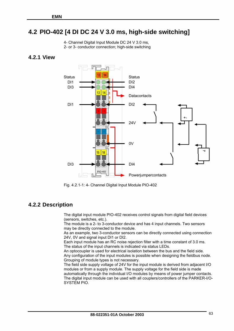
EMN
4.2 PIO-402 [4 DI DC 24 V 3.0 ms, high-side switching] 4- Channel Digital Input Module DC 24 V 3.0 ms, 2- or 3- conductor connection; high-side switching
4.2.1 View
CD
B
A
+-
DI2
Pow percontacts
Data
DI4DI2Sta
24V
0V
DI4
S
DI3
Fig. 4.2.1-1: 4- Channel Digital Input Module PIO-402
4.2.2 Description
nput module PIO-402 receives control signals from digital field devices (sensors, switches, etc.).
dule is a 2 3-conductor d direc to thxam c e
4V, 0V anach input module has an RC noise rejection filter with a time constant of 3.0 ms.
The status of the input channels is indicated via status LEDs. An optocoupler is used for electrical isolation between the bus and the field side.
ny configuration of the input modules is possible when designing the fieldbus node. Grouping of module types is not necessary. The field side supply voltage of 24V for the input module is derived from adjacent I/O modules or from a supply module. The supply voltage for the field side is made automatically through the individual I/O modules by means of power jumper contacts. The digital input module can be used with all couplers/controllers of the PARKER-I/O-SYSTEM PIO.
erjum
contacts
tus
DI3DI1
tatus
DI1
PIO-402
The digital i
The mo - to evice and has 4 input channels. Two sensors may beAs an e
tly connected ple, two 3-condu
d signal input DI1
e module. tor sensors can b
or DI2. directly connected using connection
2E
A
88-022351-01A October 2003 63

PIO Parker I/O-System
4.2.3 Display Elements
LED Channel Designation State Function
off Input DI 1: Signal voltage (0)A green
1 Status DI 1 on Input DI 1: Signal voltage (1)
off Input DI 2: Signal voltage (0)C green
2 Status DI 2 Input DI 2: Signal voltage (1)
DB
A
DC
BA C
D
on
off Input DI 3: Signal voltage (0)B green
3 Status DI 3 on Input DI 3: Signal voltage (1)
B
A
Fig. 4.2.3-1:
ts off Input DI 4: Signal voltage (0)Display Elemen
D green
4 Status DI 4
on Input DI 4: Signal voltage (1)
4.2.4 Schematic Diagram
1 5DI1 DI2 DI
2 6
3
4
7
8
10nF
0V0V
10nF
DI
DI DI4
PIO-402
270pF
24V24V
3
Fig. 4.2.4-1: 4-Channel Digital Input Module PIO-402
88-022351-01A October 2003 64

EMN
4.2.5 Technical a Dat
Module Specific Data
Number of inputs 4
Current consumption (internal) 7.5 mA
Nominal voltage DC 24 V (-15 % / +20 %)
Signal voltage (0) DC -3 V to +5 V
Signal voltage (1) DC 15 V to 30 V
Input filter 3.0 ms
Current supply typ. 4.5 mA
Isolation 500 Veff. (Field/System)
Internal bit width 4 Bit
Weight ca. 50 g
Approvals
UL E198563, UL508
KEMA 01ATEX1024 X II 3 G EEx nA II T4
GL (Germanischer Lloyd) 40 197-01 HH Cat. A, B, C, D
LR (Lloyd's Register) 02/20026 Env. 1, 2, 3, 4
DNV (Det Norske Veritas) A-8471 Cl. B
RINA (Registro Italiano Navale) MAC30402CS1
ABS (American Bureau of Shipping) 03-HG374860-PDA
Conformity marking CE
4.2.6 Process Image
Input bit B3 B2 B1 B0
Meaning I 4 – Channel 4
Signal status DI 3 – Channel 3 DI 2 – Channel 2
Signal status DI 1 – Channel 1
Signal status D
Signal status
88-022351-01A October 2003 65

PIO Parker I/O-System
4.3 PIO-430 [8 DI DC 24 V 3.0 ms, high-side switching] igital Input Module DC 24 V 3.0 ms,
1-conductor connection; high-side switching
4.3.1 V
8-Channel D
iew
StatusDI1…D8
DI1 DI2
DI3
DI5
DI4
DI6
Datacontacts
1: 8-Channel Digital Input Module PIO-430
4.3.2 Descrip
t DI 1, ... DI 8.
re isolated.
ical isolation between the bus and the field side. .
DI7 DI8
PowerjumpercontactsPIO-430
Fig. 4.3.1-
tion
The digital input module PIO-430 receives control signals from digital field devices (sensors, switches, etc.). The module is a 1-conductor device and has eight input channels. Eight 1-conductor sensors may be directly connected to signal inpuEach input module has an RC noise rejection filter with a time constant of 3.0 ms. All inputs aThe status of the input channels is indicated via status LEDs. An optocoupler is used for electrAny configuration of the input modules is possible when designing the fieldbus nodeGrouping of module types is not necessary.
The module posfield side to the following modules.
Note sesses power jumper contacts to pass through supply voltage for the
T field side s v 4 from adjacent I/O modules or from a supply module. The supply voltage fau matically ugh the individual s by me .
igital inp ule c be usedIO
he upply oltage of 2 V for the input module is derivedor the field side is made ans of power jumper contactsto thro
ut mod.
I/O module with all couplers/controllers of the PARKER-I/O-The d
SYSTEM Pan
88-022351-01A October 2003 66

EMN
4.3.3 Display Elements
LED Channel Designation State Function
ltage (0)off Input DI 1: Signal vogreen 1
Status
on l voltage (1)DI 1 Input DI 1: Signa
off Input DI 2: Signal voltage (0)green 2
Status DI 2 on oltage (1)Input DI 2: Signal v
off )Input DI 3: Signal voltage (0green 3
Status DI 3 l voltage (1)
DI2DI4DI6DI8
DI1DI3DI5DI7
on Input DI 3: Signa
off 0)Input DI 4: Signal voltage (green 4
Status DI 4
(1)on Input DI 4: Signal voltage
off )Input DI 5: Signal voltage (0green 5
Status DI 5 ltage (1)on Input DI 5: Signal vo
off Signal voltage (0)Input DI 6:green 6
Status DI 6 on Input DI 6: Signal voltage (1)
aus oltage (0)Input DI 7: Signal v
Fig. 4.3.3-1: Display Elements
green 7 Status DI 7 on Input DI 7: Signal voltage (1)
off Input DI 8: Signal voltage (0) green 8
Status DI 8 on Input DI 8: Signal voltage (1)
4.3.4 Schematic Diagram
1
2
3
4 8
5
6
7
DI1
DI3
DI5
24V
0V
DI2
DI4
DI6
DI8
DI
24V
0V
10nF
10nF
DI
0
Fig. 4.3.4-1: 8-Channel Digital Input Module PIO-430
DI7PIO-43
88-022351-01A October 2003 67

PIO Parker I/O-System
4.3.5 Technical Data
Module Specific Data
Number of inputs 8
Current consumption (internal) 17 mA
Signal voltage (0) DC -3 V to +5 V
Signal voltage (1) DC 15 V to 30 V
Input filter 3.0 ms
Current supply typ. 2.8 mA
Isolation 500 Veff (Field/System)
Internal bit width 8 Bit
Weight ca. 50 g
Approvals
UL E198563, UL508
DEMKO 02 AII 3 G
TEX 132273 X D EEx nA II T4
Conformity marking CE
4.3.6 Process Image
Input bit B7 B6 B5 B4 B3 B2 B1 B0
Meaning
C Channel 6
Sigstatus
Channel 5 Channel 4
Signal status
I 3 – Channel 3
Signal status DI 2 –
Channel 2
Signal status DI 1 –
Channel 1
Signal status
Signal status
Signal status
DI 8 – DI 7 – DI 6 – DIhannel 8 Channel 7
nal Signal status
5 – DI 4 – D
88-022351-01A October 2003 68

EMN
4.4 IOP -468 C 0-10 V, Single-Ended]
4.4.1 View
[4 AI D4-Channel Analog Input Module (0-10V, Single-Ended)
CB
A
D
PIO-468
FunctionAI2FunctionAI1FunctionAI3
AI2
AI4
cts
Common(ground)
Common(ground)
Shield(screen)
Shield(screen)
Dataconta
FunctionAI4
AI1
AI3
Fig. 4.4.1-1: 4-Channel Analog Input Module PIO-468
4.4.2 Description
The analog input module receives signals with the standardized values of 0-10 V. The module has four input channels. As an example, the fieldside signals may be received via the connections AI 1 and Common (ground) or AI 2 and Common (ground). The connection of more sensors to signal inputs AI 3 and AI 4 requires a suitable measure for the Common (ground) and the Shield (screen) connection, if need be. The input channels of a module have a common ground and a shield (screen) connection (S). The Shield (sreen) is directly connected to the DIN rail. A capacitive connection is made automatically when snapped onto the DIN rail. The input signal of each channel is electrically isolated and will be transmitted with a resolution of 12 bits. The operational readiness and the trouble-free internal data bus communication of the channels are indicated via a green function LED. Any configuration of the input modules is possible when designing the fieldbus node. Grouping of module types is not necessary The voltage supply is done via system voltage.
Attention This module has no power contacts. For field supply to downstream I/O modules, a supply module will be needed.
The analog input module can be used with all couplers/controllers of the PARKER-I/O-SYSTEM PIO.
88-022351-01A October 2003 69

PIO Parker I/O-System
4.4.3 Display Elements
LED Channel Designation State Function
off
No operational readiness or the internal data bus communication is interrupted A
green 1 Function AI 1
on Operational readiness and trouble-free internal data bus communication
off
No operational readiness or the internal data bus communication is interrupted C
green 2 Function AI 2
on Operational readiness and trouble-free internal data bus communication
off
No operational readiness or the internal data bus communication is interrupted B
green 3 Function AI 3
on Operational readiness and trouble-free internal data bus communication
off
No operational readiness or the internal data bus communication is interrupted
DB
A
DC
BA C
DB
A
Fig. 4.4.3-1: Display Elements
D green 4 Function
AI 4
on Operational readiness and trouble-free internal data bus communication
4.4.4 Schema
(groun
Shi(scre
A
A
10nF
DLogic
Function
Shield
tic Diagram
I1 AI2 Al A
Commond)
Common(ground)
elden) (screen)
I3 AI4
270pF
1 5
2 6
3 7
4
PIO-468
8
Fig. 4.4.4-1: 4-Channel Analog Input Module PIO-468
88-022351-01A October 2003 70

EMN
4.4.5 Technical Data
M dule Spec ao ific D ta
Number of inputs 4
Voltage supply stem avia sy volt ge DC /DC
Current consumption typ. (internal) A 60 m
Input voltage max. 35 V
Signal voltage 0 V... 10 V
Internal resistance typ. kΩ 133
Resolution it 12 B
Conversion time typ. 4 ms
Measuring error 25 °C <± 0,2 % of the full scale value
Temperature coefficient 1 % /K of<± 0,0 the full scale value
Isolation 500 Veff (system/supply)
Bit width 4 x 16 bits data 4 x 8 bits c oontr l / status(option)
Weight 5 g ca. 5
Approvals
UL E198563, UL508
KEMA 01ATEX1024 X II 3 G EEx nA II T4
GL (Germanischer Lloyd) 40 197-01 HH Cat. A, B, C, D
LR (Lloyd's Register) 02/20026 Env. 1, 2, 3, 4
DNV (Det Norske Veritas) A-8471 Cl. B
RINA (Registro Italiano Navale) MAC30402CS1
ABS (American Bureau of Shipping) 03-HG374860-PDA
Conformity marking CE
4.4.6 Process Image
The analog input module PIO-468 transmit 16-bit measured values and 8 status bits per channel. The digitalized measured value is transmitted in a data word (16 bits) as input byte 0 (low) and input byte 1 (high) into the process image of the coupler / controller. This value is represented with a 12 bit resolution on bit B3 ... B14. From the manufacturing number |32|02|XX|XX| onwards, the status information included in the three least significant bits (B0 ... B2) can be parsed in the event of an error. Bit B0 = 1 is set when the range of measurement is overranged. For modules having a previous manufacturing number, the last 3 bits are not parsed. The manufacturing number is part of the lateral marking on the module enclosure. Some fieldbus systems can process input channel status information by means of a status byte.
88-022351-01A October 2003 71

PIO Parker I/O-System
However, thaccessing o
e coupler / controller process operation is optional, which means that r parsing the status information depends on the fieldbus system.
ATh the process data s image depends on the fieldbus coupler/-controlleas of the r m the section "Fieldbus specific design of the process data" included in the description of the process image of the corresponding coupler/ controller.
ttention
e representation of of some fieldbus modules in the procesr used. Please take this information
espective control/status bytes fro well as the particular design
4.4.7 Standard
For the standard module PIO-468, the input voltage ranging from < 0 V to > 10 V is scaled on the numerical values ranging from 0x0000 to 0x7FF9.
Format
Process values of module PIO-468 numerical value Input current
binary status-
byte 0 - 10 V value *) X F Ü
hex. dec. hex.
0 0000 0000 0000 0 00 00 0 00 0005 0100 0000 0000 0 000 40 00 16384 00
10 0111 1111 1111 1 7F F8 32760 00 000 > 10 0111 1111 1111 1 7F F9 32761 42 001
*) status bits: X = not used, F = short-circuit, Ü = oversize
88-022351-01A October 2003 72

EMN
4.5 PIO-480 [2 AI 0-20 mA Differential Measurement Input]
t input
4.5.1 View
2-Channel Analog Input Module 0-20 mA, differential measuremen
CD
B
A
+AI2+AI1
Datacontacts
-AI2-AI1
Shield(screen)
Fig. 4.5.1-1: 2-Channel Analog Input Module 0-20 mA
4.5.2 Description
The odule recei f valu -20 The module has two differential input channels and can receive differential signals via the connections +AI 1 and - AIThe shi en) is d D c e tionmade automatically when snapped onto the DIN raThe inp l of ea is n tr ted w a resolution of 13 bits. The operational readiness and trouble-free internal data bus communication of the channe dicate e r w mea g range is ted viaAny con tion of t b d th bus . Groupin odule tyThe voltage supply is done via system voltage.
FunctionAI2FunctionAI1ErrorAI2ErrorAI1
Shield(screen)
PIO-480
analog input m ves differential signals o es 0 mA.
AI 1 or +AI 2 and - 2. eld (sre irectly connected to the IN rail. A
il. apacitiv connec is
ut signa ch channel is electrically olated a d will be ansmit ith
ls are in d via a Function LED. Ov rrange o underflo of the surin indica an Error LED. figura he input modules is possi le when esigning e field nodeg of m pes is not necessary.
AttentioThis mo as no p u own eam dule upply module will be needed.
n dule h ower contacts. For field s pply to d str I/O mo s, a
sThe analog input module can be used with all couplers/controllers of the PARKER-O-SYSTEM PIO. I/
88-022351-01A October 2003 73

PIO Parker I/O-System
4.5.3 Display Elements
LED Channel Designation State Function
off No operational readiness or the internal data bus communication is interrupted A
green Function
AI 1 on
Operational readiness and trouble-free internal data bus communication
off Normal operation B red
1
Error AI 1 on Overrange/underflow of the
range
C
admissible measuring
off No operational readiness or the internal data bus communication is interrupted C
green Function
AI 2 Operational readiness and
communication on trouble-free internal data bus
DB
AA C
B D Fig. 4.5.Display
3-1: Elements
2
off Normal operation
D red
Error AI 2 on Overrange/underflow of the
admissible measuring range tic Diagram 4.5.4 Schema
+AI1
Shield(screen)
-A
270pF
+AI2
-AI2-AI1
+Al
l
270pFA
DLogic
FunctionError
Shield(screen)
1
3
4
5
6
7
8
2
PIO-480
Fig. 4.5.4-1: 2-Channel Analog Input Module 0-20 mA
88-022351-01A October 2003 74

EMN
4.5.5 Technical Data
Module Specific Data
Number of outputs 2, electrically isolated from each other
Measured-value acquisition time synchronous (both inputs)
Voltage supply via system voltage DC /DC
Current consumption (internal) ≤ 100 mA
Signal current 0 ... 20 mA
Internal resistance < 270 Ω at 20 mA
Overrange/ measuring range underflow
status byte and LED
Input filter low pass first order, fG = 5 kHz
Resolution of the A/D converter 14 Bit
Monotonicity without missing codes
yes
Resolution of the measured value 13 Bit
Value of a LSB (Bit 2) 2.4 µA (Least Significant Bit)
Measuring error 25 °C ≤ ±0.05% of the full scale value
Temperature coefficient < ±0.01%/K of the full scale value
Measuring error ≤ 0.4 % over whole temperature range ≤ 0.1 % of upper range value (non-linearity)
Crosstalk attenuation ≥ 80 db
Sampling time of repetition 1 ms
Sampling delay (module) 1 ms
Sampling delay (channel/channel) ≤ 1 µs
Sampling duration ≤ 5 µs
Method of conversion SAR (Successive Approximation Register)
Operating mode continuously sampling (preset)
Protection non-linear limiting
Admissible continuous overload 30 V
Voltage resistance DC 500V channel/channel or channel/system
Bit width 2 x 16 bits data 2 x 8 Bit bits control/status (option)
Weight ca. 55 g
Approvals
UL E198563, UL508
DEMKO 02 ATEX 132273 X II 3 GD EEx nA II T4
Conformity marking CE
88-022351-01A October 2003 75

PIO Parker I/O-System
4.5.6 Process Image
The analog input module PIO-480 transmits 16-bit measured values and 8 optional s
T s transm data word (16 bits) as input byte 0 (low) and input byte 1 (high) into the process image of the coupler / controller. T it reT ficant bit15 (MSB) is alwayThe states of the first two least significant ined in the range b A. Therefore, they a ented with a ‘X‘ in the table. The hexadecimal and decimal measured values are listed in the table provided that t e '0'. If the s '1' is taken into consideration for both bits, the decimal measured value will be higher by the value 3 as it is indicated in the table.
S can process inpu formation by means of a status byte. However, processing via the coupler / controller is optional, which means that a ati ystem.
tatus bits per channel.
he digitalized measured value i itted in a
his value is represented with a 13 b solution on bit B2 ... B14. he most signi s '0'.
bits B0 and B1 are not defetween 0 and 20 m re repres
he first two bits have the stat tate
ome fieldbus systems t channel status in
ccessing or parsing the status inform on depends on the fieldbus s
AThe representation of the process data of some I/O modules in the process image depends on the fieldbus coupler/-controller used.as the particular design of the respective control/status bytes from the section "Fieldbus Specific Design of the Process Data" included in the description concerning the process image of the corresponding coupler/controller.
ttention
Please take this information as well
4.5.7 Standard
For the standard module PIO-480, the in 0 mA to > 20 mA is scaled on the numerical values ranging from 0x0000 to 0x7FFF.
Format
put current ranging from <
Process values of module PIO-480
Input current
numerical value status-
byte LED error
0 - 20 mA binary hex. dec. hex. AI 1, 2 > 21 '0111.1111.1111.11XX' 0x7FF
C 32764 0x42 on
> 20 '0111.1111.1111.11XX' 0x7FFC
32764 0x00 off
20,00 '0111.1111.1111.11XX' 0x7FFC
32764 0x00 off
17,50 '0111 0.0000.00X 0x7000 28672 0x00 off .000 X' 15,00 '0110.0000.0000.00XX' 0x6000 24576 0x00 off 12,50 0 20480 0x00 off '0101.0000.0000.00XX' 0x50010,00 '0100.0000.0000.00XX' 000 16384 0x00 off 0x47,50 '0011.0000.0000.00XX' 0x3000 12288 0x00 off 5,00 '0010.0000.0000.00XX' 0x2000 8192 0x00 off 2,50 '0001.0000.0000.00XX' 0x1000 4096 0x00 off 0,00 '0000.0000.0000.00XX' 0x0000 0 0x00 off < 0 '0000.0000.0000.00XX' 0x0000 0 0x00 off < -1 '0000.0000.0000.00XX' 0x0000 0 0x41 on
88-022351-01A October 2003 76
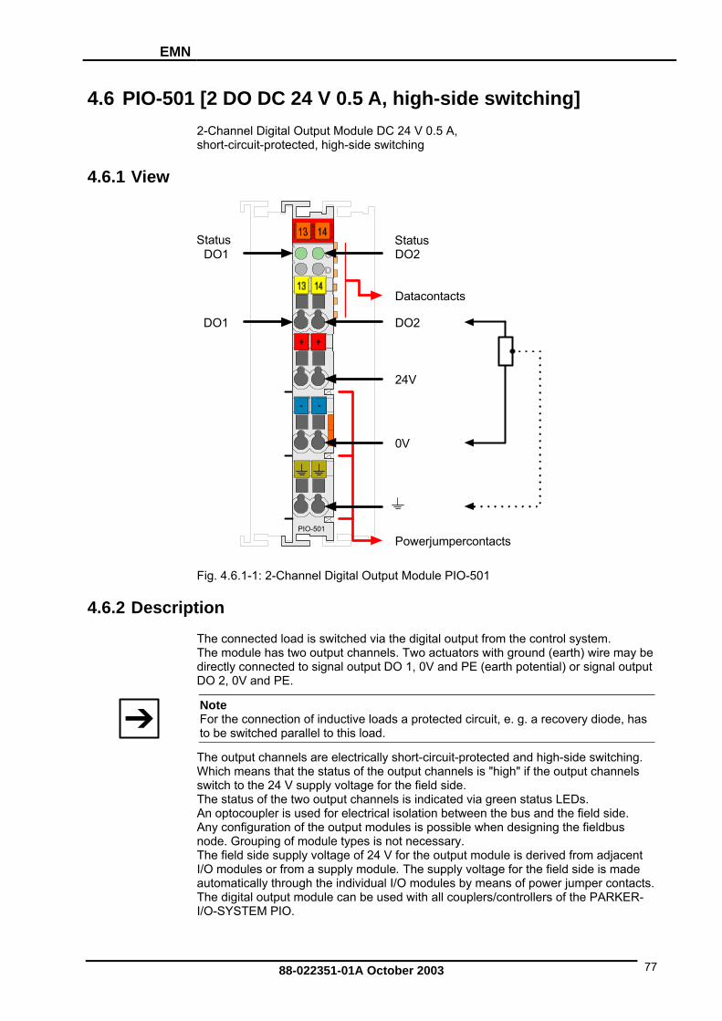
EMN
4.6 PIO-501 [2 DO DC 24 V 0.5 A, high-side switching] 2-Channel Digital Output Module DC 24 V 0.5 A, short-circuit-protected, high-side switching
4.6.1 View
CD
B
A
DO2DO1StatusStatus
Datacontacts
DO2DO1
PIO-501
Powerjumpercontacts
24V
4.6.2 Descrip
gital output from the control system. two output channels. Two actuators with ground (earth) wire may be
directly connected to signal output DO 1, 0V and PE (earth potential) or signal output D 2, 0V and
0V
Fig. 4.6.1-1: 2-Channel Digital Output Module PIO-501
tion
The connected load is switched via the diThe module has
O PE.
Note For the connection of inductive loads a protected circuit, e. g. a recovery diode, has to be switched parallel to this load.
The outputWhich mea
ch are e trically s uit-pr te . ns status of the ou annels hi nels
switch to the 24 V supply voltage for the field side. The status of outp channels ated v reAn optocoupler is used for electrical is betwe h e. Any configuration of the output modules is possible when designing the fieldbus node. Grouping of module types is not necessary. T field side voltage of 24 V f utput u cent I/O modules or from a supply module. The supply voltage for the field side is made utomatically through the individual I/O modules by means of power jumper contacts. he digital output module can be used with all couplers/controllers of the PARKER-
I/O-SYSTEM PIO.
annels that the
lec hort-circtput ch
otec d and high-side switching is " gh" if the output chan
the two ut is indicolation
ia g en status LEDs. en t e bus and the field sid
he supply or the o mod le is derived from adja
aT
88-022351-01A October 2003 77

PIO Parker I/O-System
4.6.3 Display Elements
LED Channel Designation State Function
off Output DO 1: not active A green 1 Status
DO 1 on Output DO 1: active
off Output DO 2: not active CD
B
A
CA
Fig. 4.6.3-1: Display Elements
C green 2 Status
DO 2 on Output DO 2: active
4.6.4 Schematic Diagram
1
2 6
3 7
4 8
5
PIO-501
DO1 DO2 DO
0V
C
10nF
DO10nF
Fig. 4.6.4-1: 2-Channel Digital Output Module PIO-501
24V24V
0V
88-022351-01A October 2003 78

EMN
4.6.5 Technical Data
Module Specific Data
Number of outputs 2
Current consumption (internal)max. 3.5 mA
Voltage via power jumper contacts 24 V (-15 % / +20%) DC
Type of load resistive, inductive, lamps
Switching rate max. 5 kHz
Reverse voltage protection no
Output current 0.5 A
Absorbable energy W(unique switching off) max.
max. 0.5 J Lmax. = 2 W /I²
Isolation 500 V (system/field)
Current consumption typ.(field side) 15 mA (per module) + load
Internal bit width 2 Bit out
Weight ca. 50 g Approvals UL E198563, UL508
KEMA 01ATEX1024 X II 3 G EEx nA II T4
GL (Germanischer Lloyd) 40 197-01 HH Cat. A, B, C, D (EMC1)
LR (Lloyd's Register) 02/20026 Env. 1, 2, 3, 4
DNV (Det Norske Veritas) A-8471 Cl. B
RINA (Registro Italiano Navale) MAC30402CS1
ABS (American Bureau of Shipping) 03-HG374860-PDA
Conformity marking CE
4.6.6 Process Image
Output bit B1 B0
Meaning controls DO 2 controls DO 1 Channel 2 Channel 1
88-022351-01A October 2003 79

PIO Parker I/O-System
4.7 PIO-504 [4 DO DC 24 V 0.5 A, high-side switching] 4-Channel Digital Output Module DC 24 V 0.5 A, short-circuit-protected, high-side switching
4.7.1 View
CD
B
A
PIO-504
D
Powerjumpercontacts
D tacts
DS
2
0V
DO4
DO1Status
DO4DO3
DO3
Fig. 4.7.1-1: 4-Channel Digital Output Module PIO-504
4.7.2 Description
The connected load is switched via the digital output from the control system. The module has four output channels. Two actuators may be directly connected to the module. As an example, two 2-conductor actuators may be directly connected using connection 0 V and signal output DO 1 or 0 V and signal output DO 2.
O2
atacon
O2tatus
4V
DO1
Note For the connection of inductive loads a protected circuit, e. g. a recovery diode, has to be switched parallel to this load.
The output channels are electrically short-circuit-protected and high-side switching. Which means that the status of the output channels is "high" if the output channels switch to the 24 V supply voltage for the field side. The supply voltage for the field side is derived from an adjacent supply module by means of power jumper contacts.
een status LEDs. An optocoupler is used for electrical isolation between the bus and the field side.
ny configuration of the output modules is possible when designing the fieldbus node. Grouping of module types is not necessary.
The status of the four output channels is indicated via gr
A
88-022351-01A October 2003 80
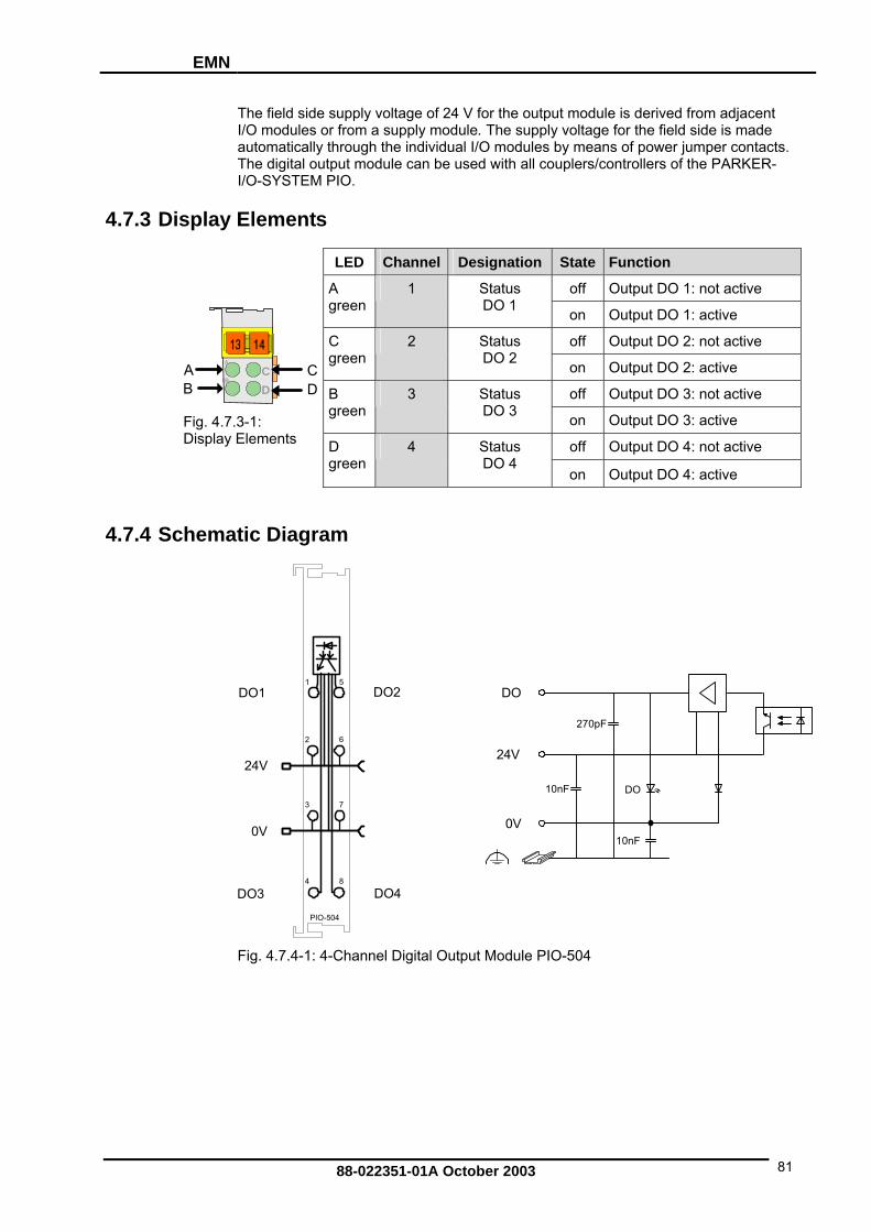
EMN
The field sidI/O modules
e supply voltage of 24 V for the output module is derived from adjacent or from a supply module. The supply voltage for the field side is made
automatically through the individual I/O modules by means of power jumper contacts. The digital output module can be used with all couplers/controllers of the PARKER-I
4.7.3 Display E
LED
/O-SYSTEM PIO.
lements
Channel Designation State Function
off Output DO 1: not active A green
1 Status DO 1 on Output DO 1: active
off Output DO 2: not active C green
2 Status DO 2 on Output DO 2: active
off Output DO 3: not active B green
3 Status DO 3 on Output DO 3: active
DB
A
DC
BA C
DB
A
Fig. 4.7.3Display E O 4: not active
-1: lements off Output D
greenD
4 Status
DO 4 on Output DO 4: active
4.7.4 Schematic
DO3 DO4
DO
24
0V
DO
0V
F
10nF
DO10nF
Diagram
DO1 2
V
270p
24V
1
3
5
7
2 6
4 8
PIO-504
Fig. 4.7.4-1: 4-Channel Digital Output Module PIO-504
88-022351-01A October 2003 81

PIO Parker I/O-System
4.7.5 Technical Data
Module Specific Data
Number of outputs 4
Current consumption (internal)max. 7 mA
Voltage via power jumper contacts DC 24 V (-15 % / + 20 %)
Type of load resistive, inductive, lamps
Switching rate max. 1 kHz
Reverse voltage protection no
Output current 0.5 A short-circuit-protected
Absorbable energy Wmax. (unique switching off)
0.3 J L = 2 W /I² max. max.
Isolation 500 V (system/field)
Current consumption typ.(field side) 30 mA (per module) + load
Internal bit width 4 Bit out
Weight ca. 50 g
Approvals
UL E198563, 0UL5 8
KEMA X1024 X EEx nA II
01ATEII 3 G T4
GL (Germanischer Lloyd) 40 197-01 HH Cat. A, B, C, D (EMC1)
LR (Lloyd's Register) 02/20026 Env. 1, 2, 3, 4
DNV (Det No eritas 71 Cl. B
rske V ) A-84
RINA (Registro Italiano Navale) MAC30402CS1
ABS (American Bureau of Shipping) 03-HG374860-PDA
Conformity marking CE
4.7.6 Process Image
Output bit B3 B2 B1 B0
Meaning controls DO 4Channel 4
controls DO 3Channel 3
controls DO 2 Channel 2
controls DO 1Channel 1
88-022351-01A October 2003 82
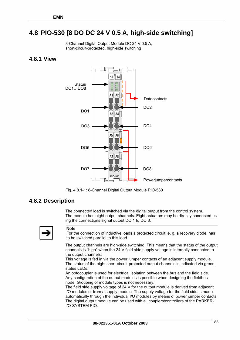
EMN
4.8 PIO-530 [8 DO DC 24 V 0.5 A, high-side switching] 8-Channel Digital Output Module DC 24 V 0.5 A, short-circuit-protected, high-side switching
4.8.1 View
PIO-530
StatusDO1…DO8
DO1
DO3
DO5
DO7
DO6
DO8
Datacontacts
Powerjumpercontacts
DO4
DO2
F annel Digital Output Mo
4.8.2 Description
The connected load is switched via the di put from the control system. The module has eight output channels. Eight ing the connections signal output DO 1 to DO 8.
ig. 4.8.1-1: 8-Ch dule PIO-530
gital outactuators may be directly connected us-
Note For the connection of inductive loads a p diode, has to be switched parallel to this load.
rotected circuit, e. g. a recovery
The output channels are high-side switching. This means that the status of the output c "high" when the 24 V field sid lly connected to the output channels. This voltage is fed in via the power jumper contacts of an adjacent supply module. The status of the eight short-circuit-protected output channels is indicated via green status LEDs. An optocoupler is used for electrical isolation between the bus and the field side. Any configuration of the output modules is possible when designing the fieldbus n Grouping of module types is not neThe field side supply voltage of 24 V for t is derived from adjacent I/O modules or from a supply module. The supply voltage for the field side is made automatically through the individual I/O m f power jumper contacts. T n be used w ontrollers of the PARKER-I/O-SYSTEM PIO.
hannels is e supply voltage is interna
ode. cessary. he output module
odules by means ohe digital output module ca ith all couplers/c
88-022351-01A October 2003 83

PIO Parker I/O-System
4.8.3 Display Elements
LED Channel Designation State Function
off Output DO 1: not active green 1
StaDO tput DO 1: active
tus 1 on Ou
off Output DO 2: not active green 2
StaDO on Output DO 2: active
tus 2
off Output DO 3: not active green 3
Status DO 3 on Output DO 3: active
off Output DO 4: not active green 4
Status DO 4
on Output DO 4: active
off Output DO 5: not active green 5
Status DO 5 on Output DO 5: active
off Output DO 6: not active green 6
Status DO 6 on Output DO 6: active
off Output DO 7: not active
DO8
DO1
DO5DO7
Fig. 4.8.3-1: Display Elements
green 7 Status DO 7 on Output DO 7: active
off Output DO 8: not active green 8
Status DO 8 on Output DO 8: active
4.8.4 Schematic Diagram
PIO-530
1
2
3
4
5
6
7
8
DO1
DO3
DO5
DO7
DO6
DO8
DO4
DO2
24 V
0 V
DO
24 V
0 V
270 pF
10 nF 10 nF DO
10 nF
Fig. 4.8.4-1: 8-Channel Digital Output Module PIO-530
88-022351-01A October 2003 84

EMN
4.8.5 Technical Data
Module Specific Data
Number of outputs 8
Current consumption (internal) 25 mA
Voltage via power jumper contacts DC 24 V (-15 % / +20%)
Type of load resistive, inductive, lamps
Switching rate max. 2 kHz
Reverse voltage protection yes
Output current 0.5 A short-circuit-protected
Absorbable energy W (unique switching
0.9 J max. off) Lmax. = 2 Wmax. /I²
I /field) solation 500 V (system
Current consumption typ.(f A (per m e) + ield side) 15 m odul load
Internal bit width t 8 Bit ou
Weigh t ca. 50 g
Approvals
UL E198563, UL508
DEMK X 13 EEx 4
O 02 ATE 2273 XII 3 GD nA II T
Conformity marking CE
4.8.6 Process Image
Output bit
B7 B6 B5 B4 B3 B2 B1 B0
Meaning controls DO 8 –
Channel 8
controls DO 7 –
Channel 7
contDO
Channel 6
rols 6 –
controls DO 5 –
Channel 5
controls DO 4 –
Channel 4
controls DO 3 –
Channel 3
controls DO 2 –
Channel 2
controls DO 1 –
Channel 1
88-022351-01A October 2003 85
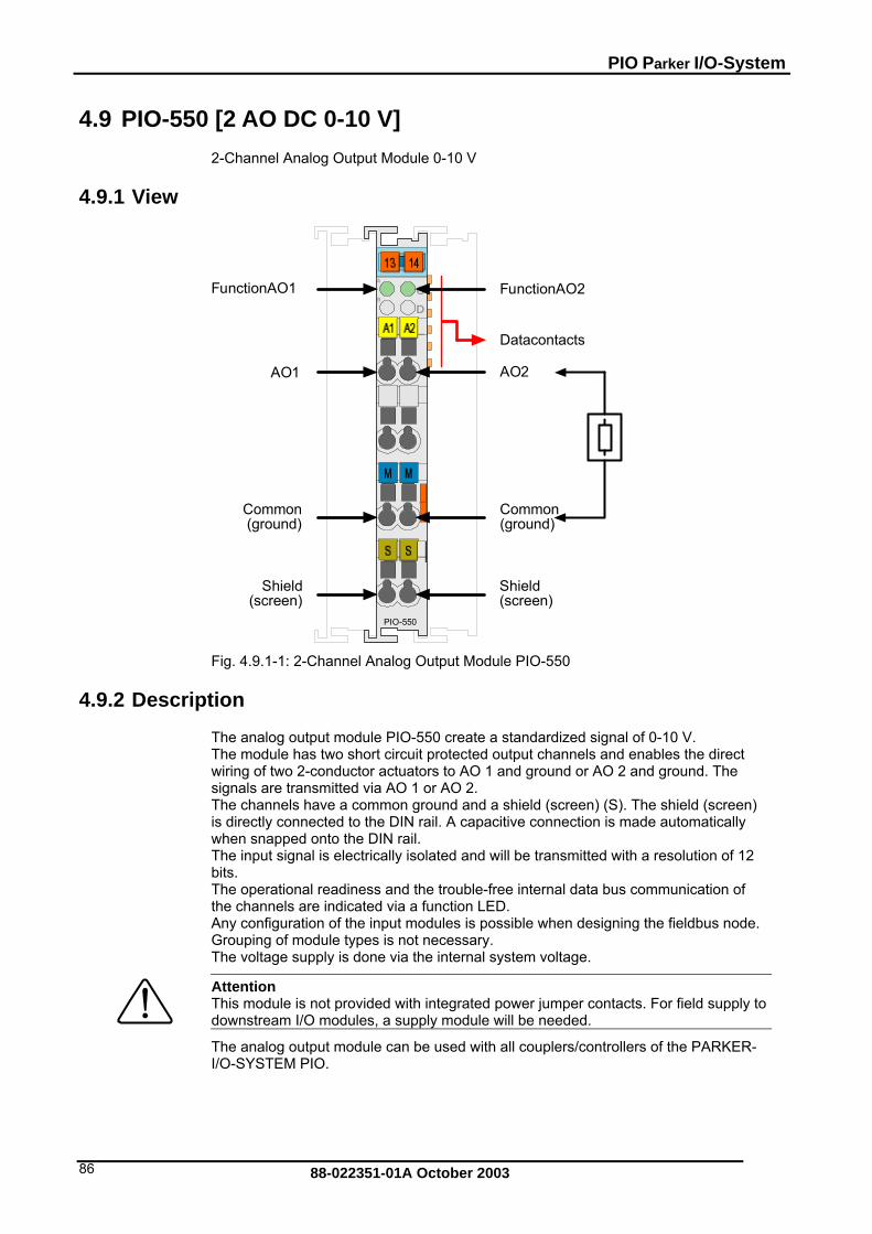
PIO Parker I/O-System
4.9 PIO-550
4.9.1 View
[2 AO DC 0-10 V] 2-Channel Analog Output Module 0-10 V
CD
B
A
PIO-550
AO2
FunctionAO2onAO1
Shield(screen)
Shield(screen)
ommonround)
Common(ground)
Functi
Datacontacts
AO1
C(g
Fig. 4.9.1-1: 2-Channel Analog Output Module PIO-550
4.9.2 Description
he analog output module PIO-550 create a standardized signal of 0-10 V. ted output channels and enables the direct
wiring of two 2-conductor actuators to AO 1 and ground or AO 2 and ground. The signals are transmitted via AO 1 or AO 2. The channels have a common ground and a shield (screen) (S). The shield (screen) is directly connected to the DIN rail. A capacitive connection is made automatically when snapped onto the DIN rail. The input signal is electrically isolated and will be transmitted with a resolution of 12 bits. The operational readiness and the trouble-free internal data bus communication of the channels are indicated via a function LED. Any configuration of the input modules is possible when designing the fieldbus node. Grouping of module types is not necessary. The voltage supply is done via the internal system voltage.
TThe module has two short circuit protec
Attention This module is not provided with integrated power jumper contacts. For field supply to downstream I/O modules, a supply module will be needed.
The analog output module can be used with all couplers/controllers of the PARKER-I/O-SYSTEM PIO.
88-022351-01A October 2003 86

EMN
4.9.3 Display Elements
LED Channel Designation State Function
off No operational readiness or the internal data bus communication is interrupted A
green 1 Function AO 1
on Operational readiness and trouble-free operational readiness
off No operational readiness or the internal data bus communication is interrupted
CD
B
A
CA
Fig. 4.9.3-1: Display Elements
C green 2 Function
AO 2 on
Operational readiness and trouble-free operational readiness
4.9.4 Schematic Diagram
AD
Logic
(s
C Co(g
Shield(screen)
AO1 AO2 AO
10nF
270pF
Function
Shieldcreen)
ommon(ground)
mmonround)
1 5
2
3 7
4
6
8
PIO-550
F alog Output
4.9.5 Technical Data
ig. 4.9.4-1: 2-Channel An Module PIO-550
Module Specific Data
Number of outputs 2
Voltage supply via system voltage DC/DC
Current consumption typ. (internal) 65 mA
Signal voltage 0 ... 10 V
Load impedance > 5 kΩ
88-022351-01A October 2003 87

PIO Parker I/O-System
Resolution 12 Bit
Conversion time . 2 typ ms
Measuring error 25°C % of the full scale value <± 0,1
Temperature coefficient <± 0,01 %/°K of the full scale value
Isolation 500 Veff (system/supply)
Bit width 2 x2 x 8 bits control/status(option)
16 bits data
Weight ca. 55 g
Approvals
UL E198563, UL508
KEMA 01ATEX1024 X II3G EEx nA II T4
GL (Germanischer Lloyd) 40 197-01 HH Cat. A,B,C,D (EMC1)
LR (Lloyd's Register) 02/20026 Env. 1, 2, 3, 4
DNV (Det Norske Veritas) A-8471 Cl. B
RINA (Registro Italiano Navale) MAC30402CS1
ABS (American Bureau of Shipping) 03-HG374860-PDA
Conformity marking CE
88-022351-01A October 2003 88
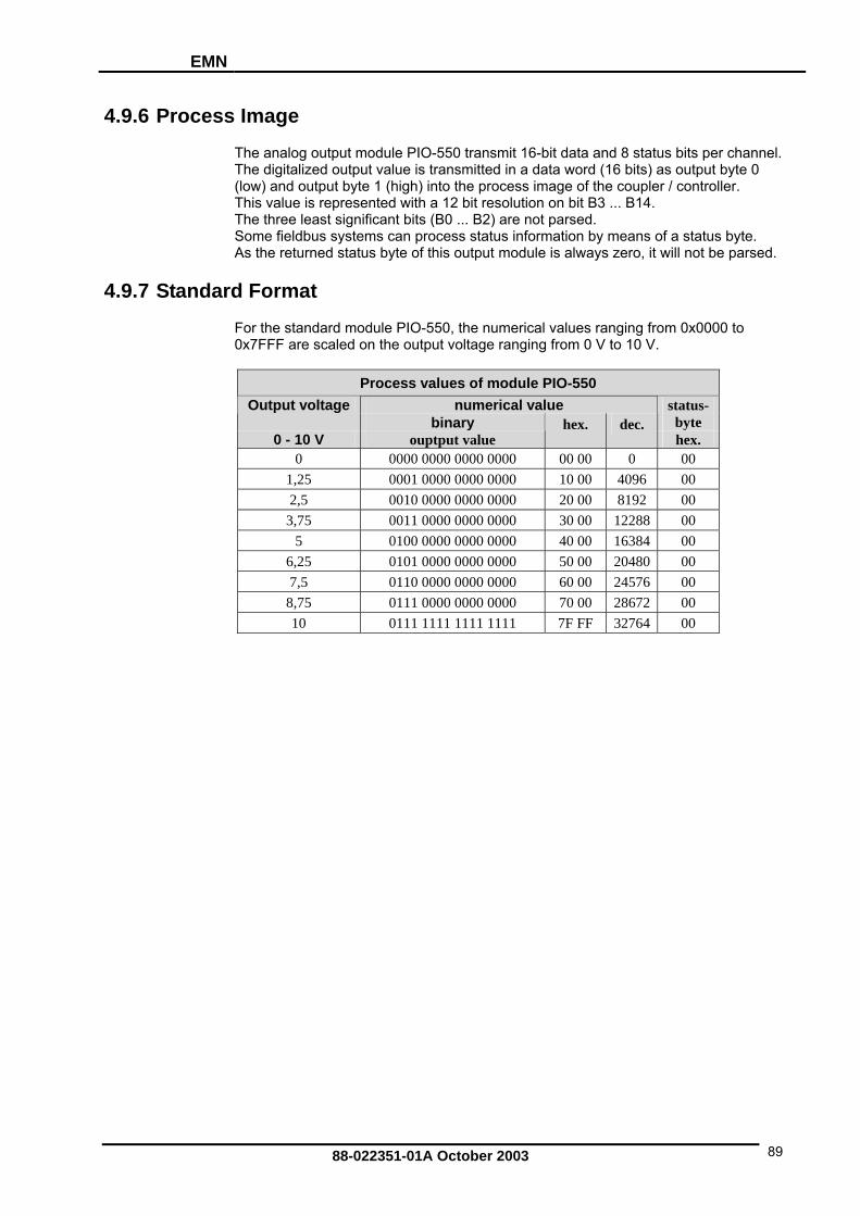
EMN
4.9.6 Process Image
The analog output module PIO-550 transmit 16-bit data and 8 status bits per channel. The digitalized output value is transmitted in a data word (16 bits) as output byte 0 (low) and output byte 1 (high) into the process image of the coupler / controller. This value is represented with a 12 bit resolution on bit B3 ... B14. The three least significant bits (B0 ... B2) are not parsed.
. ed status byte of this output module is always zero, it will not be parsed.
For the standard module PIO-550, the numerical values ranging from 0x0000 to
Some fieldbus systems can process status information by means of a status byteAs the return
4.9.7 Standard Format
0x7FFF are scaled on the output voltage ranging from 0 V to 10 V.
Process values of module PIO-550 numerical value Output voltage
binary status-
byte 0 - 10 V ouptput value
hex. dec. hex.
0 0000 0000 0000 0000 00 00 0 00 1,25 4096 0001 0000 0000 0000 10 00 00 2,5 0010 0000 0000 0000 20 00 8192 00
3,75 0011 0000 0000 0000 30 00 12288 00 5 0100 0000 0000 0000 40 00 16384 00
6,25 0101 0000 0000 0000 50 00 20480 00 7,5 0110 0000 0000 0000 60 00 24576 00
8,75 0111 0000 0000 0000 70 00 28672 00 10 0111 1111 1111 1111 7F FF 32764 00
88-022351-01A October 2003 89

PIO Parker I/O-System
4.10 PIO-552 [2 AO 0-20 mA] 2-Channel Analog Output Module 0-20 mA.
4.10.1 View
CD
B
A
PIO-552
AO2
Datacontacts
Powerjumpercontacts
0V
FunctionAO1
AO1
Shield(screen)
Shield(screen)
FunctionAO2
24V
Fig. 4.10.1-1: 2-Channel Analog Output Module PIO-552
4.10.2 Description
The analog output module PIO-552 create a standardized signal of 0-20 mA. The module has two output channels and enables, for example, the direct wiring of two 2-conductor actuators to the connections AO 1 and 0V or AO 2 and 0V. The signals are transmitted via AO 1 or AO 2. The channels have a common ground and a shield (screen) (S). The shield (screen) is directly connected to the DIN rail. A capacitive connection is made automatically when snapped onto the DIN rail. The input signal is electrically isolated and will be transmitted with a resolution of 12 bits. The operational readiness and the trouble-free internal data bus communication of the channels are indicated via a green function LED. Any configuration of the input modules is possible when designing the fieldbus node. Grouping of module types is not necessary. The voltage supply is done via the field supply. The field side supply voltage of 24 V for the output module is derived from an adjacent I/O module or from a supply module. A capacitive connection of the supply potential to the adjacent I/O modules is made automatically via the internal power contacts when snapping the output modules.
88-022351-01A October 2003 90

EMN
Note Use an appropriate supply module (e.g. PIO-602) if an electrically isolated voltage supply is required!
The analog output module can be used with all couplers/controllers of the PARKER-M PIO.
4.10.3 Display Elements
LED
I/O-SYSTE
Channel Designation State Function
off
No operational readiness or the internal data bus communication is interrupted A
green 1 Function AO 1
on Operational readiness and trouble-free internal data bus communication
off
No operational readiness or the internal data bus communication is interrupted
CD
B
A
CA
Fig. 4.10.3-1: Display Elements
C green 2 Function
AO 2
on Operational readiness and trouble-free internal data bus communication
4.10.4 Schematic Diagram
(scre
A
2
270pF 10nF 10nF
Logic
Function
O1 AO2 AO AI
4V 24V
DU
Shielden)
Shield(screen)
0V10nF
0V
1 5
2 6
3 7
4 8
PIO-552
Fig. 4.10.4-1: 2-Channel Analog Output Module PIO-552
88-022351-01A October 2003 91

PIO Parker I/O-System
4.10.5 Technical Data
M dule Sp Do ecific ata
Number of outputs 2
Voltage supp via system voltage DC 24 V (-15% ... +20%) ly
Current consumption ty al) mAp. (intern 60
Signal voltage 0... 20 mA
Load impedance < 500 Ω
Linearity ± 2 LSB
Resolution 12 Bit
Conversion time typ. 2 ms
Measurung error 25°C <± 0,1 % of the full scale value
Temperature coefficient <± 0,01 %/°K of the full scale value
Isolation 500 Veff (system/supply)
Bit width 2 x 16 bits data 2 x 8 bits control/status(option)
Weight ca. 55 g
Approvals
UL E198563, UL508
KEMA 01ATEX1024 X II 3 G EEx nA II T4
GL (Germanischer Lloyd) 40 197-01 HH Cat. A, B, C, D (EMC1)
LR (Lloyd's Register) 02/20026 Env. 1, 2, 3, 4
DNV (Det Norske Veritas) A-8471 Cl. B
RINA (Registro Italiano Navale) MAC30402CS1
ABS (American Bureau of Shipping) 03-HG374860-PDA
Conformity marking CE
88-022351-01A October 2003 92

EMN
4.10.6 Process Image
The analog output module PIO-552 transmit 16-bit data and 8 status bits per channel. The digitalized output value is transmitted in a data word (16 bits) as output byte 0 (low) and output byte 1 (high) via the pr ge of the coupler / controller. T value is represented with a 12 bit resolution on bit B3 ... B14.The three least s eS he s information using by means of a status byte. A urned status byte of this outpu is always zero, it will not be parsed.
4.10.7 Standard
For the standard module PIO-552, the numerical values ranging from 0x0000 to 0x7FFF are scaled on the output current ranging from 0 mA to 20 mA.
ocess imahisignificant bits (B0 ... B2) are not parsome fieldbus systems can process t
d. statu
s the ret t module
Format
Process values of module PIO-552 numerical value Ouput current
binary status-
byte 0 - 20 mA output value
hex. dec. hex.
0 0000 0000 0000 00 00 0 00 0000 2,5 0001 0000 0000 10 00 4096 00 0000 5 0010 0000 0000 8192 00 0000 20 00
7,5 0011 0000 0000 2288 00 0000 30 00 110 0100 0000 0000 0000 40 00 16384 00
12,5 0101 0000 0000 0000 50 00 20480 00 15 0110 0000 0000 0000 60 00 24576 00
17,5 0111 0000 0000 0000 70 00 28672 00 20 0111 1111 1111 1111 7F FF 32764 00
88-022351-01A October 2003 93

PIO Parker I/O-System
4.11 PIO-600 [End Module] ule
4.11.1 Vie
End Mod
w
CA
DB
PIO-600
Fig. 4.11.1-1: End Module PIO-600
4.11.2 Description
fter the fieldbus node is assembled with the correct buscoupler and selected I/O modules , the end module PIO-600 is snapped onto the assembly. This module completes the internal data circuit and ensures correct data flow. The end module is a necessary component to all PARKER-I/O-SYSTEM PIO fieldbus nodes.
A
88-022351-01A October 2003 94

EMN
4.11.3 Technical Data
Module Specific Data
Weight ca. 35 g
Approvals
UL E198563, UL508
KEMA 01ATEX1024 X II 3 G EEx nA II T4
GL (Germanischer Lloyd) 40 197-01 HH Cat. A, B, C, D (EMC1)
LR (Lloyd's Register) 02/20026 Env. 1, 2, 3, 4
DNV (Det Norske Veritas) A-8471 Cl. B
RINA (Registro Italiano Navale) MAC30402CS1
ABS (American Bureau of Shipping) 03-HG374860-PDA
Conformity marking CE
88-022351-01A October 2003 95

PIO Parker I/O-System
4.12 PIO-602 [24 V DC Power Supply]
4.12.1 View
Supply Module DC 24 V, passive
CD
B
A
PIO-602
0V
Powerjumpercontacts
Status voltage supply-Powerjumpercontacts
Supply via power-jumper-contacts24V
Datacontacts
Fig. 4.12.1-1: Suppy Module PIO-602
4.12.2 Description
The supply module PIO-602 provides an electrically isolated DC 24 V fieldside power to the adjacent I/O modules. The module is fed in external via the 24 V, 0V and PE (earth potential) connections.
nt I/O modules is made automatically via the internal power contacts when snapping the I/O modules A capacitive connection of the potentials to the adjace
together.
Note Maximum current supply to all connected modules is 10 A. Should more current be needed, additional supply modules may be added in the assembly. Note Pay particular attention to the admissible voltage of each I/O module when using the supply modules.
The operating voltage of 24 V is indicated via a green status LED. b d ing th dbus Any configuration of the output modules is possi le when esign e fiel
node. Grouping of module types is not necessary. The supply module can be used with all couplers/controllers of the PARKER-I/O-SYSTEM PIO.
88-022351-01A October 2003 96

EMN
4.12.3 Dis
LED Designation State Function
play Elements
off No DC 24 V voltage supply via power jumper contacts.
CD
B
A
C C
Status voltage supply –Power
Fig. 4.12Display E
green jumper contacts
on DC 24 V voltage supply via power jumper contacts. .3-1:
lements
4.12.4 Schematic Diagram
Status
0V0V
24V24V
1
2
3
5
6
7
4 8
PIO-602
Fig. 4.12.4-1: Supply Module PIO-602
88-022351-01A October 2003 97

PIO Parker I/O-System
4.12.5 Technical Data
Module Specific Data
Voltage via power jumper contacts max
DC 24 V
Current via power jumper contacts max.
10 A
Weight ca. 45 g
Approvals
UL E198563, UL508
KEMA 01ATEX1024 X II 3 G EEx nA II T4
GL (Germanischer Lloyd) 1) 40 197-01 HH Cat. A, B, C, D
LR (Lloyd's Register) 1) 02/20026 Env. 1, 2, 3, 4
DNV (Det Norske Veritas) 1) A-8471 Cl. B
RINA (Registro Italiano Navale) 1) MAC30402CS1
ABS (American Bureau of Shipping) 1)
03-HG374860-PDA
Conformity marking CE 1) Note information on “Voltage Supply“!
88-022351-01A October 2003 98
EMN
5 CANopen 5.1 Descrip
is-he
data backup layer. The message structure is exactly described, how-s
eneral de-scriptive language for CAN networks and provides a large number of communication services.
e serial bus I/O-system CAN. yer by the DS 301 specifications of the
work
e
owed to send messages. Bus con-ty is d to a . This
ubscribers to send data.
his request is performed via the so-called remote frame.
ecification (DS 301) defines the technical and functional features distributed field automation devices.
tion CAN (Controller Area Network) was developed in the mid-eighties for data transmsion in automobiles. The CAN specification defines the Data Link Layer which is tphysical andever, nothing is said regarding the Application Layer. CAL, in the contrary, describethe Application Layer or the Meaning of the transmitted data. CAL is a g
CANopen is a networking concept based on thCANopen is defined as a uniform application laCIA (CAN in automation).
The network management provides a simplified start-up of the network. This netcan be extended by the user as desired.
CAN is a Multimaster bus I/O-system. In contrast to other fieldbus I/O-systems, thmodules connected to the bus are not addressed but the messages identified. Whenever the bus is free, the subscribers are allflicts are solved in that the messages are assigned a certain priority. This prioridefined by the COB ID (Communication Object Identifier) and is clearly assignecommunication object. The smaller the assigned identifier, the higher the priorityalso allows communication without the bus master group.
Each bus subscriber is solely decisive as to the point in time of data transmission.However, there is also a possibility to request other bus sT
The CANopen spused to network
i
Further information C embers in the Internet under:
AN in Automation (CiA) provides further documents for their m
can-cia.de
88-022351-01A October 2003 99

PIO Parker I/O-System
5.2 Network architecture
5.2.1 Transmission media
Type of cable
twisted in pairs) with a wave resistance of 108...132 Ohm is recommended. Twisted-Pair is low priced, convenient to use and permits simple bus type wiring.
• the maximum bus length and
• the required conductor cross section.
Maximum bus length
bus is mainly limited by the signal running time and must, therefore, Baud rate:
A bus medium forms the basis for the physical connection of CAN. With CAN, both the bus coupling and the bus medium are specified according to ISO 11898 (CAN High-Speed).
According to the cable specification, the Twisted-Pair medium (shielded cables
The CANopen fieldbus nodes are intended for wiring using shielded copper wire (3x0.25 mm²).
Two important points have to be taken into consideration when designing the electri-cal bus medium:
The length of thebe adapted to the
Baud rate Bus length 1 Mbit/s 30 m 800 kbit/s 50 m 500 kbit/s 100 m 250 kbit/s 250 m 125 kbit/s 500 m ≤ 50 kbit/s 1000 m
Table 5-1: Maximum bus length dependent on the set Baud rate
88-022351-01A October 2003 100
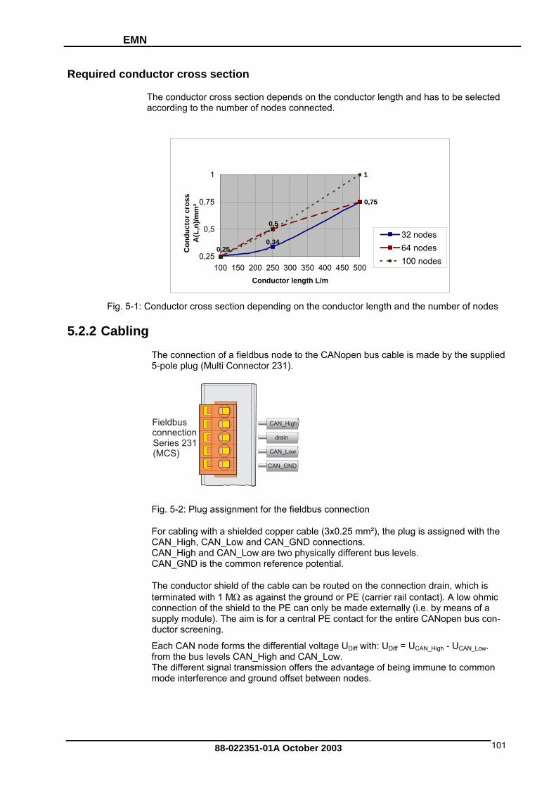
EMN
Required conductor cross section
The conductor cross section depends on the conductor length and has to be selected according to the number of nodes connected.
Fig. 5-1: Conductor cross section depending on the conductor length and the number of nodes
5.2.2 Cabling
bus node to the CANopen bus cable is made by the supplied -pole plug (Multi Connector 231).
0,75
1
0,340,25
0,5
0,25
0,5
0,75
1
100 150 200 250 300 350 400 450 500Conductor length L/m
Con
duct
or c
ross
A(L
,n)/m
m²
32 nodes64 nodes100 nodes
The connection of a field5
FieldbusconnectionSeries 231(MCS)
CAN_High
drain
CAN_Low
CAN_GND
Fig. 5-2: Plug assignment for the fieldbus connection
For cabling with a shielded copper cable (3x0.25 mm²), the plug is assigned with the CAN NCAN_High and CAN_Low are two physically different bus levels. CAN
The ab ection drain, which is terminated with 1 MΩ as agains w ohmic con shield to the Psupply module). The aim is for a central ductor screening.
Each CAN node forms the differential voltage UDiff with: UDiff = UCAN_High - UCAN_Low. from the bus levels CAN_High and CAN_Low. The different signal transmission offers the advantage of being immune to common mod interference and ground
_High, CAN_Low and CA _GND connections.
_GND is the common reference potential.
conductor shield of the c le can be routed on the connt the ground or PE (carrier rail contact). A lo
nection of the E can only be made externally (i.e. by means of a PE contact for the entire CANopen bus con-
e offset between nodes.
88-022351-01A October 2003 101

PIO Parker I/O-System
If the bus level is in the recessive status, the voltage between CAN_Low and CAN_GND is 2.5 V and also 2.5°This eans that the differential
If th bus level is in the dominaCAN GND is 1.5 V and 3.5°V bThe differential voltage is app
V between CAN_High and CAN_GND. voltage is 0 V. m
e _
nt status, the voltage between CAN_Low and etween CAN_High and CAN_GND.
n rox. 2 V.
Note WA
h n connecting subscribers, t mixed up. t i conductor ends, the bus with a matching
equired for very short conductor lengths.
ets
ensure that the data lines are nocable must always be connected
resistor of 120 Ohm to avoid reflections and, as a result, transmission problems. This is also r
CL+
M
S
17
18
22
750-3
07
87
65
43
21 ON
RT RT
CAN_High
CAN_Low
RT = 120 Ohm
Fig. 5-3: Connection principle of a fieldbus node to the CAN bus
88-022351-01A October 2003 102

EMN
Before starting the buscoupler on the nThe physical connection can be checkeany place. You have to remove all conn ces except for the termi-nating resistors.
etwork, the installation should be checked. d in the CAN fieldbus with an ohmmeter at ections to other devi
RT RT
CAN_High
CAN_Low
GND
RT = 120 Ohm
ohmmeter
leFig. 5-4: Measuring princip
to check the CAN bus prior to wiring
Measurement Value Meaning
infinite ok. GND and CAN_L
0 Short-circuit between GND and CAN_L
infinite o.k. GND and CAN_H
0 Short-circuit between GND and CAN_H
ca. s 60 Ω o.k., 2 terminal resistors in the bu
ca. resistor in the bus 120 Ω Only 1 terminal CAN_L and CAN_H
< 5 minal resistors in the bus
0 Ω More than 2 ter
The CAN bus is 2-wire bus and bus erroshort-circuit by the
r management can detect a cable break or a ric operation. asymmet
i
Further information The CiA provides documents regarding specificin the Internet under:
ations, especially cable specifications
http://www.can-cia.de
88-022351-01A October 2003 103
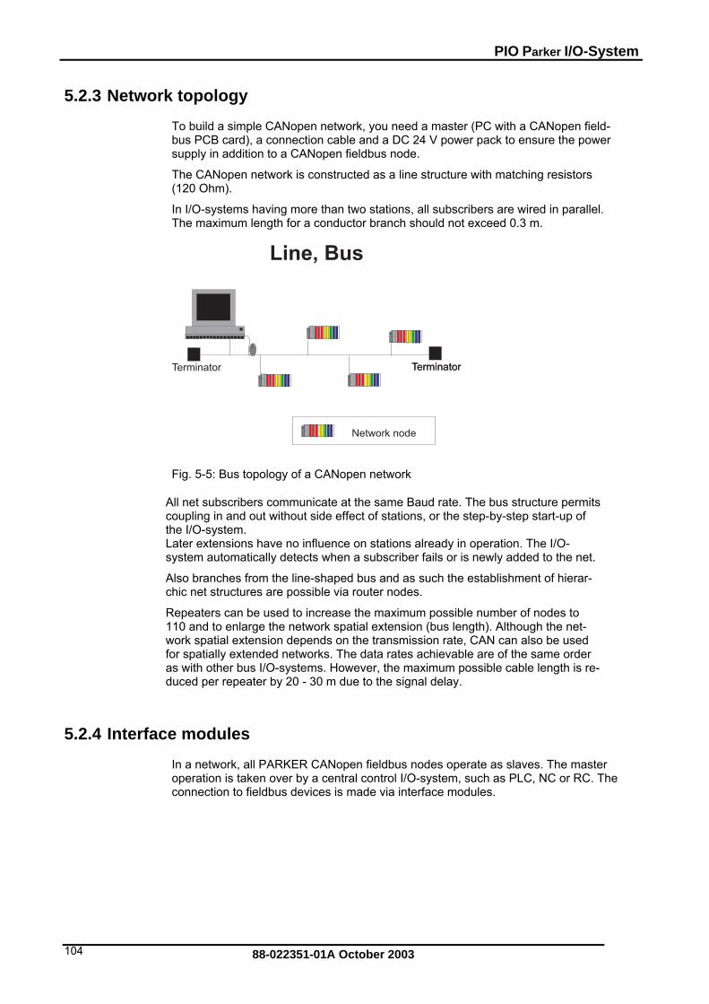
PIO Parker I/O-System
5.2.3 Network topology
To build a simple CANopen network, you need a master (PC with a CANopen field-bus PCB card), a connection cable and a DC 24 V power pack to ensure the power supply in addition to a CANopen fieldbus node.
The CANopen network is constructed as a line structure with matching resistors (120 Ohm).
In I/O-systems having more than two stations, all subscribers are wired in parallel. The maximum length for a conductor branch should not exceed 0.3 m.
Terminator Terminator
Line, Bus
Terminator
Network node
Fig. 5-5 n ne
All net subscribers communicate at the scoupling in and out without side effect of the I/O-system. Later extensions have no influence on st dy in operation. The I/O-system a a sub
Also branches from the line-shaped bus and as such the establishment of hierar-chic net structures are possible via router nodes.
Repeate can be used to increase the md atial e
work spatial extension depends on the transmission rate, CAN can also be used for spati ly extended networks. The datas with other bus I/O-systems. Howeverduced per repeater by 20 - 30 m due to t
5.2.4 Inter d les
twork, all PARKER CANopen fieldbus nodes operate as slaves. The master ion is taken over by a central control I/O-system, such as PLC, NC or RC. The
: Bus topology of a CANope twork
ame Baud rate. The bus structure permits stations, or the step-by-step start-up of
ations alreautomatically detects when scriber fails or is newly added to the net.
rs aximum possible number of nodes to 110 an to enlarge the network sp xtension (bus length). Although the net-
al a rates achievable are of the same order , the maximum possible cable length is re-he signal delay.
face mo u
In a neoperatconnection to fieldbus devices is made via interface modules.
88-022351-01A October 2003 104

EMN
5.3 Network mm nication With CANopen, data transmission, the ents, signalling of error states tc. takes place by means of communication objects. For this purpose, each commu-
network. The parameters required for the communication objects as well as the parameters
ement (NMT), for ges (EMCY), the communication profile O.
The PDOs (process data objects) are used for the transmission of real time data, and a obje
and writing.
5.3.1 Communication objects
Process Data O
PDOs contain real time data identifiers. The data telegrams consist bytes an individual sub-
assemblies, as required. Thperformed in a synchronizeto be drastically reduced perate. However, the various m"Object 0x1400– 0x141F, Receive PDO Communication Parameter").
PDO Protocol
his protocol is used to transmit data from/to the bus coupler without protocol over-r and the data field. No further protocol
information is contained in a PDO. The contents of the data are defined by the map-he communication parameters.
ipt PDO) and TxPDO (transmit PDO).
co utriggering of ev
enication object is assigned a clear COB-ID (Communication Object Identifier) in the
and data of the CANopen subscribers are filled in the object directory. Type and number of objects supported by the node depend on the individual fieldbus coupler. In addition to several special objects, i.e. for the network managsynchronization (SYNC) or for error messacontains the two object types PDO and SD
the SDOs (service dat cts) permit access to the object directory both for reading
bject - PDO
with high priorityof a maximum of 8 d can be interchanged among the
is data exchange can be optionally event controlled or d manner. The event controlled mode allows the bus load rmitting a high communication capacity at a low Baud odes can also be processed as a mix (see chapter
Thead. PDOs consist only of the CAN identifie
ping parameters and the transmission type by t
A differentiation is made between RxPDO (rece
Receive Process Data Object (RxPDO)
C
COB-ID
Data
8
= yy
0
Serverlient
F . 5 Pig -6: Rx DO
Transmit Process Data Object (TxPDO)
Client
RTR-Frame, COB ID = xx
COB-ID = xx
Data
0 8
Server
Fig. 5-7: TxPDO
88-022351-01A October 2003 105
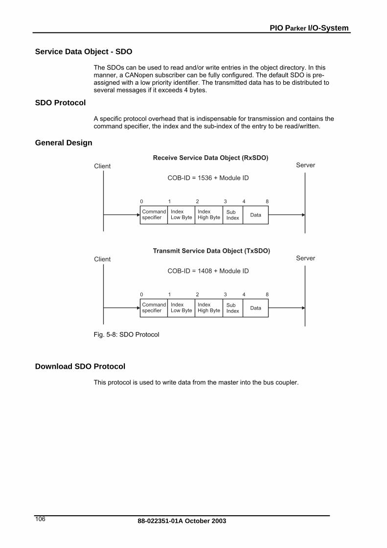
PIO Parker I/O-System
Service Data Object - SDO
T s can b o rea nd/or write . In this anner, a CANopen subscriber can be fully configured. The default SDO is pre-
with a low priority identifier. The transmitted data has to be distributed to
SDO Protocol
A specific protocol overhead that is indispensable for transmission and contains the command specifier, the index and the sub-index of the entry to be read/written.
he SDO e used t d a entries in the object directorymassignedseveral messages if it exceeds 4 bytes.
General Design
Client
Receive Service Data Object (RxSDO)Server
Transmit Service Data Object (TxSDO)
OB
COB-ID = 1408 + Module ID
DataSubIndex
Sub
IndexHigh Byte
Index
IndexLow Byte
IndexLow
Commandspecifier
Command
0 1 2
Server
C -ID = 1536 + Module ID
3 4 8
Client
0 1 2 3 4 8
DataIndexHigh ByteBytespecifier
F DO Prig. 5-8: S otocol
Download SDO Protocol
This protocol is used to write data from the master into the bus coupler.
88-022351-01A October 2003 106

EMN
Initiate SDO Download
This protocol is used to initiate the data transmission from the master to the bus cou-pler. When transmitting data of max. 4 bytes, these are also transmitted within the protocol.
Client
Client
Initiate SDO Download
Server
Initiate SDO Download
Data
Data
ccs = 1 x
x x x
n e
e
s m
ms
indication
response
0
.0
.0
.5
.5
.4
.4
.3 .2
.3 .2
.1
.1
1
1
4
4
8
8
Server
request
0
.7 .6
scs = 3
confirm .7 .6
Fig. 5-9: Initiate SDO
ccs: client command specifier 1: initiate download request scs: server command specifier 3: initiate download response n: only valid if e = 1
and s = 1, otherwise 0. If n is valid, it displays the number of bytes which do not contain any data. Example: 3 data bytes, e = 1 and s = 1, n = 4 - 3 = 1
e: transfer type 0: normal transfer, number of the bytes to be written >= 5 byte
1: expedited transfer, number of the bytes to be written < 5 byte
s: size indicator 0: data set size is not displayed 1: data set size is displayed s is always 1 m: multiplexor Index and Sub-Index of object directory Index, Low Byte : Byte #1 Index, High Byte: Byte #2 Sub-Index: Byte #3 d: data e = 0, s = 0: d is reserved for further use of CiA e = 0, s = 1: d contains the number of bytes for download Byte 4 contains the LSB and Byte 7 contains the MSB. e = 1: d contains the data X: Not used, always 0 reserved: Reserved for further use of CiA
88-022351-01A October 2003 107

PIO Parker I/O-System
Download SDO Segment
This protocoing the „Initi
l is used to transmit more than 4 data, i. e. this follows after fully process-ate SDO Download Protocol" which initiates the data transmissions.
Client
Client
Download SDO Segment
Server
Download SDO Segment
Segment data
reserved
ccs = 0
scs = 1
t
t x
n c
request
confirm
indication
response
0
0
.0
.0
.7
.7
.6
.6
.5
.5
.4
.4
.3 .2
.3 .2
.1
.1
1
1
8
8
Server
Fig. 5-10: Download SDO Segment
ccs: client command specifier 0: download segment request scs: server command speci- 1: downl
fier oad segment response
seg-data Contains the data to be transmitted.
The meaning of the data is determined by the application.
n: Displays the number of bytes not containing any data. n is 0 if no segment size is dis-played.
c: Indicates whether or not a download is necessary for further data.
0: There is more data to be downloaded.
1: There is no more data to be downloaded. t: Toggle Bit This bit must be able to toggle for each
segment for which a download is made. The first segment zeroes the toggle bit. The tog-gle bit is identical both for the enquiry and the reply message.
X: Not used, always 0 reserved: Reserved for further use of CiA
tocol
This protocol is used to read data out of the bus coupler.
Upload SDO Pro
88-022351-01A October 2003 108

EMN
Initiate SDO Up
roto-col. When transmitting data of max. 4 bytes, these are also transmitted within the pro-
ol.
load
The data transmission from the bus coupler to the master is initiated with this p
toc
Client
Initiate SDO Upload
Server
Client Server
Initiate SDO Upload
reserved
Data
ccs = 2
scs = 2
x
x n e
m
ms
indication
response.0.7 .6 .5 .4 .3 .2 .1
1 4
8
8
request .0.7 .6 .5 .4 .3 .2 .1
40 1
confirm
0
Fig. 5-11: Initiate SDO Upload
ccs: Client command specifier 2: initiate upload request scs: Server command specifier 2: initiate upload response n: is only valid if e = 1 and s
= 1, otherwise 0. If n is valid, it displays the number of bytes in d which do not contain any data. The bytes [8-n, 7] do not contain segment data.
e: transfer type 0: normal transfer, number of bytes to be written >= 5 bytes
1: expedited transfer, number of bytes to be written < 5 bytes
s: size indicator 0: the number of bytes to be transmitted is not displayed 1: the number of bytes to be transmitted is displayed (de-
pending on the number of bytes) m: multiplexor Index and sub-index of the object directory: Index, Low Byte : Byte #1 Index, High Byte: Byte #2 Sub-Index: Byte #3 d: data e = 0, s = 0: d is reserved for further use of CiA e = 0, s = 1: d contains the number of bytes for download Byte 4 contains the LSB and Byte 7 contains the MSB. e = 1: d contains the data X: Not used, always 0
88-022351-01A October 2003 109

PIO Parker I/O-System
reserved: Reserved for further use of CiA
Upload SDO Segment
This protocol is used if more than 4 data is transmitted, i.e. this follows after fully processing the „Initiate Upload Protocol" which initiates the data transmissions.
Client
Upload SDO Segment
Client Server
Upload SDO Segment
reserved
Segment data
ccs = 3
scs = 0
t
t x c
x
request
confirm
indication
response
0
.0
.0
.7
.7
.6
.6
.5
.5
.4
.4
.3 .2
.3 .2
.1
.1
1 8
Server
0 1 8
Fig. 5-12: Upload SDO Segment
ccs: ier 3: download segment request Client command specifscs: Server command specifier 0: download segment response t: Toggle bit This bit has to change for each segment for
e tog-gle bit is identical both for the enquiry and the reply.
which an upload is made. The toggle bit has to be zeroed for the first segment. Th
c: Indicates whether further
upload
0: there are more segments to be uploaded segments are present for the
ng 1:there are no more segments for uploadiseg-data Contains the data to be
transmitted. The meaning of the data is determined by the application.
n: hich do not contain data. Bytes [8-n, 7] do not contained data. N is 0 if no segment size is displayed.
Displays the number of bytes w
X: Not used, always 0 reserved: Reserved for further use of CiA
88-022351-01A October 2003 110

EMN
Abort SDO Tran
ing transmission.
sfer
This protocol is used in the event of errors occurring dur
Client
Abord SDO Transfer
Datacs = 4 x m
indication
0
.0.7 .6 .5 .4 .3 .2 .1
1 4 8
Server
request
Fig. 5-13: Abort SDO Transfer
4: abort domain transfer cs: command specifier m: multiplexor Index and Sub-Index of Object directory: X: Not used, always 0 Data 4 Byte Error Code Application specific data about the reasons
for the abort.
SDO Examples
The following are 4 SDO examples, the data is being displayed in hexadecimal. These examples show the handling of SDOs on the CAN message level and can be used if the SDO protocol is to be implemented on a CAN card.
A message is subdivided into 4 columns:
1. column Direction M->BC = message is sent by the master to the bus cou-pler. BC->M = message is sent by the bus coupler to the mas-ter.
2. column CAN Identifier 3. column Frame Type D = Data frame
R = RTR frame 4. column Data Data bytes of the CAN message
maximum of 8 data bytes can be transmitted in a CAN essage. The individual bytes are separated by spaces.
Entries having the value XX have no meaning, but must be existing. The values should be zeroed for a better understanding.
ch are dependent on the configura-
Am
Entries in the reply from the bus coupler having the value DD contain data, whition.
Example 1: Read Index 0x1000 Sub-Index 0; Device Type
Index 0x1000 returns 4 bytes. The expedited transfer mode is used for transmission.
Direction CAN Id Frame Type Data byte 0-7
88-022351-01A October 2003 111

PIO Parker I/O-System
M->BC 0x601 D 0x40 00 10 00 XX XX XX XX
BC->M 0x581 D 0x43 00 10 00 91 01 DD 00 Result: Data bytes 4 and 5: 91 01 Sequence Low Byte, High Byte rotation: 0x0191 = 401 Device Profile Nu
a bytes 6 and 7: DD 00 Sequence Low Byte, High Byte rotation
mber
Dat
Example 2: Read Inde 0
Index 0x1008 returns more than 4 bytes. The normal transfer mode is used for d.
x x1008 Sub-Index 0; Manufacturer Device Name
transmission in which case 2 messages per mode are transmitte
Direction CAN Id Frame Type Data byte 0-7
M->BC 0x601 D 0x40 08 10 00 XX XX XX XX
BC->M 0x581 D 0x41 08 10 00 07 00 00 00
M->BC 0x601 D 0x60 XX XX XX XX XX XX XX
BC->M 0x581 D 0x01 37 35 30 2D 33 33 37 Result: The first reply from the bus coupler informs the master of the number of data to be transmitted (0x00000007 Byte). In the second message, the bus coupler supplies thearticle number in the ASCII format (hex represen
tation)
Example 3: Read Index 0x2000 Sub-Index 1; Fi
The signals of the digital input modules art
„PIO-337“.
rst 8 bit digital input block
e saved in index 0x2000. 8 bits each are assigned to a group and can be read as from sub index 1. In this example, the inpuvalue of the first 8 bit group is read via an SDO message.
Direction CAN Id Frame Type Data byte 0-7
M->BC 0x601 D 0x40 00 20 01 XX XX XX XX
BC->M 0x581 D 0x4F 00 20 01 02 XX XX XX Result:
thIn the 5 byte of the CAN message, the bus couplgroup of 8 bits. In
er returns the status of the first this set. Bytes 5-7 are without meaning.
Example 4: Write Index 0x2100 Sub-Index 1; Fi
of t in index 0x2100. 8 bits to as from sub index 1. In alu ritten into the outputs of the first 8 bit digital output
case the 2nd bit is
rst 8 bit digital output block
The output values each are assigned
he digital output modules are saved a group and can be read and written
this example, the v e 0xFF is wgroup.
Direction CAN Id Frame Type Data byte 0-7
M->BC 0x60 XX 1 D 0x2F 00 21 01 FF XX XX
BC->M 0x58 0x60 00 21 01 XX XX XX XX 1 D
88-022351-01A October 2003 112

EMN
Result: The outputs of the first 8 bit digital output modules are set.
Synchronization
hese objects allow the synchronization of all network subscribers. Corresponding network subscribers to process their input
data or to update the outputs upon the arrival of a SYNC object. In this manner cyclical transmission of a SYNC object ensures that all network sub-
SYNC Protocol
Object - SYNC
Tconfiguration of the PDOs can initiate the
scribers will process their process data simultaneously.
Sync Producer
Sync Protokoll
COB-ID = 128
L = 0
Sync Consumer(s)
indication(s)request
Fig. 5-14: SYNC Protocol
Emergency Obj t
Emis re sen e erroerro
EMCY Protocol
Y Consumer(s)
ec (EMCY)
ergency objects are triggered by an internal error situation such as i.e. a module moved during operation, or a module signals an error. The bus coupler thends an emergency object to all connected devices (Broadcast), to broadcast thr occurred. The informed bus subscribers can then react accordingly by suitable r correction measures.
CY Producer
EMCY Protokoll
EMCEM
requestindication(s)
MEREEC ER
0 2 3 8
Fig. 5-15: EMCY Protocol
88-022351-01A October 2003 113

PIO Parker I/O-System
5.3.2 Communic
CANopen state diagram
T d ram des shows t -tion states and possible transitions related to the CAN communication.
Operational
Stopped
ation states of a CANopen fieldbus coupler
he status iag cribed in the following figure he individual communica
Power On
Initialization
Pre-Operational
Error
SRemoteNode
Start Remote Node
Stop Remote Node
EnterPre-Operational
deResetCommunication
Initialisation finished
Reset No
Stop Remote Node
Enter Pre-Operational
tart
Fig. 5-16: State diagram of the fieldbus coupler
INITIALIZATION
F llowing a er On o the utomati-ll ALIZATION status. this status, the bus coupler performs a self-
che prostored configuration, and the object directory initialized. If no errors are detected dur-ing the initialization phase the bus coupler automatically changes to the pre-operational status. If errors were found, a change to the STOP status takes place.
D ia tion, the ge and chigher frequency. If initialization and the change to the pre-operational status have been successfully completed, the I/O LED is lit green and the RUN LED blinks. If er-rors have occurred (i.e. no end module connected) the I/O LED indicates the error type by a red blinking sequence (see LED status display). In this case, the STOP L D is lit red
PRE-OPERATIONAL
In this status, communication can be mn t possible he SDOs e e ject direc-
ries permitting for instance to re-configure the bus coupler by means of the configu-s, IDs etc. can in this manner be adapted
to the required conditions. The newly configured configuration can be saved in flash.
o pow r a reset (module ID unequal 0), bus coupler is aca y in the INITI In
ck to check all functions of its components and the communication interface. Thecess image is created on the basis of the connected modules and a possibly
uring init liza I/O-LED starts blinking oran hanges to red at its
E .
ade via SDOs. Communication via PDOs is o . T allow for reading and writing in th ntries of the ob
toration tool. Mapping, bus coupler parameter
88-022351-01A October 2003 114

EMN
A hange from ns of the NMT service Start_Remote_Node. e pre-operational status the I/O LED is lit green and the RUN LED blinks.
c the pre-operational status to the operational status is performed by meaIn th
OPERATIONAL
T a ws comm Os, it dodifferent configurations. It is, for instance, not allowed to chapresence of a valid PDO. For a detailed description, please refer to the correspond-ing entries in the object directory. The change from the operational status to the pre-operational status is performed w h the NM ervice EIn the operational status, the I/O and the RUN LED are lit.
STOPPED
top_Remote_Node was received or if a fatal internal error has occurred (i.e. module
ices andYou can quit the Stopped status via the NMT services Start_Remote_Node_Indication, Enter_Pre_Operational_State and Reset_Node. The Stop LED is lit in the Stopped status.
his status llo unication via SDOs and PD es, however, not allow nge the COB ID in the
it T s nter_Pre_Operational_State.
The Stopped status reflects an error status. S
This is the case if the NMT service
was removed during operation). This status does not allow communication via SDOs or PDOs. Only the NMT serv
the Node Guarding/Heartbeat (if activated) are performed.
88-022351-01A October 2003 115

PIO Parker I/O-System
5.3.3 Network M
Module Control Protocols
T m er can u he statufollowing states are defined: INITIALIZING, PRE-OPERATIONAL, OPERATIONAL and STOPPED. It is possible to change the status of all nodes with one command or to change the status of each node individually.
Start Remote Node
This service is used to change the NMT Slav
anagement Objects
he NMT ast se these protocols to check t s of the NMT slave. The
e (bus coupler) status to OPERATIONAL.
N
Start Remote Node
NMT Slave(s)MT Master
reqindication(s)
CS Node
0 1
uest
= 1 ID
COB-ID = 0
Fig. 5-17: Start Remote Nodex
Stop Remote Node
This service is used to change the NMT Slave (bus coupler) status to STOPPED.
NMT Master
Stop Remote Node
NMT Slave(s)
requestindication(s)
CS= 2
COB-ID = 0
NodeID
0 1
Fig. 5-18: Stop Remote Nodex
88-022351-01A October 2003 116
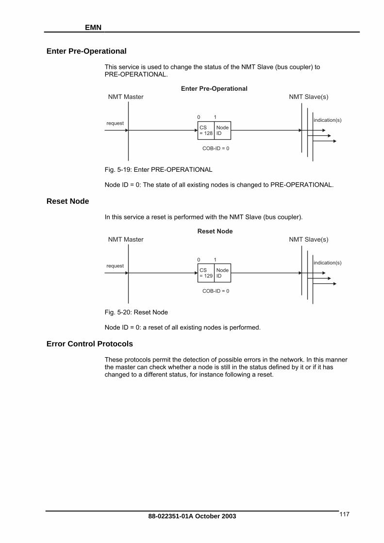
EMN
Enter Pre-Operational
This service is used to change the status of the NMT Slave (bus coupler) to PRE-OPERATIONAL.
Enter Pre-Operational
NMT Slave(s)NMT Master
requestindication(s)
CS Node= 128 ID
0 1
COB-ID = 0
Fig. 5-19: Enter PRE-OPERATIONAL
Node ID = 0: The state of all existing nodes is changed to PRE-OPERATIONAL.
Reset Node
NMT Slave(s)
In this service a reset is performed with the NMT Slave (bus coupler).
NMT Master
Reset Node
requestindicatio
CS Node
0n(s)
= 129 ID
COB-ID = 0
1
Fig. 5-20
D = 0: a reset of all existing nodes is performed.
Error Control Protocols
p rmit the detec le errors in the network. In this manner the status defined by it or if it has
d r e followin
: Reset Node
Node I
These rotocols pe tion of possibthe master can check whether a node is still inchange to a different status, fo instanc g a reset.
88-022351-01A October 2003 117

PIO Parker I/O-System
Node Guarding Protocol
By means of Node Guarding, the NMT slave is cyclically requested via an RTR frame t its rren ditiona f detects hether or not the NMT
ill o erate . o send lave st
cup
t status. Ads correctly
l toggling o a bit ws
NMT Master
Reset Node
NMT Slave
request
request
confimation
confimation
indication
Network Even*if guarding errort
*Node Event
*
.7Toggle-Bit
Toggle-Bit
Node State
Nod
Remote Frame
.6
.6
.0
indicationRemote Frame
indication
indication
response
response.7
e State
.0
Heartbeat Proto o
monitoring without RTR frames. A heartbeat generator cyclically generates a heartbeat message received by n subscribers. The heartbeat message contains the coding of the current g ator sta
Heartbeat Consumer
Fig. 5-21: Node Guarding Protocol
c l
This protocol allows
ener tus.
Heartb
Heartbeat Protocol
eat Producer
request
request
HeaProducerTim
HeartbeatConsumerTime
HeartbeatEvent
rtbeat
e
indication(s)
indication(s)
indication
0 … 7 s
0 … 7 s
F 5-22: Hearig. tbeat Protocol
88-022351-01A October 2003 118

EMN
Bootup Protocol
This protocol shows that the NMT slave has changed its status from INITIALIZING to PRE-OPERATIONAL. This is performed after a hardware/software reset or following the service reset code.
NMT Slave NMT Master
request indication
0
0
COB-ID = 1792 + Node-ID
Fig. 5-23: Bootup Protocol
5.3.4 Object D
e all configura-polled. The directory organization is by
• omm i file Area (In x1000 – p ile c ram nt f ANope ation. This
facturer Specific Profile Area (Index 0x2000 – 0x5FFF) implement his own company specific
jects.
• Profile Area (Index 0x9FFF) This profile contains all objects which are assisted by a certain device profile. The bus coupler assists the device profile DS-401 (Device Profile for Generic I/O
In the object directory, a logical addressing scheme is used for the access to com-munication and device parameters, data and func ch e directory i ied y a ich he addres f the table. A maxi-mum of 65536 entries are permitted.
d by means of an 8 bit sub-index. The sub-index indicates the individual column address
256 entries.
E entry i
•
• an access attribute indicating whether the entry is only read, only write or read and write.
irectory
The object directory is the central point of a CANopen subscriber whertion information and data is stored and can be means of tables and contains three areas of CANopen objects:
C unicat on Pro dex 0 0x1FFF)This rof ontains all pa eters releva or C n communicarea is identical for all CANopen subscribers.
• ManuIn this profile, each manufacturer can ob
Standardized Device 0x6000 –
Modules)
tions. Ea entry into ths identif b 16 bit index wh indicates t row s o
If an object is composed of several components, the components are identifie
of the table allowing a maximum of
ach cons sts of:
an object name describing the object function,
• a data type attribute defining the data type of the entry, and
88-022351-01A October 2003 119

PIO Parker I/O-System
The sub-index 0 indicates the max. numbeThe data is coded in the following sub-indexes.
r of the following sub-indexes.
Index (hexadecimal) Object
0x0000 Not used
0x0001 – 0x001F Static data types
0x0020 – 0x003F Complex data types
0x0040 – 0x005F Manufacturer specific data types
0 0 07F cific static data types x0060 – x0 Profile spe
0x0080 – 0x009F Profile specific complex data types
0x00A0 – 0x0FFF Reserved
0x1000 – 0x1FFF Communication profile (DS-301)
0 0 – 0 anufacture ific parx200 x5FFF M r spec ameters
0 FF eters r device files x6000 – 0x9 F Param from standa dized pro
0xA000 – 0xFFFF Reserved
Table 5-2: Structure of the CANopen object directory
ructure is designed for the worst case. Object entries that can-not be used because of the connected module configuration are deactivated.
Initialization
urrently connected module
ialized.
In every other case, object directory will be assigned a default configuration.
Default configura
Initialization Co
and as such the process described there is used. The first 4 Rx-/TxPDOs are defined as default PDOs. If more
ll
available, a continuation is only made with PDO 5, even if no analog modules exist. PDO 2 to 4 will then remain unused. Furthermore, only one data type is used as a default entry for a PDO, in other words, if a 3 byte and a 4 byte module exists, then a default is entered for each of the 2 PDOs.
The object directory st
The connected module configuration is determined following power On.
If a customer-specific configuration was saved and if the cconfiguration coincides with the one last saved, the object directory with this saved configuration will be init
tion
mmunication Profile Area
All objects of this profile assisted by the bus coupler are initialized according to the default values of DS 301 (CANopen Application Layer and Communication Profile).
• Entry of the default mapping parameters: Pre-assignment of the mapping parameters depends on the device profile used. The bus coupler assists the DS 401 profile,
inputs/outputs exist at the bus coupler than can be covered with the default PDOs, from Rx-/TxPDO 5 all remaining I/Os are entered. First all digital, then aanalog I/Os are entered. If more than 64 digital I/Os per input/output are
88-022351-01A October 2003 120

EMN
• 1. RxPcontains maximum the first 8x8 digital outputs. If no digital outputs exist, the subindex 0 has the default value 0, and this PDO is not used with its default value.
DO:
Idx S-Idx Description Default Value
0x1600 0 Number of mapped objects None, possible values:
0: no digital output block
ital output cks
1..8: 1..8 digblo
1 1. mapped u k 6200 01 08 digital outp t bloc 0x
2 ed ut ck 2. mapp digital outp blo 0x6200 02 08
: : :
8 8. mapped u k 6200 08 08 digital outp t bloc 0x
• 2. RxPDO: alog output. If no 16 bit analog outputs exist,
the sub index 0 has the default value 0, and this PDO is not used with its default contains max. the 1st to 4th 16 bit an
value.
Idx S-Idx Description Default Value
0x1601 0 Number of mapped objects None, possible values:
0: no analog output
1..4: 1..4 analog out-puts
1 1. mapped 16 bit analog output 0x6411 01 10
2 2. mapped 16 bit analog output 0x6411 02 10
3 3. mapped 16 bit analog output 0x6411 03 10
4 4. mapped 16 bit analog output 0x6411 04 10
• 3. RxPDO: contains maximum the 5th to 8th bit analog output. If more than 4 16 bit analog outputs exist, the sub index 0 has the default value 0, and this PDO is not usedwith its default value.
Idx S-Idx Description Default Value
0x1602 0 Number of mapped objects None, possible values:
0: no analog output
1..4: 1..4 analog out-puts
1 5. mapped 16 bit analog output 0x6411 05 10
2 6. mapped 16 bit analog output 0x6411 06 10
3 7. mapped 16 bit analog output 0x6411 07 10
4 8. mapped 16 bit analog output 0x6411 08 10
88-022351-01A October 2003 121

PIO Parker I/O-System
• 4. RxPDO: contains maximum the 9th to 12th 16 bit analog output. If not more than 8 16 bit
ault value 0, and this PDO is not analog outputs exist, the sub index 0 has the defused with its default value.
Idx S-Idx Description Default Value
0x1603 0
0: no analog output
Number of mapped objects None, possible values:
1..4: 1..4 analog out-puts
1 9. mapped 16 bit analog output 0x6411 09 10
2 10. mapped 16 bit analog output 0x6411 0A 10
3 11. mapped 16 bit analog output 0x6411 0B 10
4 12. mapped 16 bit analog output 0 0x6411 0C 1
• 1. TxPDO: ains maximum the first 8x8 digital inputs. If no digital inputs exist, the sub
index 0 has the default value 0, and this PDO is not used with its default value. cont
Idx S-Idx Description Default Value
0x1A00 0 Number of mapped objects None, possible values:
0: no digital input block
1..8: 1..8 digital input blocks
1 1. mapped digital input block 0x6000 01 08
2 2. mapped digital input block 0x6000 02 08
: : :
8 8. mapped digital input block 0x6000 08 08
• 2. TxPDO: contains maximum the 1 to 4 16 bit analog input. If no 16 bit analog inputs exist, the sub index 0 has the default value 0, and this PDO is not used with its default value.
st th
Idx S-Idx Description Default Value
0x1A01 0 Number of mapped objects None, possible values:
nalog input
1..4: 1..4 analog inputs
0: no a
1 1. mapped 16 bit analog input 0x6401 01 10
2 2. mapped 16 bit analog input 0x6401 02 10
3 3. mapped 16 bit analog input 0x6401 03 10
4 4. mapped 16 bit analog input 0x6401 04 10
88-022351-01A October 2003 122

EMN
• 3. TxPDO: contains maximum the 5th to 8th 16 bit analog input. If not more than 4 16 bit nalog s the sub index 0 he default value 0, and this PDO is not a input exist, has t
used with its default value.
Idx S-Idx Description Default Value
0x1A02 p None, possible values:
0: no analog input
1..4: 1..4 analog inputs
0 Number of ma ped objects
1 5. mapped 16 bit analog input 0x6401 05 10
2 6. mapped 16 bit analog input 0x6401 06 10
3 7. mapped 16 bit analog input 0x6401 07 10
4 8. mapped 16 bit analog input 0x6401 08 10
• xPDO: s maxim m the 9th to 12th 16 bit analog input. If not more than 8 16 bit inputs exist, the sub index 0 has the default value 0, and this PDO is not
used with its default value.
4. Tcontainanalog
u
Idx S-Idx Description Default Value
0x1A03 0 Number of mapped objects None, possible values:
0: no analog input
1..4: 1..4 analog inputs
1 9. mapped 16 bit analog input 0x6401 09 10
2 10. mapped 16 bit analog input 0x6401 0A 10
3 11. mapped 16 bit analog input 0x6401 0B 10
12. mapped 16 alog inp x64 bit an ut 0 401 0C 10
• Initiali ion pecif rThis area is initialized as described in the object directory.
e Profile Area
zat Manufacturer S ic Profile A ea
• Initialization Standardized DevicAll supported objects are initialized, as defined in the DS 401 standard.
88-022351-01A October 2003 123

PIO Parker I/O-System
Communication Profile Area
The following table contains all objects of the communication profile supported by the bus coupler.
Idx Name Type Meaning See on page
0x1000 Device Unsigned32 Device e 125 Type Profil
0 001 or Re t 5 x1 Err gister Unsigned8 Errors are bi coded (DS401) 12
0x1003 Pre-defined Error Field Array Unsigned32 Storage of the last 20 eoccurred
rrors 126
0x1005 COB-ID SYNC message Unsigned32 COB-ID of the SYNC object 126
0x1006 Communication Cycle Period Unsigned32 Max. time betw
messages een 2 SYNC 126
0x1008 Manufacturer Device Name Visible String Device name 126
0x1009 Manufacturer Hardware Version Visible String Hardware version 127
0 cturer Software Software v 127 x100A Manufa
Version Visible String ersion
0x100C Guard Time Unsigned16 Time for “Life Guarding Protocol“ 127
0x100D Life Time Factor Unsigned8 Life Time Factor 127
0x1010 rs nsigned umber of store parameters 127 Store Paramete Array U 32 max. n
0 store r ed 128 32 Parameter to restore the default configuration x1011 Re default Paramete Array Unsign
0 COB-ID Emergency Object Unsigned32 COB-ID for the emergency Ob-ject 129 x1014
0x1015 Min. time between 2 EMCY 129 Inhibit Time EMCY Unsigned32 messages
0x1016 Consum Array Unsigned32 Heartbeat monitoring time 130 er Heartbeat Time
0x1017 Producer Heartbeat Time Unsigned16 een 2 generated Heartbeat messages 130 Time betw
0x1018 Identity Object Record Identity Device information 130
0x1200 to 0
Server SDO Record S ameter Parameter for the Server SDO 131
x1201 Parameter DO Par
0
0x141F tion Parameter PDO Parameter Communication parameter for the Receive PDO 131
x1400 Receive PDO Communica-to Record
0x1600 to Receive PDO Mapping Record Mapping paramete
0x161F Parameter PDO Mapping r for the Re-
ceive PDO 132
0x1800 to0x181F Par ete 133 Transmit PDO Communica-
tion ameter Record PDO Param r the Transmit PDO
Communication parameter for
0to0x1A1F
nsmit PDO Mapping rameter 134
x1A00 Tra
PaRecord PDO Mapping
Mapping parameter for the Transmit PDO
88-022351-01A October 2003 124
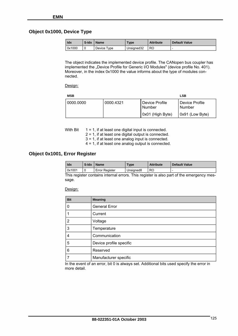
EMN
Object 0x1000, Device Type
Idx S-Idx Name Type Attribute Default Value
0x1000 0 D U - evice Type nsigned32 RO
s The object indicates the implemented device profile. The CANopen bus coupler haimplemented the „Device Profile for Generic I/O Modules" (device profile No. 401). Moreover, in the index 0x1000 the value informs about the type of modules con-nected.
Design:
MSB
0000.00
LSB
00 0000.4321 Device Profile
0 Byte)
Device Profile Number
w Byte)
Number
0x 1 (High 0x91 (Lo
With Bit 1 = 1, if at least one digital input is connected. = 1 f at lea one d ital ou ut is 3 = 1, if at least one analog input is 4 = 1, if at least one analog output is connected.
Object 0x1001, Error Register
2 , i st ig tp connected. connected.
Idx S-Idx Name Type Attribute Default Value
0x1001 rror Register - 0 E Unsigned8 RO This register contains internal errors. This register is also part of the emergency mes-sage.
Design:
Bit Meaning
0 General Error
1 Current
2 Voltage
3 Temperature
4 Communication
5 Device profile specific
6 Reserved
7 Manufacturer specific In the event of an error, bit 0 is always set. Additional bits used specify the error in more detail.
88-022351-01A October 2003 125

PIO Parker I/O-System
Object 0x1003, Pre-defined Error Field
Idx S-Idx Name Type Attribute Default Value
0x1003 0 Number of Erro ed8 RW rs Unsign 0 1 Standard Error Field Unsigned32 RO - : : : : : 20 Standard Error Field Unsigned32 RO -
T ndex 0 contains the new error occurs, i ed in sub-index wn by one s ex. A max. of 20 error d. Should more than 20 errors oc-cur, each time the error conta
Design Standard Error Field:
he sub-i errors currently stored in the field. If at will be enter 1, and all errors already existing moved doub-ind entries are supporte
ined in sub-index 20 is written over.
Bit31 Bit16 Bit15 Bit0
Additional Information Error code The additional information corresponds to the first 2 bytes of the additional code of the Emergency telegram. The error code coincides with the error code in the Emer-gency telegram.
The complete error memory is deleted by writing a „0" in sub-index 0.
Object 0x1005, COB-ID SYNC message
Idx S-Idx Name Type Attribute Default Value
0x1005 000080 0 COB-ID SYNC Unsigned32 RW 0x00T e object define ID for n on mess
Design:
h s the COB the synchro izati age.
Bit31 Bit11 Bit10 Bit0
Reserved (always 0) COB-ID
Object 0x1006, Communication Cycle Period
Idx S-Idx Name Type Attribute Default Value
0x1006 0 Communication Unsigned32 RW 0 Cycle Period
The object defines the max. time in µs for two subsequent SYNC messages. The in-ternal resolution is 2ms. If the value is 0, no SYNC monitoring is performed.
Object 0x1008, Manufacturer Device Name
Idx S-Idx Name Type Attribute Default Value
0x1008 0 Manufacturer De-vice Name
Visible String RO PIO-337
The object indicates the device name of the bus coupler.
88-022351-01A October 2003 126

EMN
O xbject 0 1009, Manufacturer Hardware Version
Idx S-Idx Name Type Attribute Default Value
0x1009 0 Manufacturer Visible String RO Current HW-Version Hardware Version
The object indicates the current hardware version of the bus coupler.
Object 0x100A, Manufacturer Software Version
Idx S-Idx Name Type Attribute Default Value
0x100A 0 Manufacturer Soft-ware Version
Visible String RO Current SW-Version
The object indicates the current software version of the bus coupler.
Object 0x100C, Guard Time
Idx S-Idx Name Type Attribute Default Value
0x100C 0 Guar signed16 RWd Time Un 0 The object indicates the Guar milli-seconds. T master cyclically in-
rrogates the NMT slave for its status. The time between two interrogations is Guard Time.
Object 0x100D, Life Time Factor
ding Time in An NMtetermed
Idx S-Idx Name Type Attribute Default Value
0x100D 0 Lifetime Factor Unsigned8 RW 0 The life Time Factor is part of f it was interrogated within the N e multiplied with the life time
ctor). If not, the slave works on the basis that the NMT master is no longer in its Life Guarding Event.
o, no monitoring will take place.
Object 0x1010,
the Node Guarding Protocol. The NMT slave checks iode Life Time (Guardtim
fanormal operation. It then triggers a
If the node life time is zer
Store Parameters
Idx S-Idx Name Type Attribute Default Value
0x1010 0 Max. supported Sub-Index
Unsigned8 RO 1
1 Store all Parameter Unsigned32 RW 1 This object allows to permanently store the settings made by the user. For this pur-pose, the signature „save" (lower case letters ASCII - MSB – 0x65 76 61 73 - LSB)
y telegram is sent. Communication remains possible during storage by ans s. An error messa a re new storage attempt only o
when the previous one was not yet finished. It is also not possible to trigger theage function for as long as „Restore" is active.
As soon as a setting is stored, th ency “Changed HW configuration” is not n e bus couple rted up again without changing the module
must be written into the index 0x1010 sub index 1. The storing process runs in the background and takes approx. 2-3 seconds. When the storing process is finished, the SDO replme of SDO ge as sult of a ccurs,
stor-
e Emergsent aconfigu
y longer if thration.
r is sta
88-022351-01A October 2003 127

PIO Parker I/O-System
Attention If following the storage of a configuration only the module ID is changed via the DIP switch, the saved configuration is continued l module I specific entries in the object directory the „rw" attribute) signal with the o ues
to be used. In other words, al D(objects that are module ID dependent and have
ld val . (i.e. Emergency ID,...)
Object 0x1011, Restore default Parameters
Idx S-Idx Name Type Attribute Default Value
0x1011 0 Max. supported Sub-Index
edUnsign 8 RO 4
1 Set all parameters on default value
edUnsign 32 RW 1
2 - Unsigned32 RW 0 3 - edUnsign 32 RW 0
lues once
Unsigned32 RW 1 4 Set all parameters on default va
This object allows to reset the us d lt values
Sub-indexes 2 and 3 are not supported.
ssed ackground and takes approx. 2-3 seconds When the performance is finished, the SDO reply message is sent. Communication
ued during perform in only trippe
o not possible to tr lo ve" is ac
Sub-index 1 - Permanent entry of default p e
letters ASCII - MSB 0x64 0x61 0x6F 0x6C LSB) into the index 0x1011 sub-index 1 entails loading of the standard factory set-tings after the following Power ON and each further Power On (until the next SAVE command is given).
Sub-index 4 – On-off entry of default parameters
Writing the signature „load" (lower case letters ASCII - MSB 0x64 0x61 0x6F 0x6C LSB) into the index 0x1011 sub-index 4 entails loading of the standard factory set-tings once only after the following Power ON. The saved configuration is re-loaded af-ter each further Power ON. This feature can, for instance, be used during the devel-opment phase in order to quickly obtain a behavior comparison of saved and default configurations without having to re-set and re-store all parameters each time.
er store parameters to the original defau .
The load command is proce in the b .
can be contin ance us g SDOs. An error message is dwith another attempt to send a load command,pleted.
if the previous one is not yet com-ad command for as long as „Sa It is als igger a -
tive.
aram ters
Writing the signature „load" (lower case
88-022351-01A October 2003 128

EMN
Sequence:
replace configuration once by default configuration
-> load (Index 0x1011, sub-index 4)
t
-> default values f the load 10 sub-in x 4) command is not permitted in this
status!)
-> stored configuration
bject x101 Emerg je
-> Rese
(re-use o (index 0x 11, de
-> Reset
O 0 4, COB-ID ency Ob ct
Idx S-Idx Name Type Attribute Default Value
0x1014 0 COB ID EMCY Unsigned32 RW 0x80+Module-ID The object defines the COB ID for the EMCY message.
Design:
Bit31 Bit
0/1
30
erved
Bit11 Bit10
d res(a
CO
Bit0
B-ID valid/invali lways 0)
If a new COB ID is to be entered, set bit 31 to 1 first, because standard DS301 does chang OB (Bit31 ).
Object 0x1015, Inhibit Time Emergency Object
not allow to e a valid C ID =0
Idx S-Idx Name Type Attribute Default Value
0x1015 0 In MC RW hibit Time E Y Unsigned16 0 This objectother Emergency to be sent.
indicat in utes which must be allowed to elapse prior to an-
Due to the fact that with delayed transmission the entries are entered in a queue, the max. number of Emergencies in quick succession is limited to the queue size (20 en-tries). If this numbe xceede is se iately indicating the overflow.
One time unit is 100µs.
Minimum time interval between two EMCY’s 30ms Index 0x1015 = 300 = 0x12C
es the time min
An entry of zero deactivates the delayed transmission.
r is e d, an Emergency nt immed
Example:
88-022351-01A October 2003 129

PIO Parker I/O-System
Object 0x1016, Consumer Heartbeat Time
Idx S-Idx Name Type Attribute Default Value
0x1016 0 Max. monitorable Mod-ul
Unsigned8 RO 5 es
1 1. Heartbeat Time Entry Unsigned32 RW 0 2 2. Heartbeat Time Entry Unsigned32 0 RW 3 3 .Heartbeat Time Entry Unsigned32 RW 0 4 4. Heartbeat Time Entry Unsigned32 RW 0 5 5. Heartbeat Time Entry Unsigned32 RW 0
This entry allows the monitoring of a maximum of 5 modules. The I/O-system checks whether each module defined in this object has created a Heartbeat within the set
e. If the set time exceed a ve ered. The Heartbeat-Time is entered in milli-seconds. The monitoring is deactivated, if the time value is 0. tim was ed, a He rtbeat-E nt is trigg
Design:
LSB
Bit
MSB
31-24 23-16 15-0
Value Reserved Module-ID Heartbeat Time
Data type - Unsigned8 Unsigned16
Object 0x1017, Producer Heartbeat Time
Idx S-Idx Name Type Attribute Default Value
0x1017 0 Producer Heartbeat Time Unsigned16 RW 0 The object defines the time between two Heartbeat messages sent in milli-seconds. If the time is 0, no Heartbeat is sent. The Heartbeat transmission starts as soon as a
Object 0x1018, Identity Object
value other than 0 is entered.
Idx S-Idx Name T e yp Attribute Default Value
0x1018 0 Max. supported Entries Unsigned8 RO 4 1 Manufacturer ID Unsigned32 0x02000089 RO 2 Device Descriptio U gned32 n nsi RO 337 3 Revision Number Unsigned32 RO Akt. Rev.-Nr. 4 Serial Number Unsigned32 RO Akt. Serien-Nr.
The object specifies the device used.
The manufacturer ID has an unambiguous number assigned to each manufacturer. PARKER was assigned ID 0x02000089.
scrip ts rodu family. The Rev. No. cont ifi Nope behavior .-No. contains the CANopen functionality. If the functionality is changed, the Major-Rev.-No. is in-
ious v h e CANopen behavior can be differentiated by the Minor-Rev.-No.
Design Rev. No.:
The device de tion reflec the p ct ains a spec c CA n , the Major-Rev
creased. Var ersions of t e sam
Bit31 Bit16 Bit15 Bit0
Major-Rev.-Nr. Minor-Rev.-Nr. The serial number is unambiguous for this device family.
88-022351-01A October 2003 130
EMN
Object 0x1200– 0x1201, Server SDO
Idx S-Idx Name Type Attribute Default Value
0x1200 0 Max. supported Entries
Unsigned8 RO 2 to 0x1201 1 COB-ID
Client->Servnsigned Idx 0x1200 RO
Idx 0x1201 RW Idx 0x1200 0x600+Module-ID
1 0x80000000 er (Rx) U 32
Idx 0x120 2 COB-ID
Server->Client (Tx) Idx 0x1200 ROIdx 0x1201 RW Idx 0x1201 0x80000000
Unsigned32 Idx 0x1200 0x580+Module-ID
Access to the entries in the object directory is made via this object.
e default value o second n e. A e to the COB IDs is prohibited in the second SDO, if these are active (Bit 31 = 0).
B-ID:
Th f the SDO is ot activ ny chang
Design CO
Bit31 Bit 30 it11
0/1 valid/invalid reserved (always 0) COB-ID
B Bit10 Bit0
Object 0x1280– 0x128F, Client SDO
Idx S-Idx Name Type Attribute Default Value
0x1280 0 to 0x128F
M d E
signed RO ax. supportentries
Un 8 3
1 COB-ID Cl Tx)
nsigned RW 0x80000000 ient->Server (
U 32
2 COB-ID Unsigned32 RW 0x80000000 Server->Client (Rx)
3 Module ID of the Unsigned8 SDO server
RW 0
Design COB-ID:
Bit31 Bit 30 Bit11 Bit10 Bit0
0/1 valid/invalid re ed (alwa ) COB-ID serv ys 0
Object 0x1400– 0x141F, Receive PDO Communication Parameter
Idx S-Idx Name Type Attribute Default Value
0x1400 to
0 Max. supported E
Unsigned8 RO 2
0x141F ntries
1 C signed RW Idx 0x1400 0x200+Module-ID Idx 0x1401 0x300+Module-ID Idx 0x1402 0x400+Module-ID Idx 0x1403 0x500+Module-ID Idx 0x1404-141F 0x80000000
OB-ID Un 32
2 Transmission type Unsigned8 RW 255
This object is used to set the communication parameters of the RxPDOs. 32 RxPDOs are supported. The default COB IDs of the first four PDOs are pre-assigned accord-ing to the DS301 standard. All further PDOs are deactivated. If not all default PDOs are used (i.e. a smaller number of modules is connected), also the default PDOs not used are deactivated.
88-022351-01A October 2003 131
PIO Parker I/O-System
Design COB-ID:
Bit31 Bit Bit29 Bit10 Bit0
0/1 0/1 ed / not
reserved (always 0) COB-ID
30 Bit11
valid/invalid RTR allowallowed
If a new COB ID is to be entered, bit 31 must be set to 1 first, because the DS301
the purpose of data transmission (transmis-sion type in the Index Communication Parameter). As standard, digital and analog in-
ts are transmit ´Change of Value . Th transmission depending of the set transmission type is explained in the following table.
standard does not permit to change a valid COB ID (Bit31=0).
A mode can be defined for each PDO for
pu ted as ´(COV) e type of
Trans-mission type
PDO transmission
cyclic acyclic synchronous
asyn-chro-
RTR only
TxPDO (Inputs)
RxPDO (outputs)
nous 0 X X if COV is transmit-
ted with each SYNC
Set outputs after each SYNC as requested by the last PDO received
1 – 240 X X ith each x SYNC (x = 1
Set outputs after each SYNC as requested by
Transmission w
to 240) the last PDO received
241 – 251 - reserved - 252 X Data is read-in
againbut not sent, request via RTR
Not supported X with a SYNC,
253 X X Request via RTR COV 254 X COV 1 COV 255 X COV 1 COV
1 the data is tran ed at the in nhibit time
O t x160 ec O Mapping P ramete
smitt terval of the set i
bjec 0 0– 0x161F, R eive PD a r
Idx S-Idx Name Type Attribute Default Value
0x1600 to
0 Number of mapped Unsigned8 RW -
0x161F Objects
1 to 8 1. Object to 8. Object
Unsigned32 RW -
This object is used to define the data, which is to be transmitted by means of the PDO. Sub-index 0 contains the number of objects valid for the PDO.
88-022351-01A October 2003 132
EMN
Design 1. to 8. Object:
Bit31 Bit16 Bit 15 Bit8 Bit7 Bit0
Index Sub-Index Size
Index: Index of the object to be transmitted Sub-Index: Sub-index of the object to be transmitted Size: Object size in bits
in a exceed
Object 0x1800– 0x181F, Transmit PDO Communication Parameter
Due to the fact that max. 8 bytes can be transmittedPDO, the sum of the valid object lengths must not 64 (8Byte*8Bit)
Idx S-Idx Name Type Attribute Default Value
0x1800 to 0 181F
0 Max. supported Entries
Unsx
igned8 RO 5
ID ID
Idx 0x1802 0x380+Module-ID Idx 0x1803 0x480h+Module-
0x1804-181F 0x80000000
1 COB-ID Unsigned32 RW Idx 0x1800 0x180+Module-Idx 0x1801 0x280+Module-
ID Idx
2 Transmission type Unsigned8 RW 255 3 Inhibit Time Unsigned16 RW Idx 0x1800 0
Idx 0x1801 – 181F 100 4 ed 8 RW 0 Reserv Unsigned 5 Event Timer Unsigned16 RW 0
T object is d to set the PDOs a supported he default C cord-i to the DS3 standard. A DOs are used (i.e. a smaller number of modules used are de-activated.
I bit Time s s the min. e COB ID. One time unit is 100us. The transmitted value is internally rounded to the ext smaller milli-second.
If a new value is to be entered, the COB ID has to be set invalid (Bit 31 = 1), because 301 standard does not permit to enter a new time when the COB ID (Bit31=0)
E30ms. Sub-index 3 = 300 = 0x12C
The Event Timer defines the time after the elapse of which a PDO is sent, even if no change of the PDO data has occurred. Enter the time in milli-seconds. The timer is re-started whenever an event occurs (change to the PDO data).
If the time is shorter than the inhibit time, a new event is generated once the inhibit time has elapsed! The event timer can only be used for the transmission types 254/255.
his use communication parameters of the TxPDOs. 32 Txre . T OB IDs of the first four PDOs are pre-assigned ac
ng 01 ll other PDOs are de-activated. If not all default Pis connected), also the default PDOs not
nhi how time between two consecutive PDOs having the sam
n
the DSis valid.
xample: Min. time interval between two PDOs having the same COB ID:
88-022351-01A October 2003 133

PIO Parker I/O-System
Attention An object entry can only be mapped in a max. of 3 different PDOs.
Object 0x1A00 – 0x1A1F, Transmit PDO Mapping Parameter
Idx S-Idx Name Type Attribute Default Value
0x1A
A
um o p sign RW00 to 0x1 1F
0 Nobjects
ber f ma ped Un ed8 -
1 to 8 1.Object to 8.Object Unsigned32 RW - This object is used to define the data, which is transmitted using the PDO.
S dex 0 c
D 1. to 8
ub-in ontains the number of objects valid for the PDO.
esign . Object:
Bit31 Bit16 Bit 15 Bit8 Bit7
Size
Bit0
Index Sub-Index
Index:
Sub-index of the object to be transmitted :
e total of valid object lengths must not
Manufacturer Specific Profile Area
The non-standard device profile-specific I/O functionality of special modules and other modules as well as special functions (i.e. empty module configuration,...) are imaged in the ‘Manufacturer Specific Area’ profile. The objects defined there provide data word widths of a modularity from 1 to 8 bytes. The indexes 0x2000 (digital inputs), 0x2100 (digital outputs), 0x2400 (2 byte special module inputs) and 0x2500 (2 byte special module outputs) are mirror imaged by the corresponding indexes of the device profile DS 401 (0x6000, 0x6200, 0x6401, 0x6411). This means for instance: object 0x2000 and object 0x6000 refer to the same memory places in the process image. The following table shows all objects of the manufacturer profile supported by the bus coupler.
Index of the object to be transmitted
Sub-Index: Size Size of the object in bits
Due to the fact that max. 8 bytes in a PDO can be transmitted, thexceed 64 (8Byte*8Bit)
Idx Name Type Meaning See on page
0x2000 Digital inputs Array Un-signed8
Data of digital input modules 136
0x2100 Digital outputs Array Un-signed8
Data of digital output modules 136
0x2200 1 byte special modules, inputs
Array Un-signed8
Data of 1 byte special input modules 136
0x2300 1 byte special modules, outputs
Array Un-
Data of 1 byte special output modules 136
88-022351-01A October 2003 134

EMN
signed8
0x2400 2 byte special modules, inputs
Array te special input modules 136 Un-
signed16Data of 2 by
0x2500 2 byte sputs
p
-ned16
teecial modules,out
ArrayUnsig
Data of 2 by special output modules 137
0x2600 inpu3 byte special modules,
ts cord te 7 Re Data of 3 by special input modules 13
0x2700 3 byte special modules, Record Data of 3 byte special output modules 137 outputs
0x2800 4 byte special modules, inputs Record Data of 4 byte special input modules 137
0x2900 4 byte special modules, outputs Record Data of 4 byte special output modules 137
0x3000 5 byte special modules, inputs Record Data of 5 byte special input modules 138
0x3100 5 byte special modules, outputs Record Data of 5 byte special output modules 138
0x3200 inputs Rec6 byte special modules, ord Data of 6 byte special input modules 138
0x3300 outputs Record Data of 6 byte special output modules 138 6 byte special modules,
0x3400 7 byte special modules, inputs 7 byte special input modules 138 Record Data of
0x3500 7 byte spputs
ecial modules, cord of 7 byteout Re Data special output modules 138
0x3600 te special modules, ts Record Data of 8 byte 139 8 by
inpu special input modules
0x3700 te special modules, outputs Record Data of 8 byte8 by special output modules 139
0x4500 Empty module configuration Record Configuration 9 of virtual modules 13
0x5000 Input PA Record Reading of the input process image 142
0x5001 Output PA Record Writing the output process image 142
88-022351-01A October 2003 135

PIO Parker I/O-System
Object 0x2000, Digital Inputs
Idx S-Idx Name Type Attribute Default Value
Meaning
0x2000 0 tal input block Unsigned8 RO - Number of digital 8 bit input blocks 8-Bit digi 1 1. input block Unsigned8 RO - 1. digital input block .... .... .... .... .... .... 32 u Unsigned8 RO - 32. inp t block 32. digital input block
Object 0x2100, Digital Outputs
Idx S-Idx Name Type Attribute Default Value
Meaning
0x2100 0 RO - t blocks8-Bit digital output block Unsigned8 Number of digital 8 bit outpu 1 1. output block Unsigned8 RW 0 l output block 1. digita .... .... .... .... .... .... 32 p RW 0 32. out ut block Unsigned8 32. digital output block
Object 0x2200, 1 Byte Special Modules, Inputs
Idx S-Idx Name Type Attribute Default Value
Meaning
0x2200 0 Special 1 byte input Unsigned8 RO - chan- Number of the 1 byte specialnels
1 1. special input Unsigned8 RO - 1. Input channel .... .... . .... .... ... .... 254 254. special input Unsigned8 RO - 254. Input channel
Object 0x23 B u00, 1 yte Special Modules, O tputs
Idx S-Idx Name Type Attribute Default Value
Meaning
0x2300 0 RO Number of the 1 byte special chan-nels
special 1 byte output Unsigned8 -
1 RW 0 1. Output channel 1. special output Unsigned8 .... .... .... . .... .... ... 254 254. special output Unsigned8 RW 0 254. Output channel
Object 0x2400, 2 Byte Special Modules, Inputs
Idx S-Idx Name Type Attribute Default Value
Meaning
0x2400 0 special 2 by RO ecial chan-te input Unsigned8 - Number of the 2 byte spnels
1 1. spec ROial input Unsigned16 - 1. Input channel .... .... .... .... .... .... 254 Unsigned16 RO 254. special input - 254. Input channel
88-022351-01A October 2003 136

EMN
Object 0x2500, 2 Byte Special Modules, Outputs
Idx S-Idx Name Type Attribute Default Value
Meaning
0x2500 0 speci utput Unsigned8 RO - er of the te special channels al 2 byte o Numb 2 by 1 1. spe ial outpu RW 0 put chac t Unsigned16 1. Out nnel .... .... .... .... .... .... 254 254. ecial ou igned16 RW 0 254. Output channel sp tput Uns
Object 0x2600, 3 Byte Special Modules, Inputs
Idx S-Idx Name Type Attribute Default Value
Meaning
0x2600 0 special 3 byte input Unsigned8 RO - Number of the 3 byte special channels 1 1. special input RO - 1. Input channel Unsigned24 .... .... .... .... .... .... 170 170. special input Unsigned24 RO - 170. Input channel
Object 0x2700, 3 Byte Special Modules, Outputs
Idx S-Idx Name Type Attribute Default Value
Meaning
0x2700 0 special 3 byte output Unsigned8 RO - Number of the 3 byte special channels 1 1. special output Unsigned24 RW 0 1. Output channel .... .... .... .... .... .... 170 170. special output Unsigned24 RW 0 170. Output channel
Object 0x2800, 4 Byte Special Modules, Inputs
Idx S-Idx Name Type Attribute Default Value
Meaning
0x2800 0 special 4 byte input Unsigned8 RO - Number of the 4 byte special channels 1 1.sp Unsigned32 RO - 1. Input channel ecial input .... .... .... .... .... .... 128 128 l . special input Unsigned32 RO - 128. Input channe
Object 0x2900, eci4 Byte Sp al Modules, Outputs
Idx S-Idx Name Type Attribute Default Value
Meaning
0x2900 0 special 4 byte output Unsigned8 RO - Number of the 4 byte special channels 1 1. special output Unsigned32 RW 0 1. Output channel .... .... .... .... .... .... 128 128. l ou d32 RW 0 28. Output cspecia tput Unsigne 1 hannel
88-022351-01A October 2003 137
PIO Parker I/O-System
Object 0x3000, 5 Byte Special Modules, Inputs
Idx S-Idx Name Type Attribute Default Value
Meaning
0x3000 0 special 5 byte input Unsigned8 RO - Number of the 5 byte special channels 1 1. special input Unsigned40 RO - 1. Input channel .... .... .... .... .... .... 102 102. special input Unsigned40 RO - 102. Input channel
Object 0x3100, 5 Byte Special Modules, Outputs
Idx S-Idx Name Type Attribute Default Value
Meaning
0x3100 0 special 5 byte output - er of th te special channels Unsigned8 RO Numb e 5 by 1 1. spe ial outpu 0 put chac t Unsigned40 RW 1. Out nnel .... .... .... .... .... .... 102 102. ecial ou 0 utput c l sp tput Unsigned40 RW 102. O hanne
Object 0x3200, 6 Byte Special Modules, Inputs
Idx S-Idx Name Type Attribute Default Value
Meaning
0x3200 0 spe e 6 byte special channels cial 6 byte input Unsigned8 RO - Number of th 1 1. special input Unsigned48 RO - 1. Input channel .... .... .... .... .... .... 85 85. special input Unsigned48 RO - 85. Input channel
Object 0x3300, 6 Byte Special Modules, Outputs
Idx S-Idx Name Type Attribute Default Value
Meaning
0x3300 0 Special 6 byte output Unsigned8 RO - Number of the 6 byte special channels 1 1. special output U 48 RW 0 . Output chansigned 1 nnel .... .... .... .... .... .... 85 85. sp p U tput ch ecial out ut nsigned48 RW 0 85. Ou annel
Object 0x3400, 7 Byte Special Modules, Inputs
Idx S-Idx Name Type Attribute Default Value
Meaning
0x3400 0 Spe - Number of the 7 byte special channels cial 7 byte input Unsigned8 RO 1 1. special input Unsigned56 RO - 1. Input channel .... .... .... .... .... .... 73 73. special input Unsigned56 RO - 73. Input channel
88-022351-01A October 2003 138

EMN
Object 0x3500, 7 Byte Special Modules, Outputs
Idx S-Idx Name Type Attribute Default Value
Meaning
0x3500 0 Speci o ut U er of the te special channels al 7 byte utp nsigned8 RO - Numb 7 by 1 1. spe ial outpu U 0 put chac t nsigned56 RW 1. Out nnel .... .... .. .... .. .... .... 73 73. sp cial outp U ned56 RW 0 73. Output channel e ut nsig
Object 0x3600, 8 Byte Special Modules, Inputs
Idx S-Idx Name Type Attribute Default Value
Meaning
0x3600 0 spe channels cial 8 byte input Unsigned8 RO - Number of the 8 byte special 1 1. s Unsigned64 RO - 1. Input channel pecial input .... .... .... .... .... .... 64 64. nel special input Unsigned64 RO - 64. Input chan
Object 0x3700, 8 Byte Special Modules, Outputs
Idx S-Idx Name Type Attribute Default Value
Meaning
0x3700 0 Special 8 byte output Uns - er of the te special channels igned8 RO Numb 8 by 1 1. spe ial outpu Uns 0 put channel c t igned64 RW 1. Out .... .... .... .... .... .... 64 64. sp cial outp Uns 0 tput ch e ut igned64 RW 64. Ou annel
Object 0x4500, Spacer Module Configuration
Idx S-Idx Name Type Attribute Default Value
Meaning
0x4500 0 Number of plugged and virtual I/O nod-ules
Unsigned8 RW 0 0: not active r of plugged 1 .. 64: Maximum numbe
I/O modules (physically + virtual) 1 1. I/O module de-
scription dule Unsigned16 RW 0 1. I/O mo
.... .... .... .... .... .... 64 64. I/O module de- Unsigned16
scription RW 0 64. I/O module
With the help of this object it is possible to insert virtual modules into the node. In this manner, for instance, a max. node extension can be projected and a new node sub-s y designe ua lation e ma um con-figuration. The behavior of this new node with regard to its object entries in relation to connected modules is identical to that of the maximum configuration. As such, other applications (CANopen master,...) can be designed once for the maximum configura-
he ation of the mapping will be unnecessary.
• Sub-Index 0 Sub-index 0 = 0: Mapping of virtual modules not active Sub-index 0 ≠ 0 Mapping in of virtual modules active
The entry indicates the number of the connected modules in the maximum configura-tion.
equentl d which represents a sub-q ntity in re to th xim
tion and have access to any sub-quantity without having to change its setting.
In the same manner it is possible to provide for future extensions from the start of tdesign process and making later adapt
88-022351-01A October 2003 139

PIO Parker I/O-System
When changing the value fromsub-index 1. During the creation of a new c
0 to >0, the configuration is created as described from onfiguration, all previously configuration
settings that have not been permanently stored, will be written over and the process image reset. For this reason, always configure index 0x4500 first, followed by all other settings (mapping, sync time,...).
Setting the sub-index 0 is only possible in the Pre-Operational status.
If the creation of a new configuration is free from errors, an Emergency is sent with
ult configuration in accordance OP status.
• mer Me : Error Code 0x5000
r egister
• Addit al Cod S PP: indicates the physical module slot, where the error has occurred
: indicates the logic slot (slot in the maximum configuration) of the module,
creation of a configuration
the parameters PP=LL=SS=0.
If an error occurs during the creation of a new configuration (i.e. the number of con-nected modules exceeds that of the modules configured), a corresponding Emer-gency is transmitted. The coupler starts with the defawith the modules connected, and changes to the ST
E gency ssage
Erro R 0x81
ion e 00 03 PP LL S
LLwhere the error has occurred SS: Cause of the error
Emergency structure under a faulty
Parameter: SS (cause of the error)
Bit 4..7 Bit 0..3 Description 0 1 analog module expected acc. to th ration e configu0 2 digital module expected acc. to the configuration 0 3 output module expected acc. to the configuration 0 4 input module expected acc. to the configuration N le with n channels expected acc. to the configura-5 modu
tion 0 6 number of connected modules ex
ured c e config-eeds thos
Note Should module diagnostic messages occur by means of an Emergency message, the display of the module position always refersnode. Consequently these messages are alway
to the logic module position in the s identical, irrespective of the node
configuration.
88-022351-01A October 2003 140

EMN
• Sub-InSub-index 1..64 contains the configuration of the node in its maximumconfiguration. Each index stands for a connected module (sub-index.1 1
dex 1..64
st module, sub-index.2 2nd module,...). These indexes describe the corresponding
Design of Sub-Index:
module in detail.
MSB LSB 13 12 6 4 2 1 0 15 14 11 10 9 8 7 5 3
Kl Reserved ytes Channels Out-put
Input A/DBits/B
A/D: indicates whether or not the module is of an analog or a digital type 0=analog, 1=digital
Input: indicates whether or not the module is an input module 0=no input module, 1= input module *1)
Output: indicates whether or not the module is an output module 0=no output module, 1= output module *1)
Channels: indicates the number of module channels
Bits/Bytes: specifies the number of bytes (analog module) or bits (digital module) per channel which are mapped into the process image
Reserved: reserved
Kl: indicates whether or not the module is connected 0=module not con-nected, 1=module connected
*1) The input and the output bit can be set simultaneously (i.e. digital output module with diagnostics, this module has input and output bits)
88-022351-01A October 2003 141

PIO Parker I/O-System
Object 0x5000, Read Input Process Image
Idx S-Idx Name Type Attribute Default Value
Meaning
0x5000 0 number of input byte Unsigned16 RO - Number of relevant bytes in input PA 1 input segment 1 Octed_String RO - 1. Input PA segment (the bottom 255
bytes of 512 bytes PA) 2 input segment 2 Octed_String RO - 2. Input PA segment (the top 255
bytes of 512 bytes PA. Is only avaiable, if > 255 bytes input data)
l-
Permits reading of the entire input process image as a domaincess to all input data „as a block“.
via SDO, allowing ac-
Note The access via SDO being slow, we recommend transmitting time critical data only via PDO.
Object 0x5001, Write Output Process Image
Idx S-Idx Name Type Attribute Default Value
Meaning
0x5001 0 number of output byte Unsigned16 RO none Number of relevant bytes in output PI 1 input segment 1 Octed_String RW none 1. Output PA segment (the bottom
s of 512 bytes PA) 255 byte 2 input segment 2 Octed_String RW none 2. Output PA segment (the top 255
bytes of 512 byable, if > 2 t re possible according to the module
iguratio
tes PA. Is only55 bytes ou
avail-put data a
conf n) Permits writing of the entire output process image as a domain via SDO „as a block“.
Note The access via SDO being slow, we recommend transmitting time critical data only via PDO.
88-022351-01A October 2003 142

EMN
Standard Devic
The coupler supports the standard device profile Device Profile for Generic I/O Modules. The following table shows all objects of tcoupl
e Profile Area – DS 401
he standard profile DS401 supported by the bus er.
Idx Name Type Meaning See on page
0x600 of digital input I/O modules 144 0 Read Input 8 Bit Array Unsigned8 Data
0x6005 Global Interrupt Enable Digital 8-Bit Unsigned8 Global release of the transmission of 8 bit digital input data 144
0x6006 errup Any Change 8-Bit Array Unsigned8Release of the transmission with
change of 8 n
144 Int t Mask eachdata
bit digital i put
0x6007 ask Low d8f the tra ssion i nk of 8 gital in t
data occurs 144 Interrupt M -to-High 8-Bit Array Unsigne
Release opositive fla
nsmi bit di
f apu
0x6008 Interrupt Mask High-to-Low 8-Bit Array Unsigned8 gative flank of digital i 145 Release of the transmission of a ne 8 bit nputdata
0x6200 Write Output 8-Bit Array Unsigned8 Data of digital output I/O modules 145
0x6206 Error Mode Output 8-Bit Array Unsigned8 rror val-ues of the 8 bit digital output data 146 Release of pre-defined e
0x6207 Error Value Output 8-Bit Array Unsigned8 Pre-defined error values of the 8 bit digital output data 146
0x6401 ad A put Array Un-signed16
Data of analog in(16 bit) 146 Re nalog In 16-Bit put I/O modules
0x6411 og Outpu -6
alog ou I/O mo s 147 t 16-Bit Array Unned1
Data of an(16 bit)
tput duleWrite Anal sig
0x6421 Analog Input Trigger Selection Array Unsigned8 Determination of trigger condition for 16 bit analog input data 147
0x6423 Analog Input Global Interrupt Enable Boolean Global release of the transmission of 16 bit analog input data 148
0x6424 Integer Un-
signed16 Transmission of 16 bit input data if threshold value exceeded 148 Analog Input Interrupt Upper Limit Array
0x6425 Analog Input Interrupt Lower Limit teger
Un- Transmission of 16 bit input data if 148 InArraysigned16 threshold value exceeded
0x6426 Analog Input Interrupt Delta Un-gned ed at least by the
delta value 149 Array Un- Transmission if the 16 bit input
data have changsi signed16
0x6427 Analog Input Interrupt Negative DUnsigned ced at least by the
delta value 149 elta Array Un-
signed16
Transmission if the 16 bit input data have redu
0x6428 Analog Input Interrupt Positive Delta Unsigned
Array Un-signed16
Transmission if the 16 bit input data have increased at least by the delta value
150
0x644 og Output Error Mode Array Unsigned8 Release of pre-defined error val-ues of the 16 bit output data 150 3 Anal
0x644 signed16 r of
the 16 bit output data 150 4 Analog Output Error Value Integer Array Un- Value in the event of an erro
0x67FE Error Behavior Array Unsigned8 Status change in the event of an error 151
88-022351-01A October 2003 143

PIO Parker I/O-System
Object 0x6000, Digital Inputs
Idx S-Idx Name Type Attribute Default Value
0x6000 0 Number of digital input blocks Unsigned8 RO - 1 1. input block Unsigned8 RO - 2 2. input block Unsigned8 RO - .... .... .... .... .... 32 32. input block Unsigned8 RO -
This object contains the process data of tains the first 8 digital input channels from the left to the right, counted from startinwith the bus coupler. Sub-index 2 the next etc.
Global Interrupt Enable Digital 8-Bit
the digital input modules. Sub-index 1 con-g
Object 0x6005,
Idx S-Idx Name Type Attribute Default Value
0x6005 0 Global Interrupt Enable Digital 8-Bit
Unsigned8 RW 1
With this object, the transmission of the digital input data is controlled using PDO. If the value is 1, the transmission is generally released, only depending on the objects 0x6006...0x6008 and the type of transmission of the PDO. If the value is 0, the digital
Object 0x6006,
input data is not transmitted, independent of the objects 0x6006...0x6008.
Interrupt Mask Any Change 8-Bit
Idx S-Idx Name Type Attribute Default Value
0x6006 0 Number of digital input blocks Unsigned8 RO - 1 Mask 1. input block Unsigned8 RW 255 2 Mask 2. input block Unsigned8 RW 255 .... .... .... .... .... 32 Mask 32. input block Unsigned8 RW 255
This object ed to define t is us he digital input channel, which will send its data in the vent of a change. Prerequisite being that transmission is generally released (Object
0x6005 = 1).
0 = Transmission blocked in the event of a change (per channel) 1 = Transmission released in the event of a change (per channel)
Example: Sub-Index 0 = 1, Sub-Index 1 = 65 = 0x41 only channel 1 and 7 will transmit their data in the event of a change
Object 0x6007, Interrupt Mask Low-to-High 8-Bit
e
Idx S-Idx Name Type Attribute Default Value
0x6007 0 Number of digital input blocks Unsigned8 RO - 1 Mask 1. input block Unsigned8 RW 0 2 Mask 2. input block Unsigned8 RW 0 .... .... .... .... .... 32 Mask 32. input block Unsigned8 RW 0
This object is used to define the digital input channel, which will send its data in the event of a positive flank (change from 0 to 1). Prerequisite being that the transmission is generally released (Object 0x6005 = 1). This object has an OR link to object 0x6006.
88-022351-01A October 2003 144

EMN
0 = Transmissio1 = Transmissio
n blocked with a positive flank (per channel) n release with a positive flank (per channel)
Channels 1 and 7 always transmit their data in the event of a changes only transmitted with a positive flank
Object 0x6008,
Example: Index 0x6006 Sub-Index 0 = 1, Sub-Index 1 = 65 = 0x41 Index 0x6007 Sub-Index 0 = 1 Sub-Index 1 = 33 =0x21
Channel 6 i
Interrupt Mask High-to-Low 8-Bit
Idx S-Idx Name Type Attribute Default Value
0x6008 0 Number of digital input blocks Unsigned8 RO - 1 Mask 1. input block Unsigned8 RW 0 2 Mask 2. input block Unsigned8 RW 0 .... .... .... .... .... 32 Mask 32. input block Unsigned8 RW 0
Tevent of a negative flank (change from 1 to
his object is used to define the digital input channel, which transmits its data in the 0). Prerequisite being that the transmis-
rally released (Object 0x6005 = 1). This object has an OR link to object
ub-Index 0 = 1, Sub-Index 1 = 65 = 0x41
Object 0x6200, Digital Outputs
sion is gene0x6006.
0 = Transmission blocked with a negative flank (per channel) 1 = Transmission released with a negative flank (per channel)
Example: Index 0x6006 SIndex 0x6008 Sub-Index 0 = 1 Sub-Index 1 = 33 =0x21 Channels 1 and 7 always transmit their data in the event of a changeChannel 6 is only transmitted with a negative flank
Idx S-Idx Name Type Attribute Default Value
0x6200 0 Number of digital output blocks Unsigned8 RO - 1 1. output block Unsigned8 RW 0 2 2. output block Unsigned8 RW 0 .... .... .... .... .... 32 32. output block Unsigned8 RW 0
This object contains the process data of the digital output modules. Sub-index 1 con-tains the first 8 digital output channels from left to right, counting starting from the bus coupler. Sub-index 2 the next etc.
88-022351-01A October 2003 145
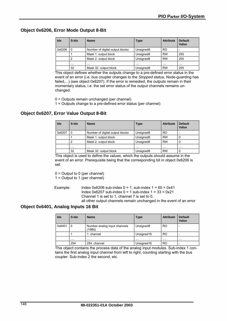
PIO Parker I/O-System
Object 0x6206, Error Mode Output 8-Bit
Idx S-Idx Name Type Attribute Default Value
0x6206 0 Number of digital output blocks Unsigned8 RO - 1 Mask 1. output block Unsigned8 RW 255 2 Mask 2. output block Unsigned8 RW 255 .... .... .... .... .... 32 Mask 32. output block Unsigned8 RW 255
This object defines wevent of an error (i.e.
hether the outputs change to a pre-defined error status in the bus coupler changes to the Stopped status, Node-guarding has
Object 0x6207,
failed,...) (see object 0x6207). If the error is remedied, the outputs remain in their momentary status, i.e. the set error status of the output channels remains un-changed.
0 = Outputs remain unchanged (per channel) 1 = Outputs change to a pre-defined error status (per channel)
Error Value Output 8-Bit
Idx S-Idx Name Type Attribute Default Value
0x6207 0 Number of digital output blocks Unsigned8 RO - 1 Mask 1. output block Unsigned8 RW 0 2 Mask 2. output block Unsigned8 RW 0 .... .... .... .... .... 32 Mask 32. output block Unsigned8 RW 0
This object is used to define the values, which the outputs should assume in the event of an error. Prerequisite being that the corresponding bit in object 0x6206 is set.
0 = Output to 0 (per channel) 1 = Output to 1 (per channel)
Example: Index 0x6206 sub-index 0 = 1, sub-index 1 = 65 = 0x41 Index 0x6207 sub-index 0 = 1 sub-index 1 = 33 = 0x21
or Channel 1 is set to 1, channel 7 is set to 0, all other output channels remain unchanged in the event of an err
Object 0x6401, Analog Inputs 16 Bit
Idx S-Idx Name Type Attribute Default Value
0x6401 0 Number analog input channels Unsigned8 RO - (16Bit)
1 1. channel Unsigned16 RO - .... .... .... .... .... 254 254. channel Unsigned16 RO -
This object contains the process data of the analog input modules. Sub-index 1 con-tains the first analog input channel from left to right, counting starting with the bus coupler. Sub-index 2 the second, etc.
88-022351-01A October 2003 146

EMN
Object 0x6411, Analog Outputs 16 Bit
Idx S-Idx Name Type Attribute Default Value
0x6411 0 Number analog input channels (16Bit)
Unsigned8 RO -
1 1. channel Unsigned16 RW 0 .... .... .... .... .... 254 254. channel Unsigned16 RW 0
This object contains the process data of s. Sub-index 1 con-tains the firs log o l frocoupler. Sub-index 2 the second, etc.
Object 0x6421, Analog Input Interrupt Trigger Selection
the analog output modulet ana utput channe m left to right, counting starting with the bus
Idx S-Idx Name Type Attribute Default Value
0x6421 0 Number analog input cha(16Bit)
ned8 RO - nnels Unsig
1 Trigger 1. channel Unsigned8 RW 7 .... .... .... .... .... Trigger 128. channel Unsigned8 RW 7 128
This object is used to define the condititransmission being that a 1 is entered in object 0x6423, and consequently the gen-er mi rele
Design Sub-Index 1..128:
on of the transmission. Prerequisite for the
al trans ssion ased.
Bit Transmission conditions Configuration Sub-Index
0 Threshold value exceeded 0x6424
1 Threshold value fallen short 0x6425
2 Change of the input value exceeding the delta value for st tr
0x6426 the la ansmission
3 Reduction of the input value by more than the delta 0x6427 value for the last transmission
4 Increase of the input value by more than the delta value for the last transmission
0x6428
5 to 7 Reserved -
Object 0x6423, Analog Input Global Interrupt Enable
Idx S-Idx Name Type Attribute Default Value
0x6423 0 Global Interrupt Enable A16Bit
0 nalog Unsigned8 RW
This obje t is used to control the transm ut data using PDO. If the is tran lea 421 and the t ansmission type of the PDO. I transmission of the analog inp is e, in je
c value
ission of the analog inp1, the smission is re sed, and it only depends on object 0x6
rut data
f the value is 0, no mad dependent of ob ct 0x6421.
88-022351-01A October 2003 147

PIO Parker I/O-System
Attention In t ault setting, the transmission of analog input data is deactivated. he def
Object 0x6424, peAnalog Input Interrupt Up r Limit Integer
Idx S-Idx Name Type Attribute Default Value
0x6424 0 Number analog input channels (16Bit)
Unsigned8 RO -
1 Upper Limit 1. channel Unsigned16 RW 0 .... .... .... .... .... 128 Upper Limit 128. channel Unsigned16 RW 0
This object allows a threshold value monitoring if it is configured in object 0x6423. If the input value is ≥ the defined threshold value, no transmission will take place until a further trigger condition is set (i.e. object 0x6426).
Transmission
Threshold value
Object 0x6425, Analog Input Interrupt Lower Limit Integer
Idx S-Idx Name Type Attribute Default Value
0x6425 0 Number analog input channels (16Bit)
Unsigned8 RO -
1 Lower Limit 1. channel Unsigned16 RW 0 .... .... .... .... .... 128 Lower Limit 128. channel Unsigned16 RW 0
This object allows a threshold value monitoring if it is configured in object 0x6423. If the input value is ≤ the determined threshold value, transmission will take place until a further trigger condition is set (i.e. object 0x6426).
Transmission
Threshold value
88-022351-01A October 2003 148

EMN
Object 0x6426, Analog Input Interrupt Delta Unsigned
Idx S-Idx Name Type Attribute Default Value
0x6426 0 Number analog input channels (16Bit)
Unsigned8 RO -
1 Delta value 1. channel Unsigned16 RW 0 .... .... .... .... .... 128 Delta value 128. channel Unsigned16 RW 0
The new value to be transmitted must, by definition of this object, be larger by at least the delta value or smaller than the value sent before.
This object, for instance, can be linked with the object 0x6424, so that the transmis-sion will only be completed when the set threshold value and also the delta function are fulfilled.
Delta
Delta
Transmission
Transmission
Object 0x6427, Analog Input Inte
Previous value
rrupt Negative Delta Unsigned
Idx S-Idx Name Type Attribute Default Value
0x6427 0 Number analog input channels (16Bit)
Unsigned8 RO -
1 Delta value 1. channel Unsigned16 RW 0 .... .... .... .... .... 128 Delta value 128. channel Unsigned16 RW 0
By definition of this object, the new value to be transmitted, must be smaller than the previously sent value, at least by the delta value.
DeltaPrevious value
Transmission
88-022351-01A October 2003 149

PIO Parker I/O-System
Object 0x6428, Analog Input Interrupt Positive Delta Unsigned
Idx S-Idx Name Type Attribute Default Value
0x6428 0 Number analog input channels (16Bit)
Unsigned8 RO -
1 Delta value 1. channel Unsigned16 RW 0 .... .... .... .... .... 128 Delta value 128. channel Unsigned16 RW 0
By definition of this object, the new value to be transmitted, must be larger than the previously sent value, at least by the delta value.
Delta
Tra
Previous value
nsmission
Object 0x6443,
Analog Output Error Mode
Idx S-Idx Name Type Attribute Default Value
0x6443 0 Number analog output channels (16Bit)
Unsigned8 RO -
1 Error Mode 1. channel Unsigned8 RW 1 .... .... .... .... .... 128 Error Mode 128. channel Unsigned8 RW 1
This(see
object is used to define whether the outputs change to a pre-defined error status object 0x6444) in the event of an error (i.e. bus coupler changes to the Stopped
Object 0x6444,
status, Nodeguarding has failed,...). Once the error is remedied, the outputs retain their momentary status, i, e. the set error status of the output channels remains un-changed.
All analog outputs that are not covered by the object 0x6444 (i.e. analog 6 byte mod-ules) are always set to 0 in the event of an error.
0 = The output remains unchanged 1 = The output changes to a pre-defined error status
Analog Output Error Value Integer
Idx S-Idx Name Type Attribute Default Value
0x6444 0 Number analog output channels (16Bit)
Unsigned8 RO -
1 Error value 1. channel Unsigned16 RW 0 .... .... .... .... .... 128 Error value 128. channel Unsigned16 RW 0
This object is used to define values that they are to assume in the event of an error. Prerequisite being that the corresponding bit is set in object 0x6443.
88-022351-01A October 2003 150
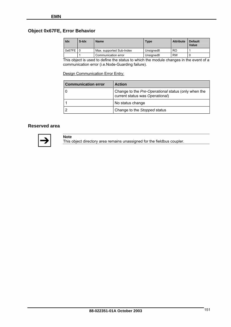
EMN
Object 0x67FE, Error Behavior
Idx S-Idx Name Type Attribute Default Value
0x67FE 0 Max. supported Sub-Index Unsigned8 RO 1 1 Communication error Unsigned8 RW 0
This object is used to define the status to which the module changes in the event of a
Des
communication error (i.e.Node-Guarding failure).
ign Communication Error Entry:
Communication error Action
0 Change to the Pre-Operationacurrent status was Operation
l status (only when the al)
1 No status change
2 Change to the Stopped status
Reserved area
Note This object directory area remains unassigned for the fieldbus coupler.
88-022351-01A October 2003 151
PIO Parker I/O-System
5.3.5 PDO Transmission
When changing to the Operational status, all TxPDOs are transmitted once with the t ission
Data transmission with PDOs is only possible in the Operational status.
ransm type 254 and 255.
Note S al transm sion type ( 0x1800 .. 0x181F, The analog changes are not transmitted because of the default value (=FALSE) ac-cording to the device profile DS401-ObjeE le). In th anner, a o p nt an ov low when ong Inhibit Time can be selected. Moreover, there iso ssages configurin s 0 1, 0x64 0x6425) 6, 0x6427, 0x6428).
peciIndex
is .
254 and 255 sub-index 2):
ct 0x6423 (analog Input Global Interrupt CAN bus overflow with CAN messages is prevented. Tnab is m
reve erf setting the object 0x6423 = TRUE, a correspondingly l the possibility to reduce the amount
g the objects for the threshold value monitoring (objectf me by x642 24, and for the delta functions (objects 0x642
Mapping
can define the data to be transmitted by means of PDOs.
a
By PDO mapping you
If no stored customer specific configuration is used and if no other settings are per-formed, the object directory is assigned with a default configuration according to the device profile DS 401 (refer to chapter “Initialization”).
If the coupler is in the PRE-OPERATIONAL status, its mapping can be modified viSDOs instead, in an application specific manner.
i
Further information Ft
or an example of how to create an application specific mapping configuration, refer o chapters 3.1.6, "Start-up".
88-022351-01A October 2003 152
EMN
5.3.6 SYNC M
If the value of the communication cycle period is unequal to 0, monitoring is made with the first arrival of a SYNC message if the bus coupler is in the Operational status.
Failure of SY ag
onitoring
NC mess e:
If no SYNC message is received within the monitoring time (communication cycle pe-riod), this is signalled by a blink code. No status change occurs. In addition, an emer-gency message (Error Code: 0x8100, Error Register: 0x81, Additional Code: 00 04 00 00 00) is sent. The failure of the SYNC message will be displayed even if the MASTER provokes a status change.
OPERATIONAL tatus that the LEDs regain their normal operating status, and another emergency
er: 0x81, Additional Code: 00 04 00 000 C monitoring functions again.
5.3.7 Node Gu
The Node Guarding starts for the bus coupler when the first remote transmit request message (RTR) is received on the COB ID for the Node Guarding (0x700+Module-I bus ives no in de ot monitored by the bus coupler.
In the default setting, the Node Guarding is deactivated, because a 0 is entered in the c nding 100C = e,
T mas bus cou ula rvaGuard-Time (Index 0x100C). The internal status of the bus coupler is in the reply message.
On the arrival of an RTR request without the Guard Time being set, the Node Guard-i t mon s p ts inter
The status is coded as follows:
It is only after the repeated receipt of the SYNC message in the smessage (Error Code: 0x0000, Error Regist0) is sent to show that the SYN
arding
D). If the coupler rece correspond g message, the No Guarding is n
orrespo indexes (0x Guard-Tim 0x100D = Life Time Factor).
he NMT ter polls the pler at reg r intervals. This inte l is termed
ng is no itored, nevertheles the bus cou ler replies with i nal status.
State: Value:
PRE-OPERATIONAL 127
OPERATIONAL 5
STOP 4
Life-Time is the product of Guard-Time (Index 0x100C) and Life Time Factor (Index 0x100D).
Failure of Node Guarding:
If no Node Guarding message is received with the life-time, this is shown by a blink code. In addition, an emergency message (Error Code: 0x8130, Error Register: 0x11,
7FE.
Additional Code: 0x00 04 00 000 0) is sent, the outputs are activated according to the objects 0x6206, 0x6207, 0x6443 and 0x6444, and the bus coupler changes to the pre-defined status according to object 0x6
88-022351-01A October 2003 153

PIO Parker I/O-System
As soon as the Node Guarding protocol is recorded, another emergency message (Error Code: 0x0000, Error Register: 0x11, Additional Code: 00 04 00 000 0) is sent to show that the Node Guarding is reactivated, whereby the outputs and the bus cou-pler status remain unchanged.
the Heartbeat protocol. If the Heartbeat-Producer-Time is configured, t
5.3.8 Heartbeat
ithout having to use RTR frames.
The Heartbeat generator cyclically generates a message (time interval defined in ob-
ing the object 0x1017. The message can be evaluated by one or several Heartbeat consumers (object 0x1016). A maximum of 5 modules can be
itored. Monitoring starts with the first arrival of a Heartbeat message (separate
It is possible to only use the Node Guarding protocol or he Heartbeat protocol is always used.
Monitoring
This protocol allows for monitoring the modules w
ject 0x1017), in which it transmits the module status. Transmission begins immedi-ately after configur
monfor every module to be monitored).
Failure of the Heartbeat:
If no corresponding Heartbeat message is received within the configured time (object0x1016), this is signalled by a blink code. In addition, an emergency message (Error
30, Error Register: 0x11, Additional Code: 0x00 05 KK 00 00, KK node number which has triggered EMCY) is sent. The outputs are activated according to objects 0x6206, 0x6207, 0x6443 and 0x6444 and the bus coupler changes to the status pre-defined according to 0x67FE.
As soon as the Heartbeat protocol is recorded, another emergency message (Error ode: 0x0000, Error Register: 0x11, Additional Code: 0x00 05 KK 00 00) is sent to
display that Heartbeat is active again, whereby the outputs and the bus coupler eral modules are monitored, the blink code signalling stops after the previous Heartbeat has been re-
sumed.
The only protocols to be used are the Node Guarding or the Heartbeat protocol. The Heartbeat protocol is used whenever the Heartbeat producer time is configured.
5.3.9 Error Message (Emergency)
Emergency messages are alway a critical error situation having occurred/overcome in the device tion has to be communicated to other devices.
Structure and meaning of the ent ency object are explained in the ta-ble “EMCY-CODE”, they are cod ssage in a Lowbyte / Highbyte or-der.
An emergency object is also sent, after an error is remedied (Error Code = 0x0000, the Error Register and the Additional Code behave as described in the table “EMCY-CODE”).
Following Power On an emergency object is sent if the loaded settings are the default settings. This occurs for two reasons:
• No settings have yet been saved (Index 0x1010).
Code: 0x81
C
status remain unchanged. If sevthe failure of the Heartbeat only
s sent in the event of , or if important informa
ries in the emerged in the bus me
88-022351-01A October 2003 154

EMN
• The saved settingconnected or dis
were discarded by the bus coupler, because modules were connected.
EMCY-CODE Byte: 0 1 2 3 7
Name Error Code
Error Register
Additional Code Meaning
0x0000* 0x00 00 00 00 00 00 The "predefined SubIdx. 0 set to zero or all errors are cleared
error field" Index 0x1003
0x5000* 0x81 00 01 00 00 00 Changed hardw er on or reset Node / communication The fieldbus coupler is be initialized, because no stored configuration is able does not coincide with the current configuration
are configuration after pow
available or the one avail
0x5000* 0x81 00 02 00 00 00 Flash errors An error has occurred wFlash.
hen saving the configuration in
0x5000* 0x81 00 03 PP LL SS The programme coincide with the actual one PP: physical mo has occurred LL: logic module slot wSS: Cause of th
d configuration does not
dule slot where the errorhere the error has occurred
e error 0x5000* 0x81 00 09 00 00 00 Queue overflow s
(can only occur w is used)
for emergency messagehen the inhibit time for emergency
0x8100* 0x81 00 04 00 00 00 The time span b is longer than the communica
etween two SyncObjectstion_Cycle_Period
0x8110* 0x11 00 01 00 00 00 internal receivestatus change as defined in are switched as defined in the Error-Mode/Value Ob-jects
buffer overflow, object 0x67FE. The outputs
0x8110* 0x11 00 02 00 00 00 internal transmit buffer overflow, status change as defined in object 0x67FE. The outputs are switched as defined in the Error-Mode/Value objects
CAN Controller in Error Passive Mode 0x8120* 0x11 00 03 00 00 00 0x8130 The time between two node guarding telegrams is
greater than Guard_Time * Life_Time_Faktor. * 0x11 00 04 00 00 00
0x8130* 0x11 00 05 KK 00 00 The time between two Heartbeat telegrams is greater than configured KK: Node that has tripped the time overflow
0x8210* 0x81 00 05 SS II NN PDO was sent with a number of bytes smaller than that in the communication profile.
scarded, i.e. the outputs remain unchanged SS:Set point value - configured value (i.e. in Index 0x1600 Sub-index 0) II:Actual value - number of bytes sent NN:Number of PDO (1..32)
configuredThe PDO data is di
0x8220* 0x81 00 08 SS II NN PDO was sent with a number of bytes larger than that configured in the communication profile. Only the first n data is used (n = total length configured in the object directory) SS:Set point value - configured value (total length of all valid and configured objects in bytes) II:Actual value - number of bytes sent NN:Number of PDO (1..32)
0xFF00* 0x81 00 06 PP 00 00 Module bus error, change to the STOP status - PP: Module position
0xFF00* 0x81 DD 07 PP SK NN Diagnosis message - DD: Diagnosis byte - PP: Module position - SK:Error status and channel number - NN :Number of current module error
88-022351-01A October 2003 155

PIO Parker I/O-System
Byte: 0 1 2 3 7
Name Error Code
Error Register
Additional Code Meaning
* Byte 0 = Lowbyte and Byte 1 = Highbyte Example: Error Code 0x8220: Byte 0 = 0x20, Byte 1= 0x82
Diagnostic message of I/O modules
In the event of an error occurring in a module, which supports diagnostics, the diag-nostic status is transmitted by means of the emergency message.
DD 07 PK SK NN
Design of the Additional Code of the Diagnosis message:
Number of current module errors
Bit 0,1 indicates the channel number of the module (channel 0..3)
Bit 2..7 reserved
Bit 8 indicates detected or cleared errors
Bit 8 = 1 Error detected, Bit 8 = 0 Error cleared
Position of the module
Identifier of the diagnosis message
Module specific diagnosis byte (analog modules)
Module specific diagnosis byte (digital modules)
0 if the error have been cleared, i.e. byte SK Bit 8 = 0 Fig. 5-1: Design of Additional Code
Example:
• 2 channel analog input module, connected at position14, current on channel 0 has more than 20mA.
00 FF 81 42 07 0E 80 01
Emergency Telegram
1 Error
Channel 0
Error detected
Module plugged at position 14
Diagnosis message
Current > 20,5 mA (see module description)
Error Register
Error Code Fig. 5-2: Design Emergency Message 1
88-022351-01A October 2003 156
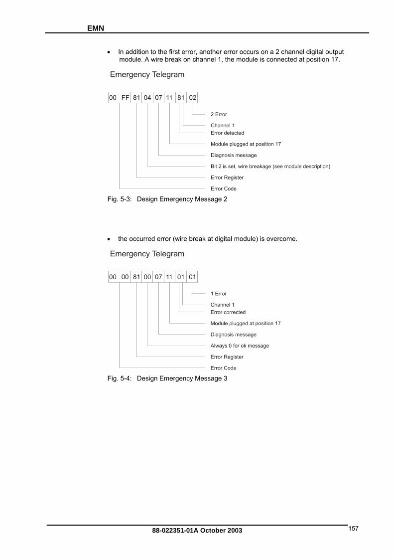
EMN
• In addition to the first errmodule. A wire break on
or, another error occurs on a 2 channel digital output channel 1, the module is connected at position 17.
00 FF 81 04 07 11 81 02
Emergency Telegram
2 Error
Channel 1
Error detected
Module plugged at position 17
Diagnosis message
Error Register
Fig. 5-3:
the occurred error (wire break at digital module) is overcome.
Bit 2 is set, wire breakage (see module description)
Error Code Design Emergency Message 2
•
00 00 81 00 07 11 01 01
1 Error
Em
Module plugged at position 17
Fig.
ergency Telegram
Channel 1
Error corrected
Diagnosis message
Always 0 for ok message
Error Register
Error Code 5-4: Design Emergency Message 3
88-022351-01A October 2003 157

PIO Parker I/O-System
6 zardous Environments 6.1 Foreword
use gas-air, vapor-air and ectrical components u
law, directives or regulations on a national and international scale. The I/O-SYSTEM (electrical components) is d
6.2 Protective measures Primarily, explosion protection describes how to prevent the formation of an explosive
concentration levels, ventilnumber of applications, which do not allow the implementation of primary protection measures. In such cases, the secondary explosion protection comes into play. Fol-
6.3 Classification meeting CENELEC and IEC The specifications outlined here are valid for use in Europe and are based on the fol-
standards of the IEC (I
Use in Ha
Today’s development shows that many chemical and petrochemical companies have production plants, production, and process automation machines in operation which
dust-air mixtures which can be explosive. For this reason, the el sed in such plants and I/O-systems must not pose a riskof explosion resulting in injury to persons or damage to property. This is backed by
esigned for use in zone 2 explosive environments. The following basic explosion protection related terms have been defined.
atmosphere. For instance by avoiding the use of combustible liquids, reducing the ation measures, to name but a few. But there are a large
lowing is a detailed description of such secondary measures.
lowing standards: EN50... of CENELEC (European Committee for Electrotechnical Standardization). On an international scale, these are reflected by the IEC 60079-...
nternational Electrotechnical Commission).
6.3.1 Divisions
e e. The term explos exist-
ing in the form of air-borne tmospheric conditions which, when heated beyond a tolerable temperatursparks, can produce explosions. Explosive zones have been created to describe the concentrations level of an explosive atmosphere. This division, based on the probability of an explosion occurring, is of great importance both for technical safety and feasibility reasons. Knowing that the demands placed on electrical components permanently employed in an explosive environment have to be much more stringent than those placed on electrical components that are only rarely and, if at all, for short periods, subject to a dangerous explosive environment.
Explosive environments are areas in which the atmosphere can potentially becomexplosiv ive means a special mixture of ignitable substances
gases, fumes, mist or dust under ae or subjected to an electric arc or
88-022351-01A October 2003 158

EMN
Explosive areas resulting from gases, fumes or mist:
• Zone 0 areas are subject to an explosive atmosphere ntinuously or for extended periods.
as can expect the occasional occurrence of an explosive atmosphere ≤ 1000 h /year).
• Zone 2 areas can expect the rare or short-term occurrence of an explosive atmosphere (> 0 h ≤ 10 h /year).
Explosive areas subject to air-borne dust:
• Zone 20 areas are subject to an explosive atmosphere (> 1000 h /year) continuously or for extended periods.
• Zone 21 areas can expect the occasional occurrence of an explosive atmosphere (> 10 h ≤ 1000 h /year).
• Zone 22 areas can expect the rare or short-term occurrence of an explosive atmosphere (> 0 h ≤ 10 h /year).
6.3.2 Explosion protection group
In addition, the electrical components for explosive areas are subdivided into two groups:
Group I: Group I includes electrical components for use in fire-damp en-dangered mine structures.
Group II: Group II includes electrical components for use in all other explo-sive environments. This group is further subdivided by pertinent combustible gases in the environment. Subdivision IIA, IIB and IIC takes into account that different mate-rials/substances/gases have various ignition energy characteris-tic values. For this reason the three sub-groups are assigned representative types of gases: • IIA – Propane • IIB – Ethylene • IIC – Hydrogen
(> 1000 h /year) co
• Zone 1 are(> 10 h
Minimal ignition energy of representative types of gases
Explosion group I IIA IIB IIC
Gases Methane Propane Ethylene Hydrogen
Ignition energy (µJ) 280 250 82 16 Hydrogen being commonly encountered in chemical plants, frequently the explosion group IIC is requested for maximum safety.
88-022351-01A October 2003 159

PIO Parker I/O-System
6.3.3 Unit categories
Moreover, the areas of use (zones) and the conditions of use (explosion groups) are subdivided into categories for the electrical operating means:
Unit catego-ries
Explosion group
Area of use
M1 I Fire-damp protection
M2 I Fire-damp protection
1G II Zone 0 Explosive environment by gas, fumes or mist
2G II Zone 1 Explosive environment by gas, fumes or mist
3G II Zone 2 Explosive environment by gas, fumes or mist
1D II Zone 20 Explosive environment by dust
2D II Zone 21 Explosive environment by dust
3D II Zone 22 Explosive environment by dust
erature classes
The maximum surface temperature for electrical components of explosion protection ue to coal dust deposits) or 450 °C (if there is no danger
rface temperature for all ignition protection types, the bdivided into temperature classes, as far as electrical
protection group II are concerned. Here the temperatures perature of 40 °C for operation and testing of the electrical
e of the existing explosive atmosphere ust be higher than the maximum surface temperature.
6.3.4 Temp
group I is 150 °C (danger dof coal dust deposit).
In line with the maximum su suelectrical components are
components of explosion refer to a surrounding temcomponents. The lowest ignition temperaturm
Temperature classes
Maximum surface temperature
Ignition temperature of the combustible materials
T1 450 °C > 450 °C
T2 300 °C > 300 °C to 450 °C
T3 200 °C > 200 °C to 300 °C
T4 135 °C > 135 °C to 200 °C
T5 100 °C >100 °C to 135 °C
T6 85°C > 85 °C to 100 °C
88-022351-01A October 2003 160

EMN
88-022351-01A October 2003 161
The following table represents the division and attributes of the materials to the tem-perature classes and material groups in percent:
Temperature classes T1 T2 T3 T4 T5 T6 TotalP
*P
26.6 % 42.8 % 25.5 %
94.9 % 4.9 % 0 % 0.2 % 432
Explosion group IIA IIB IIC TotalP
*P
85.2% 13.8 % 1,0 % 501 P
*P Number of classified materials
6.3.5 Types of ignition protection
Ignition protection defines the special measures to be taken for electrical components in order to prevent the ignition of surrounding explosive atmospheres. For this reason a differentiation is made between the following types of ignition protection:
Identifi-cation
CENELEC stan-dard
IEC stan-dard
Explanation Application
EEx o EN 50 015 IEC 79-6 Oil encapsulation Zone 1 + 2
EEx p EN 50 016 IEC 79-2 Overpressure en-capsulation
Zone 1 + 2
EEx q EN 50 017 IEC 79-5 Sand encapsulation Zone 1 + 2
EEx d EN 50 018 IEC 79-1 Pressure resistant encapsulation
Zone 1 + 2
EEx e EN 50 019 IEC 79-7 Increased safety Zone 1 + 2
EEx m EN 50 028 IEC 79-18 Cast encapsulation Zone 1 + 2
EEx i EN 50 020 (unit) EN 50 039 (sys-tem)
IEC 79-11 Intrinsic safety Zone 0 + 1 + 2
EEx n EN 50 021 IEC 79-15 Electrical compo-nents for zone 2 (see below)
Zone 2
Ignition protection “n" describes exclusively the use of explosion protected electrical components in zone 2. This zone encompasses areas where explosive atmospheres can only be expected to occur rarely or short-term. It represents the transition be-tween the area of zone 1, which requires an explosion protection and safe area in which for instance welding is allowed at any time.
Regulations covering these electrical components are being prepared on a world-wide scale. The standard EN 50 021 allows electrical component manufacturers to obtain certificates from the corresponding authorities for instance KEMA in the Neth-erlands or the PTB in Germany, certifying that the tested components meet the above mentioned standards draft.
Type “n” ignition protection additionally requires electrical components to be marked with the following extended identification:

PIO Parker I/O-System
88-022351-01A October 2003 162
• A – non spark generating (function modules without relay /without switches)
• AC – spark generating, contacts protected by seals (function modules with relays / without switches)
• L – limited energy (function modules with switch)
i
Further information For more detailed information please refer to the national and/or international stan-dards, directives and regulations!
6.4 Classifications meeting the NEC 500 The following classifications according to NEC 500 ( UN Uational UEUlectric UC Uode) are valid for North America.
6.4.1 Divisions
The "Divisions" describe the degree of probability of whatever type of dangerous situation occurring. Here the following assignments apply:
Explosion endangered areas due to combustible gases, fumes, mist and dust:
Division 1 Encompasses areas in which explosive atmospheres are to be ex-pected occasionally (> 10 h ≤ 1000 h /year) as well as continuously and long-term (> 1000 h /year).
Division 2 Encompasses areas in which explosive atmospheres can be ex-pected rarely and short-term (>0 h ≤ 10 h /year).
6.4.2 Explosion protection groups
Electrical components for explosion endangered areas are subdivided in three dan-ger categories: Class I (gases and fumes): Group A (Acetylene)
Group B (Hydrogen) Group C (Ethylene) Group D (Methane)
Class II (dust): Group E (Metal dust) Group F (Coal dust) Group G (Flour, starch and cereal dust)
Class III (fibers): No sub-groups
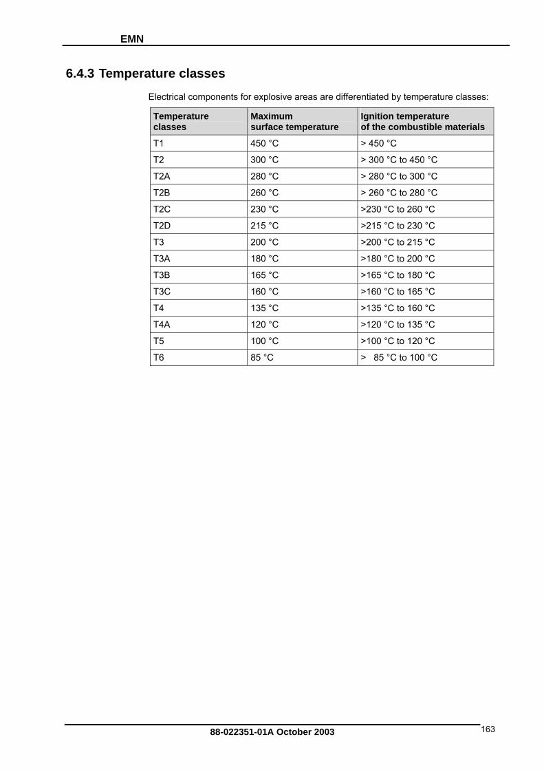
EMN
88-022351-01A October 2003 163
6.4.3 Temperature classes
Electrical components for explosive areas are differentiated by temperature classes:
Temperature classes
Maximum surface temperature
Ignition temperature of the combustible materials
T1 450 °C > 450 °C
T2 300 °C > 300 °C to 450 °C
T2A 280 °C > 280 °C to 300 °C
T2B 260 °C > 260 °C to 280 °C
T2C 230 °C >230 °C to 260 °C
T2D 215 °C >215 °C to 230 °C
T3 200 °C >200 °C to 215 °C
T3A 180 °C >180 °C to 200 °C
T3B 165 °C >165 °C to 180 °C
T3C 160 °C >160 °C to 165 °C
T4 135 °C >135 °C to 160 °C
T4A 120 °C >120 °C to 135 °C
T5 100 °C >100 °C to 120 °C
T6 85 °C > 85 °C to 100 °C

PIO Parker I/O-System
88-022351-01A October 2003 164
6.5 Identification
6.5.1 For Europe
According to CENELEC and IEC
II 3 GKEMA 01ATEX1024 X
EEx nA II T4
Explosion protection group Unit category
Community symbol forexplosion protectedelectrical components
Approval body and/or number ofthe examination certificate
E = conforming with European standardsEx = explosion protected component
n = Type of ignition Extended identification
Explosion protection group
Temperature class
Fig. 6-1: Example for lateral labeling of bus modules (PIO-400, 2 channel digital input module 24 V DC)

EMN
88-022351-01A October 2003 165
6.5.2 For America
According to NEC 500
CL I DIV 2Grp. ABCD
optemp code T4AExplosion group(gas group)
Explosion protection group(condition of use category)
Area of application (zone)
Temperature class
Fig. 6-2: Example for lateral labeling of bus modules (PIO-400, 2 channel digital input module 24 V DC)

PIO Parker I/O-System
88-022351-01A October 2003 166
6.6 Installation regulations In the Federal Republic of Germany, various national regulations for the installation in explosive areas must be taken into consideration. The basis being the ElexV com-plemented by the installation regulation DIN VDE 0165/2.91. The following are ex-cerpts from additional VDE regulations:
DIN VDE 0100 Installation in power plants with rated voltages up to 1000 V DIN VDE 0101 Installation in power plants with rated voltages above 1 kV DIN VDE 0800 Installation and operation in telecommunication plants includ-
ing information processing equipment DIN VDE 0185 lightning protection I/O-systems
The USA and Canada have their own regulations. The following are excerpts from these regulations:
NFPA 70 National Electrical Code Art. 500 Hazardous Locations ANSI/ISA-RP 12.6-1987 Recommended Practice C22.1 Canadian Electrical Code
• Danger When using the I/O-SYSTEM (electrical operation) with Ex approval, the follow-ing points are mandatory:
A. The fieldbus independent I/O-system Modules Type PIO-xxx are to be installed in enclosures that provide for the degree of ingress protection of at least IP54. For use in the presence of combustible dust, the above mentioned modules are to be installed in enclosures that provide for the degree of ingress protection of at least IP64.
B. The fieldbus independent I/O-system may only be installed in hazardous areas (Europe: Group II, Zone 2 or America: Class I, Division 2, Group A, B, C, D) or in non-hazardous areas!
C. Installation, connection, addition, removal or replacement of modules, fieldbus connectors or fuses may only take place when the I/O-system supply and the field supply are switched off, or when the area is known to be non-hazardous.
D. Ensure that only approved modules of the electrical operating type will be used. The Substitution or Replacement of modules can jeopardize the suitability of the I/O-system in hazardous environments!
E. Operation of intrinsically safe EEx i modules with direct connection to sen-sors/actuators in hazardous areas of Zone 0 + 1 and Division 1 type requires the use of a 24 V DC Power Supply EEx i module!
F. DIP switches and potentiometers are only to be adjusted when the area is know to be non-hazardous.
i
Further Information Proof of certification is available on request. Also take note of the information given on the module technical information sheet.

EMN
88-022351-01A October 2003 167
7 Glossary TBit T Smallest information unit. Its value can either be 1 or 0.
TBitrate T Number of bits transmitted within a time unit.
TBootstrap T Operating mode of the fieldbus coupler. Device expects a firmware upload.
TBus T A structure used to transmit data. There are two types, se-rial and parallel. A serial bus transmits data bit by bit, whereas a parallel bus transmits many bits at one time.
TByte T Binary Yoked Transfer Element. A byte generally contains 8 bits.
TData bus T see Bus.
TFieldbusT I/O-system for serial information transmission between devices of automation technology in the process-related field area.
THardware T Electronic, electrical and mechanic components of a module/subassembly.
Operating I/O-system Software which links the application programs to the hardware.
TSegment T Typically, a network is divided up into different physical network segments by way of routers or repeaters.
TServerT Device providing services within a client/server I/O-system. The service is requested by the Client.
TSubnet T A portion of a network that shares the same network ad-dress as the other portions. These subnets are distin-guished through the subnet mask.

PIO Parker I/O-System
88-022351-01A October 2003 168
8 Literature list
i
Further information CAN in Automation (CiA) provides further documentation for its members in INTERNET. HTUcan-cia.de UTH

EMN
88-022351-01A October 2003 169
9 Index
C carrier rail · 17, 20 Contact
Carrier rail · 101 contacts
data- · 21 power- · 27
D data contacts · 21
E Electrical isolation · 36
F Fieldbus node · 49, 101, 102 Fieldbus nodes · 100
I Internal bus · 34
L Light diodes · 37 locking disc · 19
P PIO-400 [2 DI DC 24 V 3.0 ms, High-Side Switching] · 59 PIO-402 [4 DI DC 24 V 3.0 ms, High-Side Switching] · 62 PIO-430 [8 DI DC 24 V 3.0 ms, High-Side Switching] · 65 PIO-468 [4 AI DC 0-10 V, Single-Ended] · 68 PIO-480 [2 AI 0-20 mA Differential Measurement Input] · 72 PIO-501 [2 DO DC 24V 0.5 A, High-Side Switching] · 77 PIO-504 [4 DO DC 24 V 0.5 A, High-Side Switching] · 80 PIO-530 [8 DO DC 24 V 0.5 A, High-Side Switching] · 83 PIO-550 [2 AO DC 0-10 V] · 86 PIO-552 [2 AO 0-20 mA] · 90 PIO-600 [End Module] · 94 PIO-602 [24 V DC Power Supply] · 96 Power contacts · 22, 27
not carried out · 27 Process image · 48
S Start-up · 99 Subnet · 167
U unlocking lug · 19