hard x-ray photoemission spectroscopy
TRANSCRIPT

ARTICLE IN PRESS
Nuclear Instruments and Methods in Physics Research A 601 (2009) 32–47
Contents lists available at ScienceDirect
Nuclear Instruments and Methods inPhysics Research A
0168-90
doi:10.1
E-m
journal homepage: www.elsevier.com/locate/nima
Hard X-ray photoemission spectroscopy
Keisuke Kobayashi
NIMS Beamline Station at SPring-8, National Institute for Materials Science, 1-1-1 Kouto, Sayo-cho, Sayo-gun, Hyogo 619-5198, Japan
a r t i c l e i n f o
Available online 6 January 2009
Keywords:
Hard X-ray photoemission
Electronic structure
Chemical bonding state
Undulator X-rays
02/$ - see front matter & 2008 Elsevier B.V. A
016/j.nima.2008.12.188
ail address: [email protected]
a b s t r a c t
Except in the very early stage of the development of X-ray photoemission spectroscopy (XPS) by Kai
Siegbahn and his coworkers, the excitation sources for XPS studies have predominantly been the Al Kaand Mg Ka emission lines. The advent of synchrotron radiation sources opened up the possibility of
tuning the excitation photon energy with much higher throughputs for photoemission spectroscopy,
however the excitation energy range was limited to the vacuum ultra violet and soft X-ray regions.
Over the past 5–6 years, bulk-sensitive hard X-ray photoemission spectroscopy using high-brilliance
high-flux X-rays from third generation synchrotron radiation facilities has been developed. This article
reviews the history of HXPES covering the period from Kai Siegbahn and his coworkers’ pioneering
works to the present, and describes the fundamental aspects, instrumentation, applications to solid
state physics, applied physics, materials science, and industrial applications of HXPES. Finally, several
challenging new developments which have been conducted at SPring-8 by collaborations among several
groups are introduced.
& 2008 Elsevier B.V. All rights reserved.
1. Introduction
Since the pioneering works of Kai Siegbahn and his co-workers[1,2], X-ray photoemission spectroscopy has grown to be one ofthe most universal and powerful tools available for the investiga-tion of chemical states and electronic structures of materials.Today it is widely used in laboratories and factories for scientificinvestigations as well as for industrial purposes such as failureanalysis and product-line monitoring. This is due to the develop-ment of commercially available sophisticated hardware using AlKa and Mg Ka excitation sources and sophisticated analysissoftware. The use of synchrotron radiation introduces the abilityto tune the excitation photon energy over a wide range, and third-generation synchrotron radiation facilities offer opportunities forhigh-resolution, high-throughput photoemission spectroscopy.However, the use of synchrotron radiation was for a long timelimited to the VUV/SX energy region. The probing depth ofphotoemission spectroscopy was thus limited to be less than afew nm, and surface sensitivity, good or bad, was one of thecharacteristics of the method. The first report of high-resolutionhard X-ray photoemission experiments (HXPES) using a third-generation undulator X-ray source was published in 2003 [3].(In this article, I use the abbreviation HXPES, but in the literaturethere are many other forms, including HX-PES, HXPES, HEPES,HAXPES and HIKE. The abbreviation HXPES ties in well withSXPES, the commonly used abbreviation for soft X-ray photo-
ll rights reserved.
emission spectroscopy.) Several groups began HXPES activities inJapan as well as in Europe at almost the same time. In this article,I would like to describe the evolution of the utilization andtechnical aspects of HXPES following the ‘‘1st InternationalWorkshop on HAXPES’’ held at the ESRF in Grenoble, France fromSeptember 11–12, 2003. The purpose of this article is to offer anoverview of HXPES activities and present the potential of thispromising and versatile method for those who are not yetinvolved, but have an interest.
2. Historical of HXPES development
Kai Siegbahn and co-workers are credited with the first hardX-ray photoemission experiments [2]. Successful examples of Mg1s, Mg 2p, and O 1s core spectra were reported using Cu Ka and CuKb radiation. As the Cr Kb and Cu Kb wavelengths are very close to1/4 and 1/6 of the Al Ka wavelength, respectively, Al/Cr or Al/Cudouble X-ray sources using bent quartz crystals to monochroma-tize and focus the X-rays were developed (for example, SCIENTAESCA300). However, due to insufficient intensity of the Cu Kbexcitation, these sources have not been widely used for practicalapplications.
The first high resolution hard X-ray photoemission spectro-scopy experiments using synchrotron radiation were performedby Lindau et al. in 1974 [4], who used X-rays from a bendingmagnet at SPEAR (Stanford Synchrotron Radiation Laboratory) tomeasure the intrinsic linewidth of the Au 4f core levels with highenergy resolution. The observed peak count rate was very low,

ARTICLE IN PRESS
(arb
. uni
ts) Si-SiSi-O
Si 1sTOA=80ºHard X-ray
hν= 7935 eV
Photoelectrons
K. Kobayashi / Nuclear Instruments and Methods in Physics Research A 601 (2009) 32–47 33
thus no further trials aiming at high resolution hard X-rayspectroscopy for practical studies were attempted until the firstreport of HXPES using undulator X-rays in 2003. Meanwhile,double crystal monochromators at bending magnet beamlinescontinued to be used for high energy photoemission spectroscopywith medium resolution for Auger and XPS studies [5–14]. Adedicated high energy XPS instrument was installed at a HASYLAB wiggler beamline in 1993 [15]. Combination of X-ray standingwave techniques with high energy PES were also tried by severalgroups [6,16,17].
Breakthroughs in the HXPES technique were made by severalgroups at the ESRF and also at SPring-8 independently in2002–2004 [3,18–22,26]. At SPring-8, a JASRI-RIKEN collaborationsucceeded in the first feasibility test using 6 keV X-ray excitationin 2002 at the RIKEN beamline BL29XU. In this collaboration,various user groups in the fields of Si-LSI, compound semicon-ductors, and spin electronics researches were involved fromthe beginning [3,18]. Collaboration with Hiroshima UniversitySynchrotron Radiation Research Center (HiSOR) has also beenincluded from the very early stages. At the ESRF, activities at ID32had already begun [21], and HXPES instrumentation was installedin the VOLPE project at ID16 [20] at almost the same time.
One of the most essential factors for the breakthrough inHXPES is the use of high brilliance undulator X-rays. Theundulators at 3rd generation synchrotron radiation facilitiessuch as the ESRF and SPring-8 provide photon fluxes of higherthan 1011 photons/sec even after the reduction of bandwidthsdown to around 50 meV or less. The reduction of the bandwidthsis realized by a channel-cut Si single crystal post monochromator,which is installed downstream of the beamline monochromator.Another improvement was the development of hardware forhigh kinetic energy electron analysis [20–26]. A total resolution of60 meV has been achieved at 8 keV [27], but for practical purposesa total resolution of 200–250 meV is used. Channel-cut post-monochromators and high voltage analyzers have also success-fully introduced to bending magnet beamlines at the ESRF [25],and BESSY II [28], where sufficient X-ray fluxes are available forcore level spectroscopy.
At SPring-8, HXPES R&D activities at BL47XU were began bythe JASRI group in 2004. HXPES beamtime was partially openedfor public use in the latter half of 2004, and the number ofaccepted proposals grew rapidly [29]. Because of the rapidincrease in demand from industrial users, part of the beamtimeat BL39XU was devoted to these studies. These industrial subjectshave recently been transferred to BL46XU, where an experimentalstation exclusively for HXPES has been constructed. Meanwhile, agroup from Osaka University began activities at the 20 m longundulator beamline BL19LXU in 2003. In 2006, the beamlinestation of the National Institute for Materials Science (NIMS) atSPring-8 introduced a HXPES experimental station to BL15XU, theNIMS contract beamline, in collaboration with groups from theHiroshima University Synchrotron Radiation Research Center(HiSOR) and the Japan Atomic Energy Agency (JAEA). Conse-quently, five beamlines in total are currently used for HXPESactivities at SPring-8. Outside SPring-8, an HXPES experimentalstation is going to be constructed at PETRA III [30].
Binding energy (eV)
7 nm12 nm15 nmin
tens
ity
1846 1842 1838 18341850Si sub.
SiO2
NiGe d d
12nm
Fig. 1. Si 1s spectra of NiGe(dnm)/SiO2(12 nm)/Si(10 0) substrate with NiGe
overlayer thicknesses d of 7, 12, and 15 nm. The X-ray photon energy was 8 keV.
Note that even in the thickest overlayer sample, the Si 1s peak of the substrate is
clearly observed. (Unpublished data courtesy of H. Kondo, Nagoya Univ.)
3. Fundamental aspects of HXPES
One of the most advantageous features of HXPES compared toconventional photoemission spectroscopy is its potential for bulksensitive measurements. The probing depths of PES are deter-mined by the inelastic mean free paths (IMFP) of the electronswithin the solid. These IMFP values are known to show minima ataround 50–100 eV of a few tenths of a nanometer. Dallera et al.
have measured the attenuation of the Al 1s photoemission lineintensity for various GaAs overlayer thickness in GaAs/AlAs/GaAshetero epitaxial samples [19]. They found that the attenuationlength can be described as 0.85 � E1/2, where E represents theelectron kinetic energy. If we define the information depth as thethickness of the layer from which 90% of the photoelectron signaloriginates, this result gives a value of 16 nm for electrons of 6 keVkinetic energy in GaAs. Experimental determinations of theattenuation lengths for electrons of 4–6 keV kinetic energy inwedge-shaped overlayers of Co, Cu, Ge, and Gd2O3 on Si substrateshave also been reported [31] by observing the attenuation of Si 1sHXPES spectra.
As an illustration of the large information depth characteristicsof HXPES, we show in Fig. 1 the Si 1s spectra of NiGe/SiO2(12 nm)/Si substrate structures at 8 keV excitations, showing the feasibilityof buried layer measurements. Si 1s signal from the SiO2 layerburied by the 15 nm NiGe overlayer is clearly observed. Thesubstrate signal is also recognized with sufficient intensity, evenunder a total overlayer thickness of 27 nm. These largeinformation depths enable us to neglect intrinsic as well asextrinsic contributions from surface layers of thicknesses of a fewnm. Thus HXPES opens unique possibilities for detecting bulkelectronic structures, and for PES observations of laboratory-prepared thin films without surface cleaning prior to themeasurements. It also opens up the possibility of site-specificbulk-sensitive XPS when combined with the X-ray standing wavetechnique. This method was successfully applied in pioneeringworks with medium energy resolution using 2–5 keV excitations[32–35]. However to the author’s knowledge no high-resolutionHXPES standing-wave work has been reported to date.
The large information depth feature of HXPES also tempts us toapply HXPES to the investigation of various kinds of layers andinterfaces buried to depths on the 10s of nanometers scale, sincethe probing depth for non-destructive depth profiling is muchlarger than that of conventional PES. Depth profiling can berealized by measuring core level intensities as functions of take offangle (TOA) [36] or photoelectron kinetic energies [37]. An HXPESversion of a method for selectively studying buried interfacesusing PES combined with X-ray standing waves (SWs) generatedabove a multi-layer (ML) mirror with a wedge-profile sampleconfiguration [38] is expected to be promising for studies ofelectronic structures as well as chemical bonding states in multi-layered samples. A precise description of this method is given byC. Fadley elsewhere in this volume. An alternative method forprobing buried interface profiles has recently been demonstratedwhich makes use of the chemical shifts of target core levels due toalloying at the interface [39].
The bulk-sensitivity of HXPES is realized by overcoming theproblem of weak signal intensities due to the rapid decrease inphotoionization cross section with increasing photon energy

ARTICLE IN PRESS
20 15 10 5 0
Binding Energy (eV)
20 15 10 5 0
Binding Energy (eV)
Ga4p
As4p
Ga4s
Ga3d
As4s
1
2
3
GaAs DOS GaAs EDC
Ga3d
20 15 10 5 0
Binding Energy (eV)
20 15 10 5 0
Binding Energy (eV)
Ga4s
Ga4pN2s
N2p
nonbonding
antibonding
1
2
ab
nbbGaN DOS
Ga3d
GaN EDC
bonding
Fig. 3. LDA calculated density of states (DOS) of (a) GaAs, and (c) GaN compared
K. Kobayashi / Nuclear Instruments and Methods in Physics Research A 601 (2009) 32–4734
[40–42]. In general, the cross sections of s subshell ionisationdecrease more slowly than those of the p and f subshells, asshown in Fig. 2. This strong photon energy dependence of thecross sections affects the HXPES valence band spectral shape. Inorder to understand how the HXPES valence band spectra aremodified from the DOS, simulated spectral shapes for typicalmaterials are compared with HXPES experimental results at 6 keVexcitations in GaN, GaAs [43,44] in Fig. 3, and also in Ag [45] inFig. 4. In these simulations, the calculated spectra were obtainedby the weighted sums of partial DOSs. The HXPES valence bandspectrum of GaN is mostly determined by the Ga 4s partialdensity of states, whereas that of GaAs rather resembles the totalDOS, as shown in Fig. 3(a)–(d). In the Ag valence band spectrum at7.91 keV excitation, the Ag 5s state manifests more strongly thanin the spectrum at 1.48 keV excitation. The overall spectral shapesof the experimental results in Figs. 3 and 4, are consistent withexpectations based on calculated photoionization cross sections,however the relative contributions from each partial state arefound to be considerably depend on materials. Deviations fromthe calculated values of the cross sections were also observed forcore levels in several other materials [26]. For the 4f rare earths,the 4f cross sections steeply decrease with increasing photonenergy, as shown in Fig. 2. Crossovers with the 6s cross sectionstake place in the HXPES energy region, thus the appearances ofthe valence band spectra are expected to be strongly photonenergy dependent in this region.
The photoionization cross section for linear polarized X-rayexcitation can be written as
dsi=dO ¼ ðsi=4pÞ½1þ bP2ðcos yÞ þ ðg cos2yþ dÞ sin y cos j�.
Here P2 (x) is the second order Legendre polynomial, y is the anglebetween the electric field and the photoelectron momentum, andj is the angle between the photon momentum and the planepassing through the electric field vector and the photoelectronmomentum [42]. In photon energy regions lower than VUV andSX, the dipole approximation holds and only the first term needsto be taken into account. b is the asymmetry factor, anddetermines the angular distribution of photoelectron emissionfrom a single atom in respect to the polarization vector.
0.001
0.01
0.1
1
10
100
1000
Phot
oion
izat
ion
Cro
ss S
ectio
n (
b)
2 3 4 5 6 2 3 4 5 6
104103102
Photon Energy (eV)
Au5d
Au6s
Si3s
Si3p
Ge4s
Ge4p
Cr3d
Cr4s
Ce4f
Ce6s
Fig. 2. Photon energy dependencies of the photoionization cross sections of s, p, d,
and f valence electron states in Si, Ge, Cr, Au, and Ce. Data taken from Ref. [42].
with HXPES spectra of (b) GaAs, and (d) GaN for 6 keV excitation. The experimental
spectra are fitted using linear combinations of the calculated partial DOSs. Note
that the GaAs HXPES spectrum rather resembles the overall DOS, but the GaN
spectrum is strongly modified due to the small contributions from the N 2p partial
DOS (Ref. [43]).
Calculations show that b values are positive in the HXPES energyregion in most cases, thus photoemission intensities from freeatoms show maxima in the direction parallel to the polarizationvector [41,42]. As the photon energy increases, the dipoleapproximation breaks and higher order terms become non-negligible. Recently, Yoshikawa et al. have shown that thecontribution from the quadratic term is certainly not trivial [46]in the photon energy region higher than 4 keV.
Another important point to be mentioned here is the effect ofphotoelectron kick-back. In the photoemission process, theenergies and momenta of all particles concerned must beconserved. The photon momentum is negligibly small in theHXPES energy region. However, the momentum that is transferredto the emitter atom from the out-going electron is not trivial forlight atoms. The binding energy shifts towards higher energiesand is estimated to be (m/M)EB where EB is the binding energy. Forinstance, this correction term is 0.3 eV for photoemission from theC 1s core level excited by a photons of 8 keV. Takata et al. [47]recently observed this photoelectron kick-back effect in C 1s

ARTICLE IN PRESS
Fig. 4. Results of curve fits using combinations of the calculated partial DOSs to experimental Ag valence band spectra for 8 keV (a) and 1.4 keV ( b) excitations (Ref. [45]).
K. Kobayashi / Nuclear Instruments and Methods in Physics Research A 601 (2009) 32–47 35
photoemission spectra of highly oriented pyrolytic graphite(HOPG), varying the photon energy in the region of 500 eV–8 keV.The C 1s peak shows a binding energy shift and asymmetricbroadening towards the higher binding energy side. The resultswere quantitatively simulated using a framework similar to thetheory of the Mossbauer effect [48]. Recoil effects become moreand more important as we go to higher energy excitation,especially for the lighter elements such as B, Be, and Li. Effectsdue to photoelectron kick-back have also been observed at theFermi edge of Al by Takata et al. very recently [49].
4. Instrumentation
Special care is needed to realise practical throughput despitethe lack of signal due to the rapid decrease of photoionizationcross sections with increasing photon energy. Already in the firstHXPES test experiments at SPring-8’s BL29XU, the configuration ofthe experimental setup was carefully devised to maximise signalintensity [22,27]. The incident angles of the X-rays on the sampleswere kept near to the total reflection angles to make thepenetration depths as close as possible to the escape depths ofthe photoelectrons. This results in the footprint of the X-ray beamon the sample surface being elongated in the horizontal direction.To accept as many electrons as possible, the entrance slit of the
analyzer should also be in horizontal direction. Because BL29XUuses a planar undulator, the electric filed vector of the X-rays is inthe horizontal direction. Taking into account the fact that theasymmetry factor b for almost all subshells is positive in theenergy range of interest, photoemission intensities show maximain the direction of the electric filed vector [41,42].
Based on these considerations, we use a configuration in whichglancing X-ray incidence and normal emission are simultaneouslyrealized. The hemispherical analyzer used in the initial experi-ments used an electron lens of 5 times magnification in front ofthe entrance slit; enlarging the image of the X-ray spot on theentrance slit by the same factor of 5. In the first stages of our testexperiments at BL29XU [3,22] and also at BL47XU, we did not usefocusing mirrors for the X-rays, thus the collection efficiencies inthe vertical direction were about 1/10 of the ideal case. Thethroughputs were thus improved by more than one order ofmagnitude following the introduction of focusing mirror systems[50] at both beamlines.
As an example of a state-of-the-art experimental HXPES setupFig. 5 shows the configuration of the experimental station atBL47XU constructed by E. Ikenaga. The bandwidths of the X-raysmonochromatised by the Si 111 double crystal beamlinemonochromater are further reduced by a Si 111 channel cutpost-monochromator. Photon energies of 6, 8, and 10 keV can beobtained using the 333, 444, and 555 reflections with intrinsic

ARTICLE IN PRESS
0.0
7939.0 7939.5 7940.0 7940.5 7941.0
2.0x10⁵
4.0x10⁵
6.0x10⁵
8.0x10⁵
Inte
nsity
(cp
s)
Kintic Energy (eV)
Au film, 300K
BL47XU
Fermi Edge
h =7.94keV
E=228meV
Fig. 5. (a) State of the art HXPES configuration at BL47XU, constructed by E. Ikenaga in collaboration with T. Ishikawa’s group of RIKEN/SPring-8. The alignment of analyzer
to the beamline is the same as that of BL29XU [22], (b) Au Fermi edge spectrum obtained for 8 keV X-ray excitation under practical measurement conditions. The total
resolution as derived from edge shape analysis is 228 meV (figure courtesy of E. Ikenaga).
K. Kobayashi / Nuclear Instruments and Methods in Physics Research A 601 (2009) 32–4736
bandwidths of 50, 38, and 15 meV [51], respectively. An X-ray fluxof 1011 photons/sec is available at 6 keV downstream of the post-monochromator. The X-ray spot size at the sample position isreduced to ca. 30mm both vertically and horizontally by focusingmirrors. The long-term stability has been estimated by recordingAu 4f spectra for about 10 days, as shown in Fig. 6. The drifts inbinding energy and integrated intensity were within 75 meV and71%, respectively. This extremely high stability is due to the highstability of the power supply electronics of the analyzer, and alsothe constant beam current due to the top-up operation of SPring-8. The total energy resolution for practical use was estimated to be228 meV by measuring the Fermi edge of Au (shown in the insertof Fig. 5). The highest resolution used was 55 meV at 8 KeV photonenergy. For pursuing higher resolution, adoption of the postmonochromator configurations illustrated by Ishikawa et al. [51]will be needed.
5. Applications
The large information depth offered by HXPES offers muchversatility of applications in various fields of solid state physics,applied physics, materials science, analytical science, industrialR&D and so on. Here I would like to summarize the recentactivities of different HXPES groups, concentrating mainly onwork carried out after the 1st HXPES workshop.
5.1. Solid state physics
Since Sekiyama et al. demonstrated that high energy highresolution SXPES can only reveal the bulk electronic states inCeRu2Si2 and CeRu2 [52], higher bulk-sensitivity in photoemissionhas been recognized to be truly necessary for the study of thephysics of strongly correlated electron systems. The first bulk-sensitive HXPES study was performed by Sato et al. at on YbInCu4
at SPring-8’s BL29XU using 6 keV X-rays [53]. They found that thevalence change as determined from the intensity ratio betweenthe Yb2+ and Yb3+ components of the Yb 3d core levels showed afirst-order-like jump, comparable to that determined fromthermo-dynamical data, at the first-order valence transition atTv=42 K. This result is very different from the earlier SXPES andVUVPES results, where the estimated valencies were smaller, andthe jumps rounded. Very recently Moreschini et al. [54]performed a comparable investigation of several Kondo systemsincluding YbAl3, YbInCu4, and YbCu2Si2 using high-resolutionX-ray absorption spectroscopy (XAS), resonant inelastic X-rayscattering (RIXS), and HXPES. They found that HXPES using 6 keVexcitation was still not sufficiently bulk-sensitive as compared toXAS and RIXS. The same argument was made by the Suga groupfor YbInCu4, who reduced the real bulk spectrum from theobserved spectrum quantitatively by taking into account con-tributions from surface and subsurface layers [55]. For SmOs4Sb12,the coexistence of strongly mixed valence and heavy-fermion

ARTICLE IN PRESS
0 50 100 150 200 250
0 50 100 150 200 250
Au
4f7/
2 pe
ak p
ositi
on (
Bin
ding
ene
rgy/
eV)
Time (hour)
Au4f7/2peak drift
Inte
nsity
(ar
b. u
nit)
Binding Energy (eV)
4f7/2
4f5/2
After235hour
Au
4f7/
2 Pe
ak A
rea
Dev
iatio
n (%
)
Time (hour)
Au4f7/2peak area
±5meV
±1%
Au 4f
BL47XU: hv
=8keV
fluctuation
Fig. 6. Long term stability data of HXPES measurements at BL47XU. (a) Comparison of the initial Au 4f spectra with one recorded after ten days, showing almost constant
peak position as well as intensity, (b) Binding energy stability for Au 4f 7/2 over the 10 day period. The long term energy drift is within 75 meV, (c) Integral intensity
fluctuation was within 71% during 10 days (unpublished data courtesy of E. Ikenaga).
K. Kobayashi / Nuclear Instruments and Methods in Physics Research A 601 (2009) 32–47 37
character has recently been found by Yamazaki et al. bycombining SXPES and HXPES observations [56].
Hole-doped R1�xAxMnO3 (R stands for rare earths) manganeseoxides of perovskite structure exhibit rich and complex phenom-ena due to the interplay among different degrees of freedom ofsuch as spin, charge, orbital, and lattice. Among these materials,La1�xSrxMnO3 (LSMO) exhibits the highest Curie temperature, at360 K with x=0.4 (the optimum hole doping composition). Theferromagnetic phase is half-metallic in nature and shows colossalmagneto-resistance. A bulk-sensitive HXPES study has beenperformed by Horiba et al. [57], who found a shoulder structure,becoming most prominent at x=0.4, on the low binding energyside of the main peak structure of Mn 2p, as shown in Fig. 7. Thisstructure was confirmed to be smaller for surface sensitive PES,confirmed by changing the photon energy and take-off angle ofthe photoelectrons. The structure was assigned as a bulk ‘‘wellscreened’’ Mn 2p core spectrum, and successfully simulated usingMnO6 (3d4) cluster model calculations with D4h symmetry. Thestudy introduces new states, due to the doping-induced statesdeveloping into a metallic band at the Fermi level (labeled C in theinset to Fig. 7). The experimental spectra was fitted by varying twoparameters: the charge transfer (CT) energy between Mn 3d and
the new C states (D*), and the hybridization between Mn 3d andthe new C states (V*). All other parameters were fixed at the valuesdetermined by Taguchi and Altarelli [58]. The cluster calculationsindicate a larger hybridization strength V* with the coherentstates, or an increase in delocalization, for the ferromagnetic (FM)compositions (x=0.2 and 0.4) as compared to the anti-ferromagnetic (AFM) compositions (x=0 and 0.55). This isconsistent with the known half-metallic ferromagnetism,which is stabilized with an increase in hybridization, forthe manganites upon doping. The results also suggest ananalogy to the Kondo coupling between f states and conductionband states with V*(EF)N(D(EF))1/2 [59], where D(EF) is the DOS atEF. The above results indicate that the ‘‘well screened’’ features inthe core level spectra are expected to be useful probes for theelectronic states at the EF, which determine the electronic aswell as the magnetic characteristics of these classes of stronglycorrelated materials.
The well screened feature becomes prominent with decrease intemperature below the metal-insulator phase transition. Tanakaet al. have investigated the temperature dependence of the wellscreened satellite of Mn 2p in strained epitaxial thin films ofLa0.85Ba0.15MnO3 (LBMO) on STO [60]. They found that the

ARTICLE IN PRESS
Fig. 7. Comparison between the cluster calculation and HXPES spectra of the Mn
2p core level. The inset shows a schematic diagram of the energy levels of the
valence band (Ref. [57]).
K. Kobayashi / Nuclear Instruments and Methods in Physics Research A 601 (2009) 32–4738
integrated intensity of the well screened peak correlates with thetemperature dependence of magnetization. The same type of wellscreened satellites were observed in V 1s, V 2p, and V 3s of V2O3
[61]. The bulk screening effect in La2�xSrxCuO4 (LSCO) andNd2�xCexCuO4 (NCCO) [62], and V1.98Cr0.02O3 and Bi2212 [63]were also investigated by Taguchi et al. All the results mentionedabove represent evidence that the screening effect is suppressedfor the surface regions of a few nm for all the materialsinvestigated. Very recently, Panaccione et al. have reported aprecise analysis of surface-bulk screening based upon SXPES andHXPES investigations on NCCO [64]. They concluded that thedifference between surface and bulk in this material is locatedwithin two unit cells. These results suggest that core level studiesusing bulk-sensitive HXPES offer a new means for the investiga-tion of electronic structures in the class of materials with strongelectron correlation. A clear correlation between coherent in-tensity at EF and the well screened/shake-down satellites of corelevels has been verified by Panaccione in V2O3 [65]. A compre-hensive summary of HXPES investigations on strongly correlatedsystems, including discussions on attenuation length, crosssections, well screened/shake down satellites and their correla-tions with coherent structures at EF, has been given by Panaccioneet al. [66]. Significant enhancement of valence band intensity inLa1.2Sr1.8Mn2O7 at high temperature (423 K) was reported by Offiet al. [67]. This phenomenon was interpreted as evidence of thelocalization of Mn 3d-derived charge. To complement the list ofwork on strong correlation physics using HXPES, I also list thepapers of [68–72], and the very recent work of Taguchi et al. onNiO [73].
5.2. Applied physics and materials science
5.2.1. Si-ULSI related subjects, depth profiling
The large probing depth of HXPES enables us to analyze theelectronic and chemical states of solid materials 10–20 nm ormore below the surface. Non-destructive depth profiling techni-ques using angle-resolved X-ray photoemission spectroscopy(ARXPS) have been developed, and widely used in the thin filmanalyses. The necessity for controlling the thickness and electro-nic properties of ultra-thin (1–2 nm) Si oxide in the Si-LSI processdemanded the refining of this kind of technique, to allow for theprecise determination of the profiles of SiO2/Si and SiON/Siinterfaces using the maximum entropy method (MEM) for theanalysis of take-off angle (TOA) dependencies of XPS spectra [36].Demands for high speed Si-ULSI inevitably requires reduction inthickness or enlargement of the dielectric constant of gateinsulators [74]. Instead of SiO2, for which the necessary thicknesshas already reached the physical limit, the introduction of the so-called high-k materials to the ULSI fabrication process are amatter of great urgency. High-k gate stacks present variousdifficulties to be overcome, such as the controls of interfacereactions, fixed charges, and interface work-functions. Conven-tional XPS cannot be effectively applied to the investigation ofhigh-k gate stacks because of insufficient probing depth. HXPESprobing depths however match the typical thickness of the high-k
gate insulators of 3–4 nm, making the Si substrate accessiblethrough a metal gate electrode layer of 5–10 nm and insulatorlayers of 3–5 nm in total. The first ARHXPES application to depthprofiling studies of high-k/interlayer/Si substrate structures wereperformed by Hattori et al. [75], who also subsequently investi-gated different kinds of high-k gate stacks [76,77]. The combina-tion of ARHXPES with high-resolution Rutherford backscattering(HRRBS) has been shown to be promising for high-precisiondetermination of the interface profile [75,78].
Some more examples should be mentioned as applications ofHXPES to integrated circuit related R&D; the investigation of poly-Si gate electrode instability due to ion implantation and theannealing process [79], plasma doping of P and activation byannealing for the formation of shallow junctions [80,81],determination of SiO2/Si (100) interface dielectric constants [82],chemical state analysis of W/HfO2/GeON/Ge stacks [83], and oxidefilms on 4-H SiC epitaxial surfaces [84].
5.2.2. Spintronics
Spintronic devices are currently attracting much attention inthe area of next-generation data storage and processing. Thediscovery of functional spintronics materials is quite important.The 3d transition metal oxides exhibit a rich variety of electricaland magnetic properties even at room temperature [60], and areregarded as candidates for applications in functional spintronicdevices. The tunneling magneto-resistance (TMR) effect has beenwidely investigated for applications to detecting magneticmemory bits.
HXPES can play a role in this research as a unique probe forstudies of laboratory-prepared thin-films, multi-layers, and theirburied interfaces. Wadachi et al. have recently observed the V 3dvalence band state of layers of LaVO3 (LVO) buried underneath aLaAlO3 (LAO) layer [85]. They found that the Mott–Hubbard gap ofLVO remained open at the interface. They also discussed thedistribution of V3+ and V4+ in the layered structure based uponSXPES and HXPES core level measurements. Extensive studies onthe valence band structures of half-metallic Heusler compounds,which are expected to be promising materials for TMR devices,have been conducted by Johanes Gutenberg University of Mainzgroup [86–88], who have also recently shown that HXPES can be

ARTICLE IN PRESS
Fig. 8. Comparison of the Co2MnSi valence band spectra with different thickness, 2 nm (a) and 20 nm (b) of the MgO interlayer with spectra from the bulk material (c) close
to EF (hn =5.95 keV). Co2MnSi d states with different character are indicated by arrows. This result presents evidence that the valence band structure near the Fermi level in
the MgO/Co2MnSi tunnel junctions are the same as those of bulk Co2MnSi (Ref. [89]).
0.6 0.8 1.0 1.2 1.4 1.6 1.80.6
0.8
1.0
1.2
1.4
1.6
1.8
Opt
ical
ban
d ga
p (e
V)
-1 0 1 2
#1
#2
#3
#4
#5
#6
#7
Inte
nsity
(ar
b. u
nits
)
Energy (eV)
-8 -6 -4 -2 0 2
VBM
Inte
nsity
(ar
b. u
nits
)
Energy (eV)
K. Kobayashi / Nuclear Instruments and Methods in Physics Research A 601 (2009) 32–47 39
used to probe the valence band of a half-metallic Heusler alloyepitaxial layer beneath MgO (2 and 20 nm) and Al2O3 (1 nm)layers, as shown in Fig. 8 [89]. Even for MgO thicknesses of 20 nm,the Heusler alloy valence band is observed in the band gapwindow of MgO and Al2O3.
The p-n junction is the most crucial key for developing a spin-electronics transistor. (Nd, Ce)MnO3 (NCMO) systems, which havebeen considered as promising materials that typify electron-doped manganites, have been investigated by Yanagida et al. [90].The results demonstrated not only the suppression of Mn4+ (holedoping) but also the presence of a mixed valence state of Mn2+
and Mn3+ ( electron doping on the eg band.) within NCMO films. AHXPES investigation of the Fe3�xMxO4 (M=Mn, Zn) solid solutionsystem, which is one of the best candidate materials forferromagnetic FET devices working at temperatures above roomtemperature, has been performed by Takaobushi et al. [91,92]. Asdesignable and novel nano-materials for spintronic devices,transition metal substitutes titania nanosheets have been inves-tigated by Osada et al. [93]. HXPES is being effectively used tostudy these classes of materials for the investigation of chargestates of the magnetic ions and valence band structures.
Fermi Energy (eV)
Fig. 9. (a) Valence band HXPES spectra of InN with different O incorporations. The
intensity of the structure at 1.5 eV increases whereas that of the structure at 5.2 eV
decreases with increasing O 1 s intensity. (b) The valence band spectra near the EF
are shown on an enlarged scale. A weak metallic band appears above the VBM. The
separation between the VMB and the Fermi level, the positions of which are
denoted by dashed lines, increases with increasing O 1 s intensity. (c) Fermi level
positions and optical gap values evidently correlate, as shown in this figure. The
increase of the optical gap in this material is explained by a rise of the Fermi level
due to the occupation of conduction band states by carriers which are donated by
the incorporated oxygen (Refs. [97,98]).
5.2.3. Compound semiconductors and other functional materials
The applications of valence band spectroscopy to advancedmaterials research was started at the very early stage of HXPESdevelopment at SPring-8. Examples of results are;[Ca24Al28O64]4+(e�)4 as a solid-state electride (ionic material withelectrons as anions) with a low workfunction [94], InGaZnOamorphous thin films for transparent electronic devices [95],GaMnN [18] and GaCrN [96] as materials for spintronicsapplications, InN [97,98] and ZnMgO thin films for electronicand optoelectronic devices [99], and superconducting B dopeddiamonds [100]. One of the most important features of HXPES forstudies of these materials is that weak bulk-like occupied states inthe region which spans the band-gap region up to above theconduction band minimum (CBM) are clearly detected in thelaboratory-prepared samples without any surface treatment priorto the measurements. As a typical example, Fig. 9(a) and (b) showthe evolution of the valence band and the occupied states abovethe valence band maximum (VBM) with O-incorporated InN[97,98]. The valence band structure is strongly modifiedcorrelating with the O 1s signal intensity. The intensity of the
structure at 1.5 eV increases whereas that of the structure at5.2 eV decreases with increasing O 1s intensity. The integralintensity of the occupied state above the VBM also increases withincreasing O 1s intensity. The Fermi level position clearlycorrelates with the optical gap, as shown in Fig. 9(c). The opticalgap and the carrier concentration were found to increase with theincrease of the integrated occupied state intensity. Theseexperimental results show that (i) oxygen atoms incorporated inInN act as donors, (ii) carrier occupation of conduction bandpushes up the Fermi level position, resulting in an increased

ARTICLE IN PRESS
-20 -15 -10 -5 0 5
Binding Energy (eV)
Crystalline phase (GeTe)1-x(Sb2Te3)x
Sb2Te3
Sb
x=0 (GeTe)
x=1/43
x=1/3
x=1/17
x=1/9
x=1/5
x=1/4
x=1/3 (225)
Te 6s Sb 5sGe 4s
lone pairs-bands
p-band
16 12 8 4 0
Valence band
C B A
x=1/3
x=1/4
x=1/5
x=1/9
x=1/17
x=1/23
x=1/45
x=0
(GeTe)1-x (Sb2Te3)x
Phot
oem
issi
on I
nten
sity
(ar
b. u
nits
)
Binding Energy (eV)
CrystallineAmorphous
Fig. 11. (a) HXPES valence band spectra of Sb, GeTe and GSTs. (hn=7.94 keV). (b)
Comparison of amorphous and crystalline phase HXPES valence band spectra (Refs.
[101,102]).
K. Kobayashi / Nuclear Instruments and Methods in Physics Research A 601 (2009) 32–4740
optical gap, and (iii) the incorporation of oxygen changes thevalence band structure. These results also reveal the existence ofin-gap states, which correlate with non-substituted O andwith the electronic characteristics of the films. This shows thatHXPES has potential applicability for the investigation andcharacterization of the transport properties of thin-filmelectronic materials. The results of HXPES characterization ofInZnGaO amorphous films is shown as a typical example of thisapplication in Fig. 10 [95].
The (GeTe)-(Sb2Te3) pseudo binary alloy system (GST) has beenintensively studied for the research and development of opticaland electronic rewritable memory devices. The amorphous-crystalline phase transition in this alloy system attracts muchattention both in applied and basic research fields, however, nogenerally accepted understanding of the mechanism has yet beenestablished. In order to elucidate the phase change mechanism,Kim et al. have conducted systematic HXPES investigations on the(GeTe)1�x(Sb2Te3)x alloy system [101,102]. Fig. 11(a) shows thevalence band spectra of crystalline phase GST. The dotted curve isthe valence band spectrum of Sb. The doublet peaks at highbinding energy and the band at lower binding energy are assignedas the lone-pair s-bands and the p-band, respectively. Sb, whichhas 5 valence electrons with s2-p3 configuration, takes a distortedcubic structure, a rhombohedral structure, dominantly sustainedby p3 orbitals. GeTe also has 5 valence electrons per atom onaverage, and takes a rhombohedral structure. Evidently, thevalence band structure resembles that of Sb, as seen in the samefigure. The difference is that GeTe is a narrow-gap semiconductor,whereas Sb is a semimetal. All of the GST alloy’s valence bandsshow similar features to GeTe and Sb. Thus s-p hybridization isalso weak in the GSTs.
Fig. 10. (a) HXPES valence band spectra films and (b) a magnified view around the
bandgap of amorphous-IGZO films, deposited on silica glass substrates at room
temperature (RT) using pulsed laser deposition (PLD) with a KrF excimer laser
(l=248 nm) at an oxygen pressure of �1.0 Pa to control the electron density Ne at
�1019 cm�3. Films deposited at a pulsed laser power of 2 J cm�2 have a lower Hall
mobility (mHall) of 2.5 cm2 V�1 s�1 (hereafter, denoted low-quality [LQ] films), while
those deposited at 9 J cm�2 have a larger Hall mobility of 15 cm2 V�1 s�1 (high-
quality [HQ] films). Thermal annealing was carried out at 400 1C for 0.5 h in
vacuum (�10�3 Pa) to improve film quality and carrier transport. Note the
correlation between film quality and in-gap state density (Ref. [95]).
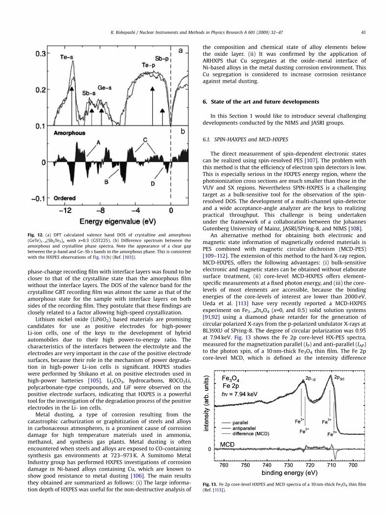
A comparison between amorphous and crystalline valenceband spectra is shown in Fig. 11(b). Astonishingly, both the phasesshow very similar spectra. The resemblance becomes stronger asthe composition x increases. This result is in clear contrast to thecase of amorphous Si, where a drastic change in valence bandstructure from that of crystalline Si takes place due to theinevitably introduced breaks of the rigid sp3 bonding. One of theinteresting features of the amorphous spectra is the appearance ofa clear band-gap between the cation s-band and the p-band. Thelone pair s-bands exhibit very weak dispersions, and thusshould reflect local randomness in the line shape. In case of GeTe,the s-band line-widths are obviously broader in the amorphousphase. In GST225 (x=1/3), they are almost the same in thecrystalline and amorphous phases. This apparently shows thatlocal randomness in the crystalline phase is already as heavy asthat in the amorphous phase. The unusual resemblance of theelectronic structures between the amorphous and crystallinephases is considered to be an essential key to the fast reversiblephase change in GST. A very recent DFT calculation of the DOS byAkola and Jones [103], reproduced the overall spectral featuresand also the appearance of the bandgap mentioned above, asshown in Fig. 12.
5.3. Industrial applications
Here I would like to introduce three typical examples of HXPESapplications to industrial problems. Nakai et al. of Toshiba Ltd.performed, for the first time, a HXPES investigation of theinfluence of interface layers on the chemical and electronic statesof a phase-change GeTe-Bi2Te3 compound (GBT) recordingmaterial [104]. The samples used have the same film structureas re-writable HD DVD media suitable for fast over-write, and are
(i)
ZnS–SiO2/IF/GeBiTe/IF/ZnS–SiO2/Ag alloy/PC substrate, and (ii) ZnS–SiO2/GeBiTe/ZnS–SiO2/Ag alloy/PC substrate.The ‘IF’ in (i) represents interlayers located above and below theGBT recording layer. The GBT valence band spectra near the VBMwere observed through the bandgap of a ZnS-SiO2 overlayer. Nakaiet al. showed that by closely examining the Ge and Te peaks, thebonding state of the elements in the amorphous state of the
ARTICLE IN PRESS
Fig. 12. (a) DFT calculated valence band DOS of crystalline and amorphous
(GeTe)1�x(Sb2Te3)x with x=0.3 (GST225). (b) Difference spectrum between the
amorphous and crystalline phase spectra. Note the appearance of a clear gap
between the p-band and Ge–Sb s bands in the amorphous phase. This is consistent
with the HXPES observations of Fig. 11(b) (Ref. [103]).
Fig. 13. Fe 2p core-level HXPES and MCD spectra of a 10 nm-thick Fe3O4 thin film
(Ref. [113]).
K. Kobayashi / Nuclear Instruments and Methods in Physics Research A 601 (2009) 32–47 41
phase-change recording film with interface layers was found to becloser to that of the crystalline state than the amorphous filmwithout the interface layers. The DOS of the valence band for thecrystalline GBT recording film was almost the same as that of theamorphous state for the sample with interface layers on bothsides of the recording film. They postulate that these findings areclosely related to a factor allowing high-speed crystallization.
Lithium nickel oxide (LiNiO2) based materials are promisingcandidates for use as positive electrodes for high-powerLi-ion cells, one of the keys to the development of hybridautomobiles due to their high power-to-energy ratio. Thecharacteristics of the interfaces between the electrolyte and theelectrodes are very important in the case of the positive electrodesurfaces, because their role in the mechanism of power degrada-tion in high-power Li-ion cells is significant. HXPES studieswere performed by Shikano et al. on positive electrodes used inhigh-power batteries [105]. Li2CO3, hydrocarbons, ROCO2Li,polycarbonate-type compounds, and LiF were observed on thepositive electrode surfaces, indicating that HXPES is a powerfultool for the investigation of the degradation process of the positiveelectrodes in the Li- ion cells.
Metal dusting, a type of corrosion resulting from thecatastrophic carburization or graphitization of steels and alloysin carbonaceous atmospheres, is a prominent cause of corrosiondamage for high temperature materials used in ammonia,methanol, and synthesis gas plants. Metal dusting is oftenencountered when steels and alloys are exposed to CO-containingsynthesis gas environments at 723–973 K. A Sumitomo MetalIndustry group has performed HXPES investigations of corrosiondamage in Ni-based alloys containing Cu, which are known toshow good resistance to metal dusting [106]. The main resultsthey obtained are summarized as follows: (i) The large informa-tion depth of HXPES was useful for the non-destructive analysis of
the composition and chemical state of alloy elements belowthe oxide layer. (ii) It was confirmed by the application ofARHXPS that Cu segregates at the oxide–metal interface ofNi-based alloys in the metal dusting corrosion environment. ThisCu segregation is considered to increase corrosion resistanceagainst metal dusting.
6. State of the art and future developments
In this Section 1 would like to introduce several challengingdevelopments conducted by the NIMS and JASRI groups.
6.1. SPIN-HAXPES and MCD-HXPES
The direct measurement of spin-dependent electronic statescan be realized using spin-resolved PES [107]. The problem withthis method is that the efficiency of electron spin detectors is low.This is especially serious in the HXPES energy region, where thephotoionization cross sections are much smaller than those in theVUV and SX regions. Nevertheless SPIN-HXPES is a challengingtarget as a bulk-sensitive tool for the observation of the spin-resolved DOS. The development of a multi-channel spin-detectorand a wide acceptance-angle analyzer are the keys to realizingpractical throughput. This challenge is being undertakenunder the framework of a collaboration between the JohannesGutenberg University of Mainz, JASRI/SPring-8, and NIMS [108].
An alternative method for obtaining both electronic andmagnetic state information of magnetically ordered materials isPES combined with magnetic circular dichroism (MCD-PES)[109–112]. The extension of this method to the hard X-ray region,MCD-HXPES, offers the following advantages: (i) bulk-sensitiveelectronic and magnetic states can be obtained without elaboratesurface treatment, (ii) core-level MCD-HXPES offers element-specific measurements at a fixed photon energy, and (iii) the core-levels of most elements are accessible, because the bindingenergies of the core-levels of interest are lower than 2000 eV.Ueda et al. [113] have very recently reported a MCD-HXPESexperiment on Fe3�xZnxO4 (x=0, and 0.5) solid solution systems[91,92] using a diamond phase retarder for the generation ofcircular polarized X-rays from the p-polarized undulator X-rays atBL39XU of SPring-8. The degree of circular polarization was 0.95at 7.94 keV. Fig. 13 shows the Fe 2p core-level HX-PES spectra,measured for the magnetization parallel (IP) and anti-parallel (IAP)to the photon spin, of a 10 nm-thick Fe3O4 thin film. The Fe 2pcore-level MCD, which is defined as the intensity difference

ARTICLE IN PRESS
K. Kobayashi / Nuclear Instruments and Methods in Physics Research A 601 (2009) 32–4742
between the IP and IAP spectra, is shown at the bottom of thefigure. The Fe 2p3/2 and 2p1/2 main peaks correspond to the Fe3+
component, while the shoulder structures at the lower bindingenergy side of the main peaks correspond to the Fe2+ components.The Fe 2p core-level MCD spectrum shows a positive peak atEB�710 eV and also a strong negative peak at EB�708 eV, aroundthe shoulder structure of the Fe 2p3/2 photoemission spectra. Thesign of the MCD in the Fe 2p1/2 region is opposite to that in the Fe2p3/2 region.
The structure of Fe3O4 can be rewritten as;
½Fe3þ ð#: 5mBÞ�AO½Fe3þ
þ ð": 5mBÞFe2þ ð": 4mBÞ�BO3,
where A and B denote the sites of metallic ions in the normalspinel structure, and arrows denote the directions of the magneticmoments, which are also designated beside the arrows. The netmagnetic moment of the Fe3+ ions vanishes due to the compensa-tion between the A and B sites, and only the magnetic moment ofthe Fe2+ ions at the B site remains. This is consistent with theobservation of MCD signal only for the Fe2+ ions in Fe3O4, asshown in Fig. 13.
An application of MCD-HXPES to the valence band is alsoexpected to be useful for investigations of the electronic andmagnetic states. The valence band MCD-HXPES can be compar-able with spin-resolved band calculations, because it is possible tocalculate the valence band MCD-HXPES under the dipoleapproximation. Another application of MCD-HXPES is to probethe depth information for both electronic and magnetic states.The TOA dependence of MCD-HXPES enables ones to probe thedepth information.
Fig. 15. Intensity profile and differential intensity profile for (a) horizontal and (b)
vertical focusing (Ref. [114]).
6.2. HXPES with a micro/nano focused beam
Focusing of the X-ray beam is one of the crucial points for highresolution and high throughput in HXPES, as has already beenmentioned. Yang et al. have achieved a spot size of 1.1mm�0.97mm by combining high precision K-B mirrors [114] with a HXPESspectroscopy system for the first time. The HXPES spectra of goldfilm around the Fermi edge indicate an improvement in totalenergy resolution by about 20 meV using the K-B system. Theexperiments were performed at the undulator beamline BL47XUof SPring-8. Fig. 14 shows the optical configuration of the K-Bmirrors system, installed downstream of the Si channel-cut post-monochromator. Both the vertical and horizontal focusing mirrors(MV and MH) are elliptical mirrors, with shape errors of about2 nm and lengths of 100 mm. The silicon mirror surfaces werecoated with Pt film, resulting in a reflectivity of about 89.5%. Thefocal length is 258 mm for MV and 154 mm for MH. The glancingangle is 4.06 mrad for MV and 3.6 mrad for MH. The distance
Fig. 14. Optical configuration of
between the two mirrors is 150 mm, and the working distance ofthe K-B system is 100 mm to the focus point. An incident slit of300mm�300mm is located 10.65 m upstream from the center ofMV. To ensure stability of the K-B system, it is mounted on a rigidbase separate from the HXPES system. The alignment ofparameters such as the glancing angle and the perpendicularitybetween the two mirrors was achieved using a mirrormanipulator with a high degree of accuracy [10]. Behind the K-Bsystem, a wire scan system with a piezo-actuated translationstage was placed at the focal position. The X-ray intensity ismonitored using an ionization chamber located behind the wirescan system.
Figs. 15(a) and (b) show the measured intensity profiles (solidsquares) and their derivative profiles (open circles) for horizontalfocusing and vertical focusing. The solid curves are fits to thederivative profiles using Gaussian functions. The FWHMs of thefitted curves indicate that a beam size of 1.10mm (H)�0.98mm(V) was achieved. Figs. 16(a) and (b) show the Fermi edge spectraand 4f core level spectra of Au measured using the K-B mirrors,and Figs. 16(c) and (d) show the same spectra recorded withoutusing the mirrors. By fitting the Fermi edge spectra (solid line) theenergy resolution is shown to be reduced to 217 meV by using K-Bmirrors, 20 meV better than without the K-B mirrors (Fig. 16(c)).Comparing the Au 4f spectra with and without the K-B mirrorsystem, the intensity is reduced by about a factor of 30 by the K-Bmirrors (Fig. 16(b) and (d)). The dominant factor for this intensityloss is that the K-B mirror system used in this experiment spillsX-rays considerably due to the small numerical aperture ofthe mirrors (0.7 mm), which makes precise alignment difficult.
the K-B mirrors (Ref. [114]).

ARTICLE IN PRESS
Fig. 16. HXPES spectra of Au EF (a) with K-B mirrors and (b) without K-B mirrors, and HXPES spectra of Au 4f (c) with K-B mirrors and (d) without K-B mirrors (hn=7.94 keV)
(Ref. [114]).
K. Kobayashi / Nuclear Instruments and Methods in Physics Research A 601 (2009) 32–47 43
Another factor is the air path introduced upstream of the HXPESchamber of about 2 m which is necessary for the K-B mirror andassociated alignment instruments. This reduces the beam flux byabsorption and scattering by about a factor of 0.5. The reflectivityof each mirror is 89.5%, resulting in a total flux loss of about 20%.In future the flux loss problem will be addressed by using largermirrors (�200 mm long), and by purging the air from the opticalpath using He gas.
6.3. 3D chemical analysis and laboratory HXPES
As mentioned above, HXPES development has been verysuccessful at third generation synchrotron radiation facilities.This tempts us to develop advanced instrumentation for expand-ing further applications of HXPES. One of the targets to challengeis the three-dimensional analysis of chemical states in advancedmaterials and devices by TOA dependence measurements of corelevel spectra using micro-nano focused X-ray excitation. Nano-scale thin layers and their stacks, the thicknesses of which matchwell the probing depths of HXPES, play essential roles to bear thefunctionalities in these advanced materials and devices. Anotherattractive target for us is the development of a laboratory HXPESsystem with practical throughput. If this is realized, it is expectedto be very effective for offering the opportunities of HXPESapplications to users widespread in various fields of science andtechnology. Combining the above two challenges, we began in2006 a project for the development of a HXPES spectrometer for3D chemical state analysis under the framework of a SENTANproject of the Japan Science and Technology Agency (JST). Themain purpose of the project consists of two parts. (1) thedevelopment of a system which utilizes a micro-nano focused
X-ray beam at a SPring-8 hard X-ray undulator beamline, and (2)the development of a laboratory system using a focused Cr Kamonochromatic source.
The development of a wide-acceptance objective lenswith angle-resolution capability is a key to both thesetargets. Daimon and Matsuda have designed an objectivelens to fulfill these specifications using an ellipsoidal meshelectrode in the first stage of the lens [115,116]. The mostcrucial point in this objective lens development is thehigh-precision fabrication of the mesh electrode. The specifica-tions we need for the objective lens are as follows: 7351–451acceptance angle, 771–91 exit angle, a spot size at the exitfocusing point of 0.5 mm or less, 11 angular resolution,and maximum operating voltage at electrodes of 8–10 keV.Fig. 17(a) shows the results of a simulation of the objective lens.An ellipsoidal metal mesh is adopted in the first stage electrode ofthe lens. We have manufactured several prototypes and testedthem using a focused electron gun with minimum spot size of2mm. The coincidence between the lens parameter sets whichwere obtained experimentally by minimizing the focus spotsize and those obtained by simulation was excellent. Anexample of the observed focused spot image and its profile areshown in Fig. 17(b) and (c).
As for the beamline-based focused X-ray sources, the K-Bmirror system described in the preceding section will be applied.For the laboratory system, we have developed a CrKa (5.4 keV)focused X-ray source. The water cooled Cr target is excited by afocused electron beam, and the emitted X-rays are monochroma-tized and focused on to the sample surface using a bent crystalmonochromator with a 300 mm Roland circle. The X-ray spot isvariable from 10mm (1.25 W) to 200mm (50 W), and TOAdependencies of HXPES spectra are measurable without

ARTICLE IN PRESS
Fig. 17. Structure and electron trajectory simulation of the wide acceptance objective lens. (b) Focused spot at the exit of the wide acceptance objective lens. (c) Cross-
section profile of the focused spot. (unpublished. H. Matsuda, M. Kobata, H. Daimon, and K. Kobayashi.)
3050 3100 3150 3200 32500.00.0
2.0x10⁵
4.0x10⁵
6.0x10⁵
8.0x10⁵
1.0x10⁶
1.2x10⁶
Inte
nsity
(ar
b.un
its)
Without lens
With Lens
Kinetic Energy
Fig. 18. Au 3d spectra measured with and without the wide acceptance objective
lens by Cr Ka excitations of 25 W, and 100mm spot size. The acquisition time was
15 min for both spectra. The throughput is enhanced 7.5 times by the wide
acceptance objective lens. (unpublished. M. Kobata, H. Iwai, H. Yamazui, H.
Takahashi, M. Kodama, A. Tanaka, M. Suzuki, H. Daimon and K. Kobayashi.)
K. Kobayashi / Nuclear Instruments and Methods in Physics Research A 601 (2009) 32–4744
rotating the sample. This makes possible the 2D mappingof depth profiles by scanning the focused X-ray spot on thesample surface.
Here some of the preliminary results are introduced to provethe feasibility of this laboratory HXPES system which is still underdevelopment. Fig. 18 shows a comparison of Au 3d spectrarecorded using a VG Scienta R4000 10 kV analyzer with andwithout the new objective lens. The experimental conditions wereas follows; beam size 200mm, TOA 871, sample current 29 nA, passenergy 200 V, analyzer entrance slit 4 m. The acquisition time forthe Au 3d spectrum with the objective lens was 16 min.Enhancement of the throughput was confirmed to be a factor of7 at the present stage. The angular acceptance and angularresolution were estimated using a test sample to generatephotoelectrons from a thin linear region equipped with a multi-slit hemi-cylinder for collimation. As shown in Fig. 19, anacceptance angle of7351 and resolution of less than 11 wasestablished. Considering that there still remains room for furtherimprovements in the objective lens and its matching with theanalyzer, we believe that this system shows considerable promiseas a laboratory HAXPES instrument with practical throughput.

ARTICLE IN PRESS
Emission Angle (deg)
3208eV
3206
3204
3202
3200
3198
3196
Kin
etic
Ene
rgy
(eV
)
035 35
Inte
nsit
y (a
rb.u
nits
)
Emission Angle (deg)
Fig. 19. The angular resolution of the wide acceptance objective lens was tested using a test device composed of a Au plate, in front of which is mounted a combination of a
long slit and a cylindrical multi-slit. (a) Image recorded Au 3d5/2 peak on the 2D detector in the angular mode of the VG Scienta 10 kV analyzer. (b) Profile of the image
along the line indicated in (a). A 7351 acceptance angle with angular resolution better than 11 is evident in this result. (Period of the multi-slit is 2.81) (M. Kobata, I. Iwai, H.
Yamazui, H. Takahashi, M. Kodama, A. Tanaka, M. Suzuki, H. Matsuda, H. Daimon and K. Kobayashi.)
K. Kobayashi / Nuclear Instruments and Methods in Physics Research A 601 (2009) 32–47 45
7. Conclusion
High-resolution HXPES using synchrotron X-rays is a verypowerful and versatile tool for investigations in a wide range offields throughout solid state physics, applied physics, materialsscience and chemistry, device R&D and analytical science andtechnology. HXPES is not only complementary to conventionalPES, but also opens up possibilities in new fields which have notbeen accessible to conventional PES. To further widen the fields ofapplication to increase the user base, a laboratory HXPES systemwith practical throughput is being developed. This will help toexpand HXPES utilization even further.
Acknowledgements
Rapid growth in HXPES research fields as described in the textis the fruit of stimulating competitions and collaborations amongpioneering groups, that is, ID 32, VOLPE project (ID16), andSpanish beamline (BM16) groups at ESRF, JASRI (BL4XU, andBL46XU), RIKEN (BL29XU), Osaka University (RIKEN beamline atBI19LXU), and NIMS (BL15XU) groups at SPring-8, and also HIKEgroup at BESSY II (KMC-1). The progress of HXPES activities arealso supported by cooperation in pioneering groups with analyzermakers such as VG SCIENTA AB, SPECS GmbH, FOCUS GmbH, MBScience AB, and Physical Electronics. At SPring-8, constructions ofX-ray optics in all the HXPES beamlines are due to collaborationswith T. Ishikawa and his co-workers. The prototype of theexperimental configuration was mostly established during theearly stage of the test experiments by Y. Takata, whose contribu-tions during the raise of HXPES at BL29XU were inevitable.Collaborations among JASRI, RIKEN, HiSOR, and JAEA were alsoinevitable, resulting in realizing HXPES experimental stationsopened for public use only 1–2 years after the success of the firsttest experiment. Above all, active users’ contributions were themost essential factors of the rapid progress of HXPES applicationsto wide spreading basic, applied, and industrial research fields.The author is grateful to E. Ikenaga, J.J. Kim, M. Kobata, and S. Uedafor their devoting works during the incubation period of HXPESpublic activities at BL4XU. The author is also thankful to Y. Takeda,Y. Saito, M. Arita, K. Shimada, H. Namatame, M. Taniguchi, E.Ikenaga, S. Ueda, and H. Yoshikawa, for their efforts during theconstruction period of HXPES station at BL15XU.
The author is grateful to E. Ikenaga for his kindness in offeringunpublished data obtained during his zealous work at BL47XU.The development of the 3D chemical analysis technique which isintroduced in the final part of this article is supported by a JST‘‘Sentan’’ project, with the involvement of M. Kobata and H. Iwai ofNIMS, H. Matsuda and H. Daimon of NAIST, E. Ikenaga, K. Yang,M. Machida, and J.-Y.Son of JASRI, and M. Suzuki, H. Yamazui,H. Takahashi, M. Kodama, and A. Tanaka of ULVAC PHI, who arethanked for the unpublished data presented in this article on thistopic. Critical readings of the manuscript by J. Harries and S. Uedaare much appreciated.
References
[1] K. Siegbahn, Nucl. Instr. and Meth. A 54 (2005) 1 (Proceedings of theWorkshop on Hard X-ray Photoelectron Spectroscopy, European SynchrotronRadiation Facility, Grenoble, France, September 11–12, 2003).
[2] K. Siegbahn, C. Nordling, A. Fahlman, R. Nordberg, S.-E. Karlsson, I. Lindgren,ESCA Atomic, Molecular and Solid State Structure Studied by Means ofElectron Spectroscopy, Almqvist and Wiksells AB, Stockholm, 1967.
[3] K. Kobayashi, M. Yabashi, Y. Takata, T. Tokushima, S. Shin, K. TamasakuD. Miwa, T. Ishikawa, H. Nohira, T. Hattori, Y. Sugita, O. Nakatsuka, A. SakaiS. Zaima, Appl. Phys. Lett. 83 (2003) 1005.
[4] I. Lindau, P. Pianetta, S. Doniach, W. Spicer, Nature 250 (1974) 214.[5] P.H. Citrin, P. Eisenberger, R.C. Hewitt, Phys. Rev. Lett. 41 (1978) 309.[6] J. Zegenhagen, Surf. Sci. Rep. 18 (1993) 202 and references therein.[7] G.S. Brown, et al., Phys. Rev. Lett. 45 (1980) 1937.[8] L.E. Cox, et al., Phys. Rev. B 31 (1985) 2467.[9] A. Bianconi, et al., Phys. Rev. B 39 (1989) 3380.
[10] W. Drube, A. Lessmann, G. Materlik, Rev. Sci. Instr. 63 (1992) 1138.[11] W. Drube, A. Lessmann, G. Materlik, Jpn. J. Appl. Phys. 32 (Suppl. 32-2) (1992)
173.[12] L. Braicovich, N.B. Brookes, C. Dallera, M. Salvietti, G.L. Olcese, Phys. Rev. B 56
(1997) 15047.[13] P. Le Fevre, H. Magnan, D. Chandesris, J. Vogel, V. Formoso, F. Comin, Phys. Rev.
B 58 (1998) 1080.[14] H. Yamamoto, Y. Baba, T.A. Sasaki, Surf. Sci. 349 (1996) L133.[15] W. Drube, et al., Rev. Sci. Instr. 66 (1995) 1668.[16] G.J. Jackson, et al., Phys. Rev. Lett. 84 (2000) 119.[17] J.C. Woicik, et al., Phys. Rev. Lett. 89 (2002) 077.[18] Y. Takata, K. Tamasaku, T. Tokushima, D. Mia, S. Shin, T. Ishikawa, M. Yabashi,
K. Kobayashi, J.J. Kim, T. Yao, T. Yamamoto, M. Arita, H. NamatameM. Taniguchi, Appl. Phys. Lett. 84 (2004) 4310.
[19] C. Dallera, L. Braicovich, L. Duo, G. Panaccione, G. Paolicelli, B. CowieJ. Zegenhagen, Appl. Phys. Lett. 85 (2004) 4532.
[20] P. Torelli, et al., Rev. Sci. Instrum. 57 (2005) 023909.[21] S. Ties, C. Kunz, B.C.C. Cowie, T.L. Lee, M. Reiner, J. Zegenhagen, Solid State
Commun. 132 (2004) 589.[22] Y. Takata, et al., Nucl. Instr. and Meth. A 54 (2005) 50 (Proceedings of the
Workshop on Hard X-ray Photoelectron Spectroscopy, European SynchrotronRadiation Facility, Grenoble, France, September 11–12, 2003).

ARTICLE IN PRESS
K. Kobayashi / Nuclear Instruments and Methods in Physics Research A 601 (2009) 32–4746
[23] G. Panaccione, G. Cautero, A. Fondacaro, M. Grioni, P. Lacovig, G Monaco,F Offi, G. Paolicelli, M. Sacci, G. Stefani, T. Torelli, Nucl. Instr. and Meth. A 54(2005) 56.
[24] F. Offi, A. Fondacaro, G. Paolicelli, A. De Luisa, G. Stefani, Nucl. Instr. and Meth.A 55 (2005) 454.
[25] J.R. Rubio-Zuazo, G.R.. Castero, Nucl. Instr. and Meth. A 55 (2005) 64.[26] C. Kunz, S. Tiess, B. Cowie, T.-L. Lee, J. Zegenhagen, Nucl. Instr. and Meth. A 55
(2005) 73.[27] Y. Takata et al., Proceedings of 9th International Conference on Synchrotron
Radiation Instrumentation, Daegu, Korea, 28 May–2 June 2006, in: J.Y. Choi,S. Rah, AIP Conference Proceedings, vol. 879, 2006, pp. 1597–1602.
[28] F. Schafer, M. Mertin, M. Gorgoi, BESSY Annual Report, 2006, pp. 211–213.[29] K. Kobayashi, E. Ikenaga, J.J. Kim, M. Kobata, S. Ueda, Nanotechnology and
Industrial Applications of hard X-ray Photoemission Spectroscopy, Proceed-ings of 9th International Conference on Synchrotron Radiation Instrumenta-tion, Daegu, Korea, 28 May–2 June 2006, in: J.Y. Choi, S. Rah, AIP ConferenceProceedings, vol. 879, 2006, pp. 1539–1544.
[30] HAXPES experimental station is planned at P09 Resonant Scattering/Diffraction Beamline /http://petra3.desy.de/S.
[31] M. Sacchi, F. Offi, P. Torelli, A. Fondacaro, C. Spezzani, M. Cautero, G. CauteroS. Houtari, M. Grioni, R. Delaunay, M. Fabrizioli, G. Vanko, G. MonacoG. Paolicelli, G. Stefani, G. Panaccione, Phys. Rev. B 71 (2005) 155117.
[32] J.C. Woicik, Nucl. Instr. and Meth. A 547 (2005) 227.[33] I. Vartanyantsa, T.-L. Leeb, S. Thiessb, J. Zegenhagen, Nucl. Instr. Meth. A 547
(2005) 196.[34] T.-L. Lee, S. Warren, L.X. Cao, S. Thieb, B.C.C. Cowie, J. Zegenhagen, Nucl. Instr.
Meth. 547 (2005) 216.[35] T. Fujii, M. Kimura, H. Yoshikawa, S. Fukushima, Solid State Commun. 136
(2005) 375.[36] K. Hirose, H. Nohira, K. Azuma, T. Hattori, Progr. Surf. Sci. 82 (2007) 3.[37] J. Rubio-Zuazo, G.R. Castro, J. Phys. Conf. Ser. 100 (2008) 012042.[38] S.-H. Yang, B.C. Sell, C.S. Fadley, J. Appl. Phys. 103 (2008) 07C519.[39] E. Holmstrom, W. Olovsson, I.A. Abrikosov, A.M.N. Niklasson, B. Johansson,
Phys. Rev. Lett. 97 (2006) 266106.[40] J. H. Scofield, Theoretical Photoionization Cross Section from 1–1500 keV,
January 12, UCRL-51326, 1973.[41] J.-J. Yeh, I. Lindau, Atomic Data Nucl. Data Tables 32 (1985) 1.[42] M.B. Trazhaskovskkaya, V.I. Nefedov, V.G. Yarzhemsky, Atomic Data Nucl.
Data Tables 77 (2001) 97;M.B. Trazhaskovskkaya, V.I. Nefedov, V.G. Yarzhemsky, Atomic Data Nucl. DataTables 82 (2002) 257;M.B. Trzhaskovskaya, V.K. Nikulin, V.I. Nefedov, V.G. Yarzhemsky, Atomic DataNucl. Data Tables 92 (2006) 245.
[43] K. Kobayashi, Y. Takata, T. Yamamoto, J.-J. Kim, H. Makino, K. TamasakuM. Yamashi, D. Miwa, T. Ishikawa, S. Shin, T. Yao, Jpn. J. Appl. Phys. 43 (2004)L1029.
[44] K. Kobayashi, Nucl. Instr. and Meth. A 54 (2005) 98 (Proceedings of theWorkshop on Hard X-ray Photoelectron Spectroscopy, European SynchrotronRadiation Facility, Grenoble, France, September 11–12, 2003).
[45] G. Panaccionel, G. Cautero, M. Cautero, A. Fondacaro, M. Grioni, P. LacovigG. Monaco, F. Offi, G. Paolicelli, M. Sacchi, N. Stojıc, G. Stefani, R. TommasiniP. Torelli, J. Phys.: Condens. Matter 17 (2005) 2671.
[46] H. Yoshikawa et al., private communication.[47] Y. Takata, Y. Kayanuma, M. Yabashi, K. Tamasaku, Y. Nishino, D. Miwa
Y. Harada, K. Horiba, S. Shin, S. Tanaka, E. Ikenaga, K. Kobayashi, Y. SenbaH. Ohashi, T. Ishikawa, Phys. Rev. B 5 (2007) 233404.
[48] R.L. Mossbauer, Z. Phys. 151 (1958) 124.[49] Y. Takata, Y. Kayanuma, S. Oshima, S. Tanaka, M. Yabashi, K. Tamasaku,
Y. Nishino, M. Matsunami, R. Eguchi, A. Chainani, M. Oura, T. Takeuchi,Y. Senba, H. Ohashi, and T. Ishikawa, Phys. Rev. Lett. 100 (2008) 137601.
[50] Y. Takata, et al., J. Electron Spectrosc. Relat. Phenom. 144-147 (2005) 1063.[51] T. Ishikawa, K. Tamasaku, M. Yabashi, Nucl. Instr. and Meth. A 54 (2005) 42
(Proceedings of the Workshop on Hard X-ray Photoelectron Spectroscopy,European Synchrotron Radiation Facility, Grenoble, France, September 11-12,2003).
[52] A. Sekiyama, T. Iwasaki, K. Matsuda, Y. Saitoh, Y. Onuki, S. Suga, Nature(London) 403 (2003) 396.
[53] H. Sato, et al., Phys. Rev. Lett. 93 (2004) 246404.[54] L. Moreschini, et al., Phys. Rev. B 75 (2007) 035113.[55] S. Suga et al., Presented at HAXPES 06 Workshop Held at SPring-8, September
2006, unpublished.[56] A. Yamasaki, S. Imada, H. Higashimichi, H. Fujiwara, T. Saita, T. Miyamachi
A. Sekiyama, H. Sugawara, D. Kikuchi, H. Sato, A. Higashiya, M. YabashiK. Tamasaku, D. Miwa, T. Ishikawa, S. Suga, Phys. Rev. Lett. (2007)156402.
[57] K. Horiba, et al., Phys. Rev. Lett. 93 (2004) 236401.[58] M. Taguchi, M. Altarelli, Surf. Rev. Lett. 9 (2002) 1167.[59] O. Gunnarsson, K. Schonhammer, in: K.A. Gschneidner, L. Eyring, S. Hufner
(Eds.), Handbook on the Physics and Chemistry of Rare Earths, vol. 10, ElsevierScience Publishers BV, New York, 1987.
[60] H. Tanaka, Y. Takata, K. Horiba, M. Taguchi, A. Chainani, S. Shin, D. MiwaK. Tamasaku, Y. Nishino, T. Ishikawa, E. Ikenaga, M. Awaji, A. TakeuchiT. Kawai, K. Kobayashi, Phys. Rev. B 73 (2006) 094403.
[61] N. Kamakura, et al., Europhys. Lett. 68 (2004) 557.[62] M. Taguchi, et al., Phys. Rev. Lett. 95 (2005) 177002.[63] M. Taguchi, et al., Phys. Rev. B 71 (2005) 155102.
[64] G. Panaccione, F. Offi, P. Torelli, G. Vanko, O. Tjernberg, P. Lacovig, A. Guarino,A. Fondacaro, A. Nigro, M. Sacchi, N.B. Brookes, G. Monaco, Phys. Rev. B 77(2008) 125133.
[65] G. Panaccione, M. Altarelli, A. Fondacaro, A. Georges, S. Huotari, P. LacovigA. Lichtenstein, P. Metcalf, G. Monaco, F. Offi, L. Paolasini, A. PoteryaevO. Tjernberg, M. Sacchi, Phys. Rev. Lett. 97 (2006) 116401.
[66] G. Panaccione, F. Offi, M. Sacci, P. Torelli, C. R. Phys. 9 (2008) 524.[67] F. Offi, P. Torelli, M. Sacchi, P. Lacovig, A. Fondacaro, G. Paolicelli, S. Huotari
G. Monaco, C.S. Fadley, J.F. Mitchell, G. Stefani, G. Panaccione, Phys. Rev. B 75(2007) 014422.
[68] K. Yamamoto, et al., J. Electron Spectrosc. Relat. Phenom. 144–147 (2005) 553.[69] R. Eguchi, et al., J. Electron Spectrosc. Relat. Phenom. 156–158 (2007) 421.[70] A. Yamazaki, S. Imada, H. Higashimichi, F. Fujwara, T. Saita, T. Miyamachi
A. Sekiyama, H. Sugawara, D. Kikuchi, H. Sato, A. Higashiya, M. YabashiK. Tamasaku, D. Miwa, T. Ishikawa, S. Suga, J. Electron Spectrosc. Relat.Phenom. 156–158 (2007) 323.
[71] K. Terai, K. Yoshii, Y. Takeda, S.I. Fujimori, Y. Saitoh, K. Ohwada, T. InamiT. Okane, M. Arita, K. Shimada, H. Namatame, M. Taniguchi, K. KobayashiM. Kobayashi, A. Fujimori, Phys. Rev. B 77 (2008) 115128.
[72] M. Sawada, et al., Physica B 383 (2006) 152.[73] M. Taguchi, M. Matsunami, Y. Ishida, R. Eguchi, A. Chainani, Y. Takata, M.
Yabashi, K. Tamasaku, Y. Nishino, T. Ishikawa, Y. Senb, H. Ohashi, S. Shin, Phys.Rev. Lett. 100 (2008) 206401.
[74] International technology roadmap for semiconductors: /http://public.itrs.net/S.
[75] T. Hattori, H. Nohira, K. Azuma, W. Sakai, K. Nakajima, M. Suzuki, K. KimuraY. Sugita, E. Ikenaga, K. Kobayashi, Y. Tanaka, H. Kondo, S. Zaima, Int. J. HighSpeed Electron Systems 16 (2006) 353.
[76] H. Nohira, et al., ECS Trans. 1 (2005) 87.[77] H. Nohira, T. Matsuda, K. Tachi, Y. Shiino, J. Song, Y. Kuraki, Ng. Jin Aun
P. Ahmet, K. Kalishima, T. Tsutsui, E. Ikenaga, K. Kobayashi, H. Iwai, T. Hattori,ECS Trans. 3 (2006) 169.
[78] K. Kimura, K. Nakajima, M. Zhao, H. Nohira, T. Hattori, M. Kobata, E. Ikenaga,J.J. Kima, K. Kobayashi, T. Conard, W. Vandevorst, Surf. Interface Anal. 40(2008) 423.
[79] E. Ikenaga, I. Hirosawa, A. Kitano, Y. Takata, A. Muto, T. Maeda, K. ToriiH. Kitajima, T. Arikado, A. Takeuchi, M. Awaji, K. Tamasaku, T. IshikawaS. Komiya, K. Kobayashi, J. Electron Spectrosc. Relat. Phenom. 144–147 (2005)491.
[80] C.G. Jin, Y. Sasaki, K. Okashita, H. Tamura, H. Ito, B. Mizuno, T. Okumura,M. Kobata, J.J. Kim, E. Ikenaga, K. Kobayashi, Extracted Abstract, in: The 7thInternational Workshop on Junction Technology, 2006.
[81] C.G. Jin, Y. Sasaki, K. Okashita, B. Mizuno, M. Kobata, J.J. Kim, E. Ikenaga,K. Kobayashi, Extracted Abstract, in: The 7th International Workshop onJunction Technology, 2007.
[82] K. Hirose, M. Kihara, D. Kobayashi, H. Okamoto, S. Shinagawa, H. NohiraE. Ikenaga, M. Higuchi, A. Teramoto, S. Sugawa, T. Ohmi, T. Hattori, Appl. Phys.Lett. 89 (2006) 154103.
[83] E. Martinez, O. Renault, L. Clavelier, C. Le Royer, J.-M. Hartmann, V. LoupS. Minoret, V. Cosnier, Y. Campidelli J. Zegenhagen, T.-L. Lee, J. Vac. Sci.Technol. B 25 (2007) 86.
[84] Y. Hijikata, H. Yaguchi, S. Yoshida, Y. Takata, K. Kobayashi, H. Nohira, T. Hattori,J. Appl. Phys. 100 (2006) 053710.
[85] H. Wadati, Y. Hotta, A. Fujimori, T. Susaki, H.Y. Hwang, Y. TakataK.M. Matsunami, S. Shin, M. Yabashi, K. Tamasaku, Y. Nishino, T. Ishikawa,Phys. Rev. B 77 (2008) 045122.
[86] S. Wurmehll, G.H. Fecherl, K. Krothl, F. Kronast, H. A Durr, Y. TakedaY. Saitoh, K. Kobayashi, H. Ji Lin, G. Schonhense, C. Felser, J. Phys. D 39 (2006)803.
[87] B. Balke, G.H. Fecher, H.C. Kandpal, C. Felser, K. Kobayashi, E. Ikenaga, J.J. Kim,S. Ueda, Phys. Rev. B 74 (2006) 104405.
[88] G.H. Fecher, B. Balke, S. Ouardi, C. Felser, E. Ikenaga, J.J. Kim, S. UedaK. Kobayashi, J. Phys. D: Appl. Phys. 40 (2007) 1576.
[89] G.H. Fecher, B. Balke, A. Gloskowskii, S. Ouardi, C. Felser, T. IshikawaM. Yamamoto, Y. Yamashita, H. Yoshikawa, S. Ueda, K. Kobayashi, Appl. Phys.Lett. 92 (2008) 193513.
[90] T. Yanagida, H. Tanaka, T. Kawai, E. Ikenaga, M. Kobata, J.-J. Kim, K. Kobayashi,Phys. Rev. B 73 (2006) 132503.
[91] J. Takaobushi, H. Tanaka, T. Kawai, S. Ueda, J.-J. Kim, M. Kobata, E. IkenagaM. Yabashi, K. Kobayashi, Y. Nishino, D. Miwa, K. Tamasaku, T. Ishikawa, Appl.Phys. Lett. 89 (2006) 242507.
[92] J. Takaobushi, et al., Phys. Rev. B 76 (2007) 205108.[93] M. Osada, M. Itose, Y. Ebina, K. Ono, S. Ueda, K. Kobayashi, T. Sasaki, Appl.
Phys. Lett. 92 (2008) 253110.[94] Y. Toda, H. Yanagi, E. Ikenaga, J.J. Kim, M. Hirano, K. Kobayashi, H. Hosono,
Adv. Mater. 19 (2007) 3564.[95] K. Nomura, T. Kamiya, H. Yanagi, E. Ikenaga, K. Yang, K. Kobayashi, M. Hirano,
H. Hosono, Appl. Phys. Lett. 92 (2008) 202117.[96] J.J. Kim, H. Makino, K. Kobayashi, Y. Takata, T. Yamamoto, T. Hanada
M.W. Cho, E. Ikenaga, M. Yabashi, D. Miwa, Y. Nishino, K. TamasakuT. Ishikawa, S. Shin, T. Yao, Phys. Rev. B 70 (2004) 161315(R).
[97] J.J. Kim, H. Makino, K. Kobayashi, P.P. Chen, E. Ikenaga, M. Kobata, A. Takeuchi,M. Awaji, T. Hanada, M.W. Cho, T. Yao, Phys. Stat. Sol. (c) 3 (2006) 1846.
[98] J.J. Kim, E. Ikenaga, M. Kobata, A. Takeuchi, M. Awaji, H. Makino, P.P. ChenA. Yamamoto, T. Matsuoka, D. Miwa, Y. Nishino, T. Yamamoto, T. YaoK. Kobayashi, Appl. Surf. Sci. 252 (2006) 5602.

ARTICLE IN PRESS
K. Kobayashi / Nuclear Instruments and Methods in Physics Research A 601 (2009) 32–47 47
[99] T. Ohsawa, N. Ohashi, Y. Adachi, I. Sakaguchi, H. Ryoken, K. MatsumotoH. Haneda S. Ueda, H. Yoshikawa, K. Kobayashi, Appl. Phys. Lett. 92 (2008)232108.
[100] T. Yokoya, E. Ikenaga, M. Kobata, H. Okazaki, K. Kobayashi, A. TakeuchiA. Awaji, Y. Takano, M. Nagao, I. Sakaguchi, T. Takenouchi, K. KobayashiH. Kawarada, T. Oguchi, Phys. Rev. B 75 (2007) 205117.
[101] J.-J. Kim, K. Kobayashi, E. Ikenaga, M. Kobata, S. Ueda, T. MatsunagaK. Kifune, R. Kojima, N. Yamada, Phys. Rev. B 76 (2007) 115124.
[102] K. Kobayashi, J.-J. Kim, T. Matsunaga, K. Kifune, E. Ikenaga, M. Kobata,S. Ueda, R. Kojima, N. Yamada, MRS Proceedings 1072 E (2008) 1072-G02-07.
[103] J. Akola, R.O. Jones, Phys. Rev. B 76 (2007) 235201.[104] T. Nakai, M. Yoshiki, N. Ohmachil, Jpn. J. Appl. Phys. Sol. 46 (2007) 3968.[105] M. Shikano, H. Kobayashi, S. Koike, H. Sakaebe, E. Ikenaga, K. Kobayashi
K. Tatsumi, J. Power Sources 174 (2007) 795.[106] T. Doi, K. Kitamura, Y. Nishiyama, N. Otsuka, T. Kudo, M. Sato
E. Ikenaga, K. Kobayashi, T. Hashimoto, Surf. Interface Anal. (2008)329.
[107] S. Hufner, Photoelectron Spectroscopy, 3rd ed, Springer-Verlag, Berlin, 2003;S. Ueda, H. Tanakal, J. Takaobushi, E. Ikenaga, J.-J. Kim, M. Kobata, T. Kawai
H. Osawa, N. Kawamura, M. Suzuki, K. Kobayashi, Appl. Phys. Express 1(2008) 077003.
[108] 2008A0017 (SPring-8 long term proposal approved in 2008A) ‘‘SPINpolarized high resolution HArd X-ray PhotoEmission Spectroscopy SPIN-HAXPES’’, Claudia Felser (Johannes Gutenberg-University, Mainz).
[109] C.M. Schneider, J. Kirschner, Crit. Rev. Solid State Mater. Sci. 20 (1995) 179.[110] L. Baumgarten, C.M. Schneider, H. Petersen, F. Schafers, J. Kirschner, Phys.
Rev. Lett. 65 (1990) 492.[111] B.T. Thole, H.A. Durr, G. van der Laan, Phys. Rev. Lett. 74 (1995) 2371.[112] S. Ueda, S. Imada, Y. Saitoh, T. Muro, M. Kasashima, A. Kimura, A. Kakizaki
S. Suga, J. Electron Spectrosc. Relat. Phenom. 88–91 (1998) 191.[113] S. Ueda, H. Tanaka, J. Takaobushi, E. Ikenaga, J.-J. Kim, M. Kobata, T. Kawai
H. Osawa, N. Kawamura, M. Suzuki, K. Kobayashi, Appl. Phys. Express 1(2008) 077003.
[114] K. Yang, E. Ikenaga, H. Okada, T. Tsumura, Y. Watanabe, K. Yamauchi, andK. Kobayashi, The Conference Name is Pan-American SRI 2008 Meeting,Nucl. Instr. Meth. A.
[115] H. Matsuda, H. Daimon, M. Kato, M. Kudo, Phys. Rev. E 71 (2005) 066503.[116] patent: PCT/jp2004/016602, Japan 2004-208926.