hardware security − smartcards and other tamper−resistant modules · dissolve package in 60 °c...
TRANSCRIPT

Markus G. Kuhn
Computer Laboratory
Hardware Security − Smartcardsand other Tamper−Resistant Modules
http://www.cl.cam.ac.uk/~mgk25/

Applications of Tamper Resistant Modules
Security of cryptographic applications is based on securestorage of secret keys and unobservability of computation
Distributed and mobile applications allow attacker full physicalaccess to hardware over extended period of time
electronic purses
anti-theft protection
software copy protection cellular phones
authentic telemetry
protection of algorithms
pay-TV access control
prepayment meters
financial transaction terminals
...
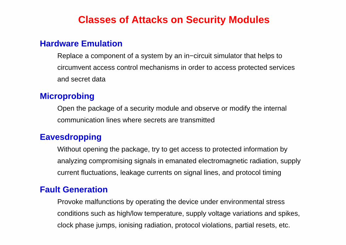
Classes of Attacks on Security Modules
Hardware EmulationReplace a component of a system by an in−circuit simulator that helps to
circumvent access control mechanisms in order to access protected services
and secret data
MicroprobingOpen the package of a security module and observe or modify the internal
Eavesdropping
Provoke malfunctions by operating the device under environmental stress
Without opening the package, try to get access to protected information by
analyzing compromising signals in emanated electromagnetic radiation, supply
current fluctuations, leakage currents on signal lines, and protocol timing
Fault Generation
conditions such as high/low temperature, supply voltage variations and spikes,
clock phase jumps, ionising radiation, protocol violations, partial resets, etc.
communication lines where secrets are transmitted

1)
2)
Heat up card plastic, bend it, and remove chip module
Dissolve package in 60 °C fuming nitric acid, then wash in acetone,
deionized water, and finally isopropanol. The etching should be
carried out under very dry conditions.
Preparation I: Depackaging the Processor

Getting Access to the Die Surfacein Plastic Chips and Smartcards
Remove covering plastic manually1)
2)
3)
4)
5)
Etching process can be accelerated by heating up chip and acid with IR radiator
Wash away acid and dissolved plastic with acetone
Repeat from step 2 until die surface is fully exposed
Put with a pipette a few drops fuming nitric acid (>98% HNO ) on remaining plastic3

fuse located outside the EEPROM program memory.
Open chip package
Cover program memory with opaque material
Reset security fuse in UV EPROM eraser
Access memory with program/verify commands
Security Fuse
UV light EEPROM
UV Read-out of Standard Microcontrollers
Many microcontrollers have an EEPROM security

A B
A B
BVCC A A B
VCC
GND
Confocal microscopes represent the different
the metal interconnects have been removed with
hydrofluoric acid. Both images together can be
A B B
A
metal
polysilicon
AGND
B
B A
areasdopant
n-well
chip layers in different colors. In the right image,
read almost as easily as a circuit diagram.
Optical Reverse-Engineering of VLSI Circuits
B
A

After all covering layers including the
surrounding field oxide have been removed
with hydrofluoric acid, the shape of the ground connection
metal column access line
polysilicon row access line
Optical Access to Diffusion Layer ROM Content
now visible diffusion areas will reveal the
ROM content (here 16x10 bits).

acquisition, oscilloscope, pattern generator, power supply,
Access to CPU Bus via Laser Depassivation and Microprobing
Photos: ADSR
DSP card for card protocol interface handling and data
Top: A complete microprobing station consisting of a micro-
scope (Mitutoyo FS-60), laser cutter (New Wave QuikLaze),
logic analyzer, etc. Right: Eight depassivated data bus lines.
four micropositioners (Karl Suss), CCD camera, PC with

Al Al Al Al AlAl
tipwhisker
no passivation
risk ofshort circuit
tipneedle
Practical Submicron Microprobing
passivation
stabilizes contactlaser hole

Laser cutter as a powerful reverse engineering tool
Local removal of passivation layer
Exposure of lower metal layers for probing
Order of magnitude less expensive than FIBPhotos: New Wave Research
with <1 µm precision (355 nm UV light)
Cuts in metal and polysilicon lines (532 nm)
Removal of oxide (532 nm green light)

to attack all applications. Carefully designed smartcard software makes it difficult
Options:
Disable instruction decoder, such that no JMP/CALL/RET/HALT instructions
Passively monitoring and recording all memory-bus accesses might not be sufficient
to trigger memory accesses to all secrets in a laboratory.
Microprobing Access to All Memory Locations
Card software that calculates a full memory checksum after each reset
simplifies attacks considerably!
Solution for Attacker:
Abuse existing processor hardware as an address generator that accesses
all memory locations predictably. A single probing needle can now capture
all memory values, probing one bus line at a time.
are executed (preferably only NOP-like instructions should be allowed).
Disable program-counter load gate
In many smartcard processors, this can be accomplished with just a single probe!

Restricted Program Counter
Solution:
full-size segment register S and a short (e.g., 7 bit) offset register O.
Instructions are fetched from address S+O.
A jump to address X is performed by loading X into S and setting O to zero.
assembler preprocessor used by the developer can ensure automatically.
Now, no simple FIB edit can cause the program counter to cover all addresses.
circuitry requires many transistors and simple forms are also easily disabled.
Only O is automatically incremented after every instruction. An overflow
Replace the normal program counter (e.g., 16 bit) by a combination of a
Unconditional jump commands must be less than 128 bytes apart, which an
generator. Tamper-resistant design of the instruction decoder is difficult. Watchdog
A standard program-counter mechanism is too easily abused as an address-sequence
of O will halt the processor.

Attackers and test engineers share similar
interests. Both need easy access to the
Blown polysilicon fuse near test pad (Motorola)
possible.
Full bus available on large probing pads
Solution:
Test circuitry must not only be disabled by
blowing fuses. It must be structurally
destroyed.
Test circuitry can be located on the 80-200 µm
wide area between the dies that is removed
during wafer cutting.
Pads usually disabled by blowing a poly fuse,
but can easily be reconnected via FIB.
on-chip bus lines with as few probes as
Parallel/serial converters for full bus
Commonly used test circuitry:
Destruction of Test Circuitry

SENSE
VCC
GND
SENSE
The sensor line is checked during operation
for interruptions or short-circuits, which trigger
alarms (e.g., processor halt or flash erase).
The power lines are at some places used to
supply the circuits below.
ST16SF48A
Example of a Top-Layer Sensor Mesh

Focused Ion Beam Workstations for IC Modification
0.01 µm resolution. Gallium ions are accelerated
Left Photo: Dept. of Material Sciences, University of Cambridge
Focused ion−beam machines make high−resolution
images of chip structures and allow us to both remove
and deposit materials (metal and insulators) with
with 30 kV and process gases like iodine or an organo−
metallic compound are injected near the target location.

a) b)
a)
on top for easy microprobing.
b)
c)can be removed with a laser cutter to allowaccess to signals below the mesh.
imprisoned crypto bits!").
Not all power supply lines are used, so they
Sensor Meshes: Vulnerabilities and Attacks
via between mesh lines with an access crossFIB workstation can be used to place a new
Design flaw: redundant bus lines extendbeyond the sensor mesh, allowing easymicroprobing access ("Freedom for
c)

���
���
���
���
��������������������������������������������������������������������
������������������������������������������������������������������������������������������������������������������������������������
processor clock crystal
battery for
stainlesssteel can
multi−layercircuit board
>10 years
battery−buffered on−chip SRAM
sealed steel can provides mechanical
stability and EMI shielding, which allows
very sensitive alarm mechanisms
multiple layers of sensor wires on
chip and in circuit board
difficult to open can without
interrupting battery voltage
chip layout facing circuit board
pressurized with nitrogen
iButtons − An Alternative Tamper−Resistant Module Form

����������������������������������������������������������������
����������������������������������������������������������������
����������������
����������������
������������
������������
R
C
VCC
CLK
PROBE
Change Single Instructions Using Signal Glitches
Fault model:
Links between gates form RC delay elements
R and C vary between links and individual chips
Max. RC sum of any signal path determines max.CLK frequency
External electrical fields could open/close channels
Transistors compare VCC and V , which allows VCC glitchesC
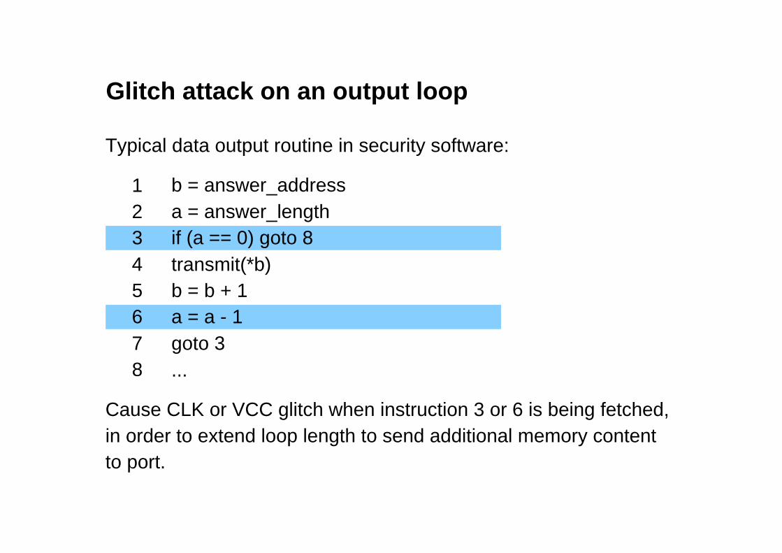
in order to extend loop length to send additional memory contentto port.
Cause CLK or VCC glitch when instruction 3 or 6 is being fetched,
3
54
67
1a = answer_length
a = a - 1b = b + 1
if (a == 0) goto 8
...
transmit(*b)
b = answer_address2
8goto 3
Glitch attack on an output loop
Typical data output routine in security software:

Instruction 1: CLR C Instruction 2: XOR B Instruction 3:
Data values appear in power profiles either as differential Hamming weights
Activation of EEPROM programming-voltage charge pump observable,
which allows to abort before state changes (e.g., with bad retry counters)
(~0.5-1 mA/bit) or as individual bits, e.g. with multiplication or shift instructions
Characteristic current spikes can identify executed instruction
EEPROM read-out amplifier, etc.)
Power Supply Current Forms a Significant Covert Channel
executed instruction sequence and observe cryptographic computations.
Record current in VCC/GND connection with 12-bit, 30-MHz ADC, in order to reconstruct
Current signature depends on accessed memory type (SRAM-write short circuit,
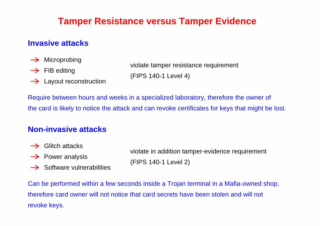
Microprobing
FIB editing
Layout reconstruction
Require between hours and weeks in a specialized laboratory, therefore the owner of
Glitch attacks
Power analysis
violate tamper resistance requirement
Invasive attacks
Non-invasive attacks
the card is likely to notice the attack and can revoke certificates for keys that might be lost.
revoke keys.
Tamper Resistance versus Tamper Evidence
(FIPS 140-1 Level 4)
(FIPS 140-1 Level 2)Software vulnerabilities
violate in addition tamper-evidence requirement
Can be performed within a few seconds inside a Trojan terminal in a Mafia-owned shop,
therefore card owner will not notice that card secrets have been stolen and will not

Classification of Attackers
Class I: Clever Outsiders. Often very intelligent, have insufficientknowledge of the system, have access to moderatelysophisticated equipment, use existing weaknesses in thesystem.
Class II: Knowledgeable Insiders.technical education and experience, varying degreesof understanding of the system but potential access to
Class III: Funded Organizations.
most relevant information, often highly sophisticated tools.
Teams of specialists with
Substantial specialized
complementary skills, great funding resources, capableof in-depth analysis and design of sophisticated attacks,most advanced tools, access to knowledgeable insiders.
[according to Abraham, Dolan, Double, Stevens: Transaction Security System,
IBM Systems Journal, Vol. 30, No. 2, 1991.]