hardware user’s manual - pudn.comread.pudn.com/downloads31/doc/101642/695_dev_bd.pdf · this...
TRANSCRIPT
eVAB-695
Hardware User’s Manual
Rad-Hard
Embedded Processor
Evaluation BoardTSC695
Rev.E - 22 March, 2001 1
eVAB-695
cumentssumesrights,
gratedtation
tion.
us:
.
Hardware User’s Manual Information
Foreword
Atmel Nantes S.A. reserves the right to make changes in the products or specifications contained in this doin order to improve design or performance and to supply the best possible products. Atmel Nantes S.A. also ano responsibility for the use of any circuits described herein, conveys no license under any patents or otherand makes no representations that the circuits are free from patent infringement. Applications for any intecircuits contained in this publication are for illustration purposes only and Atmel Nantes S.A. makes no represenor warranty that such applications will be suitable for the use specified without further testing or modificaReproduction of any portion hereof without the prior written consent of Atmel Nantes S.A. is prohibited.
Definition of Terms
The product Hardware User’s Manual contained in this document is referring to the following possible stat
Atmel Wireless & Microcontrollers on Line Information
World Wide Web: http://www.atmel-wm.com
Contact
Atmel Nantes S.A.La Chantrerie Route de Gachet,BP 7060244306 NANTES Cedex 03FranceTel: +33 2 40 18 18 18Fax: +33 2 40 18 19 20
Hardware User’s ManualIdentification
Definition
PreviewThis Hardware User’s Manual contains the targeted specifications, allelectrical parameters correspond to either targeted or simulated valuesSpecifications may change in any manner without notice.
Preliminary
This Hardware User’s Manual contains final functional specification. Theelectrical parameters given are based either on simulated values or onpreliminary product characterization results.Specifications may change in any manner without notice.
No Indication (blank)
This Hardware User’s Manual contains final specifications.Atmel Wireless & Microcontrollers reserves the right to make changes atany time, according to Atmel Wireless & Microcontrollers QualityAssurance procedures, in order to improve design and supply the bestpossible product.
2 Rev.E - 22 March, 2001
eVAB-695
7
7
7
.7
.7
.8
.8
8
8
.8
9
0
0
0
2
2
2
2
3
3
3
3
4
4
4
5
Table of Contents
INTRODUCTION . . . . . . . . . . . . . . . . . . . . . . . . . . . . . . . . . . . . . . . . . . . . . . . . . . . . . . . . . . . . .
Description. . . . . . . . . . . . . . . . . . . . . . . . . . . . . . . . . . . . . . . . . . . . . . . . . . . . . . . . . . . . . . . . . . . . .
Board Features. . . . . . . . . . . . . . . . . . . . . . . . . . . . . . . . . . . . . . . . . . . . . . . . . . . . . . . . . . . . . . . . . .
Processor. . . . . . . . . . . . . . . . . . . . . . . . . . . . . . . . . . . . . . . . . . . . . . . . . . . . . . . . . . . . . . . . . . . . . . . .
ROM . . . . . . . . . . . . . . . . . . . . . . . . . . . . . . . . . . . . . . . . . . . . . . . . . . . . . . . . . . . . . . . . . . . . . . . . . . .
RAM . . . . . . . . . . . . . . . . . . . . . . . . . . . . . . . . . . . . . . . . . . . . . . . . . . . . . . . . . . . . . . . . . . . . . . . . . . .
FPGA. . . . . . . . . . . . . . . . . . . . . . . . . . . . . . . . . . . . . . . . . . . . . . . . . . . . . . . . . . . . . . . . . . . . . . . . . . .
Expansion Connectors. . . . . . . . . . . . . . . . . . . . . . . . . . . . . . . . . . . . . . . . . . . . . . . . . . . . . . . . . . . . . . .
Debugging. . . . . . . . . . . . . . . . . . . . . . . . . . . . . . . . . . . . . . . . . . . . . . . . . . . . . . . . . . . . . . . . . . . . . . . .
Power. . . . . . . . . . . . . . . . . . . . . . . . . . . . . . . . . . . . . . . . . . . . . . . . . . . . . . . . . . . . . . . . . . . . . . . . . . .
Board Block Diagram. . . . . . . . . . . . . . . . . . . . . . . . . . . . . . . . . . . . . . . . . . . . . . . . . . . . . . . . . . . . .
PROCESSOR . . . . . . . . . . . . . . . . . . . . . . . . . . . . . . . . . . . . . . . . . . . . . . . . . . . . . . . . . . . . . . . 1
Processor Package. . . . . . . . . . . . . . . . . . . . . . . . . . . . . . . . . . . . . . . . . . . . . . . . . . . . . . . . . . . . . . . 1
Processor Pin-Out. . . . . . . . . . . . . . . . . . . . . . . . . . . . . . . . . . . . . . . . . . . . . . . . . . . . . . . . . . . . . . . 1
Processor Socket Part Number. . . . . . . . . . . . . . . . . . . . . . . . . . . . . . . . . . . . . . . . . . . . . . . . . . . . . 11
Emulation Capability. . . . . . . . . . . . . . . . . . . . . . . . . . . . . . . . . . . . . . . . . . . . . . . . . . . . . . . . . . . . 1
Debug Jumper. . . . . . . . . . . . . . . . . . . . . . . . . . . . . . . . . . . . . . . . . . . . . . . . . . . . . . . . . . . . . . . . . . 1
PROM8 Jumper. . . . . . . . . . . . . . . . . . . . . . . . . . . . . . . . . . . . . . . . . . . . . . . . . . . . . . . . . . . . . . . . 1
PARity Jumper. . . . . . . . . . . . . . . . . . . . . . . . . . . . . . . . . . . . . . . . . . . . . . . . . . . . . . . . . . . . . . . . . 1
ROM (or FLASH) . . . . . . . . . . . . . . . . . . . . . . . . . . . . . . . . . . . . . . . . . . . . . . . . . . . . . . . . . . . . 1
Flash 8-bit. . . . . . . . . . . . . . . . . . . . . . . . . . . . . . . . . . . . . . . . . . . . . . . . . . . . . . . . . . . . . . . . . . . . . 1
Flash 40-bit. . . . . . . . . . . . . . . . . . . . . . . . . . . . . . . . . . . . . . . . . . . . . . . . . . . . . . . . . . . . . . . . . . . . 1
Flash 8-bit / Flash 40-bit Selection. . . . . . . . . . . . . . . . . . . . . . . . . . . . . . . . . . . . . . . . . . . . . . . . . . 13
Schematic. . . . . . . . . . . . . . . . . . . . . . . . . . . . . . . . . . . . . . . . . . . . . . . . . . . . . . . . . . . . . . . . . . . . . . . .1
FlashCS Jumper. . . . . . . . . . . . . . . . . . . . . . . . . . . . . . . . . . . . . . . . . . . . . . . . . . . . . . . . . . . . . . . . . . .1
Flash 8-bit Write. . . . . . . . . . . . . . . . . . . . . . . . . . . . . . . . . . . . . . . . . . . . . . . . . . . . . . . . . . . . . . . . 1
Flash - Expansion SIMM. . . . . . . . . . . . . . . . . . . . . . . . . . . . . . . . . . . . . . . . . . . . . . . . . . . . . . . . . 1
Flash - Expansion SIMM selection. . . . . . . . . . . . . . . . . . . . . . . . . . . . . . . . . . . . . . . . . . . . . . . . . . . .14
Schematic. . . . . . . . . . . . . . . . . . . . . . . . . . . . . . . . . . . . . . . . . . . . . . . . . . . . . . . . . . . . . . . . . . . . . . . .1
Flash - Expansion SIMM pin-out. . . . . . . . . . . . . . . . . . . . . . . . . . . . . . . . . . . . . . . . . . . . . . . . . . . . .15
Rev.E - 22 March, 2001 3
eVAB-695
17
7
7
7
8
0
0
0
0
2
2
2
2
3
3
3
25
6
6
6
7
7
7
Example of Flash - Expansion SIMM. . . . . . . . . . . . . . . . . . . . . . . . . . . . . . . . . . . . . . . . . . . . . . . 15
RAM . . . . . . . . . . . . . . . . . . . . . . . . . . . . . . . . . . . . . . . . . . . . . . . . . . . . . . . . . . . . . . . . . . . . . . .
RAM - Bank 0. . . . . . . . . . . . . . . . . . . . . . . . . . . . . . . . . . . . . . . . . . . . . . . . . . . . . . . . . . . . . . . . . . 1
RAM - Bank 1. . . . . . . . . . . . . . . . . . . . . . . . . . . . . . . . . . . . . . . . . . . . . . . . . . . . . . . . . . . . . . . . . . 1
RAM - Expansion SIMM A. . . . . . . . . . . . . . . . . . . . . . . . . . . . . . . . . . . . . . . . . . . . . . . . . . . . . . . 1
RAM - Expansion SIMM A selection. . . . . . . . . . . . . . . . . . . . . . . . . . . . . . . . . . . . . . . . . . . . . . . . . 17
RAM - Expansion SIMM A pin-out. . . . . . . . . . . . . . . . . . . . . . . . . . . . . . . . . . . . . . . . . . . . . . . . . . . 17
RAM - Expansion SIMM B. . . . . . . . . . . . . . . . . . . . . . . . . . . . . . . . . . . . . . . . . . . . . . . . . . . . . . . 1
RAM - Expansion SIMM B selection. . . . . . . . . . . . . . . . . . . . . . . . . . . . . . . . . . . . . . . . . . . . . . . . . 18
RAM - Expansion SIMM B pin-out. . . . . . . . . . . . . . . . . . . . . . . . . . . . . . . . . . . . . . . . . . . . . . . . . . . 18
Example of RAM - Expansion SIMM. . . . . . . . . . . . . . . . . . . . . . . . . . . . . . . . . . . . . . . . . . . . . . . 19
FPGA . . . . . . . . . . . . . . . . . . . . . . . . . . . . . . . . . . . . . . . . . . . . . . . . . . . . . . . . . . . . . . . . . . . . . . 2
FPGA Part Number. . . . . . . . . . . . . . . . . . . . . . . . . . . . . . . . . . . . . . . . . . . . . . . . . . . . . . . . . . . . . . 2
FPGA Socket Part Number. . . . . . . . . . . . . . . . . . . . . . . . . . . . . . . . . . . . . . . . . . . . . . . . . . . . . . . . 2
FPGA Pin-out. . . . . . . . . . . . . . . . . . . . . . . . . . . . . . . . . . . . . . . . . . . . . . . . . . . . . . . . . . . . . . . . . . 2
FPGA Clocks. . . . . . . . . . . . . . . . . . . . . . . . . . . . . . . . . . . . . . . . . . . . . . . . . . . . . . . . . . . . . . . . . . 2
FPGA Clocks Schematic. . . . . . . . . . . . . . . . . . . . . . . . . . . . . . . . . . . . . . . . . . . . . . . . . . . . . . . . . . . 2
FPGA Clocks Jumper. . . . . . . . . . . . . . . . . . . . . . . . . . . . . . . . . . . . . . . . . . . . . . . . . . . . . . . . . . . . . . 2
FPGA External Clock. . . . . . . . . . . . . . . . . . . . . . . . . . . . . . . . . . . . . . . . . . . . . . . . . . . . . . . . . . . . . . 2
FPGA Downloading. . . . . . . . . . . . . . . . . . . . . . . . . . . . . . . . . . . . . . . . . . . . . . . . . . . . . . . . . . . . . 2
Serial PROM. . . . . . . . . . . . . . . . . . . . . . . . . . . . . . . . . . . . . . . . . . . . . . . . . . . . . . . . . . . . . . . . . . . . . 2
Bit-Blaster. . . . . . . . . . . . . . . . . . . . . . . . . . . . . . . . . . . . . . . . . . . . . . . . . . . . . . . . . . . . . . . . . . . . . . . 2
DMA . . . . . . . . . . . . . . . . . . . . . . . . . . . . . . . . . . . . . . . . . . . . . . . . . . . . . . . . . . . . . . . . . . . . . . .
TSC695 POWER & CLOCK . . . . . . . . . . . . . . . . . . . . . . . . . . . . . . . . . . . . . . . . . . . . . . . . . . . 2
TSC695 Power. . . . . . . . . . . . . . . . . . . . . . . . . . . . . . . . . . . . . . . . . . . . . . . . . . . . . . . . . . . . . . . . . 2
TSC695 Clocks. . . . . . . . . . . . . . . . . . . . . . . . . . . . . . . . . . . . . . . . . . . . . . . . . . . . . . . . . . . . . . . . . 2
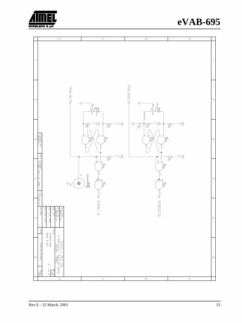
RESET, HALT, EWDINT & STATUS LED’s . . . . . . . . . . . . . . . . . . . . . . . . . . . . . . . . . . . . 27
RESET . . . . . . . . . . . . . . . . . . . . . . . . . . . . . . . . . . . . . . . . . . . . . . . . . . . . . . . . . . . . . . . . . . . . . . . 2
Schematic. . . . . . . . . . . . . . . . . . . . . . . . . . . . . . . . . . . . . . . . . . . . . . . . . . . . . . . . . . . . . . . . . . . . . . . 2
Push Button Location. . . . . . . . . . . . . . . . . . . . . . . . . . . . . . . . . . . . . . . . . . . . . . . . . . . . . . . . . . . . . . 2
4 Rev.E - 22 March, 2001
eVAB-6958
8
8
8
9
9
9
9
0
1
1
2
3
4
5
5
5
6
7
8
9
0
1
4
HALT . . . . . . . . . . . . . . . . . . . . . . . . . . . . . . . . . . . . . . . . . . . . . . . . . . . . . . . . . . . . . . . . . . . . . . . . 2
Schematic. . . . . . . . . . . . . . . . . . . . . . . . . . . . . . . . . . . . . . . . . . . . . . . . . . . . . . . . . . . . . . . . . . . . . . . .2
Push Button Location. . . . . . . . . . . . . . . . . . . . . . . . . . . . . . . . . . . . . . . . . . . . . . . . . . . . . . . . . . . . . . .2
SMB Connector Location. . . . . . . . . . . . . . . . . . . . . . . . . . . . . . . . . . . . . . . . . . . . . . . . . . . . . . . . . . .2
EWDINT. . . . . . . . . . . . . . . . . . . . . . . . . . . . . . . . . . . . . . . . . . . . . . . . . . . . . . . . . . . . . . . . . . . . . . 2
Status LED’s. . . . . . . . . . . . . . . . . . . . . . . . . . . . . . . . . . . . . . . . . . . . . . . . . . . . . . . . . . . . . . . . . . . 2
Schematic. . . . . . . . . . . . . . . . . . . . . . . . . . . . . . . . . . . . . . . . . . . . . . . . . . . . . . . . . . . . . . . . . . . . . . . .2
LED’s Location. . . . . . . . . . . . . . . . . . . . . . . . . . . . . . . . . . . . . . . . . . . . . . . . . . . . . . . . . . . . . . . . . . .2
TEST POINTS. . . . . . . . . . . . . . . . . . . . . . . . . . . . . . . . . . . . . . . . . . . . . . . . . . . . . . . . . . . . . . . 3
LOGIC ANALIZER POD’s . . . . . . . . . . . . . . . . . . . . . . . . . . . . . . . . . . . . . . . . . . . . . . . . . . . . 3
POD 1. . . . . . . . . . . . . . . . . . . . . . . . . . . . . . . . . . . . . . . . . . . . . . . . . . . . . . . . . . . . . . . . . . . . . . . . 3
POD 2. . . . . . . . . . . . . . . . . . . . . . . . . . . . . . . . . . . . . . . . . . . . . . . . . . . . . . . . . . . . . . . . . . . . . . . . 3
POD 3. . . . . . . . . . . . . . . . . . . . . . . . . . . . . . . . . . . . . . . . . . . . . . . . . . . . . . . . . . . . . . . . . . . . . . . . 3
POD 4. . . . . . . . . . . . . . . . . . . . . . . . . . . . . . . . . . . . . . . . . . . . . . . . . . . . . . . . . . . . . . . . . . . . . . . . 3
SERIAL LINKS . . . . . . . . . . . . . . . . . . . . . . . . . . . . . . . . . . . . . . . . . . . . . . . . . . . . . . . . . . . . . . 3
Serial A. . . . . . . . . . . . . . . . . . . . . . . . . . . . . . . . . . . . . . . . . . . . . . . . . . . . . . . . . . . . . . . . . . . . . . . 3
Serial B. . . . . . . . . . . . . . . . . . . . . . . . . . . . . . . . . . . . . . . . . . . . . . . . . . . . . . . . . . . . . . . . . . . . . . . 3
SUN Connection. . . . . . . . . . . . . . . . . . . . . . . . . . . . . . . . . . . . . . . . . . . . . . . . . . . . . . . . . . . . . . . . 3
PC Connection. . . . . . . . . . . . . . . . . . . . . . . . . . . . . . . . . . . . . . . . . . . . . . . . . . . . . . . . . . . . . . . . . 3
TAP CONNECTOR . . . . . . . . . . . . . . . . . . . . . . . . . . . . . . . . . . . . . . . . . . . . . . . . . . . . . . . . . . 3
EXPANSION CONNECTORS . . . . . . . . . . . . . . . . . . . . . . . . . . . . . . . . . . . . . . . . . . . . . . . . . 39
3 x 32 points connector - P1. . . . . . . . . . . . . . . . . . . . . . . . . . . . . . . . . . . . . . . . . . . . . . . . . . . . . . . 3
3 x 32 points connector - P2. . . . . . . . . . . . . . . . . . . . . . . . . . . . . . . . . . . . . . . . . . . . . . . . . . . . . . . 4
3 x 32 points connector - P3. . . . . . . . . . . . . . . . . . . . . . . . . . . . . . . . . . . . . . . . . . . . . . . . . . . . . . . 4
BOARD IMPLEMENTATION . . . . . . . . . . . . . . . . . . . . . . . . . . . . . . . . . . . . . . . . . . . . . . . . . 42
DEVIATIONS . . . . . . . . . . . . . . . . . . . . . . . . . . . . . . . . . . . . . . . . . . . . . . . . . . . . . . . . . . . . . . . 4
Rev.E - 22 March, 2001 5
eVAB-6954
4
5
CB[6:0] and DPAR on FPGA. . . . . . . . . . . . . . . . . . . . . . . . . . . . . . . . . . . . . . . . . . . . . . . . . . . . . . 4
RESET and HALT driven by JTAG connector. . . . . . . . . . . . . . . . . . . . . . . . . . . . . . . . . . . . . . . . 44
TSC695 Signals on FPGA. . . . . . . . . . . . . . . . . . . . . . . . . . . . . . . . . . . . . . . . . . . . . . . . . . . . . . . . 4
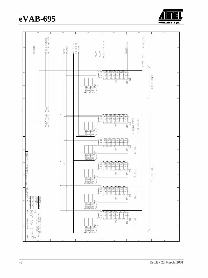
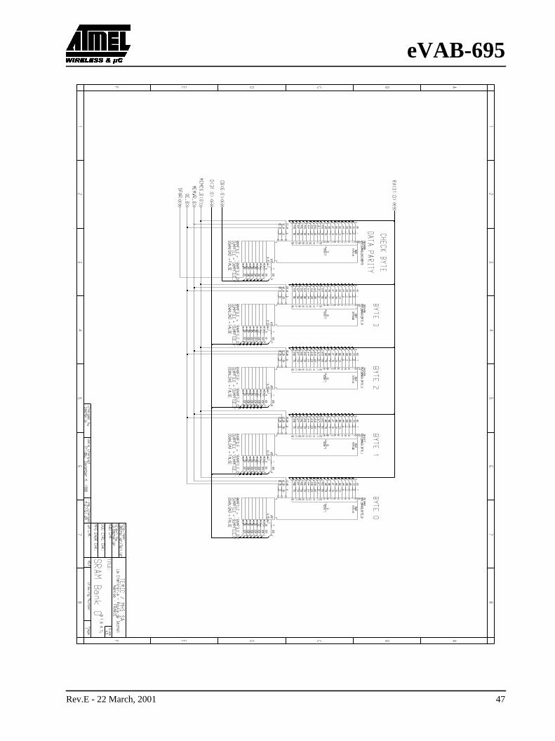
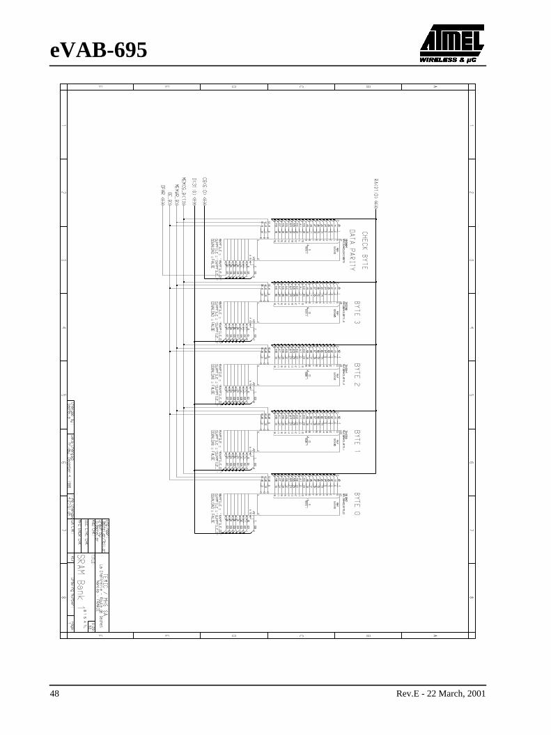
SCHEMATICS . . . . . . . . . . . . . . . . . . . . . . . . . . . . . . . . . . . . . . . . . . . . . . . . . . . . . . . . . . . . . . 4
6 Rev.E - 22 March, 2001
eVAB-695
menting
MArruptl busesbugger
luationn
6.3
) of the
bytes
gger.
<Title_Page2>
1. INTRODUCTION
1.1. Description
The eVAB-695 is a board used to evaluate and demonstrate the new 32-bit RISC Embedded processor implethe SPARC architecture V7 specification, the TSC695.
The TSC695 includes on chip an Integer Unit (IU), a Floating Point Unit (FPU), a Memory Controller and a DArbiter. For Real Time applications, the TSC695 offers a high security Watch Dog, two Timer’s, an InteController, Parallel and Serial interfaces. Fault tolerance is supported using specific parity on internal/externaand an EDAC on the external data bus. The design is highly testable with the support of an On-Chip De(OCD), an internal and boundary scan through JTAG interface.
This board is based on the TSC695, a ROM space, a SRAM space, a DPRAM space and a FPGA50k witch integratessome functions for DMA accesses, logic glue, custom peripherals, ...
Several extension connectors and a large range of memory mapping produces an high flexibility to the evaor the demonstration. A free user connection linked to the FPGA50k is also proposed to customize the applicatiointerfaces.
1.2. Board Features
The eVAB-695 board is designed in standard VME. It is a board in B / 2U format (23.3 x 16 cm or 9.2 xinches). The rear and front 96-pin connectors only respect the power lines of the VME bus.
1.2.1. Processor
The TSC695 includes all the major features (except co-processor implementation and master/checker modeERC32 chip-set. The component can divided in sic blocks:
• the IU based on SPARC V7.0 architecture,
• the FPU compliant to ANSI/IEEE 754 standard,
• a specific memory controller,
• a slave DMA arbiter,
• seven peripherals:
• 1 watchdog (or NMI),
• 2 timers,
• 1 interrupt controller,
• 1 GPI,
• 2 UART’s,
• a JTAG controller with OCD
1.2.2. ROM
The eVAB-695 can have either a 8-bit boot-flash for 512 Kbytes of code either a 40-bit boot-flash for 2 Mof code.
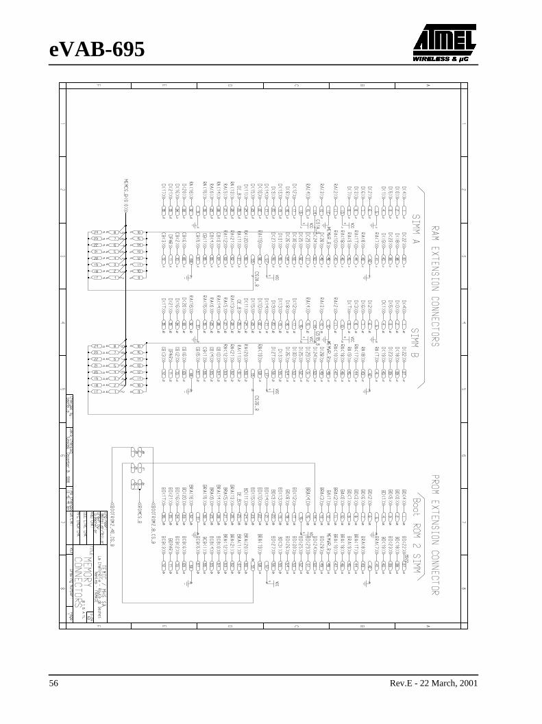
Up to 4M bytes of code using one SIMM module can be mounted as ROM expansion.
The eVAB-695 is equipped either with SPARCmon, a stand-alone monitor, either with RDBmon, a remote debu
Rev.E - 22 March, 2001 7
eVAB-695
s andted to the
n, DMA,
m the
1.2.3. RAM
The eVAB-695 have 2 banks of 40-bit SRAM for 2 Mbytes of data/code each.
Up to 8M bytes of data/code using 2 SIMM modules can be mounted as RAM expansion.
1.2.4. FPGA
An ALTERA 10K50 FPGA is mounted on board. It receives all signals of the TSC695 except for the addresdata buses. The FPGA receives the address and data buffered buses. Some other FPGA I/O’s are connecexpansion connectors.
The FPGA is downloaded via either a serial PROM, either via the Bit-Blaster connector.
The board can run without the FPGA.
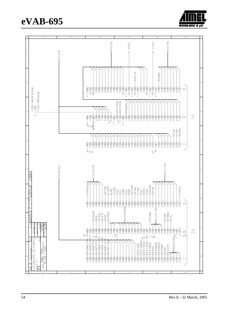
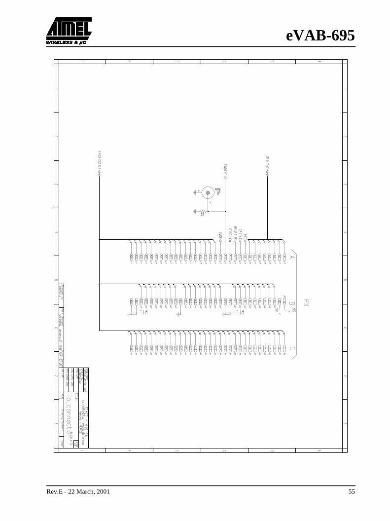
1.2.5. Expansion Connectors
3 expansion connectors are provided. P1 and P2 are reserved for system expansion (processor emulatioexchange RAM, ...) and P3 is dedicated for I/O expansion.
1.2.6. Debugging
• 1 connector TAP-JTAG for hardware debugging.
• 4 x 34-bit pods for logic analysis.
• 32 couples of signal/Gnd for test points.
• system halt input.
• NMI input (c.f EWDINT)
1.2.7. Power
The eVAB-695 can be powered (Vcc board) in 5 or 3.3 volts with a proper choice of components.
Each of the TSC695 Vcc core (VccI) and the TSC695 Vcc buffers (VccO) can be powered separately froVcc board.
8 Rev.E - 22 March, 2001
eVAB-695
t.
on the
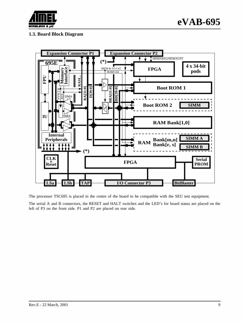
1.3. Board Block Diagram
The processor TSC695 is placed in the centre of the board to be compatible with the SEU test equipmen
The serial A and B connectors, the RESET and HALT switches and the LED’s for board status are placedleft of P3 on the front side. P1 and P2 are placed on rear side.
ALE
SY
SC
LK
DMA
DMA
InternalPeripherals
695E
FP
U
IU
RA
[31:
0] Boot ROM 1
Boot ROM 2 SIMM
RAM
RAM Bank[1,0]
SIMM A
SIMM B
Bank[m,n]Bank[r, s]
RAM CtrlMEM & I/O Ctrl
FPGA
LSa LSb TAP I/O Connector P3
4 x 34-bitpods
CLK
BD
[39:
0]
BR
A[3
1:0]
D[3
9:0]
&Reset
Expansion Connector P1 Expansion Connector P2MDMAREQ/MDMAGNT
Mem
ory
Inte
rfac
e
RA
SI..
.
FPGA
(*)
(*)
BitBlaster
SerialPROM
Rev.E - 22 March, 2001 9
eVAB-695
QFP-Fbottommoved
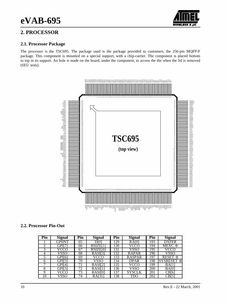
2. PROCESSOR
2.1. Processor Package
The processor is the TSC695. The package used is the package provided to customers, the 256-pin Mpackage. This component is mounted on a special support, with a chip-carrier. The component is placedto top in its support. An hole is made on the board, under the component, to access the die when the lid is re(SEU tests).
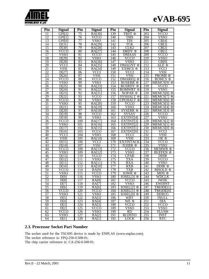
2.2. Processor Pin-Out
Pin Signal Pin Signal Pin Signal Pin Signal1 GPIINT 65 D[0] 129 RA[0] 193 DXFER2 GPI[7] 66 RSIZE[1] 130 VCCO 194 MEXC3 VCCO 67 RSIZE[0] 131 VSSO 195 VCCO4 VSSO 68 RASI[3] 132 RAPAR 196 VSSO5 GPI[6] 69 VCCO 133 RASPAR 197 RESET6 GPI[5] 70 VSSO 134 DPAR 198 SYSRESET7 GPI[4] 71 RASI[2] 135 VCCO 199 BA[1]8 GPI[3] 72 RASI[1] 136 VSSO 200 BA[0]9 VCCO 73 RASI[0] 137 SYSCLK 201 CB[6]10 VSSO 74 RA[31] 138 TDO 202 CB[5]
1 2 3 4 5 6 7 8 9 10 11 12 13 14 15 16 17 18 19 20 21 22 23 24 25 26 27 28 29 30 31 32 33 34 35 36 37 38 39 40 41 42 43 44 45 46 47 48 49 50 51 52 53 54 55 56 57 58 59 60 61 62 63 64
256255254253252251250249248247246245244243242241240239238237236235234233232231230229228227226225224223222221220219218217216215214213212211210209208207206205204203202201200199198197196195194193
6566676869707172737475767778798081828384858687888990919293949596979899
100101102103104105106107108109110111112113114115116117118119120121122123124125126127128
192
191
190
189
188
187
186
185
184
183
182
181
180
179
178
177
176
175
174
173
172
171
170
169
168
167
166
165
164
163
162
161
160
159
158
157
156
155
154
153
152
151
150
149
148
147
146
145
144
143
142
141
140
139
138
137
136
135
134
133
132
131
130
129
GP
INT
GP
I[7]
VC
CO
VS
SO
GP
I[6]
GP
I[5]
GP
I[4]
GP
I[3]
VC
CO
VS
SO
GP
I[2]
GP
I[1]
GP
I[0]
D[3
1]D
[30]
VC
CO
VS
SO
D[2
9]D
[28]
VC
CI
VS
SI
D[2
7]D
[26]
VC
CO
VS
SO
D[2
5]D
[24]
D[2
3]D
[22]
VC
CO
VS
SO
D[2
1]D
[20]
D[1
9]D
[18]
VC
CO
VS
SO
D[1
7]D
[16]
VC
CI
VS
SI
D[1
5]D
[14]
VC
CO
VS
SO
D[1
3]D
[12]
D[1
1]D
[10]
VC
CO
VS
SO
D[9
]D
[8]
D[7
]D
[6]
VC
CO
VS
SO
D[5
]D
[4]
D[3
]D
[2]
VC
CO
VS
SO
D[1
]
RSIZE[1]RSIZE[0]RASI[3]VCCOVSSORASI[2]RASI[1]RASI[0]RA[31]RA[30]VCCOVSSORA[29]RA[28]RA[27]VCCOVSSORA[26]RA[25]RA[24]VCCIVSSIVCCOVSSORA[23]RA[22]RA[21]VCCOVSSORA[20]RA[19]RA[18]VCCOVSSORA[17]RA[16]RA[15]VCCOVSSORA[14]VCCIVSSIRA[13]RA[12]VCCOVSSORA[11]RA[10]RA[9]VCCOVSSORA[8]RA[7]RA[6]VCCOVSSORA[5]RA[4]RA[3]VCCOVSSORA[2]RA[1]
LOC
KR
LDS
TO RD
VS
SO
VC
CO
WE
WR
TIO
SE
L[0]
IOS
EL[
1]IO
SE
L[2]
VS
SO
VC
CO
IOS
EL[
3]IO
WR
TxB
RxB
RxA
TxA
CP
AR
VS
SO
VC
CO
IUE
RR
EX
TIN
TAC
KV
SS
IV
CC
IE
XTI
NT[
0]E
XTI
NT[
1]E
XTI
NT[
2]E
XTI
NT[
3]E
XTI
NT[
4]S
YS
AV
SY
SE
RR
VS
SO
VC
CO
CP
UH
ALT
SY
SH
ALT
NO
PA
RR
OM
WR
TB
US
RD
YB
US
ER
RD
MA
RE
QV
SS
IV
CC
IE
XM
CS
DM
AG
NT
VS
SO
VC
CO
DM
AA
SD
RD
YC
LK2
TCK
TDI
TMS
TRS
TTD
OS
YS
CLK
VS
SO
VC
CO
DP
AR
RA
SP
AR
RA
PA
RV
SS
OV
CC
OR
A[0
]
RTCINST
FLUSHVSSOVCCO
DIAINULL
DEBUGTMODE[0]TMODE[1]
EWDINTIWDE
WDCLKMDS
MHOLDDDIRVSSOVCCODDIR
BUFFENMEMWR
VSSOVCCO
OEVSSIVCCI
MEMCS[0]MEMCS[1]MEMCS[2]
VSSOVCCO
MEMCS[3]MEMCS[4]MEMCS[5]MEMCS[6]MEMCS[7]MEMCS[8]
VSSOVCCO
MEMCS[9]ROMCSPROM8
VSSIVCCIALE
CB[0]VSSOVCCOCB[1]CB[2]CB[3]CB[4]VSSOVCCOCB[5]CB[6]BA[0]BA[1]
SYSRESETRESETVSSOVCCOMEXC
DXFER
TSC695(top view)
10 Rev.E - 22 March, 2001
eVAB-695
2.3. Processor Socket Part Number
The socket used for the TSC695 device is made by ENPLAS (www.enplas.com).The socket reference is: FPQ-256-0.508-01.The chip carrier reference is: CA-256-0.508-01.
11 GPI[2] 75 RA[30] 139 TRST 203 VCCO12 GPI[1] 76 VCCO 140 TMS 204 VSSO13 GPI[0] 77 VSSO 141 TDI 205 CB[4]14 D[31] 78 RA[29] 142 TCK 206 CB[3]15 D[30] 79 RA[28] 143 CLK2 207 CB[2]16 VCCO 80 RA[27] 144 DRDY 208 CB[1]17 VSSO 81 VCCO 145 DMAAS 209 VCCO18 D[29] 82 VSSO 146 VCCO 210 VSSO19 D[28] 83 RA[26] 147 VSSO 211 CB[0]20 VCCI 84 RA[25] 148 DMAGNT 212 ALE 21 VSSI 85 RA[24] 149 EXMCS 213 VCCI22 D[27] 86 VCCI 150 VCCI 214 VSSI23 D[26] 87 VSSI 151 VSSI 215 PROM824 VCCO 88 VCCO 152 DMAREQ 216 ROMCS25 VSSO 89 VSSO 153 BUSERR 217 MEMCS[9] 26 D[25] 90 RA[23] 154 BUSRDY 218 VCCO27 D[24] 91 RA[22] 155 ROMWRT 219 VSSO28 D[23] 92 RA[21] 156 NOPAR 220 MEMCS[8] 29 D[22] 93 VCCO 157 SYSHALT 221 MEMCS[7] 30 VCCO 94 VSSO 158 CPUHALT 222 MEMCS[6] 31 VSSO 95 RA[20] 159 VCCO 223 MEMCS[5]32 D[21] 96 RA[19] 160 VSSO 224 MEMCS[4]33 D[20] 97 RA[18] 161 SYSERR 225 MEMCS[3] 34 D[19] 98 VCCO 162 SYSAV 226 VCCO35 D[18] 99 VSSO 163 EXTINT[4] 227 VSSO36 VCCO 100 RA[17] 164 EXTINT[3] 228 MEMCS[2]37 VSSO 101 RA[16] 165 EXTINT[2] 229 MEMCS[1]38 D[17] 102 RA[15] 166 EXTINT[1] 230 MEMCS[0]39 D[16] 103 VCCO 167 EXTINT[0] 231 VCCI40 VCCI 104 VSSO 168 VCCI 232 VSSI41 VSSI 105 RA[14] 169 VSSI 233 OE42 D[15] 106 VCCI 170 EXTINTACK 234 VCCO43 D[14] 107 VSSI 171 IUERR 235 VSSO44 VCCO 108 RA[13] 172 VCCO 236 MEMWR45 VSSO 109 RA[12] 173 VSSO 237 BUFFEN46 D[13] 110 VCCO 174 CPAR 238 DDIR47 D[12] 111 VSSO 175 TXA 239 VCCO48 D[11] 112 RA[11] 176 RXA 240 VSSO49 D[10] 113 RA[10] 177 RXB 241 DDIR50 VCCO 114 RA[9] 178 TXB 242 MHOLD51 VSSO 115 VCCO 179 IOWR 243 MDS 52 D[9] 116 VSSO 180 IOSEL[3] 244 WDCLK53 D[8] 117 RA[8] 181 VCCO 245 IWDE54 D[7] 118 RA[7] 182 VSSO 246 EWDINT55 D[6] 119 RA[6] 183 IOSEL[2] 247 TMODE[1]56 VCCO 120 VCCO 184 IOSEL[1] 248 TMODE[0]57 VSSO 121 VSSO 185 IOSEL[0] 249 DEBUG58 D[5] 122 RA[5] 186 WRT 250 INULL59 D[4] 123 RA[4] 187 WE 251 DIA60 D[3] 124 RA[3] 188 VCCO 252 VCCO61 D[2] 125 VCCO 189 VSSO 253 VSSO62 VCCO 126 VSSO 190 RD 254 FLUSH63 VSSO 127 RA[2] 191 RLDSTO 255 INST64 D[1] 128 RA[1] 192 LOCK 256 RTC
Pin Signal Pin Signal Pin Signal Pin Signal
Rev.E - 22 March, 2001 11
eVAB-695
leP1 &
2.4. Emulation Capability
Excepted for TMODE[1,0], DEBUG, ROMWRT, NOPAR and JTAG port, all TSC695 signals are availabon P1 & P2 connectors. In this way, an emulation of the processor (support empty) can be done throughP2 (ex: MCM or ERC32 chip-set).
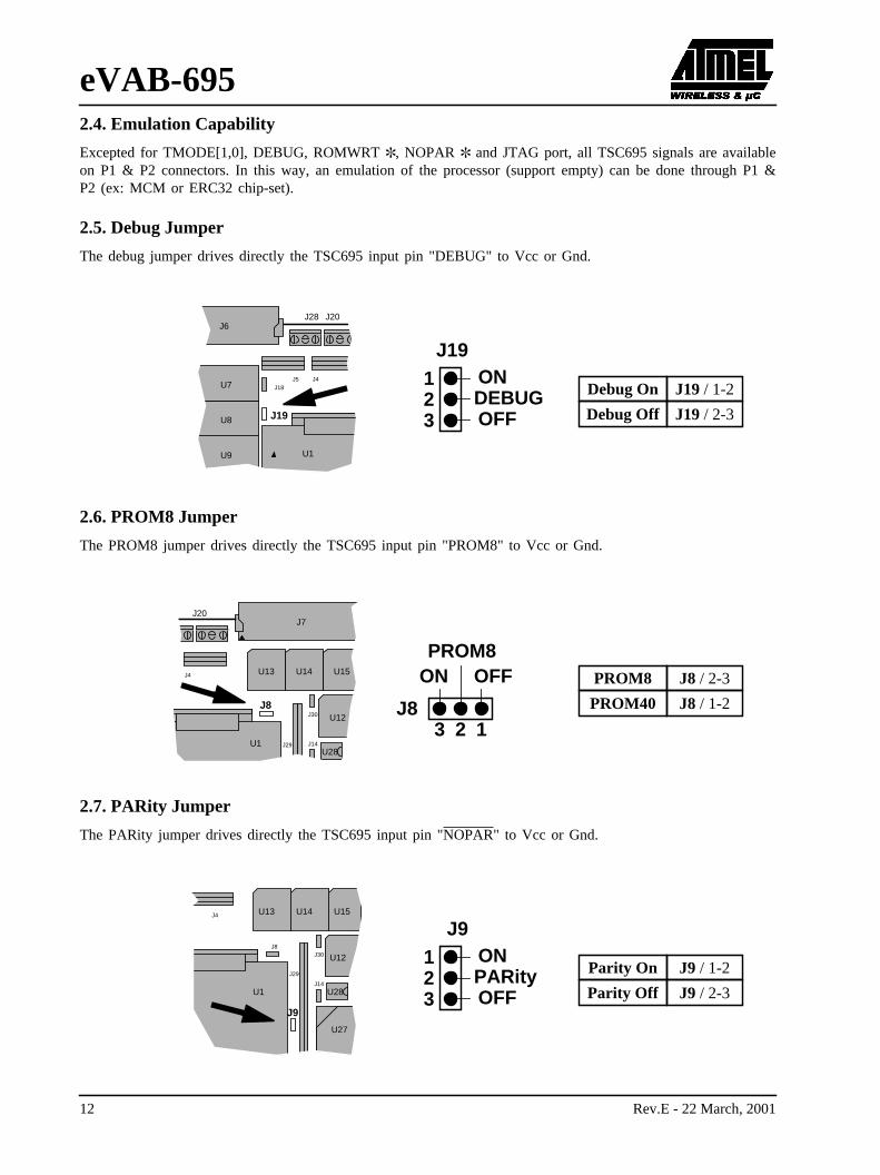
2.5. Debug Jumper
The debug jumper drives directly the TSC695 input pin "DEBUG" to Vcc or Gnd.
2.6. PROM8 Jumper
The PROM8 jumper drives directly the TSC695 input pin "PROM8" to Vcc or Gnd.
2.7. PARity Jumper
The PARity jumper drives directly the TSC695 input pin "NOPAR" to Vcc or Gnd.
J6
U1
U7
U8
U9
J28
J5 J4
J19
J18
J19
DEBUGON
OFF
123 J19 / 2-3
J19 / 1-2
Debug Off
Debug On
J20
J8
PROM8ON OFF
123J8 / 1-2
J8 / 2-3
PROM40
PROM8
U12
J7
U1U28
J8
J29
J30
J14
U15U14U13
J20
J4
J9
PARityON
OFF
123 J9 / 2-3
J9 / 1-2
Parity Off
Parity OnU12
U1
U27
U28
J8
J9
J29
J30
J14
U15U14U13J4
12 Rev.E - 22 March, 2001
eVAB-695
pacity
3.3V in
check0
ly the
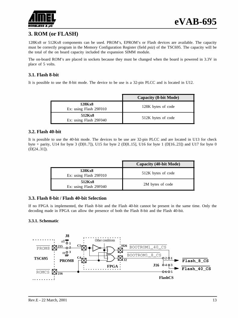
3. ROM (or FLASH)
128Kx8 or 512Kx8 components can be used. PROM’s, EPROM’s or Flash devices are available. The camust be correctly program in the Memory Configuration Register (fieldpsiz) of the TSC695. The capacity will bethe total of the on board capacity included the expansion SIMM module.
The on-board ROM’s are placed in sockets because they must be changed when the board is powered inplace of 5 volts.
3.1. Flash 8-bit
It is possible to use the 8-bit mode. The device to be use is a 32-pin PLCC and is located in U12.
3.2. Flash 40-bit
It is possible to use the 40-bit mode. The devices to be use are 32-pin PLCC and are located in U13 forbyte + parity, U14 for byte 3 (D[0..7]), U15 for byte 2 (D[8..15], U16 for byte 1 (D[16..23]) and U17 for byte(D[24..31]).
3.3. Flash 8-bit / Flash 40-bit Selection
If no FPGA is implemented, the Flash 8-bit and the Flash 40-bit cannot be present in the same time. Ondecoding made in FPGA can allow the presence of both the Flash 8-bit and the Flash 40-bit.
3.3.1. Schematic
Capacity (8-bit Mode)
128Kx8Ex: using Flash 29F010
128K bytes of code
512Kx8Ex: using Flash 29F040
512K bytes of code
Capacity (40-bit Mode)
128Kx8Ex: using Flash 29F010
512K bytes of code
512Kx8Ex: using Flash 29F040
2M bytes of code
ROMCS
PROM8
TSC695
J8
PROM8FPGA
BOOTROM1_40_CS
BOOTROM1_8_CSFlash_8_CS
Flash_40_CSJ16
FlashCS
12
34
56
Other conditions
216
215
C4
C5 H26
J2
123on
off
Rev.E - 22 March, 2001 13
eVAB-695
ROM)
in the
r thend the
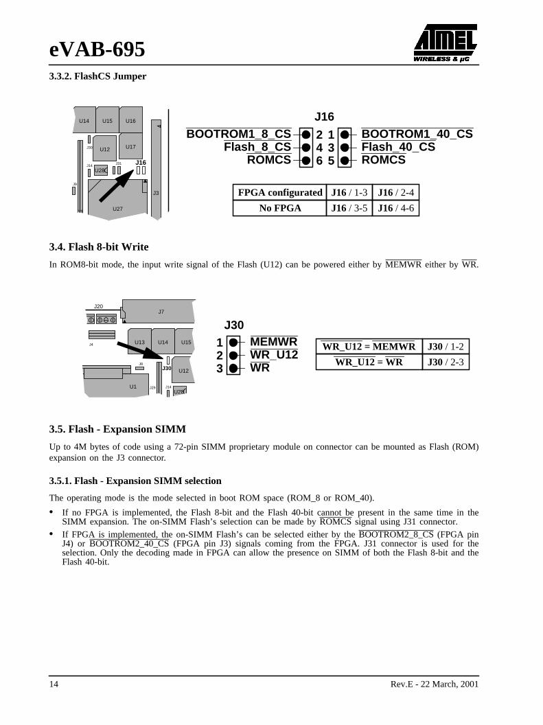
3.3.2. FlashCS Jumper
3.4. Flash 8-bit Write
In ROM8-bit mode, the input write signal of the Flash (U12) can be powered either byMEMWR either byWR.
3.5. Flash - Expansion SIMM
Up to 4M bytes of code using a 72-pin SIMM proprietary module on connector can be mounted as Flash (expansion on the J3 connector.
3.5.1. Flash - Expansion SIMM selection
The operating mode is the mode selected in boot ROM space (ROM_8 or ROM_40).
• If no FPGA is implemented, the Flash 8-bit and the Flash 40-bit cannot be present in the same timeSIMM expansion. The on-SIMM Flash’s selection can be made byROMCS signal using J31 connector.
• If FPGA is implemented, the on-SIMM Flash’s can be selected either by theBOOTROM2_8_CS (FPGA pinJ4) or BOOTROM2_40_CS (FPGA pin J3) signals coming from the FPGA. J31 connector is used foselection. Only the decoding made in FPGA can allow the presence on SIMM of both the Flash 8-bit aFlash 40-bit.
J16
Flash_40_CSBOOTROM1_40_CS
ROMCS
135
J16 / 3-5
J16 / 1-3
No FPGA
FPGA configurated
U12
J3
U27
U28
J9
J30
J14J16
U17
U16U15U14
J29
246
Flash_8_CSBOOTROM1_8_CS
ROMCS
J16 / 4-6
J16 / 2-4
J31
J30 / 2-3
J30 / 1-2
WR_U12 = WR
WR_U12 = MEMWR
U12
J7
U1U28
J8
J29
J30
J14
U15U14U13
J20
J4
J30
WR_U12MEMWR
WR
123
14 Rev.E - 22 March, 2001
eVAB-695
bytes
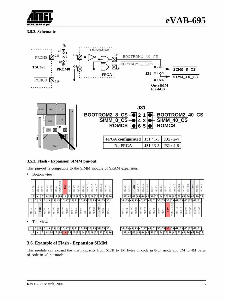
3.5.2. Schematic
3.5.3. Flash - Expansion SIMM pin-out
This pin-out is compatible to the SIMM module of SRAM expansion.
• Bottom view:
• Top view:
3.6. Example of Flash - Expansion SIMM
This module can expand the Flash capacity from 512K to 1M bytes of code in 8-bit mode and 2M to 4Mof code in 40-bit mode.
ROMCS
PROM8
TSC695
J8
PROM8FPGA
BOOTROM2_40_CS
BOOTROM2_8_CSSIMM_8_CS
SIMM_40_CSJ31
On-SIMM
12
34
56
Other conditions
216
215
C4
C5 J3
J4
123on
off
FlashCS
J31
SIMM_40_CSBOOTROM2_40_CS
ROMCS
135
J31 / 3-5
J31 / 1-3
No FPGA
FPGA configurated
U12
J3
U27
U28
J9
J30
J14J16
U17
U16U15U14
J29
246
SIMM_8_CSBOOTROM2_8_CS
ROMCS
J31 / 4-6
J31 / 2-4
J31
1
2
3
GN
D
5 7
BD
08
9
BD
09
11
BD
10
13
BD
11
15
4 6
BD
00
8
BD
01
10
BD
02
12
BD
03
14
+5
V
16
BA
00
18
BA
01
20 22
BC
B0
4
24
BC
B0
5
26B
CB
06
28B
CB
0730
ME
MW
R
32
BR
A1
9
34 36
BR
A0
2
17
BR
A0
3
19
BR
A0
4
21
BD
12
23
BD
13
25
BD
14
27
BD
15
29
GN
D
31 33 35 37
38
BR
A1
0
39
OE
41
BD
20
43
BD
21
45
BD
22
47
BD
23
49
BR
A0
7
51
40
GN
D
42
BD
16
44
BD
17
46
BD
18
48
BD
19
50
BR
A1
3
52
BR
A1
4
54
BR
A1
5
56
BR
A1
6
58
BD
24
60
BD
25
62
BD
26
64
BD
27
66
GN
D
68
BR
A2
0
70 72
BR
A0
8
53
BR
A0
9
55
+5
V
57 59
BD
28
61
BD
29
63
BD
30
65
BD
31
67
BR
A1
1
69 71
BR
A1
2
BR
A1
7
BR
A1
8
BR
A2
1
BC
B0
0
BC
B0
1
BC
B0
2
BC
B0
3
BD
04
BD
05
BD
06
BD
07
BR
A0
5
BR
A0
6
SIM
M_8
_CS
SIM
M_4
0_C
S
1
2
3 5 7 9 11 13 15
4 6 8 10 12 14 16 18 20 22 24 26 28 30 32 34 36
17 19 21 23 25 27 29 31 33 35 37
38
39 41 43 45 47 49 51
40 42 44 46 48 50 52 54 56 58 60 62 64 66 68 70 72
53 55 57 59 61 63 65 67 69 71
Rev.E - 22 March, 2001 15
eVAB-695
BRA[20:2]
BD[7:0] BD[15:8] BD[23:16] BD[31:24] BCB[7:0]
BA[1:0]BRA[18:2]
MEMWROE
0
123
AB
SIMM_8_CS
BRA[19]BRA[20]
GSIMM_40_CS
BRA[21]
FL
AS
H
(51
2K
x8)
FL
AS
H
(51
2K
x8)
FL
AS
H
(51
2K
x8)
FL
AS
H
(51
2K
x8)
FL
AS
H
(51
2K
x8)
FL
AS
H
(51
2K
x8)
13
91 /2
0
123
AB
G
13
91 /2
16 Rev.E - 22 March, 2001
eVAB-695
SIMM
3.3V in
, U5
U10
n the
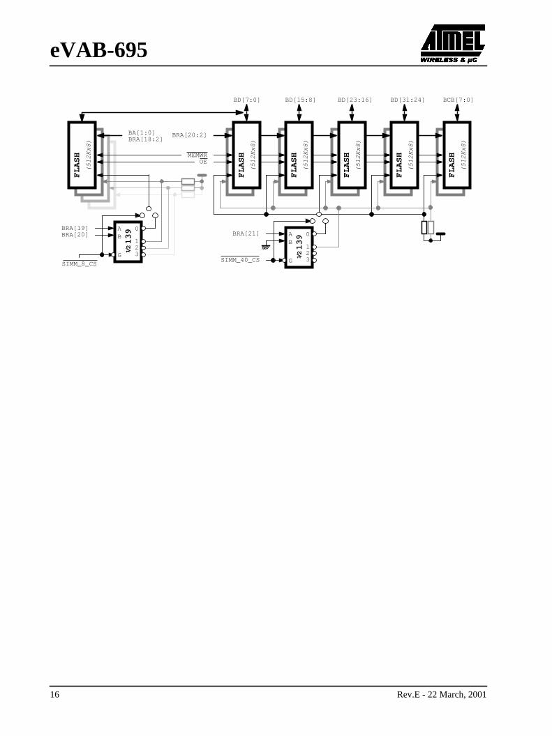
4. RAM
The RAM space (in 40-bit mode) is built in banks of 2M bytes of code/data.The two first banks are implemented on board, the other ones (up to 4) can implemented on two 72-pinmodules as RAM expansion.
The on-board RAM’s are placed in sockets because they must be changed when the board is powered inplace of 5 volts.
4.1. RAM - Bank 0
The first bank (Bank 0) is composed of five 512Kx8 SRAM’s selected byMEMCS[0] of the TSC695. These 5components, in 36-pin SOJ package, can be plugged in socket with the same footprint than the SRAM.The total capacity is 2M bytes of code/data.The devices used are located in U2 for check byte + parity, U3 for byte 3 (D[0..7]), U4 for byte 2 (D[8..15]for byte 1 (D[16..23]) and U6 for byte 0 (D[24..31]).
• First word address: 0x02000000
• Last word address: 0x021FFFFC
4.2. RAM - Bank 1
The second bank (Bank 1) is composed of five 512Kx8 SRAM’s selected byMEMCS[1] of the TSC695. These5 components, in 36-pin SOJ package, can be plugged in socket with the same footprint than the SRAM.The total capacity is 2M bytes of code/data.The devices used are located in U7 for check byte + parity, U8 for byte 3 (D[0..7]), U9 for byte 2 (D[8..15],for byte 1 (D[16..23]) and U11 for byte 0 (D[24..31]).
• First word address: 0x02200000
• Last word address: 0x023FFFFC
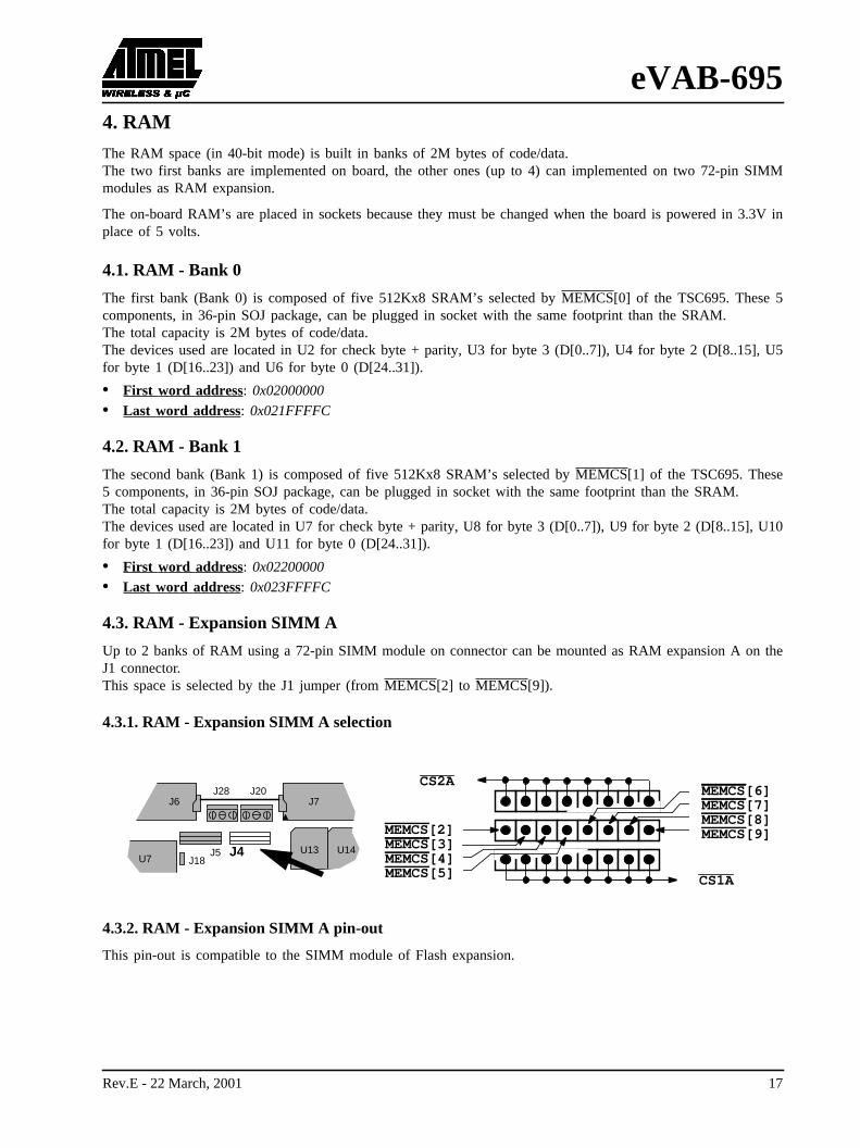
4.3. RAM - Expansion SIMM A
Up to 2 banks of RAM using a 72-pin SIMM module on connector can be mounted as RAM expansion A oJ1 connector.This space is selected by the J1 jumper (fromMEMCS[2] to MEMCS[9]).
4.3.1. RAM - Expansion SIMM A selection
4.3.2. RAM - Expansion SIMM A pin-out
This pin-out is compatible to the SIMM module of Flash expansion.
CS2A
CS1A
MEMCS[2]
MEMCS[6]J7J6
U7U14U13
J28
J5 J4J18
MEMCS[3]MEMCS[4]MEMCS[5]
MEMCS[7]MEMCS[8]MEMCS[9]
J20
Rev.E - 22 March, 2001 17
eVAB-695
n the
• Bottom view:
• Top view:
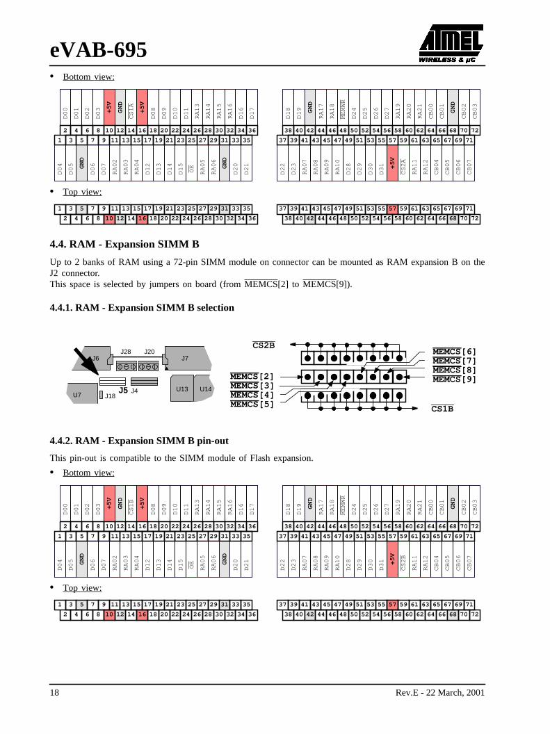
4.4. RAM - Expansion SIMM B
Up to 2 banks of RAM using a 72-pin SIMM module on connector can be mounted as RAM expansion B oJ2 connector.This space is selected by jumpers on board (fromMEMCS[2] to MEMCS[9]).
4.4.1. RAM - Expansion SIMM B selection
4.4.2. RAM - Expansion SIMM B pin-out
This pin-out is compatible to the SIMM module of Flash expansion.
• Bottom view:
• Top view:
GN
D
+5
V
1
2
3
GN
D
5 7
D0
8
9
D0
9
11
D1
0
13
D1
1
15
4 6
D0
0
8
D0
1
10
D0
2
12
D0
3
14
+5
V
16 18 20 22
CB
04
24
CB
05
26
CB
06
28
CB
07
30
ME
MW
R
32
RA
19
34C
S1
A36
RA
02
17
RA
03
19R
A0
421
D1
223
D1
3
25
D1
4
27
D1
5
29
GN
D
31 33 35 37
38
RA
10
39
OE
41
D2
0
43
D2
1
45
D2
2
47
D2
3
49
RA
07
51
40
GN
D
42
D1
6
44
D1
7
46
D1
8
48
D1
9
50
RA
13
52
RA
14
54
RA
15
56
RA
16
58
D2
4
60
D2
5
62
D2
6
64
D2
7
66
GN
D
68
RA
20
70 72
RA
08
53
RA
09
55
+5
V
57 59
D2
8
61
D2
9
63
D3
0
65
D3
1
67
RA
11
69 71
RA
12
RA
17
RA
18
RA
21
CB
00
CB
01
CB
02
CB
03
D0
4
D0
5
D0
6
D0
7
CS
2A
RA
05
RA
06
1
2
3 5 7 9 11 13 15
4 6 8 10 12 14 16 18 20 22 24 26 28 30 32 34 36
17 19 21 23 25 27 29 31 33 35 37
38
39 41 43 45 47 49 51
40 42 44 46 48 50 52 54 56 58 60 62 64 66 68 70 72
53 55 57 59 61 63 65 67 69 71
CS2B
CS1B
MEMCS[2]
MEMCS[6]
MEMCS[3]MEMCS[4]MEMCS[5]
MEMCS[7]MEMCS[8]MEMCS[9]
J7J6
U7U14U13J5 J4
J18
J28 J20
GN
D
+5
V
1
2
3
GN
D
5 7
D0
8
9
D0
9
11
D1
0
13
D1
1
15
4 6
D0
0
8
D0
1
10
D0
2
12
D0
3
14
+5
V
16 18 20 22
CB
04
24
CB
05
26
CB
06
28
CB
07
30
ME
MW
R
32
RA
19
34
CS
1B
36
RA
02
17
RA
03
19
RA
04
21
D1
2
23
D1
3
25
D1
4
27
D1
5
29
GN
D
31 33 35 37
38
RA
10
39
OE
41
D2
0
43
D2
1
45
D2
2
47
D2
3
49
RA
07
51
40
GN
D
42
D1
6
44
D1
7
46
D1
8
48
D1
9
50
RA
13
52
RA
14
54
RA
15
56
RA
16
58
D2
4
60
D2
5
62
D2
6
64
D2
7
66
GN
D
68
RA
20
70 72
RA
08
53
RA
09
55
+5
V
57 59
D2
8
61
D2
9
63
D3
0
65
D3
1
67
RA
11
69 71
RA
12
RA
17
RA
18
RA
21
CB
00
CB
01
CB
02
CB
03
D0
4
D0
5
D0
6
D0
7
CS
2B
RA
05
RA
06
1
2
3 5 7 9 11 13 15
4 6 8 10 12 14 16 18 20 22 24 26 28 30 32 34 36
17 19 21 23 25 27 29 31 33 35 37
38
39 41 43 45 47 49 51
40 42 44 46 48 50 52 54 56 58 60 62 64 66 68 70 72
53 55 57 59 61 63 65 67 69 71
18 Rev.E - 22 March, 2001
eVAB-695
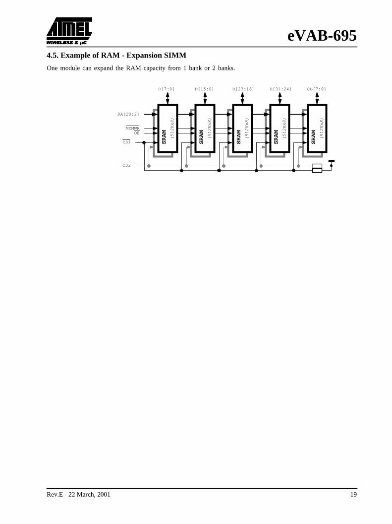
4.5. Example of RAM - Expansion SIMMOne module can expand the RAM capacity from 1 bank or 2 banks.
RA[20:2]
D[7:0] D[15:8] D[23:16] D[31:24] CB[7:0]
MEMWROE
CS1 SR
AM
(51
2K
x8)
SR
AM
(51
2K
x8)
SR
AM
(51
2K
x8)
SR
AM
(51
2K
x8)
SR
AM
(51
2K
x8)
CS2
Rev.E - 22 March, 2001 19
eVAB-695
ered in
5. FPGA
The eVAB-695 can run without the FPGA. The FPGA is useful to add some functions to the board.
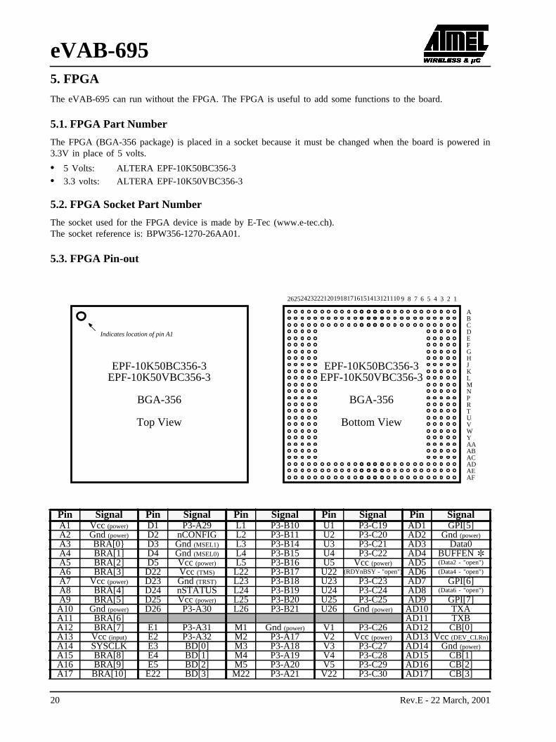
5.1. FPGA Part Number
The FPGA (BGA-356 package) is placed in a socket because it must be changed when the board is pow3.3V in place of 5 volts.
• 5 Volts: ALTERA EPF-10K50BC356-3
• 3.3 volts: ALTERA EPF-10K50VBC356-3
5.2. FPGA Socket Part Number
The socket used for the FPGA device is made by E-Tec (www.e-tec.ch).The socket reference is: BPW356-1270-26AA01.
5.3. FPGA Pin-out
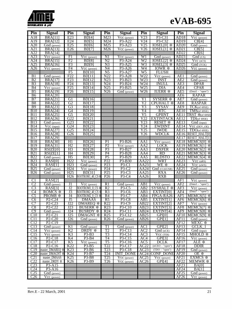
Pin Signal Pin Signal Pin Signal Pin Signal Pin SignalA1 Vcc (power) D1 P3-A29 L1 P3-B10 U1 P3-C19 AD1 GPI[5]A2 Gnd(power) D2 nCONFIG L2 P3-B11 U2 P3-C20 AD2 Gnd(power)
A3 BRA[0 D3 Gnd (MSEL1) L3 P3-B14 U3 P3-C21 AD3 Data0A4 BRA[1] D4 Gnd(MSEL0) L4 P3-B15 U4 P3-C22 AD4 BUFFENA5 BRA[2] D5 Vcc (power) L5 P3-B16 U5 Vcc(power) AD5 (Data2 - "open")
A6 BRA[3] D22 Vcc (TMS) L22 P3-B17 U22 (RDYnBSY - "open") AD6 (Data4 - "open")
A7 Vcc (power) D23 Gnd(TRST) L23 P3-B18 U23 P3-C23 AD7 GPI[6]A8 BRA[4] D24 nSTATUS L24 P3-B19 U24 P3-C24 AD8 (Data6 - "open")
A9 BRA[5] D25 Vcc (power) L25 P3-B20 U25 P3-C25 AD9 GPI[7]A10 Gnd(power) D26 P3-A30 L26 P3-B21 U26 Gnd(power) AD10 TXAA11 BRA[6] AD11 TXBA12 BRA[7] E1 P3-A31 M1 Gnd(power) V1 P3-C26 AD12 CB[0]A13 Vcc (input) E2 P3-A32 M2 P3-A17 V2 Vcc(power) AD13 Vcc (DEV_CLRn)
A14 SYSCLK E3 BD[0] M3 P3-A18 V3 P3-C27 AD14 Gnd(power)
A15 BRA[8] E4 BD[1] M4 P3-A19 V4 P3-C28 AD15 CB[1]A16 BRA[9] E5 BD[2] M5 P3-A20 V5 P3-C29 AD16 CB[2]A17 BRA[10] E22 BD[3] M22 P3-A21 V22 P3-C30 AD17 CB[3]
1234567891011121314151617181920212223242526
ABCDEFGHJKLMNPRTUVWYAAABACADAEAF
EPF-10K50BC356-3EPF-10K50VBC356-3
BGA-356
Bottom View
EPF-10K50BC356-3EPF-10K50VBC356-3
BGA-356
Top View
Indicates location of pin A1
20 Rev.E - 22 March, 2001
eVAB-695
A18 BRA[11] E23 BD[4] M23 Vcc(power) V23 P3-C31 AD18 Vcc(power)
A19 BRA[12] E24 BD[5] M24 P3-A22 V24 P3-C32 AD19 CB[4]A20 Gnd(power) E25 BD[6] M25 P3-A23 V25 IOSEL[0] AD20 Gnd(power)
A21 BRA[13] E26 BD[7] M26 Vcc(power) V26 IOSEL[1] AD21 CB[5]A22 BRA[14] AD22 CB[6]A23 Vcc (power) F1 Vcc(power) N1 Vcc (power) W1 Gnd(power) AD23 Gnd(CS)
A24 BRA[15] F2 BD[8] N2 P3-A24 W2 IOSEL[2] AD24 Vcc (nCS)
A25 BRA[16] F3 BD[9] N3 P3-A25 W3 IOSEL[3] AD25 Gnd(TCK)
A26 Vcc (power) F4 Vcc(power) N4 P3-A26 W4 IOWR AD26 Vcc (power)
F5 BD[10] N5 P3-A27 W5 FLUSHB1 Gnd(power) F22 BD[11] N22 P3-A28 W22 Vcc(power) AE1 Gnd(power)
B2 BRA[17] F23 BD[12] N23 P3-B23 W23 INST AE2 Gnd(power)
B3 BRA[18] F24 BD[13] N24 P3-B24 W24 INULL AE3 DPARB4 Vcc (power) F25 BD[14] N25 P3-B25 W25 DIA AE4 CPARB5 BRA[19] F26 BD[15] N26 Gnd(power) W26 IUERR AE5 (Data5 - "open")
B6 BRA[20] AE6 RAPARB7 BRA[21] G1 BD[16] Y1 SYSERR AE7 Gnd(power)
B8 BRA[22] G2 BD[17] Y2 CPUHALT AE8 RASPARB9 BRA[23] G3 BD[18] Y3 SYSAV AE9 TCK(of 695E)
B10 BRA[24] G4 BD[19] Y4 RTC AE10 TMS(of 695E)
B11 BRA[25] G5 BD[20] Y5 GPIINT AE11 TRST(of 695E)
B12 BRA[26] G22 BD[21] Y22 EXTINTACK AE12 TDI(of 695E)
B13 Gnd(power) G23 BD[22] Y23 RESET AE13 Gnd(input)
B14 Vcc(input) G24 BD[23] Y24 EWDINT AE14 Vcc(DEV_OE)
B15 BRA[27] G25 BD[24] Y25 IWDE AE15 TDO(of 695E)
B16 BRA[28] G26 BD[25] Y26 WDCLK AE16 RESET_HALT[0]B17 BRA[29] AE17 RESET_HALT[1]B18 BRA[30] H1 BD[26] P1 P3-B26 AA1 Vcc(power) AE18 MEMCS[0] B19 BRA[31] H2 BD[27] P2 Vcc(power) AA2 LOCK AE19 MEMCS[1] B20 RSIZE[0] H3 BD[28] P3 P3-B27 AA3 DXFER AE20 MEMCS[2]B21 RSIZE[1] H4 BD[29] P4 P3-B28 AA4 RD AE21 MEMCS[3]B22 Gnd(power) H5 BD[30] P5 P3-B29 AA5 RLDSTO AE22 MEMCS[4]B23 RASI[0] H22 Vcc(power) P22 P3-B30 AA22 WRT AE23 Vcc(nRS)
B24 RASI[1] H23 Gnd(power) P23 P3-C1 AA23 WE AE24 Vcc(nWS)
B25 Gnd(power) H24 Vcc(power) P24 P3-C2 AA24 Gnd(CLKUSR) AE25 Gnd(power)
B26 Gnd(power) H25 BD[31] P25 P3-C3 AA25 RXA AE26 Gnd(power)
H26 BOOTROM1_40_CS P26 P3-C4 AA26 RXBC1 RASI[2] AF1 Vcc (power)
C2 Gnd(power) J1 Vcc(power) R1 Gnd(power) AB1 Vcc (power) AF2 (Data3 - "open")
C3 RASI[3] J2 BOOTROM1_8_CS R2 P3-C5 AB2 SYSHALT AF3 Vcc (power)
C4 ROMCS J3 BOOTROM2_40_CS R3 P3-C6 AB3 EXTINT[0] AF4 (Data7 - "open")
C5 PROM8 J4 BOOTROM2_8_CS R4 P3-C7 AB4 FPGA-RA26 AF5 MEMCS[5]C6 P2-C24 J5 DMAAS R5 P3-C8 AB5 EXTINT[1] AF6 MEMCS[6]C7 P2-C23 J22 DMAREQ R22 P3-C9 AB22 EXTINT[2] AF7 Vcc(power)
C8 P2-C22 J23 BUSERR R23 P3-C10 AB23 EXTINT[3] AF8 MEMCS[7]C9 Gnd(power) J24 BUSRDY R24 P3-C11 AB24 EXTINT[4] AF9 MEMCS[8]C10 P2-C21 J25 DMAGNT R25 P3-C12 AB25 GPI[0] AF10 MEMCS[9]C11 P2-C20 J26 Gnd(power) R26 Gnd(power) AB26 GPI[1] AF11 Gnd(power)
C12 P2-C19 AF12 MEXC C13 Gnd(power) K1 Gnd(power) T1 Gnd(power) AC1 GPI[2] AF13 GCLK_1C14 Vcc(power) K2 DRDY T2 P3-C13 AC2 Gnd(nCE) AF14 Gnd(input)
C15 Vcc(power) K3 P3-B3 T3 P3-C14 AC3 Vcc(TDI) AF15 MHOLD C16 P2-C18 K4 P3-B4 T4 P3-C15 AC4 GPI[3] AF16 Vcc(power)
C17 P2-C17 K5 Vcc(power) T5 P3-C16 AC5 DCLK AF17 ALEC18 P2-C16 K22 P3-B5 T22 P3-C17 AC22(nCEO - "open") AF18 DDIRC19 master_DMAREQ K23 P3-B6 T23 P3-C18 AC23 (TDO - "open") AF19 Gnd(power)
C20 master_DMAGNT K24 P3-B7 T24 INIT_DONE AC24 CONF_DONE AF20 OEC21 master_DMAAS K25 P3-B8 T25 Vcc(power) AC25 Vcc(power) AF21 EXMCS C22 master_DRDY K26 P3-B9 T26 Vcc(power) AC26 GPI[4] AF22 MEMWRC23 P3-A15 AF23 BA[0]C24 P3-A16 AF24 BA[1]C25 Gnd(power) AF25 Gnd(power)
C26 Vcc(power) AF26 Vcc(power)
Pin Signal Pin Signal Pin Signal Pin Signal Pin Signal
Rev.E - 22 March, 2001 21
eVAB-695
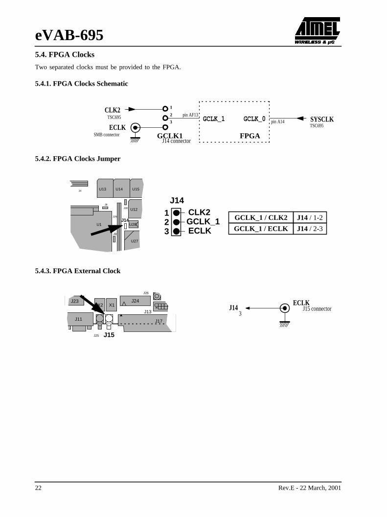
5.4. FPGA ClocksTwo separated clocks must be provided to the FPGA.
5.4.1. FPGA Clocks Schematic
5.4.2. FPGA Clocks Jumper
5.4.3. FPGA External Clock
FPGAECLK
SMB connector
CLK2SYSCLKTSC695
TSC695 GCLK_0GCLK_1
GCLK1
1
2
3
pin AF13pin A14
J14 connector
J14
GCLK_1CLK2
ECLK
123 J14 / 2-3
J14 / 1-2
GCLK_1 / ECLK
GCLK_1 / CLK2U12
U1
U27
U28
J8
J9
J29
J30
J14
U15U14U13J4
J26
J24J23
J11 J17
J13
J25 J15
J143
X1X2 ECLKJ15 connector
22 Rev.E - 22 March, 2001
eVAB-695
8-pin
rterrs on
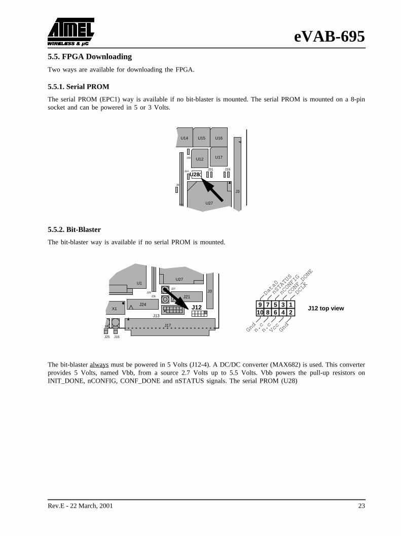
5.5. FPGA Downloading
Two ways are available for downloading the FPGA.
5.5.1. Serial PROM
The serial PROM (EPC1) way is available if no bit-blaster is mounted. The serial PROM is mounted on asocket and can be powered in 5 or 3 Volts.
5.5.2. Bit-Blaster
The bit-blaster way is available if no serial PROM is mounted.
The bit-blasteralways must be powered in 5 Volts (J12-4). A DC/DC converter (MAX682) is used. This conveprovides 5 Volts, named Vbb, from a source 2.7 Volts up to 5.5 Volts. Vbb powers the pull-up resistoINIT_DONE, nCONFIG, CONF_DONE and nSTATUS signals. The serial PROM (U28)
U12
J3
U27
J9
J30
J14J16
U17
U16U15U14
J29
J31
U28
J26
J3J21
J24
J17
U1U27
J12J13
J25 J15
J27
X1
J29
135246
79810
J12 top view
Gnd
n.c
n.c
Vcc Gnd
Data0
nSTATUS
nCONFIG
CONF_D
ONE
DCLK
Rev.E - 22 March, 2001 23
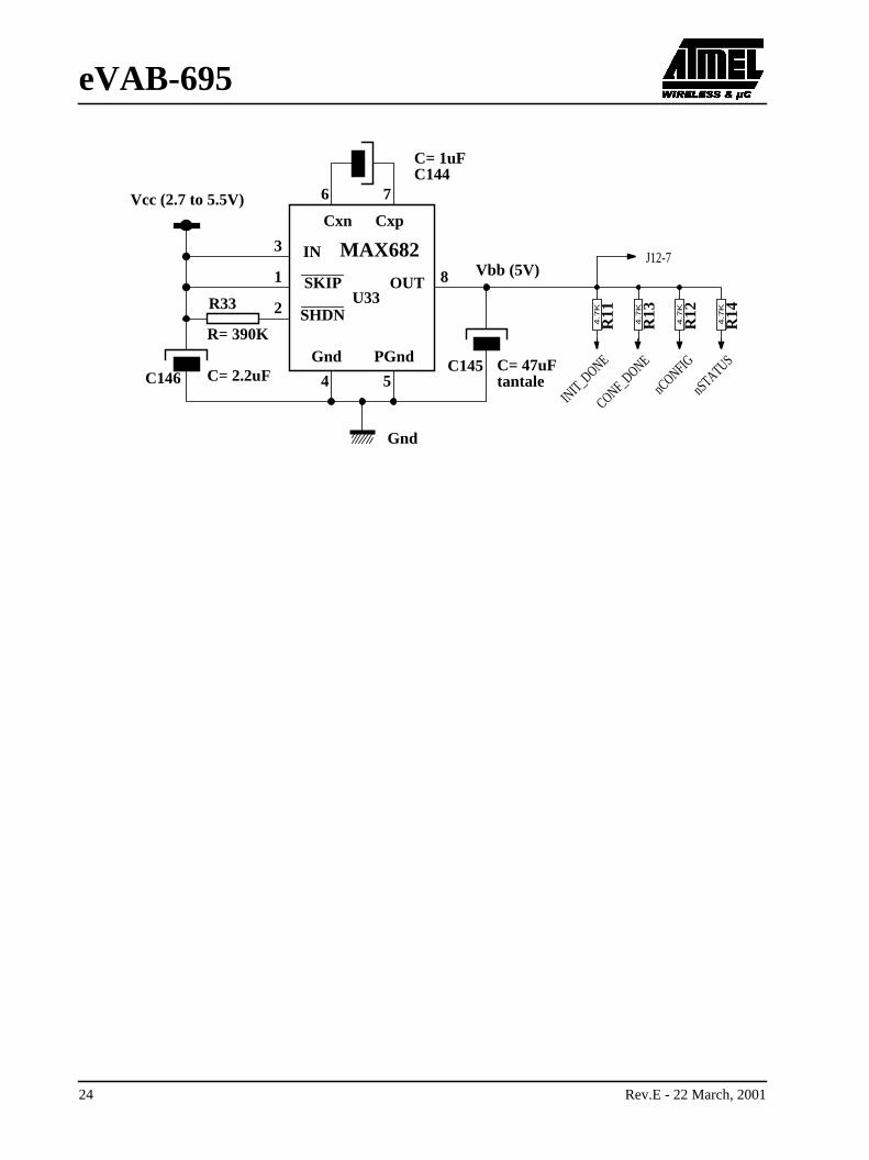
eVAB-695
IN
SKIP
SHDN
Gnd PGnd
OUT
Cxn CxpVcc (2.7 to 5.5V)
R= 390K
3
1
2
C= 1uF
C= 2.2uF
Vbb (5V)
C= 47uF
6 7
8
4 5
Gnd
J12-7
tantale
4.7
K
4.7
K
4.7
K
4.7
K
INIT_DONE
CONF_DONE
nCONFIG
nSTATUS
R11
R12
R13
R14
C144
C145
U33R33
C146
MAX682
24 Rev.E - 22 March, 2001
eVAB-695
target,ddressterthe boot-
space
6. DMA
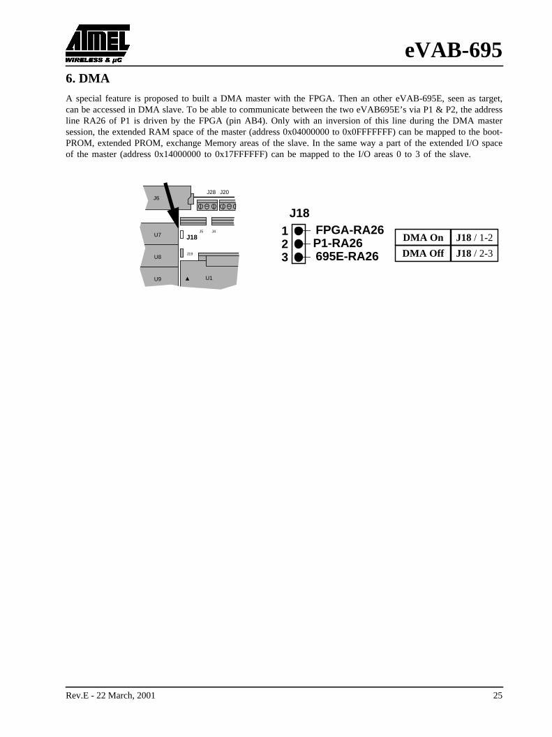
A special feature is proposed to built a DMA master with the FPGA. Then an other eVAB-695E, seen ascan be accessed in DMA slave. To be able to communicate between the two eVAB695E’s via P1 & P2, the aline RA26 of P1 is driven by the FPGA (pin AB4). Only with an inversion of this line during the DMA massession, the extended RAM space of the master (address 0x04000000 to 0x0FFFFFFF) can be mapped toPROM, extended PROM, exchange Memory areas of the slave. In the same way a part of the extended I/Oof the master (address 0x14000000 to 0x17FFFFFF) can be mapped to the I/O areas 0 to 3 of the slave.
J6
U1
U7
U8
U9
J28
J5 J4
J18
J19
J18
P1-RA26FPGA-RA26
695E-RA26
123 J18 / 2-3
J18 / 1-2
DMA Off
DMA On
J20
Rev.E - 22 March, 2001 25
eVAB-695
20 and
or.
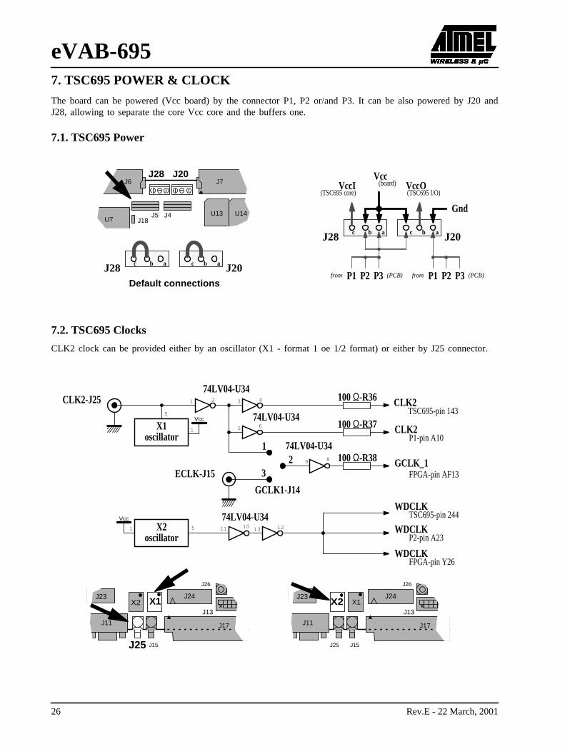
7. TSC695 POWER & CLOCK
The board can be powered (Vcc board) by the connector P1, P2 or/and P3. It can be also powered by JJ28, allowing to separate the core Vcc core and the buffers one.
7.1. TSC695 Power
7.2. TSC695 Clocks
CLK2 clock can be provided either by an oscillator (X1 - format 1 oe 1/2 format) or either by J25 connect
Vcc(board)
J28 J20c b a c b a
from P1 P2 P3
VccO(TSC695 I/O)
VccI(TSC695 core)
Gnd
J7J6
U7U14U13J5 J4
J18
J28 J20
J28 J20c b a c b a
(PCB) from P1 P2 P3 (PCB)Default connections
CLK2-J25
X1oscillator
CLK2TSC695-pin 143
CLK2P1-pin A10
GCLK_1FPGA-pin AF13
12
3
GCLK1-J14
ECLK-J15
74LV04-U34
X2oscillator
WDCLKTSC695-pin 244
WDCLKP2-pin A23
WDCLKFPGA-pin Y26
74LV04-U34
74LV04-U34
100Ω-R36
100Ω-R37
100Ω-R38
J26
J24J23
J11 J17
J13
J25 J15
X1X2
J26
J24J23
J11 J17
J13
J25 J15
X1X2
Vcc
Vcc
1
1 5
5
1 2 3 4
5 6
9 8
11 10 13 12
74LV04-U34
26 Rev.E - 22 March, 2001
eVAB-695
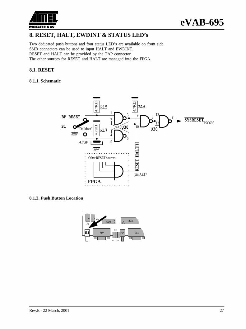
8. RESET, HALT, EWDINT & STATUS LED’sTwo dedicated push buttons and four status LED’s are available on front side.SMB connectors can be used to input HALT and EWDINT.RESET and HALT can be provided by the TAP connector.The other sources for RESET and HALT are managed into the FPGA.
8.1. RESET
8.1.1. Schematic
8.1.2. Push Button Location
4.7K
Ω
BP RESET
"On-Mom"
Other RESET sources
FPGA
SYSRESET
4.7K
Ω
TSC695
4.7µF
4.7K
Ω
pin AE17
65
4
32
1
U30R17
R15
89
10
1112
13
U30
R16
S1
RESE
T_HA
LT[1
]
J2
J1J23
J10 J11S2S1
D3D1
D2
U29
Rev.E - 22 March, 2001 27
eVAB-695
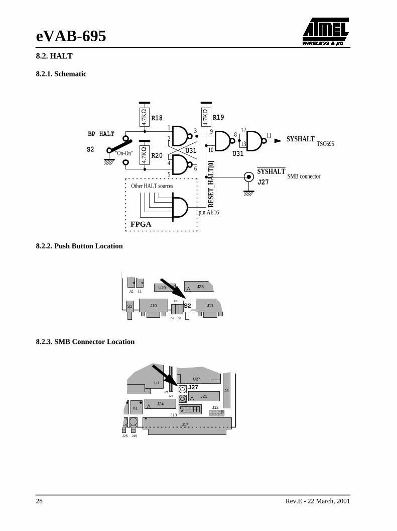
8.2. HALT8.2.1. Schematic
8.2.2. Push Button Location
8.2.3. SMB Connector Location
4.7K
Ω
BP HALT
"On-On"
Other HALT sources
FPGA
SYSHALT4.
7KΩ
TSC695
4.7K
Ω
SYSHALTSMB connector
pin AE16
65
4
32
1
U31R20
R18
89
10
1112
13
U31
J27
S2
R19
RESE
T_HA
LT[0
]
J2 J1J23
J10 J11S2S1
D3D1
D2
U29
J26
J3J21
J24
J17
U1U27
J12
J13
J25 J15
J27
X1
J29
28 Rev.E - 22 March, 2001
eVAB-695
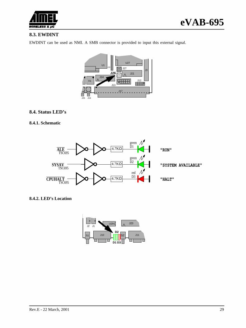
8.3. EWDINTEWDINT can be used as NMI. A SMB connector is provided to input this external signal.
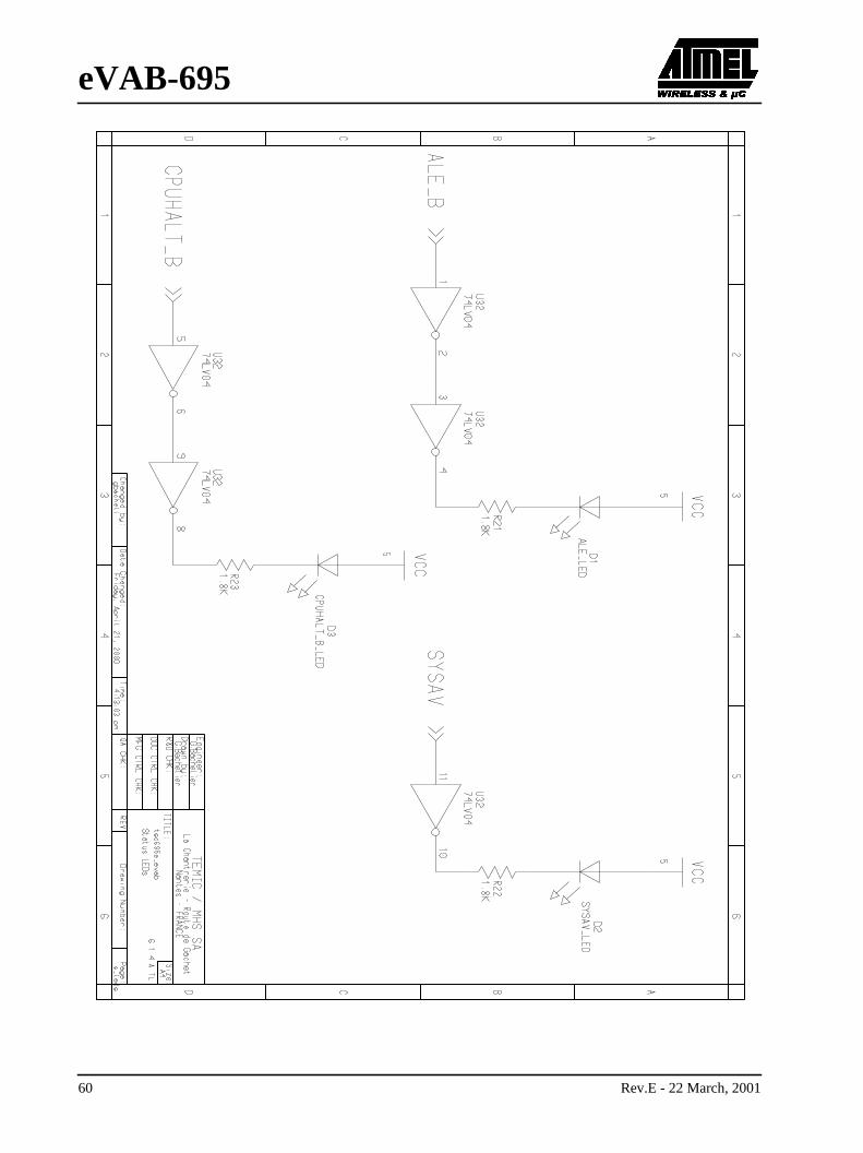
8.4. Status LED’s
8.4.1. Schematic
8.4.2. LED’s Location
J26J3
J21J24
J17
U1U27
J12
J13
J25 J15
J27J29
X1
CPUHALT "HALT"4.7KΩred
"SYSTEM AVAILABLE"4.7KΩgreen
TSC695
"RUN"4.7KΩgreen
SYSAVTSC695
ALETSC695
D1
D2
D3
J2 J1J23
J10 J11S2S1
D3D1
D2
U29
Rev.E - 22 March, 2001 29
eVAB-695
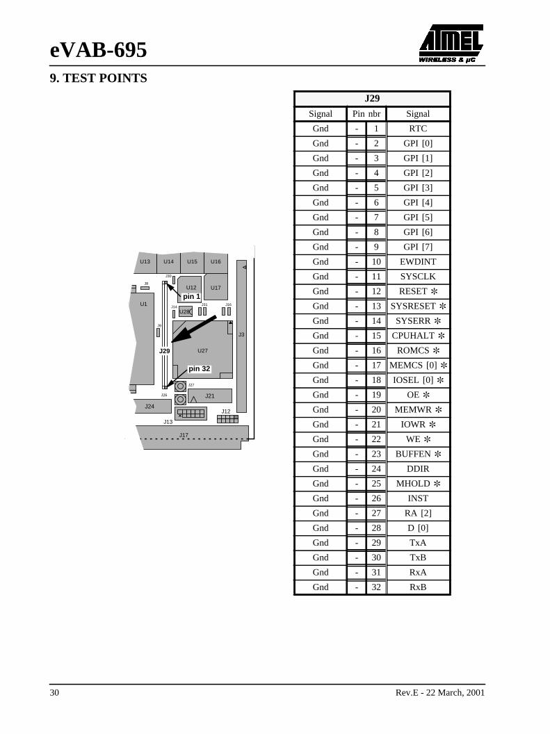
9. TEST POINTSJ29
Signal Pin nbr Signal
Gnd - 1 RTC
Gnd - 2 GPI [0]
Gnd - 3 GPI [1]
Gnd - 4 GPI [2]
Gnd - 5 GPI [3]
Gnd - 6 GPI [4]
Gnd - 7 GPI [5]
Gnd - 8 GPI [6]
Gnd - 9 GPI [7]
Gnd - 10 EWDINT
Gnd - 11 SYSCLK
Gnd - 12 RESET
Gnd - 13 SYSRESET
Gnd - 14 SYSERR
Gnd - 15 CPUHALT
Gnd - 16 ROMCS
Gnd - 17 MEMCS [0]
Gnd - 18 IOSEL [0]
Gnd - 19 OE
Gnd - 20 MEMWR
Gnd - 21 IOWR
Gnd - 22 WE
Gnd - 23 BUFFEN
Gnd - 24 DDIR
Gnd - 25 MHOLD
Gnd - 26 INST
Gnd - 27 RA [2]
Gnd - 28 D [0]
Gnd - 29 TxA
Gnd - 30 TxB
Gnd - 31 RxA
Gnd - 32 RxB
J26
U12
J3
J21
J24
J17
U1
U27
U28
J12
J13
J27
J8
J9
J30
J14J16
U17
U16U15U14U13
J29
pin 1
pin 32
J31
30 Rev.E - 22 March, 2001
eVAB-695
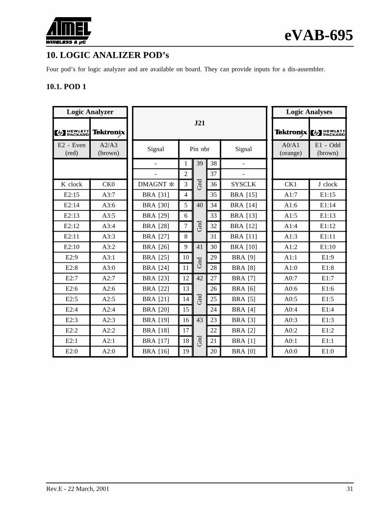
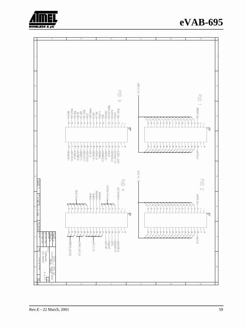
10. LOGIC ANALIZER POD’sFour pod’s for logic analyzer and are available on board. They can provide inputs for a dis-assembler.
10.1. POD 1
Logic Analyzer
J21
Logic Analyses
E2 - Even(red)
A2/A3(brown)
Signal Pin nbr SignalA0/A1
(orange)E1 - Odd(brown)
- 1 39 38 -
- 2
Gnd
37 -
K clock CK0 DMAGNT 3 36 SYSCLK CK1 J clock
E2:15 A3:7 BRA [31] 4 35 BRA [15] A1:7 E1:15
E2:14 A3:6 BRA [30] 5 40 34 BRA [14] A1:6 E1:14
E2:13 A3:5 BRA [29] 6
Gnd
33 BRA [13] A1:5 E1:13
E2:12 A3:4 BRA [28] 7 32 BRA [12] A1:4 E1:12
E2:11 A3:3 BRA [27] 8 31 BRA [11] A1:3 E1:11
E2:10 A3:2 BRA [26] 9 41 30 BRA [10] A1:2 E1:10
E2:9 A3:1 BRA [25] 10
Gnd
29 BRA [9] A1:1 E1:9
E2:8 A3:0 BRA [24] 11 28 BRA [8] A1:0 E1:8
E2:7 A2:7 BRA [23] 12 42 27 BRA [7] A0:7 E1:7
E2:6 A2:6 BRA [22] 13
Gnd
26 BRA [6] A0:6 E1:6
E2:5 A2:5 BRA [21] 14 25 BRA [5] A0:5 E1:5
E2:4 A2:4 BRA [20] 15 24 BRA [4] A0:4 E1:4
E2:3 A2:3 BRA [19] 16 43 23 BRA [3] A0:3 E1:3
E2:2 A2:2 BRA [18] 17
Gnd
22 BRA [2] A0:2 E1:2
E2:1 A2:1 BRA [17] 18 21 BRA [1] A0:1 E1:1
E2:0 A2:0 BRA [16] 19 20 BRA [0] A0:0 E1:0
Rev.E - 22 March, 2001 31
eVAB-695
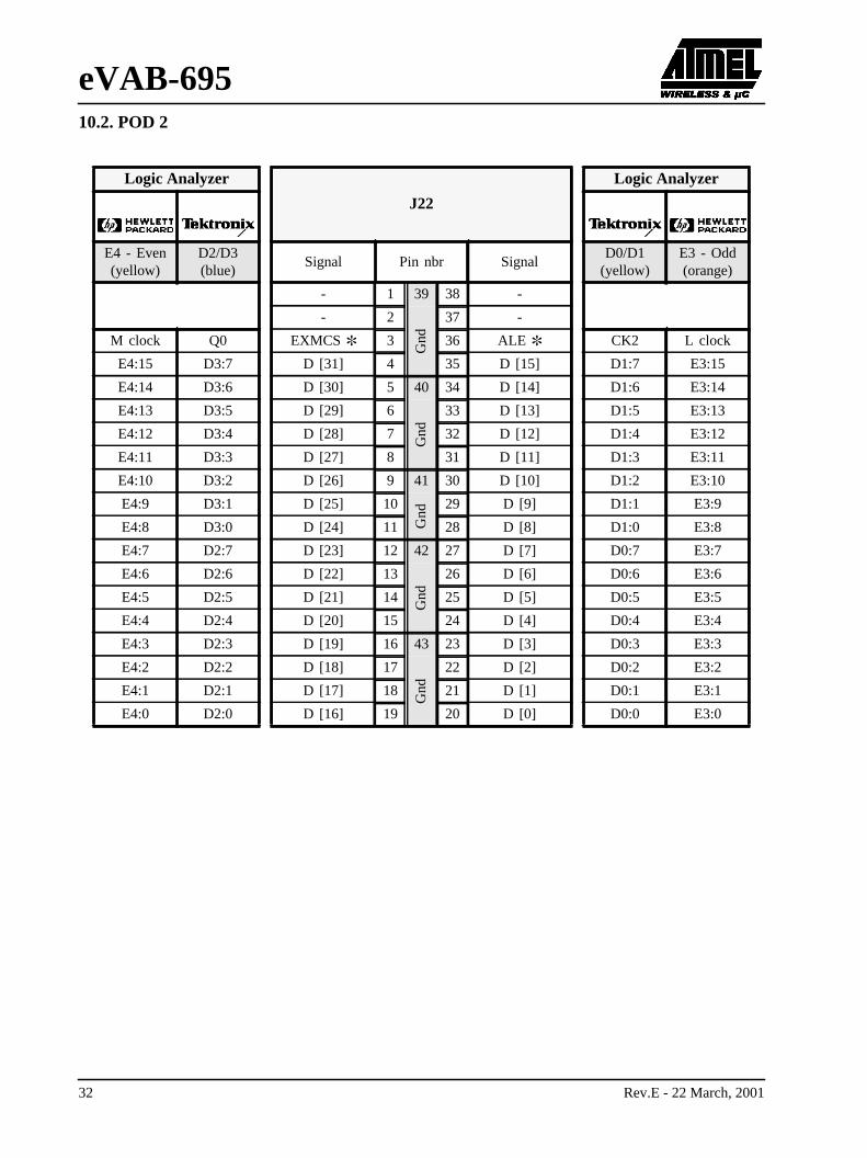
10.2. POD 2Logic Analyzer
J22
Logic Analyzer
E4 - Even(yellow)
D2/D3(blue)
Signal Pin nbr SignalD0/D1
(yellow)E3 - Odd(orange)
- 1 39 38 -
- 2
Gnd
37 -
M clock Q0 EXMCS 3 36 ALE CK2 L clock
E4:15 D3:7 D [31] 4 35 D [15] D1:7 E3:15
E4:14 D3:6 D [30] 5 40 34 D [14] D1:6 E3:14
E4:13 D3:5 D [29] 6G
nd33 D [13] D1:5 E3:13
E4:12 D3:4 D [28] 7 32 D [12] D1:4 E3:12
E4:11 D3:3 D [27] 8 31 D [11] D1:3 E3:11
E4:10 D3:2 D [26] 9 41 30 D [10] D1:2 E3:10
E4:9 D3:1 D [25] 10
Gnd
29 D [9] D1:1 E3:9
E4:8 D3:0 D [24] 11 28 D [8] D1:0 E3:8
E4:7 D2:7 D [23] 12 42 27 D [7] D0:7 E3:7
E4:6 D2:6 D [22] 13
Gnd
26 D [6] D0:6 E3:6
E4:5 D2:5 D [21] 14 25 D [5] D0:5 E3:5
E4:4 D2:4 D [20] 15 24 D [4] D0:4 E3:4
E4:3 D2:3 D [19] 16 43 23 D [3] D0:3 E3:3
E4:2 D2:2 D [18] 17
Gnd
22 D [2] D0:2 E3:2
E4:1 D2:1 D [17] 18 21 D [1] D0:1 E3:1
E4:0 D2:0 D [16] 19 20 D [0] D0:0 E3:0
32 Rev.E - 22 March, 2001
eVAB-695
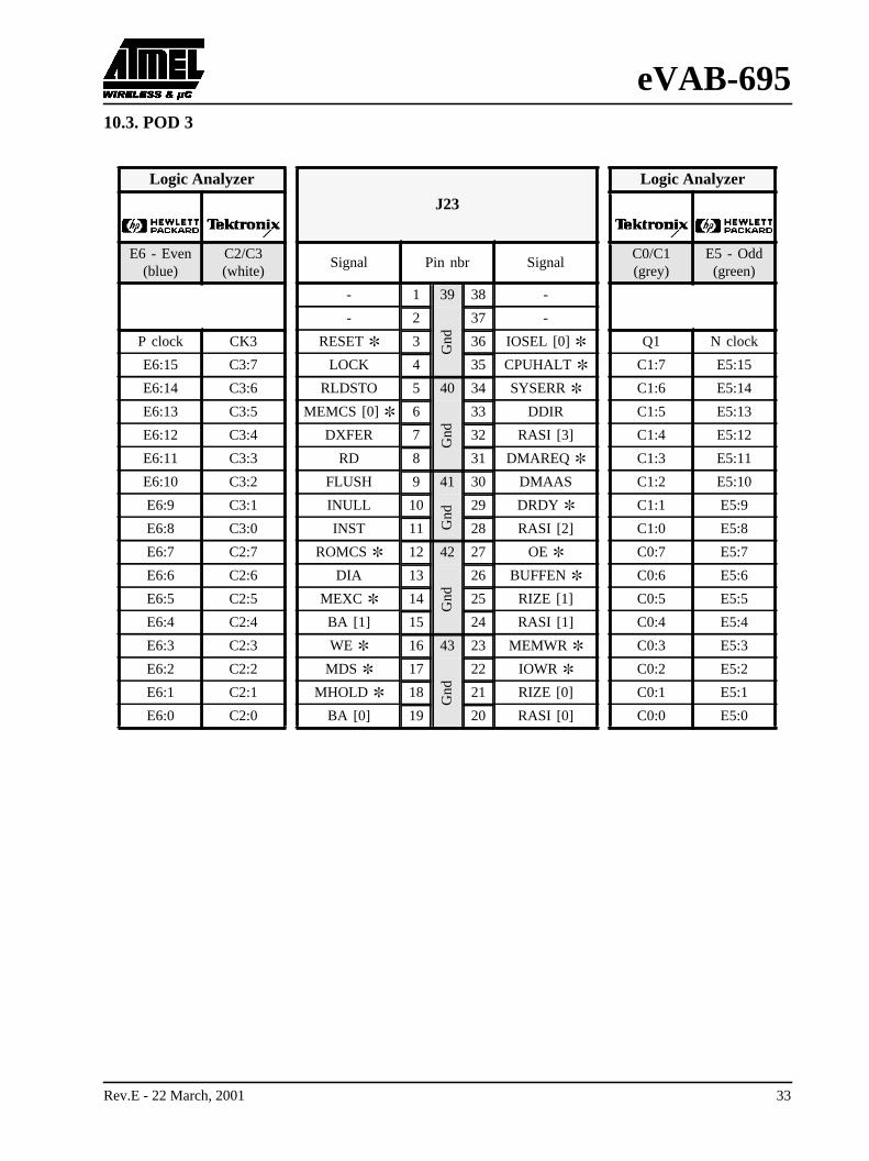
10.3. POD 3Logic Analyzer
J23
Logic Analyzer
E6 - Even(blue)
C2/C3(white)
Signal Pin nbr SignalC0/C1(grey)
E5 - Odd(green)
- 1 39 38 -
- 2
Gnd
37 -
P clock CK3 RESET 3 36 IOSEL [0] Q1 N clock
E6:15 C3:7 LOCK 4 35 CPUHALT C1:7 E5:15
E6:14 C3:6 RLDSTO 5 40 34 SYSERR C1:6 E5:14
E6:13 C3:5 MEMCS [0] 6
Gnd
33 DDIR C1:5 E5:13
E6:12 C3:4 DXFER 7 32 RASI [3] C1:4 E5:12
E6:11 C3:3 RD 8 31 DMAREQ C1:3 E5:11
E6:10 C3:2 FLUSH 9 41 30 DMAAS C1:2 E5:10
E6:9 C3:1 INULL 10
Gnd
29 DRDY C1:1 E5:9
E6:8 C3:0 INST 11 28 RASI [2] C1:0 E5:8
E6:7 C2:7 ROMCS 12 42 27 OE C0:7 E5:7
E6:6 C2:6 DIA 13
Gnd
26 BUFFEN C0:6 E5:6
E6:5 C2:5 MEXC 14 25 RIZE [1] C0:5 E5:5
E6:4 C2:4 BA [1] 15 24 RASI [1] C0:4 E5:4
E6:3 C2:3 WE 16 43 23 MEMWR C0:3 E5:3
E6:2 C2:2 MDS 17
Gnd
22 IOWR C0:2 E5:2
E6:1 C2:1 MHOLD 18 21 RIZE [0] C0:1 E5:1
E6:0 C2:0 BA [0] 19 20 RASI [0] C0:0 E5:0
Rev.E - 22 March, 2001 33
eVAB-695
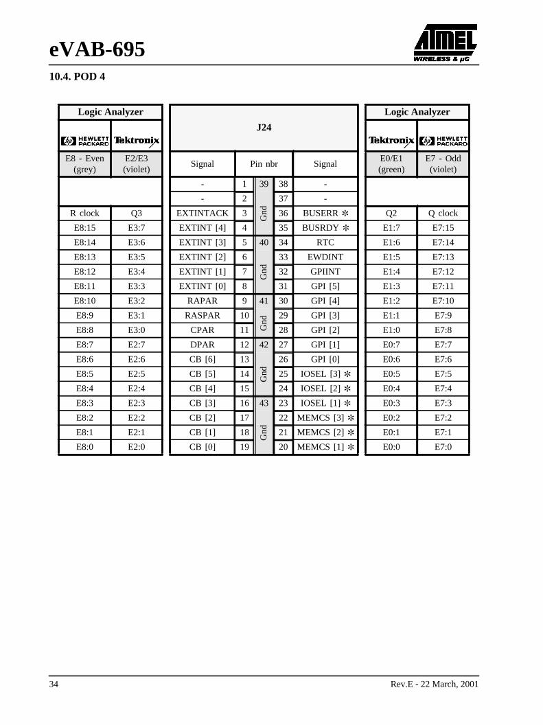
10.4. POD 4Logic Analyzer
J24
Logic Analyzer
E8 - Even(grey)
E2/E3(violet)
Signal Pin nbr SignalE0/E1(green)
E7 - Odd(violet)
- 1 39 38 -
- 2
Gnd
37 -
R clock Q3 EXTINTACK 3 36 BUSERR Q2 Q clock
E8:15 E3:7 EXTINT [4] 4 35 BUSRDY E1:7 E7:15
E8:14 E3:6 EXTINT [3] 5 40 34 RTC E1:6 E7:14
E8:13 E3:5 EXTINT [2] 6G
nd33 EWDINT E1:5 E7:13
E8:12 E3:4 EXTINT [1] 7 32 GPIINT E1:4 E7:12
E8:11 E3:3 EXTINT [0] 8 31 GPI [5] E1:3 E7:11
E8:10 E3:2 RAPAR 9 41 30 GPI [4] E1:2 E7:10
E8:9 E3:1 RASPAR 10
Gnd
29 GPI [3] E1:1 E7:9
E8:8 E3:0 CPAR 11 28 GPI [2] E1:0 E7:8
E8:7 E2:7 DPAR 12 42 27 GPI [1] E0:7 E7:7
E8:6 E2:6 CB [6] 13
Gnd
26 GPI [0] E0:6 E7:6
E8:5 E2:5 CB [5] 14 25 IOSEL [3] E0:5 E7:5
E8:4 E2:4 CB [4] 15 24 IOSEL [2] E0:4 E7:4
E8:3 E2:3 CB [3] 16 43 23 IOSEL [1] E0:3 E7:3
E8:2 E2:2 CB [2] 17
Gnd
22 MEMCS [3] E0:2 E7:2
E8:1 E2:1 CB [1] 18 21 MEMCS [2] E0:1 E7:1
E8:0 E2:0 CB [0] 19 20 MEMCS [1] E0:0 E7:0
34 Rev.E - 22 March, 2001
eVAB-695
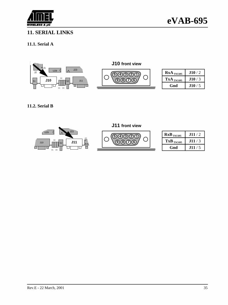
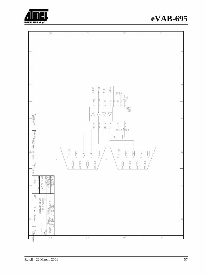
11. SERIAL LINKS11.1. Serial A
11.2. Serial B
1
J10 front view
J10 / 5
J10 / 3
Gnd
TxA TSC695
J2
J1J23
J10 J11S1
U29
D3D1
D2
S2
J10 / 2RxA TSC695569
23478
J23
J10
D3D1
D2
U29
J11J25
S2
1
J11 front view
J11 / 5
J11 / 3
Gnd
TxB TSC695
J11 / 2RxB TSC695569
23478
Rev.E - 22 March, 2001 35
eVAB-695
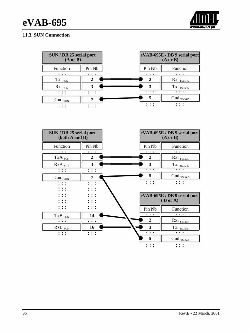
11.3. SUN Connection. . . . . .
. . . . . .. . . . . .
. . . . . .. . . . . . . . .. . . . . .. . .
. . . . . . . . .. . .
. . . . . . . . .. . .. . . . . .5 GndTSC695
eVAB-695E / DB 9 serial port
Pin Nb
(A or B)
Function
SUN / DB 25 serial port
Pin Nb
(both A and B)
Function
2TxA SUN 2 Rx. TSC695
3RxA SUN 3 Tx. TSC695
. . . . . .. . . . . . . . .. . . . . .. . .
. . . . . . . . .. . .
. . . . . . . . .. . .. . . . . .5 GndTSC695
eVAB-695E / DB 9 serial port
Pin Nb
(A or B)
Function
SUN / DB 25 serial port
Pin Nb
(A or B)
Function
2Tx. SUN 2 Rx. TSC695
3Rx. SUN 3 Tx. TSC695
7GndSUN
. . .. . .
. . . . . .. . . . . .
eVAB-695E / DB 9 serial port
Pin Nb
( B or A)
Function
14TxB SUN
2 Rx. TSC695
16RxB SUN 3 Tx. TSC695
. . . . . .. . . . . .
. . . . . .. . . . . .
. . . . . .. . . . . .
7GndSUN
. . .. . . . . .. . .
. . .. . .5 GndTSC695
36 Rev.E - 22 March, 2001
eVAB-695
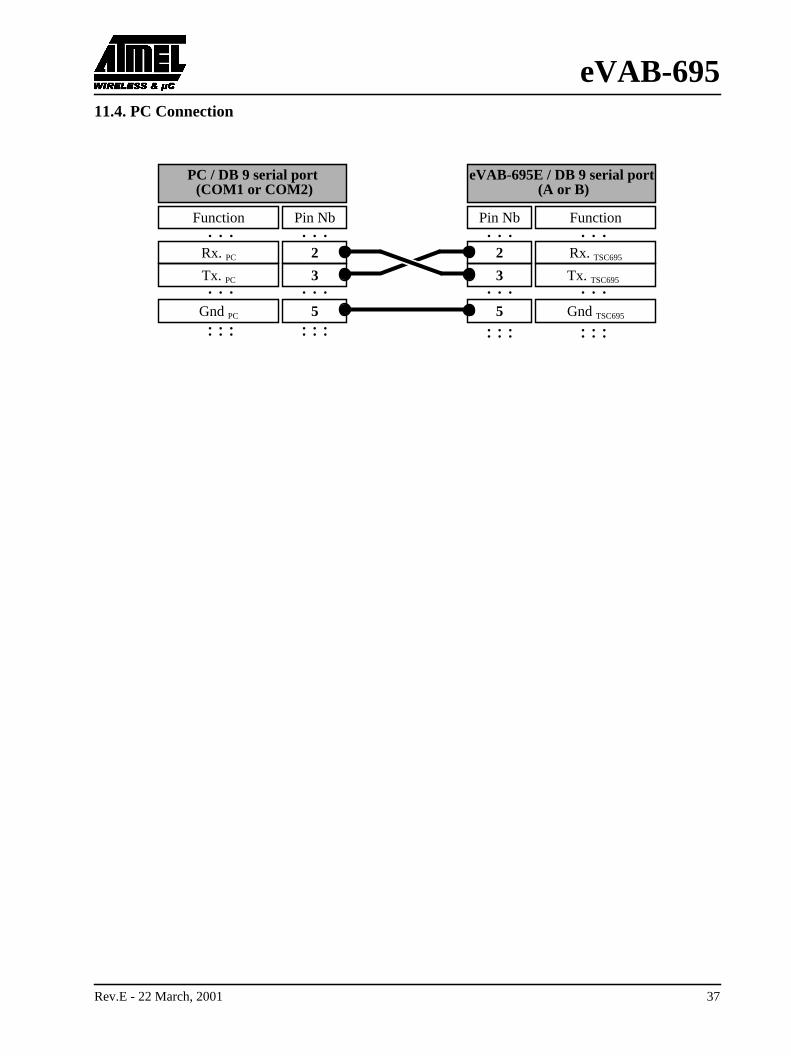
11.4. PC Connection. . . . . .. . . . . . . . .. . . . . .. . .
. . . . . . . . .. . .
. . .. . .. . . . . .5 GndTSC695
eVAB-695E / DB 9 serial port
Pin Nb
(A or B)
Function
PC / DB 9 serial port
Pin Nb
(COM1 or COM2)
Function
2Rx. PC 2 Rx. TSC695
3Tx. PC 3 Tx. TSC695
5GndPC
Rev.E - 22 March, 2001 37
eVAB-695
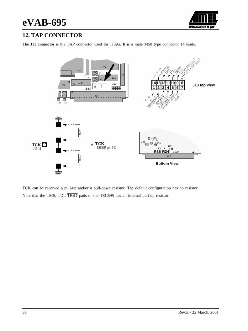
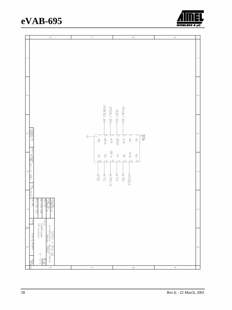
12. TAP CONNECTORThe J13 connector is the TAP connector used for JTAG. It is a male M50 type connector 14 leads.
TCK can be received a pull-up and/or a pull-down resistor. The default configuration has no resistor.
Note that the TMS, TDI,TRST pads of the TSC695 has an internal pull-up resistor.
J26
J3J21
J24
J17
U1U27
J13
J12
J25 J15
J27
X1
J29
101112543
131421
J13 top view
n.c
n.c
CPUHALT
RESETGnd
n.c
SYCLK
TMSTCK
TRST
8976
TDO(T
DI 695E)
TDI(TDO69
5E)
SYSHALT
SYSRESET
TCKJ13-11
R3
4R
35
Vcc
TCKTSC695-pin 142
J17
R7
C129
U33 C145
C146C144
R35 R34
Bottom View
38 Rev.E - 22 March, 2001
eVAB-695
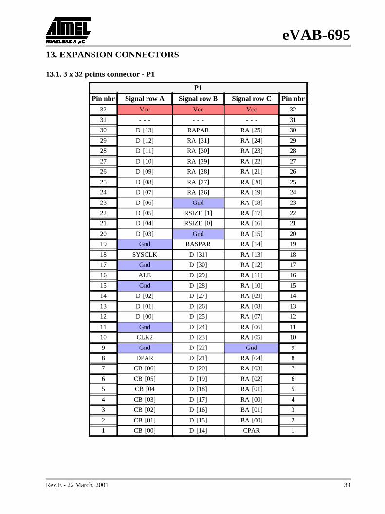
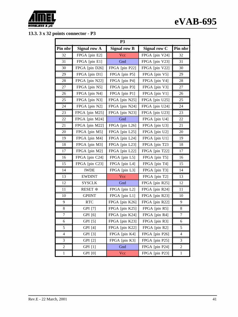
13. EXPANSION CONNECTORS13.1. 3 x 32 points connector - P1
P1
Pin nbr Signal row A Signal row B Signal row C Pin nbr
32 Vcc Vcc Vcc 32
31 - - - - - - - - - 31
30 D [13] RAPAR RA [25] 30
29 D [12] RA [31] RA [24] 29
28 D [11] RA [30] RA [23] 28
27 D [10] RA [29] RA [22] 27
26 D [09] RA [28] RA [21] 26
25 D [08] RA [27] RA [20] 25
24 D [07] RA [26] RA [19] 24
23 D [06] Gnd RA [18] 23
22 D [05] RSIZE [1] RA [17] 22
21 D [04] RSIZE [0] RA [16] 21
20 D [03] Gnd RA [15] 20
19 Gnd RASPAR RA [14] 19
18 SYSCLK D [31] RA [13] 18
17 Gnd D [30] RA [12] 17
16 ALE D [29] RA [11] 16
15 Gnd D [28] RA [10] 15
14 D [02] D [27] RA [09] 14
13 D [01] D [26] RA [08] 13
12 D [00] D [25] RA [07] 12
11 Gnd D [24] RA [06] 11
10 CLK2 D [23] RA [05] 10
9 Gnd D [22] Gnd 9
8 DPAR D [21] RA [04] 8
7 CB [06] D [20] RA [03] 7
6 CB [05] D [19] RA [02] 6
5 CB [04 D [18] RA [01] 5
4 CB [03] D [17] RA [00] 4
3 CB [02] D [16] BA [01] 3
2 CB [01] D [15] BA [00] 2
1 CB [00] D [14] CPAR 1
Rev.E - 22 March, 2001 39
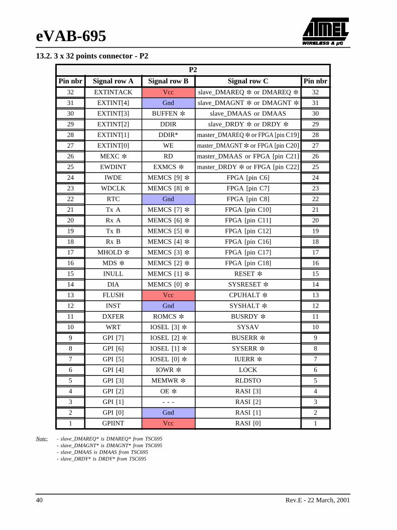
eVAB-695
13.2. 3 x 32 points connector - P2Note: - slave_DMAREQ* is DMAREQ* from TSC695- slave_DMAGNT* is DMAGNT* from TSC695- slave_DMAAS is DMAAS from TSC695- slave_DRDY* is DRDY* from TSC695
P2
Pin nbr Signal row A Signal row B Signal row C Pin nbr
32 EXTINTACK Vcc slave_DMAREQ or DMAREQ 32
31 EXTINT[4] Gnd slave_DMAGNT or DMAGNT 31
30 EXTINT[3] BUFFEN slave_DMAAS or DMAAS 30
29 EXTINT[2] DDIR slave_DRDY or DRDY 29
28 EXTINT[1] DDIR* master_DMAREQ orFPGA [pinC19] 28
27 EXTINT[0] WE master_DMAGNT or FPGA [pinC20] 27
26 MEXC RD master_DMAAS or FPGA [pin C21] 26
25 EWDINT EXMCS master_DRDY or FPGA [pin C22] 25
24 IWDE MEMCS [9] FPGA [pin C6] 24
23 WDCLK MEMCS [8] FPGA [pin C7] 23
22 RTC Gnd FPGA [pin C8] 22
21 Tx A MEMCS [7] FPGA [pin C10] 21
20 Rx A MEMCS [6] FPGA [pin C11] 20
19 Tx B MEMCS [5] FPGA [pin C12] 19
18 Rx B MEMCS [4] FPGA [pin C16] 18
17 MHOLD MEMCS [3] FPGA [pin C17] 17
16 MDS MEMCS [2] FPGA [pin C18] 16
15 INULL MEMCS [1] RESET 15
14 DIA MEMCS [0] SYSRESET 14
13 FLUSH Vcc CPUHALT 13
12 INST Gnd SYSHALT 12
11 DXFER ROMCS BUSRDY 11
10 WRT IOSEL [3] SYSAV 10
9 GPI [7] IOSEL [2] BUSERR 9
8 GPI [6] IOSEL [1] SYSERR 8
7 GPI [5] IOSEL [0] IUERR 7
6 GPI [4] IOWR LOCK 6
5 GPI [3] MEMWR RLDSTO 5
4 GPI [2] OE RASI [3] 4
3 GPI [1] - - - RASI [2] 3
2 GPI [0] Gnd RASI [1] 2
1 GPIINT Vcc RASI [0] 1
40 Rev.E - 22 March, 2001
eVAB-695
13.3. 3 x 32 points connector - P3P3
Pin nbr Signal row A Signal row B Signal row C Pin nbr
32 FPGA [pin E2] Vcc FPGA [pin V24] 32
31 FPGA [pin E1] Gnd FPGA [pin V23] 31
30 FPGA [pin D26] FPGA [pin P22] FPGA [pin V22] 30
29 FPGA [pin D1] FPGA [pin P5] FPGA [pin V5] 29
28 FPGA [pin N22] FPGA [pin P4] FPGA [pin V4] 28
27 FPGA [pin N5] FPGA [pin P3] FPGA [pin V3] 27
26 FPGA [pin N4] FPGA [pin P1] FPGA [pin V1] 26
25 FPGA [pin N3] FPGA [pin N25] FPGA [pin U25] 25
24 FPGA [pin N2] FPGA [pin N24] FPGA [pin U24] 24
23 FPGA [pin M25] FPGA [pin N23] FPGA [pin U23] 23
22 FPGA [pin M24] Gnd FPGA [pin U4] 22
21 FPGA [pin M22] FPGA [pin L26] FPGA [pin U3] 21
20 FPGA [pin M5] FPGA [pin L25] FPGA [pin U2] 20
19 FPGA [pin M4] FPGA [pin L24] FPGA [pin U1] 19
18 FPGA [pin M3] FPGA [pin L23] FPGA [pin T23 18
17 FPGA [pin M2] FPGA [pin L22] FPGA [pin T22] 17
16 FPGA [pin C24] FPGA [pin L5] FPGA [pin T5] 16
15 FPGA [pin C23] FPGA [pin L4] FPGA [pin T4] 15
14 IWDE FPGA [pin L3] FPGA [pin T3] 14
13 EWDINT Vcc FPGA [pin T2] 13
12 SYSCLK Gnd FPGA [pin R25] 12
11 RESET FPGA [pin L2] FPGA [pin R24] 11
10 GPIINT FPGA [pin L1] FPGA [pin R23] 10
9 RTC FPGA [pin K26] FPGA [pin R22] 9
8 GPI [7] FPGA [pin K25] FPGA [pin R5] 8
7 GPI [6] FPGA [pin K24] FPGA [pin R4] 7
6 GPI [5] FPGA [pin K23] FPGA [pin R3] 6
5 GPI [4] FPGA [pin K22] FPGA [pin R2] 5
4 GPI [3] FPGA [pin K4] FPGA [pin P26] 4
3 GPI [2] FPGA [pin K3] FPGA [pin P25] 3
2 GPI [1] Gnd FPGA [pin P24] 2
1 GPI [0] Vcc FPGA [pin P23] 1
Rev.E - 22 March, 2001 41
eVAB-695
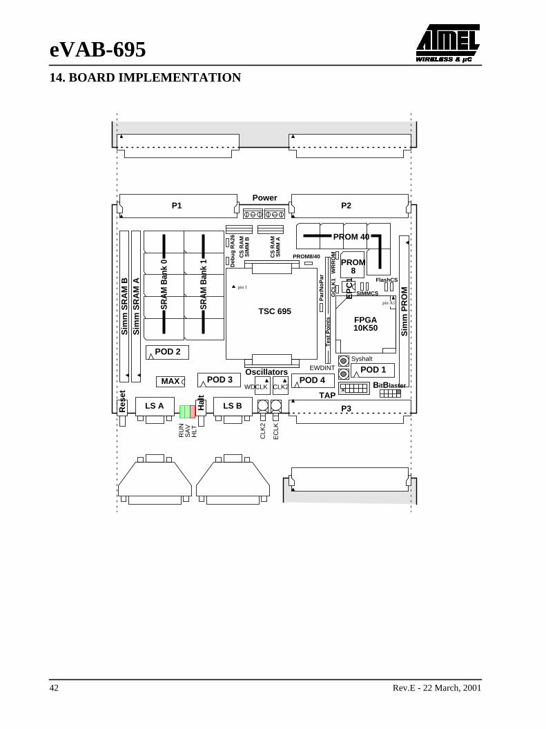
14. BOARD IMPLEMENTATIONPROM 40
EWDINT
PROM8
Sim
m S
RA
M B
Sim
m S
RA
M A
Sim
m P
RO
M
POD 1
POD 2
POD 4POD 3
LS A LS B P3
P2P1
TSC 695FPGA
EP
C1
BitBlaster
TAP
Hal
t
Res
et
PowerH
LT
RU
NS
AV
CLK
2
EC
LK
10K50
Syshalt
OscillatorsMAX
SR
AM
Ban
k 0
pin 1
pin A1
PROM8/40
Par
/NoP
arT
est P
oint
sW
RR
OM
GC
LK1 FlashCS
Deb
ugR
A26
CS
RA
M
CS
RA
MS
IMM
B
SIM
M A
SR
AM
Ban
k 1
WDCLK CLK2
SIMMCS
42 Rev.E - 22 March, 2001
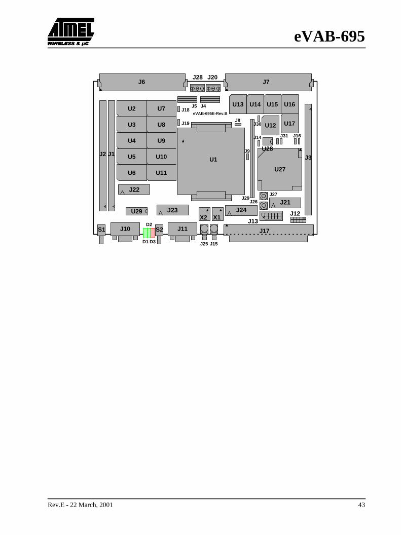
eVAB-695
J26
U12
J2 J1 J3
J21
J22
J24J23
J10 J11 J17
J7J6
U1
U27
U28
J12J13
S2S1
D3D1
D2
J25 J15
J27
X1U29
J8
J9
J29
J30
J14 J16
U2
U3
U4
U5
U6
U7
U8
U9
U10
U11
U17
U16U15U14U13
J28
J5 J4
J19
J18
J20
X2
eVAB-695E-Rev.B
J31
Rev.E - 22 March, 2001 43
eVAB-695
e other
,
15. DEVIATIONS
15.1. CB[6:0] and DPAR on FPGA
The signals CB[7:0] and DPAR connected on FPGA are those of the TSC695 and not those buffered for thspace than SRAM. Note that data connected to FPGA are, effectively, those coming from data buffers.
==> No space protected by EDAC or by Parity can by mapped in FPGA.
15.2. RESET and HALT driven by JTAG connector
The "Reset in" and "HALT in" (from JTAG con to FPGA or CPU) are not possible.
==> If these functions are needed, use the 2x n.c pins of the JTAG connector and connect them to FPGA
pins AD5 and AD6 ("open").
15.3. TSC695 Signals on FPGA
Note that the following signals are missing:
- TMODE[1,0] (not useful)
- DDIR* (but DDIR exits)
- ROMWRT* (on board pulldown)
- DEBUG
- MDS*
- NOPAR*
==> Be careful.
44 Rev.E - 22 March, 2001
eVAB-695
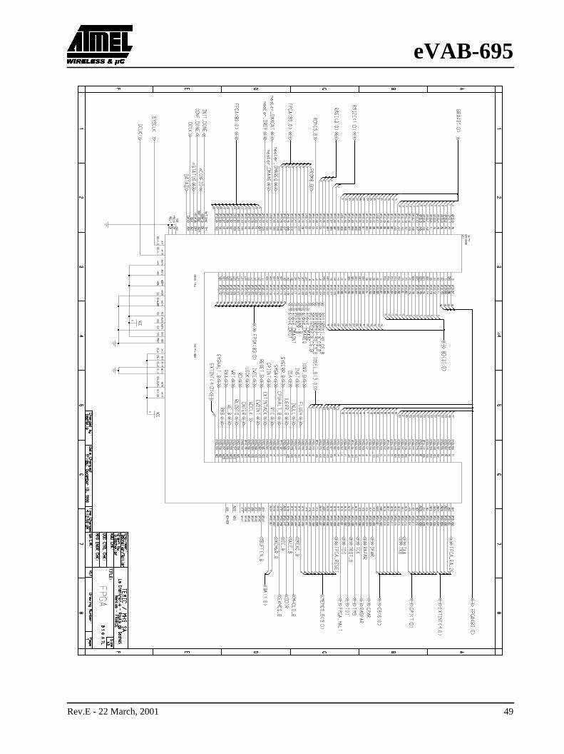
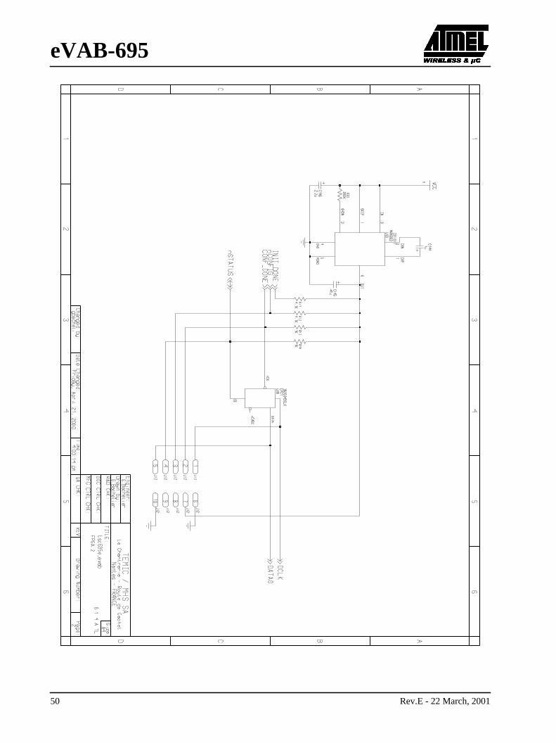
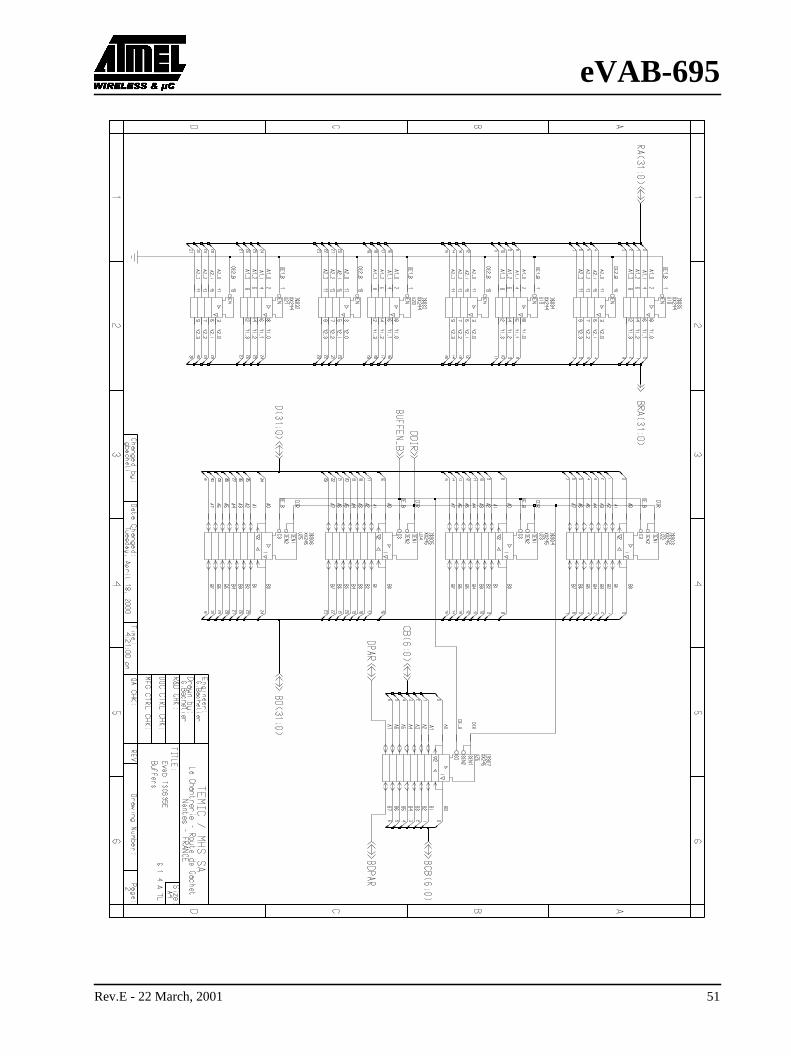
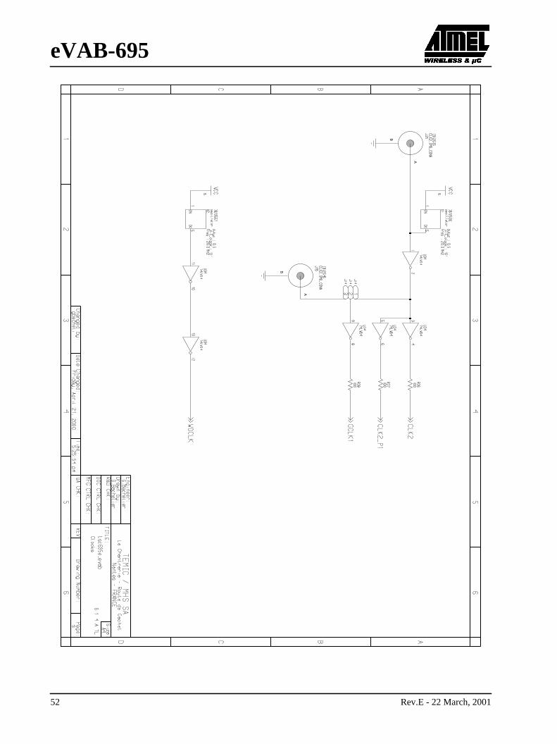
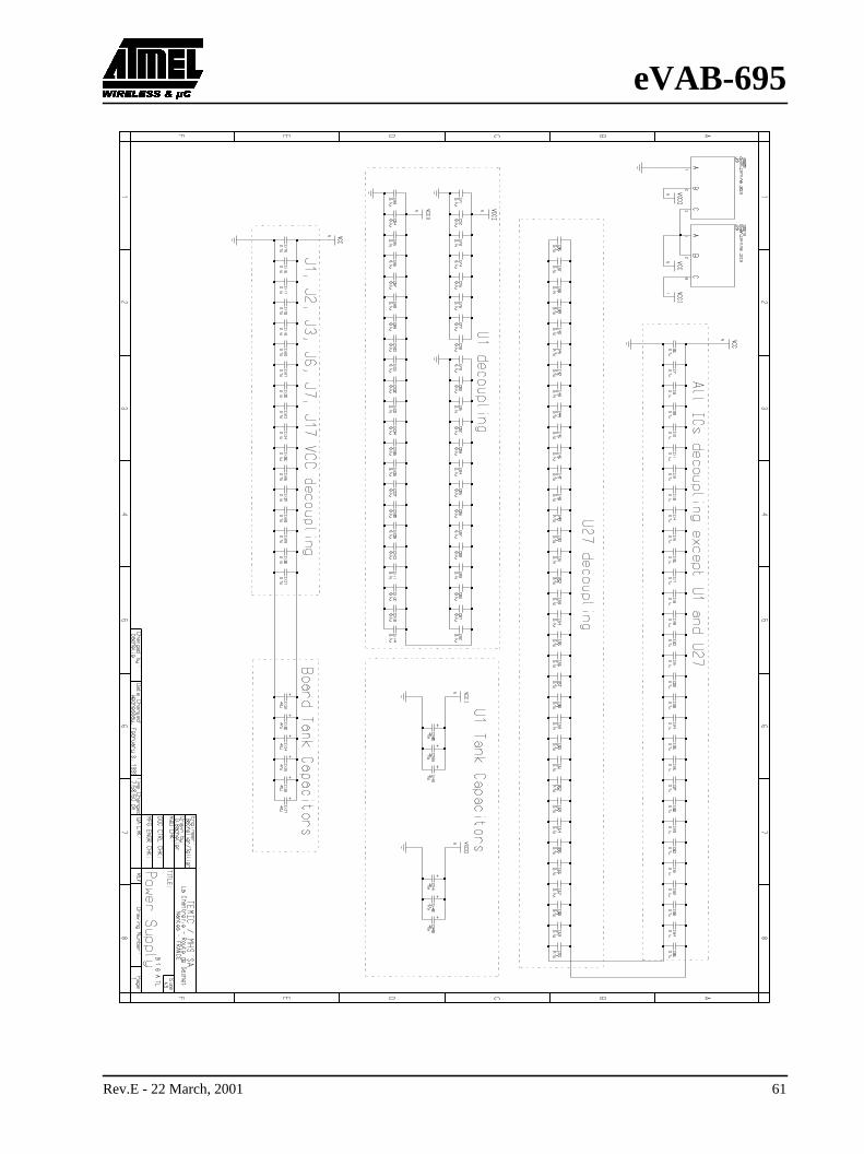
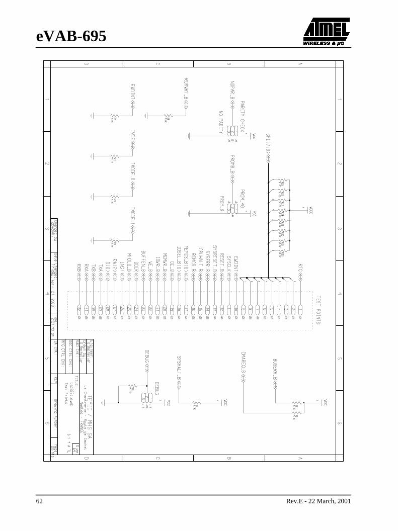
16. SCHEMATICSRev.E - 22 March, 2001 45
eVAB-695
46 Rev.E - 22 March, 2001
eVAB-695
Rev.E - 22 March, 2001 47
eVAB-695
48 Rev.E - 22 March, 2001
eVAB-695
Rev.E - 22 March, 2001 49
eVAB-695
50 Rev.E - 22 March, 2001
eVAB-695
Rev.E - 22 March, 2001 51
eVAB-695
A
B
A
B
52 Rev.E - 22 March, 2001
eVAB-695
B
A
Rev.E - 22 March, 2001 53
eVAB-695
54 Rev.E - 22 March, 2001
eVAB-695
A
B
Rev.E - 22 March, 2001 55
eVAB-695
56 Rev.E - 22 March, 2001
eVAB-695
Rev.E - 22 March, 2001 57
eVAB-695
58 Rev.E - 22 March, 2001
eVAB-695
Rev.E - 22 March, 2001 59
eVAB-695
60 Rev.E - 22 March, 2001
eVAB-695
Rev.E - 22 March, 2001 61
eVAB-695
62 Rev.E - 22 March, 2001
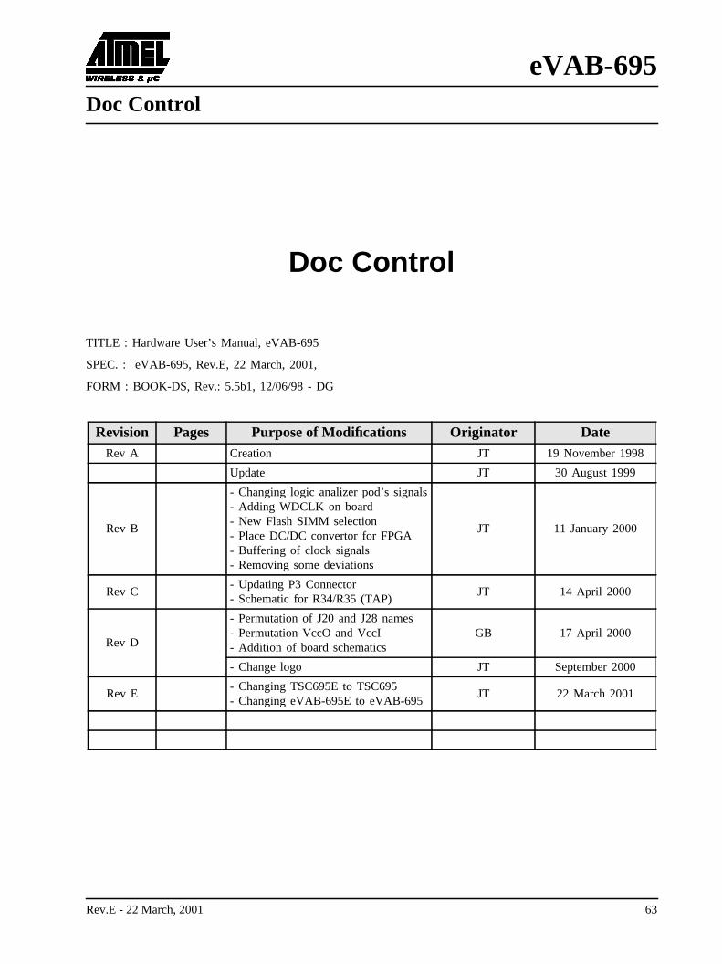
eVAB-695
Doc ControlDoc Control
TITLE : Hardware User’s Manual, eVAB-695
SPEC. : eVAB-695, Rev.E, 22 March, 2001,
FORM : BOOK-DS, Rev.: 5.5b1, 12/06/98 - DG
Revision Pages Purpose of Modifications Originator DateRev A Creation JT 19 November 1998
Update JT 30 August 1999
Rev B
- Changing logic analizer pod’s signals- Adding WDCLK on board- New Flash SIMM selection- Place DC/DC convertor for FPGA- Buffering of clock signals- Removing some deviations
JT 11 January 2000
Rev C- Updating P3 Connector- Schematic for R34/R35 (TAP)
JT 14 April 2000
Rev D
- Permutation of J20 and J28 names- Permutation VccO and VccI- Addition of board schematics
GB 17 April 2000
- Change logo JT September 2000
Rev E- Changing TSC695E to TSC695- Changing eVAB-695E to eVAB-695
JT 22 March 2001
Rev.E - 22 March, 2001 63

eVAB-695
Notes 1:64 Rev.E - 22 March, 2001
eVAB-695
Notes 2:Rev.E - 22 March, 2001 65

eVAB-695
Notes 3:66 Rev.E - 22 March, 2001

eVAB-695
Notes 4:Rev.E - 22 March, 2001 67
eVAB-695
Notes 5:68 Rev.E - 22 March, 2001