harnessing vlsi system design with eda tools - springer978-94-007-1864-7/1.pdf · vlsi laboratory...
TRANSCRIPT

Harnessing VLSI System Design with EDA Tools

Rajanish K. Kamat • Santosh A. Shinde Pawan K. Gaikwad • Hansraj Guhilot
Harnessing VLSI System Design with EDA Tools

Rajanish K. KamatDepartment of ElectronicsVLSI LaboratoryShivaji [email protected]
Pawan K. GaikwadDepartment of ElectronicsVLSI LaboratoryShivaji [email protected]
Santosh A. ShindeDepartment of ElectronicsVLSI LaboratoryShivaji [email protected]
Hansraj GuhilotDepartment of ElectronicsVLSI LaboratoryShivaji [email protected]
ISBN 978-94-007-1863-0 e-ISBN 978-94-007-1864-7DOI 10.1007/978-94-007-1864-7Springer Dordrecht Heidelberg London New York
Library of Congress Control Number: 2011938274
© Springer Science+Business Media B.V. 2012No part of this work may be reproduced, stored in a retrieval system, or transmitted in any form or by any means, electronic, mechanical, photocopying, microfilming, recording or otherwise, without written permission from the Publisher, with the exception of any material supplied specifically for the purpose of being entered and executed on a computer system, for exclusive use by the purchaser of the work.
Printed on acid-free paper
Springer is part of Springer Science+Business Media (www.springer.com)

Dr. Rajanish K. Kamat was born in India in 1971. He received B.Sc. in Electronics, M.Sc. in Electronics both in distinction in 1991 and 1993 respectively. Further he completed M.Phil. in Electronics in 1994 and qualified the State Eligibility Test (in 1995), which is mandatory for faculty positions in India. He pursued his Ph.D. in Electronics specialized in ‘Smart Temperature Sensors’ at Goa University and completed the same in 2003. He was awarded merit scholarship during the Masters programme.Dr. Kamat is currently an Associate Professor with the Department of
Electronics, Shivaji University, Kolhapur, India. Prior to joining Shivaji University, he was working for Goa University and on short term deputation under various faculty improvement programmes to Indian Institute of Science, Bangalore and IIT Kanpur. He has successfully guided five students for Ph.D. in the area of VLSI Design. His research interests include Smart Sensors, Embedded Systems, VLSI Design and Information and Communication Technology. He is recipient of the Young Scientist Fellowship under the fast track scheme of Department of Science and Technology, Government of India and extensively worked on Open Source Soft IP cores. One of his research papers won 4th place in the international paper contest organized by American Society for Information Science and Technology [ASIST, USA] for the year 2008. He has published over 35 research papers, presented over 60 papers in conferences and authored three books: Unleash the System On Chip using FPGAs and Handel C (U.K., Springer, 2009), Practical Aspects of Embedded System Design using Microcontrollers C (U.K., Springer, 2008), Exploring C for Microcontrollers: A Hands on approach (U.K., Springer, 2007).Dr. Kamat is a Member of IEEE and also a life member of Society of
Advancement of Computing. He has been listed in the Marquis Who’s Who in the World, USA.

Dr. Santosh A. Shinde was born in India in 1981. He received B.Sc. in Electronics, M.Sc. Electronics both in First Class in 2004 and 2006 respectively. Further he completed his Ph.D. specialized in VLSI Design in the year 2009. Currently he is working as an Assistant Professor at Department of Electronics, Shivaji University, Kolhapur. He has published over 10 research papers, presented over 06 papers in conferences and authored two books: Unleash the System On Chip using FPGAs and Handel C (U.K., Springer, 2009), Practical Aspects of Embedded System Design using Microcontrollers C (U.K., Springer, 2008) both published by Springer, UK.
Dr. Gaikwad Pawan Kumar was born in India on August 29, 1976. He did his M.Sc. from University of Poona, Pune. He further pursued specialized programmes in the areas of VLSI design and Cyber Law. He completed his Doctorate in Electronics from Shivaji University, Kolhapur for which he developed FPGA based Portable ECG and Pulse Oximeter. The significant part of his research work has been reported in the present book.

Prof. Hansraj Guhilot was born in Haraji, Rajasthan, India in 1958. He received B.E. in Electronics from University Visveswaraiah College of Engineering, Bangalore and M.Tech in Industrial Electronics from Karnataka Regional Engineering College, Surathkal in 1981 and 1985 respectively in first class with distinction.Presently he is Professor and Head in the Department of Electronics and
Communication in K.L.E. Society’s College of Engineering & Technology, Udyambag, Belgaum, He has to his credit 26 years of rich professional experience that includes two years consultancy for a US based company. He holds 9 interna-tional and 1 Indian patents. His areas of interests are Smart Sensors, Agro-Electronics, Biomedical and Mixed Mode VLSI Design. He is as an expert in Power Electronics especially his patented solution on a power processor for metal halide lamps and High Frequency Electronic Ballast for lighting has been major breakthroughs in the industry. He has published 27 research papers and was felicitated by Ministry of Human Resource Development, Govt. of India, for owning international patents.Prof. Guhilot is a fellow of Institute of Electronics & Telecommunication
Engineers and Indian Society for Lighting Engineers and member of Indian Society for Technical Education and IEEE. He has been listed in Indo American Who’s Who and Asian American Who’s Who.

ix
One of the most challenging disciplines in this era of increasing consumerism, shrinking design cycles, lowered project budget without compromising the perfor-mance is undoubtedly the Very Large Scale Integration a.k.a. VLSI. In order to address the increasing owes of the chip designers with respect to the above men-tioned attributes, the phenomenal growth of Electronic Design Automation i.e. EDA is witnessed in the present decade. The EDA regarded as the main arm of the today’s’ VLSI has successfully set a track record of four decades by now, and still is witness-ing many challenges, which is witnessed by the good number of research groups all over the globe. The present book “Harnessing VLSI System Design with EDA Tools” is yet another endeavor placed in front of the chip designers by a group of experienced research professionals.When more and more designers opting for the Field Programmable Gate Array
(FPGA) as their realization platform, the induction of the books as the present one is very apt and therefore, I foresee that it will be well taken up by the design commu-nity. The fundamental aspect of the book is sharing the research experiences of the authors’ with the design community, which I liked the most. Such sort of efforts would definitely bring the laboratory technologies to market and foster the ties between the industries and academia. Another appreciable facet of the book is the adoption of the mixed EDA techniques pertinent to the design problems. For instance the authors have used VHDL, Handel C and Verilog to exemplify the appropriate choice of the tools fitting to the complexity and nature of the systems to be designed. The book instead of focusing on mere theoretical discussion encourages hands on aspects and harps on realization of the systems in the FPGA paradigm. The docu-mentation style of the book is also research oriented which is not a surprise as al the authors have had their stint in research and have come out with three such books prior to the present one besides many research papers in the journals of high repute.In my opinion, the book will be a value addition and may be viewed from differ-
ent perspective by the potential readers. The Post Graduate Science and Engineering students might found it useful to learn the design cycle right from the problem defi-nition, using appropriate methodology to attack the problem and coming out with a successful project design. Nevertheless, the research professionals like doctorate
Foreword

x Foreword
students will find it useful to derive parallel case studies for defining their research topics. Networking professionals’ interested in designing smart appliances with internet connectivity will be benefited with the know-how reported here as regards to the system design with highest level of abstraction. The biomedical community may take up product design with focus on the portability aspects. The soft IP cores reported in one of the chapters are really useful for any designer to comprehend their systems by merely analytical marriage of the pre-designed, thoroughly verified design blocks. The time-to-digital converter reported in the last chapter is really a boon for alleviating the power hungry ADCs required in almost all the SoCs today.Thus in nutshell, the book will serve the EDA and chip design community well
and it will be sort of lamp post for the professionals nurturing their career in this domain of knowledge where the rate of obsolescence is really awesome.
Prof. (Dr.) A.D. Shaligram Prof. (Dr.) G.M. NaikProfessor and Head Professor and HeadDepartment of Electronic Science Department of ElectronicsUniversity of Pune Goa UniversityPune GOA

xi Foreword
Prof. (Dr.) A.D. Shaligram is presently professor and Head, Department of Electronic Science, University of Pune. His research interests are Optoelectronics, Fiber optic and Optical Waveguide sensors, PC/Microcontroller based Instrumentation, Simulation software development, Biomedical Instrumentation and sensors. He has successfully guided many Doctorate students in the area VLSI design and completed research, development and consultancy projects in the above mentioned areas. Dr. Shaligram has been instrumental in standardization of the Electronics course material and inspired fellow colleagues to inculcate innovations in teaching and research techniques.
Prof. (Dr.) G.M. Naik is presently Professor and Head, Department of Electronics, Goa University, Goa. He did his Doctorate from Indian Institute of Science, Bangalore. At Goa University Prof. Naik has successfully launched the teaching and research programme in the areas of VLSI Design with the grant-in-aid from University Grants Commission under Innovative Scheme. He is an active researcher in VLSI Design and has been instrumental to nurture quality Human Resource in this area.


xiii
Preface
The dictionary meaning of the word ‘Harness’ is ‘to bring under conditions for effective use’ or ‘gain control over for a particular end’ and in view of that the title of the book “Harnessing VLSI System Design with EDA Tools” itself intuitive enough in the VLSI arena. It aims at exploring the various dimensions of the EDA techno logies for achieving different goals of the VLSI system design. The EDA has by now matured enough with its longstanding stint of more than four decades of existence and is constantly evolving along with its other contemporary comple-menting technologies such as the computing architectures, algorithms, data mining techniques and not to stop thinking about the FPGAs which have revolutionized the VLSI system design aspects through fast prototyping. Though, the scope of the EDA in a true sense is very broad and comprises of the diversified hardware and software tools to accomplish different phases of the VLSI system design such as design, layout, simulation, testability, prototyping or implementation, however this book focuses only on demystifying the code a.k.a. firmware development and its implementation in the FPGA paradigm. In fact there are different varieties of such languages empowering the EEs for attaining their system design goals; none-theless through this book we put forth our notion of FPGA based system design through a variety of case studies selected from different engineering domains and realized through different languages.Before the readers start with this book, we would like to caution them about the
very nature of the book. This is not a text book unlike our earlier ones Unleash the System On Chip using FPGAs and Handel C (U.K., Springer, 2009), Practical Aspects of Embedded System Design using Microcontrollers C (U.K., Springer, 2008), Exploring C for Microcontrollers: A Hands on approach (U.K., Springer, 2007). After reading our previous book on Handel C, many EEs wrote to us that we should now deliver something in greater depth with live case studies for truly perceiving the feel of applications. This has really motivated us to shape the present book. Authors would like to specially mention about good books on EDA, VLSI Design and FPGAs (mentioned in [20–31] in reference section) and our book is no

xiv Preface
way attempts to be substitute for these books. Instead it is a value addition by focusing on the research aspects in VLSI Design.After setting the background of the book, we would now like to mention about
its key features. The book is written by the researchers for the budding researchers. The different chapters present the gist of the research work which has led the authors to their doctorate degree. Mainly two types and three languages viz. Hardware Description Languages (VHDL and Verilog) and Behavioral High-Level Languages (Handel C) have been used for developing the firmware. The prototyp-ing environment used is the Xilinx FPGAs and it is worth mentioning here that the Xilinx Starter Kit was very useful for testing and prototyping. We assume the readers of this book to be familiar with Digital Electronics, Computer Networking, Algorithms and Computational theory and also with the basic design flow pertain-ing to the FPGA based design projects. Covering these aspects in one text is fairly impossible and worthless. Instead we have provided footnotes pointing to the refer-ence through which the readers can gather more information. The text also presents practical know-how of the state-of-art design methodologies such as ‘Hardware-Software Codesign’, ‘Soft IP Cores’ and so on. It also presents the complete listing of the code so that any one who is interested can further use these soft IP cores in their design projects. The screenshots and device utilization reports are purposely given in depth so that the readers could make themselves familiar with the design for testability and debugging aspects. The reference/bibliography section at the end of the book is quite rich and lists around 170 selected references drawn from the scholarly journals, industry whitepapers, web resources and presentations of various researchers.Finally we would like to give a brief about the organization of the book. The
book is divided into five chapters.Chapter 1 introduces the theme of the book and covers the very rationale behind
proposing this book. The major conclusion which is on the basis of the research papers of visionaries in the field like ‘Makimoto’ and ‘Tredennick’ is the emerging need of the state-of-art VLSI applications to have mixed mode design environments. The book then takes this further in two ways. First, it exemplifies development of FPA based applications with different language suits like VHDL, Verilog and System C. Second, even while building these case studies the issues such as testability, verification, power consumption etc. have been handled again by using different sets of EDA tools such as ModelSim, Leonardo Spectrum etc.Chapter 2 starts with an interesting application of developing FPGA based Anti-
Spam solution which comes from the reported processing bandwidth limitations of general purpose processors, which can serve only a few hundred Mbps throughput which then poses a bottleneck in the overall bandwidth of the setup. Hardware based Anti-Spam solution has been projected as the potential solution to alleviate the bandwidth holdups. Amongst the hardware based solutions, the FPGAs offer the most striking advantages due to their inherent capability to reconfigure; offer more throughputs and exploit parallelism. Moreover, with the development of the tools such as Handel C that work at the higher level of abstractions, their programming

xvPreface
becomes easy. The anti-spam solution described in this chapter derives benefits of all the constructive attributes of the FPGA based system design that includes hardware-software codesign, integration of the soft IP cores on the chip and proto-typing the entire functionality on a single platform reducing the off-chip access cycles to minimum possible. With careful grasping of the chapter details, a design environment that allows networking experts to use FPGAs might also be explored for many similar problems.Chapter 3 presents yet another interesting application in the biomedical / health
care domain. The casse study described here deals with design of low-cost, minia-ture, lightweight, low-power, portable ECG system. Such wearable health monitoring systems integrated into a telemedical system are a promising new information tech-nology capable to support prevention and early detection of abnormal conditions. The portable system developed during the present research work is capable of recording, storing and real time displaying the ECG in a single portable device. For emergency detection the analysis can incorporate patients profile and activity infor-mation to reduce the number of false alarms. The main advantage of the deve-lopment is the cardiologist can gather data from the patient over a long period of time, during which the patient can enjoy their normal day-to-day lifestyle. The sys-tem is very useful because the ECG signals obtained from stress examinations are diagnostically important in detecting a number of heart diseases, which may not be apparent when the patient is at rest. Goal of this development is to determine the ‘normal’ state of the patient in different activity modes so that each set of ECG read-ings may then be interpreted within the context of the patient’s current physical activity. The research work also addresses the issue of today’s most pressing matters in medical care i.e. response time to patients in need. It suggests a FPGA based solution with a support of VHDL that would help reduce response time in emer-gency situations utilizing modem based trans-receiving technology.Chapter 4 provides a comprehensive overview of developing FPGA based
embedded and discuss how FPGAs have the potential to be used as a platform for System-on-Chip (SoC) styled designs. The firmware developed and implemented in the form of soft IP cores showcases the manner in which such cores can be combined to form semicustom ASICs for the intended applications. The soft IP cores reported here, if reused judiciously might lead to big solutions for the development problems of the potential readers of this book.A widely agreed fact is that for any modern applications A to D converter is
unavoidable. However integrating such a ADC poses several typical problems due to its inherent mixed mode architecture. Time to Digital Converter a.k.a ‘time interval measurement’ have traditionally been popular with the discrete digital components. In Chap. 5 we have developed such as high precision ADC based on vernier Time to Digital conversion principle. Again he we rely on Verilog for the firmware part and Spartan 3e FPGA for prototyping.Thus in nutshell the book shares an integrated knowledge based of the authors’
and the value addition comes from their research background. It is hoped that the integrated presentation of information, with embellishment using expounding case

xvi Preface
studies, will be of value to many readers looking out to develop their research problems. Authors’ hope that the text will stimulate further innovations and would really lookforward to hear from the readers regarding the usefulness of the text.
Dr. Rajanish K. KamatDr. Santosh A. ShindeDr. Pawan K. GaikwadProf. Hansraj Guhilot

xvii
There are so many people, whose support, encouragement & inspiration are very much essential to accomplish major achievements in life, especially, if it involves the elements of fulfilling one’s cherished dreams such as publishing this fourth quality book through Springer. For me, this book is such an important destiny & I am indeed, indebted to lot of people for their well wishes & blessings, for completing this journey. This book infact is a compiled version of the cumulative knowledge and wisdom gained throughout the research work of the authors’ towards their doctoral work at the Department of Electronics, Shivaji University, Kolhapur which is on the dawn of entering into its golden jubilee year.At the outset we extend our sincere thanks to Springer, through which we could
reach good number of Institutes of Higher Learning all over the globe. It is really gratifying to notice through the Online Catalogue of Library of Congress and Google Book tools that our previous three books have find their appropriate place in the leading Libraries in the world and also referred in the curricula of worldclass institutes. This wouldn’t been possible without the editorial support of the editors and the Springer staff with whom we work for last three years. We would like to pace on record our sincere appreciation towards Charles B. Glaser, Senior Editor, Electrical Engineering and Elizabeth Dougherty as well as Mark de Jongh and Ms. Cindy Zitter for their persuasion and patience through the project.We are highly indebted to our present Vice-Chancellor Prof. (Dr.) N.J. Pawar and
the past Vice-Chancellor Prof. (Dr.) M.M. Salunkhe for motivating, guiding, and helping us to complete this project. The book would not have been possible without the encouragement, wisdom, feedback, and support from Dr. G.M. Naik, Professor and Head, Department of Electronics, Goa University and Dr. A.D. Shaligram, Professor and Head of Pune University who has also kindly agreed to give foreword to this book. Thanks are also due to Department of Science and Technology (DST), New Delhi for using the facilities procured through the DST Fast Track Young Scientist Project granted to Dr. R.K. Kamat.
Acknowledgments

xviii Acknowledgments
Special thanks to our family members who were enthusiastic towards our writing. Moreover, Dr. Kamat would like to dedicate his contribution in this text to his new born daughter “Reva”.It is well known that in the writing of any text, the person who benefits is the
author himself. We think this is true in our case too. We dedicate this work to all those who have directly or indirectly helped and encouraged us.
Dr. Rajanish K. KamatDr. Santosh A. ShindeDr. Pawan K. GaikwadProf. Hansraj Guhilot

xix
1 Introduction ............................................................................................... 1 1.1 Introduction ...................................................................................... 1 1.2 Prologue ........................................................................................... 1 1.3 EDA: From Methodologies, Algorithms,
Tools to Integrated Circuits and Systems......................................... 2 1.4 EDA from Halcyon’s Days to the Blooming
Paradigm of Chip Industry ............................................................... 4 1.5 Categories of the EDA Tools ........................................................... 5 1.6 Quo Vadis, EDA? The Challenges and Opportunities ..................... 6 1.7 Just One More Book on EDA or Value
Addition to the Scholarly Literature by US? ................................... 8 1.8 Designing the System as SoC Using the Soft IP Cores ................... 9 1.9 Types of IP Cores ............................................................................. 101.10 Design Issues Pertaining to the Soft IP Cores ................................. 111.11 Justifying FPGA as the Prototyping Platform ................................. 111.12 Justifying the Differing Flavors of Languages
Used in This Book ........................................................................... 14
2 Development of FPGA Based Network on Chip for Circumventing Spam ........................................................... 15 2.1 Introduction ...................................................................................... 15 2.2 Conception of the Spam Mail .......................................................... 16 2.3 FPGA Based Network on Chip for Circumventing Spam ............... 18
2.3.1 Inspiration ............................................................................ 182.3.2 Core Concept ....................................................................... 182.3.3 Method ................................................................................. 182.3.4 Motivation ............................................................................ 192.3.5 Advantages of FPGA Based Antispam
Appliance in Nutshell .......................................................... 192.3.6 Significance of the Work ...................................................... 20
Contents

xx Contents
2.4 Tools Infrastructure and Design Flow .............................................. 21 2.4.1 Handel C .......................................................................... 21 2.4.2 ISE Webpack 9.2 .............................................................. 22 2.4.3 EDK Version 9.2 .............................................................. 22 2.4.4 Xilinx Starter Kit ............................................................. 23
2.5 Introducing Hardware-Software Co-design ..................................... 23 2.6 Hardware Software Co-design ......................................................... 24
2.6.1 Motivation for Hw/Sw Co-design .................................... 25 2.6.2 Advantages of Hw/Sw Co-design Methodology ............. 26 2.6.3 State of the Art Hw-Sw Co-design Methodologies ......... 26
2.7 Hardware-Software Codesign Framework Proposed in the Present Case Study ............................. 28 2.7.1 Addressing the Issues Through Co-design ...................... 29
2.8 Description of System at Higher Level ............................................ 30 2.9 Resolving the System a Step Down ................................................. 302.10 System Design ................................................................................. 31
2.10.1 Microblaze Processor ....................................................... 33 2.10.2 PLB BUS ......................................................................... 33 2.10.3 XPS UART Lite ............................................................... 35 2.10.4 Off Chip Level Converter ................................................ 35 2.10.5 XPS Ethernet Lite ............................................................ 35 2.10.6 SMSC LAN83C185 High Performance
Single Chip Low Power 10/100 Mbps Ethernet Physical Layer Transceiver (PHY) .................... 36
2.10.7 XPS Timer ....................................................................... 36 2.10.8 XPS Interrupt Controller .................................................. 37 2.10.9 Double Data Rate (DDR) Synchronous
DRAM (SDRAM) Controller .......................................... 372.10.10 Off Chip DDR SDRAM MT46V32M16 ......................... 39
2.11 Development of Soft IP Core of Bloom Filter ................................. 39 2.11.1 Justifying Bloom Filters for the Keyword Parsing .......... 39 2.11.2 Theoretical Foundations of Bloom Filter......................... 40 2.11.3 Hash Function .................................................................. 40 2.11.4 Deciding the Size and Number of Hash
Functions in Our Bloom Filter Implementation .............. 422.12 Presenting System Design of Purely Software Modules ................. 452.13 Integrating of the Hardware-Software Modules Using EDK .......... 472.14 Setting the POP3 Client and Describing
Overall Working of the System........................................................ 472.15 Conclusion ....................................................................................... 49
3 Analog Front End and FPGA Based Soft IP Core for ECG Logger ............................................................................... 51 3.1 Prior Art ........................................................................................... 51 3.2 The Very Rationale of the System ................................................... 53

xxiContents
3.3 Analog Front End of the Setup ........................................................ 54 3.3.1 Leads Formation ................................................................ 54 3.3.2 Restricting Number of Leads ............................................. 54 3.3.3 ECG Instrumentation Amplifier ........................................ 56 3.3.4 Deriving the Signal from the Augmented Leads ............... 56 3.3.5 Filtering the ECG Signal ................................................... 60 3.3.6 Multiplexing the Lead Signals ........................................... 62 3.3.7 Post-multiplexer Amplifier Stage ...................................... 62 3.3.8 Digitization of the ECG Signal .......................................... 62 3.3.9 FPGA Based Handshake Micro-logic................................ 633.3.10 MODEM Interface ............................................................. 63
3.4 VHDL Implementation of the ECG Soft IP Core ............................ 65 3.4.1 Driving ADC: LTC 1407 and Storing
Data in 3D RAM ................................................................ 65 3.4.2 Details of the VHDL Code ................................................ 69 3.4.3 VHDL Processes for Conversion and Storage
in 3D Memory: (Process P_conv, P_SHIFT and P_STORE) .................................................................. 69
3.4.4 VHDL Process for Serial Transmission of the ECG Signal (Process Serial) .................................... 71
3.5 ModelSim Simulation Results ......................................................... 71 3.6 Synthesis Results Using Mentor Graphics Tool:
Leonardo Spectrum .......................................................................... 73 3.6.1 Synthesis Report ................................................................ 73 3.6.2 RTL View ........................................................................... 76 3.6.3 Technology Schematic View.............................................. 76 3.6.4 Critical Path Schematic ...................................................... 76
3.7 Monitoring the ECG Using MODEM Based Setup ........................ 76 3.7.1 Tele-monitoring of the ECG
Signal at the Hospital End ................................................. 76 3.8 ECG Signal Reconstruction Mechanism
at the Hospital End ........................................................................... 76 3.8.1 DAC Interfacing Details .................................................... 78 3.8.2 FPGA Driving Demultiplexer and DAC:
Core Algorithm .................................................................. 79 3.8.3 Serial ECG Receiver: Flow Chart ...................................... 81
3.9 VHDL Listing for Driving the Analog Demultiplexer and Serial DAC from Spartan-3E FPGA ......................................... 81
3.10 Discussion Regarding the VHDL Implementation .......................... 833.10.1 Process Serial_P ................................................................. 833.10.2 Process S_OUT .................................................................. 84
3.11 ModelSim Simulation Results ......................................................... 843.12 Synthesis Results Using Mentor Graphics Tool:
Leonardo Spectrum .......................................................................... 853.12.1 Synthesis Report ................................................................ 853.12.2 RTL View ........................................................................... 86

xxii Contents
3.12.3 Technology Schematic View.............................................. 903.12.4 Critical Path Schematic ...................................................... 90
3.13 Conclusion ....................................................................................... 90
4 FPGA Based Multifunction Interface for Embedded Applications ...................................................................... 93 4.1 Introduction ...................................................................................... 93 4.2 Universal FPGA Based Interface for High
End Embedded Applications ........................................................... 94 4.2.1 Hardware Aspects ................................................................ 94
4.3 Soft IP Core for the LCD Interface .................................................. 95 4.4 Soft IP Core for the DAC Interface ................................................. 100 4.5 Handel C Listing of the Soft IP Core
for the DAC Interface ...................................................................... 101 4.6 Soft IP Core for the Linear Tech LTC6912-1
Dual Amp Interface ......................................................................... 106 4.7 Soft IP Core for the ADC Interface ................................................. 108 4.8 Soft IP Core for the VGA Interface ................................................. 113 4.9 Soft IP Core for the Keyboard Interface .......................................... 1174.10 Triangular Wave Generator Using DAC .......................................... 1224.11 Conclusion ....................................................................................... 126
5 FPGA Based High Resolution Time to Digital Converter ..................... 127 5.1 Introduction ...................................................................................... 127 5.2 TDC: Prior Art ................................................................................. 128 5.3 TDC Using Vernier Principle ........................................................... 129
5.3.1 Coarse measurement .......................................................... 130 5.3.2 FINE MEASUREMENT ................................................... 133
5.4 Simulation and Verilog Modules ..................................................... 137 5.4.1 Ring Oscillator (Fast Clock) RTL Schematic .................... 139 5.4.2 Verilog Module for Ring Oscillator (Fast Clock) .............. 139 5.4.3 Verilog Module for Ring Oscillator (Slow Clock) ............. 140 5.4.4 Phase Detector ................................................................... 142 5.4.5 Simulation Wave Form of Phase Detector ......................... 142 5.4.6 Verilog Module for 8 Bit Counter ...................................... 142 5.4.7 RTL Schematic of 8 Bit Counter ....................................... 143 5.4.8 Simulation Results of 8 Bit Counter .................................. 143 5.4.9 Verilog Module for 8 Bit Counter ...................................... 1445.4.10 RTL Schematic of Time to Digital Converter .................... 1445.4.11 Schematic of Time to Digital Converter ........................... 1455.4.12 Verilog Module for Time to Digital Converter .................. 145
5.5 Applications of the TDC Implemented ............................................ 146
References ........................................................................................................ 147

xxiii
Fig. 1.1 Typical constituents of an EDA tool indicating an underlying interdisciplinary knowledge base ............................ 3
Fig. 1.2 Increasing VLSI complexities forcing the evolution of the EDA ............................................................... 8
Fig. 1.3 Comparison of the types of IP cores .............................................. 10
Fig. 2.1 Characteristics of spam emails ....................................................... 18Fig. 2.2 Motivation for co-design methodology .......................................... 25Fig. 2.3 Our framework for hardware-software codesign ........................... 30Fig. 2.4 Higher level schematic of the system ............................................ 31Fig. 2.5 Functional architecture of the system ............................................ 32Fig. 2.6 System design ................................................................................ 32Fig. 2.7 Base configuration of the DDR SDRAM ....................................... 38Fig. 2.8 Memory interface details revealed by EDK ................................... 38Fig. 2.9 Round robin arbitration algorithm shown by EDK ........................ 38Fig. 2.10 Hash function mapping variable length
keywords to fixed length vector ...................................................... 41Fig. 2.11 Variation of false positive rate as a function of m/n....................... 44Fig. 2.12 Variation of size of bloom filter
as a function of the error rate ......................................................... 44Fig. 2.13 Varying value of false positive as a function
of number of hash functions .............................................................. 45Fig. 2.14 Variation of false positive with number
of hash functions at a given m/n ratio ............................................ 45Fig. 2.15 Figure revealing the role of LWIP stack in the system .................. 46Fig. 2.16 Design flow for the Xilinx EDK
adopted in the present work ........................................................... 48
List of Figures

xxiv List of Figures
Fig. 3.1 The three standard leads form an equidistant triangle (Einthoven triangle) ........................................ 55
Fig. 3.2 (a) Lead-I: (LA–RA), (b) Lead-II: (LL–RA), (c) Lead-III: (LL–LA), (d) aVL: {LA – (RA + LL)/2}, (e) aVR: {RA – (LA + LL)/2}, and (f ) aVF: {LL – (RA + LA)/2} .................................................. 57
Fig. 3.3 Wilson network and right leg drive ................................................ 60Fig. 3.4 Six lead ECG data acquisition system using FPGA ...................... 61Fig. 3.5 LTC1407 operating sequence (Retrieved from Linear
Technology Corpo ration: LTC1407 data sheet) ............................. 63Fig. 3.6 (a) Flow diagram to drive serial ADC LTC1407
using FPGA and (b) flow diagram to drive serial ADC LTC1407 using FPGA .......................................................... 64
Fig. 3.7 Flow diagram shows how to transmit the serial data bits of a 15 bit data frame ....................................... 66
Fig. 3.8 A three dimensional memory structure used in VHDL code ........................................................ 70
Fig. 3.9 Simulation window to show driving of serial ADC and generating serial data for transmission .......................... 72
Fig. 3.10 RTL view of the system ADC driver and serial transmitter ...................................................................... 74
Fig. 3.11 Technology schematic view of the system ADC driver and serial transmitter .................................................. 75
Fig. 3.12 Critical path view of the system ADC driver and serial transmitter ........................................................... 77
Fig. 3.13 ECG signal reconstruction mechanism at the hospital end .......................................................................... 78
Fig. 3.14 Timing diagram of the DAC LTC1257 (Retrieved from the Linear Technology Corporation data sheet) .................................................................. 78
Fig. 3.15 A 15 bits data frame receiving serially .......................................... 79Fig. 3.16 Flowchart to drive analog demultiplexor
and serial DAC from spartan 2e FPGA .......................................... 80Fig. 3.17 Simulation results of VHDL code
for ECG receiver driver .................................................................. 85Fig. 3.18 RTL view of the ECG serial receiver ............................................. 87Fig. 3.19 Technology schematic view
of the ECG serial receiver .............................................................. 88Fig. 3.20 Critical path view of the ECG serial receiver ................................ 89Fig. 3.21 Snapshot of the setup ..................................................................... 90
Fig. 4.1 Hardware design of the universal FPGA based interface .............. 95Fig. 4.2 Top level view of the soft IP core for the LCD .............................. 96Fig. 4.3 Detailed synthesis view of the soft IP core for the LCD ............... 96Fig. 4.4 Top level synthesis view of the DAC interface .............................. 101

xxvList of Figures
Fig. 4.5 Top level synthesis view of the VGA interface .............................. 114Fig. 4.6 Detailed synthesis view of the VGA interface ............................... 115
Fig. 5.1 Basic principle of measurement of time interval using Nutt Interpolation method .............................................................. 130
Fig. 5.2 Selecting a DCM from clocking wizard ........................................ 131Fig. 5.3 General setup wizard for DCM as a frequency multiplier ............. 132Fig. 5.4 Wizard shows specifying the clock buffers to be used .................. 132Fig. 5.5 DCM used as a symbol in schematic design entry ........................ 133Fig. 5.6 Behavioral simulation of frequency multiplier .............................. 133Fig. 5.7 Editable floor plan for ring oscillators ........................................... 133Fig. 5.8 Schematic and behavioral simulation of error finder ..................... 134Fig. 5.9 Timing for the slow clock, fast clock ............................................. 135Fig. 5.10 General block diagram revealing the principle .............................. 136Fig. 5.11 Schematic of double ring oscillator with start, stop control .......... 136Fig. 5.12 Editable floor plan for ring oscillators ........................................... 137Fig. 5.13 Ring oscillator timing simulation................................................... 137Fig. 5.14 Schematic and behavioral simulation of phase detector ................ 138Fig. 5.15 Ring oscillator timing simulation................................................... 140Fig. 5.16 Schematic of the ring oscillator for fast clock configuration ......... 141Fig. 5.17 Schematic of phase detector ........................................................... 141Fig. 5.18 Behavioral simulation of phase detector ........................................ 142Fig. 5.19 RTL schematic of 8 bit counter Fig. 5.20 Simulation results ....... 143Fig. 5.20 Simulation results........................................................................... 143Fig. 5.21 RTL schematic of TDC .................................................................. 144Fig. 5.22 Final schematic of the TDC ........................................................... 145

xxvii
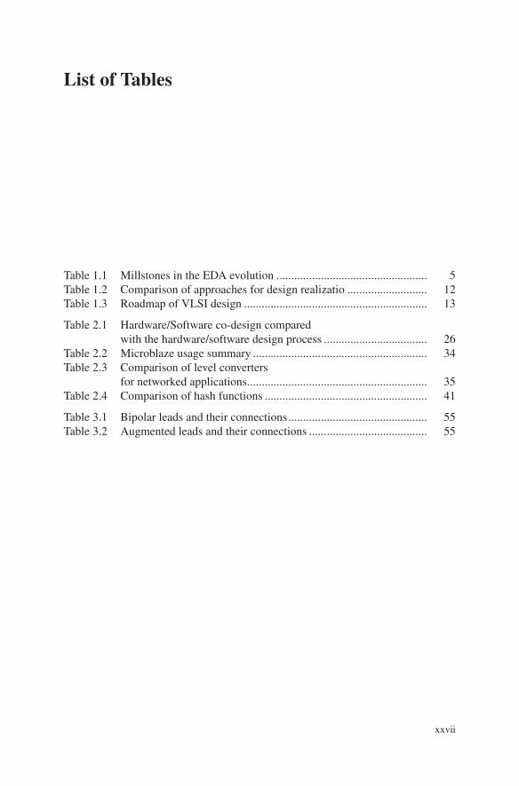
List of Tables
Table 1.1 Millstones in the EDA evolution ................................................... 5Table 1.2 Comparison of approaches for design realizatio ........................... 12Table 1.3 Roadmap of VLSI design .............................................................. 13
Table 2.1 Hardware/Software co-design compared with the hardware/software design process ................................... 26
Table 2.2 Microblaze usage summary ........................................................... 34Table 2.3 Comparison of level converters
for networked applications ............................................................. 35Table 2.4 Comparison of hash functions ....................................................... 41
Table 3.1 Bipolar leads and their connections ............................................... 55Table 3.2 Augmented leads and their connections ........................................ 55
