helsinki university of technologylib.tkk.fi/dipl/2006/urn007322.pdf · helsinki university of...
TRANSCRIPT

HELSINKI UNIVERSITY OF TECHNOLOGYDepartment of Ele tri al and Communi ations EngineeringLaboratory of Ele troni s Produ tion Te hnologySusanna AuraPro essing of inorgani -organi hybridmaterial for mi rouidi appli ations
Thesis for the degree of Master of S ien e in Te hnology.Espoo, August 7th 2006Supervisor: Professor Jorma KivilahtiInstru tor: Do ent Sami Franssila

Prefa eThis work was done at the Mi roele troni s entre of Helsinki university of te h-nology. The Mi ronova building provided ex ellent fa ilities to do the master'sthesis.First, I would like to thank Professor Jorma Kivilahti from laboratory of ele -troni produ tion te hnology for supervising this thesis. I would also like to thankthe laboratory of ele troni produ tion te hnology for giving me the opportunityto use their fa ilities for ell adhesion tests. My gratitude also goes to, do entSami Franssila, for giving me the opportunity to do my master's thesis at Mi- roele troni s entre. I would also like to thank him for his ideas and feedba kthroughout the work. My thanks also go to all of my o-workers at Mi roele -troni s entre for the pleasant working atmosphere and for all the help they havegiven me.Finally, I would like to thank my family and friends for their love and support.Espoo, 17 July 2006Susanna Aura
ii

HELSINKI UNIVERSITY OF ABSTRACT OF THE MASTER THESISTECHNOLOGYAuthor: Susanna AuraName of the thesis: Pro essing of inorgani -organi hybrid materialfor mi rouidi appli ationsDate: 7.8.2006 Number of pages: 66Department: Ele tri al and Communi ations EngineeringProfessorship: S-113 Bioadaptive te hnologySupervisor: Prof. Jorma KivilahtiInstru tors: Do ent Sami FranssilaMi rosystem te hnology and as a part of it mi rouidi is a fast growing eld ofte hnology, whi h produ es e.g mi ros ale analysis devi es for analyti al hem-istry. Traditionally sili on and glass have been used for mi rouidi devi e fabri- ation, but polymers are gaining ground mainly due to their easy pro essing.In this master's thesis a new inorgani -organi hybrid polymer, ORMOCER r©, ispresented and its properties are evaluated from mi rouidi point of view. Com-mer ially available ORMOCER r©material alled ORMOCOMP r©has been usedthroughout this thesis. Both UV-lithography and UV- embossing were testedto produ e stru tures. The tests showed that ORMOCOMP is extremely UV-sensitive and for this reason fabri ation of small, 100 µm stru tures is di ult.However, smaller stru tures an be produ ed by using a lter to redu e the inten-sity of the maskaligner. If the stru ture size is under 20 µm, the UV-embossingshould be used sin e in this method the exposure dose is less riti al.The bonding pro ess for en losed hannel fabri ation has been developed. Thiste hniques provides an easy and reprodu ible bonding. Chemi al stability and ell adhesion of ORMOCOMP r©were also studied. The hemi al stability ofORMOCOMP proved to be relatively good, and it showed non-toxity in elladhesion tests.Keywords: ORMOCER, mi rouidi iii

TEKNILLINEN KORKEAKOULU DIPLOMITYÖN TIIVISTELMÄTekijä: Susanna AuraTyön nimi: Epäorgaaninen-orgaanisen hybridimateriaalinprosessointi mikrouidistisiin sovelluksiinPäivämäärä: 7.8.2006 Sivuja: 66Osasto: Sähkö- ja tietoliikennetekniikkaProfessuuri: S-113 Bioadaptiivinen tekniikkaTyön valvoja: Prof. Jorma KivilahtiTyön ohjaajat: Dosentti Sami FranssilaMikrosysteemitekniikan yhtenä osa-alueena mikrouidistiikka on nopeasti kehit-tyvä teknologia, joka tuottaa mm. erilaisia mikrokokoluokan analyysilaitteita ana-lyyttisen kemian tarkoituksiin. Perinteisiä materiaaleja mikrouistiikassa ovatolleet pii ja lasi, mutta erilaiset polymeerimateriaalit ovat valtaamassa alaalähinnä niiden prosessoinnin helppouden vuoksi.Tämä diplomityö esittelee uuden epäogaanisen-orgaanisen hybridi polymeerin,ORMOCER r©in ja tarkastelee sen ominaisuuksia mikrouidististen sovellus-ten kannalta. Kaupallisesti saatavilla olevaa ORMOCER materiaalia, ORMO-COMPia, on käytetty tähän diplomityöhön tehdyissä tutkimuksissa. Sekä UV-litograaa että UV-embossingia on käytetty rakenteiden valmistamiseen. Tehdyttestit osoittivat että ORMOCOMP on UV herkkä materiaali ja tästä syystä pien-ten, alle 100 µm rakenteiden valmistus on hankalaa. Pienempien rakenteidentuottaminen on kuitenkin mahdollista käyttäen suodatinta valotuslaitteen inten-siteetin vähentämiseksi. Mikäli halutaan valmistaa alle 20 µm rakenteita, on syytäkäyttää UV-embossingia, koska säteilyannos on tassä menetelmässä vähemmänkriittinen.Kanavien sulkemiseksi on kehitetty bondausmenetelmä, joka tarjoaa helpon jatoistettavan bondauksen. ORMOCOMP r©in kemiallista stabiilisuutta ja soluad-heesiota siihen on myös tutkittu. ORMOCOMP r©osoittautui kemiallisesti kohta-laisen stabiiliksi ja lisäksi se todistettiin myrkyttömäksi soluadheesiotesteissä.Avainsanat: ORMOCER, mikrouidistiikkaiv

Contents1 Introdu tion 12 Pattern transfer 32.1 UV-lithography . . . . . . . . . . . . . . . . . . . . . . . . . . . . 42.1.1 Photoresists . . . . . . . . . . . . . . . . . . . . . . . . . . 42.2 Imprint te hniques . . . . . . . . . . . . . . . . . . . . . . . . . . 62.2.1 Elastomeri stamp fabri ation . . . . . . . . . . . . . . . . 82.2.2 Step and ash imprint lithography . . . . . . . . . . . . . 103 ORMOCER r©s 143.1 Stru tural units and network forming rea tions . . . . . . . . . . . 143.2 Material properties . . . . . . . . . . . . . . . . . . . . . . . . . . 173.2.1 Me hani al and thermal properties . . . . . . . . . . . . . 183.2.2 Opti al and ele tri al properties . . . . . . . . . . . . . . . 183.3 Photopolymerization . . . . . . . . . . . . . . . . . . . . . . . . . 193.4 Appli ations of ORMOCER r©s . . . . . . . . . . . . . . . . . . . 203.4.1 Ele tri al and opti al appli ations . . . . . . . . . . . . . . 203.4.2 Prote tive and de orative oatings . . . . . . . . . . . . . . 213.4.3 Dental appli ations and other medi al appli ations . . . . 224 Pro essing parameters 25v

4.1 UV-lithography pro ess . . . . . . . . . . . . . . . . . . . . . . . . 254.1.1 Surfa e pretreatment . . . . . . . . . . . . . . . . . . . . . 264.1.2 Resist deposition . . . . . . . . . . . . . . . . . . . . . . . 264.1.3 Soft bake . . . . . . . . . . . . . . . . . . . . . . . . . . . 274.1.4 Exposure . . . . . . . . . . . . . . . . . . . . . . . . . . . 284.1.5 Hard bake . . . . . . . . . . . . . . . . . . . . . . . . . . . 304.1.6 Development . . . . . . . . . . . . . . . . . . . . . . . . . 314.1.7 Final bake . . . . . . . . . . . . . . . . . . . . . . . . . . . 314.2 UV-moulding pro ess . . . . . . . . . . . . . . . . . . . . . . . . . 324.2.1 Stamp fabri ation . . . . . . . . . . . . . . . . . . . . . . . 335 Stability and adhesion tests 375.1 Chemi al stability . . . . . . . . . . . . . . . . . . . . . . . . . . . 385.2 Conta t angle measurements . . . . . . . . . . . . . . . . . . . . . 385.3 Cell adhesion . . . . . . . . . . . . . . . . . . . . . . . . . . . . . 405.3.1 Substrate patterning . . . . . . . . . . . . . . . . . . . . . 405.3.2 Cell ulture . . . . . . . . . . . . . . . . . . . . . . . . . . 415.3.3 Sample preparation . . . . . . . . . . . . . . . . . . . . . . 415.3.4 SEM analysis . . . . . . . . . . . . . . . . . . . . . . . . . 426 Fluidi hip fabri ation 446.1 Bonding methods . . . . . . . . . . . . . . . . . . . . . . . . . . . 446.2 Fabri ation of en losed ORMOCER mi ro hannels . . . . . . . . 466.3 Inlet fabri ation . . . . . . . . . . . . . . . . . . . . . . . . . . . . 497 Con lusions 51Referen es 53vi

AbbreviationsBHF Buered hydrouori a idCERAMER Cerami polymerCNP Combined nanoimprint and photolithographyDLC-PDMS Diamond-like arbon poly(dimethyl siloxane)EBL Ele tron beam lithographyEUV Extreme ultravioletHF Hydrouori a idHMDS HexamethyldisilazaneIC Integrated ir uitICP-RIE Indu ed oupled plasma rea tive ion et hingNIR Near infra redORMOCER Organi ally modied erami ORMOSIL Organi ally modied sili atePAC Photoa tive omponentPBS Phosphate buered salinePC Poly arbonatePDMS Poly(dimethyl siloxane)PMMA Polymethylmeta rylateRIE Rea tive ion et hingrpm Rotations per minuteSFIL Step and ash imprint lithographyUV Ultraviolet
vii

Chapter 1Introdu tionMi rosystem te hnology and, as a part of it, mi rouidi s are rapidly growingand developing elds. This relatively new te hnology has adapted most of itsfabri ation te hniques from semi ondu tor te hnology. Along with these dier-ent te hniques the most used material in semi ondu tors, sili on, has long beenthe ore of mi rosystem te hnology as well. However, in re ent years new mate-rials have gained ground espe ially in mi rouidi appli ations. One often usedmaterial in analyti al hemistry equipment is glass and for this reason its use inmi roanalysis systems has been broadly studied espe ially for on- hip apillaryele trophoresis [1, 2. Even though glass has some good properties, for exampleit is hemi ally stable, the mi ropro essing of glass is di ult whi h makes itsuse somewhat impra ti al. One of the most attra tive material lass in today'smi rouidi is polymers. Their easy pro essability and low pri e make themappealing materials [3. The use of polymeri material has also led to develop-ment of totally new fabri ation te hniques, whi h provide both high throughputand resolution patterning. Major drawba k of polymers is typi ally their poorthermal and hemi al stability. For example often used polymer, poly(dimethylsiloxane) (PDMS) is not stable in onta t with some organi solvents and at hightemperatures [4.In mid 1980's two independent groups reported on the preparation of new sol-gelbased materials, inorgani -organi hybrids. Wilkes termed them as CERAMERs( erami polymers) [5 and S hmidt named these materials rst as ORMOSILs1

CHAPTER 1. INTRODUCTION 2[6, 7, 8, organi ally modied sili ates, but he later hanged the name to OR-MOCERs, organi ally modied erami s, to emphasize their erami properties.In some arti les dieren e between organi -inorgani and inorgani -organi poly-mers have been made. Inorgani -organi polymers have inorgani elements intheir main hain and organi side groups. If their inorgani ba kbone is formedvia traditional sol-gel pro essing of modied metal alkoxides and that is followedby organi ross-linking the resulting hybrid materials are alled ORMOCERs.On the other hand, if the main hain ontains arbon atoms and some inorgani side groups, they are alled organi -inorgani polymers [9. However this kindof ategorization has not been well established and usually no dieren e is madebetween terms inorgani -organi and organi -inorgani polymer.ORMOCER r©s ombine properties from several dierent material lasses. Pro- essing of ORMOCER is easy due to its polymeri nature. But at the sametime it does not suer from the same problems as typi al polymers be ause ofits inorgani network. ORMOCERs' easily modied properties have made themappealing material in dierent appli ations. ORMOCERs have been used as pro-te tive oatings, in mi ro-opti appli ations and as lling materials in dentistry.Their use in mi rouidi appli ations have not yet been evaluated.The main part of this thesis deals with the properties of ORMOCER and pro ess-ing of mi rouidi hannels from it. Chapter 2 gives the ba kground knowledgeabout dierent fabri ation pro esses and hapter 3 on entrates on the materialitself. In the experimental part the optimal pro essing parameters for mi rouidi hannel fabri ation are presented for two dierent pro esses; UV-lithography andUV-moulding. In hapter 5 the use of ORMOCER in mi rouidi appli ationsis evaluated by testing its hemi al stability. Some ell adhesion tests were alsomade. Finally in hapter 6 the en losed hannel fabri ation is des ribed. Thisbonding te hnique utilizes the polymerization properties of ORMOCER and leadsto tight seal between bonded layers.

Chapter 2Pattern transferThere are several ways to transfer patterns onto dierent substrates. Lithographyis a standard pro ess, whi h utilizes photoresist and -mask. Mi rolithography isthe ore te hnology of semi ondu tor devi e fabri ation [10.Over the years the need for smaller linewidth and better resolution has led touse of shorter wavelengths. Dierent photolithographi systems an be divideda ording to their wavelengths. These in lude opti al or ultraviolet (UV)-, deep-UV-, extreme-UV (EUV) and X-ray lithographies. Deep-UV uses 248/193/157nmwavelength, where as EUV and X-ray utilize 13nm and 6-40nm, respe tively.Even though shorter wavelength leads to better resolution, there are some prob-lems, whi h have so far prevented more extensive use of espe ially EUV and X-raylithography. For instan e ree tive elements have to be repla ed with multi-layer(Bragg) mirrors. Also with every redu tion of wavelength the resist and maskmaterials used have to be redesigned. For these reasons opti al lithography is stillthe most used method in resear h laboratories as well as in volume produ tion.Opti al lithography will be dis ussed in more detail in the next se tion.Alongside with onventional lithography many new fabri ation methods, oftenreferred to soft lithography [11, have been developed. These te hniques usuallyutilize some kind of stamp to form stru tures and they provide heap and sim-ple fabri ation pro ess. Some of these te hniques are dis ussed in forth omingse tion. 3
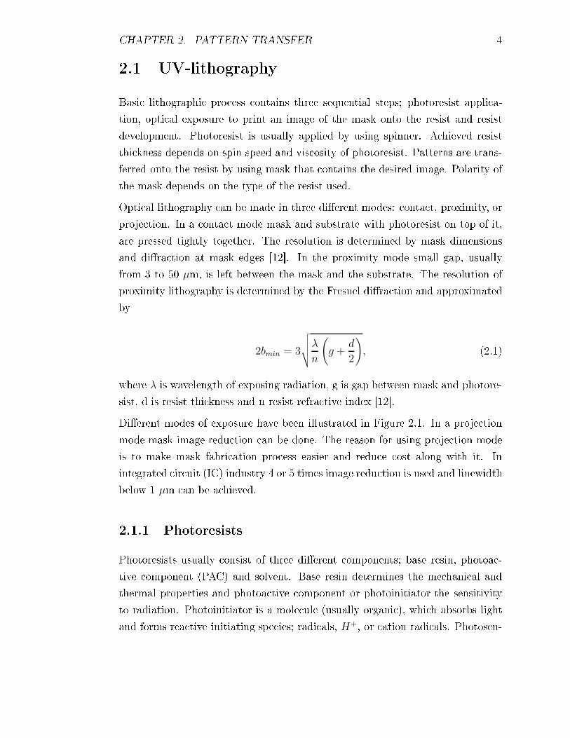
CHAPTER 2. PATTERN TRANSFER 42.1 UV-lithographyBasi lithographi pro ess ontains three sequential steps; photoresist appli a-tion, opti al exposure to print an image of the mask onto the resist and resistdevelopment. Photoresist is usually applied by using spinner. A hieved resistthi kness depends on spin speed and vis osity of photoresist. Patterns are trans-ferred onto the resist by using mask that ontains the desired image. Polarity ofthe mask depends on the type of the resist used.Opti al lithography an be made in three dierent modes: onta t, proximity, orproje tion. In a onta t mode mask and substrate with photoresist on top of it,are pressed tightly together. The resolution is determined by mask dimensionsand dira tion at mask edges [12. In the proximity mode small gap, usuallyfrom 3 to 50 µm, is left between the mask and the substrate. The resolution ofproximity lithography is determined by the Fresnel dira tion and approximatedby2bmin = 3
√
√
√
√
λ
n
(
g +d
2
)
, (2.1)where λ is wavelength of exposing radiation, g is gap between mask and photore-sist, d is resist thi kness and n resist refra tive index [12.Dierent modes of exposure have been illustrated in Figure 2.1. In a proje tionmode mask image redu tion an be done. The reason for using proje tion modeis to make mask fabri ation pro ess easier and redu e ost along with it. Inintegrated ir uit (IC) industry 4 or 5 times image redu tion is used and linewidthbelow 1 µm an be a hieved.2.1.1 PhotoresistsPhotoresists usually onsist of three dierent omponents; base resin, photoa -tive omponent (PAC) and solvent. Base resin determines the me hani al andthermal properties and photoa tive omponent or photoinitiator the sensitivityto radiation. Photoinitiator is a mole ule (usually organi ), whi h absorbs lightand forms rea tive initiating spe ies; radi als, H+, or ation radi als. Photosen-

CHAPTER 2. PATTERN TRANSFER 5
Figure 2.1: Dierent modes of UV-lithography.sitizers are also sometimes used. Photosensitizer is a mole ule, whi h has theability to absorb energy and transfer it to photoinitiator. Solvents are used to ontrol the vis osity of the photoresists. Vis osity has dire t impa t on a hievedlayer thi kness. Problems may arise if the vis osity of the photoresist is highbe ause it will ow on an uneven surfa e resulting non-uniform layer thi kness.Resist materials have to full some requirements in order to be useful. For ex-ample they have to be hemi ally and me hani ally stable so that they an beused in forth oming pro esses. These in lude et hing and ion implantation inwhi h resist a ts as a mask material. Resist sensitivity an be altered to dierentwavelengths. Sensitivity is import for produ tivity. [12Photoresists an be divided into two ategories; positive and negative resists. Oneof the most used positive photoresist is Novala , whi h is insoluble in developersprior to exposure. Its photoa tive omponent a ts to inhibit the dissolution of theNovala resin. Upon exposure photoa tive omponent de omposes and releases arboxyli a id, whi h makes the exposed resist soluble in the developer solution,whi h are usually dilute alkaline solutions.On the other hand in negative photoresist, su h as SU-8, unexposed areas areremoved after exposure. Photoa tive omponent of SU-8 rea ts with UV-lightand atalyses the ross-linking rea tion, whi h ontinues in post exposure bake.After the post-bake, un ured areas are removed with suitable solvent. In Figure2.2 the operation of negative and positive photoresists are illustrated.

CHAPTER 2. PATTERN TRANSFER 6
Figure 2.2: Operation of positive and negative photoresists.2.2 Imprint te hniquesLight wavelength redu tion has traditionally been the method for a hieving betterresolution [13, but as mentioned before shorter wavelength brings some additionalproblems. Dierent fabri ation methods that are based on ele tron beam anprodu e high resolution patterns but they suer from low throughput. Imprintte hniques were developed to provide high resolution and throughput patterning.There are many imprint lithography te hniques, all having the same basis. Thebasi idea is to use stamp together with some uring pro ess to pattern thesurfa e.Imprint lithography te hniques an be divided into two ategories, UV- and tem-perature -based methods, depending on the uring pro ess used. In tempera-ture based method, usually referred to hot embossing, used polymer is warmedabove its glass transition temperature and the stamp is pressed in onta t withpolymer lm using high for e. For ommonly used thermoplasti materials likepolymethylmeta rylate (PMMA) or poly arbonate (PC) this temperature is inthe range of 100-180C. The embossing for e is typi ally of the order of 20-30kN [14 and it is held for few minutes. While still applying the for e, both thestamp and the substrate are ooled to just below the glass transition temperatureof the substrate. After that the stamp is deta hed from the patterned surfa e.Hot embossing pro ess and its temperature and pressure y les are presented inFigure 2.3.

CHAPTER 2. PATTERN TRANSFER 7
Figure 2.3: S hemati drawing of hot embossing pro ess(left) and temperatureand pressure y les. [15Commonly used stamp materials in hot embossing are sili on and ni kel. Repli- ation errors may arise due to a mismat h between thermal expansion oe ientof polymer and that of the stamp material. Typi al values for the thermal ex-pansion oe ient of polymers are of the order of 7x10⁻⁵/K, while for sili on itis 2.6x10⁻⁶/K and for ni kel 1x10⁻⁵/K. For this reason the thermal y le of thepro ess should be as small as possible. S hemati drawing of the hot embossingequipment is presented in Figure 2.4.In UV-based te hniques, UV light is used to ure polymer lm. In this methodneither high pressure nor high temperature is needed. In UV - embossing [16either transparent stamp or substrate is needed in order to perform photopoly-merization. In ase of a non-transparent stamp, ba kside illumination has to beused. In this se tion prin iples of UV-based te hniques are examined. Also sin efeature sizes are highly dependent on stamp used, their fabri ation is dis ussedin detail.

CHAPTER 2. PATTERN TRANSFER 8
Figure 2.4: S hemati drawing of the hot embossing equipment. [142.2.1 Elastomeri stamp fabri ationStamps an be either elastomeri or some harder material for example sili onor quartz. Elastomeri stamps are widely used due to their good properties ompared with ommon, hard, stamps. Due to their elasti ity they, for example, onform to dierent substrates.The most ommonly used material in elastomeri stamps is poly(dimetyl siloxane)(PDMS) [17. PDMS has several properties whi h make it a good material forhigh-quality pattern and stru ture formation. PDMS onforms to the surfa eof the substrate and it is released relatively easily. Due to its low interfa ialfree energy, it does not adhere irreversibly to or rea t with the polymers beingmoulded.Even though there are several advantages of using exible, elastomeri stamps,exibility also brings some di ulties. Pairing is a problem that o urs whenaspe t ratio of relief stru tures is too large. Delamar he et al. showed that theaspe t ratios (l/h, Figure 2.5a) of the relief stru tures on PDMS surfa e had to bebetween about 0.2 and 2 in order to obtain defe t-free stamps [18. Sagging o urswhen features in the stamp are widely separated (d ≥ 20h, Figure 2.5b). Alsoshrinking of PDMS during uring an lead into di ulties. Figure 2.5 illustratesthese problems.

CHAPTER 2. PATTERN TRANSFER 9
Figure 2.5: Deformation of elastomeri stamp. a)Pairing, b)sagging, )shrinking[11In Figure 2.6b basi steps of a fabri ation of elastomeri stamp are shown. First amaster is prepared using some lithographi te hnique (Figure 2.6a). The hoi e ofthe fabri ation method for the master depends on the desired feature size. Usuallymaster an be fabri ated using onventional UV-lithography, but if smaller, under200 nm, stru tures are needed, the ele tron beam lithography (EBL) an be used.EBL provides high resolution but due to its low throughput it an not be used inmass produ tion. Master material is usually sili on be ause of its well establishedfabri ation pro ess.When the master has been fabri ated, the stamp an be prepared by astingthe liquid prepolymer of an elastomer against the master. The master, withun ured prepolymer on top, is then put into va uum, so that all the air bubblesare removed from the elastomer. Then the prepolymer is ured for a period oftime that depends on a temperature used. Temperatures between 20 C and80 C an be used while the time required varies between 24 hours to 1 hour.Cured elastomer is peeled o the master. The same master an be used morethan 50 times [11. This is one of the advantages of UV-molding sin e fabri ation

CHAPTER 2. PATTERN TRANSFER 10of the master is slow espe ially if EBL is used. Coating of the master an alsoextend its lifetime. In one study the SU-8 master was oated with amorphousdiamond-like arbon-poly(dimethylsiloxane) hybrid (DLC-PDMS-h) lm [19. Itwas shown that while un oated SU-8 master ould be used only for one or twoPDMS asting, the oated one showed no degradation of SU-8 or DLC-PDMS-h oating after ten PDMS repli ation. Another oating method for master is to usea thin teon-like lm [20 as an anti-adhesive layer. This layer is deposited byusing ommon rea tive ion et hing (RIE) ma hine. Depending on the feed gases,RIE an be used either for et hing or for polymeri lm deposition. For teon-likelm deposition CHF3 an be used as feed gas. Fluorine-to- arbon ratio shouldbe near two, but be ause there are hydrogen moieties present they will rea twith surplus uorine produ ing HF. In this way the ratio will be approximately2. The same kind of thin teon-like lm has been used to oat ni kel stamp forhot embossing pro ess [21. As shown in Table 2.1 the surfa e energy of ni kel ishigh, whi h auses problems of adhesion between surfa es. Teon-like lms arethe most used oatings to redu e this adhesion.
Figure 2.6: (a) Fabri ation of hard, sili on stamp or master. (b)Fabri ationpro ess of elastomeri stamp. [112.2.2 Step and ash imprint lithographyOne relatively new imprint te hnique is step and ash imprint lithography (SFIL).In this te hnique photopolymerization hemistry and low pro essing pressure is

CHAPTER 2. PATTERN TRANSFER 11Table 2.1: Properties of dierent stamp materialsSi Ni kel Quartz PDMS SU-8Density (g/cm3) 2.33 8.9 2.6 0.97 1.2Thermal expansion oe ient (ppm/C) 2.6 13 0.5 310 [22 52Young's Modulus (GPa) 190 (111) 200 76 3*10−3[17 4[23Surfa e energy (mJ/m2) 48 1900 980 21.6 43.6[24used to transfer patterns onto a substrate. The method diers from other im-print te hniques by using a photo urable low vis osity organosili on liquid andtransparent, rigid template [25. The template is fused sili a, where patternsare fabri ated by using ele tron-beam exposure. Due to its transparen y, thelayer-by-layer alignment is possible.Liquid pre-polymer is dispensed onto the surfa e of the substrate. The substrate an be polymeri as well due to a low temperature pro ess. The template isbrought into onta t with the pre-polymer, ausing it to spread a ross the sur-fa e and onform to the stru tures dened by the template. UV light is usedto polymerize the pre-polymer, after whi h the template is separated from thesubstrate. Pre-polymer solution must not hange its omposition signi antly be-tween dispensing and imprinting by for example solvent evaporation. Its vis osityhas to be low enough for it to spread over the entire surfa e and to ll stru turesof the template. It should polymerize rapidly during exposure and shrinkage dueto polymerization must be ontrolled. It should also deta hed from templateeasily after polymerization. [25S hemati pro ess ow is presented in Figure 2.7. Last step shows the post-pro essing, whi h onsists of et hing through the thin residual layer of polymerand further et hing through transfer layer using polymer as et h mask.Residual layer that remains after SFIL pro ess an be problemati in some ap-pli ations. Although the SFIL pro ess itself only take few minutes, the residuallayer removal with RIE an in rease the pro ess time relatively long, whi h limitsthe overall throughput. Also the residual layer thi kness an be non-uniform dueto a imprinting onditions or the pattern omplexity. This makes it di ult todetermine the time needed to et h through the residual layer. Et hing too littlewill lead to some remaining residual layer and et hing too mu h will redu e the

CHAPTER 2. PATTERN TRANSFER 12
Figure 2.7: S hemati of the S-FIL pro ess. Modied from[26aspe t ratio of the stru tures.Cheng et al. [27 introdu ed a ombined nanoimprint and photolithography(CNP) patterning te hnique to over ome this residual layer problem. CNP pro- ess steps are illustrated in Figure 2.8. First, a stamp is fabri ated from UVtransparent material, but additional light-blo king metal layer is applied in pro-trusions of the stamp. When the UV exposure is done through the stamp, areas overed with metal layer are not exposured. When the stamp is removed residuallayer still remains, but this time it an be removed with developing solution. Thiste hnique makes an additional residual layer removal with RIE unne essary andshortens the pro essing time. Also, the aspe t ratio of the stru tures does notsuer from this kind of approa h and the aspe t ratio of produ ed stru tures anbe even higher than that on the stamp.

CHAPTER 2. PATTERN TRANSFER 13
Figure 2.8: Main steps of ombined nanoimprint and photolithography pattern-ing. Modied from [27.

Chapter 3ORMOCER r©sORMOCER r©s (ORgani allyMOdied CERami s, registered trademark of Fraun-hoferGesells haft zur Förderung der angewandten Fors hung e.V., Germany) areinorgani -organi hybrid polymers, whi h onsist of inorgani ba kbone and or-gani side groups. Inorgani ba kbone is formed via sol-gel pro ess followed byorgani polymerization or rosslinking. Due to the formation pro ess of ORMO-CERs, their properties are easily modied.ORMOCERs were rst developed to opti al [28 and ele tri al appli ations [29,but their easily adjustable properties have led to appli ations in many dier-ent elds. ORMOCERs ombine several good properties from dierent material lasses. In Figure 3.1 material relationship of ORMOCER is presented. Theyget e.g toughness and good pro essability from organi polymers, hardness and hemi al and thermal stability from glasses and erami s, and elastomeri andsurfa e properties from sili ones. Low pro ess temperature of ORMOCER r©salso enables the use of low ost polymeri substrates.3.1 Stru tural units and network forming rea -tionsORMOCERs are omposed of four dierent stru tural units. All units are on-ne ted via strong ovalent bonds. Stru tural units an be lassied a ording to14

CHAPTER 3. ORMOCER r©S 15
Figure 3.1: Relationship of ORMOCER r©s to sili ones, organi polymers, glassesand erami s. [30their network forming or modifying roles.
Figure 3.2: Stru tural units of inorgani /organi polymer. [9In Figure 3.2 stru tural units of ORMOCER are presented. Pre ursor type 1 isresponsible for formation of inorgani network. Inorgani network of ORMOCERsare formed via lassi al inorgani sol-gel pro ess. This pro ess onsists of two

CHAPTER 3. ORMOCER r©S 16steps hydrolysis and poly ondensation.Hydrolysis:≡ SiOR + H2O →≡ SiOH + ROH (3.1)Poly ondensation:
≡ SiOH + OH − Si ≡→≡ Si − O − Si ≡ +H2O (3.2)≡ SiOH + RO − Si ≡→≡ Si − O − Si ≡ +ROH (3.3)R in the rea tions is either methyl, ethyl or propyl. These rea tions are startedand ontrolled by the addition of water and atalyst to an al oholi solution ofthe pre ursors. Hydrolysis and poly ondensation happen simultaneously, be ausepoly ondensation starts as soon as the rst hydrolyzed spe ies are present [30.The size of these inorgani units an be inuen ed easily by modi ation of poly- ondensation onditions, e.g temperature, atalyst, on entration or solvent. Theper entage value of inorgani network has major ee t on material properties.The higher per entage will lead to higher elasti modulus, thermal and me han-i al stability and lower thermal expansion oe ient and opti al loss in the nearinfrared region (NIR).Pre ursor type 2 modies properties of ORMOCER. These are usually non-rea tive aryl or akryl groups. Changing their per entage will for example modifydensity of the material. Adding aryli fun tions will raise the refra tive index(up to 1.6). On the other hand alkyl or, even better, uorinated alkylgroups willredu e the refra tive index (down to 1.42). [30Pre ursor type 3 is a network onne ting unit. The longer the hain the lower willbe the elasti modulus and higher will be the thermal expansion oe ient. Toa hieve very high transparen y in the NIR the onne ting unit should be partiallyuorinated.Pre ursor type 4 forms the organi network. It has to be hosen onsidering thenal use of ORMOCER. For example in thin lm te hnology easily polymerizegroups like metha ryl or epoxy are needed. On the other hand these groups ausehigher thermal expansion oe ient and opti al loss in the NIR. [31

CHAPTER 3. ORMOCER r©S 173.2 Material propertiesORMOCERs are transparent and show thermoplasti behaviour due to the or-gani network. Be ause of their formation me hanism ORMOCERs are homoge-neous materials. In ele tron mi ros opy and x-ray investigations no phase separa-tion between organi and inorgani moieties was dete ted [30. The onventionalma ros ale omposites have domain size of mi rometer or even millimeter s ale,but in inorgani -organi hybrid materials they are of nanometer range, typi ally1-100 nm [32.As ould be seen in previous se tion, properties of ORMOCER an be modiedby varying rea tion onditions or hanging organi or inorgani groups. Thereforeit is impossible to give exa t numeri al value for example Young's modulus or re-fra tive index, and some number range is used instead. In Table 3.1 some of theseproperties are presented. The properties of ommer ially available ORMOCERmaterial, ORMOCOMP, are also shown.Table 3.1: Properties of ORMOCER (Modied from [9)Property value ommentDensity(g/ m3) 1.1 - 1.6 without llersThermal expansion 50 - 200 without llers oe ient (ppm/C) 18 - 70 with llersThermal from 180 up < 5% weightstability to 400 C loss (TGA)Young's- from 0.013 up high organi /modulus (GPa) polymer ontentto 18,6 high inorgani ontentORMOCERs are dense and non-porous materials. As show in Table 3.1, the den-sity of ORMOCER lies in between 1.1 to 1.6 g/ m3 depending on the stru ture ofORMOCER material. Density of ORMOCER de reases with in reasing amountof organi moieties.Shrinking of ORMOCER during uring is probably the most major drawba k ofORMOCER materials. Shrinkage an be as high as 50% when both solvent re-moval and uring are taking into a ount [30. Shrinking auses problems be ausehigher me hani al stresses are formed whi h will lead to bending and ra king

CHAPTER 3. ORMOCER r©S 18of the ORMOCER layer. This problem an be solved by using (meth)a rylatealkoxysilane based ORMOCERs, whi h suer frommu h less shrinkage than otherORMOCER materials. With these a rylate based ORMOCERs the shrinkage isredu ed to 2-8 vol.%. Also by adding some llers the shrinkage an be redu edeven further. [303.2.1 Me hani al and thermal propertiesVariations in Young's modulus and thermal expansion oe ient between dif-ferent ORMOCER materials are mainly due to dieren es in organi and inor-gani ontents and the spa er-length onne ting the inorgani and organi sites.Young's modulus in reases with in reasing organi rosslinking density and ther-mal expansion oe ient de reases. As expe ted the Young's modulus in reasesas spa er-length de reases. A drasti in rease of Young's modulus from 70 MPato more than 2000 MPa an be dete ted by de reasing the spa er length from20 to 11 atoms onne ting inorgani and organi ross-linking sites [30. Withmodi ation of alkoxysilane pre ursors thermal expansion oe ient an be from50 to 200 ppm/C and by adding some llers the oe ient an be redu ed to 18ppm/C [9.3.2.2 Opti al and ele tri al propertiesORMOCERs are olourless materials whi h show no absorption in the visiblespe trum. ORMOCER is opti ally transparent over the wavelength range from400 nm to 1600 nm and it has refra tive index of 1.52 at 588 nm. Its refra tiveindex an vary from 1.42 up to 1.6 depending on the ORMOCER omposition.It has a very low absorption loss at near infrared region (NIR) at 1310 nm 0.3dB/ m and at 1550 nm a. 1.5 dB/ m. If uorinated ORMOCER is used, theopti al losses an be redu ed even further [33, 28.ORMOCERs are usually highly diele tri materials. Their bulk resistivity isbetween 1013 and 1015Ωcm. For this reason, and be ause of its good adhesionto dierent substrates, ORMOCERs have been used as interlayer diele tri s inele tri al and opti al inter onne tion te hnology [34.

CHAPTER 3. ORMOCER r©S 193.3 PhotopolymerizationTerm photopolymerization means a hain rea tion that is initiated by photo hem-i al event. It diers from photo rosslinking be ause latter one requires photonfor ea h hain propagation step. In photopolymerization every absorbed photonpolymerizes a number of monomer units. This number of monomer units perabsorbed photon is alled quantum yield.Φm =
Rp
Iabs
=Rate of polymerization (inM
s)
Light intensity absorbed (in Einstein 1
ls)
(3.4)Photopolymerization an be divided into two groups; radi al and ationi poly-merization. As an example of ationi photopolymerization is a ring-openingrea tion of epoxies, whereas a rylates are polymerized by radi al rea tion [35.Both of these systems an be initiated by UV light sour e and both require pho-toinitiator. The major dieren e between these two rea tion s hemes omes fromthe dieren es in the hemistry of photoinitiator. Cure speed in free radi al sys-tem is usually higher than in ationi polymerization. In both ases initiationhappens usually through light exposure, but in ationi systems the properties ofthe ured lm are improved by post-thermal treatment.One of the things that need to be onsidered in radi al photopolymerization isoxygen inhibition. Oxygen inhibition o urs in the photoinitiated radi al poly-merization of a rylate resin, whi h is a base monomer of many UV- urable resins.In this rea tion the free radi als formed by the photolysis of the initiator rea twith oxygen mole ules forming peroxyl radi als. Peroxyl radi als are not rea tivetowards the a rylate double bonds and an not therefore initiate or parti ipatein any polymerization rea tion. They usually attra t hydrogen atoms from thepolymer ba kbone to generate hydroperoxides. Inhibition ee t of oxygen on theradi al polymerization of a rylates is more pronoun ed in the top layer of thelm in onta t with the air [36. When the lm thi kness in reases, the inuen eof the oxygen inhibition de reases, sin e the thi kness of the inhibition layer isproximately the same regardless of the lm thi kness. There are dierent pos-sibilities to over ome this usually unwanted rea tion. Probably the most usedmethod is to perform the radi al polymerization under inert gas atmosphere, e.g.

CHAPTER 3. ORMOCER r©S 20in nitrogen gas ow. The bonding pro ess presented in later hapter is based onoxygen inhibition rea tion.3.4 Appli ations of ORMOCER r©sNumerous dierent appli ations utilizing inorgani -organi hybrid materials haveemerged sin e their development. Nowadays appli ations over several dierentelds from mi ro-opti s to dental appli ation. In this se tion some of these ap-pli ations are presented.3.4.1 Ele tri al and opti al appli ationsDue to ORMOCERs good opti al properties, it has been widely used in opti alappli ation. There are few ommer ial ORMOCER materials available; ORMO-CORE and ORMOCLAD from Mi ro resist te hnology. They have been devel-oped for planar opti al waveguiding, ORMOCORE being the ore material andORMOCLAD the ladding material [37.One of the most studied ORMOCER appli ation is its use in mi roopti al om-ponents, su h as gratings, holograms, waveguides, mi rolenses, et . Usually thesekinds of omponents an be fabri ated with soft lithography. This provides severaladvantages over standard lithographi pro esses. These in lude fewer pro essingsteps, very high resolution, typi ally in nanometer range and low ost, be auseof the possibility of mass produ tion.Mi rolenses are a vital part of today's opti al systems. Lenses an be eitherrefra tive or dira tive and their size an be as small as 15 µm in diameter.Typi al materials for mi rolens fabri ation have been sili on and fused sili a. Inone study ORMOCER mi rolenses were fabri ated on top of a antilever usingphotoresist as sa ri ial layer [38. In Figure 3.3 pro ess steps are illustrated.First the photoresist is spinned and patterned on a substrate. Then ORMOCERis applied and the patterning is done by UV-exposure using ombined nanoimprintand photolithography.In Figure 3.4 a SEM pi ture of obtained antilever beams with mi rolenses on

CHAPTER 3. ORMOCER r©S 21
Figure 3.3: Pro ess steps for the fabri ation of repli ated opti al MEMS. [38top is presented.
Figure 3.4: Cantilever stru tures with mi rolenses on top. [383.4.2 Prote tive and de orative oatingsCoatings are probably the rst appli ation eld for ORMOCERs. They are at-tra tive materials for oating appli ation due to their transparen y, their goodadhesion to dierent substrates, hemi al stability and good abrasion resistan e.ORMOCERs provide many advantages over pure inorgani sol-gel oatings. Ageneral problem with inorgani oatings is ra king of thi ker layers. By usinginorgani -organi material, layers up to 100µm and above an be fabri ated withone spin oating step. Numerous ORMOCER based oating materials have beenon market sin e the 1980s [29. Basi appli ation elds for ORMOCER oatings

CHAPTER 3. ORMOCER r©S 22are [39:• abrasion and s rat h resistan e, de oration;• barrier layers for pa kaging, orrosion resistant layers;• antisoiling, antifogging, antistati and antiree tive appli ations.There are numerous dierent methods by whi h the oatings an be applied.These in lude dipping, spinning and spraying, whi h is followed by UV and/orthermal uring.Several dierent properties an be applied into the same ORMOCER material byusing dierent additives. For example Haas et al. fabri ated abrasion resistantantiadhesive and antistati ORMOCER oatings [40. Abrasion resistant anti-adhesive ORMOCER oatings an be a hieved by addition of highly uorinatedsilanes during sol-gel synthesis. These oleophobi ORMOCER oatings show de- reased adhesion of dust parti les and they an therefore be leaned mu h easierthan the un oated substrates. The abrasion resistan e of these modied ORMO-CER oating is not ae ted through the in orporation of uoroalkyl silanes.ORMOCER oatings an also be used for onservation of outdoor bronze s ulp-tures, whi h are endangered by the environment that a elerates their orrosion[41. In addition to orrosion prote tion there are also other requirements for oating materials. For example the adhesion between prote tive oating and thesurfa e has to be good and the oating material should penetrate into the poresof the ast metal.3.4.3 Dental appli ations and other medi al appli ationsORMOCERs an be used as lling omposites in dental appli ations. Due totheir hybrid nature, they shrink less in uring pro ess than some onventionalmaterials used in the same appli ation. They are also easy to handle and arebio ompatible. Other requirements for materials used in dental appli ations areredu ed polymerization shrinkage, strong adhesion to dentine and enamel andthey have to have high X-ray absorption. Traditional plasti lling omposites

CHAPTER 3. ORMOCER r©S 23have long-term adhesion problems and a high degree of polymerization shrink-age. The dual hara ter of ORMOCER makes it more suitable as dental llingmaterial. There are two ommer ially available ORMOCER lling materials;Denite r©and Admira r©, both of them are produ ts of Fraunhofer ISC.
Figure 3.5: Appli ation of ORMOCER as dental lling material. [29Drug delivery is one of the most studied area in today's medi ine [42. Usuallyoral administration of drugs is possible, but there are some ex eptions. Somedrugs do not absorb well enough or they suer from enzymati degradation in thegastrointestinal tra k or liver to be taken through mouth. This kind of drug is forexample insulin, whi h is taken by using hypodermi needle. This is both painfuland it auses an infe tion risk. Some drugs an also be taken transdermally bypat h, but in ase of insulin the rate of drug release and penetration through theskin is too slow. Slow penetration is mostly due to the great barrier imposedby skin's outer stratum orneum layer. Dierent solutions to in rease skin'spermeability have been investigated, one of them being the use of mi roneedles.The idea behind mi roneedles is their size that is small enough to remove the painto the patient and to redu e damage at the inje tion site, but large ompared todrug mole ules. Furthermore their use does not require any medi al training,but they an be used as a ommon transdermal pat h. Mi roneedles have tofull several requirements in order to be useful. First of all, they must penetrate
CHAPTER 3. ORMOCER r©S 24through the outermost 15 µm of epidermis and they should be strong enough sothat they do not fra ture during skin penetration.Mi roneedles of dierent size, shape and of dierent material have been fabri ated[43. Ormo er mi roneedles have also been tested. Doraiswamy et al. [44 usedtwo photon indu ed polymerization to produ e hollow ORMOCER mi roneedlearrays. These arrays were fabri ated on glass substrate. ORMOCER mi ronee-dles were tested against pork skin for penetration and fra ture analysis studies.In preliminary studies it ould be shown that me hani al properties of ORMO-CER mi roneedles are su ient to enable fra tion free penetration through porkskin.

Chapter 4Pro essing parametersIn the experimental part of this thesis the rst ever mi rouidi hips in OR-MOCER were fabri ated. Dierent pro essing parameters were tested. BothUV-lithography and UV-molding using transparent stamps have been tested. Asa starting point for this study the parameters given by the manufa turer wereused.4.1 UV-lithography pro essTable 4.1 present the steps of ORMOCER fabri ation pro ess. These steps arealways needed when patterning ORMOCER layer. In this hapter ea h one ofthese are dis ussed in detailed.Table 4.1: ORMOCOMP pro ess stepsPro ess step des riptionSurfa e pretreatment dehydration in an oven at 120CORMOCER appli ation Spinning, asting, dipping et .Soft bake air bubble removalExposure UV-lightHard bake on a hot plateDevelopment unexposed areas are removedFinal bake in an ovenIn Figure 4.1 mi ro hannels fabri ated by using UV-lithography are presented.25

CHAPTER 4. PROCESSING PARAMETERS 26
Figure 4.1: Lithographi ally patterned mi ro hannel.4.1.1 Surfa e pretreatmentSubstrate was usually double side polished <100> sili on wafer. Wafers wereRCA leaned prior to use, and dehydrated in on oven at 120C for at least onhour. (Conve tion oven used in the experiment is Heraeus UT 6200.) Dehydrationshould in rease the adhesion. Shorter periods resulted in poor adhesion betweensili on and ORMOCER layer. Another possibility is to use adhesion promoter.This pro ess is wafer priming and it is widely used together with dehydrationin an oven. Most ommonly used adhesion promoter is hexamethyldisilazane(HMDS). The idea is to make the surfa e of the wafer hydrophobi and furtherredu e the moisture adsorption. In this study adhesion promoter was not used.4.1.2 Resist depositionORMOCOMP was supplied from Mi ro resist te hnology as a ready-to-use mix-ture ontaining resist and photoinitiator. ORMOCOMP is solvent free. It anbe deposited either by spinning or asting. Spin oater used in the experiment isBLE Delta 20 BM W8. Spin oating is done in two steps.The wafer is initially a elerated from 0 to 500 rpm with 100 rpm/se a eleration.Speed is kept at 500 rpm for 5 se . At the se ond step the a eleration of 300rpm/se is used and the nal speeds between 1000-6000 rpm were tested. Thisspeed is kept for 30 se . The spinning steps are presented in table 4.2.The speed of the nal step determines layer thi kness. 2 ml of ORMOCOMP is

CHAPTER 4. PROCESSING PARAMETERS 27enough to over the whole wafer when spin speed of 2000 rpm or higher is used.With 1000 rpm the amount of ORMOCOMP required is 3 ml. In Figure 4.2 aspin urve for ORMOCOMP is presented. The thi kness of the ORMOCOMPlayer was measured using DEKTAK 3 prolometer. Spin urve obtained fromown measurements is identi al to that re eived from the manufa turer.Table 4.2: Spinning of ORMOCOMPPro ess step spin speed (rpm) a eleration (rpm/s) time (se )Step 1 0 to 500 100 5Step 2 500 0 5Step 3 500 to nal speed 300 -Step 4 nal speed 0 30
Figure 4.2: Spin urves of ORMOCOMP.[334.1.3 Soft bakeSoft bake is usually done to vaporize surplus solvent from to resist material. It an be done either on onve tion oven or on a hot plate. In these experiments thesoft bake is done on a hot plate at 80C for 2min. Wafers were ut in four pie esto test dierent baking parameters. Soft baking times varied from no baking at allto 30 minutes. During the soft bake all the air bubbles inside the ORMOCOMPlayer vanished. In Figure 4.3 the hannels fabri ated using dierent soft baketimes are presented. No dieren e between these two pi tures an be noti ed.Be ause ORMOCOMP is solvent free, the main purpose of the soft bake is airbubble removal.

CHAPTER 4. PROCESSING PARAMETERS 28
Figure 4.3: Vis ometer hannels fabri ated using 2 and 30 min soft bake times.4.1.4 ExposureExposures were done with LOMO EM-5006 mask aligner. The wavelength of thelight is 365nm and measured intensity about 17 mW/ m2. Proximity exposure isused be ause ORMOCOMP is still sti ky after soft bake. Exposure times between1 to 110s have been tested. Due to an uneven intensity distribution of LOMOaligner, the exposure tests were all done within the same quarter of exposure. InFigure 4.4 200 µm hannels with four dierent exposure times are presented. It an be seen that when using longer exposure times the width of the hannels areredu ed due to an overexposure.Even though shorter exposure times give better results, small, under 50 µm,stru tures were narrowed even with 1 s exposure. This indi ates that ORMO-COMP is extremely UV sensitive. High UV sensitivity is a problem sin e 1 s isthe minimum time that an be used with LOMO aligner. For this reason thepossibility to use some UV - absorbing layer was examined.UV intensity redu tionUV intensity of the LOMO aligner was measured with an intensity meter. Mea-surements were done with 3 mm thi k PMMA sheet between UV - sour e andUV - dete tor and ompared to the results a hieved without PMMA. Intensity ofLOMO varied between 15.84 mW/ m2 to 17.99 mW/ m2 without PMMA, andbetween 1.59 mW/ m2 to 1.85 mW/ m2 with PMMA. Exposure with PMMA

CHAPTER 4. PROCESSING PARAMETERS 29
Figure 4.4: 200 µm hannels with exposure times from 5 to 110 s.sheet redu ed the intensity about tenth of the original value. It ould thereforebe seen that the PMMA absorbed a major part of the UV - light. PMMA sheetwas used as UV - absorbing layer, so that smaller exposure dose ould be tested.The results from UV -intensity measurements are presented in Figure 4.5. It anbe seen that the intensity distribution is uneven, but the PMMA sheet does notee t to this distribution.
Figure 4.5: Intensity measurement of LOMO.

CHAPTER 4. PROCESSING PARAMETERS 30Exposure through PMMA sheet was tested with exposure times from 1 to 10 s. 1s exposure with PMMA sheet orresponds to 0.1 s without it. It was noti ed thatwith PMMA sheet, 3s and shorter exposure times led to poor adhesion betweenORMOCOMP and sili on. This with uneven intensity distribution of LOMO anlead into di ulties. The exposure dose for one part of the wafer may be toolittle and the adhesion fails where as in others the overexposure may o ur.InFigure 4.6 the dieren e between stru tures exposured with and without PMMAsheet is easily noti ed. The minimum linewidth that has been able to produ e sofar is about 20 µm.Figure 4.6: (a) Stru tures formed with 10 s exposure without PMMA sheet. (b)Stru tures formed with 10 s exposure with PMMA sheet.4.1.5 Hard bakeHard bake an be done either on a hot plate or in an oven. The purpose of ahard bake is dierent for dierent resists. For example in ase of SU-8 the a tual rosslinking of epoxy moities takes pla e during hard bake, whi h makes thispro ess step essential for epoxy polymers. Hard bake improves the lm stability.In resists whi h utilize free radi al polymerization, the uring happens during theUV exposure and the meaning of the hard bake is less signi ant.In this study hard bake was usually done on a hotplate at 80 C for 5 min.Dierent hardbake times were also tested but no signi ant dieren es betweenstru tures were dete ted. Results from dierent hard bake times are presented inFigure 4.7.

CHAPTER 4. PROCESSING PARAMETERS 31
Figure 4.7: Vis ometer hannels fabri ated using dierent hard bake times.4.1.6 DevelopmentDevelopment was done with ORMODEV developing solution whi h ontains iso-propanol and methyl isobutyl ketone. Be ause ORMOCOMP behaves as negativephotoresist, the unexposed areas are dissolved in developing solution. Dierentdeveloping times, between 1 minute to over an hour, were tested. In prin iplethe developing times are longer for deeper hannels, but few minutes is longenough for stru tures tested by us. It was also noti ed that there is pra ti allyno danger for overdevelopment. Even after over an hour development the stru -tures on a wafer were unatta ked. After development the wafers were rinsed withisopropanol and dried with nitrogen ow.4.1.7 Final bakeFinal bake was done to ure the ORMOCOMP layer ompletely. During the nalbake the polymerization of epoxy groups take pla e. Also further ondensationof alkoxy- and silanol-groups happen, whi h improves ORMOCER's thermal and hemi al stability. The nal bake will also signi antly redu e the internal stressresulting from UV-exposure [45. In this study nal bake was usually done in anoven at 120 C over night to ensure omplete uring. Baking on a hotplate at150 C was also tested but no signi ant dieren es were noti ed when omparedwith an oven bake.

CHAPTER 4. PROCESSING PARAMETERS 324.2 UV-moulding pro essUV-moulding pro ess is presented in Figure 4.8. First, a standard sili on waferwas dehydrated in an oven for at least an hour. After that the wafer was puton a hot plate and ORMOCOMP was dispensed on top of it. The temperatureof the hot plate was kept at 80 C to spread the ORMOCOMP over the entirewafer. The stampping was also done on a hot plate and pressure was appliedmanually to remove the air bubbles between the stamp and the ORMOCOMPlayer. After that the UV-exposure was done through the PDMS stamp. Theexposure time was 10 s. In this pro ess the overexposure is not extremely riti al.After exposure the post bake is done on a hotplate for few minutes during whi hthe PDMS stamp is deta hed almost by itself.
Figure 4.8: UV - embossing with PDMS stamp. (a) dispensing ORMOCER (b)UV exposure ( ) demould ORMOCER stru tureThe SEM pi ture of stamped ORMOCER is presented in Figure 4.9

CHAPTER 4. PROCESSING PARAMETERS 33
Figure 4.9: PDMS stamped ORMOCER.4.2.1 Stamp fabri ationBefore the a tual PDMS stamp ould be fabri ated, the sili on master was made.Sili on master was fabri ated using UV -lithography. Standard <100> waferswith 200 nm sili on dioxide layer on top were used.First, wafer was baked in an oven at 120 C for 10 min in order to removeany moisture. After baking, the wafer was HMDS treated to make the surfa ehydrophobi . Positive AZ5214 photoresist was dispended and the spin oatingparameters were 4000rpm for 25 se . Wafer was soft baked in an oven at 90 Cfor 20 min. Exposure was done with Ele troni Vision AL6-2 aligner. Exposuretime was 4 se . After 60 se development, wafer was hard baked in an oven at120 C for at least 30 min. In a next step photoresist was used as an et hmaskin BHF et hing of sili on dioxide. Other option is to use RIE et hing of sili ondioxide, whi h leads to anisotropi et hing prole. After the et hing step, resistwas removed with a etone in ultrasoni bath and ontinued with IPA rinse. Thesili on et hing was done with ICP-RIE whi h makes high aspe t ratio stru turespossible. Et hing time of 5 min led to 21 µm deep stru tures. After ICP-RIEet hing, an additional surfa e treatment was done to fa ilitate the stamp releasefrom the master. Thin teon-like lm was grown in onventional RIE et hingma hine [46. 100 s m of CHF3 gas was used with the power of 50 W to growthe lm. The deposition time was 5 min. After deposition the water droplet waspla ed onto surfa e and a ording to this test the surfa e seemed hydrophobi .The thi kness of the lm ould not be exa tly evaluated, but Jaszewski et al.estimated the deposition rate of about 1Å/s in the similar pro ess [47.

CHAPTER 4. PROCESSING PARAMETERS 34PDMS stamp was fabri ated by mixing two omponents; base and uring agentin 10 to 1 ratio. The mixture was pla ed in a va uum to remove all the airbubbles from the pre-polymer solution. After half an hour the pre-polymer waspoured on top of a sili on master, whi h was in a petri dish. The polymerizationwas done in room temperature where it was left at least for 24 hours. Dierenttimes and temperatures were also tested but no hange in stamp stru ture werenoti ed. The main rule is that higher the tempareture faster is the uring pro ess,although not higher than 100 C should be used. After uring PDMS stamp wasseparated out from the master.The stamp was easily deta hed when using teon-like oating on top of a sili onmaster. In Figure 4.10 the dieren e between PDMS stamps that are fabri atedwith teon-like lm oated and un oated master an easily be seen. Without oating, high aspe t ratio stru tures were aught into the master and stru turesseemed ollapsed.
Figure 4.10: PDMS stamps (a)master teon-like lm oated (b) master not oatedAnother method for stamp fabri ation is the use of hard PDMS (h-PDMS) to-gether with ommon PDMS to form a so alled omposite stamp [48. The ideais to use h-PDMS, whi h has the higher elasti modulus than ommon PDMS,

CHAPTER 4. PROCESSING PARAMETERS 35to make the stamp more rigid. This is expe ially favorable when stru tures ina stamp are far from ea h other and sagging is likely to o ur. With h-PDMSthe sharped-edge stru tures are also easier to produ e. Be ause h-PDMS is rel-atively brittle material, ommon PMDS is used to support stru tures and makethe stamp easier to handle.The omposite PDMS stamps omposed of a thin h-PDMS layer supported by thethi k soft PDMS layer. In this study the omposite stamp was fabri ated usingsili on master above whi h the h-PDMS was spin oated. The pro ess ow for h-PDMS preparation is presented in Figure 4.11. First, 3.4 g of vinylmethylsiloxne-dimethylsiloxane (VDT-731, Gelest) was mixed with 17,5 µl of platinumdivinyl-tetramethyldisiloxane (SIP6831.1, Gelest) and 5 µl of 2,4,6,8 - tetramethylte-travinyl y lotetrasiloxane (87927, Fluka). This mixture was degassed for 1-2 minafter whi h 1 g of methylhydrosiloxane (HMS-301, Gelest) was gently stirred intoa mixture. Immediately after that the h-PDMS was poured on top of the sili onmaster and a home-made spin oater was used to spread the mixture onto sili- on master. Be ause there was no ta hometer on spin oater it is impossible tosay anything about the layer thi kness, but by spinning the h-PDMS instead ofsimply pouring it, more uniform layer thi kness an be a hieved. H-PDMS layerwas ured at 60 C for 30 min. After that the standard formulation PDMS waspoured on top of the master. PDMS was prepared as des ribed before.
Figure 4.11: Pro ess ow for h-PDMS preparation.

CHAPTER 4. PROCESSING PARAMETERS 36The fabri ation of omposite PDMS stamp was tested with and without theteon-like lm on top of sili on master. When no anti-adhesive layer was used,the h-PDMS layer ra ked easily and peeling o was impossible. But as withthe ommon PDMS stamp, the teon-like lm made peeling o easy and defe tfree stamp was obtained. In Figure 4.12 a ommon PDMS and hybrid stamp arepresented.
Figure 4.12: PDMS stamps (a) a ommon PDMS stamp (b) hybrid stampStamping of ORMOCOMP was also tested with this omposite stamp. Themoulding pro edure was the same as with standard PDMS stamp and ni e lookingstru tures ould be a hieved.
Figure 4.13: h-PDMS stamped ORMOCOMP.

Chapter 5Stability and adhesion testsChemi al stability of materials used in mi rouidi hannel fabri ation is ru ialbe ause dierent kinds of solvent and a ids or bases are used either as a bueror leaning purposes in analyti al devi es. In this hapter hemi al stability ofORMOCOMP is evaluated.Another important fa tor to be onsidered is the toxity of the material. In manymi rouidi appli ations it is enough to have a material that is non-toxi , but inothers the bio ompatibility is requisite [49. Bio ompatibility involves two prin- ipal areas. First, it has to be biosafe, whi h means that the material shouldnot be harmful to the organism. It should not be ytotoxi , mutagenesis or ar- inogenesis. The se ond fa tor is biofun tionality whi h means that the materialshould have the ability to perform with an appropriate host response in a spe i appli ation [50.In mi rouidi appli ation where ells and other biologi al agents are in onta twith the material, the non-toxi ity is the main requirement. The intera tionbetween the biologi al environment and the mi rouidi devi e leads to various hallenges that have to be taken into a ount. For example proteins have tenden yto adsorb to surfa es and these protein layers tend to reate undesired behaviourof the devi e. Biofouling is the main reason why in vivo glu ose sensors havebeen di ult to make [51, 52. Protein adsorption also mediates ell adhesionwhi h an lead to atastrophi ow problems due to the omparable size of the ell with the mi rofabri ated devi e [53. In the se ond part of this hapter the37
CHAPTER 5. STABILITY AND ADHESION TESTS 38 ell adhesion to ORMOCOMP surfa e was evaluated.5.1 Chemi al stabilityChemi al stability of ORMOCOMP was tested with various ommonly used sol-vent, a ids and bases. PDMS was used as a referen e material. PDMS has beenused in many dierent mi rouidi devi es, in luding apillary ele trophoresis[54. For this reason the solvent ompatibility of PDMS has been evaluated [55.It was noti ed that PDMS is ompatible with water and most al ohols, but itsstability is poor in non-polar solvent. PDMS did not swell onsiderably in anya id and bases tested but it is in ompatible with those that dissolved it, forexample sulfuri a id.In hemi al stability tests the thi k layer, about 100 µm, of ORMOCOMP wasspun on top of a sili on wafer. ORMOCOMP was ured and the wafer was utinto pie es. Pie es were weighed with the Sartorius CP224S s ale, with a relativea ura y of 0.1 mg. Pie es were put into a petri dish that ontained the liquidexamined. Pie es were kept in petri dish for seven days. After seven days, thepie es were weighed again and the hange in weight was al ulated.Results are presented in Figure 5.1. ORMOCOMP experien es very little weight hanges in mineral and a id solutions, but its stability is poor in a etone. It shouldalso be noti ed that ORMOCOMP is in ompatible with HF, even though itsweight does not hange, its stru ture hange dramati ally. The main problem forthe evaluation of the hemi al stability of ORMOCOMP was the use of substratematerial. In this ase when the substrate was sili on, only hemi als that donot rea t with sili on ould be tested. For example sili on is et h by sodiumhydroxide, whi h made it impossible to measure the weight loss of ORMOCOMP.5.2 Conta t angle measurementsConta t angle with water was measured with KSV Instruments' CAM100 goniom-etry, whi h is shown in Figure 5.2 (a).Conta t angle is geometri ally dened asthe angle on the liquid side of the tangential line drawn through the three phase

CHAPTER 5. STABILITY AND ADHESION TESTS 39
Figure 5.1: Solvent ompatibility of ORMOCOMP measured by pro entual hanges in weight of ORMOCOMP pie es. (PDMS used as referen e)boundary where a liquid, gas and solid interse t [56. Conta t angle is measuredby pla ing a drop of water onto material surfa e. The pi ture of the drop is taken,after whi h the urve is tted around the droplet. The urve tting is based onYoung & Lapla e equation. In Figure 5.2 (b) a drop of liquid is shown on a atsolid surfa e. The triple interfa e is formed between solid, gas and liquid and itwill move in response to the for es arising from the three interfa ial tensions untilthe equilibrium position is established [56. The surfa e is said to be hydrophili if the onta t angle with water is below 90 and hydrophobi if the onta t an-gle is above 90. In general, adhesion of ells on a material is determined bythe hydrophili property of the material. Cells tend to adsorp better to morehydrophili materials [49.Conta t angle of several often used materials, as well as ORMOCOMP, weremeasured and results were ompared with those obtained from literature. Re-sults from these measurements are presented on Table 5.1. All the own resultsare average values from ve measurements. It ould be seen that the onta tangle of ORMOCOMP is signi antly lower than PDMS. It is also lower thanPMMA and PC when ompared with our own measurement. However, in liter-ature the onta t angle of PMMA and PC is smaller than those obtained from

CHAPTER 5. STABILITY AND ADHESION TESTS 40
Figure 5.2: Conta t angle measurement.our measurements. Table 5.1: Conta t angle measurementsThis work Literature Referen eORMOCOMP 66.4 ± 0.4 > 76 [45PDMS 99.9 ± 1.8 102.5 [49PMMA 71.5 ± 1.0 62.7 [49PC 83.7 ± 1.4 70.1 [57Sili on dioxide 46.8 ± 1.8 30 [585.3 Cell adhesionIn this se tion the ell adhesion and survival on ORMOCOMP surfa e was eval-uated. The patterned and unpatterned ORMOCOMP surfa es were used in ell ulture tests. Patterned surfa es were tested to assess the ell adhesion betweenORMOCOMP and sili on surfa es. Unpatterned sili on surfa e was used as ref-eren e. Be ause sili on is often used material in dierent MEMS appli ations, itsbio ompatibility has been evaluated before [59.5.3.1 Substrate patterningThe samples used in ell adhesion tests were patterned in leanroom by using on-ventional UV-lithography. About 20 µm thi k ORMOCOMP layer was spinned

CHAPTER 5. STABILITY AND ADHESION TESTS 41on top of a sili on wafer. The mask used in substrate patterning ontained stru -tures from 5 to 50 µm.5.3.2 Cell ultureBefore the a tual ell ulture was done all the samples were sterilized in ethanol.Samples were dipped in ethanol and dryed arefully in air ow. In this work athree day old mouse broblast like 3T3 ells were used. First the ulture mediumwas removed after whi h the ell ulture was washed with 2.5 ml of PBS-EDTAsolution. The washing the ulture is important be ause this way the amount ofold ulture medium is minimized. Old medium for example inhibits the enzymea tivity in next stage. The 0.5 ml of trypsin-EDTA solution is applied. Trypsinis an enzyme produ ed by pan reas and it brakes ee tively extra ellular proteinsand this way assists the ell release from the walls of the petri dish. The petridish is put into the in ubator, whi h temperature is 37 C and CO2 ontent 5 %,for few minutes. Trypsin, as well as other entzymes, is most ee tive at 37 C.After that the ells are suspensed arefully to 4 ml of ulture media. Then ellsare devided into four petri dish, whi h ontain the material samples and 4ml of ulture media is added into ea h dish. The dishes are put into in ubator for 4days. The pro ess ow for ell ulture is presented in Figure 5.3.5.3.3 Sample preparationAfter in ubation the samples have to be prepared for visual analysis. The prepa-ration method is hosen depending on the visualization method. If opti al mi ro-s ope is used the ells are usually stained to make dierent parts of ell visible.When using s anning ele tron mi ros opy (SEM), as in this ase, the samplesneed to be dried properly sin e very high va uum is used.Sample preparation starts by removing the ulture medium. Then samples wererinsed with phosphate buer to remove all the unatta hed ells and the remainingmedium. Rinsing should be done arefully so that the atta hed ells would notbe removed as well. After rinsing the glutaraldehyde is applied to atta h ell intothe sample more permanently. Samples are kept in glutaraldehyde for 30 min.

CHAPTER 5. STABILITY AND ADHESION TESTS 42
Figure 5.3: Cell ulture.The as ending ethanol rinse is used to dry the samples. Rinsing is started with50% ethanol and nished nearly 100%. Samples are kept in ea h on entration for2 min. Ethanol will repla e the water in ells. The reason for as ending rinsingis that if too strong ethanol is used in the beginning the ells might ollapse.Finally, samples are rinsed with HMDS, whi h will dry the samples omplitely.HMDS is led to evaporate over night.5.3.4 SEM analysisSEM analysis was done with Zeiss/Opton DSM s anning ele tron mi ros opy.Prior to SEM study a thin, about 20 nm thi k, layer of gold was sputtered, withBalzers SCD-05 sputter, on top of the samples to make them ondu tive.In Figure 5.4 the SEM pi tures of ells on top of ORMOCOMP ridge is shown.And in Figure 5.5 an opti al mi ros opy image of unpatterned sili on and OR-

CHAPTER 5. STABILITY AND ADHESION TESTS 43MOCOMP substrate are presented. It an be seen that the density of ells ontop of a both substrates is quite high. This proves that the ORMOCOMP is non-toxi . The dense ell adhesion may be a problem in some mi rouidi appli ationsand some kind of surfa e passivation may need to be used. On the other handin many mi rouidi appli ations the uids are own through the hannel andthe ell adhesion is dramati ally redu ed [53. Also in some appli ations the elladhesion is not just favorable but also requirement. If mi rodevise is used as ellseeding s aold, the material itself should promote ell grow [49. Doraiswamy etal. also showed previosly that ORMOCOMP demostrates a eptable ell viabilityand ell growth for tissue engineering s aolds [44.
Figure 5.4: Dense ell grow on ORMOCOMP ridge.
Figure 5.5: Opti al mi ros opy pi tures from (a) ells on sili on surfa e and (b) ells on ORMOCOMP surfa e.
Chapter 6Fluidi hip fabri ationIn this hapter the fabri ation of mi rouidi hips has been presented. One ofthe most di ult part of mi ro hannel fabri ation is the bonding of the hannels.In this hapter dierent bonding methods have been evaluated and their prosand ons are listed. The fabri ation of en losed ORMOCER mi ro hannel ispresented. Fabri ation of inlets in ORMOCER hannels is also evaluated.6.1 Bonding methodsSeveral dierent bonding methods for en losed mi ro hannel fabri ation havebeen used. The sele tion of a bonding method is primarily dependent on thematerials being bonded. The bonding methods an be devided into two lasses;dire t bonding and indire t bonding with intermediate layers. The dire t bonding an result in strong bond between substrates. Indire t bonding uses adhesivesand the strength of the joint depends on the materials and methods used. Manydierent materials an be used as adhesives su h as metals, glass or polymers[60.One of the dire t bonding methods is fusion bonding. This method is used bond-ing sili on to sili on. First two wafers are brought together at room temperature.Then a high temperature, between at 700-1100 C is used to form a permanentbond between two wafers. Due to very high temperatures, this te hnique is most ommonly used to bond two similar wafers. If two dierent materials with very44

CHAPTER 6. FLUIDIC CHIP FABRICATION 45dierent oe ient of thermal expansion need to be bonded, some other methodshould be employed. Another major problem with the fusion bonding is relatedto the non- onta ting areas alled voids. The voids are mainly aused by parti- les, organi residues, surfa e defe ts su h as s rat hes and inadequate onta tprior to bonding [61.Another dire t bonding method is anodi bonding. The anodi bonding of sili onto glass is the oldest method in mi rofabri ation [60. This bonding method uti-lizes a heater blo k that is heated approximately to 400 C. At this themperaturethe glass de omposes lo ally to sodium and oxygen ions. A voltage of -300 to-1000 V is applied to the glass wafer. Sodium ions move towards the glass topsurfa e and oxygen ions towards the sili on wafer. This will reate a ele trostati for e whi h pulls glass and sili on wafers together. S hemati pi ture of anodi bonding pro ess is presented in Figure 6.1. Even though temperatures are lowerthan in fusion bonding, the dieren e in oe ient of thermal expansion needto be taken into a ount. The glass wafer used should be sele ted so that its oe ient of thermal expansion is as lose to that of sili on as possible [62.
Figure 6.1: Anodi bonding. Redrawn from [12An indire t bonding method alled polymer adhesive bonding uses polymer asintermediate layer to atta h two wafers together. The advantages of this bondingte hnique are low pro essing temperature, whi h an be below 100 C dependingon the adhesive material. Dierent substrates materials an also be joined to-gether. Sin e polymers are soft materials they onform to parti les, whi h redu esthe problems with voids. High bonding strengths an be a hieved with relativelylow pri e. Main disadvantage is that bonding with intermediate layer does notlead to a hermati seal. Also the limited thermal stability of most polymers may

CHAPTER 6. FLUIDIC CHIP FABRICATION 46be a problem in some appli ations, sin e only few polymers have glass transitiontemperature higher than 400 C. Polymeri materials also have limited long-termstability, whi h an weaken the joint. [63 Adhesive bonding is also used whenpolymers are bond together. In this method the polymer used as intermediatelayer an be the same as the bulk material.6.2 Fabri ation of en losed ORMOCERmi ro han-nelsDierent fabri ation methods for en losed mi ro hannels have been tested forother negative resist material, SU-8 [23, 64, 65. In Figure 6.2 two of thesebonding methods are presented. In Figure 6.2 (a) fabri ation of embedded SU-8 mi ro hannel is done using a dire t write proton mi ro ma hining. In thismethod a two dierent exposure are needed to form the mi ro hannel. First,the 0.6 MeV protons are used to make the over for embedded hannels. Thethi kness of this over will be about 10 µm. Se ond, another exposure with the 2MeV protons is used to produ e the walls of the hannel. With this method the hannel with wall angle of 89.6 an be produ ed. Main drawba k of this methodis that only very short hannels an be fabri ated sin e the development of theen losed mi rohannels is di ult.In Figure 6.2 (b) another method for en losed mi ro hannel fabri ation is pre-sented. In this pro ess Riston r©lm is used to lose the hannel. Riston r©isa photoimagable dry lm for a simple and low- ost pro ess. Main advantagesof Riston r©are lm layer thi kness uniformity and possibility of high thi knessesand multi-layer stru tures. On the other hand the hemi al stability of Riston r©isrelatively poor [66. It should also be noti ed that if the hannels are fabri atedusing Riston r©lm, the roof of the hannel is dierent material as rest of thewalls, whi h may be disadvantage in some appli ations.In this work bonding method is similar to that des ribed by Tuomikoski et al. [65.In Tuomikoski's method the SU-8 hannel wafer is fabri ated prior to bonding.After that the soft baked SU-8 layer is bond to a hannel wafer. Problem of thismethod ould be that SU-8 ows inside the hannel and this way hanges its di-

CHAPTER 6. FLUIDIC CHIP FABRICATION 47
Figure 6.2: Two pro esses for en losed mi ro hannel fabri ation. (a) two protonbeam exposure [23 (b) hannels en losed by lamination[66mensions or even blo k the hannel omplitely. However with optimal pro essingparameters this problem may be over ome.In Figure 6.3 a bonding pro ess used in en losed ORMOCER mi ro hannel fab-ri ation is presented. First, ORMOCER is spun on top of a transparen y, whi his atta hed to a sili on wafer with double-sided tape. This ORMOCER layer issoft baked at 80 C for 2 min. After that the blanket ORMOCER layer is UV-exposed to polymerize it. Exposure time of 2 s is used. Be ause UV -exposureis not performed under inert gas atmosphere, a thin ( a. 1 µm thi k) un uredORMOCER layer remains on top of the wafer [33. The blanket ORMOCERwafer is baked for few minutes and the transparen y, with ORMOCER on top,is then deta hed from sili on wafer. The hannel wafer and blanket ORMOCERare brought together on a hotplate (Figure 6.3b). Wafers are bonded by pressingwith tweezers. After joining the wafers, the se ond exposure is used to bond twoORMOCER layers (Figure 6.3 ). The exposure time of 10 s was used. At thispoint the overexposure is not a problem sin e no stru tures are being formed.Finally, the bonded wafer is baked on a hotplate for few minutes and then thetransparen y is removed. Removing the transparen y by simply pulling it ois easy sin e the adhesion between the transparen y and ORMOCER is weaker

CHAPTER 6. FLUIDIC CHIP FABRICATION 48than between two bonded ORMOCER layers.
Figure 6.3: Bonding ORMOCER mi ro hannels.The SEM pi ture of bonded ORMOCOMP mi ro hannels fabri ated with UV-lithography is presented. The bonded interfa e looks tight. The bonding wastested by putting water into a mi ro hannel and a evaluated with opti al mi- ros opy. The water did not leak from the hannel at any point so the bondingproved to be good.
Figure 6.4: En losed 100 µm ORMOCER hannels.

CHAPTER 6. FLUIDIC CHIP FABRICATION 496.3 Inlet fabri ationAnother di ult part in mi rouidi hip fabri ation is the produ tion of inlets.There are several dierent possibilities for inlet fabri ation. The approa h used inthis study was similar to that introdu ed in Tuomikoski's arti le [65. In Figure6.5 the s hemati pi ture of the bonded hannel wafer is presented. First, analuminium layer is sputtered on top of a sili on wafer. This layer should berelatively thi k, here 300-400 nm was used. Then the rst ORMOCOMP layeris spun and inlets are patterned into it. The a tual hannels are in the se ondORMOCOMP layer. After the se ond exposure the development is done. Finally, hannels are losed by bonding as des ibed in previous se tion.The ORMOCER hannel stru ture have to be released from the sili on wafer torelease inlets. This is done by wet et hing. In ase of SU-8 stru tures, insteadof using aluminium as sa ri ial layer, sili on dioxide is used. To et h sili ondioxide HF has to be used. For ORMOCOMP this approa h is not possible sin eORMOCOMP is in ompatible with HF. Aluminium is used instead and et hingboth with NaOH and phosphori a id were tested. Phosphori a id was heatedto about 50 C and the wafer was put into a solution for few hours. Areas wherethe aluminium was dire tly exposed to phosphori a id were et hed away quiterapidly. However for some reason the underet hing was insigni ant and theORMOCOMP layer was not released. When using 10 M NaOH solution, theet hing of exposed aluminium layer was extremely fast, but again underet hingwas slow. However, the NaOH solution proved to be better hoi e than phosphori a id and releasing ould be possible with this method. This is be ause the et hingof aluminium was faster with NaOH and the ORMOCOMP seemed to stand itbetter than phosphori a id.Other possible method for inlet fabri ation would be through wafer et hing andsa ri ial et hing of entire wafer. Et hing entire sili on wafer ould be done eitherin NaOH or KOH solutions. The time required to et h the wafer is relatively longsin e the et h rate of sili on in 20% KOH, whi h is warned to 80 C is about 1µm/min. Another method, where only inlets are et hed through the sili on waferis also somewhat problemati . The et hing time is naturally long, and there aresome shape limitations when using wet et hing.

CHAPTER 6. FLUIDIC CHIP FABRICATION 50
Figure 6.5: En losed mi ro hannels on top of an aluminium layer.

Chapter 7Con lusionsThe pro essing parameters for en losed ORMOCER mi ro hannels have beenpresented. Both UV-lithography and UV-embossing have been studied to assesstheir possibilities and limitations. The UV-lithography has been used to produ epatterns down to 20 µm. Due to high UV-sensitivity of ORMOCER no smallerpatterns were able to produ e with UV-lithography. UV-embossing was tested asa method to produ e smaller stru tures. Be ause ORMOCOMP is solvent free itis very suitable for UV-embossing pro ess. The stru tures of 5 µm in width wereprodu ed. This is small enough for most mi rouidi devi es.A novel bonding method for ORMOCER hannels was invented. The bondingutilizes the oxygen inhibition ee t that o urs when ORMOCOMP is uredunder air. Due to the nature of this bonding te hnique the thi kness of the bondarea is self-limited.In the hemi al stability tests ORMOCOMP showed suitability for several appli- ations and its bio ompatibility was tested in ell adhesion tests. The hemi alstability of ORMOCOMP was good in most of the solutions tested, but it waspoor in a etone and HF. Cell adhesion to ORMOCOMP surfa e was relativelyhigh, whi h an be problemati in some appli ations. However, in ow hannelsthe adhesion is signi antly smaller than in stati environment. ORMOCOMP ould also be suitable for ell seeding s aolds.The inlet fabri ation was also studied. Sa ri ial et hing of aluminium withNaOH was prooved to be the best method of those tested. However, there are51

CHAPTER 7. CONCLUSIONS 52still some modi ations that need to be done before it an be used for dependableinlet fabri ation.

Referen es[1 S. Ja obson, R. Hergenröder, L. Koutny, and M. Ramsey. High-speed sepa-rations on a mi ro hip. Analyti al Chemistry, 66:11141118, 1994.[2 O. Hofmann, D. Che, K. Crui k hank, and U. Muller. Adaptation of apillaryisoele tri fo using to mi ro hannels on a glass hip. Analyti al Chemistry,71:678686, 1999.[3 H. Be ker and L. Lo as io. Polymer mi rouidi devi es. Talanta, 56:267287, 2002.[4 J. M donald and G. Whitesides. Poly(dimethylsiloxane) as a material forfabri ating mi rouidi devi es. A ounts of Chemi al Resear h, 35:491499,2002.[5 G. Wilkes, B. Otter, and H. Huang. Polymer Preprints, 1985.[6 H. S hmidt. New type of non- rystalline solids between inorgani and organi materials. Journal of Non- rystalline Solids, 73:681691, 1985.[7 H. S hmidt and B. Seiferling. Chemistry and appli ations of inorgani -organi polymers (organi ally modied sili ates). In J. Brinker, D. Clark,and D. Ulri h, editors, Better erami s through hemistry II, volume 73,pages 739763, 1986.[8 H. S hmidt. Organi ally modied sili ates by the sol-gel pro ess. InJ. Brinker, D. Clark, and D. Ulri h, editors, Better erami s trough hem-istry, volume 32, pages 327335, 1984.
53

REFERENCES 54[9 K-H. Haas and Rose K. Hybrid inorgani /organi polymers with nanos alebuilding blo ks: pre ursors, pro essing, properties and appli ations. Reviewson Advan ed Materials S ien e, 5:4752, 2003.[10 P. M Whorter, B. Frazier, and P. Rai-Choudhury. Mi rolithography, mi ro-ma hining and mi rofabri ation, hapter 1. SPIE Press, 1997.[11 Y. Xia and G.M. Whitesides. Soft lithography. Angewandte Chemie Inter-national Edition, 37:550575, 1998.[12 S. Franssila. Introdu tion to mi ro fabri ation, hapter 9. John Wiley &Sons, 2004.[13 T. Ito and S. Okazaki. Pushing the limits of lithography. Nature, 406:10271031, 2000.[14 H. Be ker and U. Heim. Hot embossing as a method for the fabri ation ofpolymer high aspe t ratio stru tures. Sensors and A tuators, 83:130135,2000.[15 C. Sotomayor Torres, S. Zankovy h, J. Seekamp, A. Kam, C. Clavijo Cedano,T. Homan, J. Ahopelto, F. Reuther, K. Pfeier, G. Bleidiessel, G. Gruet-zner, M. Maximov, and B. Heidari. Nanoimprint lithography: an alternativenanofabri ation approa h. Materials S ien e and Engineering C, 23:2331,2003.[16 W-S. Kim, J-H. Lee, S-Y. Shin, B-S. Bae, and Y-C. Kim. Fabri ation ofridge waveguides by UV embossing and stamping of sol-gel hybrid materials.IEEE Photoni Te hnology Letters, 16:18881890, 2004.[17 B. Mi hel, A. Bernard, A. Biets h, E. Delamar he, M. Geissler, D. Junker,H. Kind, J-P. Renauld, H. Rothuizen, H. S hmid, P. S hmidt-Winkel,R. Stutz, and H. Wolf. Printing meets lithography: Soft approa hes to high-resolution patterning. IBM Journal of Resear h and Development, 45:697719, 2001.[18 E. Delamar he, H. S hmid, B. Mi hel, and H. Biebuy k. Stability of moldedpolydimethylsiloxane mi rostru tures. Advan ed Materials, 9(9):741746,1997.

REFERENCES 55[19 K. Huikko, P. Östman, K. Grigoras, S. Tuomikoski, V-M. Tiainen, A. Soini-nen, K. Puolanne, A. Manz, S. Franssila, R. Kostiainen, and T. Koti-aho. Poly(dimethylsiloxane) ele trospray devi e fabri ated with diamond-like arbon-poly(dimethylsiloxane) oated SU-8 master. Lab on a Chip, 3:6772,2003.[20 B. Smith, G. LaVigne, J. Sniegowski, and C. Brown. Thin teon-like lmfor MEMS: Film properties and reliability studies. Te hni al report, Sandianational labs, 1998.[21 R. Jaszewski, H. S hift, B. S hnyder, A. S hneuwly, and P. Gröning. Thedeposition of anti-adhesive ultra-thin teon-like lms and their intera tionwith polymers during hot embossing. Applied Surfa e S ien e, 143:301308,1999.[22 CTE data available at www.dow orning. om.[23 F. Tay, J. Kan, F. Watt, and W. Choong. A novel mi ro-ma hining methodfor the fabri ation of thi k-lm SU-8 embedded mi ro hannels. Journal ofMi rome hani s and Mi roengineering, 11:2732, 2001.[24 M. Turunen, T. Laurila, and J. Kivilahti. Evaluation of the surfa e freeenergy of spin- oated photodenable epoxy. Journal of Polymer S ien e,Part B: Polymer Physi s, 40:21372149, 2002.[25 T. Bailey, S. Johnson, S. Sreenivasan, J. Ekerdt, C. Willson, and D. Resni k.Step and ash imprint lithography: An e ient nanos ale printing te hnol-ogy. Journal of Photopolymer S ien e and Te hnology, 15:481486, 2002.[26 D.J. Resni k, S.V. Sreenivasan, and C.G. Willson. Step & ash imprintlithography. Materials Today, 8:3442, 2005.[27 X. Cheng and L. Guo. A ombined-nanoimprint-and-photolithography pat-terning te hnique. Mi roele troni Engineering, 71:277282, 2004.[28 R. Houbertz, G. Domann, C. Cronauer, A. S hmitt, H. Martin, J.-U. Park,L. Fröhli h, R. Buestri h, M. Popall, U. Streppel, P. Dannberg, C. Wä hter,and A. Bräuer. Inorgani -organi hybrid materials for appli ation in opti aldevi e. Thin Solid Films, 442:194200, 2003.

REFERENCES 56[29 C. San hez, B. Julián, P. Belleville, and M. Popall. Appli ations of hybridorgani -inorgani nano omposites. Journal of Materials Chemistry, 15:35593592, 2005.[30 K-H. Haas and H. Wolter. Synthesis, properties and appli ations ofinorgani -organi opolymers. Current Opinion in Solid State and MaterialsS ien e, 4:571580, 1999.[31 M. Popall, A. Dabek, M.E. Robertsson, G. Gustafsson, O-J. Hagel, B. Ol-sowski, R. Buestri h, L. Cergel, M. Lebby, P. Kiely, J. Joly, D. Lambert,M. S haub, and H. Rei hl. ORMOCERs* - new photo-patternable diele -tri and opti al materials for MCM-pa kaging. In Ele troni omponentsand Te hnology Conferen e, pages 10181025, 1998.[32 J. Wen and G. Wilkes. Organi /inorgani hybrid network materials by thesol-gel approa h. Chemistry of Materials, 8:16671681, 1996.[33 ORMOCOMP-te hni al data sheet. Information re eived from the Mi roResist Te hnology, 11 2005.[34 R. Buestri h, F. Kahlenberg, and M. Popall. ORMOCERS r©s for opti- al inter onne tion te hnology. Journal of Sol-gel S ien e and Te hnology,20:181186, 2001.[35 Fouassier. Photoinitiation, Photopolymerization and Photo uring, hapter 2.Hanser/Gardner Publi ations, 1995.[36 K. Studer, C. De ker, E. Be k, and R. S hwalm. Over oming oxygen inhi-bition in UV- uring of a rylate oating by arbon dioxide inerting, part I.Progress in Organi Coatings, 48:92100, 2003.[37 Produ t information - ORMOCORE - ORMOCLAD. www.mi roresist.de,3 2006.[38 S. Obi, M. Gale, C. Gimkiewi z, and S. Westenhöfer. Repli ated opti alMEMS in sol-gel materials. Mi roele troni Engineering, 67-68:710719,2003.

REFERENCES 57[39 K.-H. Haas, S. Amberg-S hwab, K. Rose, and G. S hottner. Fun tionalized oatings based on inorgani -organi polymers (ORMOCER r©s) and their ombination with vapor deposited inorgani thin lms. Surfa e and CoatingsTeh nology, 111:7279, 1999.[40 K.-H. Haas, S. Amberg-S hwab, and K. Rose. Fun tionalized oating mate-rials based on inorgani -organi polymers. Thin Solid Films, 351:198203,1999.[41 M. Pilz and H. Römi h. Sol-gel derivated oatings for outdoor bronze on-servation. Journal of Sol-gel S ien e and Te hnology, 8:10711075, 1997.[42 D. M Allister, M. Allen, and M. Brausnitz. Mi rofabri ated mi roneedles forgene and drug delivery. Annual Review of Biomedi al Engineering, 2:289313, 2000.[43 M. Prausnitz. Mi roneedle for transdermal drug delivery. Advan ed DrugDelivery Reviews, 56:581587, 2004.[44 A. Doraiswamy, C. Jin, R. Narayan, P. Mageswaran, P. Mente, R. Modi,Auyeung R., D. Chrisey, Ovsianikov A., and B. Chi hkov. Two photonindu ed polymerization of organi -inorgani hybrid biomaterials for mi- rostru tured medi al devi e. A ta Biomaterialia, 2:267275, 2006.[45 M. Popall, R. Buestri h, F. Kahlenberg, A. Andersson, J. Haglund,M. Robertsson, G. Blau, M. Gale, O. Rös h, A. Dabek, J. Neumann-Rodekir h, L. Cergel, and D. Lambert. Ele tri al and opti alinter onne tion-te hnology based onORMOCER - inorgani -organi hybridmaterials. Materials Resear h So iety Symposia Pro eedings, 621, 2000.[46 T. Juvonen, A. Soininen, and S. Franssila. DLC-PDMS-hybrid patterningand surfa e treatment. In Mi ro Total Analysis Systems, pages 103105,2004.[47 R. Jaszewski, H. S hift, B. S hnyder, A. S hneuwly, and P. Gröning. Thedeposition of anti-adhesive ultra-thin teon-like lms and their intera tionwith polymers during hot embossing. Applied Surfa e S ien e, 143:301308,1999.

REFERENCES 58[48 D.-G. Choi, Yu H., and S.-M. Yang. 2D nano/mi ro hybrid patterning usingsoft/blo k opolymer lithography. Materials S ien e and Engineering C,24:213216, 2004.[49 G.-J. Wang, Y.-F. Hsu, and S.-H Hsu. JSR photolithography based mi roves-sel s aold fabri ation and ell seeding. Biomedi al Mi rodevi es, 8:1723,2006.[50 C. Kirkpatri k, F. Bittinger, M. Wagner, H. Köhler, C. Kooten, T. Klein,and M. Otto. Current trends in bio ompatibility testing. In Pro eedings ofthe Institution of Me hani al Engineers, Part H: Journal of Engineering inMedi ine, volume 212, pages 7584, 1998.[51 Y. Yang, S. Zhang, M. Kingston, G. Jones, G. Wright, and S. Spen er. Glu- ose sensor with improved haemo ompatibility. Biosensors & Bioele troni s,15:221227, 2000.[52 R. Giord, J. Kehoe, S. Barnes, B. Kornilayev, M. Alterman, and G. Wilson.Protein intera tion with sub utaneously implanted biosensors. Biomaterials,27:25872598, 2006.[53 J. Cox, M. Curry, S. Skirboll, P. Gourley, and D. Sasaki. Surfa e passivationof a mi rouidi devi e to glial ell adhesion: a omparison of hydrophobi and hydrophili SAM oatings. Biomaterials, 23:929935, 2002.[54 D. Duy, J. M Donald, O. S hueller, and G. Whitesides. Rapid prototyp-ing of mi rouidi systems in poly(dimethylsiloxane). Analyti al Chemistry,70:49744984, 1998.[55 J. Lee, C. Park, and G Whitesides. Solvent ompatibility ofpoly(dimethylsiloxane)-based mi rouidi devi es. Analyti al Chemistry,75:65446554, 2003.[56 G. Barnes and I. Gentle. Interfa ial s ien e an introdu tion, hapter 2.Oxford university press, 2005.[57 Y. Liu, D. Ganser, A. S hneider, R. Liu, P. Grodzinski, and N. Krout hin-ina. Mi rofabri ated poly arbonate CE devi e for DNA analysis. Analyti alChemistry, 73:41964201, 2001.

REFERENCES 59[58 N. Srivastava, R. Davenport, and M. Burns. Nanoliter vis ometer for ana-lyzing blood plasma and other liquid samples. Analyti al Chemistry, 77:383392, 2005.[59 G. Voskeri ian, M. Shive, R. Shawgo, H. Re um, J. Anderson, M. Cima, andR. Langer. Bio ompatibility and biofouling of MEMS drug delivery devi es.Biomaterials, 24:19591067, 2003.[60 S. Franssila. Introdu tion to mi ro fabri ation, hapter 17. John Wiley &Sons, 2004.[61 C. Harendt, H. Graf, B. Höinger, and E. Penteker. Sili on fusion bondingand its hara terization. Journal of Mi rome hani s and Mi roengineering,2:113116, 1992.[62 T. Rogers and J. Kowal. Sele tion of glass, anodi bonding onditions andmaterial ompatibility for sili on-glass apa itive sensors. Sensors and A -tuators A, 46-47:113120, 1995.[63 F. Niklaus, P. Enoksson, E. Kälvesten, and G. Stemme. Low-temperature fullwafer adhesive bonding. Journal of Mi rome hani s and Mi roengineering,11:100107, 2001.[64 A. Gra ias, B. Xu, and J. Castra ane. Fabri ation of three dimensionalmi ro hannels in SU8. In Pro eedings of µTAS 2005 Conferen e, pages 663665, 2005.[65 S. Tuomikoski and S. Franssila. Free-standing SU-8 mi rouidi hips byadhesive bonding and release et hing. Sensors and A tuators A, 120:408415, 2005.[66 M. Heus hkel, L. Guérin, B. Buisson, D. Bertrand, and P. Renaud. Buriedmi ro hannels in photopolymer for delivering of solutions to neurons in anetwork. Sensors and a tuators B, 48:356361, 1998.