helsinki university of technology faculty of …lib.tkk.fi/dipl/2009/urn012900.pdf · 4.2.1...
TRANSCRIPT

Zhen Zhu
OPTICAL AND STRUCTURAL CHARACTERIZATION OF InGaN/GaN MULTIPLE QUANTUM WELL STRUCTURES IRRADIATED BY HIGH ENERGY HEAVY IONS
Master’s Thesis submitted in partial fulfillment of the requirements of
the degree of Master of Science in Technology.
Espoo, Finland, 08.12.2008
Supervisor: Docent Markku Sopanen
Instructor: M.Sc. Muhammad Ali
HELSINKI UNIVERSITY OF TECHNOLOGY
Faculty of Electronics, Communications and Automation
Department of Micro and Nanosciences
i
Preface
This thesis was carried out in Department of Micro and Nanosciences at Helsinki
University of Technology (TKK).
First I would like to express my deep gratitude to Professor Harri Lipsenen for giving
me a chance to work in the laboratory. I am further indebted to Docent Markku Sopanen
for supervising my work. And I also want to thank my instructor Muhammad Ali for his
guidance and support.
Additionally, I would like to thank Aierken, olli, Sami, Shuo, Ya, Jie, Gintare, Teemu,
Alex and all the staff members of the Micro and Nanosciences Laboratory who
provided knowledge and support.
Finally, I wish to thank my parents and friends, especially my fiancee Cuiwen. Their
persistent love and support has given me the strength to persevere in reaching my
educational goals.
Zhen Zhu, Espoo
December 2008
ii
Author: Zhen Zhu
Title of Thesis: Optical and Structural Characterization of InGaN/GaN Multiple
Quantum Well Structures Irradiated by High Energy Heavy Ions
Date: 08.12.2008 Pages: 46
Faculty: Electronics, Communications and Automation
Department: Micro and Nanosciences
Professorship: Optoelectronics Code: S-104
Supervisor: Docent Markku Sopanen
Instructor: M. Sc. Muhammad Ali
This topic is a cooperation project between Helsinki University of Technology
(TKK) and Uppsala University (UU). Multiple quantum wells (MQWs) were grown
and characterized in Department of Micro and Nanosciences of TKK. The samples
were irradiated in Ångström Laboratory of UU.
In this thesis, quantum well (QW) structures based on InGaN/GaN material system
have been grown by using metalorganic vapor phase epitaxy (MOVPE). The samples
grown had 5 and 10 quantum wells with 6 and 10% of indium, respectively. Iodine
and bromine have been used as irradiations ions. The irradiation fluences of these
ions were varied from 109 to 1012 ions/cm2.
Our X-ray diffraction results have shown no signs of a major crystal damage on the
quantum wells. The photoluminescence results indicate a strong dependence of the
optical properties on the type and fluence of ions used for irradiation.
Keywords:
gallium nitride, indium gallium nitride, metalorganic vapor phase
epitaxy, multiple quantum well, x-ray, photoluminescence,
irradiation, fluence

iii
Contents1 Introduction ................................................................................................................ 1
2 Basic Semiconductor Theory ..................................................................................... 3
2.1 Semiconductor materials ..................................................................................... 3
2.2 The band theory ................................................................................................... 4
2.3 Crystal structure .................................................................................................. 7
2.4 Quantum wells .................................................................................................... 8
3 Gallium Nitride ........................................................................................................ 10
3.1 Crystal structure of GaN ................................................................................... 10
3.2 Energy band of GaN .......................................................................................... 12
4 Experimental Methods ............................................................................................. 14
4.1 Metalorganic vapor phase epitaxy ..................................................................... 14
4.2 Radiation ........................................................................................................... 16
4.2.1 Radiation effects on semiconductors ............................................................ 16
4.2.2 Particle types ................................................................................................ 18
4.2.3 Light and heavy ions .................................................................................... 18
4.2.4 Radiation for LED materials ........................................................................ 19
4.3 Measurement methods....................................................................................... 19
4.3.1 X-ray diffraction ........................................................................................... 20
4.3.2 Photoluminescence ....................................................................................... 21
5 Results and Discussion............................................................................................. 25
5.1 Growth of InGaN/GaN multiple quantum wells ............................................... 25
5.2 Irradiation by heavy ions ................................................................................... 27
5.3 XRD results ....................................................................................................... 28

5.4 Continuous wave photoluminescence results .................................................... 30
5.4.1 CW-PL results of samples irradiated by I9+ ions .......................................... 30
5.4.2 CW-PL results of samples irradiated by Br3+ ions........................................ 33
5.5 Low temperature photoluminescence results .................................................... 35
5.5.1 Activation energy ......................................................................................... 35
5.5.2 Internal quantum efficiency .......................................................................... 39
5.6 Time resolved photoluminescence at room temperature ................................... 41
6 Summary .................................................................................................................. 43
Appendix 1 ...................................................................................................................... 45
Appendix 2 ...................................................................................................................... 46
References ....................................................................................................................... 47

1
1 Introduction
Gallium nitride (GaN) is an important group III-V compound semiconductor having the
wurtzite crystal structure with a direct and wide bandgap of 3.4 eV. It is considered as
one of the most promising semiconductor material for visible light emitters at present.
GaN based optoelectronics product development has turned into a hot research field and
is at the forefront of semiconductor research and development in the world. GaN based
visible light emitting diodes (LEDs) and laser diodes (LDs) are already commercialized
for a variety of lighting and data storage applications. In addition, this material system
has also shown promise for microwave, high-power and high frequency devices. Also,
ultraviolet (UV) light detection is a very important technological application [1].
InGaN/GaN multiple quantum well (MQW) structures emitting at 410 nm and 460 nm
were grown using the metal-organic vapor phase epitaxy (MOVPE) facility in
Micronova, Finland. The irradiation facility at the Ångström Laboratory of Uppsala
University in Sweden was utilized to irradiate the quantum well samples. Iodine (I9+)
and bromine (Br3+) ions were used for the irradiation of the quantum wells. Two key
techniques, that is X-ray diffraction (XRD) and photoluminescence (PL) were employed
to study the effect of ion bombardment. All characterization of the samples was
performed using the facilities available in Micronova.
This thesis is organized as follows. Chapter 2 and Chapter 3 focus on the basic
properties of semiconductors and the details of the GaN material system. In Chapter 4,
2
various experimental methods used in this thesis are discussed. Some details of the
epitaxial growth and the theory related to irradiation of semiconductors are explained.
In the last few sections the XRD and PL characterization techniques employed in this
thesis are explained. In Chapter 5 the results obtained from the various irradiated
samples are shown and discussed. The chapter investigates the effect of different
bombardment ions and radiation fluences on the quantum wells under study. Finally, the
last chapter highlights the conclusions obtained from this research.
3
2 Basic Semiconductor Theory
This chapter gives a basic overview of the physics of semiconductors related to this
thesis. The aim of this chapter is to help the reader in understanding the fundamentals of
both semiconductors and crystal structures.
2.1 Semiconductor materials
The study of semiconductor materials began in the early nineteenth century [2]. Right
now, the semiconductors have become tremendously important materials in industry.
They have conductivities between the metals and the insulators. Table 2-1 shows the
portion of the periodic table related to semiconductors. For example, the most important
elemental semiconductors in the group IV are Si and Ge. Table 2-2 shows some
common compound semiconductor materials, most of which are combinations of the
elements which come from the groups III and V.

4
Table 2-1. Portion of the periodic table related to semiconductors [3].
AlAs Aluminium Arsenide
GaP Gallium Phosphide
GaAs Gallium Arsenide
InP Indium Phosphide
GaN Gallium Nitride
InGaN Indium Gallium Nitride
AlGaAs Aluminium Gallium Arsenide
Table 2-1. List of some common compound semiconductors.
2.2 The band theory
In solids there are two distinct energy bands which are important for electrical
conductivity. One is called the valence band in which electrons fully occupy the lowest
energy state at 0 K, and the other is known as the conduction band which will be empty
at 0 K. The behavior of a solid as a conductor, a semiconductor or an insulator depends
on whether the conduction band is completely filled, partially filled or almost empty.
The band gap energy Eg can be defined by
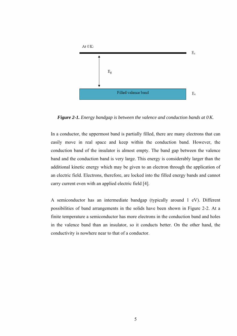
Eg= Ec- Ev , (2.1)
where Ec is the lowest energy of the conduction band and Ev is the highest energy of the
valence band.
5
Figure 2-1. Energy bandgap is between the valence and conduction bands at 0 K.
In a conductor, the uppermost band is partially filled, there are many electrons that can
easily move in real space and keep within the conduction band. However, the
conduction band of the insulator is almost empty. The band gap between the valence
band and the conduction band is very large. This energy is considerably larger than the
additional kinetic energy which may be given to an electron through the application of
an electric field. Electrons, therefore, are locked into the filled energy bands and cannot
carry current even with an applied electric field [4].
A semiconductor has an intermediate bandgap (typically around 1 eV). Different
possibilities of band arrangements in the solids have been shown in Figure 2-2. At a
finite temperature a semiconductor has more electrons in the conduction band and holes
in the valence band than an insulator, so it conducts better. On the other hand, the
conductivity is nowhere near to that of a conductor.

6
Figure 2-2. Schematic illustration of energy bands in (a) a conductor with two
possibilities (either the partially filled conduction band shown at the upper portion or
the overlapping bands shown at the lower portion), (b) a semiconductor, and (c) an
insulator [3].
In semiconductor materials, two kinds of bandgaps can be observed. One is a direct
band gap, another is an indirect band gap. Figure 2-3 (a) shows the band structure of a
semiconductor with a direct bandgap. In the case of the direct band gap, the maximum
of the valence band Ev is directly located below the minimum of the conduction band Ec
in the k-space (k is wave vector). In a direct band gap semiconductor, the electrons from
the conduction band minimum can combine directly with the holes at the valence band
maximum, while conserving the momentum. The energy of the recombination across
the bandgap is emitted in the form of a photon. Semiconductors such as GaAs, InP,
InGaAs, GaN etc. are examples of direct bandgap semiconductors [5]. Figure 2-3 (b)
shows the band structure of an indirect semiconductor. An indirect bandgap is a band
gap in which the energy minimum of the conduction band is shifted by a k-vector from
the valence band maximum. Since the different k-vectors represent the difference in
momentum, it makes the recombination of electrons to the valence band a second-order
process. That is why indirect bandgap materials, such as silicon carbide, are inefficient
at emitting light.

7
(a) (b)
Figure 2-3. Band structure of (a) a direct semiconductor and (b) an indirect
semiconductor [6].
2.3 Crystal structure
In a crystal, the atoms are arranged in a regulator pattern that repeats throughout the
material. The periodic arrangement of atoms in a crystal is called a lattice [3]. All the
lattice points are geometrically equivalent. A lattice therefore exhibits perfect
translational symmetry and, relative to an arbitrarily chosen origin, at a lattice point, any
other lattice point has the position vector [7]
r123 = n1a + n2b + n3c , (2.2)
where n is necessarily an integer and the vectors a, b and c are fundamental units of the
translational symmetry. There are fourteen different lattice structures which are called
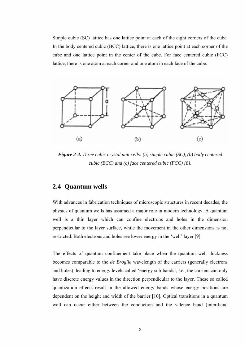
the Bravais lattices. Figure 2-4 shows the three most important cubic lattice structures.
8
Simple cubic (SC) lattice has one lattice point at each of the eight corners of the cube.
In the body centered cubic (BCC) lattice, there is one lattice point at each corner of the
cube and one lattice point in the center of the cube. For face centered cubic (FCC)
lattice, there is one atom at each corner and one atom in each face of the cube.
Figure 2-4. Three cubic crystal unit cells: (a) simple cubic (SC), (b) body centered
cubic (BCC) and (c) face centered cubic (FCC) [8].
2.4 Quantum wells
With advances in fabrication techniques of microscopic structures in recent decades, the
physics of quantum wells has assumed a major role in modern technology. A quantum
well is a thin layer which can confine electrons and holes in the dimension
perpendicular to the layer surface, while the movement in the other dimensions is not
restricted. Both electrons and holes see lower energy in the ‘well’ layer [9].
The effects of quantum confinement take place when the quantum well thickness
becomes comparable to the de Broglie wavelength of the carriers (generally electrons
and holes), leading to energy levels called ‘energy sub-bands’, i.e., the carriers can only
have discrete energy values in the direction perpendicular to the layer. These so called
quantization effects result in the allowed energy bands whose energy positions are
dependent on the height and width of the barrier [10]. Optical transitions in a quantum
well can occur either between the conduction and the valence band (inter-band

9
transition) or within the conduction band (inter-sub-band transition) as shown in Figure
2-5.
Figure 2-5. Optical inter-band and inter-sub band transitions in a quantum well.
Quantum wells can be fabricated by forming heterojunctions between different
semiconductors. From an electronic viewpoint, the semiconductors are different because
they have different band structures. Of course, there are many other properties which
are also different, such as dielectric constant, the lattice constant and the effective mass
[11]. Typically, the quantum wells are grown by epitaxy and usually a lattice mismatch
between the two different materials is produced.

10
3 Gallium Nitride
Recent years have shown the need for high-efficiency optoelectronic materials.
Therefore, research and development in optoelectronics technology has boomed. The
compound semiconductor materials offer the advantage of high luminous performance.
Especially, group III-N materials are particularly suitable for ultra violet, blue and green
light emitting devices. This chapter gives a basic overview of the crystalline structure
and the properties of GaN.
3.1 Crystal structure of GaN
GaN can have two lattice structures. It can be either hexagonal wurtzite (α-GaN) or
cubic zinc blende (β-GaN). The wurtzite structure is the most widely used form of GaN.
The crystal structure of the GaN layers used in this thesis is also the wurtzite. Therefore,
some of the properties of such a structure are described below.
Wurtzite structure of GaN is a symmetrical hexagonal structure and consists of
tetrahedrally coordinated gallium and nitrogen atoms that are stacked in an ABABAB…
pattern. Figure 3-1 shows the wurtzite structure of GaN, where c and a are two lattice
parameters, u is the dimensionless parameter which characterizes the bond aligned
along the main axis. The parameter u is measured in units of the c-axis lattice parameter,
and provides information about the distortion in the unit cell [12].

11
Figure 3-1. Hexagonal wurtzite structure of GaN [13].
There are two possibilities to deviate from the ideal wurtzite structure (c/a = 1.633 and
u = 0.375), i.e., by changing the c/a ratio or by changing the u value [14]. Such
deviations are often observed in wurtzite type structures [15] but there exists a strong
correlation between the c/a ratio and the u parameter. If the c/a decreases, then u
increases in such a way that the four tetrahedral distances remain nearly constant and
the tetrahedral angles are distorted [16]. The bond lengths would be equal if [14]
41
31
2
2
+×=cau . (3.1)
Table 3-1 shows the structural parameters of GaN, AlN and InN. For GaN, the wurtzite
structure is nearly ideal.

12
Lattice
Parameter GaN AlN InN
a 3.174 Å 3.091 Å 3.538 Å
c 5.169 Å 4.954 Å 5.707 Å
u 0.3786 Å 0.3815 Å 0.3792 Å
c/a 1.627 1.601 1.612
Table 3-1. Lattice parameters for common III-N compounds [17].
3.2 Energy band of GaN
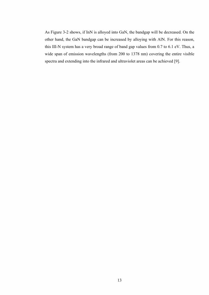
GaN is a direct band gap semiconductor material, and it has a band gap energy of about
3.48 eV. Figure 3-2 shows the bandgap energy of the three different III-nitride (III-N)
materials (AlN, GaN and InN) as a function of lattice constant.
Figure 3-2. Bandgap energy vs. lattice constant of InN, GaN and AlN [18].
13
As Figure 3-2 shows, if InN is alloyed into GaN, the bandgap will be decreased. On the
other hand, the GaN bandgap can be increased by alloying with AlN. For this reason,
this III-N system has a very broad range of band gap values from 0.7 to 6.1 eV. Thus, a
wide span of emission wavelengths (from 200 to 1378 nm) covering the entire visible
spectra and extending into the infrared and ultraviolet areas can be achieved [9].

14
4 Experimental Methods
This chapter discusses the experimental methods used in this thesis. Firstly, a brief
overview of the fabrication technique of the samples used for our research is presented.
The next section highlights the method used for the irradiation of quantum wells. The
last part of the chapter discusses the measurement techniques used in this work.
4.1 Metalorganic vapor phase epitaxy
There are several ways for fabricating epitaxial layers of III-nitrides such as liquid
phase epitaxy (LPE), molecular beam epitaxy (MBE), hydride vapor phase epitaxy
(HVPE) and metalorganic vapor phase epitaxy (MOVPE). In our study, all the samples
were fabricated by MOVPE, so only this method will be introduced.
Metalorganic vapor phase epitaxy (MOVPE) is a chemical vapor deposition method of
epitaxial growth, especially for compound semiconductors from organic compounds or
metalorganics and metal hydrides containing the required chemical elements.
The MOVPE process starts with a gas mixture which contains the molecular
compounds, termed precursors (necessary for growth), and a carrier gas. The latter is
usually hydrogen, with an operating pressure between 7.5 Torr and atmospheric
pressure (750 Torr). The chemical reactions take place inside a chamber which contains
a heated substrate. Close to this substrate, the precursors are ‘cracked’ (i.e.,

15
decomposed), which leads to a series of chemical reactions between the reactive species
created by the cracking process. The result of these reactions is the deposition of a thin
film on the substrate. The simplest case involves a pyrolysis reaction of vapors of a
volatile metalorganic (MO) compound and a gaseous hydride, given by [19]
nRHADDHAR nn +→+ , (4.1)
where R is an organic radical of some unspecified form but generally of low order, such
as methyl- or ethyl-radical, and A and D are the constituent species for the deposited
solid. There are a number of reactions of the group III and V source molecules as well
as growth related surface processes such as the adsorption or desorption of chemical
species and surface migration. A schematic overview of such processes is shown in
Figure 4-1. For reasons of uniform deposition low pressures are preferred. This is a
consequence of the more laminar flow pattern and the more homogeneous temperature
field within the reactor.
Figure 4-1. Schematic illustration of the basic processes of MOVPE.
16
The MOVPE growth process consists of many parallel and serial reaction steps
occurring simultaneously. For serial reactions, the slowest step controls the overall
reaction rate. For parallel reactions, the overall reaction rate is the sum of the individual
reaction rates, hence the fastest reaction controls the overall reaction rate [20].
In a MOVPE systems, the most important elementary steps determining the overall
reaction rate is controlled by an interplay between thermodynamics, kinetics and
hydrodynamics of the processes. The thermodynamics of growth describes the driving
force for the overall growth process by indicating in which direction the reactions will
proceed and predicting the solid stoichiometry [20]. Kinetics controls the rate at which
the possible gas phase and surface reactions occur [21]. The hydrodynamics of the
process controls the mass transport of the molecules in the gas phase, the temperature
distribution, the velocity profile and the total pressure in the reactor [20].
4.2 Radiation
Generally speaking, radiation is all around us. There are, however, different types of
radiation, some coming from natural sources and some which is created by humans. The
amount of radiation that semiconductor devices and materials encounter during their
lifecycle strongly depends on the radiation environments and their operating conditions.
For example, in space missions it is obvious that there is a radiation-harsh environment.
However, also during the fabrication process and even for standard terrestrial operation,
the devices may suffer from ionizing radiation [22].
4.2.1 Radiation effects on semiconductors
A semiconductor device in a radiation environment is generally subjected to a mix of
particles, with quite a range of energies. When an energetic particle travels through a
solid state system, it may lose its energy in various ways, thereby creating various types
of defects. In this section, the ionization and displacement damage will be introduced.

17
Ionization damage is the dominant mechanism when energetic particles interact with
solid-state matter. Ionization ability depends on the energy of the impinging individual
particles, and not on their number. A large flood of particles generally will not cause
ionization if these particles do not carry enough energy to be ionizing. The passage of
the ionizing radiation through matter can be effectively studied by considering both
electromagnetic radiation with photons from γ or x-rays and heavy and light charged
particles.
Semiconductor devices operated in a radiation environment such as in space must
exhibit the high-radiation hardness due to high-energy radiation. When a high-energy
particle traverses a semiconductor device, the energy transferred during an elastic or
inelastic nuclear collision maybe large enough to knock some atoms from their lattice
site. The knock-on atoms primarily create Frenkel defects which are pairs of point
defects close enough to exhibit an interaction: vacancy and an atom in an interstitial
position. For collisions hard enough to allow large energy transfer, the knock-on atoms
can collide with other atoms, creating more vacancies and interstitial atoms. When these
defects are closely space, a cluster of defects can be created. The presence of such
defects produce changes in the properties of the semiconductor [23].
Figure 4-2. Diagram of displacement damage [24].

18
In general, any disturbance of the lattice periodicity may give rise to energy levels in the
bandgap. The radiation induced defects have a major impact on the electrical and
optical behavior of semiconductor materials and devices [25].
4.2.2 Particle types
The constituent particles that compose of the radiation fields previously described can
be classified as either photons, neutrons or charged particles. Photons can be from γ or
x-rays, which are capable of interacting with the material via the photoelectric effect.
The neutron interaction is generated by elastic and inelastic scattering. And the charged
particles consist of electrons, protons, and light/heavy ions. They are able to interact via
Rutherford scattering or nuclear interactions depending on their mass [26].
4.2.3 Light and heavy ions
It is common knowledge that the charged particles can be distinguished by mass. Light
or heavy ions refer to an ionized atom which is usually lighter or heavier than helium.
Ion reactions are often used to produce intense neutron sources. The light ions are often
the projectiles of choice for this purpose. This is because in certain cases at least one
neutron may be quite loosely bound in the projectile, for example, the binding energy of
the deuteron is only 2.2 MeV, which could be compared with a value of 6 to 8 MeV for
heavy mass nuclei [27]. Both light-ion irradiation and heavy-ion irradiation produce
point defects, but the resultant defect morphology is quite different [28]. A light ion is
expected to create isolated point defects, whereas a heavy ion tends to yield clusters of
point defects [29, 30, 31, 32].

19
4.2.4 Radiation for LED materials
Modern LEDs are often based on III-V group materials with quantum well structures for
example the GaN/InGaN/GaN system is shown in Figure 4-3. There have been a few
studies conducted on the impact of radiation on GaN and its related alloys, most of
which have been performed on either GaAs or its related alloys. It has been shown that
irradiation changes the optical absorption, the refractive index, the photoluminescence,
and the photoconductivity of III-V materials. However, in the case of MQW structures
ion damage may be used beneficially to produce so-called quantum well intermixing
(QWI), which provides an elegant method for local bandgap engineering of a LED [22].
On the other hand, the non-radiative damage centers may be doubled, thus deteriorating
the properties of LED devices.
Figure 4-3. Schematic of the GaN/InGaN/GaN structure [33].
4.3 Measurement methods
To investigate the effect of radiation on the quantum wells, X-ray diffraction (XRD)
and photoluminescence (PL) studies have been performed on the samples.

20
4.3.1 X-ray diffraction
X-rays are invisible, but they travel in straight lines and affect a photographic film in
the same way as ordinary visible light. In 1912, X-ray diffraction (XRD) by crystals
was discovered, and this discovery simultaneously proved the wave nature of X-rays
and provided a new method for investigating the fine structure of matter [34]. In XRD,
X-rays are reflected from adjacent crystal planes separated by a distance when the path
difference between them is an integer multiple of the wavelength used. This condition is
known as the Bragg’s law
λθ nd =sin2 , (4.2)
where d is the distance between the two neighboring lattice planes, θ is the Bragg angle,
n is an integral number which describes the order of reflection and λ is the wavelength
of the X-rays.
In this work a high-resolution X-ray diffraction (HR-XRD) system was used. The
system is a Philips X’Pert Pro diffractometer, which can be operated in three axis
configuration. Figure 4-4 shows the schematic illustration of the XRD setup. In this
setup an analyzer crystal is located in front of the detector in the diffracted beam path to
improve the angular resolution. A four crystal germanium monochromator is used to
select the 1αKCu − line (λ =1.541 Å) from the emission spectrum of the X-ray tube
[35]. An X-ray mirror is placed in front of the monochromator that is used to reduce the
divergence of the incident beam.

21
Figure 4-4. Schematic illustration of the high-resolution X-ray diffraction setup.
The compositional analysis can be done by using the rocking curve scans. In a rocking
curve scan the sample is moved over a very small angular range. The graphs can be
intensity vs. ω or intensity vs. θω 2− . The XRD curve obtained from the samples was
analyzed by a simulation software to achieve the thickness of the barrier layer and the
individual composition of the different elements in quantum wells layers.
4.3.2 Photoluminescence
Photoluminescence (PL) spectroscopy provides one of the most useful methods to
investigate the optical quality of heterostructures [36]. The PL spectra provide the
transition energies, which can be used to identify the electronic energy levels. In a
quantum mechanical field, a PL process can be described as an excitation of carriers to
a higher energy state and then a return to a lower energy state resulting in photon
emission. PL is a simple, versatile, and non-destructive technique, however, the
fundamental limitation of PL analysis is its dependence on radiative events. Materials
with poor radiative efficiency are difficult to study via common PL.

22
When continuous wave (CW) excitation is used in a PL experiment, the system quickly
converges to the steady state. The rate of excitation is the same as the rate of
recombination, and the photo-generated carrier density is constant in time. In contrast,
when the excitation is caused by a series of short laser pulses, the density of carriers
depends on time. The laser pulse can be much shorter than the recombination time, so a
specific carrier concentration can be generated almost instantaneously. For this reason,
time-resolved photoluminescence (TR-PL) can be helpful in determining carrier
lifetimes and to identify and characterize various recombination mechanisms in the
material [37].
The setup of continuous wave PL is very simple, including an optical source (pump
laser), a spectrophotometer and an optical fiber. Figure 4-5 shows the schematic of the
CW-PL setup used in this thesis. A He-Cd laser with a maximum power of 0.02 W at
325 nm was used as the excitation source. A set of mirrors and lenses was used to align
and focus the laser beam onto the samples. The PL coming out of the sample was
collected and fed to a spectrometer via an optical fiber.
Figure 4-5. Diagram of the basic CW-PL setup used in this work.
In addition, the PL intensity at different temperatures can be used to further characterize
the underlying electronic states and energy bands in the material [38]. At the lowest
temperature, the radiative recombination is a dominant phenomenon. With increasing
temperature the radiative recombination decreases. In contrast, the non-radiative
recombination processes tend to increase with the rising temperature. Based on the
23
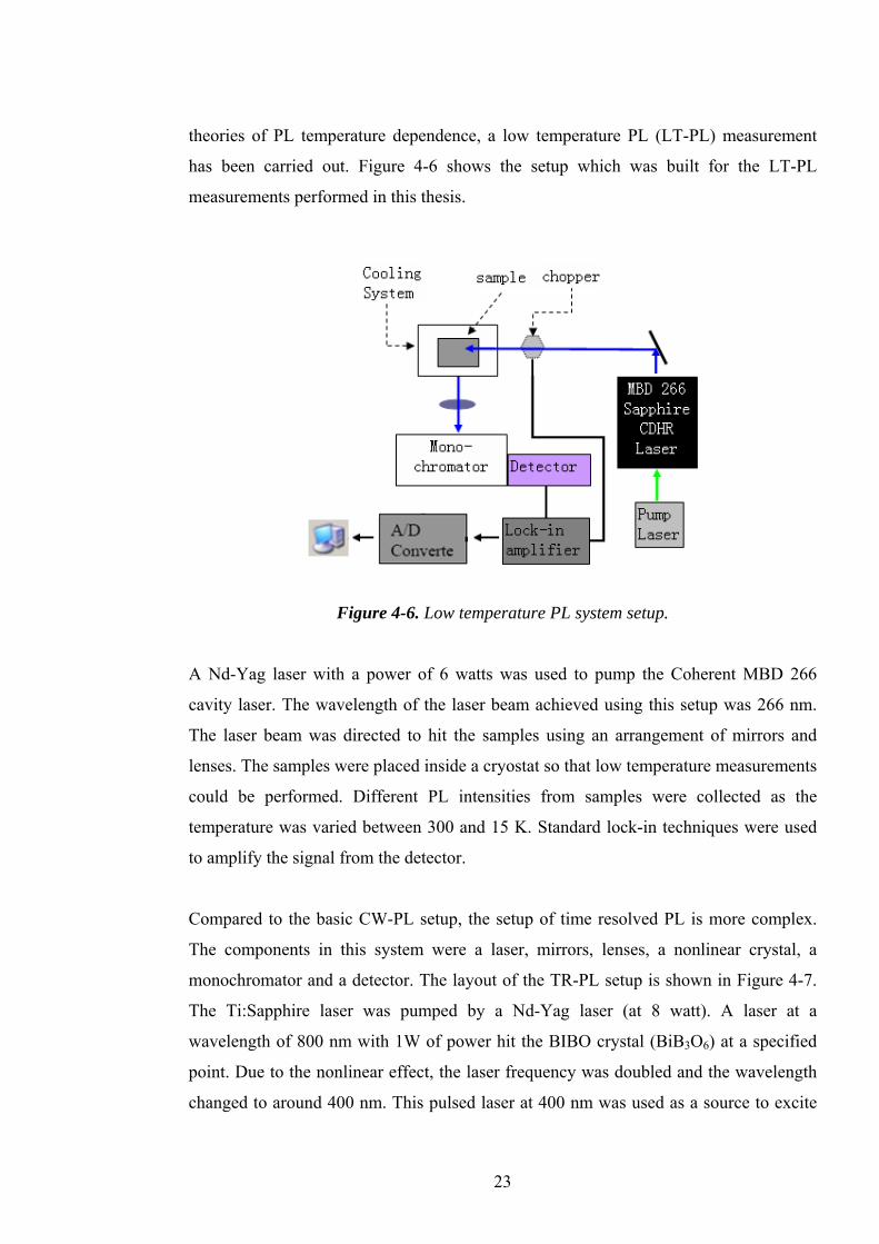
theories of PL temperature dependence, a low temperature PL (LT-PL) measurement
has been carried out. Figure 4-6 shows the setup which was built for the LT-PL
measurements performed in this thesis.
Figure 4-6. Low temperature PL system setup.
A Nd-Yag laser with a power of 6 watts was used to pump the Coherent MBD 266
cavity laser. The wavelength of the laser beam achieved using this setup was 266 nm.
The laser beam was directed to hit the samples using an arrangement of mirrors and
lenses. The samples were placed inside a cryostat so that low temperature measurements
could be performed. Different PL intensities from samples were collected as the
temperature was varied between 300 and 15 K. Standard lock-in techniques were used
to amplify the signal from the detector.
Compared to the basic CW-PL setup, the setup of time resolved PL is more complex.
The components in this system were a laser, mirrors, lenses, a nonlinear crystal, a
monochromator and a detector. The layout of the TR-PL setup is shown in Figure 4-7.
The Ti:Sapphire laser was pumped by a Nd-Yag laser (at 8 watt). A laser at a
wavelength of 800 nm with 1W of power hit the BIBO crystal (BiB3O6) at a specified
point. Due to the nonlinear effect, the laser frequency was doubled and the wavelength
changed to around 400 nm. This pulsed laser at 400 nm was used as a source to excite

24
the InGaN/GaN quantum wells emitting at 460 nm. The emitted photons were collected
by the detector and photon-counting electronics was used to create the time-resolved
curve.
Figure 4-7. Diagram of the TR-PL setup used in this work.

25
5 Results and Discussion
Section 5.1 of this chapter explains the growth conditions of the samples used in this
study. Section 5.2 discusses the irradiation by heavy ions. The later sections of the
chapter highlight the results that have been achieved from the XRD and PL
measurements of the samples.
5.1 Growth of InGaN/GaN multiple quantum wells
For this study, multiple quantum well (MQW) structures were grown on 430 μm thick
c-plane sapphire substrates by metal organic vapor phase epitaxy (MOVPE). Ammonia
(NH3), trimethylindium (TMIn), and trimethylgallium (TMGa) were used as the N, In
and Ga source, respectively.
All the samples used in this study consist of a 3 μm thick undoped GaN buffer layer
between the substrate and the MQW structure. The famous two-step method has been
used in GaN buffer layer growth. This method reduces the amount of dislocations in the
buffer layer [39].
Two different series of MQW structures were grown. The series A consisted of 5
quantum wells in the MQW structure and an indium composition of 6% in the active
region of the wells. In the series B include the samples have 10 QWs in the MQW
structure and the indium composition is around 10%. The main sample properties are

26
listed in Table 5-1. The temperature during the growth of the active region has been
used primarily to control the amount of indium in the wells.
Samples Number of Wells Temperature In composition (%)
Series A 5 790℃ 6%
Series B 10 750℃ 10%
Table 5-1. Some properties of the sample series.
GaN has been used as a barrier layer with a thickness of 25 nm in all samples. The
thickness of the InGaN layers is around 3nm for all the samples. Figure 5-1 shows the
simplified form of heterostructures used in this research.
Figure 5-1. Schematic illustration of the sample structure in a) series A having 5 QWs
with 6% indium and b) series B having 10 QWs with 10% indium. The MQW structures
of all the samples are covered only by the topmost GaN barrier.

27
5.2 Irradiation by heavy ions
The samples were irradiated with heavy ions having energies below 1MeV/u (mega-
electron volt/atomic mass unit) delivered from the 5 MV tandem accelerator based in
Uppsala. These irradiations were performed at room temperature under normal
incidence with respect to the sample surface. The applied ion fluences were in the range
of 109 to 1012 ions/cm2, and homogeneous irradiation over an area of 30x30 mm2 was
achieved by means of an electrostatic raster scanner. The ion fluence was determined
from the irradiation time and the beam current, which was measured using a Faraday
cup with 1.0 cm2 aperture located behind the sample holder. The energies and ion types
used in this study were 13 MeV Br3+ and 40MeV I9+ ions. Computer simulations
indicate that both kinds of projectiles completely penetrate the layers of the MQWs in
the used samples. The penetration depths in GaN are 3.4 and 6.1 μm for the used Br and
I ions, respectively. Table 5-2 summarizes the sample details and the heavy ion fluences
used in the experiments.
Series Sample structure and composition Heavy ions and fluence ranges
A 5 QWs
6% Indium in wells
40 MeV I
1.5x10⁹ - 6x10¹² ions/cm2
13 MeV Br
5.6x10⁹ - 1.1x10¹¹ ions/cm2
B 10 QWs
10% Indium in wells
40 MeV I
1.5x10⁹ - 6x10¹² ions/cm2
13 MeV Br
5.6x10⁹ - 1.1x10¹¹ ions/cm2
Table 5-2. MQW samples, the bombardment ions and the fluence ranges used in this
study.

28
5.3 XRD results
It has been described is section 4.3.1 that XRD is a powerful tool in determining the
quality of the crystal structure of a quantum wells. The θω 2− XRD scans have been
used to analyze the crystal structure of our samples with and without irradiation. Figure
5-2 shows the θω 2− scan of a 5 QW sample without any irradiation.
Figure 5-2. The θω 2− curves of the 5 QW sample (Ref2) without any irradiation.
The sharpest peak in Figure 5-2 comes from the GaN buffer layer. A diffraction peak
from the MQW stack can be seen on the left of the GaN peak. Apart from this, there are
several sharp satellite peaks that are visible in this curve. The sharpness of these peaks
is indicative of the fact that the quality of the interface between individual layers of the
structure under investigation is fairly good.
To investigate the effect of the different fluences of either the I9+ or Br3+ ions, XRD
scans were performed on various samples. Figure 5-3 shows the θω 2− curves of the 5
QW samples with ion fluences ranging between 5.3x10⁹ and 6.0x10¹² ions/cm2. The 5
QW reference sample (Ref2) without any irradiation has also been included for easy
comparison.

29
Figure 5-3. θω 2− curves of the samples which were selected from Series A (5 QWs
structure) with different I9+ fluencies.
The comparison of XRD scans (Figure 5-3) with various fluences of I9+ ions reveals that
there has been no major damage to the crystal structure of the MQWs. We have
concluded this from the fact that there is no visible change either in the periodicity or
the full width half maximum (FWHM) of the diffraction and satellite peaks. This
indicates that despite high doses of I9+ ions, the crystal structure is intact and the
interface quality is still the same as in the sample not exposed to the irradiation.
Similar XRD measurements were performed on the 10 QW samples irradiated with I9+
and Br3+ ions. The θω 2− scans of those samples do not differ from that of the reference
sample and therefore, no major damage to the crystal structure was observed. It is
believed that there might be formation of some point defects (vacancy or interstitial) or
small clusters as a result of irradiation. Our XRD results have revealed that it is
extremely difficult to observe such defects with θω 2− scans.

30
5.4 Continuous wave photoluminescence results
The results obtained from the continuous wave photoluminescence (CW-PL)
measurements have been explained below. The measurement results have been
categorized according to the irradiation ions in the samples.
5.4.1 CW-PL results of samples irradiated by I9+ ions
This section covers the CW-PL results which are obtained from the samples irradiated
by 40 MeV I9+ ions with fluences in the range of 1.5x10⁹ - 6x10¹² ions/cm2. Figure 5-4
shows the room temperature PL spectra of the 5 QW samples irradiated with various
fluences of I9+ ions. The optical quality of the samples degrades with increasing ion
fluence. A fluence of 1.5x10⁹ ions/cm2 reduces the PL intensity by 30%. When the ion
fluence is larger than 5.0x10¹⁰ ions/cm2, the PL intensity is below the background noise
level, so the room temperature PL data for such samples has not been included in Figure
5-4.
Figure 5-5 shows the PL spectra of 10 QW samples irradiated with 40 MeV I9+ ions. It
is clearly evident from the CW-PL spectra that the I9+ ions greatly decrease the PL
intensity of the samples. A fluence of 1.5x10⁹ ions/cm2 reduces the PL intensity by 80%.
Increasing the I9+ ions fluence still decreases the optical quality of the samples. The
samples with the ion fluence of 5.0x10⁹ ions/cm2 or more severely damage the quantum
well structure optically. As a result, the PL intensity remains again below the
background noise level.

31
Figure 5-4. PL spectra of the 5 QW samples with different fluences of I9+ irradiation.
Figure 5-5. PL spectra of the 10 QW samples with different fluences of I9+ irradiation.

32
Figure 5-6 shows, the total integrated area under the PL peak as a function of the
fluence of 40MeV I9+ ions. The results indicate that the PL intensities from both the 5
and 10 QW structures have a strong dependence on the fluence of iodine ions. The
integrated room temperature PL intensity shows that there is a sharper degradation for
the 10 QW samples as compared to the 5 QW samples. We believe that the sharp drop
of the PL signal in the 10 QW samples as compared to the 5 QW samples could be that
an increased amount of indium content in the 10 QW samples causes much more strain
in the structure. These strained layers are much easier damaged by irradiation.
Figure 5-6. Total integrated PL intensity of 5 and 10 QW samples vs. the fluence of 40
MeV I9+ ions varying from 1.5x10⁹ to 1.0x10¹⁰ ions/cm2. The PL intensity of both the
curves has been normalized to one at zero fluence.

33
5.4.2 CW-PL results of samples irradiated by Br3+ ions
The CW-PL results shown in this section have been obtained from the 5 QW and 10
QW samples with 13MeV Br3+ ion irradiation. The fluence of Br3+ ions ranges from
1.5x10⁹ to 6x10¹² ions/cm2. Figure 5-7 shows the room temperature PL spectra of the 5
QW samples irradiated with various fluences of Br3+ ions. The optical quality of the
samples degrades as the Br3+ ion fluence increases.
Figure 5-7. PL spectra of the 5 QW samples with different fluences of Br3+ irradiation.
Figure 5-8 shows the room temperature CW-PL spectra of 10 QW samples with 13MeV
Br3+ ion irradiation. It is clearly evident from the PL spectra that the PL intensity
decreases with increasing ion fluence.
Figure 5-9 shows the total integrated PL intensity as a function of the fluence of 13
MeV Br3+ ions. The results are similar to the samples irradiated with 40 MeV I9+ ions.
The PL intensities from both the 5 and 10 QW structures strongly depend on the fluence
of the Br3+ ions. Here again we see that the optical damage caused by the Br3+ ions in
the 10 QW samples is more severe than in 5 QW samples. It is also noticeable that the
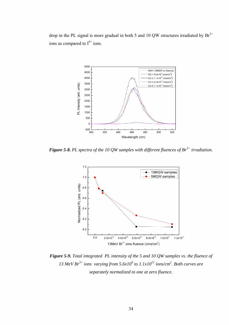
34
drop in the PL signal is more gradual in both 5 and 10 QW structures irradiated by Br3+
ions as compared to I9+ ions.
Figure 5-8. PL spectra of the 10 QW samples with different fluences of Br3+ irradiation.
Figure 5-9. Total integrated PL intensity of the 5 and 10 QW samples vs. the fluence of
13 MeV Br3+ ions varying from 5.6x10⁹ to 1.1x10¹¹ ions/cm2. Both curves are
separately normalized to one at zero fluence.

35
5.5 Low temperature photoluminescence results
To further extend our investigation, temperature dependent PL measurements were
carried out. As we know, the PL intensity gives us information about the radiative and
non-radiative recombination rates. A variation of external parameters such as
temperature can be used to further characterize the underlying electronic states and
energy bands in the material [40]. In this section, we have investigated the effect of
radiation on the activation energy and the internal quantum efficiency of the samples.
5.5.1 Activation energy
In our low temperature PL measurement results, the logarithm of the PL intensity vs.
the reciprocal of the temperature has been used to study the effect of temperature
variation on quantum wells. These graphs often referred to as Arrhenius plots, have
been used in previous quantum well studies [41]. Figure 5-10 shows integrated PL
intensities irradiated with various fluences of 40 MeV I9+ ions. The temperature range
used for these experiments is between 15 K and 293 K. It clearly indicates that as the
temperature is increasing, the normalized PL intensities of all the samples are reduced.
To further characterize the temperature dependent curves shown in Figure 5-10, we use
the commonly known Arrhenius equation
.....)/exp()/exp(1)(
2211
0
+−+−+=
TETEI
TIBaBa κακα
, (5.1) [42]
where I(T) is the integrated PL intensity at temperature T, T is the temperature, Bκ is
Boltzmann constant, iα is a constant expressing the recombination probability of
process i, iaE is the activation energy of process i and I0 is the PL intensity at lowest
temperature. Form the basic principle of activation energy, if the PL measurement
temperature is very low (close to 0 K), the electrons and holes that are generated by
external light pumping cannot escape from the quantum well. Thus, all the generated
electrons and holes recombine in the quantum structures, and the integrated PL intensity

36
(I0 which is shown in Eq.5.1) is larger than the one measured at any other temperature.
As we move towards higher temperatures, carriers in the quantum structures are
affected by the thermal activation energy, and they start to escape from the wells, and
the PL intensity drops [43]. The estimated activation energies of the InGaN/GaN 5 QW
and 10 QW samples with different fluences of I9+ ions are shown in Table 5-3.
Figure 5-10. Arrhenius plots of integrated PL intensities for InGaN/GaN QW samples
with a) 5 QWs and b) 10 QWs as a function of the fluence of I9+ ion irradiation. All
the curves are separately normalized to one at the lowest temperature.

37
Samples (5 QWs)
Estimated
activation
energies (meV)Samples
(10 QWs)
Estimated
activation
energies (meV)
Ea1 Ea2 Ea1 Ea2
Ref2 (no fluence) 30.5 104.0 Ref1 (no fluence) 32.1 102.0
G3-1(1.5x10⁹ ions/cm2) 28.9 89.0 G1-1(1.5x10⁹ ions/cm2) 31.4 86.2
G3-2(5.3x10⁹ ions/cm2) 26.5 73.3 G1-2(5.3x10⁹ ions/cm2) 29.9 76.0
G3-3(1.0x10¹⁰ ions/cm2) 24.4 66.1 G1-3(1.0x10¹⁰ ions/cm2) 22.9 60.1
G3-4(5.0x10¹⁰ ions/cm2) 22.6 57.5 G1-4(5.0x10¹⁰ ions/cm2) 20.6 49.1
G3-5(1.0x10¹¹ ions/cm2) 17.3 50.6 G1-5(1.0x10¹¹ ions/cm2) 17.6 39.2
Table 5-3. Estimated activation energies in the 5 QW and 10 QW samples with different
I9+ ion fluences.
Table 5-3 clearly shows that the energy levels seen in Ref 1 and Ref 2 samples are the
same. We believe that in the irradiated samples there are more than 2 levels as the
activation energy is changing continuously. It means that the irradiation is creating
shallow levels. These shallow levels are not related to yellow luminescence, which
originates from deeper levels.
The integrated PL intensities of the 5 and 10 QW samples irradiated with 13 MeV Br3+
ion and the estimated activation energies are shown in Figure 5-11 and Table 5-4,
respectively.
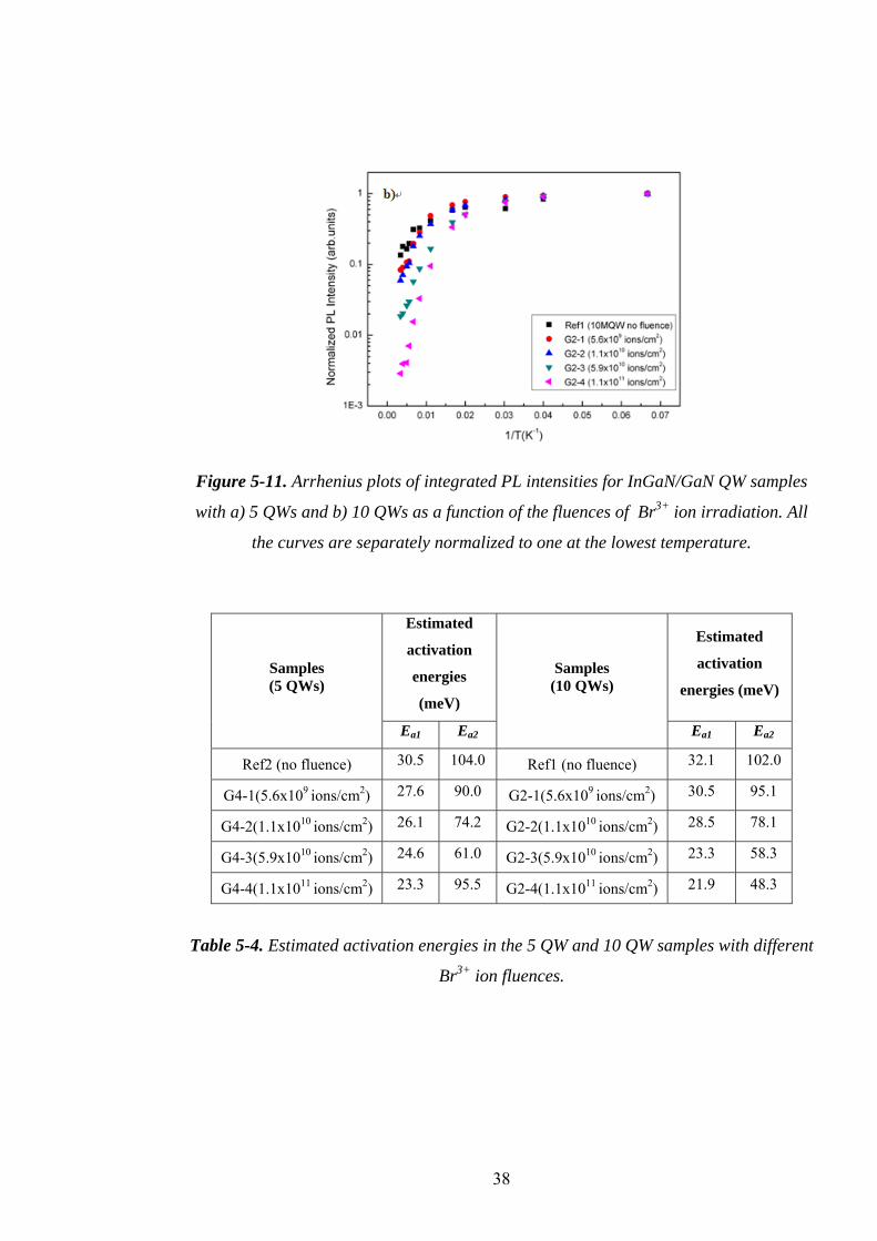
38
Figure 5-11. Arrhenius plots of integrated PL intensities for InGaN/GaN QW samples
with a) 5 QWs and b) 10 QWs as a function of the fluences of Br3+ ion irradiation. All
the curves are separately normalized to one at the lowest temperature.
Samples (5 QWs)
Estimated
activation
energies
(meV)
Samples (10 QWs)
Estimated
activation
energies (meV)
Ea1 Ea2 Ea1 Ea2
Ref2 (no fluence) 30.5 104.0 Ref1 (no fluence) 32.1 102.0
G4-1(5.6x10⁹ ions/cm2) 27.6 90.0 G2-1(5.6x10⁹ ions/cm2) 30.5 95.1
G4-2(1.1x10¹⁰ ions/cm2) 26.1 74.2 G2-2(1.1x10¹⁰ ions/cm2) 28.5 78.1
G4-3(5.9x10¹⁰ ions/cm2) 24.6 61.0 G2-3(5.9x10¹⁰ ions/cm2) 23.3 58.3
G4-4(1.1x10¹¹ ions/cm2) 23.3 95.5 G2-4(1.1x10¹¹ ions/cm2) 21.9 48.3
Table 5-4. Estimated activation energies in the 5 QW and 10 QW samples with different
Br3+ ion fluences.

39
5.5.2 Internal quantum efficiency
The temperature dependent photoluminescence (PL) was used to determine the internal
quantum efficiency (IQE) of the QW structures. At very low temperatures the non-
radiative recombination is close to minimum and radiative recombination processes are
dominant. With increasing temperature, non-radiative recombination processes get
activated and play a key role at room temperature [44]. Figure 5-12 shows the IQE of
samples with different irradiation fluencies calculated from
K
K
PLPLIQE
15
300= , (5.2)
where PL300K is the PL intensity at room temperature and PL15k is the PL intensity at the
lowest temperature in our system.
The IQE of the samples irradiated with 40 MeV I9+ ions declines severely, which is
shown in Figure 5-12 a). From Figure 5-12 b), we find that the decrease of the IQE in
the samples irradiated with Br3+ ions is not as sharp as that in samples irradiated with I9+
ions. The possible reason can be the different nature of the Br3+ ions as compared to I9+.
As was mentioned in section 4.2.3, the Br3+ ions may create isolated point defects and
I9+ ions result small clusters of point defects or just large concentration of isolated point
defects. That is why the damage done to the samples are different in the case of
different ions.

40
Figure 5-12. Internal quantum efficiency of a) 5 QW and 10 QW samples irradiated by
40MeV I9+ ions and b) 5 QW and 10 QW samples irradiated by 13MeV Br9+ ions as a
function of irradiation fluence.
41
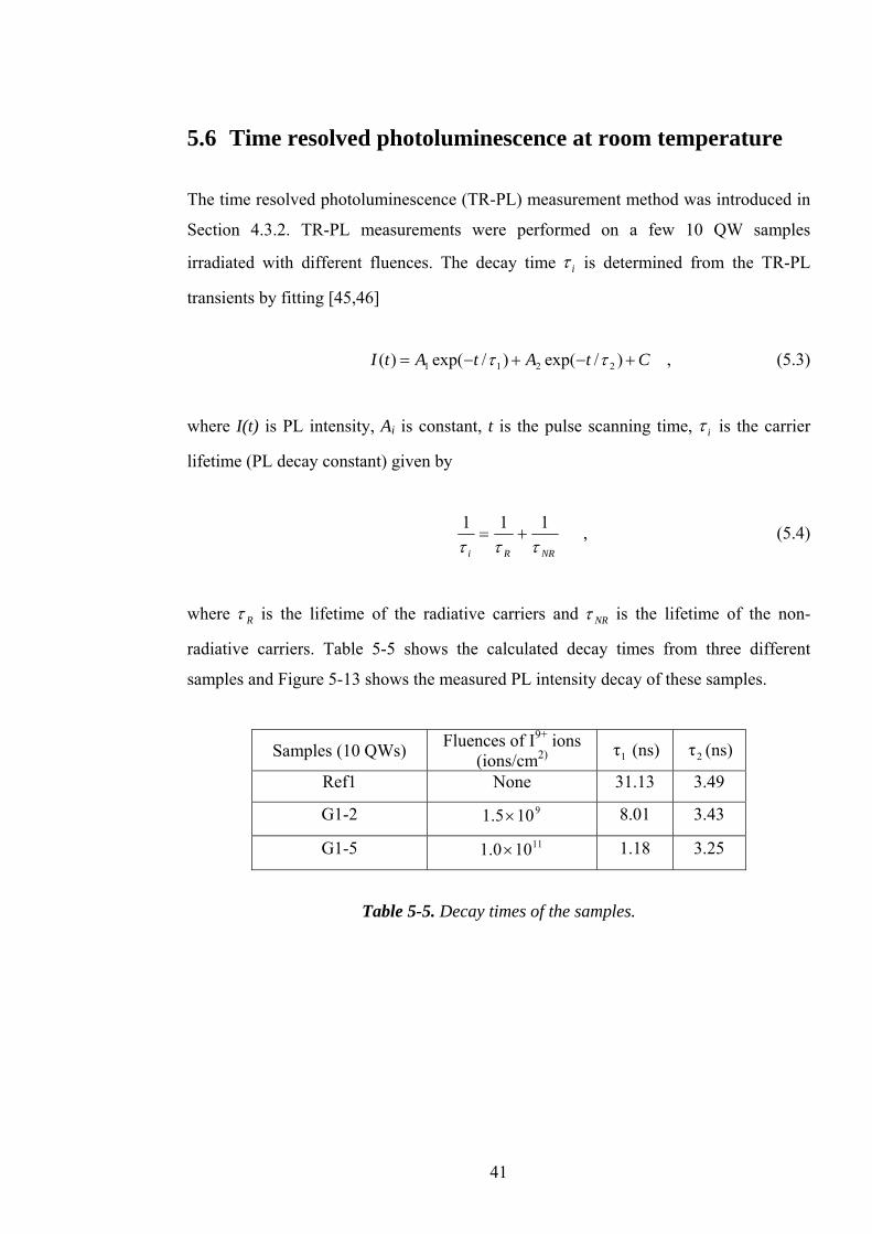
5.6 Time resolved photoluminescence at room temperature
The time resolved photoluminescence (TR-PL) measurement method was introduced in
Section 4.3.2. TR-PL measurements were performed on a few 10 QW samples
irradiated with different fluences. The decay time iτ is determined from the TR-PL
transients by fitting [45,46]
CtAtAtI +−+−= )/exp()/exp()( 2211 ττ , (5.3)
where I(t) is PL intensity, Ai is constant, t is the pulse scanning time, iτ is the carrier
lifetime (PL decay constant) given by
NRRi τττ111
+= , (5.4)
where Rτ is the lifetime of the radiative carriers and NRτ is the lifetime of the non-
radiative carriers. Table 5-5 shows the calculated decay times from three different
samples and Figure 5-13 shows the measured PL intensity decay of these samples.
Samples (10 QWs) Fluences of I9+ ions (ions/cm2) 1τ (ns) 2τ (ns)
Ref1 None 31.13 3.49
G1-2 9105.1 × 8.01 3.43
G1-5 11100.1 × 1.18 3.25
Table 5-5. Decay times of the samples.

42
Figure 5-13. Time dependent PL intensity of the samples with different fluences of I9+
ion irradiation.
It can be clearly seen that the decay time 1τ has notably decreased with the increase of
I9+ fluence, while 2τ is almost unchanged. The reason for the decrease in the decay time
with the increase of ion fluence could be the formation of localized point defects which
act as non-radiative recombination centers. The unchanged value of 2τ indicates that it
is related to a process not affected by irradiation. Because the time constant 2τ is so
large, the process can be related to spatial carrier separation by, e.g., the polarization
field.

43
6 Summary
The properties of irradiated InGaN/GaN multiple quantum wells have been studied by
XRD and PL techniques. MQW structures with different indium compositions and
different number of QWs were grown by MOVPE. The irradiation of quantum wells
was performed at room temperature with two different heavy ions (Br3+ and I9+). The
fluences of these ions were varied from 109 to 1012 ions/cm2.
The XRD rocking curves indicated that there has been no major damage to the overall
crystal structure of the quantum well samples. Even the samples with a very high
fluence of ions give no change in the FWHM or periodicity of the diffraction and
satellite peaks. We believe that the extent of the damage is very small and it is not
possible to observe the damage by XRD.
The PL measurements show that the optical properties of the samples irradiated with
both ions have a strong dependence on the fluences of heavy ions. The continuous wave
photoluminescence results at room temperature indicate that there is a sharp degradation
for samples irradiated with I9+ ions with increasing fluence. It is also noticeable that the
drop in the PL signal is more gradual in samples irradiated with Br3+ ions as compared
to I9+ ions. This phenomenon can be caused by the fact that bromine ion is lighter than
iodine ion. Also the energy of the bromine ion is lower than that of the iodine ion.
The low temperature PL measurement results clearly indicate that as the temperature is
increasing, the PL intensities of all the samples are reduced. The activation energy and

44
internal quantum efficiency of the samples also show a similar dependence on the
fluence of irradiation.
Due to the pump laser wavelength (around 400 nm), only 10 QW samples have been
studied in the time resolved PL measurement. The results show that the decay time
decreased significantly with the increase of heavy ion fluence. From the results of all
three types of PL measurements that were performed in the course of this research work,
it is believed that localized defects were created as a result of irradiation. The defects
could be point defects, Frenkel pairs, or small clusters of such defects.
For future work, transmission electron microscopy (TEM) should be used to study the
exact nature of the defects. High resolution TEM images can reveal the type and extent
of the damage caused in the quantum wells.

45
Appendix 1 Catalog of measured InGaN/GaN samples
Sample
name Description Fluence
Ref1 10 QWs, without irradiation no fluence
Ref2 5 QWs, without irradiation no fluence
G1-1
10 QWs, irradiated by 40MeV I9+
9105.1 × ions/cm2
G1-2 9103.5 × ions/cm2
G1-3 10100.1 × ions/cm2
G1-4 10100.5 × ions/cm2
G1-5 11100.1 × ions/cm2
G1-6 12101.1 × ions/cm2
G1-7 12100.6 × ions/cm2
G2-1
10 QWs, irradiated by 13MeV Br3+
9106.5 × ions/cm2
G2-2 10101.1 × ions/cm2
G2-3 10109.5 × ions/cm2
G2-4 11101.1 × ions/cm2
G3-1
5 QWs, irradiated by 40MeV I9+
9105.1 × ions/cm2
G3-2 9103.5 × ions/cm2
G3-3 10100.1 × ions/cm2
G3-4 10100.5 × ions/cm2
G3-5 11100.1 × ions/cm2
G3-6 12101.1 × ions/cm2
G3-7 12100.6 × ions/cm2
G4-1
5 QWs, irradiated by 13MeV Br3+
9106.5 × ions/cm2
G4-2 10101.1 × ions/cm2
G4-3 10109.5 × ions/cm2
G4-4 11101.1 × ions/cm2

46
Appendix 2 Fitting curves for the determination of activation energies Figure A and B show the curves obtained by fitting the data points with Arrhenius
Formula
.....)/exp()/exp(1)(
2211
0
+−+−+=
TETEI
TIBaBa κακα
,
Where I(T) is the integrated PL intensity at temperature T, T is the temperature, kB is
Boltzmann constant, Ea is equal to the activation energy and I0 is the PL intensity at
lowest temperature.
Figure A. Fitting curves for the samples irradiated with 13MeV Br3+ ions.
Figure B. Fitting curves for the samples irradiated with 40MeV I9+ ions

47
References [1] J. Grant, R. Bate, W. Cunninghama, GaN UV detectors for protein studies, Nuclear
Instruments and Methods in Physics Research A 563 (2006) 27–30.
[2] R.A. Smith, Semiconductor, 2nd ed., Cambridge Univ. Press, London, 1979.
[3] S.M. Sze, Semiconductor Devices Physics and Technology, 2nd ed., Wiley, New
York, 2001.
[4] M. Mansfield, C. O’Sullivan, Understanding Physics, Wiley, New York, 1998.
[5] J. Singh, Semiconductor Optoelectronics Physics and Technology, McGraw-Hill
International Editions, 1995.
[6] http://micro.magnet.fsu.edu/primer/lightandcolor/ledsintro.html
[7] H.P. Myers, Introductor Solid Sate Physics, Taylor and Francis London, 2nd edition,
1997.
[8] P. Kuivalainen, Physical Modeling of Semiconductor Devices, TKK, Espoo, 2006.
[9] M. Ali, MOVPE Growth of InAlGaN Layers and Quantum Structures for UV
Applications, Master thesis, TKK, Espoo, 2007.
[10] http://photon.soe.ucsc.edu/intersubband.html
[11] P. Harrison, Quantum Wells, Wires and Dots, Wiley, New York, 2000.
[12] T. Böttcher, Hetero-epitaxy of group III nitrides for the applications in laser diodes,
dissertation, University of Bremen, 2002.
[13] S. Muraleedharan, Processing of Gallium Nitride Blue Light Emitting Diode Chips,
Master thesis, TKK, Espoo, 2007.
[14] J. H. Edger , Properties, Processing and Applications of Gallium Nitride and
Related Semiconductors, INSPEC, London, 1999
[15] R. W. G Wyckoff, Crystal Structures vol. 1, Wiley, New York, 1965.
[16] H. Schulz, K.H. Thiemann, Solid State Commun. (USA) vol.23 (1977) p.815
[17] S. Nakamura, G. Fasol, The blue laser diode, Springer Verlag, Berlin, 1997.
[18] http://www.emf.co.uk/
[19] J.J. Coleman, Proceedings of IEEE. 85, 1715-1729, 1997.
[20] R. Steins, New Process Approaches to Metalorganic Vapor Phase Epitaxy of III-
nitrides for High Power HEMTs, Dissertation, 2006.

48
[21] M. A. Herman, W. Richter and H. Sitter, Epitaxy, Physical Principles and
Technical Implementation, Springer- Verlag, 2004.
[22] C.Claeys, E. Simoen, Radiation Effects in Advanced Semiconductor Materials and
Devices, Springer, 2002
[23] C. Leroy, P.G. Rancoita, Particle Interaction and Displacement Damage in Silicon
Devices Operated in Radiation Environment, Rep. Prog. Phys.70 (493-625) 2007.
[24] M. J. Beck, R. Hatcher, L Tsetseris, M Caussanel, Elemental Defect Processes in
Radiation Induced Displacement Damge in Si, 2006 MURI Review, 2006.
[25] J. R. Srour, c, IEEE transactions on nuclear science, Vol. 50, No. 3, 2003.
[26] A. K. Sutton, Displacement Damage and Ionization Effects Advanced Silicon-
Germanium Heterojunction Bipolar Transistors.
[27] Radiation Protection for Particle Accelerator Facilities, NCRP, (Report No. 144),
2003.
[28] V. D .S. Dhaka, N. V Tkachenko, H. Lemmetyinen, Effects of heavy-ion and light-
ion irradiation on the room temperature carrier dynamics of InGaAs/GaAs quantum
wells, Semicond. Sci. Technol. 21 (2006) 661-664.
[29] L. Joulaud, J. Mangeney, Thermal stability of ion-irradiated InGaAs with (sub-)
picoseconds carrier lifetime, Appl. Phys. Lett. 2003.
[30] J. Mangeney, J. Lopez , N. Stelmakh , J. M. Lourtioz, J.L. Oudar , H. Bernas,
Subgap optical absorption and recombination center efficiency in bulk GaAs irradiated
by light or heavy ions, Appl. Phys. Lett. 76, 40 (2000).
[31] J. Mageney, H. Choumane, G. Patriarche, G. Leroux, G. Aubin, J.C. Harmand, J. L.
Oudar, H. Bernas, Comparison of light- and heavy-ion-irradiated quantum-wells for use
as ultrafast saturable absorbers, Appl. Phys. Lett. 79, 2722 (2001).
[32] K. Nordlund, J. Peltola, J. Nord, J. Keinonen, and R. S. Averback, Defect
clustering during ion irradiation of GaAs: a molecular dynamics study, J. Appl. Phys. 90,
1710 (2001)
[33] N. A. Sanford, A. Munkholm, M. R. Krames, Refractive index and birefringence
of InxGa1–xN films grown by MOCVD, phys. stat. sol. (c) 2, No. 7, 2783–2786 , 2005
[34] B.D. Cullity, S.R. Stock, Elements of X-ray Diffraction (3th ed), Prentice Hall,
2001.

49
[35] S. Suihkonen, Fabrication of InGaN Quantum Wells for LED Application,
Doctoral Dissertation, Espoo, 2008.
[36] A.Y. Cho, Molecular Beam Epitaxy, AIP Press, New Jersy, 1994.
[37] T.H. Gfroerer, Photoluminescence in Analysis of Surfaces and Interfaces, John
Wiley, New York, 2000.
[38] L.W. Molenkamp, H.F.J. Van’t Blik, Very Low Interface Recombination Velocity
in (Al,Ga) As Heterostructures Grown by Organomtallic Vapor-phase Epitaxy, J.Appl.
Phys., 65, 4253-4256 (1988).
[39] I. Akasaki, H. Amano, Y. Koide, K. Huramatsu, N. Sawaki, J. Cryst. Growth.
98.209-219, (1989).
[40] T. Gfroerer, Photoluminescence in Analysis of Surface and Interfaces,
Encyclopedia of Analytical Chemistry.
[41] Z. Zhu, H. Yoshihara, K. Takebayashi, T. Yao, Characterization of Alloy
Formation at the ZnSe/CdSe Quantum-well Interface by Photoluminescence
Spectroscopy, J. Cryst. Growth, 138, 619–624 (1994).
[42] B.Schineller, P.H. Lim, G.P. Yablonskii, E.V. Lutsenko, Characterization of
Undoped and Silicon-Doped InGaN/GaN Single Quantum wells, Journal of
ELECTRONIC MATERIALS, Vol.29, No. 1, 2000.
[43] J. S. Kim, E. K. Kim, Study on the Energy-Band Structure of an
InAs/InGaAs/GaAs Quantum-Dot Infrared Photodetector Structure, 2006.
[44] D. Fuhrmann, Optimizing the internal quantum efficiency of GaInN SQW
structures for green light emitters, phys.stat.sol.(c)3, 2006
[45] W. Shockley, Electrons and Holes in semiconductors, Van Nostrand, New York,
1950.
[46] J. Dreybrodt, F. Daiminger, J.P. Reithmaier, A. Forcel, Phys, Rev B 51, 1995.