hierarchical optimization of large-scale analog/mixed
TRANSCRIPT

TECHNISCHE UNIVERSITÄT MÜNCHENLehrstuhl für Entwurfsautomatisierung
Hierarchical Optimization of Large-Scale Analog/Mixed-Signal Circuits Based-on Pareto-Optimal Fronts
Jun Zou
Vollständiger Abdruck der von der Fakultät für Elektrotechnik undInformationstechnik der Technischen Universität München zur Erlangung desakademischen Grades eines
Doktor-Ingenieurs
genehmigten Dissertation.
Vorsitzender: Univ.-Prof. Dr.-Ing. Jörg Eberspächer
Prüfer der Dissertation: 1. Univ.-Prof. Dr.-Ing. Ulf Schlichtmann
2. Univ.-Prof. Dr. rer. nat. Doris Schmitt-Landsiedel
Die Dissertation wurde am 06.02.2009 bei der Technischen Universität München eingereichtund durch die Fakultät für Elektrotechnik und Informationstechnik am 07.06.2009 angenom-men.


!"#$%&
'%%


Acknowledgements
The thesis is the result from my work as a research assistant at the institute for Electric DesignAutomation, Technische Universität München.
I would like to take this opportunity to express my sincere gratitude to many individuals whohave given me a lot of supports during my three-year PhD study.
With utmost respect and gratitude, I wish to thank my advisorDr. Helmut Gräb for his patience,valuable guidance and encouragement throughout the entireresearch. He never got tired ofdiscussing my ideas and patiently proofread my publications.
I would also like to thank Professor Ulf Schlichtmann for giving me the chance to work at thisinstitute. He fostered a creative atmosphere and a stimulating work environment at the institutethat were essential for the successful completion of my research work.
A grateful word of thanks also to the committee member Professor Schmitt-Landsiedel for herinterest in my work.
I am very grateful to my “analog” partner Daniel Müller. His collaboration and support con-tributed significantly to the successful completion of my research. And also thanks to TobiasMassier, who is generous with his time to help me.
Thanks to Dr. Michael Pronath, Dr. Volker Glöckel, Dr. BerndObermeier and Dr. FrankSchenkel for technical supporting on WiCkeD.
Thanks to Infineon Technologies AG and Qimonda AG for their financial support.
Finally, thanks to my parents Qinjuan Cao and Heqing Zou for their love and continuous sup-port. In deepest appreciation, I dedicate my work and this dissertation to my wife Ying Zhang.
Munich, Jan. 2009
Jun Zou


Contents
1 Introduction 1
1.1 Motivation . . . . . . . . . . . . . . . . . . . . . . . . . . . . . . . . . . . . . 3
1.1.1 Indispensable Analog Integrated Circuits . . . . . . . . .. . . . . . . 3
1.1.2 Challenges in Design & Optimization of Analog Circuits . . . . . . . . 4
1.1.3 Analog Bottleneck . . . . . . . . . . . . . . . . . . . . . . . . . . . . 5
1.2 State of the Art . . . . . . . . . . . . . . . . . . . . . . . . . . . . . . . . . . 6
1.2.1 Analog/Mixed Signal Design Flow . . . . . . . . . . . . . . . . . .. . 6
1.2.2 Design Process on Analog Circuits . . . . . . . . . . . . . . . . .. . . 8
1.2.3 Automatic Sizing Method on Analog Circuits . . . . . . . . .. . . . . 9
1.2.3.1 Knowledge-Based Sizing Approaches . . . . . . . . . . . . 9
1.2.3.2 Optimization-Based Sizing Approaches . . . . . . . . . .. . 11
1.2.4 Optimization Methodology for Large-Scale Analog Circuits . . . . . . 12
1.2.4.1 Flat Optimization Methodology . . . . . . . . . . . . . . . . 12
1.2.4.2 Hierarchical Optimization Methodology . . . . . . . . .. . 13
1.3 Objectives of the Work . . . . . . . . . . . . . . . . . . . . . . . . . . . . .. 14
2 Automatic Design Methods on Analog Circuits 17
2.1 Automatic Circuit Sizing . . . . . . . . . . . . . . . . . . . . . . . . . .. . . 17
2.1.1 Circuit Parameters . . . . . . . . . . . . . . . . . . . . . . . . . . . . 17
2.1.2 Circuit Performances and Evaluation . . . . . . . . . . . . . .. . . . 18
2.1.3 Circuit Specifications and Yield Estimation . . . . . . . .. . . . . . . 20
2.1.4 Automatic Sizing Process . . . . . . . . . . . . . . . . . . . . . . . .21
2.1.4.1 Sizing Rules . . . . . . . . . . . . . . . . . . . . . . . . . . 22
2.1.4.2 Automatic Sizing Flow . . . . . . . . . . . . . . . . . . . . 24
I

2.2 Performance Space Exploration . . . . . . . . . . . . . . . . . . . . .. . . . 25
2.2.1 Feasible Parameter Space . . . . . . . . . . . . . . . . . . . . . . . .25
2.2.2 Feasible Performance Space . . . . . . . . . . . . . . . . . . . . . .. 27
2.2.3 Performance Space Exploration . . . . . . . . . . . . . . . . . . .. . 28
2.2.3.1 Normal-Boundary Intersection . . . . . . . . . . . . . . . . 28
2.3 Summary . . . . . . . . . . . . . . . . . . . . . . . . . . . . . . . . . . . . . 29
3 Proposed Hierarchical Optimization Methodology 31
3.1 Hierarchical Top-Down Circuit Sizing . . . . . . . . . . . . . . .. . . . . . . 32
3.2 Pareto-Optimal Front in Hierarchical Optimization . . .. . . . . . . . . . . . 34
3.3 Behavioral Modeling . . . . . . . . . . . . . . . . . . . . . . . . . . . . . .. 35
3.3.1 Modeling in Hardware Description Languages . . . . . . . .. . . . . 36
3.3.2 Modeling in Simulink . . . . . . . . . . . . . . . . . . . . . . . . . . 37
3.4 Proposed Hierarchical Optimization Flow . . . . . . . . . . . .. . . . . . . . 38
3.5 Hierarchical Optimization based on Worst-Case-Aware Pareto-Optimal Front . 40
4 Hierarchical Optimization of Charge-Pump Phase-Locked L oops 43
4.1 CPPLL Fundamentals . . . . . . . . . . . . . . . . . . . . . . . . . . . . . . 43
4.1.1 PLL Introduction . . . . . . . . . . . . . . . . . . . . . . . . . . . . . 43
4.1.2 CPPLL Building Blocks . . . . . . . . . . . . . . . . . . . . . . . . . 44
4.1.2.1 Phase Frequency Detector (PFD) . . . . . . . . . . . . . . . 44
4.1.2.2 Charge Pump and Loop Filter (CP & LF) . . . . . . . . . . 46
4.1.2.3 Voltage-Controlled Oscillator (VCO) . . . . . . . . . . .. . 46
4.1.2.4 Divider (D) . . . . . . . . . . . . . . . . . . . . . . . . . . 47
4.2 Analysis Methods on PLL System . . . . . . . . . . . . . . . . . . . . . .. . 48
4.2.1 s-domain Analysis . . . . . . . . . . . . . . . . . . . . . . . . . . . . 48
4.2.2 Impulse Invariance Analysis . . . . . . . . . . . . . . . . . . . . .. . 49
4.2.3 State Space Analysis . . . . . . . . . . . . . . . . . . . . . . . . . . . 51
4.3 Performances of PLLs . . . . . . . . . . . . . . . . . . . . . . . . . . . . . .52
4.3.1 Locking Time . . . . . . . . . . . . . . . . . . . . . . . . . . . . . . 52
4.3.2 Phase Noise & Jitter . . . . . . . . . . . . . . . . . . . . . . . . . . . 53

4.3.2.1 Phase Noise . . . . . . . . . . . . . . . . . . . . . . . . . . 53
4.3.2.2 Jitter . . . . . . . . . . . . . . . . . . . . . . . . . . . . . . 55
4.3.2.3 Extracting Jitter from Phase Noise . . . . . . . . . . . . . .56
4.3.3 Stability of PLLs . . . . . . . . . . . . . . . . . . . . . . . . . . . . . 57
4.3.4 Design Trade-offs . . . . . . . . . . . . . . . . . . . . . . . . . . . . . 60
4.4 Example: Hierarchical Optimization of a CPPLL . . . . . . . .. . . . . . . . 62
4.4.1 CPPLL Hierarchical Modeling . . . . . . . . . . . . . . . . . . . . .. 63
4.4.1.1 CPPLL on System Level . . . . . . . . . . . . . . . . . . . 64
4.4.1.2 CPPLL on Circuit Level . . . . . . . . . . . . . . . . . . . . 65
4.4.2 Modeling CPPLL in Verilog-A . . . . . . . . . . . . . . . . . . . . . .66
4.4.3 Pareto-Optimal Fronts of Building Blocks . . . . . . . . . .. . . . . . 69
4.4.4 Hierarchical Optimization . . . . . . . . . . . . . . . . . . . . . .. . 69
4.4.4.1 File system in WiCkeD . . . . . . . . . . . . . . . . . . . . 70
4.4.4.2 Hierarchical Optimization Results . . . . . . . . . . . . .. 72
4.5 Pareto-Optimal Front Computation (POFC) of a whole CPPLL . . . . . . . . . 73
4.5.1 POFC of the CP Block . . . . . . . . . . . . . . . . . . . . . . . . . . 73
4.5.2 POFC of the VCO Block . . . . . . . . . . . . . . . . . . . . . . . . . 73
4.5.3 POFC of the CPPLL System . . . . . . . . . . . . . . . . . . . . . . . 75
4.6 Summary . . . . . . . . . . . . . . . . . . . . . . . . . . . . . . . . . . . . . 78
5 Hierarchical Optimization of Switched-Capacitor Sigma- Delta Modulators 81
5.1 Σ∆ Oversampling A/D Converters . . . . . . . . . . . . . . . . . . . . . . . . 82
5.2 Second-Order Switched-Capacitor Sigma-Delta Modulators . . . . . . . . . . 85
5.2.1 Building Blocks of a second-order SCΣ∆ Modulator . . . . . . . . . . 86
5.2.1.1 Switched-Capacitor Integrators . . . . . . . . . . . . . . .. 86
5.2.1.2 Comparator . . . . . . . . . . . . . . . . . . . . . . . . . . 87
5.2.1.3 1-bit D/A Converter . . . . . . . . . . . . . . . . . . . . . . 87
5.3 Analysis onΣ∆ modulator inz-domain . . . . . . . . . . . . . . . . . . . . . 88
5.3.1 Effects of Non-idealities . . . . . . . . . . . . . . . . . . . . . . .. . 90
5.3.1.1 Clock Jitter . . . . . . . . . . . . . . . . . . . . . . . . . . . 91
5.3.1.2 Noise Sources . . . . . . . . . . . . . . . . . . . . . . . . . 91

5.3.1.3 Operational Amplifier Non-idealities . . . . . . . . . . .. . 94
5.4 Example: Hierarchical Optimization of a 2nd-order SCΣ∆ Modulator . . . . . 96
5.4.1 SCΣ∆ Modulator Hierarchical Modeling . . . . . . . . . . . . . . . . 97
5.4.2 PSE on OP AMP . . . . . . . . . . . . . . . . . . . . . . . . . . . . . 99
5.4.3 Nominal Optimization of SCΣ∆ Modulator . . . . . . . . . . . . . . . 100
5.4.4 Worst-Case Analysis of SCΣ∆ Modulator . . . . . . . . . . . . . . . . 103
5.5 Summary . . . . . . . . . . . . . . . . . . . . . . . . . . . . . . . . . . . . . 104
6 Conclusion 105
A Analog Sizing Rules 109
B Modeling Σ∆ Modulator Non-Idealities in SIMULINK 113
C Phase Noise & Jitter 117
C.1 Relationship between Phase Noise and Jitter . . . . . . . . . .. . . . . . . . . 117
C.2 Extracting Jitter from Phase Noise Analysis on PFD/CP and VCO Blocks . . . 118
D CPPLL’s Verilog-A Models 121
Bibliography 127
Nomenclature 139
Lists 143
List of Figures . . . . . . . . . . . . . . . . . . . . . . . . . . . . . . . . . . . . . .143
List of Tables . . . . . . . . . . . . . . . . . . . . . . . . . . . . . . . . . . . . . . 147
Abstract in German 149
Chapter 1
Introduction
Integrated circuits (ICs) nowadays exist almost everywhere in our life, we are inconstantinteraction with various kinds of IC products, from a cell phone in our pockets, or a digital TVat home to a GPS satellite roaming in outer space. In the last few decades, IC industry hasgrown with astounding speed. According to the report from the global semiconductor alliance(GSA), semiconductor industry revenue totaled $267.5 Billion in 2007, and the torrid growth isexpected to continue in the future. IC industry is extremelydynamic with the rapid developmentin technology - today moving towards sub-45nm geometries and beyond until physical limits.The evaluation of the change on technology is well characterized byMoore’s law, which states”that the number of transistors per chip will double every 18months” [Moo]. This dynamicdevelopment has also prompted many incremental challenges, e.g. increased circuit complexity,high design cost and short time to market (TTM).
Combined with advances in deep sub-micron technology, it becomes feasible to integrate hun-dred million transistors operating concurrently on a single monolithic substrate. Furthermore,various functionalities are tend to be monolithically integrated on one chip, which is usuallycalled systems on a chip(SoC). A particular circuit is categorized as either digital or ana-log, depending on its intended application. Some examples of digital circuits are digital sig-nal processing (DSP) units, memories circuits and micro-controllers with embedded software,while some examples of analog circuits are low noise amplifiers, low/band/high-pass filters,phase-locked loops. Today, most SoCs consist of digital andanalog circuits, where they areintegrated together in a mixed-signal chip [KHC+01].
The design on digital and analog circuits are two different arts. Digital circuits are compara-tively insensitive to processes variation and operating conditions. They consequently offer amore robust behavior than their analog counterparts, although often costing more power, morearea, low speed or other drawbacks. Digital circuit design is abstract from the physical de-tails of the actual circuit implementation. A digital design is a top-down process, starting fromcircuit logic function definition, by means of behavioral description based on hardware de-scription languages (HDLs), then automatic synthesis intogate level, finally to physical layout.Many maturecomputer-aided design(CAD) tools are provided by electrical design automa-tion (EDA) vendors [Cada,Syn,Men] for digital circuit design. Compared to digital circuit withdiscrete-time and discrete-quantity signals, analog circuit deals with continuous-time and value-continuous signals. It makes analog circuits more difficultto abstract the structural characteris-
1

1 Introduction
tics from the physical realization, and hence increases analog design complexity. Moreover, theperformances of analog circuits are more sensitive to variations during fabrication and opera-tion than the performances of digital circuits. Except the well-establishedspice-like simulators(e.g. Eldo [Eld], Saber [Sab] and Spectre [Spe]), very few CAD tools are available for analogdesign. Up to now, automatic analog synthesis and layout tools are still absent in today market.In consequence, analog design is still a full-custom, multi-iterative-phase, intensive-knowledgeand large portfolio of skills required task [AN96].
According to data from leading semiconductor manufacturers, the analog circuits in SoC areestimated to account for just 2% of the total transistors, yet these circuits are 20% of the area,40% of the design effort and 50% of the re-spins. Hence, any critical analog circuit tends to bea bottleneck for design, implementation, verification, andmigration to manufacturing for theoverall SoC design, as seen in Fig. 1.1 [Cad02].
0%
10%
20%
30%
40%
50%
60%
70%
80%
90%
100%
Transistors Area Effort Re-spins
digital
analog
Figure 1.1: Digital versus analog design in SoC [Cad02]
The IC capacity has grown 58% per year, while the rate of productivity increase is only 21%annually, which results in an ever-widening design productivity gap [Ass]. An efficient wayto close the gap is to use more advanced CAD tools not only for digital design but also foranalog design. Recently, some automatic sizing tools for analog circuit have been introduced inindustrial branch, such as WiCkeD [Wic] or Neolinear [Neo].However these tools can handleonly small analog circuits, e.g. operation amplifier (OP AMP). The scale of analog circuitsbecomes larger, moreover digital circuits are often mixed into the analog environment. Thiskind of circuit is calledlarge-scale analog/mixed-signal circuit. An efficient and fast designflow usually becomes the key idea for commercial CAD tools. This thesis will address alreadywell-established and upcoming design methods for analog circuits. An efficient design flow isproposed in order to realize a hierarchical optimization process of large-scale analog/mixed-signal circuits.
2

1.1 Motivation
1.1 Motivation
1.1.1 Indispensable Analog Integrated Circuits
Although analog functionality will be replaced gradually by digital computation, e.g. DSP inplace of analog filtering, there are still some typical functions that will always remain analogimplementation [GR00]. Let’s take a transmitter and a receiver in wireless communicationsystem as the example here.
The wireless communication is principally based on the propagation of analog signals in our realworld. Digital-to-analog converter (DAC) and analog-to-digital converter (ADC) are the bridgesbetween the real world and the digital domain, as shown in Fig. 1.2 [Raz97]. In the transmitterpath, the digital signal from baseband processor is firstly converted to analog signal throughthe DAC block. Subsequently, the analog signal is carried toa predefined high frequency∗,which is generated by a phase-locked loop (PLL). Then the analog signal will be amplifiedby a power amplifier (PA) so that the signal can drive an outside antenna without too muchdistortion. In the receiver path, a low-noise amplifier (LNA) is in charge of filtering out the noiseof the received analog signal. Another PLL provides a low-frequency (i.e. baseband-frequency)carrier which mixes together with the filtered signal to the baseband frequency. This down-converted analog signal is proceeded into the baseband processor through the subsequent ADCblock. Moreover, either analog or digital circuits requirestable biases (supply voltages/currents)for their operation, which are provided by analog circuits,e.g. generators and charge pumps.
DAC PA
PLL
high-freq.carrier
antenna
LNA ADC
PLL
ReceiverTransmitter
digital signal
digital signal
analog signal
low-freq.carrier
Bias Bias
antenna
BasebandProcessor
BasebandProcessor
Figure 1.2: Analog circuits in wireless communication system
It is obvious that analog circuits are indispensable today in modern electronic systems. Thementioned above analog circuits, e.g. DAC/ADC and PLL, are usually the vital organ intelecommunication, automotive and many others applications. Actually, more sophisticatedanalog circuits facilitate the subsequent baseband process and make circuits more efficientlycommunicate with the real world.
∗ For example in UMTS wireless system, uplink frequency band is 1920-1980MHz and downlink frequencyis 2110-2170MHz, while in GMS system, uplink frequency bandis 890-915MHz and downlink frequency is935-960MHz [Mis04].
3

1 Introduction
1.1.2 Challenges in Design & Optimization of Analog Circuit s
"Analog design is a process of choosing the correct subset ofparameters to optimize, a choicethat’s highly dependent on the sophisticated knowledge andlong years of experience of theanalog circuit designer." [Wil]. Compared to the digital counterpart, analog design has alwaysbeen a more involved process. In principle, the distinct challenges in analog domain stem fromthe following unique aspects of analog circuits.
The progress of IC technology is mainly presented by the shrinking of device sizes and thelessened supply voltages. On the one hand, analog circuits benefit from the reduction of devicesizes like digital circuits. The circuits become smaller, faster and more power efficient. On theother hand, analog circuits suffer from scaled-down devices, reduced supply voltages, electronicnoises and other factors. The smaller the devices are, the large their mismatch is. As the supplyvoltage goes down, analog designers face more difficulties due to less voltage headroom. Forinstance in a standard cascode current mirror structure, the current mirror has to operate in acertain voltage range to provide the desirable properties.Under the condition of a low supplyvoltage, the precise current mirror might be degraded due toan insufficient voltage headroom.Moreover, parasitic effects (e.g. gate/wire capacitance,cross talk, etc.) are more significant withthe shrinking device dimension. Analog designers have to take into account these effects duringschematic design phase in advance, whereas some effects canbe quantified only after theirphysical layout. At the worst case, some unknown parasitic effects could result in undesiredeffects, e.g. latch-up phenomenon or large leakage currents.
As the transistor length decreases from 10µm in the 1970s to 45nm today, the impact of processvariation on analog performance becomes more significant. Today, analog designers have toevaluate circuit performances at all process corners instead of at one normal corner. The processvariations involve not only global/local process parameters but also operation conditions (supplyvoltages, temperature).Process corner analysisandMonte-Carlo analysisare used to verifythe validity of circuit performance. Hence, many more simulations are needed for analog circuitverification than digital circuit verification.
Regardless of analog circuit or digital circuit, it always exists the conflicting relationship amongperformances. Power, speed and area are the typical performances of digital circuit. Besidesthe three performances, analog performances have many moreforms: e.g. DC gain, gain band-width, phase margin and supply/substrate noise rejection in frequency domain, slew rate, lock-ing time, propagation delay and jitter in time domain. Analog designers face more complex andelusive trade-off optimization problems in analog design.Moreover, the total design freedomin analog circuit is much bigger than that in digital circuit, although the design parameters ofanalog circuit are often interdependent. In case that analog circuits are designed manually, ex-perienced designers usually size circuit with the help of “thumbs table”. Fig. 1.3(b) [TMG02]shows an example of a design “thumbs table” for a two-stage CMOS OP AMP shown inFig. 1.3(a). Four OP AMP’s performances, i.e. slew rate (SR), voltage gain (DC gain), phasemargin (PM) and gain-bandwidth product (GBW) are listed from left to right in the table. Fourdesign parameters, i.e. differential-pair bias current (I ), compensation capacitance (Cc) and in-put differential-pair transistor’s width (W) are the dominant design parameters, which are listedfrom top to bottom in the table. For instance, when DC gain andPM are less than their re-spective specifications, there is only one way to increase their values simultaneously, i.e. bydecreasing the value ofI . At the same time, the values of SR and of GBW have to be observed
4

1.1 Motivation
so as to keep meeting their specifications too. It is obvious that the optimization task becomestoo difficult for designers to comprehend with the increasing number of design parameters andof circuit performances taken into account.
(a) (b)
SR PM GBW
DC gainSR PM GBW
SR PM GBW
I
W
Cc
Design parameters
Effects on perforamnces
DC gain
DC gain
In+ In-Out
I I
2I
Cc
M1 M2
M3 M4
M6
M7M5
Vbias
Figure 1.3: (a) Two-stage OP AMP (b) its “thumbs models” [TMG02]
1.1.3 Analog Bottleneck
"While analog and digital system performance increase exponentially over time, microproces-sor performance increased more than a thousandfold compared with an increasing of only 10times for ADCs" [BM04]. Fig. 1.4 shows the ever-widening gapbetween the relative perfor-mance of microprocessors and that of ADC over the last decades. The SoC’s performances areincreasingly mainly limited by their analog circuits, not by their digital part.
1987 1991 1995 1999 2003
10
1
100
1,000
10,000
150x
Rel
ativ
e pe
rfor
man
ce
lead p MIPS(2x/1.5 years)
ADC(2x/4.7 years)
year
Figure 1.4: Relative performance of analog and digital circuits over time [BM04]
The analog bottleneck is caused not only by the difficulties and challenges of analog circuitsthemselves, but also by the lack of CAD tools on analog circuits. The design automation degreeis much more developed on digital circuits than on analog circuits, which presents on various
5

1 Introduction
aspects, e.g. optimization algorithms on circuit design and layout, standard function models,etc. A comprehensive standard libraries are available for designers and these standard digitalcells can be easily incorporated into each design, while most analog circuits are often essentiallyfull-custom design every time. The automatic digital synthesis tools are utilized throughout thewhole digital design flow, whereas only few specific analog design tools can be applied. Up tonow, a general analog synthesis tool doesn’t exist "due to the tremendous variability in analogcircuits, devices and processes" [Wil]. Furthermore, the analog/mixed-signal circuits bring anew challenge to the traditional analog CAD tools. Thespice-like numerical simulators arestill applied to simulate the large analog/mixed-signal circuits, but it takes too much computertime. As the scale of circuits becomes larger and larger, onesingle simulation could last overhours or days, which designer cannot endure. Recently, someadvanced circuit simulators,e.g. NanoSim [Syn], are developed for analog, digital and mixed-signal circuit simulation.Such simulators can provide much faster simulations than traditional analog simulators withacceptable decrease of simulation accuracy.
1.2 State of the Art
Though fully automatic synthesis on analog circuit is not yet available today, research on analogsynthesis has developed in many directions over the past decades. In this section, a top-downdesign flow on analog design is briefly described at first. Then, a hierarchical design methodol-ogy is introduced for large and complex analog designs. After that, various kinds of automaticsizing methods for analog design are classified. Finally, two main optimization strategies forlarge-scale analog/mixed-signal circuits are discussed,i.e. flat and hierarchical optimizationmethodologies. Moreover, performance space exploration methods, which are capable of com-putation on the performance capability of circuits, are also summarized here.
1.2.1 Analog/Mixed Signal Design Flow
A top-down analog/mixed-signal design process is addressed in [GR00], as shown in Fig. 1.5(a).It mainly consists of seven design steps, which are listed asfollows.
1. Conceptual Design, where product concept is developed regards to marketing require-ments. Overall information on specifications and functionalities are gathered.
2. System Design, where the product concept transfers to an actual design plan. System archi-tecture is designed here. Functionalities are defined to implement by software or hardware.
3. Architectural Design, where the whole system is partitioned into analog and digital sub-blocks. System functionality can be firstly verified at this stage by using behavioral functionmodels. The models can be described in C, MATLAB or HDLs.
4. Cell Design, where the analog circuits are detailed implemented according to the specificrequirements. The tasks include proper circuit topology selection, device sizing and circuitverification. More details are discussed in Sec. 1.2.2.
6

1.2 State of the Art
System design
System concept
Architectural design
Cell design
Cell layout
System layout
Fabrication & test
Circuit specification
Circuit topology selection/generation
Circuit sizing
Schematic evaluation
Spec. satisfied?
Yes
Iter
atio
ns
No
Circuit layout
RCX evaluation
Yes
Iter
atio
nsNo
Relased to system integration
Spec. satisfied?
design &verification
design &verification
design &verification
design &verification
design &verification
design &verification
(a) (b)
Figure 1.5: (a) Hierarchical design steps of analog/mixed-signal integrated circuit design(b) detailed design processes on an analog circuit
7

1 Introduction
5. Cell Layout, where each device symbol in circuit schematic are translated into their geo-metric shapes in circuit layout. The layout is a multi-layerplacement of metal, oxide andother semiconduct materials.
6. System Layout, where all subblocks (including analog and digital circuits) are well placedand routed together. Chip area, less IR drop on supply nets, isolation of sensitive circuitsfrom noise sources and other issues have to be considered here.
7. Fabrication and Testing, where IC chips are eventually produced through certain pho-tolithography processes on silicon substrate. After fabrication, testing is performed to proveproduct functionality. Products are sorted to sell according to their qualities respectively.
The above seven steps can be classified into two categories: items 1-4 are referred to as thefrontenddesign process, while items 5-7 are referred to as thebackenddesign process. Fromitem 1 to item 7, it is an idealforward progress. However there exists rarely a pure forwardprogress in analog design. In fact, extensive simulations and validation steps are required todetect potential problems. If the design fails to meet the target requirement,backtracking orredesignprocesses are needed to revise the failure design steps. In this thesis, the sizing processof the cell design is the mostly focused topic.
1.2.2 Design Process on Analog Circuits
As analog circuits become larger and more complex, prevalent hierarchical design method-ology has been introduced in many of the emerging experimental analog CAD systems[HRC89, DGS+96, dPDL+01, CSVM03]. For the design of a large-scale analog/mixed-signalcircuit such as phase-locked loops or data converters, the whole circuit is typically decomposedinto smaller building blocks, and the hierarchical decomposition goes forward until a level isreached to a physical implementation, i.e. circuit (transistor) level. For design on each analogblock, the design steps can be described as the following steps, which are shown in Fig. 1.5(b):
• Circuit Specification: The specifications of each building block are derived from the initialsystem specifications. Examples of circuit specifications are the minimum DC gain, theminimum slew rate, the minimum bandwidth of an OP AMP.
• Topology Selection/Generation: Based on the specification requirements, designerschoose a suitable circuit topology based on a set of already known alternative topologies.As the requirements become more demanding, new circuit topologies may need to be cre-ated.
• Circuit Sizing: Actual values are assigned to the design parameters of the circuit elements,such as transistor dimensions, resistance, capacitance, inductance and bias voltage and cur-rent. The goal of circuit sizing is to find a set of design parameters so that the circuit canprovide the circuit performances which fulfill the predefined specification values.
• Schematic/RCX Evaluation:Performances of the sized circuit are evaluated by numericalsimulation. A schematic simulation is a pre-layout evaluation, while a RCX simulation isa post-layout evaluation. Compared to a schematic netlist,a RCX netlist includes moreparasitic data, e.g. resistance and capacitance on wires, decoupled capacitance betweenwires, etc. Hence the RCX evaluation validates circuit performances more accurate thanthe schematic evaluation but at the cost of simulation time.
8

1.2 State of the Art
From circuit specification to circuit sizing, it is a multi-iterations process. The device para-meters have to be repeated to tune till the specifications aresatisfied. If the selected circuittopology is not able to meet the given specifications, the circuit topology need to be reselectedor regenerated. The layout of analog circuit has to be implemented correctly so that the cir-cuit with layout parasitic effects can still fulfill its specification. All presented simulation andoptimization results throughout this work are obtained by schematic evaluation.
1.2.3 Automatic Sizing Method on Analog Circuits
If the device values are sized, the circuit performances areuniquely determined. Hence, anoptimization process of circuit performances can be referred to a circuit sizing process. In otherwords, a performance optimization process can be regarded as an automatic sizing process withthe predefined circuit specification. Since the design parameters mostly outnumber the perfor-mances, which results in an underconstrained problem with many degrees of design freedom,the inverse mapping from circuit performances to design parameters is usually not unique andalso unknown. Basically, there are two methods to solve that. One way is theknowledge-basedsizingoptimization approach by exploiting analog design knowledge and heuristics. The otherway is theoptimization-based sizingapproach by interpreting the sizing process as an mathe-matical optimization problem.
1.2.3.1 Knowledge-Based Sizing Approaches
In case of manual design on analog circuit, designers doesn’t need to find out the exact valuesof device parameters immediately, but rather search for circuit topology modifications, a setof pivotal device parameters and their right change directions that mostly determine the circuitperformances. Then, designers have to modify design parameters and simulate the circuit sev-eral times until circuit provides the desirable properties. The “thumbs table” gives designers aninitial idea of how to adjust the device parameters to approach the specification, but not precise.Compared to the qualitative “thumbs table” analysis, a morequantitative analysis is to use "de-sign equation", in which circuit performances are formulated as a function of device parameters.For example, a well known design equation for the open-loop DC gain of the two-stage CMOSOP AMP shown in Fig. 1.3(a) can be expressed as
A =gmM1gmM6
(gdsM1+gdsM4)(gdsM6+gdsM7). (1.1)
wheregm is the transconductance andgdsis the output transconductance of MOSFET respec-tively. The expression gives a clear insight into which small-signal parameters of devicespredominantly determine the DC gain in this OP AMP structureand how designers can tunedevices to meet the certain specification. In the automatic sizing design flow, these design equa-tions are reformulated in a reverse way so that the design parameters can be calculated for a setof given performance requirements. The reformulated equations are calleddesign plans. Theknowledge-based optimization approach is illustrated in Fig. 1.6. For a circuit topology underdesign, specific heuristic design knowledge (including design equations and design strategies)is acquired and programmed explicitly in some certain computer-executable forms. Through
9

1 Introduction
executing design plans during the analog synthesis, the design parameters can be automaticallysized for a given set of input specifications.
Previously, device models are very simple which includes only few device parameters. Withthe low complexity, design equations can be created by the experienced analog designers. Asthe dimension of MOSFET scales down to sub-100nm today, a more comprehensive BSIM(Berkeley Short-channel IGFET Model) is used to accurately reflect the transistor’s behavior.Consequently, it is difficult to manually extract the equations between circuit performances anddevice parameters. Recently,symbolic analysismethods [GWS94, WFG+95, FRV96] enablethe automatic extraction of design equations on some analogcircuits. "A symbolic simulator isa computer tool that takes as input an ordinary (spice-type) netlist and returns as output (simpli-fied) analytic expressions for the requested circuit network functions in terms of the symbolicrepresentations of the frequency variable and (some of) thecircuit elements" [GWS94].
Manual execution on
Specifications Sizesdesign plans
Figure 1.6: Knowledge-based optimization approaches
In the development process of automatic synthesis on analogcircuit, the knowledge-based siz-ing approach is the first generation and some tools came into market in the mid to late 1980s,e.g. IDAC [DND87], OASYS [HRC89], BLADES [TP89], ISAID [TM95, MT95]. However,the knowledge-based approaches suffer from several disadvantages. First, it is very difficultto accurately formalize the circuit behavior. Even symbolic analysis can only handle with thelimited kinds of performance on the special circuits. The application of this synthesis methodis restricted basically on the circuits whose design plans are available. Second, the design planshave to be updated when the process technology develops froman old generation to the nextnew one. And it is also very distrustful whether the design equations in the old technology arestill valid for the new technology. The updating of design equations costs many manual effortsand time consuming. Third, the optimization results are tightly dependent on the quality of thedesign equations. Its accuracy is normally lower than that of the simulation-based approach.Forth, procedural knowledge is also required to generate design plans, to handle failure andto backtrack, where many acquisition processes have to be manually conducted. The overalloverhead costs much more than the cost by using direct designsteps [Hja03]. In summary,the coverage range of the knowledge-based optimization approach was found "to be too smallfor the real-life industrial practice and therefore these approaches failed in the commercial mar-ketplace" [GR00]. Moreover, the knowledge-based sizing approach is not a real optimizationprocess in strict sense. "BSIM model is a physics-based, accurate, scalable, robustand predictive MOSFET SPICE model for circuit
simulation and CMOS technology development." [BSI]
10

1.2 State of the Art
1.2.3.2 Optimization-Based Sizing Approaches
In order to make the sizing tools more flexible and extensiblefor various kinds of analog cir-cuits, the optimization-based sizing strategy was developed. In this kind of approach the designresult is determined by a numerical optimization algorithminstead of design plans. Some spe-cial numerical algorithms are used to implicitly solve the analog design freedom and to optimizethe circuit performances under the given specification constraints. An optimization-based siz-ing approach consists of two main engines:optimization engineandperformance evaluationengine, illustrated in Fig. 1.7. According to the method used for performance evaluation, twosubcategories can be distinguished:equation-basedapproach andsimulation-basedapproach.According to the numerical algorithm for optimization process, two subcategories can also bedistinguished:deterministicandstochastic.
Optimization engine(Deterministic/Stochastic)Specifications Sizes
Performance evaluation engine(Equation-/Simulation-based)
Circuit performances
Design parameters
Figure 1.7: "Simulation-in-a-loop"-based optimization approaches
Equation-Based Approach means that the circuit performance is evaluated by a set of an-alytic design equations. The equations can be derived manually, e.g. OPASYN [KSpG90]and STAIC [HEL92], or by using symbolic analyzers, e.g. AMGIE [dPDL+01, dPGS02]. Ingeneral, the big advantage of these analytic equations is their fast evaluation time. Recently,it has been shown that the designs of OP AMPs in [HBL98] and PLLs in [CPH+03] "can beformulated as a posynominal convex optimization problem that can be solved by using geo-metric programming techniques, producing a close-by first-cut design in an extremely efficientway" [AH06]. The optimization time can be reduced to minutesor seconds. However, theseanalytic equations still have to be derived with big manual effort. The accuracy of perfor-mance prediction depends strongly on the quality of the analytic equations. Moreover, somecircuit characteristics (e.g. transient responses) are difficult to accurately represent by analyticequations, and the current symbolic analysis methods cannot handle most circuit’s large-signalproperties yet.
Simulation-Based Approach means that the circuit performance is evaluated directly froma spice-like simulator. With improving computer power and advanced numerical algorithmsin recent years, the idea of simulation-based approach [DR69], which comes from about
11

1 Introduction
40 years before, becomes really practical and more popular today in analog synthesis, e.g.DELIGHT.SPICE [WRSVT88], FRIDGE [MPVARVH94], ANACONDA [PKR+00], MAEL-STROM [KPRC99]. These methods perform some forms of full numerical simulations to eval-uate the circuit’s performance in the optimization loop. Compared to the equation-based ap-proach, a big advantage of the simulation-based approach isthat the preparative effort is verylow and there exists no issue on performance valuation. The work for designers is only to setup the proper testbenches, which define the real working-environment of circuits and the post-processing for the performance extraction. As long as the circuit performance can be extractedfrom the simulation, the setup for optimization can be accomplished in a short time usually.The performance prediction by usingspice-like simulators is the most accurate, since precisedevice models, e.g. BSIM3 or BSIM4, are applied. The main drawback of the simulation-based approach is the long evaluation time, as performance values are extracted directly fromcircuit-level simulation and the simulation is executed ineach optimization loop.
Deterministic/Stochastic Optimization differs on the applied mathematical algorithm foroptimization process. The optimization engine determinesthe quality of the optimization resultsand the execution time of the optimization process. Numerical deterministic techniques aremostly based on gradient information and can find a solution in a short time. Sometimes, dueto the nonlinear properties of analog circuit these optimization methods might stuck in a localoptimum. To avoid a local optimum, stochastic approaches randomly sample on the objectivefunction with a certain probability and can provide a globaloptimum at the price of a largenumber of performance evaluations.
According to the above-mentioned methods on the performance evaluation and on the opti-mization algorithm, the simulation-based approaches fromthe literatures can be categorized asfollows:
Table 1.1: Classification of automatic sizing toolsEquation-based Simulation-based
Deterministicoptimization
OPASYN [KSpG90]STAIC [HEL92]GPCAD [HBL98]AMGIE_A [dPDL+01]
DELIGHT.SPICE [WRSVT88]MAELSTROM [KPRC99]WiCkeD [AEGP00]ASF [KPH+01]
Speed [CHC+05]Stochasticoptimization
OPTIMAN [GWS90]AMGIE [dPDL+01,dPGS02]DONALD [DLG+98]
FRIDGE [MPVARVH94]ASTRX/OBLX [ORC96]ANACONDA [PKR+00]
1.2.4 Optimization Methodology for Large-Scale Analog Cir cuits
1.2.4.1 Flat Optimization Methodology
In flat methodology, the whole design is attacked at once and all design parameters are treatedat the same time. During the design of a large-scale analog/mixed-signal circuit, e.g. PLL or
12

1.2 State of the Art
A/D converter, sizing of all transistors at once will resultin a design problem too complex tosolve. Furthermore, it will take also too long runtime for the simulation-based sizing methods.Although, a fast performance estimator (equation-based evaluation) and a special algorithmwhich is capable of handling many design variables, can makethe flat optimization realizablein the acceptable time cost, such as posynominal function with geometric programming forA/D converters in [Her02, LWT+05] and PLLs in [CPH+03]. However, the aforementioneddisadvantages accompany with the flat optimization: big manual effort for the equation buildingand the preparation process, less accuracy of the optimization result and the limited applicationrange.
1.2.4.2 Hierarchical Optimization Methodology
The idea of hierarchy is widely adopted nowadays in analog circuit design. For examplein [VCD+96], a complex video driver system has been divided into kinds of small analog func-tion blocks, e.g. A/D converter, PLL, digital interface, which are relatively easier to designindividually. Starting with the initial system specifications, an optimization process at the toplevel determines each target specification of the next lower-level design blocks. Through thesame way, the hierarchical optimization processes proceeduntil all the devices at the lowestlevel of the hierarchy are sized. If any building block is notfeasible or the specification cannotbe fulfilled at the current hierarchical level, the optimization process at the next higher-levelhas to be re-conducted to get the new circuit specifications or architecture. The transfer fromthe initial system requirements to the block specificationsis also known asconstraint trans-formation. The key for a successful hierarchical design process is to strictly comply with thetop-down constraint-driven (TDCD) rules [CCC+97].
In order to avoid the design iterations, bottom-up characterization techniques are introduced intothe hierarchical sizing approach in [HS96, KCJ+00, BGV+04, BNSV06]. Recently, a bottom-up characterization approach, i.e.performance space exploration(PSE) becomes a hot topicin academic region. PSE has been considered as a key to a true hierarchical design processbased on the following two aspects. First, PSE makes it possible to realize an automatic se-lection of circuit topology, as PSE methods can compute the respective performance ranges ofeach circuit topology. It is easy to quantitatively comparethem and to select the best one forthe given requirements. Second, it provides the achievableperformance space of lower-leveland prevents the sizing on higher-level from producing requirements that cannot be achievedby lower-level realization. Many kinds of PSE approaches are developed and applied to aboard range of design problems. Some are more customized to certain circuit types, for exam-ple [HMBL99] for LC oscillator and [Her02, BGH04] for A/D converter, and some are moregeneral in [SG03, SGA03, SGA04]. According to the realization technique, three subcate-gories can be distinguished:Intermediate performance modeling, e.g support vector machinesin [BJS03, BGV+04], stochastic optimizationtechniques in [SG03, EMG05, SCP05], andde-terministic optimizationtechniques in [SG03, SGA03, SGA04]. In the stochastic/determinis-tic optimization techniques, the performance values are fully evaluated by circuit simulation,while in the intermediate performance modeling, performance values are from simulation andestimation. Based on PSE method, a successful hierarchicaltop-down optimization process isrealizable on various large-scale analog/mixed-signal circuits, for example [BNSV05,ESG+06]for A/D converts and [TVRM04,ZMGS06] for PLLs.
13

1 Introduction
1.3 Objectives of the Work
The goal of this thesis is to construct an effective and efficient optimization methodology forlarge-scale analog/mixed-signal circuits. The optimization methodology is intended to tackletoday’s analog bottleneck. There are two popular strategies, i.e. flat and hierarchical optimiza-tion methodology. Which of the two methodologies is better,certainly depends on the targetedapplication. This thesis follows the hierarchical strategy for the following reasons:
• Re-use of building blocks (also in system classes) may be easier.
• The clear distinction between system requirements and building-block requirements en-ables a deeper insight into the complex trade-offs in an interactive design process.
• Different building-block implementations can easily be investigated.
The top-down propagation of performance specification froma whole system to each buildingblock is the key task in hierarchical design. How to define specification for each buildingblock is the main challenge for manual design. A too stringent specification could overload thedesign of the building block, while a too loose specificationcould result in the whole circuitperformance out of the original specification. An optimization-based automatic sizing methodis applied at system level to find a good combination of the performances of each building block.Additionally, performance space exploration is used to guarantee that the optimized values ofdesign parameters at the higher level can be achieved by the lower-level circuit realization.
In order to achieve more flexibility, more accuracy and more generality with low manual effort,the simulation-basedperformance evaluation method is adopted in automatic sizing processand performance space exploration process as well. According to [RSA99], the behavior of acircuit is usually well natured as long as it works in the correct region of operation. Hence,the correspondingdeterministicmethods are applied in both processes respectively, in order tokeep the execution time in reasonable limits. In summary, a"simulation-in-a-loop"-based hi-erarchical optimization methodology will be proposed in this thesis. By applying theproposedmethodology to some experimental circuits, e.g. PLLs and modulators, the following detailedobjectives are achieved within this thesis and these works are published in papers below.
• A first-time-successful top-down sizing process is realizable without iteration redesignsteps [ZMG+05,ZMGS06,GZMS07,ZMGS07a].
• Hierarchical optimization of a large-scale analog/mixed-signal circuit is accomplished inreasonable time cost. To meet different performance specifications in various applications,the circuit resizing process can be quickly finished [ZMGS06,GZMS07,ZMGS07b].
• The detailed insight into the capability of the building blocks and the whole circuit systemas well can be obtained by respective Pareto-optimal front computation [ZMGS07b].
• Based on the nominal Pareto-optimal front, the circuit performance can be maximized/min-imized considering the capability of its building blocks. Based on the worst-case-awarePareto-optimal front, the actual optimized performance value with a yield of the circuitafter fabrication is obtained, where the impact of the inevitable fluctuations of statisticalparameters and the variation of operation parameters are considered [ZMGS07a].
This thesis is organized as follows: Chapter 2 introduces two automatic design methods foranalog design, i.e. automatic sizing method and performance space exploration. Chapter 3
14

1.3 Objectives of the Work
proposes a comprehensive hierarchical optimization methodology on large-scale analog/mixed-signal circuits. And the practical applications of the proposed methodology are presented oncharge-pump phase-locked loops in Chapter 4 and on switch-capacitor sigma-delta modulatorsin Chapter 5. Chapter 6 summarizes the main topics discussedin this thesis. Appendix A liststhe sizing rules for CMOS design. Appendix B shows the system-level modeling of theΣ∆Modulator in Simulink. Appendix C presents the relationship between phase noise and jitterand explains how to extract jitter performance from phase noise analysis. Appendix D lists thesystem-level modeling of the charge-pump phase-locked loop in Verilog-A.
15


Chapter 2
Automatic Design Methods on AnalogCircuits
This chapter introduces two automatic design methods, i.e.automatic sizing method and per-formance space exploration, which are important components of the later proposed hierarchicaloptimization methodology. The two design processes will beformalized mathematically andthe corresponding terminology and fundamental concepts are declared.
2.1 Automatic Circuit Sizing
Analog circuit sizing is usually referred to the determination on sizes of the circuit elements.Automatic sizing methods intend to automatically assign the device sizes according to the pre-defined circuit specification, and the sized circuit’s performance can eventually achieve thetarget values. Let’s take a standard current-mode-logic (CML) block in Fig. 2.1 to explain thecorresponding basic knowledge of analog design.
2.1.1 Circuit Parameters
For a fixed topology and process technology, the circuit property is determined by itscircuitparameters[SS88]. The circuit parameters are comprised of three typesof parameters:
• Design parameters, vectord∗, are sole designable circuit parameters, whose values can bechosen explicitly by designers. Typical design parametersof CMOS circuits are channelwidths/lengths of transistors (W/L) such asW0/1/2/3/L0/1/2/3 for M0-M3 in Fig. 2.1, aswell as the values of capacitors (C) and of resistors (R).
• Statistical parameters, vectors, present the inevitable fluctuations in the manufacturingprocess. Typical statistical parameters are oxide thicknesstox and threshold voltageVth oftransistors. These parameters are beyond the control of designers and are generally notshown in the circuit schematic.
∗ In this thesis, regular lower case letters denote scalars. Bold lower case letters denote vectors. Bold capitalsletters are matrices.
17

2 Automatic Design Methods on Analog Circuits
clk_in_p
Im
M4:W4/L4
R1
vbias
R2
clk_in_n
clk_out_nclk_out_p
GND
VDD
M3:W3/L3
M2:W2/L2
Ib
M1:W1/L1
Common mode logic
Reference bias
Figure 2.1: Schematic of a current-mode-logic(CML) cell
• Operational parameters, vectorθ, take into account the variability of the operating condi-tions, such as ambient temperature (T), supply voltage (VDD) and bias current (Ib). Theranges of the operational parameters are given as part of thespecifications and cannot becontrolled by designers. For example, the outside temperature varies from -25C to 115Cand the supply voltage varies from 1.0V to 1.2V.
The circuit parameters can be expressed as [Sch04]
circuit parameters=
d ∈ Rnd design parameters
s ∈ Rns statistical parameters
θ ∈ Rnθ operational parameters.
(2.1)
2.1.2 Circuit Performances and Evaluation
Circuit performances, vector f, characterize the behavior of a circuit. The performances ofanalog circuitf are dependent not only on its own circuit realization (i.e. circuit topology,device model and design parameters) but also its corresponding operation environment (e.g.stimuli, output loads). The flow of a simulation-based performance evaluation is briefly shownin Fig. 2.2. The start point is the testbench setup for the DUT(design under test) block. Thetestbench should represent the real operation environment, which characterizes the DUT’s prop-erties under the practical working conditions. For example, a CML cell acts as the DUT. An-other CML cell is inserted between the outside stimuli and the DUT, so that the DUT can geta more real input signal (slew rate, input capacitance etc.). And another CML cell acts as thereal load for the DUT. Then, the netlist of this testbench is the input of the numerical (spice-like) simulators. During the numerical operation process,node voltages and branch currentsare calculated based on Kirchhoff’s rules and with the help of iterative numerical integrationmethods. Their values construct a raw simulation data bank.Finally, the circuit behavior is
18

2.1 Automatic Circuit Sizing
Testbench Circuit performance
CML CMLCML
Stimuli
Circuit netlist
Freq, delay PSRRPower
Postprocessingnode voltages & branch currents
Result data
Numerical simulation
Compiler
subckt cml inp inn bias outp outn ppw=' 480.000m' pnw=' 960.000m'+ ppl=' 65.000m' pnl=' 65.000m' fp=' 1.000' fn=' 1.000'xn3 inh_gnd_prop gatenet2 D i
DUT LoadInput buffer
Figure 2.2: Simulation-based performance evaluation
determined by means of circuit simulation and the performance values can be extracted throughpostprocessing.
Analog design normally consists of two strategies:Nominal DesignandRobust Design.
Nominal Design focuses only on how to adjust design parametersd, while statistical parame-terss and operational parametersθ are assigned to the fixed values (mean value normally). Fora given circuit realization (i.e. topology and technology)and the corresponding testbench, theperformance evaluationmnom maps the circuit design parametersd to the circuit performancesf:
f = mnom(d), f ∈ Rnf . (2.2)
Robust Design intends to design circuits more robust against the inevitable variations onprocess and environment, while nominal design aims at optimizing the various performances atthe same time under one certain process corner and environment condition. The performanceevaluationmrob maps the circuit design parametersd, statistical parameterss and operationalparametersθ to the circuit performancesf:
f = mrob(d,s,θ), f ∈ Rnf . (2.3)
Since the impact of the process variation during manufacturing process and operation environ-ment is much more significant on analog circuits than on digital circuits, analog designers haveto do many more simulations in order to acquire a comprehensive insight of the circuit perfor-mance.Process corner analysisis popular for verification circuit on various technical corners,which includes not only the variation of device process, e.g. five process corners for N/PMOS(TT, FF, SS, FS, SF), high or low passive resistance and capacitance, but the variation of tem-perature and bias voltage/current as well. Fig. 2.3 shows that the delay of each CML cell in TT: Typical NMOS & Typical PMOS; FF:Fast NMOS & Fast PMOS; SS:Slow NMOS & Slow PMOS;
FS: Fast NMOS & Slow PMOS; SF: Slow NMOS & Fast PMOS.Additionally, the variation range is also defined for each process, e.g. 2.0σ TT or 3.0σ FF.
19

2 Automatic Design Methods on Analog Circuits
Fig. 2.1 varies with a 72 selected technical corners (which is only a subset of the whole techni-cal corners). The waveforms in the lower figure are the input and the output signals. The middlefigure shows the delay values between input and output signals at the 72 corners. The upperfigure shows the histogram of the delays.
Graph0
(V
)
0.0
1.0
TIME(s)
400p 600p 800p 1n 1.2n 1.4n 1.6n 1.8n 2n 2.2n 2.4n 2.6n 2.8n 3n
(s)
200p
400p
600p
corner(−)
0.0 5.0 10.0 15.0 20.0 25.0 30.0 35.0 40.0 45.0 50.0 55.0 60.0 65.0 70.0 75.0
(1)
0.0
5.0
10.0
Delay(V(CLK_EVEN),V(CLK_I))(s)
200p 300p 400p 500p 600p
(V) : TIME(s)
V(CLK_EVEN)
V(CLK_I)
(s) : corner(−)
Delay(V(CLK_EVEN),V(CLK_I))
(1) : Delay(V(CLK_EVEN),V(CLK_I))(s)
count((V(CLK_EVEN)),(V(CLK_I)))
t_u
t_l
nominal value
Figure 2.3: Delay variation of CMLvs.process corners
Actually in simulation-based performance evaluation, Equations 2.2 and 2.3 are referred to thesame mapping process, but the values ofs,θ are different between in nominal design and inrobust design. Throughout this thesis, the mapping from circuit parameters to circuit perfor-mances is simplified tof = m(*), where * representsd in nominal design case and representsd,s,θ in robust design, respectively.
2.1.3 Circuit Specifications and Yield Estimation
Any design should have its targets or requirements. These requirements on circuit performancesf are called circuit specifications. For example, lower specificationsf l or/and upper specifica-tionsfu exist for performancesf, i.e.
f ≥ f l or/and f ≤ fu. (2.4)
The circuit performances often suffer from the inevitable process fluctuation and the variation ofoperation condition. Although circuits are sized to meet their requirements in nominal design,some performances of the fabricated circuits lie out of the specification unfortunately. Such asthe delay of the CML in Fig. 2.3, the delay of CML is designed at400ps at the nominal case.However the delay value varies from case to case and some delays exceed the upper and thelower limits at some corners.
20

2.1 Automatic Circuit Sizing
Monte Carlo (MC) analysisis the most popular way to estimate yield of ICs before final sili-con tape-out. Device models include global process variation (from wafer to wafer) and localprocess variation (from die to die in a wafer). For each variation of parameter, a statisticalmodel is used to describe its value distribution. Accordingto the practical number of the sta-tistical parameters in circuits, sufficient simulations (thousands or even many more) are runfor the statistical collection. A random generator derivesthe actual values for these statisticalparameters from their models, as shown in Fig. 2.4. The performances of all simulations aremeasured and then asserted whether they pass or fail their specifications. Finally, the yield canbe estimated by
Y =number of pass
number of simulation=
Npass
Nsum·100%. (2.5)
f1
passfail
s1
s2
sn
...
Nsum
statistical simulations
statistical distribution of s pass
sum
NY
N=
Figure 2.4: Yield estimation by means of MC analysis
Since yield estimation by means of MC analysis is based on thehuge simulation cost, academicbranch tries to develop other efficient ways to estimate yield value. Worst-Case Analysisin[Gra93] is much quick method and with less simulation cost, which will be discussed in theSec. 3.5.
The overall yieldYsum for all performancesf is defined as the cut set of all individual parametricyieldYfi :
Ysum≤ min(Y1,Y2, . . . ,Yi , . . .), i = 1, . . . ,nf . (2.6)
For example, although the partial yield ofYf1 is 99.9%, the maximal overall yieldY can be only68%, because the smallest partial yield is 68% of performance f2. It can also be known fromthis table, that we have to take care of each partial yield of every subblocks in the whole systemdesign. It would be useless to maximize only partial yield atthe cost of hurting other partialyield.
Table 2.1: Overall yield versus partial yieldPerformance f1 f2 f3 f4 f4 Overall
Yield 99.9% 68% 90% 96% 76% 68%
2.1.4 Automatic Sizing Process
Since sole the design parametersd can be determined by designers, the sizing process men-tioned in the remainder part of the thesis only refers to the sizing on the design parameters
21
2 Automatic Design Methods on Analog Circuits
d. An automatic sizing process can be interpreted as an optimization task, which intends tominimize the difference between the circuit performancesf, i.e. m(d), and the predefined spec-ificationsfspecby tuning the design parametersd, expressed as
mind
‖m(d)− fspec‖ =⇒ d′opt, f′spec= m(d′
opt). (2.7)
whered′opt are the optimized results of the design parameters. The mapping process from circuit
specifications to design parameters is not unique in mathematic since the design parameters usu-ally outnumber the performances. In case of only considering performance specifications, themathematical optimizer for automatic sizing process cannot guarantee physically meaningfulcircuit realization, e.g. transistor working out of saturation. This kind of malfunction doesn’tinfluence the circuit performance at nominal case, but increases the sensitivity of the perfor-mance to process variation, environment variation and noise. To guarantee the automatic sizingresults in the technically meaningful regions, sizing rules for CMOS technology are proposedin [GZEA01].
2.1.4.1 Sizing Rules
As each analog circuit builds on some elementary transistor-pair blocks, e.g. current mirror,level shifter or differential stage, the performance of thewhole analog circuit is crucially de-pendent on the operation of these elementary blocks. In order to fulfill the desired analogfunction, most of these elementary structures have to follow some particularsizing rules(struc-tural constraints), e.g. transistor’s matching or saturation conditions. Hence, a successful andmore reliable automatic sizing process can be reformulatedas
mind
‖m(d)− fspec‖ s.t. c(d) ≥ 0 =⇒ dopt, fspec= m(dopt). (2.8)
Without loss of generality,c(d)≥ 0 represents all fulfilled sizing rules, which are the additionalconstraints for the mathematic optimization.
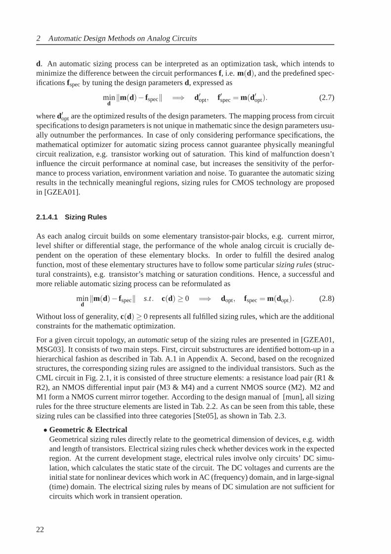
For a given circuit topology, anautomaticsetup of the sizing rules are presented in [GZEA01,MSG03]. It consists of two main steps. First, circuit substructures are identified bottom-up in ahierarchical fashion as described in Tab. A.1 in Appendix A.Second, based on the recognizedstructures, the corresponding sizing rules are assigned tothe individual transistors. Such as theCML circuit in Fig. 2.1, it is consisted of three structure elements: a resistance load pair (R1 &R2), an NMOS differential input pair (M3 & M4) and a current NMOS source (M2). M2 andM1 form a NMOS current mirror together. According to the design manual of [mun], all sizingrules for the three structure elements are listed in Tab. 2.2. As can be seen from this table, thesesizing rules can be classified into three categories [Ste05], as shown in Tab. 2.3.
• Geometric & ElectricalGeometrical sizing rules directly relate to the geometrical dimension of devices, e.g. widthand length of transistors. Electrical sizing rules check whether devices work in the expectedregion. At the current development stage, electrical rulesinvolve only circuits’ DC simu-lation, which calculates the static state of the circuit. The DC voltages and currents are theinitial state for nonlinear devices which work in AC (frequency) domain, and in large-signal(time) domain. The electrical sizing rules by means of DC simulation are not sufficient forcircuits which work in transient operation.
22

2.1 Automatic Circuit Sizing
Tabl
e2.
2:S
izin
gru
les
for
com
mo
n-m
od
e-lo
gic
cell
inF
ig.2
.1S
truc
ture
elem
ent
No.
Con
stra
int
Saf
ety
mar
gin
Rea
son
RW
1/L
1 I b1
I b2
Res
ista
nce
lo
ad
pair
R1
& R
2
RW
2/L
2
1R
W1,
2≥
mm
=1µ
mlim
itre
lativ
eva
rianc
eof
2R
L1,
2≥
mm
=1µ
mth
ere
sist
ance
fact
or3
RW
1=
RW
2sy
stem
atic
load
mat
ch4
RL
1=
RL
2
5V
DD−
R1,
2·I b
≤m
m=
0.4V
suffi
cien
tdra
in-s
ourc
evo
ltage
head
room
for
M2
curr
ents
ourc
e
VD
S4
VD
S3
VG
S4
VG
S3
NM
OS
di
ffer
ent
ial p
air
M3
& M
43
3/
WL
44
/W
L
I b
I b1
I b2
6V
GS
3,4−
Vth
3,4≥
mm
=10
mV
inve
rsio
n7
VD
S3,
4−
(VG
S3,
4−
Vth
3,4)≥
mm
=10
mV
satu
ratio
n8
L3,
4·W
3,4≥
mm
=1µ
m2
limit
Vth
mis
mat
ch9
L3,
4≥
mm
=0.
5µm
limit
rela
tive
varia
nce
of10
W3,
4≥
mm
=0.
5µm
the
tran
scon
duct
ance
fact
or11
VG
S3,
4−
Vth
3,4≤
mm
=1.
0Vre
duce
the
influ
ence
oftr
ansc
ondu
ctan
cem
ism
atch
onth
ein
puto
ffset
12−
m≤
VD
S3−
VD
S4≤
mm
=20
0mV
redu
ceth
ein
fluen
ceof
the
chan
nel
leng
thm
odul
atio
nfa
ctor
onth
ecu
rren
ttra
nsm
issi
onco
effic
ient
13L
3=
L4
avoi
dtr
ansc
ondu
ctan
cem
ism
atch
14W
3=
W4
and
inpu
toffs
etvo
ltage
mis
mat
ch
I b
VG
S1
VG
S2
VD
S1
VD
S2
NM
OS
curr
ent m
irror
M1
& M
2
11
/W
L2
2/
WL
I b
15V
GS
1,2−
Vth
1,2≥
mm
=10
0mV
inve
rsio
n16
VD
S1,
2−
(VG
S1,
2−
Vth
1,2)≥
mm
=10
0mV
satu
ratio
n17
L1,
2·W
1,2≥
mm
=1µ
m2
limit
Vth
mis
mat
ch18
L1,
2≥
mm
=0.
5µm
limit
rela
tive
varia
nce
of19
W1,
2≥
mm
=0.
5µm
the
tran
scon
duct
ance
fact
or20
−m≤
VD
S1−
VD
S2≤
mm
=20
0mV
redu
ceth
ein
fluen
ceof
the
chan
nel
leng
thm
odul
atio
nfa
ctor
onth
ecu
rren
ttra
nsm
issi
onco
effic
ient
21L
1=
L2
limit
syst
emat
icm
ism
atch
es
23

2 Automatic Design Methods on Analog Circuits
• Function & RobustnessFunctional sizing rules guarantee the elementary structures to operate the desired analogfunctions, e.g. M1 & M2 working in saturation for current mirror operation. Robustnesssizing rules define the design margin in order to decrease thesensitivity of analog perfor-mance due to the variation of process and of operation conditions, e.g. the minimal length-/width/area. The margin values in Tab. 2.2 are closely dependent on technology process.
• Equality & InequalityEquality sizing rules state that the design parameters havesame values or differ only by aconstant factor. In general, the equality relationship exists only for the geometric quantities,e.g. L1 = L2 in NMOS current mirror. Inequality sizing rules state the upper or lowerbounds of the electrical or geometric circuit quantities, e.g. VDS1≥ VGS1−Vth1 for M1 insaturation.
Table 2.3: Classification of the sizing rules on CML in Tab. 2.2Rules No. 1 2 3 4 5 6 7 8 9 10 11 12 13 14 15 16 17 18 19 20 21
Geometric * * * * * * * * * * * * * * *Electrical * * * * * *Function * * * * * *
Robustness * * * * * * * * * * * * * * * *Equality * * * * * * * * * * * * * * * * * *
Inequality * * * * * * * * * * * * * * * *
2.1.4.2 Automatic Sizing Flow
The design flow of a simulation-based automatic sizing process is briefly shown in Fig. 2.5.The starting point of the automatic sizing flow is the circuittopology in schematic including thecorresponding testbenches. By using the graphical interface, e.g. Virtuoso schematic editor ofCadence [Cada], the circuit netlist can be generated and be forwarded tospice-like simulator.By means of circuit simulation, the circuit behavior can be determined, including the circuitDC operation points, i.e. node voltages and branch currents, AC (small-signal) performances,e.g. DC gain and phase margin, and transient (large-signal)performances, e.g. delay and slewrate. The geometric sizing rules are configured according tothe circuit netlist, and the electricalsizing rules are evaluated by means of the DC simulations.
The performances to be optimized and their corresponding specifications are the inputs of thecost-function (objective-function) generator. With the help of mathematical optimization al-gorithm, circuit optimizer can find a set of design parameters after several optimization loops.The obtained circuit performances can fulfill their specifications. The cost function and theoptimization method have big effect on the time cost of the sizing process and the quality ofthe final results. Although the cost functions appearing in analog circuit are nonlinear with po-tential local minimum, experimental results show that the deterministic method performs well,e.g. sequential quadratic programming (SQP) algorithm. Anacceptable amount of the startingpoints result in good solutions while the optimization timeis kept in a reasonable cost. Thedetailed realizations of cost functions and optimization algorithms are beyond the scope of thisthesis.
24

2.2 Performance Space Exploration
The design parameters are the variables of the optimization. The upper and/or lower bounds ofthe design parameters should be predefined. For example, theminimal and the maximal limitsof transistor dimensions are set to avoid any unrealistic physical implementation.
In the simulation-based automatic sizing method, circuit performances need to be newly eval-uated in each optimization loop, so a mass of simulations arerequired. In order to acceleratethe sizing process, the simulation tasks can be distributedonto a cluster of workstations andbe executed in parallel. A master machine is in charge of collecting the simulation results andcontrols the optimization process.
The automatic sizing method provides an automatic mapping process from circuit specificationsto design parameters. Currently, the simulation-based automatic sizing method is successfullyapplied to some analog circuits, e.g. OP AMP design, whose sizes are less than 20-30 devicesand the self performance evaluations (simulations) are fast.
2.2 Performance Space Exploration
As we know, circuit simulation provides an automatic mapping process from design parametersto circuit performances. Compared to the mapping from one design point to one performancepoint, performance space exploration (PSE) intends to find the whole feasible performancespace for a given circuit topology and process technology.
2.2.1 Feasible Parameter Space
There exists geometric limitations for each device, i.e. the lower or/and the upper bounds forlength/width of devices. For example in 110nm CMOS process technology, the smallest physi-cal channel length(Lmin) of CMOS is 110nm. Generally in analog design, the minimal lengthsof transistors are set at least 1.2∗Lmin, while the maximal bounds for length and width preventthe devices from excessively large. Forn-number design parameters, the initial design parame-ter space is and-dimension parameter space. Each geometrical point in the initial whole spacecan be mathematically interpreted as a vector of design parametersd ∈ R
nd . In practice, thesizing rules in Sec. 2.1.4.1 separate the whole design spaceinto two nonoverlapping subspaces:one parameter subspace where the associated sizing rules are violated (c(d) < 0) and the otherparameter subspace where the sizing rules are satisfied (c(d) ≥ 0). The subspace, where allsizing rules are fulfilled, is calledfeasible parameter spaceD ⊂ R
nd , i.e.
D = d | c(d) ≥ 0, c(d) ∈ Rq, d ∈ R
nd . (2.9)
Fig. 2.6 illustrates the feasible parameter spaceD for R2.
To decrease the optimization complexity, less design variables are wanted. Through equalitysizing rules, the explicitly algebraic relationships of the correlated design parameters are known.In consequence, the dimension of the design space can be decreased algebraically. It is worthyto mention that only the reduced design parameters are considered throughout this thesis. With
25

2 Automatic Design Methods on Analog Circuits
Circuit topology (Including test bench)
Circuit netlist
Spice-like simulator
Sizing rules(e.g. saturation, matching)
Large-signal perf. (e.g. delay, slew rate)
Small-signal perf. (e.g. DC gain, phase margin)
Geometric rules
Electrical rules
Cost-function generator
Circuit optimizer
Circuit specifications
Sized circuit
workstations
Specifications satisfied?
Yes
No
Finished
Design parameters
(e.g. transistor w/l)
Performances
Distributation of simulation tasks
master
Figure 2.5: Design flow of the automatic sizing process
d1
d2
du1dl1
du2
dl2
d1
d2
D
du1dl1
du2
dl2
Figure 2.6: Feasible parameter spaceD
26

2.2 Performance Space Exploration
the reduced design parameters, all inequality sizing rulescan be reformulated asc(d) ≥ 0, asingle nonlinear vector inequality interprets the combination of all the sizing rules
c(d) ≥ 0 =⇒ ∀i ∈ 1, ...,q
ci(d) ≥ 0, (2.10)
whereq is the total number of sizing rules and the indexi denotes thei-th entry of the vector.
2.2.2 Feasible Performance Space
Based on the feasible parameter spaceD , the feasible performance spaceF ∈ Rnf can be ob-
tained from the mappingm(·), which expressed as
F = f | f = m(d)∧d ∈ D , d ∈ D =⇒ c(d) ≥ 0. (2.11)
Each feasible parameter vectord can generate a performance value. The wholefeasible perfor-mance spacecan be obtained by means of pointwise simulation. However, too many simula-tions are needed to find the whole range ofF . It would be more effective to search only for theboundary ofF , ∂F , instead of the entireF . It is worth noting that∂F is not the mapping ofthe boundary ofD , ∂D , generally.
d1
d2
f = m(d)
f1
f2
FD
D F
Figure 2.7: Feasible performance spaceF
The knowledge of the feasible performance space is extremely useful for designers [Ste05]:
• For a given technology and circuit topology, the feasible performance space presents thecircuit ultimate capabilities without violating any sizing rules. Various circuit topologiescan be easily compared with each other. The advantages and disadvantages of each topologycan be accurately evaluated by the comparison on their feasible performance spaces.
• Feasible performance space offers a whole insight into the circuit performance, while tra-ditional optimization method generates only one optimizedresult. Hence, analog designershave more overview on the circuit capability, and can deliberately select an compromisedoptimal result among the conflicting performances.
• In a hierarchical design process on a large-scale analog/mixed signal circuit, feasible perfor-mance space can be taken as the additional design constraints for the higher-level design.Considering the performance capability of the lower-levelcircuit can avoid any iterationsteps, e.g. redefinition on specifications of subblock.
27

2 Automatic Design Methods on Analog Circuits
2.2.3 Performance Space Exploration
The goal of performance space exploration (PSE) is to find a description ofF in the perfor-mance space. In Equation 2.11, the feasible performance space F is coupled to the feasibleparameter spaceD . Since the performancesf1, . . . fn to be optimized are usually competingwith each others, circuit sizing becomes a multi-objectiveoptimization problem [LTZ79] overthe design parameterd under salification with certain sizing rulesc(d) ≥ 0, mathematicallyexpressed as
maxd
f , m(d) ,
m1(d)...
mn(d)
s.t. c(d) ≥ 0 =⇒ d∗, f∗ = m(d∗). (2.12)
In practice, it is rarely possible to find a set of design parameters that can improve all perfor-mances simultaneously. A trade-off situation mostly occurs among performances, where oneperformance is improved at the cost of other performances. This phenomenon introduces theconcept ofPareto Optimality[HM79, LTZ79]. A set of performancesfa is considered moreoptimal than a set offb, if fa dominatesfb, i.e.
fa ≻ fb ⇔ ∀i ∈ 1, ...,n
(fa,i > fb,i) ∧ ∃i ∈ 1, ...,n
(fa,i > fb,i). (2.13)
A Pareto optimal point is a set of performancesf∗ which is not dominated by any other setf. Allof the Pareto optimal points compose of aPareto-optimal frontof the performance. Generally,the points on the Pareto-optimal front are also calledefficient points. A 2D Pareto-optimal frontfor the two performancesf1 and f2 is shown in Fig. 2.8. The shaded area shows the feasibleperformance spaceF .
Performance space exploration is a computationally expensive process. Under the compro-mise between accuracy and time cost, a deterministic PSE method, i.e. Normal-BoundaryIntersection (NBI) method is adopted in this thesis. NBI method is fit for high accuracy andlow-dimensional performance exploration.
2.2.3.1 Normal-Boundary Intersection
The Normal-Boundary Intersection in [SGA03] is a two-step process. In the first step, theindividual maxima (IM)f∗i , where the individual performancefi shows its global maximaf ∗i ,are determined by maximizing the following objective function oIM ,i :
maxd
[oIM ,i , mi(d)] s.t. c(d) ≥ 0, i = 1, . . . ,nf
=⇒ d∗, f ∗i = mi(d∗), f∗i = m(d∗).(2.14)The
IM build up the matrixF:F = [f∗1 · · · f∗nf
]. (2.15) Optimization is formulated as maximization. Minimizationcan be included by maximization of the negativevalues.
28

2.3 Summary
f1
f2
f1*
f2*
0
1
⋅
F
n
0.5
0.5
⋅
F
1
0
⋅
F
Pareto-optimal front
F
H
Figure 2.8: Normal boundary intersection [SGA03]
It is easy to know that these global maxima are the boundary points of the Pareto-optimal front.And the efficient points should locate between these IMs. Assume a polyhedronH connectswith the individual IMs as its corner points. The key idea of NBI is to search for efficient pointsby starting from the points onH and going along the linesn, which are perpendicular toH anddirect away from origin. If the respective portion of∂F is convex, the search results in Pareto-optimal points. Moreover, when the starting points are evenly distributed overH , the foundefficient points are also well-placed on the Pareto-optimalfront. In fact, the searching directionis not necessary to be exactly perpendicular toH . The quasi-normal vectorn is calculated by
n = f∗1+ · · ·+ f∗nf. (2.16)
The efficient points are the best performance set of the circuit under satisfying the sizing rules:
maxd,λ
λ s.t. F ·w+λ ·n = f(d) ∧ c(d) ≥ 0, (2.17)
wherew is the set of weightsw = [w1w2 · · ·wJ]T and
J
∑j=1
w j = 1 and w j > 0 for j ∈ 1, ...,J. (2.18)
Fig. 2.8 illustrates the method fornf = 2 andJ = 3. The pointsF ·w lie on the connecting lineof the individual minima in the 2D case.
2.3 Summary
In this chapter, two automatic design methods for analog design have been described, i.e. thetop-down automatic sizing process and the bottom-up performance space exploration.
29

2 Automatic Design Methods on Analog Circuits
For automatic sizing process, the sizing rules are used to prevent the automatically sized circuitsfrom senseless results. The design flow of the simulation-based automatic sizing method arediscussed. Since performance evaluation is by means of circuit-level simulation, this method isfeasible only for small analog circuit design currently.
For performance space exploration, [SGA03, SG03, Her03, SGA04, MSGS05] focus on howto efficiently and accurately perform PSE by means of statistical or deterministic, simulation-based or equation-based methods. A normal-boundary intersection method is applied in thisthesis to generate Pareto-optimal fronts.
In the next chapter, how to embed both analog design methods into the proposed hierarchicaloptimization process will be introduced.
30

Chapter 3
Proposed Hierarchical OptimizationMethodology
For a large-scale analog/mixed-signal circuit, a comprehensive hierarchical optimizationmethodology is proposed in this thesis. Both analog design methods discussed in Chapter 2,i.e. automatic sizing process and performance space exploration, are well integrated in thismethodology. The details of the design flow are described in this chapter.
First of all, let we discuss why hierarchical optimization process is needed and a flat simulation-based optimization method is not feasible for a large-scaleanalog/mixed signal circuit. Themain reasons are the following two factors:
• Time cost:A circuit-level simulation on large-scale analog/mixed signal circuit by usingnumerical simulator is a huge time-consuming process. It iswell known that higher simu-lation accuracy is achieved by setting smaller step size in numerical simulators. Althoughthe accuracy requirements (i.e. step size in the simulationsetup) could be different for eachblock, so long as all blocks are simulated together, the stepsize of the numerical simulatorhas to be set small enough to provide an accurate evaluation on the whole circuit. Hence,the common step size is configured as the cut set of all individual step sizes. Why does asingle transient simulation (large-signal analysis) of a phase-locked loop last hours or days?Let’s have a look at one example in Fig 3.1, the states (voltages/currents) of the blocksCPandPFD need to be updated every 20ps and 30ps respectively. However, the common stepsize of the simulation has to be smaller than 8ps because the update rate of the blockVCOis 8ps. Consequently, many computations on the blocksPFD andCP are redundant, whichresults in more computing cost and longer simulation time.
• Optimization complexity:The design space and the optimization complexity increasesex-ponentially with the number of design parameters. If all blocks are simultaneously opti-mized at once, the optimization complexity will become extremely high due to the largenumber of design parameters.
31

3 Proposed Hierarchical Optimization Methodology
1 =20ps 2 =8ps 3 =30psCP PFDVCO
common (1,2,3)
Figure 3.1: Step sizes in numerical simulation
3.1 Hierarchical Top-Down Circuit Sizing
Traditional bottom-up sizing method is not efficient for thedesign of a complex analog/mixed-signal circuit. One of the most common problem is failure to meet the initial system require-ment, which is usually caused by the loose definition of specifications for building blocks. Ahierarchical top-down sizing method is adopted to address this issue. The basic idea is that thewhole system is partitioned into subsystems, which are further decomposed into smaller func-tion blocks. Based on the initial requirements on the whole system, the respective specificationsof each subsystem are first derived by the high-level design.Then, each function block is builtin order to fulfill the subsystem requirements. Finally, allparts of system are integrated togetherand are verified with respect to the original requirements.
The definition of the each hierarchical level is closed dependent on the design system and itscomplexity. The number of hierarchical level could be threeor even more. In this thesis, onlytwo design-levels are considered in hierarchy. Fig 3.2 shows a two-level hierarchical decom-position of an analog/mixed-signal system, i.e. system level and circuit level. At the top of thehierarchy, the entire system performance can be expressed as
f = [ f1, f2, f3, . . .]T . (3.1)
System-Level Parameters The entire system is partitioned intoα = A,B, . . . building blocks.The performances ofα building block, which do have effect on the system performances, arenoted aspT
α. The whole system-level parameters can be expressed as
p = [pTA, pT
B, . . . ]T . (3.2)
System-Level Simulation The system-level simulation provides a mapping of the system-level parameters onto the system performances:p 7→ f. The simulation on system level runson behavioral models, which represent circuit function in special languages instead of the de-tailed device models. Normally, the simulation based on behavioral models is very fast, so thesimulation-based automatic sizing method is feasible on system-level design.
32

3.1 Hierarchical Top-Down Circuit Sizing
Automatic Sizing on System Level System performances are optimized subject to system-level constraints by sizing of the system-level parametersp:
maxp
f s.t. c(p) ≥ 0
=⇒ popt, fopt = m(popt),(3.3)with
c(p) = cs(p) ≥ 0 ∧ cpα(pα) ≥ 0, α = A,B, . . .. (3.4)
The system-level constraintc(p) includes two aspects: 1) the necessary design constraints forsystem itself:cs(p) ≥ 0, e.g. system stability criterion; 2) a pure top-down refinement of speci-fications may easily produce overambitious block specifications if the performance capabilitiesof the underlying analog circuit implementations are not taken into account. Consequently, low-level physical effects have to be propagated bottom-up. At system-level sizing, it is necessaryto have a description of the performance capabilities of theeach functional block:cpα(pα) ≥ 0.
Circuit-Level Parameters At the circuit level, parameters such as transistor dimensions, re-sistance, capacitance, inductance and bias voltage/current are assigned to the design parametersof α building block at circuit level, expressed as
xα = [W1,L1,W2,L2, . . . ,C,R, Ibias, . . .]T . (3.5)
Circuit-Level Simulation Circuit simulation provides a mapping of the circuit-levelpara-meters onto the circuit-level performances, i.e. the system-level parameters:xα 7→ pα,α =A,B, . . . ,Z. Normally, the simulation of each building block is very fast, so the simulation-based automatic sizing method is feasible on circuit-leveldesign of each building block.
Automatic Sizing on Circuit Level The optimized values of system-level parameters, i.e.popt, are propagated to the performance specifications of circuit-level. These specifications areachieved by the final circuit-level results,xopt. The automatic sizing process onα building blockcan be formulated as
minxα
‖m(xα)−popt‖ s.t. cxα(xα) ≥ 0, α = A,B, . . .
=⇒ xopt, popt = m(xopt).(3.6)
cxα(xα)≥0 is the circuit-level sizing constraints. The automatic sizing processes for all buildingblocks can be executed in parallel.
In the hierarchical sizing process, we start with system specifications, follow the top-downpropagation of the specifications, and end up with a fully sized circuit implementation on cir-cuit level. Since the performance capabilities of the underlying analog physic implementationsare already taken into account, a first-time-successful top-down sizing process can be realizedconsequently.
33

3 Proposed Hierarchical Optimization Methodology
Block APA
Block BPB
Block P
transisor W/L
Whole Circuitf = [f1, f2, f3, ... , fn]
transisor W/L
System level
transisor W/L
Circuit level
Figure 3.2: Hierarchical sizing of a large-scale analog/mixed-signalcircuit
3.2 Pareto-Optimal Front in Hierarchical Optimization
Performance space exploration (PSE) transforms technological constraints bottom-up into fea-sible performance spaces. Therefore, the feasible region of system-level parameterspα, i.e.cpα(pα) ≥ 0 can be defined by PSE method onα block. Since PSE is a computationally ex-pensive process, is it really necessary to know the entire feasible region of circuit performancesfor the optimization at system level? Most of current PSE methods are proposed to find thePareto-optimal front instead of the entire feasible region. In practice, Pareto-optimal front issufficient for the system-level optimization.
In analog circuits, a circuit performance has normally the monotone relationship with one de-sign parameter. For example in Fig. 1.3(a), DC gain becomes larger with a larger width ofthe input NMOS, slew rate increases with the increasing biascurrent or with the decreasingcompensation capacitance. The performances of PLLs in Chapter 4 and of A/D convertersin Chapter 5 satisfy the monotone relationship with their design parameters. To simplify the-ory analysis, a two-dimensional design spacex = (x1,x2) and a maximization problem with atwo-dimension objective spacef = ( f1(x1,x2), f2(x1,x2)) are taken here as an example. Sup-pose there exists a dominated point(x⋄1,x
⋄2) in design parameter space, which contributes to an
efficient point on the Pareto-optimal front in the objectivespace. However, this assumptionconflicts with the essential definition of the Pareto-optimal front. For the point(x⋄1,x
⋄2), there
exists a point(x∗1,x⋄2), whosex∗1 dominatesx⋄1. It results in
x∗1 ≻ x⋄1 =⇒ f1(x∗1,x
⋄2) ≻ f1(x
⋄1,x
⋄2) ∧ f2(x
∗1,x
⋄2) ≻ f2(x
⋄1,x
⋄2)
=⇒ f(x∗1,x⋄2) ≻ f(x⋄1,x
⋄2).
(3.7)
Or there exists a point(x⋄1,x∗2), whosex∗2 dominatesx⋄2, it results in
x∗2 ≻ x⋄2 =⇒ f1(x⋄1,x
∗2) ≻ f1(x
⋄1,x
⋄2) ∧ f2(x
⋄1,x
∗2) ≻ f2(x
⋄1,x
⋄2)
=⇒ f(x⋄1,x∗2) ≻ f(x⋄1,x
⋄2).
(3.8)
Therefore, for a dominated design pointx⋄ and the corresponding performancef⋄, there exists
34

3.3 Behavioral Modeling
definitely a dominating pointx∗ and its corresponding dominating performancesf∗. In the hier-archical design, the circuit-level performances are used as design variables at the system level.Hence, an optimal system-level performance should be generated by the design points lying onthe Pareto-optimal front of the circuit level. This is coincident with the conclusion in [EMG05].A lower-level solution moving towards its Pareto-optimal front should result in a movement ofits corresponding higher-level solution towards the higher-level Pareto-optimal front, as visual-ized in Fig. 3.3. According to the conclusion, the system-level parameterspα can be restrictedon the Pareto-optimal front ofα block during the system-level optimization.
System
Block A Block B Block
feasible region
Pareto-optimal front
Block C ......
Figure 3.3: Pareto-optimal fronts in hierarchical optimization
3.3 Behavioral Modeling
By using a numerical simulator, circuit-level simulation based on the BSIM device model isaccurate but requires huge computational time cost, which is not practical for the optimizationprocess. As the number of design parameters and the complexity of analog/mixed signal circuitscontinue to increase, circuit-level simulation is and willcontinue to be a critical issue for de-signers. An alternative to the circuit-level simulation, more efficientbehavior-level simulationis becoming popular and gradually accepted by analog designers. Behavior-level simulationusesbehavioral models, "that reflect the terminal characteristics of functions realized by cir-cuits rather than the circuit level (transistor-level) details of the circuit " [CPH94].
Behavioral models can be applied not only to bottom-up verification process but also to top-down design process. At the beginning design phase of a large-scale analog/mixed signal circuit,it is more efficient and economical to use behavior-level simulations to check design conceptsand to explore several system architectures, instead of undertaking the detailed final circuit real-ization. At the final design phase, behavioral models can obviously reduce the verification time.This thesis focuses on the application of behavioral modelsin the top-down design process.
35

3 Proposed Hierarchical Optimization Methodology
Should the behavioral model exactly or approximately represent the electronic functions of thecircuit? A compromised decision has to be made between simulation cost and model accu-racy. On the one hand, behavioral model describes a circuit functionality with relatively fewcomponents, making simulation much faster. On the other hand, a behavioral model includesmore secondary circuit effects, presenting more accurate circuit behavior but making simulationslower. To achieve a good balance between computational efficiency and performance accuracy,the proper CAD tools are required which well cooperate with the behavioral models. Two mostpopular modeling methods in analog/mixed-signal design are briefly described in the following.
3.3.1 Modeling in Hardware Description Languages
Hardware description languages (HDLs) are programming languages designed to describe thebehavior of physical devices and processes. Behavioral models written in various kinds ofHDLs have their corresponding suitable simulators. Two mixed-signal hardware descriptionlanguages, VHDL-AMS [VHD] and Verilog-AMS [Vera] are developed for high-level verifica-tion∗ on large-scale analog/mixed-signal systems. The commercial tools used are the Advance-MS simulator from Mentor Graphics [Men] for VHDL-AMS and theAMS Simulator fromCadence Design Systems [Cada] for Verilog-AMS. As indicated by their names, both mixed-signal simulators and HDLs can applied not only on digital circuits but analog circuits as well.The simulators are capable of simulation on pure circuit-level simulations, or on pure behavior-level simulations, or on mixed-level simulation (some blocks are circuit realization, while oth-ers are behavioral modules). Both digital and analog designshare the same design environmentand flow, which provides a straight-forward method to use behavioral models and improvesdesign efficiencies. VHDL-AMS and Verilog-AMS describe complex continuous analog sys-tems in form of differential algebraic equations (DAEs), which enables numerical simulatorsto evaluate the behavioral models like the usual device models. Additionally, they inherit theevent-driven capability from digital simulator engines and allow analog event-driven models foranalog simulation [CB99].
A VHDL-AMS model consists of one entity and one or more architectures, as shown inFig 3.4(a). Theentity specifies the interface of the model to the outside circuits.It includesthe description of the model ports (the input/output pins that connect to other models) andthe definition of its generic parameters. Fig 3.4(b) shows a mode of an ideal OP AMP withslew-rate limiting. There are two inputs (plus_in, minus_in) and one output (vout). VHDL-AMS introducesquantity to represent the unknown variables in the DAEs. Thearchitecturecontains the detailed implementation of the model, which can have three different styles: 1)Structure style is a description on the netlist connectionsof the elementary models. 2) Behav-ioral style is a transformation description from inputs to outputs by means ofconcurrent state-mentsor/andsimultaneous statements. 3) A style combines structural and behavioral elements.Simultaneous statements describe the continuous behaviorby differential algebraic equations.Concurrent statements describe event-driven behaviors, e.g. concurrent signal assignment andprocess assignments like digital modeling. More details onVHDL-AMS modeling can be foundin [CB99,APT02].
∗ "It is important to recognize that the AMS languages are primarily for verification. Unlike the digital languages,the AMS languages will not be used for synthesis in the foreseeable future because the only synthesis that isavailable for analog circuit is very narrowly focused" [KHC+01].
36

3.3 Behavioral Modeling
Architecture 1 simultaneous statements
concurrent statements
Library ieee_proposed; use ieee_poposed.electrical_systems_all;entity opamp is; generic (gain: real : = 50; port terminal plus_in, minus_in,
output : electrical;end entity amplifier;
architecture slew_limited of opamp is quantity v_in across plus_in to minus_in; quantity v_out across i_out through output; quantity v_amplified : voltage;begin v_amplified == gain * v_in v_output == v_amplifed’slew(1.0e6, -1.0e6);end architecture slew_limited;
Entity generic definition port definition
Architecture 2
Architecture 3
(a) (b)
Figure 3.4: (a) Basic structure of VHDL-AMS Model (b) A VHDL-AMS Model ofan idealOP AMP with slew-rate limiting [APT02]
3.3.2 Modeling in Simulink
Simulink is a companion of MATLAB, developed by the MathWorks [Mat]. A user friendlygraphical interface is available for building models, which makes it easier to maintain anoverview of the system and subblocks. Simulink includes a comprehensive library of stan-dard models, e.g. sinks, sources, linear and nonlinear components. Designers can create andcustomize their own blocks by assembling models directly using these standard blocks or cod-ing in MATLAB m-files. Moreover, simulink has built-in ordinary differential equation (ODE)solvers, which are automatically configured multi-rate at run-time of each model, i.e. that dif-ferent parts are sampled or updated at different rates.
A behavioral model example of an integrator in Simulink, which includes its non-idealities, isshown in Fig. 3.5 [MBF+03]. In the model, the limited slew rate and the limited bandwidthperformances are modeled in “GBW & SR” MATLAB function. The limited gain is modeledthrough that only fractionα of the previous integrator output is added to each new input sample.The limited output range can be simply modeled by using a saturation block inside the feedbackloop of the integrator. As we can seen from this example, all behavioral modules for sub-building block are already available in Simulink’s library, the work for designers is to constructmore complex models based on these fundamental cells.
Because of its strong capability and convenient use interface, Simulink is widely adoptedin modeling tasks. However, Simulink is difficult to be integrated into the current popu-lar analog/mixed-signal circuit design environments, e.g. Advance-MS [Men] and VirtuosoAMS [Cada]. While the behavioral modeling in HDLs is in the same design environment ascircuit design, it is more convenient for designers to buildup model, design circuit and simu-
37
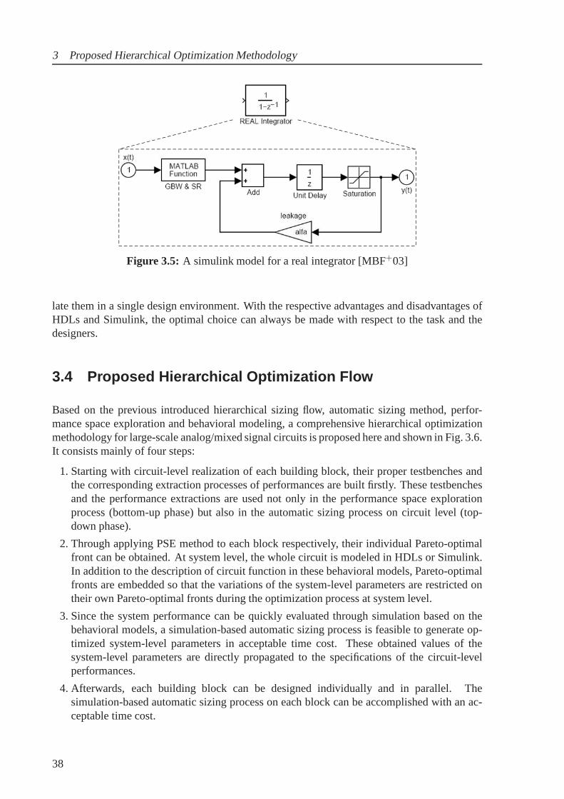
3 Proposed Hierarchical Optimization Methodology
Figure 3.5: A simulink model for a real integrator [MBF+03]
late them in a single design environment. With the respective advantages and disadvantages ofHDLs and Simulink, the optimal choice can always be made withrespect to the task and thedesigners.
3.4 Proposed Hierarchical Optimization Flow
Based on the previous introduced hierarchical sizing flow, automatic sizing method, perfor-mance space exploration and behavioral modeling, a comprehensive hierarchical optimizationmethodology for large-scale analog/mixed signal circuitsis proposed here and shown in Fig. 3.6.It consists mainly of four steps:
1. Starting with circuit-level realization of each building block, their proper testbenches andthe corresponding extraction processes of performances are built firstly. These testbenchesand the performance extractions are used not only in the performance space explorationprocess (bottom-up phase) but also in the automatic sizing process on circuit level (top-down phase).
2. Through applying PSE method to each block respectively, their individual Pareto-optimalfront can be obtained. At system level, the whole circuit is modeled in HDLs or Simulink.In addition to the description of circuit function in these behavioral models, Pareto-optimalfronts are embedded so that the variations of the system-level parameters are restricted ontheir own Pareto-optimal fronts during the optimization process at system level.
3. Since the system performance can be quickly evaluated through simulation based on thebehavioral models, a simulation-based automatic sizing process is feasible to generate op-timized system-level parameters in acceptable time cost. These obtained values of thesystem-level parameters are directly propagated to the specifications of the circuit-levelperformances.
4. Afterwards, each building block can be designed individually and in parallel. Thesimulation-based automatic sizing process on each block can be accomplished with an ac-ceptable time cost.
38

3.4 Proposed Hierarchical Optimization Flow
Performance space exploration engine
Test bench & performance extraction
AB
B
Pareto-optimal front
AB
Behavioral model(1) Circuit function description(2) Pareto-optimal front
A
B
Bottom-Up Extraction Top-Down Sizing
System performancef=[f1,f2,f3, ... ,fn] to be optimized
Automatic sizing engine
Optimized system-level parameterspopt=[pT
opt@A,pT
opt@B,pT
opt@, ... ]
Specifications of circuit-level performance of building block A
Automatic sizing engine
B
Optimized circuit-level parameters of building block A B
A
Building block
Cir
cuit
Lev
elSy
stem
Lev
el
Figure 3.6: Proposed hierarchical optimization design flow
In summary, the proposed hierarchical optimization methodology is characterized by a bottom-up extraction process of circuit capability and a top-down hierarchical automatic sizing process.
39

3 Proposed Hierarchical Optimization Methodology
3.5 Hierarchical Optimization based on Worst-Case-AwarePareto-Optimal Front
The Pareto-optimal fronts extracted from the most current PSE methods [SGA03, SGA04,EMG05, MSGS05] are nominal Pareto-optimal fronts, which consider only design parameters.As device sizes shrink, the effect due to the variations of statistical parameters and of operationparameters becomes more and more pronounced in analog design. The nominal Pareto-optimalfronts cannot represent the actual capability of the circuit after fabrication. Generally, it willresult in a poor yield if a nominal design point lies in the tail of the performance distribution.Therefore, ayield-awarePareto-optimal front (points on the front guaranteeing a fixed yieldnumber) would be very useful for improvement on production yield.
In [TTR06], a solution generates firstly the nominal Pareto-optimal fronts, and then combineswith Monte Carlo approximation to computeyield-awarePareto-optimal fronts. Compared tothe high computational cost Monte Carlo analysis,worst-case analysisis applied to extract aworse-case-awarePareto-optimal front (design point on the front guaranteeing a target yieldnumber even under the worst-case operation condition) in this thesis.
Worst-Case Analysis The following discussion of worst-case analysis is based onone per-formance. Worst-case analysis takes into account fluctuations in the fabrication process andchanges in the operating condition. Therefore, statistical parameters and operational parame-ters are considered through the worst-case analysis, whereas design parameters remain constant.In consequence,
d∗ = const and c(d∗) = const (3.9)
holds throughout the worst-case analysis.
Worst-case analysis (WCA) [AGC94] intends to find the lowestperformance value that is ob-tained for a given design parameter setp∗, a given tolerance regionTθ of operation parametersand a given tolerance regionTs of statistical parameters:
mins,θ
f(d∗,s,θ) s.t. s∈ Ts, θ ∈ Tθ, (3.10)
where Tθ = θ|θL ≤ θ ≤ θU (3.11)
Ts = s| ‖s‖2C = (s−so)
TC−1(s−s0) ≤ β2w. (3.12)
θL , θU define the lower and upper boundaries of the operation parameters. The circuit ro-bustnessβw describes a weighted distance of the nominal design points0 in the space of thestatistical parameterss. ‖s‖2
C represents a tolerance ellipsoid according to the statistical pa-rameter distribution, whereC is the covariance matrix of statistical parameters. As we know,there always exists a matrixG, such that the transformed statistical parameterG(s−s0) followsthe distribution ofN(0,1) [Pap91], as depicted in Fig. 3.7 and given by
‖s−s0‖G = ‖G(s−s0)‖ =
√
(s−s0)TGTG(s−s0) (3.13)
C−1 = GTG. (3.14)
40
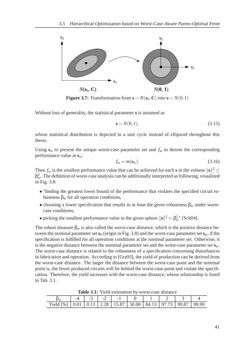
3.5 Hierarchical Optimization based on Worst-Case-Aware Pareto-Optimal Front
s2
s1
N(s0, C)
s2
s1
N(0, 1)
Figure 3.7: Transformation froms∼ N(s0,C) into s∼ N(0,1)
Without loss of generality, the statistical parameters is assumed as
s∼ N(0,1), (3.15)
whose statistical distribution is depicted in a unit cycle instead of ellipsoid throughout thisthesis.
Using sw to present the unique worst-case parameter set andfw to denote the correspondingperformance value atsw:
fw = m(sw). (3.16)
Then fw is the smallest performance value that can be achieved for eachs in the volume‖s‖2 ≤β2
w. The definition of worst-case analysis can be additionally interpreted as following, visualizedin Fig. 3.8:
• "finding the greatest lower bound of the performance that violates the specified circuit ro-bustnessβw for all operation conditions,
• choosing a lower specification that results in at least the given robustnessβw under worst-case conditions,
• picking the smallest performance value in the given sphere‖s‖2 = β2w" [Sch04].
The robust measureβw is also called theworst-case distance, which is the positive distance be-tween the nominal parameter sets0 (origin in Fig. 3.8) and the worst-case parameter setsw, if thespecification is fulfilled for all operation conditions at the nominal parameter set. Otherwise, itis the negative distance between the nominal parameter set and the worst-case parameter setsw.The worst-case distance is related to the robustness of a specification concerning disturbancesin fabrication and operation. According to [Gra93], the yield of production can be derived fromthe worst-case distance. The larger the distance between the worst-case point and the nominalpoint is, the fewer produced circuits will lie behind the worst-case point and violate the specifi-cation. Therefore, the yield increases with the worst-casedistance, whose relationship is listedin Tab. 3.1.
Table 3.1: Yield estimation by worst-case distanceβw -4 -3 -2 -1 0 1 2 3 4
Yield [%] 0.01 0.13 2.28 15.87 50.00 84.13 97.73 99.87 99.99
41
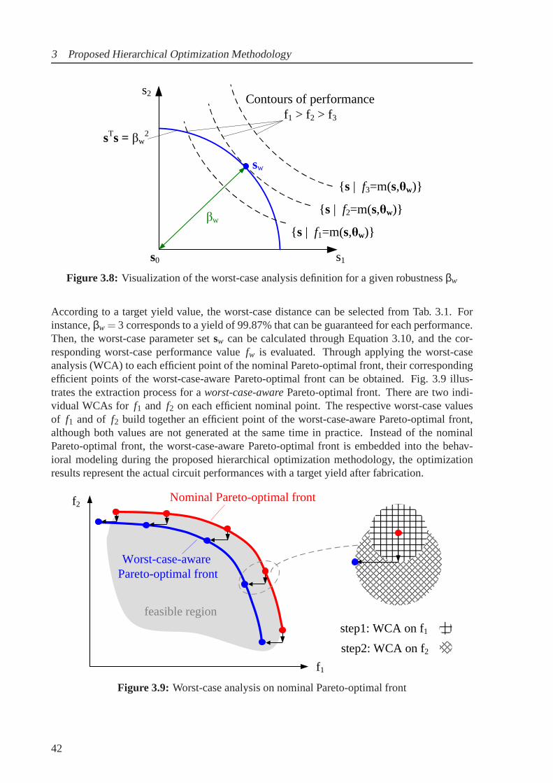
3 Proposed Hierarchical Optimization Methodology
s1
s2
s | f3=m(s,w)
s | f2=m(s,w)
s | f1=m(s,w)w
sw
Contours of performance f1 > f2 > f3
sTs = w2
s0
Figure 3.8: Visualization of the worst-case analysis definition for a given robustnessβw
According to a target yield value, the worst-case distance can be selected from Tab. 3.1. Forinstance,βw = 3 corresponds to a yield of 99.87% that can be guaranteed for each performance.Then, the worst-case parameter setsw can be calculated through Equation 3.10, and the cor-responding worst-case performance valuefw is evaluated. Through applying the worst-caseanalysis (WCA) to each efficient point of the nominal Pareto-optimal front, their correspondingefficient points of the worst-case-aware Pareto-optimal front can be obtained. Fig. 3.9 illus-trates the extraction process for aworst-case-awarePareto-optimal front. There are two indi-vidual WCAs for f1 and f2 on each efficient nominal point. The respective worst-case valuesof f1 and of f2 build together an efficient point of the worst-case-aware Pareto-optimal front,although both values are not generated at the same time in practice. Instead of the nominalPareto-optimal front, the worst-case-aware Pareto-optimal front is embedded into the behav-ioral modeling during the proposed hierarchical optimization methodology, the optimizationresults represent the actual circuit performances with a target yield after fabrication.
f1
f2
feasible region
step2: WCA on f2
step1: WCA on f1
Nominal Pareto-optimal front
Worst-case-aware Pareto-optimal front
Figure 3.9: Worst-case analysis on nominal Pareto-optimal front
42

Chapter 4
Hierarchical Optimization of Charge-PumpPhase-Locked Loops
Phase-locked loops (PLLs) provide well-timed on-chip clock signals for various applicationsin areas such as communications, wireless systems, dynamicrandom access memory and diskdrive electronics. Compared to the design concept of phase locking has almost keep same sinceit was invented in the 1930s, the design and implementation of PLLs have always developedwith the progress of the ICs. The requirements on PLLs becomes more and more stringent,such as accurate clock timing, less power consumption and small area, robust noise rejection.Due to the PLL’s circuit complexity, the optimization task of PLL is big challenge even forexperienced analog designers. Currently, there are two strategies for optimization to design highperformance PLLs. One way is through heuristic circuit topologies [Man96,Man03,WTHN04,CA05,KLK05]. The other way is through tuning design parameters for a given circuit topology[CPH+03, TVRM04, ZMG+05, TTR06, ZMGS06]. In this thesis, the second way is adopted.By using the proposed hierarchical optimization methodology in Chapter 3, an efficient designprocess for PLLs can be realized in an acceptable time cost.
In this chapter, Sec. 4.1 introduces the fundamentals of PLLs. Sec. 4.2 reviews the analysison PLL systems and Sec. 4.3 lists out some performances of PLLand summarizes the majordesign trade-offs. Sec. 4.4 shows the details of the proposed hierarchical optimization methodon a charge-pump phase-locked loop (CPPLL). Sec. 4.5 gives acomprehensive performancespace exploration (PSE) on a whole CPPLL system. Finally, Sec. 4.6 concludes.
4.1 CPPLL Fundamentals
4.1.1 PLL Introduction
The primary function of phase-locked loops is to generate anoutput clock whose phase is lockedto the phase of the input reference clock. In contrast to conventional feedback circuits operateon voltage/current amplitudes or their changing rate, PLL feedback systems work on signal’sphases. The operation of PLLs is briefly described as follows. More details can be foundin [Raz96,Raz01,Bes03].
43

4 Hierarchical Optimization of Charge-Pump Phase-Locked Loops
The basic building blocks of a typical PLL consists of a phasedetector (PD), a low-pass loopfilter (LPF), a voltage-controlled oscillator (VCO) and a frequency divider (D) as shown inFig. 4.1. In the forward path, the PD produces an error outputsignal∆φ based on the phasedifference between the phase of the feedback clockφfb and the phase of reference signalφref.A small frequency difference accumulates over time, which results in an increasing phase error.The error signal∆φ is filtered by the LPF and also transferred to a control voltage/current (V/I )to drive the subsequent VCO. According to the amplitude of the voltage/current, the VCOgenerates an output clock signal with the corresponding frequency. In the feedback path, theoutput frequency of the oscillation signal is scaled down bya factorN through the frequencydivider. The scaled-down signal will compare to the reference input signal at the PD block.Through the control loop, the output frequency of VCO is adjusted till both phasesφref andφout align with each other. PLLs experience two work states during the lock process. Whenfout approaches the desired output frequency asymptotically, the process is called asnonlinearacquisition process. When the frequency and the phase of the output clock are synchronizedwith the reference clock, i.e. a multiplies output frequency fout: fout = N fref, the output phaseis locked with the input phase. This process is called aslinear locked-in state.
Reference Frequency
Phase Detector
Low-Pass Filter
Voltage-Controlled Oscillator
Divider1:N
Output Frequency
out foutfb ffb
ref fref V/I
Figure 4.1: A block diagram for a typical PLL
4.1.2 CPPLL Building Blocks
Charge-pump phase-locked loops (CPPLLs) are widely used inmost PLL systems, since theyprovide a theoretical zero static phase error (offset), an extended tracking range and a frequency-aided acquisition. A typical 3rd-order CPPLL is one of the simplest and most effective circuittopology, which includes a phase frequency detector, a charge pump, a 2nd-order passive RCfilter, a voltage-controlled oscillator and a frequency divider, whose block diagram is shown inFig. 4.2. Each building block is briefly described below.
4.1.2.1 Phase Frequency Detector (PFD)
PD can only detect the phase difference between two input signals and produce an error signalthat is proportional to the phase difference. However the PDis insensitive to the frequencydifference of the input signals. When the frequency of the feedback signal is far from the
44

4.1 CPPLL Fundamentals
Loop Filter
Reference Frequency
Phase FrequencyDetector
Voltage-Controlled Oscillator
Divider1:N
Output Frequency
up
dn
ICP
ICP R
C1
C2
Charge Pump
Vctrl
Figure 4.2: Building blocks of a 3rd-order CPPLL
frequency of the reference signal, the PLL may lock at a wrongfrequency, e.g. fout = 0.5∗N fref. The problem is due to an inadequate acquisition range of thePD. A phase frequencydetector (PFD) is used to tackle the problem. PFD can detect the difference not only of thephase but of the frequency as well, so that the PLL can lock under any condition if the PLLsystem itself is stable. Therefore, PFD is the preferred comparator type compared to otherphase detectors as Multiplier PDs or JK-Flip-Flops.
ref
fb
up
dn
PFD
State Maschine
ref’edge
fb’edgefb’edge
ref’edge
ref
fb
(a) (b)
state=-1 state=0 state=1
=1 & =0, if =1;
=0 & =0, if =0;
=0 & =1, if =-1.
up dn state
up dn state
up dn state
up
dn
Figure 4.3: (a) State machine of a PFD (b) Clock diagram example
A typical PFD usually has three logical work-states, as shown in Fig. 4.3(a). Initially, PFD isin the “ground” state, i.e.state= 0, where signalsup= dn= 0. If a rising transition ofre fcomes earlier thanf b, then PFD becomes “charging" state, i.e.state= 1, where signalup= 1,signaldn= 0. The PFD remains in this state until a rising transition occurs on f b earlier than
45

4 Hierarchical Optimization of Charge-Pump Phase-Locked Loops
on re f , then the PFD returns to “ground”. If the next rising edge off b is still ahead ofre f ,the PFD jumps from “ground" to “discharging", i.e.state= −1, where signalup= 0, signaldn= 1. Fig. 4.3(b) shows the switching processes of signalsup anddn according to the risingtransitions of both input signalsre f and f b. Note that signalsup anddncannot be active at thesame time.
4.1.2.2 Charge Pump and Loop Filter (CP & LF)
As shown in Fig. 4.2, a charge pump (CP) consists of two current sources: one source currentand one sink current. In ideal case, the amplitude of both current sources are identical. TheCP charges and discharges the subsequent loop filter according to the control signal from PFD.When signalup(dn) is active (=1), the current flows into (out of) the loop filter. In consequence,the LF’s output voltage will be pulled up (down).
The loop filter in PLL is usually a low-pass passive filter consisting of a resistorR in serieswith a capacitorC1. Through the combination operation of the CP and of the LF, the discretedigital pulse signal from the PFD is firstly converted to a current pulse, and then transferredto a continuous voltage signal, which determines the outputfrequency of the subsequent VCOblock. Since the voltage signal directly modulates the VCO frequency, any dithering of thevoltage will introduce excessive jitters on the VCO output signal. As well known, the voltageacross a capacitor cannot instantaneously change. Due to often switching on/off actions on thesource current and the sink current in CP, a voltage ripple onthe output node of the loop filteroccurs with a valueICP·R at the rising edge of each PFD pulse, while another ripple occurswith same value but in the opposite direction at the falling edge of the PFD pulse. In order tosuppress the undesired voltage ripples, another capacitorC2 is placed in parallel with theR andC1 network as shown in Fig. 4.2.
In the PLL phase-controlled feedback system, a 1st-order RC passive filter introduces one poleand one zero. A VCO block is a phase integrator which contributes one intrinsic pole. Hencethe whole PLL feedback system has two poles and one zero together. A 2nd-order PLL system isunconditional stable. Since the additional capacitorC2 introduces another pole, the PLL systemincreases from 2nd-order to 3rd-order. The degradation of system stability due to the additionalpole has to be taken into account, which will be more discussed in Section 4.2.
4.1.2.3 Voltage-Controlled Oscillator (VCO)
How to adjust the phase of PLLs? The principle way is to tune the frequency of the PLL’soutput signal, i.e. the output frequency of the voltage-controlled oscillators (VCOs). VCOs canbe realized in various technologies, e.g. CMOS ring oscillators or LC oscillators. LC-VCO hasbetter phase noise (jitter) performance for a given power drain [HL99] and can achieve veryhigh frequencies. However, CMOS ring oscillators are capable of monolithic integration andcost less power compared to LC-VCOs.
A five-stage CMOS single-ended ring oscillator is shown in Fig. 4.4. In this kind of VCO, theinput voltageVctrl controls the current through the delay elements, thus determines the delaytime of each stage and ultimately determines the output oscillation frequency. An ideal VCO
46

4.1 CPPLL Fundamentals
Vctrl
delay cell
fout Vin Vout
Vctrl
Figure 4.4: A five-stage ring oscillator
generates a periodic signal whose frequency is a linear and limited function of the controllingvoltage, as shown in Fig. 4.5. The output frequencyfout can be expressed as
fout = (Vctrl−Vmin) ·KVCO+ fmin, (4.1)
whereKVCO is defined as the linear gain of VCO, i.e.
KVCO =fmax− fmin
Vmax−Vmin. (4.2)
Each VCO has its output frequency range, herefmin is the minimal limit andfmax is the max-imum limit, Vmax andVmin correspond to the minimal and maximum input voltages andVctrl isthe input control voltage of VCO, i.e. the output voltage of the loop filter.
Vmin Vmax
fmax
fmin
f VCO: f - V
Vctrl
Figure 4.5: Frequencyvs. input control voltage for an ideal VCO
4.1.2.4 Divider (D)
As a crystal is not capable to fulfill the increasing requirement on high speed circuits, PLLsnow take the role to provide a reference clock signal for other circuits in a chip. By appropriateconfiguration of the divide ratio, PLLs can generate an output signal which has much higherfrequency than the input frequency and inherits much more stability. The divider’s value canbe integer or fraction according to the reference frequencyand the desired output frequency.
47

4 Hierarchical Optimization of Charge-Pump Phase-Locked Loops
Fig 4.6 shows the circuit diagram of a 1/4 divider. There are two D flip-flops (DFFs) connectingin serial. The output of the first DFF is the input of the secondDFF, and the inversion of thesecond DFF feeds back to the first DFF. Both DFFs are driven by asame input clock signal andare asynchronously reset.
D Q
DFFCK
RSInput
Reset
OutputD Q
DFFCK
RS
Input
Output
Figure 4.6: Circuit diagram of a 1/4 divider
4.2 Analysis Methods on PLL System
Same as analysis on conventional feedback control systems,s-domainanalysis (linear approx-imation) in [M.G80] is usually used to gain the intuition when PLLs work in lock-in state.Impulse invariancemethod in [HS88] andstate spaceanalysis in [HBMM04] are used to es-timate the properties when PLLs work in nonlinear acquisition process including the discretesampling nature of PFD operation. The following equations in this section are excerpted fromthese references.
4.2.1 s-domain Analysis
When a CPPLL works in lock-in state, there is a small phase difference between the referenceinput signal and the scaled-down feedback signal. Meanwhile, the reference frequency is muchhigher than the loop bandwidth of the whole CPPLL. Hence, thesampling operation of PFD canbe approximated as a continuous-time action. A linear modelin s-domain is applied to analyzethe CPPLL system. The linear model in Fig. 4.7 shows the transfer function of each buildingblock. The model provides the overall transfer function forthe phaseφout(s)/φref(s).
A subtracter represents the comparison operation of the PFDblock. The gain of PFD alongwith the CP can be expressed asICP/2π; the transfer function of a 2nd-order LF,FLF(s), can bederived using linear analysis and is equal to
FLF(s) =s+ 1
RC1
C2s(s+ C1+C2RC1C2
)=
sωz
+1
(C1+C2)(s
ωp3+1)
, (4.3)
48

4.2 Analysis Methods on PLL System
FLF(s)
1/N
out ref VCOK
sCP
2
I
π∑
+
−
Figure 4.7: Linear model of a CPPLL
where the loop filter has one zero atωz = 1RC1
and one pole atωp3 = C1+C2RC1C2
. The VCO is usuallyassumed as an ideal integrator with the linear gainKVCO. The open-loop transfer functionLG(s)of the 3rd-order CPPLL is therefore equal to
LG(s) =ICP
2πs+ 1
RC1
C2s(s+ C1+C2RC1C2
)
KVCO
s1N
=KVCOICP
2πNC2
s+ 1RC1
s2(s+ C1+C2RC1C2
)= Ks
s+ωz
s3+s2ωp3, (4.4)
whereKs = KVCOICP2πNC2
. The PLL open-loop transfer function has one zero and three poles inwhich two poles are at the origin. The corresponding closed-loop transfer functionH(s) of the3rd-order CPPLL can be expressed as
H(s) =φout(s)φref(s)
=N ·LG(s)1+LG(s)
=KVCOICP
2πC2
s+ 1RC1
s3+ C1+C2RC1C2
s2+ KVCOICP2πNC2
s+ KVCOICP2πNRC1C2
= KsNs+ωz
s3+s2ωp3 +sKs+Ksωz.
(4.5)
s-domain analysis is a fundamental method to know the properties of PLL system in lock-instate, such as a step response to noise interference. However, s-domain analysis is initially ap-plicable to continuous-time systems. Because the PFD samples and compares the input signalsat discrete timing,s-domain analysis is not sufficient to predict the propertiesof the CPPLLsystem. Moreover, Equation 4.5 cannot represent the CPPLL’s nonlinear acquisition behavior.
4.2.2 Impulse Invariance Analysis
To take into account the PFD’s discrete-time sampling nature, z-domain analysis has been ap-plied for a 2nd-order CPPLL in [HS88] and for a 3rd-order CPPLL in [JYM+07]. Impulseinvariant transformationis one common method to map the transfer function froms-domainto z-domain. For the blocks CP, LF and VCO, thez-domain descriptions can be directly trans-ferred from their correspondings-domain descriptions respectively, wheres= jω is substitutedby z= ejωT and T is the period of the reference signals. According to theclock diagram shown
49

4 Hierarchical Optimization of Charge-Pump Phase-Locked Loops
in Fig. 4.3(b), the output signal of PFD, i.e. phase error∆φ, is a discrete-time event sequence,whose pulse width is approximately equal to the time difference between the rising edges ofre f and f b. Therefore, the∆φ can be accurately modeled as weighted impulse to drive thesubsequent charge pump, whosez-domain description isαT
2π , as shown in Fig. 4.8. The value ofα can be calculated by the latter Equation 4.8, i.e.α = e−ωp3T .
FLF(z)
1/N
out ref VCOK
z2
Tαπ
∑+
−fb
CPI
Figure 4.8: Discrete model of a CPPLL
The detailed transfer steps are described as follows. When input of the continues-time systemLG(s) in Equation 4.4 is a discrete-time event sequence, the corresponding impulse responseLG(t) can be calculated by theInverse Laplace Transform:
LG(t) =Ks
ω2p3
[ωp3ωzt − (ωp3−ωz)e−ωp3t +(ωp3−ωz)]. (4.6)
By n-number sampling inT interval time, the sampled impulse responseLG(nT) is
LG(nT) =Ks
ω2p3
[ωp3ωz(nT)− (ωp3−ωz)e−ωp3nT +(ωp3−ωz)]. (4.7)
By applyingz transformation onLG(nT), the discretez-domain transfer function for the open-loop equation of the 3rd-order CPPLL can be derived as
LG(z) =KVCOICPRC1
Nωref(C1+C2)·z2[ C1
C1+C2(1−e−ωp3T)+ωzT]−z[ C1
C1+C2(1−e−ωp3T)+ωzTe−ωp3T ]
z3−z2(2+e−ωp3T)+z(1+2e−ωp3T)−e−ωp3T
= Kzz2[ Kc
Kc+1(1−α)+ωzT]−z[ KcKc+1(1−α)+ωzTα]
z3−z2(2+α)+z(1+2α)−α.
(4.8)
whereωref = 2π/T, kz = KVCOICPRC1Nωref(C1+C2)
andKc = C1C2
. The closed loop transfer functionH(z) isequal to
H(z) =φout(z)φref(z)
=N ·LG(z)1+LG(z)
= NKzz2[ Kc
Kc+1(1−α)+ωzT]−z[ KcKc+1(1−α)+ωzTα]
z3+z2[kz(Kc(1−α)
Kc+1 +ωzT)−α−2]+z([2α+1−kz(Kc(1−α)
Kc+1 +ωzT)]−α.
(4.9)
50

4.2 Analysis Methods on PLL System
4.2.3 State Space Analysis
Compared tos-domain andz-domain analysis in the last two sections, state space analysis in[HBMM04] represents the PLL in time-domain by using the difference equations for signalphases and state-space variables for the node voltages. Thedifference equation describes therelationship between the input phaseφref(t) and the output phaseφout(t), which is given by
∆φ = φref−φout, (4.10)
where
φref(t) = φref(0)+ωreft (4.11)
φout(t) = φout(0)+ωfrt +KVCO
Z t
0vctrl(τ)dτ. (4.12)
φref(0) is the initial input phase condition andωref is the input reference frequency.φref(out) isthe initial output phase condition andωfr is the free oscillation frequency of VCO.KVCO is thegain of VCO, as expressed in Equation 4.2.
If the feedback signal is behind the reference signal, the PFD generates a positive phase error,i.e. ∆φ > 0, the capacitor in loop filter is consequently charged. Whenthe feedback signalleads ahead of the reference signal, the PFD generates a negative phase error, i.e.∆φ < 0, thecapacitor is discharged. The charging/discharging current can be represented by
ip =
±ICP, if 0 ≤ t ≤ tp
0, if tp ≤ t ≤ T−,(4.13)
wheretp means the duration of the charging or the discharging period, which is calculated by
tp =|∆φ|
ω=
|∆φ|T−2π
. (4.14)
The PFD’s output will update perT_ time period. The value ofT_ varies with the PLL’s lockingprocess, principally equal to the time interval between twosequential rising edges either of thereference or of the feedback signal. Fig. 4.9(a) shows the definitions of the variablestp andT_.
By charging or discharging process, the output voltage of the loop filter goes up or down con-sequently. These voltages in the RC network can be accurately described by the followingdifferential equations:
dVc
dt=
Vctrl−Vc
RC1(4.15)
dVctrl
dt=
Vc−Vctrl
RC2+
ipC2
, (4.16)
whereVctrl andVc are the two state-space variables.Vctrl is the control voltage for VCO, i.e. theoutput voltage of the loop filter.Vc is the voltage on the capacitorC1, as shown in Fig. 4.9(b).Using from Equation 4.11 to 4.16, an accurate behavior of CPPLLs can be interpreted for thenonlinear acquisition process and the linear lock-in process as well. More details can be found
51

4 Hierarchical Optimization of Charge-Pump Phase-Locked Loops
tp
tpref
fb
T_R
C1
C2
Vctrl
Vc
(a) (b)
T_
<0>0
Figure 4.9: (a) Definition oftp andT− (b) Two state-space variables in RCnetwork [HBMM04]
in [HBMM04]. Through approximation, linearization and calculation of these above equations,the closed-loop transfer function of the 3rd-order CPPLL in lock-in state can be derived as
H(z) = NKzz2[ Kc
Kc+1(1−α)+ωzT]−z[ KcKc+1(1−α)+ωzTα]
z3+z2[kz(Kc(1−α)
Kc+1 +ωzT)−α−2]+z([2α+1−kz(Kc(1−α)
Kc+1 +ωzT)]−α. (4.17)
It is worth noting that the closed-loop transfer functionH(z) in Equation 4.17 calculated by thestate space analysis is exactly identical to the closed-loop transfer functionH(z) in Equation 4.9calculated by the impulse invariant transformation for the3rd-order CPPLL.
4.3 Performances of PLLs
The design of PLLs has to be tailor-made to apply for various kinds of scenarios. For example,PLLs in clock generation should be insensitive to noise sources and provide a clean clock signal,otherwise a clock signal with large jitter may result in bit errors. PLLs in frequency synthesizershould lock the desired frequency quickly, otherwise a slowlocking process might make PLLfail to lock the frequency. In this thesis, two typical important performances of PLLs, i.e.locking time and phase noise (jitter), are the main objects to be optimized while considering thestabilities of PLLs in lock-in state and in nonlinear acquisition process as well.
4.3.1 Locking Time
When a PLL begins to oscillate at an unlocked frequency whichis very different of the desiredfrequency, and then always approaches till a predefined deviation with the desired frequency,e.g.δ = 2.5% in this thesis. The corresponding time-cost to lock the frequency is defined as thelocking timeTs, as shown in Fig. 4.10.
To save power consumption in a microprocessor, some circuits are often switched to powerdown mode when they are idle. PLLs are usually in charge of synchronizing the external and
52

4.3 Performances of PLLs
t
f
Ts
Figure 4.10: Locking time definition
the internal clock signals. The locking time performance ofPLLs determines how often thecircuit can be shut down, and how long the other part of the circuits in the system have to waitafter the PLL is turned on again.
4.3.2 Phase Noise & Jitter
Phase noise and jitter are different ways to characterize a same nature phenomenon. Whenviewed in frequency domain, an ideal clock signal appears asa peak at one frequency, whilea real clock signal with noise appears as “skirt” around the peak shown in Fig. 4.11, de-noting the frequency fluctuations. This is referred to as phase noise. When viewed intime domain, phase noise appears as “fuzz” on rising and falling transient edges shown inFig. 4.13, implying that the signal period is not kept constant. The period variation is re-ferred to as jitter. Here, some types of phase noise and jitter and their correlation arepresented in this thesis. More theory analysis and mathematic modeling can be found in[Raz96,DMR00,HL98,HLL99,LH00,Meh02].
4.3.2.1 Phase Noise
An ideal sine-wave signal can be described by
x(t) = Acos(2π f0t +φ), (4.18)
whereA is the nominal amplitude the signal,f0 is the nominal frequency of the oscillation, andφ is an arbitrary fixed phase reference. The spectrum of the ideal sine-wave signal without anyfluctuation concentrates at the frequencyf = f0, as shown in Fig. 4.11∗. However such an idealsignal does not exist in the real world. A practical output signal is normally given by
x(t) = A(t)cos(2π f0t +φ(t)), (4.19)
∗ Only one single side, i.e. 0≤ f < ∞, is presented here.
53

4 Hierarchical Optimization of Charge-Pump Phase-Locked Loops
whereA(t) andφ(t) represent the amplitude and the phase fluctuations of the signal respectively.Phase noise describes phase fluctuations of the signal due torandom frequency fluctuations, itsspectrum exhibits noise “skirt” the nominal frequency (also called carrier frequency). Fig. 4.11shows the spectrum of the ideal signal and the spectrum of thepractical signal with phasefluctuations.
Frequencyfo
Pow
er
phase noise
fo+ f
1Hz band
ideal spectrum
practical spectrum
Figure 4.11: Oscillator power spectrum [Rob03]
Phase Noise Characterization Phase noise is used to represent the random phase fluctua-tions φ(t), which has power spectral density of the signal phase, i.e.Sφ(∆ f ) where∆ f is theoffset from the carrier frequency. In practice,Sφ is very difficult to directly measure by using aspectrum analyzer. It is common to measure the power spectral density of the signal itself, i.e.Sv(∆ f ), rather thanSφ(∆ f ). The phase noiseL(∆ f ) at a frequency offset∆ f from the carrierwith a measure bandwidth of 1Hz can be calculated by
L(∆ f ) = 10log10[Psideband( f0+∆ f ,1Hz)
Pcarrier], (4.20)
wherePsideband( f0 + ∆ f ,1Hz) andPcarrier represent the single side-band powers of the offsetfrequency and of the carrier frequency respectively. In Fig. 4.11,Psideband( f0 + ∆ f ,1Hz) canbe represented by the area of the rectangle with 1Hz bandwidth at offset∆ f , andPcarrier can berepresented by the total area under the power spectrum curve. Phase noise can be approximatelycalculated by the height difference of the spectrum power atf0 and atf0 +∆ f .
When power spectrum in Fig. 4.11 is specified in dBc/Hz at a given offset, the phase spectrumcan be depicted in Fig. 4.12. A single-sideband phase noise spectrum falls at different ratescaused by different dominant noise sources. The spectrum can be divided into three regions:a 1/∆ f 3 region, a 1/∆ f 2 region and a flat region (1/∆ f 0) [HL98, Abi97]. In the frequencyrange with very small offset frequency, the flicker noise of devices generally dominates andthe spectrum in this region falls at 1/∆ f 3. In the “white frequency” variation region, whiteor uncorrelated fluctuations dominate, e.g. thermal noise of devices, and the spectrum falls at1/∆ f 2. External noise sources dominate in the third region.
54

4.3 Performances of PLLs
f=0 offset frequency
1/f 2
1/f 3
L(f )dBc/Hz
1/f 0
frequencyfo
pow
er
Figure 4.12: A typical spectrum for signal-sideband phase noise [Rob03]
4.3.2.2 Jitter
Designers prefer to characterizing the signal properties in time domain rather than in phasespectrum for applications on clock generation or recovery.As shown in Fig. 4.13(a), supposetn is an ideal square-wave clock with nominal periodT. The phase fluctuation results in theunstable zero-crossing or transition time ont∗n. Jitter is defined as the time deviation betweenthe transition events (rising/falling edges) int∗n and the corresponding transition events intn. The discrete jitter values are shown in Fig. 4.13(b).
ideal clock signal nt real clock signal
jitter
transition later transition early
events
T
(a)
(b)
*nt
Figure 4.13: Jitter definition
Jitter Types Based on the involved noise sources, jitter can be classifiedinto two forms:deterministic jitterandrandom jitter. Deterministic jitter is caused by effects in a predictablemanner, such as channel bandwidth limitation, cross talk, duty cycle distortion, supply noiseand etc. Random jitter is caused by stochastic processes in an unpredictable manner, such as dBc is the decibels relative to the carrier.
55

4 Hierarchical Optimization of Charge-Pump Phase-Locked Loops
thermal and flicker noises. Deterministic jitter is usuallybounded and has own maximal value,while random jitter is usually assumed to be Gaussian (normal) distribution. The total jitterexhibits usually the convolution of the deterministic jitter and the random jitter together.
Based on the jitter behavior in PLLs, jitter can be classifiedinto another two forms:synchronousjitter andaccumulating jitter[Kun05]. Synchronous jitter is exhibited mainly in driven blockssuch as PFD, CP and Divider. In these blocks, the frequency ofthe output signal is exactly sameas the input frequency, and the phase of the output signal fluctuates directly with respect to anyfluctuation of the input phase. Accumulating jitter is exhibited in autonomous blocks such asVCO. In these blocks, a fluctuation at the output is not a direct result of one fluctuation event atthe input signal, but rather an accumulation result of all previous input fluctuations.
Table 4.1: Jitter metrics based on [Kun05]Jitter Metrics Time Diagram Mathematic Calculation Remark
edge-to-edgetn
ideal clock
driven clock
Jee=√
var(δtn) · a scalar jitter metricjitter · no information of correlation
long-term tn tn+k · in unit of timejitter Jk =
√
var(tn+k− tn) · information of correlation onk adjacent/distant transitions
cycle-to-cycle Tn Tn+1 · a scalar jitter metricjitter Jcc =
√
var(Tn+1−Tn) · only information of correlationon the adjacent transitions
Jitter Metrics Jitter can be measured and evaluated in various ways. Here the three metricsdefined in [Kun05] are adopted here and illustrated in Tab. 4.1. In PLLs, edge-to-edge jitter isonly defined for the driven blocks, i.e. PFD, CP and Divider, while the remaining jitter metricsare suitable for both driven and autonomous blocks.
4.3.2.3 Extracting Jitter from Phase Noise
As circuit speed increases, the requirements on jitter-measuring equipment become more criti-cal. It is easier to characterize signal by measuring its phase noise in frequency domain ratherthan by measuring its jitter in time domain. As mentioned before, phase noise and jitter char-acterize the same phenomenon. Phase noise can be interpreted as a measurement of jitter at aspecified offset frequency away from the carrier. In other words, the jitter value can be derivedfrom a phase noise measurement. "For example, most jitter measuring oscilloscopes are onlycapable of measuring jitters down to 1psRMS. Most
modern real-time oscilloscopes only have bandwidths up to 7GHz. Phase-noise equipment, on the other hand,can measure noise levels of the best low-noise oscillators available (much less than 1ps in time domain) andoffer bandwidths of up to 40GHz". [jit]
56

4.3 Performances of PLLs
The translation between phase noise and timing jitter has been explored in [HLL99,Dra01]. Asshown in Appendix C.1, the relationship between the time jitter σ∆T and noise power spectraldensity (psd),Sφ( f ) is
σ2∆T =
8
w20
Z ∞
0Sφ( f )sin2(π f ∆T)d f. (4.21)
In Appendix C.2, the jitter value of a PFD/CP can be extractedfrom the phase noise simulationon the PFD/CP blocks:
JPFD/CP=T
Kdet
√
var(δn)
2, (4.22)
whereKdet is the gain of the PFD/CP, normally equal toICP/(2π), andvar(δn) is equal to
var(δtn) =
Z ∞
0Sn( f )d f, (4.23)
whereSn( f ) is the power spectral density of theδtn sequence. The jitter value of a VCO can beextracted from the phase noise simulation on the VCO block:
JVCO =∆ f
f 1.510L(∆ f )
20 . (4.24)
Note the equation is only valid when the phase noise at∆ f , which is in the 1/ f 2 region.
4.3.3 Stability of PLLs
In feedback control systems, the stability of system is always the top topic for designers. WhenPLLs work in lock-in state, they can be assumed as continuous-time system. Based on s-domainanalysis,phase marginis normally taken as the stability criterion. Phase margin (PM) and unitygain bandwidth (ωUGB) can be calculated according to Equation 4.4. The corresponding bodediagram for the open-loop transfer function is shown in Fig.4.14. The phase margin of the loopis expressed as
PM = tan−1(ωUGB
ωz)− tan−1(
ωUGB
ωp3), (4.25)
whereωUGB is the open-loop unity-gain bandwidth, the zero frequency is ωz = 1RC1
and the
third pole frequencyωp3 = 1R(C1‖C2)
. The phase margin atωUGB benefits from the zeroωz,but is degraded by the poleωp3. Generally, phase margin should be not less than 45 [GM92]to guarantee a system stability. An proper setup of the capacitor ratio C1/C2 can provide asufficient phase margin. Moreover, the phase margin is immune to the variation of the absolutecapacitance values.C2 is usually chosen to be about1
10C1.
When PLLs work in nonlinear acquisition process, it could happen in the unstable state althoughits phase margin is 52 (> 45), as shown in Fig. 4.15(a). This instability could be explainedby the fact that the phase margin inz-domain analysis is only 40.2. Based on thes-domaintransfer functionH(s) in Equation 4.5 and thez-domain transfer functionH(z) in Equation 4.9,the corresponding bode diagrams of the closed-loop transfer functions for the 3rd-order CPPLLare depicted respectively in Fig. 4.15(b).
57

4 Hierarchical Optimization of Charge-Pump Phase-Locked Loops
|LG|dB
0
-180
z p3UGB
PM
-40dB/dec
-20dB/dec
-40dB/dec
0
LG
Figure 4.14: Bode diagram for open loop of a third-order CPPLL
When the PFD update frequency (input frequency) is comparable to the unity loop bandwidthωUGB of the PLL, the excessive phase shift introduced by the feedback delay has to be consid-ered. Besides, the discrete sampling nature of PFD cannot beignored either.s-domain analysisis not capable of accurate predicting the PLL stability any more, z-domain analysis and thestate-space analysis are introduced to tackle such instability problem. This instability scenariocan also be explained by the positions of zeros and poles in root locus plot. Although all ze-ros and poles of the PLL closed-loop transfer function are inthe left part of thes-domain rootlocus, as long as one pole is out side of the unit circle in thez-domain root locus, the PLLcannot be stable. More details can be found in [HBMM04, JYM+07]. Therefore, a stabilityconstraint for the nonlinear acquisition process is definedhere: the ratio between the referencesignal frequency to the unity-gain-bandwidth (RUR) expressed as
RUR=ωref
ωUGB, (4.26)
whereω∗ is the corresponding angle frequency off∗, whereω∗ = 2π f∗. To be simple, bothare called frequency throughout this thesis. Based on the results of [JYM+07], thes-domaintransfer function matches very well with their corresponding z-domain transfer function whenthe RUR is larger than 20.
In summary, the stability of the CPPLL is dependent on the phase margin, the unity-gain-bandwidth and the reference frequency.
58

4.3 Performances of PLLs
Without behaviroal level constraint
(a) CPPLL instability although phase margin> 45 in s-domain analysis
−40
−20
0
20
40
Mag
nitu
de (
dB)
104
105
106
107
108
109
−270
−225
−180
−135
−90
−45
0
Pha
se (
deg)
Bode Diagram
Frequency (rad/sec)
s−domain closed loop
z−domain closed loop
(b) Comparison ofs-domain andz-domain analysis in terms of Bode diagrams
Figure 4.15: CPPLL instability observed inz-domain analysis
59

4 Hierarchical Optimization of Charge-Pump Phase-Locked Loops
4.3.4 Design Trade-offs
The loop bandwidth is a key design factor for PLL performances, which determines lockingtime, jitter and stability of PLLs. Essentially, the loop bandwidthωBW, i.e. the -3dB bandwidthfor the PLL closed-loop transfer function is same as the unity-gain-bandwidth (0dB bandwidth)for the PLL open-loop transfer function,ωUGB. Therefore, the loop bandwidthωBW can becomputed by Equation 4.4.
Although the nonlinear acquisition process cannot be accurately predicted throughs-domainanalysis, the locking time is inversely proportional to theloop bandwidth of the PLL accord-ing to [Bes03, HBMM04]. With a larger loop bandwidth, the PLLcan lock more quickly theexpected output frequency and vice versa.
Noise in each building block of a PLL contributes to the totaloutput noise, which is character-ized in terms of phase noise in phase domain or jitter in time domain. Assuming that all thenoise sources are not correlated and they are placed at the corresponding input node in Fig. 4.16based ons-domain analysis, the overall noise power of the PLL can be computed by
N2total = N2
ref@out+N2PFD/CP@out+N2
LF@out+N2VCO@out+N2
D@out, (4.27)
whereN2total is the total output noise power and theN2
∗∗∗@out presents the noise power due tonoise sourceN∗∗∗. It is easy to know that the noise transfer function (NTF) ofNref andND is
FLF(s)
1/N
out ref VCOK
sCP
2
I
π∑
+
−
VCOPFD/CP LFNVCONLFNPFD/CP
ND
Nref
D
Nref : Noise from the reference signal;
NPFD/CP : Noise from the PFD/CP;
NLF : Noise from the LF;
NVCO : Noise from the VCO;
ND : Noise from the D;
Figure 4.16: Linear model of a CPPLL with noise sources
same as the closed transfer function of the PLL in Equation 4.5. Hence both NTFs have also alow-pass filter characteristic. The transfer function is
Nout
Nref&D=
KVCOICP
2πC2
s+ 1RC1
s3+(C1+C2RC1C2
)s2+ KVCOICP2πNC2
s+ KVCOICP2πNRC1C2
. (4.28)
If we move the noise from PFD/CP (NPFD/CP) to the input of the PFD, the transfer function ofNPFD/CP to the output noise should be same as the transfer function ofNref andND. So we can
60

4.3 Performances of PLLs
simply obtain the actual NTF for PFD/CP noise through Equation 4.28 divided by the gain ofPFD/CP, i.e.
Nout
NPFD/CP=
KVCO
C2
s+ 1RC1
s3+(C1+C2RC1C2
)s2+ KVCOICP2πNC2
s+ KVCOICP2πNRC1C2
. (4.29)
Therefore, Equation 4.29 shows a low-pass characteristic as well. Similarly, the NTFs for LFand VCO are calculated respectively and expressed as
Nout
NLF= KVCO
s2+ c1+c2RC1C2
s
s3+(C1+C2RC1C2
)s2+ KVCOICP2πNC2
s+ KVCOICP2πNRC1C2
(4.30)
Nout
NVCO=
s3+ c1+c2RC1C2
s2
s3+(C1+C2RC1C2
)s2+ KVCOICP2πNC2
s+ KVCOICP2πNRC1C2
. (4.31)
The NTF for LF in Equation 4.30 shows a bandpass filter characteristic, while the NTF for VCOin Equation 4.31 has a high-pass characteristic. As seen from the above NTFs, the overall looptransfer function are different filter types for each noise source in PLL, as shown in Fig. 4.17.In order to reduce the output noise due to the input noise fromreference signal, divider andPFD/CP, the loop bandwidth of the PLL should be as small as possible. When the noise fromthe VCO dominates, the loop bandwidth should be larger. Apparently, a compromising selectionof the loop bandwidth has to be made to optimize the overall PLL noise performance.
The respective NTF inz-domain for each noise source can be calculated based on theH(z)in Equation 4.9. Althoughz-domain analysis can provide more accurate description on PLLproperties, NTFs ins-domain are usually used to predict the noise transfer behavior of PLLs,since noise performance in PLL’s lock-in state is mostly considered.
Moreover, the loop bandwidth is also involved in the stability of PLLs, as discussed inSec. 4.3.3. Since a PLL is actually a discrete-time circuit due to the sample nature of thePFD, a too large loop bandwidth may make the PLL unstable during the nonlinear acquisitionprocess. In summary, the impacts of the loop bandwidth on locking time, noise performanceand system stability of PLLs are listed in Tab. 4.2.
Table 4.2: Trade-offs in CPPLLloop bandwidth ր
locking time +suppression noise from input,-
divider & PFD/CPsuppression noise from VCO +
loop stability -note: + improving,- deteriorating
61
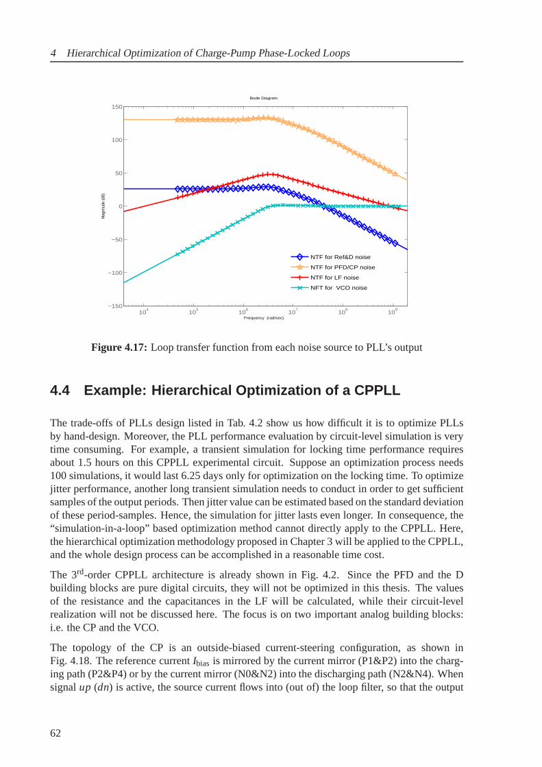
4 Hierarchical Optimization of Charge-Pump Phase-Locked Loops
104
105
106
107
108
109
−150
−100
−50
0
50
100
150M
agni
tude
(dB)
Bode Diagram
Frequency (rad/sec)
NTF for Ref&D noise
NTF for PFD/CP noise
NTF for LF noise
NFT for VCO noise
Figure 4.17: Loop transfer function from each noise source to PLL’s output
4.4 Example: Hierarchical Optimization of a CPPLL
The trade-offs of PLLs design listed in Tab. 4.2 show us how difficult it is to optimize PLLsby hand-design. Moreover, the PLL performance evaluation by circuit-level simulation is verytime consuming. For example, a transient simulation for locking time performance requiresabout 1.5 hours on this CPPLL experimental circuit. Supposean optimization process needs100 simulations, it would last 6.25 days only for optimization on the locking time. To optimizejitter performance, another long transient simulation needs to conduct in order to get sufficientsamples of the output periods. Then jitter value can be estimated based on the standard deviationof these period-samples. Hence, the simulation for jitter lasts even longer. In consequence, the“simulation-in-a-loop” based optimization method cannotdirectly apply to the CPPLL. Here,the hierarchical optimization methodology proposed in Chapter 3 will be applied to the CPPLL,and the whole design process can be accomplished in a reasonable time cost.
The 3rd-order CPPLL architecture is already shown in Fig. 4.2. Since the PFD and the Dbuilding blocks are pure digital circuits, they will not be optimized in this thesis. The valuesof the resistance and the capacitances in the LF will be calculated, while their circuit-levelrealization will not be discussed here. The focus is on two important analog building blocks:i.e. the CP and the VCO.
The topology of the CP is an outside-biased current-steering configuration, as shown inFig. 4.18. The reference currentIbias is mirrored by the current mirror (P1&P2) into the charg-ing path (P2&P4) or by the current mirror (N0&N2) into the discharging path (N2&N4). Whensignalup (dn) is active, the source current flows into (out of) the loop filter, so that the output
62

4.4 Example: Hierarchical Optimization of a CPPLL
voltage of the loop filter rises (drops), which forces a higher (lower) oscillation frequency con-sequently. Note that signalsup anddn cannot be active at the same time, which means the LFcannot be charged and discharged at the same time. Signalsup anddn are the complement ofthe signalsup anddn respectively. The dummy switches (N5&P6) are intended to avoid anyvoltage peak at the output node.
VSS
VDD
P1 P2
P3
N5
N1 N2
N3
N0
up
dn
P4
N4
up
Ibias
P6
up
Dummy switches
Iout
up
up
dn
dn
dn dn
Figure 4.18: Schematic of CP Block
The VCO is a five-stage single-end ring oscillator, as shown in Fig. 4.19. The input voltageVctrl controls the current through the delay elements, thus determines the delay time of eachstage and in turn determines the output oscillation frequency. The upper and lower transistors,e.g. P1&N1, act as the voltage control current sources (VCCS), and the middle transistors,e.g. P6&N6, act as the delay elements. The current flowing through these delay elements isgenerated by these current mirror structures, e.g. (N0&N1 and P0&P2).
4.4.1 CPPLL Hierarchical Modeling
In this experiment, the CPPLL is realized in a 180nm technology with a supply voltage VDDof 3V, using a reference signalfin of 25MHz to generate the output frequency ranging fromfmin (=150MHz) to fmax (=500 MHz). In the hierarchical modeling of the CPPLL, systemperformances are modeled in dependence of system-level parameters from each building block,while these system-level parameters can be determined by simulation of the blocks on circuitlevel. Fig. 4.20 gives an overview of the hierarchical performance modeling of the CPPLL.
63

4 Hierarchical Optimization of Charge-Pump Phase-Locked Loops
Vctrl
Vout
P1 P2 P3 P4 P5
P6 P7 P8 P9 P10
N6 N7 N8 N9 N10
N1 N2 N3 N4 N5N0
P0
VDD
VSS
Figure 4.19: Schematic of VCO Block
4.4.1.1 CPPLL on System Level
System-level performances Six important performances of the CPPLL system are consid-ered: locking time, jitter, power consumption, unity-gain bandwidth, phase margin and outputfrequency.
The locking time is defined as the time taken by the CPPLL to synchronize with or to lock onto anew frequency. The performance optimization shall be considered at the worst case. Thereforethe locking time is defined as the time for the output frequency directly jumping from fmin
(150MHz) to fmax (500MHz).
The total output noise of the CPPLL comes from the CP and the VCO in this experiment, whilethe input signal and other building blocks are considered asnoise-free. The CPPLL exhibitsvarious noise transfer characteristics with respect to thedifferent noise sources, as discussed inSec. 4.3.4. Hence, the design of the loop bandwidth has to be atrade-off for jitter of the VCOand jitter of the CP when minimizing the total output jitter.The jitter performance shall also beoptimized at its worst case, i.e. when the CPPLL works at its minimal output frequencyfmin
§.
With the predetermined digital building blocks PFD and divider, the power consumption isdefined as the sum of the power consumption in the CP and VCO (weconsider only analogblocks¶):
Power= VDD ·4 · ICP+VDD · IVCO. (4.32)
§ At the minimal output frequency, the current consumption isminimal (VCO current consumption is minimaland other blocks keep constant) so that the jitter performance is worst, which can also be seen from the Pareto-optimal front of the VCO in Sec. 4.4.3
¶ The current consumption of LF is not needed to calculate, since the charging or discharging currents in LF arefrom or to CP.
64

4.4 Example: Hierarchical Optimization of a CPPLL
We consider the worst-case power consumption that occurs when the CPPLL works at its max-imal output frequencyfmax.
For the optimization process, locking time, jitter and power consumption are taken as the opti-mization targets at the system level:
f = [Ts,Jsum,Power]T . (4.33)
The output frequency range of the CPPLL is determined by the VCO, therefore this perfor-mance is directly forwarded as a circuit-level performanceof the VCO block. Additionally, twoconstraints concerning stability are considered for system-level optimization:
• The stability criterion RUR for nonlinear acquisition process. We specify RUR≥ 20.
• The stability criterion PM for linear lock-in state. We specify PM ≥ 45
system-level parameters For each building block of the CPPLL, a set of system parametersp that are capable of capturing the influence of the blocks on the system performances & trade-offs, are defined:
• CP: outside-biased reference currentICP, jitter JCP
• VCO: gainKVCO, current consumptionIVCO, jitter JVCO
• LF: loop filter elementsR, C1, C2
• D: divider valueN ‖
4.4.1.2 CPPLL on Circuit Level
Circuit-level performances On circuit level, the system-level parameters become perfor-mances of the building blocks that can be simulated in dependence of circuit-level design para-meters. For the CP for instance, the absolute values of the simulated charging and dischargingcurrentsIup andIdown are equal to the value of the outside-biased currentICPon behavioral level,and the system-level jitterJCP becomes a circuit-level performance of the CP. For the VCO,gain, current consumption, jitter and output frequency range are the circuit-level performancescorresponding to the system-level parameters.
Circuit-level parameters The transistor dimensions, i.e. widths/lengths, are the circuit-levelparameters. In the CP in Fig. 4.18, there are two sets of current mirror structures, i.e. P1&P2and N0&N1&N2. The transistor dimensions in a current mirrorstructure should be identical. Inthe VCO in Fig. 4.19, there are also two current mirror structures, i.e. P0&P1&P2&P3&P4&P5and N0&N1&N2&N3&N4&N5. The dimensions of other transistors in both circuits are set assame as that of the digital circuit. Since the transistors inVCO block work in large-signalfunction, the sizing rules in Fig. 4.20 are only related to the geometric rules in Tab. A.2. Forthe current mirror transistors in CP block, the sizing rulesincludes not only geometric rules butelectrical sizing rules as well.
‖ The divider value is determined by the input and the expectedoutput frequency.
65

4 Hierarchical Optimization of Charge-Pump Phase-Locked Loops
CPPLL
Locking Time, Jitter, Power, RUR, PM, Output Frequency
CPPLL System
System performances
System-level parameters
PFD CP LF VCO D
ICP, JCP R, C1, C2 KVCO, IVCO, JVCO N
Building block
Circuit-level performances
Iup, Idown, JCP, sizing rules
KVCO, IVCO, JVCO, Output Frequency
Transistor dimensions
W/L
Transistor dimensions
W/L
Circuit-level parameters
sizing rules
Figure 4.20: Hierarchical performance modeling of the CPPLL
4.4.2 Modeling CPPLL in Verilog-A
Recently, various behavioral models [AETL96, SG99, HKH00,OHSA04, Kun05] have beendeveloped to accelerate the system-level simulation of PLLs. In this thesis, the system-levelmodels are based on [Kun05], which are realized in Verilog-A[Verb]. To achieve efficientmodeling and fast extraction, two sets of models are used forlocking time and jitter respectively.The first set of models, list D.1-list D.4 in Appendix D, focuses on more accurately representingthe nonlinear acquisition locking process, while the second set, list D.5-list D.8, focuses onmore efficient modeling of the jitter in order to accelerate jitter simulation.
Models for locking time extraction In order to more accurately model the nonlinear acqui-sition process, some properties of building blocks are included and presented as follows. Forexample, the rising/falling time, delay time of the PFD block are firstly extracted from circuitlevel simulation and then are parameterized astd_ul andtd_dl in the behavioral model.
module PFD (ref, feedback, u, ub ,db ,d);input ref, feedback;output u, ub, db,d;electrical ref, feedback, u, ub, db, d;......parameter real tt=120p from (0:1000000); //rise time and fall time// the following delay times are extracted from circuit level simulation// for "u" and "ub" signal:// ---------- rise delay ------------- fall delay
66

4.4 Example: Hierarchical Optimization of a CPPLL
parameter real td_u1=37p; parameter real td_u2=190p;// for "d" and "db" signal:parameter real td_d1=45p; parameter real td_d2=136p;......
endendmodule
Since the charging/discharging current sources in Fig.4.18 are realized by N/PMOS transistors,theses N/PMOS transistors will work out of saturation ranges if the output voltage goes too highor too low. Therefore the generated output current cannot bethe same value as the out-sidedbiased reference current. The two parametersV_maxandV_min in the CP model are used torepresent the limit of the output voltage. The parameterMis is used to represent the mismatchcurrent between the charging and the discharging currents.
module CP(Iout, Down, N_Down, N_Up, Up, Ibias);input Up, N_Up, Down, N_Down;output Iout;electrical Up, N_Up, Down, N_Down, Iout;......parameter real Ip=25.0e-6; //charge pump’s output currentparameter real v_max=2.85; //maximum voltage at output node
//so that PMOS current source in saturationparameter real v_min=0.35; //minimum voltage at output node
//so that NMOS current source in saturationparameter real Mis=0.00; //Mismatch of up and down current.....
analog begin.....// restrict the output voltage range from v_min to v_max@(cross(V(Iout)-v_max, 1)) begin
state =0end@(cross(V(Iout)-v_min, -1))begin
state =0;endI(Iout)<+transition(Ip*state*(1+state*Mis), Delay, TransTime );
endendmodule
In the VCO block, according to [LMC01], the linear VCO model predicts more than 90% of thereal VCO characteristics, especially in the operating range. In this experimental PLL’s VCO,when the input voltage is in the input range, the VCO output frequency increases with thelinear gainKVCO. When the input voltage exceeds the maximum input level, theVCO outputfrequency can still increase, but the gain is set to be 0.25KVCO instead ofKVCO.
module vco(V_tune,VCO_out);input V_tune;output VCO_out;electrical V_tune, VCO_out;......parameter real Vmin=0.6;
67

4 Hierarchical Optimization of Charge-Pump Phase-Locked Loops
parameter real Vmax=2.6 from(Vmin:10e5);parameter real Kvco=600e6;......
analog begin......// compute the freq from the input voltageif (V(V_tune)<=Vmin)
freq = Fmin;else if (V(V_tune)<=Vmax)
freq = (V(V_tune)-Vmin)*Kvco+Fmin;else
freq = (V(V_tune)-Vmax)*(0.25*Kvco)+(Vmax-Vmin)*Kvco+Fmin;......
endendmodule
Models for jitter extraction In a transient simulation, step size in simulation setup is acrucialfactor for time cost and simulation accuracy. If jitters of CP and of VCO cause two individualevents and the two events are displaced at almost same time points but not exactly coincident,then circuit simulators have to spend many more time points (i.e. smaller step size) to resolvethe two distinct events, hence the simulation will run much slower. For this reason, it is desirableto reduce the number of jitter events by combining jitter sources compactly. The jitter of CPblock, i.e. edge-to-edgeJCP, can be embedded into the model of the reference input oscillator(OSC) block. The following parametersyncJitterrepresents the jitter of CP.
module OSC(out);output out; electrical out;parameter real freq=25e6 from (0:10e9);parameter real accJitter=0 from [0:0.1/freq);
//period jitter from reference OSCparameter real syncJitter=0 from [0:0.1*ratio/freq);
//edge-to-edge jitter from PFD/CP......
endendmodule
As well known, the higher frequency the circuit runs at, the step size in simulation setup hasto be smaller. The output frequency of VCO isN times (divider value) of the internal signalfrequency of CPPLL. When divider and VCO are merged together, the simulation can run muchfaster because the high VCO output frequency is never generated actually. The acceleration ofsimulation is obvious. If divider is merged into the module of VCO, the period jitter at theVCO output should be
√N time larger than the period jitterJVCO [Kun05]. Since there are two
transient processes in one period: i.e. one rising edge and one falling edge, the output jitter ofthe VCO_Div block is therefore equal to
JVCO_Div =√
2NJVCO. (4.34)
The merged behavioral model for VCO with divider is named as VCO_Div. The Verilog-Amodel is given in the following.
68

4.4 Example: Hierarchical Optimization of a CPPLL
module VCO_Div(V_tune,VCO_out);input V_tune; output VCO_out;electrical V_tune, VCO_out;
......parameter real N=20; //if N!=1, divider moved into the VCO blockparameter real Jvco=10e-12; //Jitter of VCO......
analog begin@(initial_step)begin
seed=160;Vout=VSS;delta=Jvco*sqrt(2*N);// calculating the corresponding jitter on the divider output
end......
endmodule
Based on the above efficient setups in the behavioral models,the system-level simulations forthe locking time and the jitter can be finished in some minutes. The reasonable simulation timemakes the “simulation-in-a-loop”-based optimization methods feasible for PLL circuits.
4.4.3 Pareto-Optimal Fronts of Building Blocks
The deterministic PSE method mentioned in Chapter 3 is applied to the circuit level of the CPand the VCO respectively. The extracted Pareto fronts presented here are computed throughreal circuit-level simulation, which is a non-trivial task.
PSE on CP For the CP, small jitter and low power consumption are desired. Fig. 4.21 showsthe Pareto-optimal front for the outside-biased current and the output jitter of CP, which rep-resents the lower bound on the combination of both performance values. Right and above thefront is the feasible region. The trade-off front indicatesthat a larger current will result in asmaller jitter.
PSE on VCO Fig. 4.22 shows the feasible ranges bounded by the Pareto fronts for the com-peting objectives jitter, gain and current of the VCO in 3-D and in the different 2-D projections.We can evaluate e.g. the increasing trend ofJVCO with increasingKVCO for constantIVCOfrom Fig. 4.22(b), or howKVCO increases at the cost of a largerJVCO for constantIVCO fromFig. 4.22(c), or the increasing trend ofIVCO with the decreasing ofJVCO for constantKVCO fromFig. 4.22(d).
The feasible regions for system-level parameters, i.e.ICP,JCP, IVCO,KVCO andJVCO, can beextracted from the Pareto-optimal fronts in Fig. 4.21&4.22.
4.4.4 Hierarchical Optimization
Through restricting the system-level parameters on their own Pareto-optimal fronts, an optimalperformance of the whole circuit can be obtained [EMG05]. Inthis experiment, the independent
69

4 Hierarchical Optimization of Charge-Pump Phase-Locked Loops
0 0.5 1 1.5
x 10−4
0
0.5
1
1.5
2
2.5
3
x 10−11
ICP
J CP
Fitting CurveOrginal Data
Popt
Figure 4.21: Pareto-optimal front of the CP
system-level parameter set is selected asp =[ICP, IVCO,KVCO,R,C1,C2]. The parameterJCP isdependent on the parameterICP andJVCO is dependence on the parametersIVCO andKVCO, asexpressed in Equation 4.35. There are two ways to transfer the jitter values into the behavioralmodels. One way is to directly embed the fitting function intothe models given in List D.5 andList D.7. The other way is to calculate the jitter values through a special script file firstly; andthen to transfer these values to the jitter parameters of themodels by means of circuit netlistmapping:
JCP = fitting_function_1(ICP)
JVCO = fitting_function_2(IVCO,KVCO).(4.35)
4.4.4.1 File system in WiCkeD
In the thesis, the optimization process is realized in WiCkeD [Wic]. The file system for theCPPLL optimization is briefly listed in Fig. 4.23, and the setup for other optimization tasks inother parts of the thesis is similar to this. The file system can be classified into four levels.At the first level, “CPPLL.def” is the main file for optimization setup, including the followingfunctions:
• The parameters are defined, i.e. design parameters, statistical parameters and operationparameters. And their corresponding upper and lower boundary are also given.
• The circuit performances and the necessary optimization constraints are defined. And theircorresponding simulations are set, e.g. "LockingTime.rs"for locking time performance,"Jitter.rs" for jitter performance.
70

4.4 Example: Hierarchical Optimization of a CPPLL
010
20
020
40
0
5
10
15
(a)
Ivco
*1e−4KVCO
*1e8
J VC
O*1
e−12
2.383
7
2.3837
3.69
52
3.69
52
8.94
16IVCO
*1e−4
KV
CO
*1e8
(b)
0 5 10 150
5
10
15
20
11.0828
11.0828
16.7382
IVCO
*1e−4
J VC
O*1
e−12
(c)
0 5 10 150
5
10
2.65688
4.37464
11.245711.2457
KVCO
*1e8
J VC
O*1
e−12
(d)
0 5 10 15 200
2
4
6
8
10
12
14
Popt
Popt
Popt
Figure 4.22: Pareto-optimal front of the VCO
71

4 Hierarchical Optimization of Charge-Pump Phase-Locked Loops
FeasibleRegionChecking.m
PM.m
RUR.m
Power.m
Octave.rs
pll_ts.ocn
beh. model D.4
beh. model D.3
beh. model D.2
beh. model D.1
pll_ts.scs
LockingTime.rs
pll_jit.ocn
beh. model D.8
beh. model D.7
beh. model D.6
beh. model D.5
pll_jit.scs
Jitter.rs
CPPLL.def
Figure 4.23: File system in WiCkeD
• The simulation tasks are distributed to many machines simultaneously. The performancesand constraints can be extracted in parallel.
At the second level, “***.rs” is the setup file for the performances and constraints, which con-trols the simulation and extraction files at the third level.For example, “Jitter.rs” controls twofiles: “pll_jit.scs” is theSpectre-format netlist of the transient simulation for jitter performance,and “pll_jit.ocn” is in charge of the jitter extraction fromprimal simulation data bank. Thebehavior-level modules list D.5-list D.8 are included at the fourth level.
In the optimization of the CPPLL, one transient simulation with Spectreis used to obtain thelocking timeTs, while another transient simulation is for the jitterJSUM. Based ons-domainanalysis of the PLL, the linear lock-in state properties, e.g. unity-gain-bandwidth and phasemargin, are calculated. A third simulation with octave [Oct] is used for the system-level con-straints: the ratio RUR, the PM and the feasible ranges of thesystem-level parameters.
4.4.4.2 Hierarchical Optimization Results
Tab. 4.3 shows the results of the two optimization steps (top-down automatic sizing and bottom-up verification) in hierarchy. Starting from the system specifications in column 3 and the initialdesign in column 4, system-level optimization leads to the optimized system performances inthe upper half of column 5 and the system-level parameters inthe lower half of column 5. Thelatter, propagated as specifications to the circuit-level optimization, results in the finalPopt,
72

4.5 Pareto-Optimal Front Computation (POFC) of a whole CPPLL
which are listed in the lower half of the last column and depicted in dots in Fig. 4.21&4.22, re-spectively. A system simulation with the behavioral modelscalibrated according to the circuit-level design parameters yields the system performances in the upper half of column 6. We cansee that by considering the technological feasibility of building blocks a first-time-successfulhierarchical optimization has been achieved for a comprehensive set of design aspects. The op-timization on system level and circuit level requires about1.5 hours respectively, which resultsin a total of 3 hours.
4.5 Pareto-Optimal Front Computation (POFC) of a wholeCPPLL
Compared to only one optimization design point in the last experiment example, a comprehen-sive optimization result, i.e. Pareto-optimal front of thesystem performance, will be computedin this experiment example. PSE method is applied not only tothe building blocks but to thewhole CPPLL system as well. The trade-offs in the performance of building blocks, e.g. gain,jitter and power in VCO, and the performance at system level,e.g. bandwidth, locking time andjitter, will be represented as Pareto-optimal fronts. These fronts offer designers a fast way to getinsight into the capability of the whole system for a given technology.
The topologies of the building blocks in this experiment areexactly same as those of the lastexperiment. The technology is 130nm and the normal supply voltage VDD is 1.8 volt. Thereference input signal isfin=25MHz. The CPPLL is supposed to generate the output frequencyfout=500MHz.
4.5.1 POFC of the CP Block
For the CP block, the feasible range of the out-biased current is set from 5µA to 65µA. ThePareto-optimal front in Fig. 4.24 represents the trade-offrelationship between the two perfor-mances, that the output jitter of CP decreases with the increasing current. The front shows thelower bound for both performances, right and above the frontis the feasible region.
4.5.2 POFC of the VCO Block
For POFC on the VCO block, two constraints are set:
1. the maximal output frequency is larger than the expected output frequency, so that the VCOis capable of providing the 500MHz output frequency;
2. the nonlinearity limit of the gain is set to 2.5 to guarantee the acceptable linearity of VCO,i.e.
fmid− fmin
fmax− fmid≤ 2.5, (4.36)
where fmid is the corresponding output frequency of the input voltageVmid = (Vmax−Vmin)/2.
73

4 Hierarchical Optimization of Charge-Pump Phase-Locked Loops
12
34
56
System
Perfo
rman
cesS
pecificatio
ns
Initiald
esign
System
-levelC
ircuit-level
&b
locks
op
timizatio
no
ptim
ization
Lockin
gT
ime
Ts
(µs)
≤2
.52
.85
2.1
32
.2JitterJ
sump
s≤
2.5
20
.82
.25
2.2
1S
ystem:
Pow
er(m
W)
≤2
.53
.02
2.4
22
.41
7C
PP
LLR
atioR
UR
≥2
03
0.6
@fm
in2
8.5
@fm
in2
8.7
@fm
in
78
.6@
fmax
72
.8@
fmax
73
.5@
fmax
Ph
aseM
argin
PM
( )≥
45
43
.6@
fmin
45
.1@
fmin
45
.1@
fmin
48
.0@
fmax
45
.1@
fmax
45
.0@
fmax
Blo
ck:C
urren
tICP
(µA)
50
47
.3Iup =
46
.5Idow
n =-4
6.5
CP
JitterJC
P(p
s)5
5.2
13
.34
14
.4B
lock:
Gain
KV
CO
(MH
z/V)
27
0.3
34
7.1
34
8.4
VC
OC
urren
tIVC
O(µA
)8
05
.96
19
.26
19
JitterJV
CO
(ps)
13
.71
.88
1.8
76
Blo
ck:R
esistorR
(KΩ
)2
01
6.9
81
6.9
8LF
Cap
acitorsC
1 &C
2 (pF
)5
0&
84
4.5
&7
.66
44
.5&
7.6
6
Table4.3:H
ierarchicalo
ptim
ization
results
ofth
eC
PP
LL
74

4.5 Pareto-Optimal Front Computation (POFC) of a whole CPPLL
0 10 20 30 40 50 60 708
10
12
14
16
18
20
Current*1e−6
Jitte
r*1e
−12
Fitting curveOrginal data
Figure 4.24: Pareto-optimal front of the CP
Large gain, small jitter and low current consumption are preferred in the VCO block. The 3DPareto-optimal front for these three competing objectivesis shown in Fig. 4.25(a). The contoursof jitter on the Pareto front surface is shown in Fig. 4.25(b), which represents the jitter is reducedby increasing current consumption for a fixed gain.
1020
3040
0
2
40
5
10
IVCO
*1e−5KVCO
*1e9
2.02
96
3.5287
9.52
5
IVCO
*1e−5
KV
CO*1
e9
J VC
O*1
e−12
10 20 300.5
1
1.5
2
2.5
fitting curveorginal data
(a) (b)
Figure 4.25: (a) 3D Pareto-optimal front of the VCO (b) Contours of jitterin 2D surface (gainvs. current)
4.5.3 POFC of the CPPLL System
For POFC on CPPLL system level, three constraints are set:
75
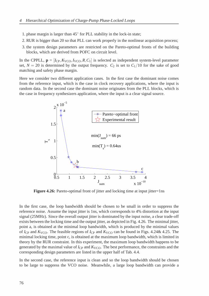
4 Hierarchical Optimization of Charge-Pump Phase-Locked Loops
1. phase margin is larger than 45 for PLL stability in the lock-in state;
2. RUR is bigger than 20 so that PLL can work properly in the nonlinear acquisition process;
3. the system design parameters are restricted on the Pareto-optimal fronts of the buildingblocks, which are derived from POFC on circuit level.
In the CPPLL,p = [ICP,KVCO, IVCO,R,C1] is selected as independent system-level parameterset,N = 20 is determined by the output frequency.C2 is set toC1/10 for the sake of goodmatching and safety phase margin.
Here we consider two different application cases. In the first case the dominant noise comesfrom the reference input, which is the case in clock recoveryapplications, where the input israndom data. In the second case the dominant noise originates from the PLL blocks, which isthe case in frequency synthesizers application, where the input is a clear signal source.
0.5 1 1.5 2 2.5 3 3.5 4
x 10−10
0
0.5
1
1.5
2x 10
−5
min(Jsum
) = 66 ps
min(T
s) = 0.64us
Jsum
Ts
a
b
c
Pareto−optimal frontExperimental result
Figure 4.26: Pareto-optimal front of jitter and locking time at input jitter=1ns
In the first case, the loop bandwidth should be chosen to be small in order to suppress thereference noise. Assume the input jitter is 1ns, which corresponds to 4% distortion at the inputsignal (25MHz). Since the overall output jitter is dominated by the input noise, a clear trade-offexists between the locking time and the output jitter, as depicted in Fig. 4.26. The minimal jitter,point a, is obtained at the minimal loop bandwidth, which is produced by the minimal valuesof ICP andKVCO. The feasible regions ofICP andKVCO can be found in Figs. 4.24& 4.25. Theminimal locking time, point c, is obtained at the maximum loop bandwidth, which is limited intheory by the RUR constraint. In this experiment, the maximum loop bandwidth happens to begenerated by the maximal value ofICP andKVCO. The best performance, the constraints and thecorresponding design parameters are listed in the upper half of Tab. 4.4.
In the second case, the reference input is clean and so the loop bandwidth should be chosento be large to suppress the VCO noise. Meanwhile, a large loopbandwidth can provide a
76

4.5 Pareto-Optimal Front Computation (POFC) of a whole CPPLL
0 0.2 0.4 0.6 0.8 1
x 10−11
0.5
1
1.5
2
2.5
x 10−6
Jsum
Ts
f
e
g
min(Jsum
) = 1.08ps
min(T
s) = 0.64us
Pareto−optimalfrontExperimental result
Figure 4.27: Pareto-optimal front of jitter and locking time at input jitter=0 and settingICP= Imax
quick acquisition process. At a first glance, it seems that there is no contradiction betweenreducing locking time and output jitter. From Sec. 2.3, the loop bandwidthωBW is increasedby increasingICP. When ICP reaches the maximum but theωBW is still not large enough, itcan be further enlarged by increasingKVCO. A largerKVCO introduces more VCO noise, whichresults in a larger output jitter. Fig. 4.27 shows the trade-off between the jitter and the lockingtime, where the input noise is 0ps and theICP is set to maximum. The relationship of theloop bandwidth at the points e, f, g is:ωe > ω f > ωg. This indicates that the output jitter isincreased much more by VCO noise than decreased by the enlarged loop bandwidth. Therefore,minimizing jitter is equivalent to minimizing VCO noise. The best performance, the constraintsand the corresponding design parameters are listed in the lower half of Tab. 4.4.
The ultimate sizing goal is to optimize locking time, jitterand power consumption simultane-ously. The performance and the corresponding system-levelparameter sets for the two differentcases introduced in Sec. 4.3 are collected in rows b and f in Tab. 4.4. These obtained valuesof the system-level parameters can be successfully realized by the final circuit level. Moreover,the two compromise optimization results, b and f, are also denoted by pentagrams in Fig. 4.26and Fig. 4.27 respectively.
It is worth noting one point here. Based on the discrete computed efficient points, an entirePareto-optimal front is estimated by means of a smooth fitting curve or surface in this work.Although the residual at certain efficient point∗∗ in the fitting function is not small sometimes,the highest-level optimization results based on the fittingPareto-optimal fronts can really re-alized by the final lowest-level circuit in the two optimization experiments. That proves again
∗∗ These efficient points might be generated due to non-robust algorithm of performance space exploration.
77

4 Hierarchical Optimization of Charge-Pump Phase-Locked Loops
that the behavior of a circuit is usually well-natured so long as it works in the correct region ofoperation.
4.6 Summary
This chapter has discussed the basic concept behind of the phase-locked loop. The buildingblocks and their operation of a charge pump phase-locked loop are briefly explained. Threeanalysis methods:s-domain analysis, impulse invariance method and state space method areused to characterize the system properties of CPPLL in linear lock-in state and nonlinear acqui-sition process.
The PLL’s performances, i.e. locking time, phase noise/jitter are discussed in detail. Addition-ally, the PLLs’ stability criteria for linear lock-in stateand for nonlinear acquisition process arediscussed individually. The design trade-offs among the loop bandwidth, locking time and jitterare analyzed in theory and visualized by the experimental results.
In this work, to tackle the complex trade-offs in the PLL design, we present an optimizationmethod to find a proper loop bandwidth in order to optimize performance in terms of lockingtime and jitter, which considers the capability of the building blocks. The experimental re-sults are consistent with the theoretical analysis. The Pareto-front computation on system levelprovides a comprehensive insight into the circuit’s capability. In clock recovery or frequencysynthesizer applications, starting from various requirements on the PLL’s loop bandwidth to fi-nal circuit realization, the automatic sizing process can be accomplished in hours. Moreover, itis a first-time-successful top-down sizing process withoutiteration. Without the proposed hier-archical approach, a complete CPPLL design could need many iteration steps due to complexityproblems.
78

4.6 Summary
Jitt
erLo
ckin
gT
ime
Pow
erR
UR
PM
VC
OC
PLF
J sum
(ps)
T s(µs)(µ
w)
Cas
e1:
Inpu
tJitt
er=
1ns
a3
86
0.6
46
42
20
45
KV
CO
=2
.2e9
Hz/
VI C
P=6
5µAC1=
27
.2p
FI V
CO
=1
61
.5
µAJ VCO=8.41
ps
J CP=
8.2
1p
sC
2=2
.72
pFR
=5
.9k
b1
24
.12
.64
20
97
54
6.4
KV
CO
=1
.53
7e9
Hz/
VI C
P=
11
.3
µAC1=
48
pF
I VC
O=
82
.41µAJ VCO=5.
6p
sJ C
P=1
5.7
4p
sC
2=2
.72
pFR
=1
3.4
kc
66
.41
9.0
22
79
24
44
5K
VC
O=
57
3.6
e6H
z/V
I CP=
5µAC
1=
80
pF
I VC
O=
14
0.2
µAJ VCO=1.04
8p
sJ C
P=1
8.8
7p
sC
2=
8p
FR
=2
4.5
k
Cas
e2:
Inpu
tJitt
er=
0e
9.6
70
.64
65
22
04
5K
VC
O=
2.2
e9H
z/V
I CP=
65µAC
1=2
7.2
pF
I VC
O=
16
7µAJ VCO=7.9
3p
sJ C
P=8
.21
ps
C2=
2.7
2p
FR=
5.9
kf
2.5
80
.72
66
22
3.4
46.
6K
VC
O=
1.4
14
e9H
z/V
I CP=
65µA
C1=
23
pF
I VC
O=
17
3µAJ VCO=2.2
8p
sJ C
P=8
.21
ps
C2=
2.3
pF
R=
7.9
8k
g1
.08
2.5
66
69
50
.25
6K
VC
O=
57
3.6
e6H
z/V
I CP=
65µA
C1=
80
pF
I VC
O=
17
5µAJ VCO=1.0
2p
sJ C
P=8
.21
ps
C2=
8p
FR
=1
1.3
k
Tabl
e4.
4:H
iera
rch
ical
op
timiz
atio
nre
sults
attw
od
iffer
entc
ases
79


Chapter 5
Hierarchical Optimization ofSwitched-Capacitor Sigma-DeltaModulators
Data modulator is an indispensable circuit in nowadays chip, it converts analog signalx(t) intime-continuous domain to digital signalx(n) in discrete-time domain or converts the signal inthe reverse process. In last decades, oversampling data converters become more popular for highresolution medium-to-low-speed applications such as high-quality digital audio. "Oversamplingis the process of sampling a signal with a sampling frequencysignificantly higher than twice thebandwidth or highest frequency of the signal being sampled"[wik]. The major advantages ofoversampling method compared to other converter architectures are that high-selectivity analogfilters are not needed and the conversion properties are muchless sensitive to the circuitryimperfections and noisy environment.
Switch capacitor (SC) sigma-delta (Σ∆) modulator is an effective topology for high resolutionAnalog-to-Digital (A/D) conversion. SCΣ∆ modulators use not only the oversampling methodbut the noise shaping method as well. Hence, SCΣ∆ modulators inherit the oversampling’s ad-vantages, such as high tolerance to circuitry non-idealities and reduced accuracy requirementson sample-and-hold circuit. Despite such predominant properties of SCΣ∆ modulators, "it isstill governed by the limitations of its analog building blocks. In particular, it is sensitive tocircuit non-idealities at the input stage where no noise shaping has yet taken place" [TMG02].To extract the effects of the non-idealities of analog blocks on the circuit performance, a circuit-level simulation is the direct way generally. However the circuit-level simulation of SCΣ∆modulators is a huge time-consuming and large memory-capacity required process, which re-sults in that it is unfeasible on such circuit by directly using the "simulation-in-a-loop" basedoptimization approaches stated in [WRSVT88,AEGP00,HBL01,PKR+00,dPDL+01]. A hier-archical process is needed for optimization on SCΣ∆ modulators.
In this chapter, Sec. 5.1 introduces the fundamentals ofΣ∆ oversampling modulators. Sec. 5.2reviews the topology of a second-order SCΣ∆ modulator and lists out the major non-idealitiesof the building blocks. Sec. 5.4 shows the proposed hierarchical optimization method applied tothe second-order SCΣ∆ modulator. The SNR performance is maximized at the nominal designcase and at the worst design case respectively. Finally, Sec. 5.5 concludes.
81

5 Hierarchical Optimization of Switched-Capacitor Sigma-Delta Modulators
5.1 Σ∆ Oversampling A/D Converters
In this section, the basic topology of conventional converters and ofΣ∆ oversampling A/Dconverters are briefly described as follows. More details can be found in [FM98, Par]. Aconventional Nyquist A/D converter consists mainly of three blocks, as shown in Fig. 5.1(a.1):
• Anti-aliasing filter: It is a low-pass filter and prevents the input signals above Nyquistfrequency to bring new components in the base-band, which don’t belong to the originalsignal.
• Sample-hold circuit: By using a sampling signal with frequencyfs1, the sample-hold cir-cuit samples a continuously changing input signal each 1/ fs1 time interval and provides aconstant signal for the subsequent quantization process. If the sampled signal has afb fre-quency in Nyquist converters, the sampling frequency has tobe twice times offb in orderto avoid any aliasing, i.e. Nyquist frequencyfs1 = 2 · fb.
• Multi-level quantizer: The sampled analog signals are compared with the predefinedrefer-ence levels, and then the comparison results will be digitalized as the output signals.
In a N-bit Nyquist converter, the number of the quantization level is 2N and the number of thelevel interval is 2N −1. The interval valueq between two successive levels is referred to asleast-significant-bit (LSB) of the converter:
q =1
2N −1. (5.1)
This conversion has a quantization error up to±q/2 with same probability and the quantiza-tion noise power is equally spread over the entire signal bandwidth. Assumed the above threebuilding blocks are ideal, a perfect classicalN-bit Nyquist A/D converter has quantization noisepower spectral density ofq/(
√12· fs1) uniformly distributed within the signal bandwidth. The
noise spectrum is presented only at one side here, as shown inFig. 5.1(a.2). Thesignal-to-noiseratio (SNR)∗ performance of an idealN-bit Nyquist converter is [Bak04]
SNRideal = (6.02N+1.76) dB. (5.2)
However the A/D conversion is not ideal in practice. For example, the undesired signal abovethe Nyquist frequency cannot be attenuated enough to below the noise floor by the anti-aliasingfilter, or the output of the sample-and-hold circuit varies during the quantization process. Con-sequently, the quantization noise will be larger than its theoretical minimum value, then itseffective resolution will be less thanN-bit. The actual resolution, i.e.Effective Number of Bits(ENOB) is defined by
ENOB=SNR−1.76dB
6.02dB. (5.3)
In oder to achieve high-resolution by Nyquist converter, high performances for each buildingblock are required.
In oversampling converters, a much higher sampling ratefs2 (=R·2 fb) is applied in sample-hold circuit. The factorR is generally referred to asoversampling ratio(OSR). By the price of
∗ SNR is defined as the ratio between the signal power and the noise power: SNR= Psignal/Pnoise. SNR includesall noise sources, both thermal and quantization.
82

5.1 Σ∆ Oversampling A/D Converters
D/A
Ant
i-alia
sing
fil
ter
Mo
dula
tor
Dec
imat
or
Dig
ital f
ilter
Do
wn-
sam
plin
g
f b
(c.2
) N
ois
e sp
ectr
um o
f sig
ma
del
ta c
onve
rter
f s2/2
In
-ban
d no
ise
Rem
oved
noi
se
(a.1
) B
lock
dia
gram
of N
yqui
st A
/D c
onve
rter
x(t)
An
ti-al
iasi
ng
filte
r
f s1
x(n)
Mu
lti-le
vel
quan
tizer
Sam
ple
-hol
d ci
rcui
t
Qua
ntiz
atio
n no
ise
leve
l=
f b
112
s
q
f⋅
f s1=
2·f
b
f
N(f
)
(a.2
) N
oise
sp
ectr
um
of N
yqui
st c
onv
erte
r
f
N(f
)x(
t)x(
n)
(c.1
) B
lock
dia
gram
of s
igm
a de
lta A
/D c
onv
erte
r
Ant
i-al
iasi
ng
filte
rD
ecim
ator
Dig
ital f
ilter
Dow
n-sa
mpl
ing
x(t)
x(n)
(b.1
) B
lock
dia
gra
m o
f ove
rsam
plin
g A
/D c
onve
rter
f s2
Sam
ple
-ho
ld
circ
uit
f b f s
2/2
Dig
ital f
ilter
f
N(f
)
(b.2
) N
oise
spe
ctru
m o
f ove
rsam
plin
g co
nver
ter
Noi
se s
hapi
ng
Mu
lti-le
vel
quan
tizer
f s2=
R·2
f b
f s2=
R·2
f b
qua
ntiz
erin
teg
rato
r
Figure 5.1: Block diagram of A/D Converters and Noise spectrum
83
5 Hierarchical Optimization of Switched-Capacitor Sigma-Delta Modulators
high sampling rate at the input signal, oversampling methodbrings two benefits. One is thatthe requirement of anti-aliasing filter in oversampling converter is much more lower than that inNyquist converter. A simple passive first-order filter suffices mostly. The another benefit is thata high resolution A/D conversion is accomplished with a low-bit A/D converter. Assumed a fullprecision quantizer, the total noise power of oversamplingconverter is same as that of Nyquistconverter. However, the quantization noise is distributedover a wider bandwidth tofs2/2, i.e.R· fb (this phenomenon is normally callednoise averaging), as shown in Fig. 5.1(b.2). If adigital low-pass filter (LPF) is added at the output, then most part of the quantization noise canbe removed, moreover the wanted in-band signal is not affected. Through the noise averaging,the power of quantization noise in the bandwidth of interestis decreased by factorR. The idealSNR using oversampling method is calculated by [Bak04]
SNRideal = (6.02N+1.76+10logR) dB. (5.4)
If OSR is 2, then SNRideal can be increased by 3dB or the ENOB can be improved by 0.5 bits.In oversampling converters, decimator is needed besides the three blocks mentioned above, asshown in Fig. 5.1(b.1).
• Decimator: It filters all the signal components out of the signal band, which includes a bigpart of the quantization error power. The filtered signal is downsampled to the Nyquist ratewithout degrading SNR performance. The collective operation of the low-pass filtering andthe downsampling is known as decimation, which can be realized by purely digital circuit.
If only using oversampling method to increaseN-bit resolution more, the sample rate has tobe faster by a factor of 22N. TheΣ∆ converter does not need such a high oversampling ratiobecause the operation of modulator (in Fig. 5.1(c.1)) not only reduces the quantization noisepower within the signal band, but also pushes quantization noise power from the signal bandto outside of the signal band (this phenomenon is normally called noise shaping), as shownin Fig. 5.1(c.2). Consequently, the ideal SNR by oversampling plus one-order noise shapingprocess is [Bak04]
SNRideal = (6.02N+1.76−5.17+30logR) dB. (5.5)
The details of the noise shaping process in modulator will bediscussed in Sec. 5.3.
• Modulator: In this block the signal is over-sampled and quantized. Same as oversamplingconverter, it spreads the whole quantization noise power (afixed value) over the frequencyrange with bandwidth ofR· fb in order to reduce the quantization noise power within thesignal band. Furthermore, the modulator attenuates the quantization noise within the signalband and amplifies it outside the signal band by means of noiseshaping process. In conse-quence, most of the noise power lies out of the signal band. These out-of-band quantizationnoise could be filtered by decimator later.
Through noise averaging and noise shaping methods, the requirements on some building blocksare quite low inΣ∆ A/D converter. The anti-aliasing filter can be realized by a simple RC low-pass filter. The decimator is a pure digital block and can be designed with the help of matureCAD tools. In contrast, the modulator is in charge of the simultaneous implementation of thenoise averaging and the noise shaping. The enclosed intrinsic errors of modulator, e.g. inherentquantization errors and imperfections (non-idealities) of circuit performances, will degrade the
84

5.2 Second-Order Switched-Capacitor Sigma-Delta Modulators
converter performance [FAB99]. Therefore, the modulator block is taken as the to be optimizedcircuit in this work.
A large amount ofΣ∆ modulator architectures have been developed since 1980s. Tab. 5.1[FAB99] summarize the respective advantages and disadvantages of the most usedΣ∆ modula-tor architectures. Based on system stability, oversampling ratio, circuit complexity and circuitsensitivity, second-orderΣ∆ modulators are most selected architectures for high-resolution ap-plication. Their effectiveness has already been illustrated in a variety of applications, such asdigital speech processing systems and voice-band telecommunication in [KHE+86,BW88].
Advantages Disadvantages
Single-loop,1-bit low-order[LNGB88]
⋆ guaranteed stability
⋆ simple circuitry
⋆ maximum useful input range
need of high OSR
presence of noise patterns
Single-loop,1-bit high-order[AP87]
⋆ large SNR by using lowOSR
⋆ smaller noise pattern
potential instability
useful input range smallerthan full-scale range
need of low gain integrators
high-ordercascade[HIUK86]
⋆ guaranteed stability
⋆ large SNR by using lowOSR
⋆ maximum useful input range
sensitivity to circuit imper-fections
larger complexity of the dig-ital part
Multi-bit[CSC97]
⋆ better stability
⋆ large SNR by using lowOSR
⋆ smaller noise patterns
more complex digital andanalog circuitry
sensitivity to multi-bit DACnonlinearity
Table 5.1: Summary ofΣ∆ modulator architectures based on [FAB99]
5.2 Second-Order Switched-Capacitor Sigma-DeltaModulators
TheΣ∆ modulator can be implemented as a discrete-time system (switched-capacitor, switchedOP AMP) [BW88, GSS00] or as a continuous-time one (active RC or transconductor-C) [SZ96, CS00]. Compared to the continuous-time realization, the implementation usingswitched-capacitor circuit is compatible with standard CMOS process and is insensitive to clock
85

5 Hierarchical Optimization of Switched-Capacitor Sigma-Delta Modulators
jitter. Moreover, the frequency response of the noise shaping filter can be accurately set by therelative capacitor ratios. For this reason, a second-orderSC Σ∆ modulators is taken in thisthesis.
5.2.1 Building Blocks of a second-order SC Σ∆ Modulator
A topology of the second-order SCΣ∆ modulator [BW88] is shown in Fig. 5.2, consisting oftwo switched-capacitor integrators, a comparator and a 1-bit D/A converter.
s1 s3
s2
IN
Cs
Cf
s1
s4s2 Cs
Cf
Out
1bit DAC
s3
s4
Figure 5.2: A second-order SCΣ∆ modulator [BW88]
5.2.1.1 Switched-Capacitor Integrators
The two switched-capacitor integrators in Fig. 5.2 are identical. Each consists of an operationamplifier (OP AMP), a sampling capacitorCs and an integrating capacitorCf. Compared to astandard RC integrator, switched-capacitor (SC) integrator has two major advantages:
• Much reduced area to realize the same functionality: as seenin Fig. 5.3, a resistor is re-placed by the sampling/integrating capacitors and the periodical turn-on/off switches. Fora same time constant (τ = ReqCf ), a meg-ohm resistance can be replaced by a pico-faradMOS capacitance with a proper sampling rate.
• More stable time constant: the time constant of the RC integrator is closely related to theabsolute values of the resistance and the capacitance, while the time constant of the SCintegrator is determined by the relative ratio of the capacitances. The absolute values ofresistance and capacitance can vary±20∼ 30% in silicon realization. In contrast, capac-itances can superiorly match with each other, its relative ratio is much more constant thanits absolute values. Hence, the time constant is insensitive to the variations of process andof temperature.
In this experiment, the ratio ofCs/Cf is set as Equation 5.6 in oder to realize the gain of 0.5, i.e.
b =Cs
Cf= 0.5. (5.6)
A SC integrator has two operation phases, which are controlled by two non-overlapping clocks.The switches are closed when the controlling clocks are highand vice versa. The corresponding
86

5.2 Second-Order Switched-Capacitor Sigma-Delta Modulators
time diagram for all switches in the modulator is shown in Fig. 5.3. Duringφ1, switchess1&s3
are closed whiles2&s4 are open, and the capacitorCs of the integrator is charged by the inputVin. During φ2, switchess2&s4 are closed whiles1&s3 are open, the charge stored onCs istransferred toCf. Switchess1&s2 are closed after a little delay∆t of switchess3&s4 respectivelyin order to avoid charge injection onCs.
1
2
Cs
Cf
2
1
Vin
Vout
Ts
Req=Ts/Cs
s1&s3
t
t
s2&s41
2
Figure 5.3: Single-ended SC Integrator
The SC integrator is a key building block inΣ∆ modulators. Its non-idealities, e.g. switch ther-mal noise, finite DC gain and slew rate of OP AMP, have strong impact on the SNR performanceof Σ∆ modulators. We will discuss that in detail in Sec. 5.3.1.3.
5.2.1.2 Comparator
A comparator is used to quantize an analog signal in the loop.The generated digital outputwill be directly taken as the output signal and be fed back to the D/A converter at the sametime. As shown in Fig. 5.2, the comparator lies after the integrator block, its non-idealities areshaped by the loop in the same way that quantization noise is shaped. Therefore, the impact ofthe comparator’s non-idealities can be ignored. Generally, "a simple regenerative latch withoutpre-amplification or offset cancellation fulfills the comparator requirements" [BW88].
5.2.1.3 1-bit D/A Converter
The D/A converter transforms the digital output signal backinto an analog form, which acts asanother input of the modulator in addition to the reference input signal. Any D/A conversionerror will result in distortion at the modulator’s output. Since the conversion error is not attenu-ated, the DAC’s non-linearity conversion will considerably hurt the performance of modulators.
87

5 Hierarchical Optimization of Switched-Capacitor Sigma-Delta Modulators
In order to minimize the impact of non-idealities D/A converter on theΣ∆ modulators, 1-bitD/A converter is selected here. The advantage of an 1-bit D/Aconverter is that it is inherentlylinear and guarantees the D/A conversion from differentialnonlinearity, because there are onlytwo output values and only one step size.
5.3 Analysis on Σ∆ modulator in z-domain
In principle, quantization process is an intrinsic non-linear procedure, so aΣ∆ modulator isalso an inherently non-linear system. To analyze the behavior of a Σ∆ modulator, it can stillbe implemented by a linear operation if the quantization error is assumed to be additive whitenoise by fulfilling the following four conditions [Mal02]:
I. "All quantization levels are exercised with equal probability.
II. The quantization steps are uniform.
III. The quantization error is not correlated with the inputsignal.
IV. A large number of quantization levels are used".A general linear model for a modulator is shown in Fig. 5.4. Itis a two-input (x(n)& e(n)) and one-output (y(n)) system, whosez-domain expression is represented by
Y(z) = STF(z)X(z)+NTF(z)E(z)
=H(z)
1+H(z)X(z)+
11+H(z)
E(z),(5.7)
whereX(z) and E(z) presents the input signal and the quantization noise respectively; andSTF(z) andNTF(z) are the respectivez-domain transfer functions of the input and the quanti-zation noise.
H(z)
E(z)
X(z) Y(z)
Figure 5.4: Linear model of the modulator with an injected quantizationnoise
For the 2nd-order SCΣ∆ modulator topology in Fig. 5.2, the corresponding linear model isshown in Fig. 5.5. The ideal integrator’sz-domain transfer function including the necessaryclosed loop gain are given byH1,2(z), i.e.
H1(z) = H2(z) = 0.5z−1
1−z−1 . (5.8) Although only one-level quantization is used in the second-order SCΣ∆ modulator, the quantization error isstill assumed to be white noise, since the quantization noise will be firstly sharpened.
88

5.3 Analysis onΣ∆ modulator inz-domain
Thus, the ideal signal transfer function is given by
STF(z) =H1H2
1+H1H2+H2=
0.25z2−1.5z+0.75
. (5.9)
Whereas, the noise transfer function is to be
NTF(z) =1
1+H1H2+H2=
z2−2z+1z2−1.5z+0.75
. (5.10)
H1(z) H2(z)
E(z)
Y(z)X(z)
Figure 5.5: Ideal linear Model of the 2nd-order SCΣ∆ modulator
As can be seen, theSTF(z) in Equation 5.9 is a low-pass function, whileNTF(z) in Equa-tion 5.10 is a high-pass function. Therefore, the 2nd-order SCΣ∆ modulator can suppress thequantization noise in the signal band and will not attenuatethe input signal.
Fig. 5.6 shows the power spectral density (PSD) of an ideal 2nd-order SCΣ∆ modulator whenthe OSR is set to 256. As seen in this figure, the PSD of noise power is attenuated in the signal
103
104
105
106
−200
−150
−100
−50
0
Frequency [Hz]
PS
D [d
B]
SNR = 101.5dB @ OSR=256
ENOB = 16.56 bits @ OSR=256
Figure 5.6: PSD plot of the ideal 2nd-order SCΣ∆ modulator @ OSR=256:
89

5 Hierarchical Optimization of Switched-Capacitor Sigma-Delta Modulators
50 100 150 200 250 30060
70
80
90
100
110
OSR
SN
R (
dB)
Figure 5.7: SNR vs. OSR in the ideal 2nd-order SCΣ∆ modulator
band and is amplified outside the signal band. With 256 oversampling ratio, we can obtainthe maximal SNR is 101.5dB and the corresponding ENOB is 16.56bit. The higher OSR is,the lower PSD quantization noise is in the signal band. Consequently, SNR increases with theincreasing OSR as shown in Fig. 5.7.
5.3.1 Effects of Non-idealities
Sole quantization noise is taken into account in the ideal linear model ofΣ∆ modulator in the lastsection. AlthoughΣ∆ modulator is usually well-known for its robustness to the non-idealities ofthe building block compared to other data conversion architectures [CT92], it is still necessaryto take into account such non-idealities of the electrical implementations and the correspondingintroduced conversion error. Actually, the impact associated with such imperfections increaseswhen the modulator specifications are highly demanded because they become the dominanterror sources [BKMA88,DLM92]. The detailed analysis on thenon-idealities of building blocksare described in [BW88, FAB99]. Here, the effects of non-idealities on the SNR performanceare presented and the corresponding modeling of these non-idealities are built. The main non-idealities of SCΣ∆ modulators [BFM+99, MBF+03] can be classified into three categories,shown as follows:
• clock jitter
• integrator noise– switches thermal noise
– OP AMP noise
• integrator non-idealities
90

5.3 Analysis onΣ∆ modulator inz-domain
x(t)
A
1/(2*f in)
x(t+)
Figure 5.8: Clock jitter on sampling input signal
– DC gain
– bandwidth
– slew rate
– saturation (output range)
5.3.1.1 Clock Jitter
In SC Σ∆ modulators, the property of SC circuits is closely dependent on the charge transferprocess during each clock phase. As seen in Fig. 5.3, the fourclock signals are used to triggerthe switches in order to sample the input analog signal. Due to the clock jitters on the four clocksignals, a non-uniform sampling time sequence is applied onthe input signal, which results innonlinear distortions of the sampled signal. In consequence, the noise floor or the total harmonicdistortion of modulator is increased.
The distortion of the sampled signal is a function related tothe statistical property of the clockjitter and the modulator input signal. If the input signal isa sinusoidal signalx(t) with amplitudeA and frequencyfin, the distortion introduced by a sampling with an instant clock jitter (δ) is
x(t +δ)−x(t) =ddt
x(t)δ ≈ 2π finAcos(2π fint)δ. (5.11)
Fig. 5.8 illustrates the relationship between distortion and clock jitter. Since clock jitter isassumed as white noise in this thesis, so the oversampling process is helpful to reduce the signaldistortion introduced by the clock jitter. The total power of the distortion is(2π finδτA)2/2 anduniformly distributed from 0 tofs/2 [BW88].
Fig. 5.9 shows the PSD of the 2nd-order SCΣ∆ modulator with the clock jitter when the OSRis set to 256. The SNR performance is reduced from 101.5dB (only considering the inher-ent quantization noise) to 99.95dB (considering additional clock jitter with standard deviation∆τ = 4e−9). This effect can be simulated with SIMULINK by using the model in Fig. B.1 inAppendix B, which represents Equation 5.11.
5.3.1.2 Noise Sources
In the real circuit implementation ofΣ∆ modulators, the signal is corrupted not only by theintrinsic quantization noise, but by various electrical noises in the building blocks as well. A
91

5 Hierarchical Optimization of Switched-Capacitor Sigma-Delta Modulators
103
104
105
106
−200
−150
−100
−50
0
Frequency [Hz]
PS
D [d
B]
with clock jitterideal
SNR =101.5dB
SNR =99.95dB
Figure 5.9: Effect of clock jitter
typical switched-capacitor integrator is already shown inFig. 5.3. The most important noisesources affecting the operation of the SC integrator are thermal noise associated with the sam-pling switches and the intrinsic noise of the operational amplifier [MBF+03].
Switch Thermal NoiseSwitches in SC integrators are implemented with CMOS transistors. When a switch is on, theCMOS transistor works in triode region and has a finite on-resistance that introduces thermalnoise. Thermal noise is an electronic noise generated by thethermal agitation of the chargecarriers (usually the electrons) and usually presents in equilibrium. Thermal noise has a whitespectrum and wide band, is limited only by the time constant of the switched capacitors or thebandwidth of the OP AMP [MBF+03].
vn1 Cs
(a)
r1
vn3
r3
vn4Cs
(b)
r4
vn2
r2
Figure 5.10: Equivalent SC circuits in (a)φ1 (b) φ2
Referring to the SC integrator shown in Fig. 5.3, the sampling capacitorCs is in series withswitches, that periodically open and close with finite resistance. The equivalent circuit is shownin Fig. 5.10. r1, r2, r3 andr4 are the on-resistances of switchess1,s2,s3 ands4, respectively.vn1, vn2 vn3 andvn4 are white Gaussian noise sources, which modulate the thermal noise ofr1,
92

5.3 Analysis onΣ∆ modulator inz-domain
103
104
105
106
−200
−180
−160
−140
−120
−100
−80
−60
−40
−20
0
Frequency [Hz]
PS
D [d
B]
ideal
with switch thermal noise
with Op Amp noise
SNR=101.5dB
SNR=100.3dB
SNR=97.5dB
Figure 5.11: Effect of noise
r2, r3 andr4, respectively. Thus noise sources are sampled periodically ontoCs. The equivalentcircuit is a simple RC circuit at both phasesφ1 andφ2. Therefore, the total noise power can beevaluated by [NST97]
e2T =
Z ∞
0
4kTRon
1+(2πRonCs)2d f =kTCs
, (5.12)
wherek is the Boltzmann’s constant,T is the absolute temperature, and 4kTRon is the noisePSD associated with the switch on-resistance. The corresponding model for switch thermalnoise in simulink is shown in Fig. B.2.
Operational Amplifier NoiseThe intrinsic noise of operational amplifier includes thermal noise, flicker (1/f) noise, shot noiseetc. For these purely random noises, it is very hard to predict their instantaneous values at anytime. The usual method to calculate random noise is the average mean-square value of the noise.When having multiple noise sources in a circuit, all noises can be represented together by a totalroot mean square (rms) noise source, which is the square rootof the sum of the average mean-square values of each individual source. In the behavioral model of OP AMP, an input-referrednoise source with rms noise voltageVn is used to present the intrinsic noises in OP AMP:
y(t) = b · [x(t)+nopamp(t)], (5.13)
wherenopamp= Vn ·RN(t). (5.14)
b is the integrator gain, andRN(t) is a Gaussian random number with zero mean and unitystandard deviation. In this experiment, only thermal noiseis considered, while other noises areneglected. The corresponding model for thermal noise is shown in Fig. B.3.
93

5 Hierarchical Optimization of Switched-Capacitor Sigma-Delta Modulators
Fig. 5.11 shows the PSD of the 2nd-order SCΣ∆ modulator with the switch thermal noise andthe operation amplifier noise respectively, when the OSR is set to 256.
5.3.1.3 Operational Amplifier Non-idealities
In Sec. 5.3, the transfer functions of input signal and quantization noise (STF(Z) andNTF(Z),respectively) are based on an ideal integration process. Inpractice, the real behavior of anintegrator deviates from this ideal behavior due to severalnon-idealities of the analog circuitimplementation. The non-ideal effect of the integrator is aconsequence of the OP AMP’s non-idealities. Such as finite DC gain and bandwidth, slew rate and limited voltage region will resultin an incomplete transfer of charge in SC integrators. Thesenon-idealities will be discussedseparately in the following.
DC Gain To simplify analysis here, the effect of an infinite DC gain ofOP AMP in a first-orderΣ∆ modulator are formulated here, and the following equationscan be extended to thehigher-oder modulators. The transfer function of an ideal integrator with unity coefficient is
Hideal(z) =z−1
1−z−1 . (5.15)
For a first-orderΣ∆ modulator, the idealz-domain transforms of the input signal and the quan-tization noise are expressed as
Y(z) = STFideal(z)X(z)+NTFideal(z)E(z)
=Hideal(z)
1+Hideal(z)X(z)+
11+Hideal(z)
E(z)
= z−1X(z)+(1−z−1)E(z),
(5.16)
where|STFideal(z)| = 1|NTFideal(z)| → 0
for z→ 1 i.e. f → 0. (5.17)
As we can see from Equation 5.16, the output of the modulator is the delayed input signal plusthe in-band shaped quantization noise. In practice, a real integrator built by an OP AMP with afinite DC gainA0 provides a real transfer function:
Hreal(z) =z−1
1− (1−α)z−1 with α =1A0
. (5.18)
Therefore, the realz-domain transforms of the input signal and the quantizationnoise can beexpressed as
Y(z) = STFreal(z)X(z)+NTFreal(z)E(z)
=Hreal(z)
1+Hreal(z)X(z)+
11+Hreal(z)
E(z)
=z−1
1+αz−1X(z)+1+(1−α)z−1
1+αz−1 E(z),
(5.19)
94

5.3 Analysis onΣ∆ modulator inz-domain
Cs
Cf
2
Vs
Vout
Ts
tnTs-Ts/2
Vout
nTs
Vin(nTs-Ts)t0
SR
Figure 5.12: Integrator output response
where
|STFreal(z)|= | 11+α | ∼= 1−α
|NTFreal(z)| = |1+(1−α)z−1
1+α | ∼= |(1−α)(1−z−1)+αz−1| → αfor α ≪ 1 & z→ 1.
(5.20)An OP AMP with a finite DC gain affects the integration processby two aspects. Based onthe comparison between|STFideal(z)| and |STFreal(z)|, only a (1−α) fraction of the previousoutput of the integrator is added to the new input sample every time. This phenomenon is usuallyreferred as "leaky integration". Based on the comparison between|NTFideal(z)| and|NTFreal(z)|,quantization noise in the signal band is weakly attenuated.Hence the SNR performance isconsequently degraded by the incomplete integration process.
Bandwidth and Slew Rate Besides the finite DC gain of OP AMP, a finite bandwidth ora finite slew rate could also produce an inaccurate charge transfer within each clock cycle,which leads a non-ideal transient response in SC circuits. The effect of the imperfections onbandwidth and slew rate are correlated to each other and can be interpreted as a nonlinear gain[MPVARVH94].
Referring to the SC integrator shown in Fig. 5.12 with a sampling periodTs, the evolution ofthe output node during then-th integration period (whenΦ2 is on) is given by
Vout(t) = Vout(nTs−Ts)+(1−α)Vs(1−e−tτ ), 0 < t < Ts/2, (5.21)
whereVs = Vin(nTs−Ts/2), (1−α)Vs presents the leaky integration due to the finite DC gain.τ = 1/(2π ·GBW) is the time constant of the integrator.GBW is the unity-gain bandwidth of theOP AMP when loaded byCf. From Equation 5.21, the maximal slope of the integration curvehappens at the beginning of each integration process, i.e.t = 0, resulting in
ddt
Vout(t)|max= (1−α)Vs
τ. (5.22)
This can also be explained by that the SC integrator usually starts the integration process withthe maximal slew rate. The later integration process can be divided into two separate casesaccording to the slew rate capability of OP AMP [MBF+03]:
1. If the slew rate of OP AMP is larger than the value in Equation 5.22, there exists no limita-tion for the integration process. Therefore, the integration process ofVout can be describedentirely by Equation 5.21.
95

5 Hierarchical Optimization of Switched-Capacitor Sigma-Delta Modulators
2. If the slew rate of OP AMP is smaller than the value in Equation 5.22, the output signal ofOP AMP cannot linearly follow the changes of the input signal. Vout can be characterizedin a piecewise function. The first part of the temporal evolution ofVout(t ≤ t0) is linear withthe slopeSR, while the second part ofVout(t > t0) is non-linear with the slopeSR.
In summary, the integrator outputVout can be characterized as
Vout(t) =
Vout(nTs−Ts)+SR· t if t ≤ t0Vout(t0)+((1−α)Vs−SR· t0)× (1−e−
t−t0τ ) if t > t0
if (1−α)Vsτ > SR
Vout(nTs−Ts)+(1−α)Vs(1−e−tτ ) if (1−α)Vs
τ ≤ SR,(5.23)
wheret0 is set by
t0 =(1−α)Vs
SR− τ (5.24)
in order to get the continuity of the derivatives ofVout(t).
Saturation (Output Voltage Range) Another non-ideality of OP AMP is the output satura-tion, i.e. the limited output voltage range. Clipping will occur when the OP AMP is asked toproduce an voltage exceeding its own output voltage range. If this occurs in the integrationprocess, the output signal would fail to follow the ideal output voltage waveform, and is insteada distorted waveform. Therefore, the output range of OP AMP has also to be taken into account.
The corresponding model for a real integrator is shown in Fig. B.4. Fig. 5.13 shows the PSDof the 2nd-order SCΣ∆ modulator with a limited DC gain, a limited slew rate and a limitedbandwidth and a limited output voltage range of the OP AMP respectively, when the OSR is setto 256.
In this section, we have made the analysis on how the non-idealities of electrical implementa-tions result in the error mechanisms, which consequently worsen the performance of modula-tors. Moreover, the degraded SNR performances by these non-idealities are shown in Fig. 5.9,5.11 and 5.13.
5.4 Example: Hierarchical Optimization of a 2nd-order SC Σ∆Modulator
The SNR performance determines the eventual resolution of A/D and D/A converters. ForSNR measurement, one simulation requires 10,000-100,000 clock samples depending on theoversampling ratio and desired accuracy of the SNR estimation. The standard analogspice-likesimulations are usually used to generate the raw sample datafor the later fast Fourier transform(FFT) or discrete Fourier transform (DFT) postprocessing.If a DFT/FFT is used for calculationof SNR, aΣ∆ modulator with 64*OSR and 1024 in-band FFT bins would require 131,072 clockcycles plus the initial cycle [NST97]. To achieve an accuracy on the order of 90dB, circuitsimulators need typically 100-1000 time steps per clock cycle. Thus, over a million time stepsare needed just to acquire a single data point on the SNR-versus-input amplitude plot. Such
96

5.4 Example: Hierarchical Optimization of a2nd-order SCΣ∆ Modulator
103
104
105
106
−200
−180
−160
−140
−120
−100
−80
−60
−40
−20
0
Frequency [Hz]
PS
D [d
B]
IdealDC gain=10000SR=15e6 V/sGBW=150e6 MHz Output range=1.3 V
SNR=101.5dB
SNR=100.1dB
SNR=20.1dB
SNR=100.7dB
SNR=79.1dB
Figure 5.13: Effects of non-identities in OP AMP
a simulation can last a day even running on today’s fastest computer machine. Therefore, inorder to optimize SNR performance, a hierarchical optimization process is needed for SCΣ∆modulators.
5.4.1 SC Σ∆ Modulator Hierarchical Modeling
A system-level model in [MBF+03] for SCΣ∆ modulators enables a quick and accurate SNRestimation. Based on the efficient module, a transient simulation only needs several minutes. Itmakes the "simulation-in-a-loop" based optimization approach feasible for SCΣ∆ modulators.
A system-level module for the 2nd-order SC Σ∆ modulators in Fig. 5.2 is realized inSIMULINK, as shown in Fig. 5.14. Since SCΣ∆ modulators are sensitive to circuit’s non-idealities at the input stage where no noise shaping has yet taken place [BW88], only the non-idealities of the first integrator are considered here, while the second integrator, comparator and1-bit DAC are assumed as ideal. The detailed realization of each sub-model is described inAppendix B. In this model, the following non-idealities of building blocks are considered:
1. clock jitter at the input sampler:δ;
2. switch thermal noise in the SC structure:KT/Cs;
3. operational amplifier noise:RN(t);
4. operational amplifier finite DC gain:A;
5. operational amplifier gain bandwidth:GBW;
97

5 Hierarchical Optimization of Switched-Capacitor Sigma-Delta Modulators
yout
yout
y2
y2
y1
y1
b2
b
b
b
Vin
Jitter
Sampling Jitter
kT/C
kT/C
Relay
z −1
1−z −1
REALIntegrator
OpNoise
z −1
1−z −1
IDEAL Integrator
Figure 5.14: A second-order SCΣ∆ modulator model in Simulink
6. operational amplifier slew rate:SR;
7. operational amplifier output voltage:Vout;
Item 1 clock jitter and item 3 operational amplifier noise arerandom noises, which won’t beconsidered in this work. SinceK is the Boltzmann’s constant andT is the absolute temperature,item 2 switch thermal noiseKT/Cs is fixed for a predetermined capacitor. The SNR perfor-mance of a given topology SCΣ∆ modulator can be optimized by properly choosing the designparameters of OP AMP, i.e. items 4-7A, GBW, SRandVout. Other system information is listedin Tab. 5.2.
Table 5.2: Parameters of the 2nd-order SCΣ∆ modulatorParameter Value
Signal bandwidth BW = 22.05HzSampling frequency fs = 11.29MHzOversampling ratio R = 256
Number of samples considered N = 66536Integrator coefficients b = b2 = 0.5
In the hierarchical modeling of the SCΣ∆ modulator, the SNR is the sole system performanceto be optimized, i.e.
f = SNR. (5.25)
The SNR performance is dependent of the system-level parametersp of OP AMP, i.e.
p = [A, GBW, SR, Vout]. (5.26)
These system-level parameters are determined by the circuit-level design parametersx, i.e.
x = [W1,L1,W2,L2, . . .]. (5.27)
whereWi andLi are the width and length of thei-th transistor shown in Fig. 5.16. The hierar-chical modeling of the second-order SCΣ∆ modulator is presented in Fig. 5.15.
98

5.4 Example: Hierarchical Optimization of a2nd-order SCΣ∆ Modulator
SC Mod.
SNR
Modulator System
System performance
System-level parameters
Op Amps
A, SR, GBW, Vout
Building block
Circuit-level performances
Transistor dimensions Wi/Li
Circuit-level parameters
A, SR, GBW, Vout, sizing rules
Figure 5.15: Hierarchical performance modeling of the SCΣ∆ modulator
5.4.2 PSE on OP AMP
A folded-cascode OP AMP is used for the second-order SCΣ∆ modulator, which is realized in180nm technology with a supply voltage of 3V. The schematic is shown in Fig. 5.16.
In+ In-Out
P1 P2P3 P4
P5 P6 P7 P8
P9 P10
P0
N1 N2
N3 N4 N5 N6
N7 N8
VDD
VSS
Ibais
Figure 5.16: Schematic of a fold cascode OP AMP
For PSE on the OP AMP, sizing rules [GZEA01], i.e. geometric and electric constraints, areconsidered to guarantee all transistors to work properly inthe expected analog function. Tab. 5.3summarizes the total 152 sizing rules for the N/PMOS in the folded-cascode OP AMP. Thedetailed sizing rules for each basic analog structure can befound in Tab. A.2. In addition to thesizing rules, two performance constraints are taken into account: a) phase margin (PM) larger
99
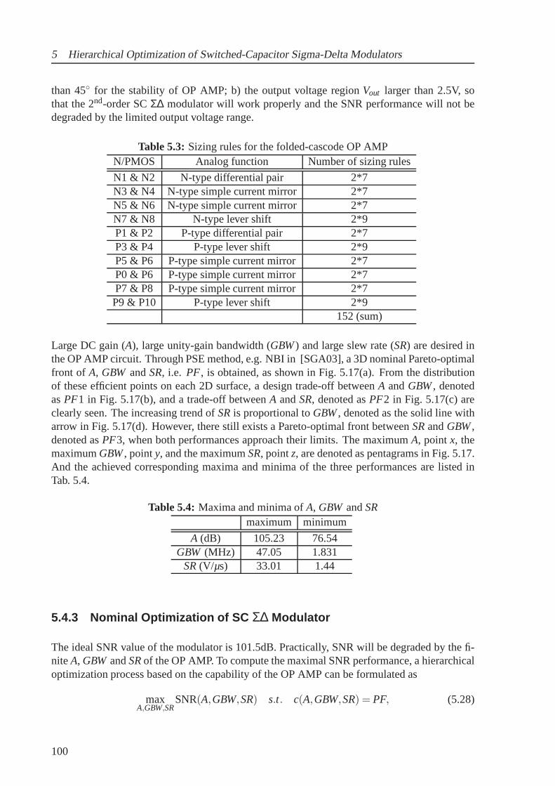
5 Hierarchical Optimization of Switched-Capacitor Sigma-Delta Modulators
than 45 for the stability of OP AMP; b) the output voltage regionVout larger than 2.5V, sothat the 2nd-order SCΣ∆ modulator will work properly and the SNR performance will not bedegraded by the limited output voltage range.
Table 5.3: Sizing rules for the folded-cascode OP AMPN/PMOS Analog function Number of sizing rules
N1 & N2 N-type differential pair 2*7N3 & N4 N-type simple current mirror 2*7N5 & N6 N-type simple current mirror 2*7N7 & N8 N-type lever shift 2*9P1 & P2 P-type differential pair 2*7P3 & P4 P-type lever shift 2*9P5 & P6 P-type simple current mirror 2*7P0 & P6 P-type simple current mirror 2*7P7 & P8 P-type simple current mirror 2*7P9 & P10 P-type lever shift 2*9
152 (sum)
Large DC gain (A), large unity-gain bandwidth (GBW) and large slew rate (SR) are desired inthe OP AMP circuit. Through PSE method, e.g. NBI in [SGA03], a3D nominal Pareto-optimalfront of A, GBW andSR, i.e. PF, is obtained, as shown in Fig. 5.17(a). From the distributionof these efficient points on each 2D surface, a design trade-off betweenA andGBW, denotedasPF1 in Fig. 5.17(b), and a trade-off betweenA andSR, denoted asPF2 in Fig. 5.17(c) areclearly seen. The increasing trend ofSRis proportional toGBW, denoted as the solid line witharrow in Fig. 5.17(d). However, there still exists a Pareto-optimal front betweenSRandGBW,denoted asPF3, when both performances approach their limits. The maximum A, pointx, themaximumGBW, pointy, and the maximumSR, pointz, are denoted as pentagrams in Fig. 5.17.And the achieved corresponding maxima and minima of the three performances are listed inTab. 5.4.
Table 5.4: Maxima and minima ofA, GBW andSRmaximum minimum
A (dB) 105.23 76.54GBW (MHz) 47.05 1.831
SR(V/µs) 33.01 1.44
5.4.3 Nominal Optimization of SC Σ∆ Modulator
The ideal SNR value of the modulator is 101.5dB. Practically, SNR will be degraded by the fi-niteA, GBWandSRof the OP AMP. To compute the maximal SNR performance, a hierarchicaloptimization process based on the capability of the OP AMP can be formulated as
maxA,GBW,SR
SNR(A,GBW,SR) s.t. c(A,GBW,SR) = PF, (5.28)
100
5.4 Example: Hierarchical Optimization of a2nd-order SCΣ∆ Modulator
PF
2P
F1
PF
3
y
z
x
y
PF
(a)
(b)
(c)
(d)
Figure 5.17: Pareto-optimal front of OP AMP (a)3D dimension;Projection on 2D surface (b)A vs. GBW; (c) A vs. SR; (d) SRvs. GBW
101

5 Hierarchical Optimization of Switched-Capacitor Sigma-Delta Modulators
wherec(∗) describes the feasible ranges of the system-level design parameters:A, GBWandSR,as shown in Fig. 5.17(a). However, the trade-off betweenGBW andSRis not obvious, whichresults in a narrow 3D Pareto-optimal front as shown in Fig. 5.17(a). It is difficult to fittingthePF. Moreover, an inaccurate fitting could result in a false design result. Hence, we try toreduce the number of the system-level design parameters first. Six system-level sweep-analysisprocesses of SNR are executed at design pointsx,y,z, respectively. For example a sweep-analysis at pointx, (i.e. maximalGBW), one of the other two parameters (A andSR), variesfrom their own minimum to maximum individually and the otherparameters keep constant atthe corresponding design values.
At point x, the red lines in Fig. 5.18 represent the variation of SNR related toA andSRrespec-tively. As can be seen, SNR increases withSR, while SNR stays almost constant withA. Atpoint y, the blue lines represent the variation of the SNR related toSRandGBW respectively.Worth to note, SNR keeps almost 0 withGBW, becauseSRis minimal at the design point. Atpoint z, the green lines represent the variation of the SNR related to SRandA respectively.Based on these results, we can find thatA doesn’t have any impact on SNR in this experiment,while SNR is very sensitive to the value ofSR. Additionally, a largerGBW can enlarge SNRwhenSRis maximal.
1 2 3 4 5 60
10
20
30
40
50
60
70
80
90
100
Parameters sweep from Min to Max respectively
SN
R (
dB)
SNR vs. ASNR vs. SRSNR vs. GBWSNR vs. SRSNR vs. GBWSNR vs. A
@ point x
@ point y
@ point z
Figure 5.18: SNR vs Parameter Sweep
Based on the analysis above, SNR is mostly dominated bySR. And the main increasing trend ofSRis proportional toGBW. Therefore, the maximal SNR is achieved by a design point, whichlies on the nominal Pareto-optimal frontPF3, zoomed in Fig. 5.19. The optimization of SNRin Equation 5.28 can be simplified to
maxGBW,SR
SNR(GBW,SR) s.t. c(GBW,SR) = PF3, (5.29)
102

5.4 Example: Hierarchical Optimization of a2nd-order SCΣ∆ Modulator
where the system-level design parameters are reduced toGBWandSR, PF3 is the optimizationconstraint for system-level optimization. The maximal SNRis 98.89dB generated by the designpointq1, which is listed in Tab. 5.6 and denoted as diamond in Fig. 5.19.
2.5 3 3.5 4 4.5
x 107
2.6
2.8
3
3.2
3.4x 10
7
GBW
SR
q1
q2
PF3
PF3WC
with yield of 99.87%
Figure 5.19: Pareto-optimal front of GBW vs. SR
5.4.4 Worst-Case Analysis of SC Σ∆ Modulator
What is the SNR performance with the nominal optimized device sizes actually after fabri-cation? Through a Monte Carlo analysis on the statistical parameters of the OP AMP, about52% circuits can generate theq1 performance values, i.e.GBW=35.05MHz andSR=32.97V/µs.Additionally, two operation parameters are considered here, the supply voltage, which variesfrom 2.9V to 3.1V, and the temperature, which varies from 0C to 100C. The worst-case op-eration conditions forSRandGBW are listed in Tab. 5.5. Consequently, only 0% circuits canachieve theq1 performance values in terms of both variation of statistical and operation para-meters. Therefore, the SNR of 98.89dB, which is generated bydesign pointq1, is not an actualcapability of the circuit after fabrication.
Table 5.5: Worst-case operation conditions forGBW andSRTemperature Supply voltage
GBW 100C 2.9VSR 0C 2.9V
To get the real maximum of SNR after fabrication, a yield-aware optimization is needed. Ac-cording to varied target yields, different worst-case-aware Pareto-optimal fronts can be ex-tracted. Fig. 5.19 shows a frontPF3WC with a target yield of 99.87% when the worst-casedistanceβw is set to 3, according to Tab. 3.1. The optimization of SNR with the 99.87% yieldcan be formulated as
maxGBW,SR
SNR(GBW,SR) s.t. c(GBW,SR) = PF3WC. (5.30)
103
5 Hierarchical Optimization of Switched-Capacitor Sigma-Delta Modulators
The achieved maximal SNR is 89.4dB, the corresponding design pointq2 is listed Tab. 5.6 anddenoted as diamond in Fig. 5.19. The maximal value of SNR is obviously degraded by thestatistical and operation parameters. Finally, the robustdesign results that we are searching forare the device sizes which generateq2, notq1.
Table 5.6: Nominal and robust optimization results of the ModulatorSNR Yield GBW SR(dB) (MHz) (V/us)
Ideal 101.5 infinite infiniteNominalq1 98.8 0% 35.05 32.97Robustq2 89.5 99.87% 28.32 26.3
5.5 Summary
This chapter describes the basic advantages by usingΣ∆ modulators compared to Nyquist-frequency modulators. Noise averaging and noise shaping issimultaneously implemented intheΣ∆ modulators. The efficiency of the 2nd-order SCΣ∆ modulator is discussed compared toother modulator topologies.
Based on the linearz-domain model of the 2nd-order SCΣ∆ modulator topology, the maximaltheory value of SNR can be evaluated. Due to the non-idealities of the analog building blocks,the actual maximum of SNR will be less than the theoretical value. Most non-idealities ofthe 2nd-order SCΣ∆ modulator are listed here and their effects on the SNR performance arepresented individually. And the corresponding models in SIMULINK are built including thesenon-idealities.
Since the simulation of a SCΣ∆ modulator on circuit level is very time-consuming, the proposedhierarchical optimization methodology in Chapter 3 is applied on the modulator. The SNRperformance is maximized based on the real capability of a fold-cascode OP AMP circuit. Inthe optimization process, a performance space explorationmethod is firstly applied to the OPAMP so that a nominal Pareto-optimal front is extracted, andthen the worst-case analysis isconducted on each efficient point of the nominal Pareto-optimal front, in order to obtain aworst-case-aware Pareto-optimal front. Based on that, thepractical maximum of SNR with atarget yield has been computed. It gives designers a real insight into the capability of the circuitafter fabrication. The presented method is not limited to the 2nd-order SCΣ∆ modulator butapplicable to other modulators as well.
104

Chapter 6
Conclusion
The Semiconductor Industry Association (SIA) has announced that worldwide semiconductorsales reached totaling $267.5 Billion in 2007, a new industry record. Analog circuits are oneof the fastest-growing segments of the market. In the next five years, nearly 70 percent of allICs will have analog signal components, which are widely used in communication, computer,consumer, automotive and industrial applications. The gradually shrinking process technologiesmake analog circuits smaller, faster and more power efficient, but introduce more challengesand difficulties as well. The increasing time-to-market pressure drives the progress of designmethodologies, CAD tools and design flows. In contrast to thesignificant increasing densityand complexity of analog circuits, design methodologies onanalog circuits have achieved a littleprogress over the past decades. Compared to the well developed and widely available digitalCAD tools, few robust commercial CAD tools are available except for spice-like numericalsimulators. Consequently, the design of analog and mixed-signal ICs remains still a long anderror prone process, which tends to be a bottleneck point in design process of SoC systems.Therefore, an efficient design methodology for large-scaleanalog/mixed-signal circuit designwill be valuable.
Chapter 1 presented the challenges of analog design. Compared to digital design, designers haveto be much more involved in the design process of an analog design than that of a digital design,and consequently the design results are highly dependent onthe knowledge and experiencesof individual designers. The current analog design flow starts with the manual selection ofcircuit topology. Then designers assign the transistor sizes and the values for resistors andcapacitors, and simulate the circuit. The tuning process ondesign parameters and the circuitverification have to been repeated until the desired circuitperformances are achieved. Somecommercial automatic sizing tools have been mentioned, which are capable of acceleratingsome analog designs. As analog circuits become larger, morecomplex and include digitalparts gradually, two different optimization strategies for large-scale analog/mixed-signal circuitshave been introduced: i.e. flat and hierarchical optimization methodology. Additionally, themethods for performance space exploration have been also summarized, which provide theuseful information of the lower-level realization for the design on a higher-level in hierarchy.
Chapter 2 explained the two automatic processes for analog design, i.e. automatic sizing andperformance space exploration. The fundamental concepts of analog design, e.g. design para-meter, circuit performance/specification/yield, circuitsimulation, have been introduced. Nom-
105

6 Conclusion
inal design aims to optimize the often conflicting circuit performances at the same time, whilerobust design aims to maximize the circuit yield. The automatic sizing process is a mappingfrom circuit specifications to design parameters, and is usually referred to as a nominal de-sign process. The additional sizing rules for CMOS transistors intend to reduce the degree offreedom in analog design, so that the automatically sized results are guaranteed to stay in thetechnically meaningful regions. Performance space exploration is a mapping from the feasiblespace of the design parameters to the feasible space of the circuit performances. A determinis-tic and simulation-based PSE method, i.e. Normal-BoundaryIntersection, has been introducedto generate a Pareto-optimal front (a part boundary of the entire feasible performance region),which represents the performance capabilities of the circuit.
Chapter 3 proposed a hierarchical optimization methodology for large-scale analog/mixed-signal circuits. The methodology is a"simulation-in-a-loop"-based hierarchical optimizationmethodology, which consists of four main steps. (1) Performance space exploration is appliedto each building block on the circuit level individually. Their respective Pareto-optimal frontscan be obtained. (2) Efficient behavioral models are built inHDLs or SIMULINK. The modelsinclude not only the description of circuit functionalities, but the description of Pareto-optimalfronts as well. (3) Based on these behavioral models, an automatic sizing process is conductedon the system level. During the optimization process, the system-level parameters are restrictedto these Pareto-optimal fronts. (4) The specifications for each building block are propagatedfrom the optimized results on the system level. And then, theautomatic sizing process on eachbuilding block is conducted individually and in parallel. The whole hierarchical optimizationprocess can be characterized by a bottom-up extraction of circuit capability and a top-downhierarchical sizing process. Additionally, through worst-case analysis on the efficient pointsof the nominal Pareto-optimal front, a worst-case-aware Pareto-optimal front can be extracted.Based on that, the obtained optimization results representthe actual circuit capability with atarget yield after fabrication.
In this thesis, the proposed hierarchical optimization methodology has been applied to two typ-ical large-scale analog/mixed-signal circuits: a charge-pump phase-locked loop (CPPLL) and aswitched-capacitor sigma-delta (SCΣ∆) modulator. In Chapter 4, the fundamental of a CPPLLhas been discussed, including PLL’s building blocks, PLL’sperformances and PLL system’sanalysis methods. The complex trade-offs in PLLs show the difficulties and the challengesof the optimization task by manual design. The time-consuming simulation of PLL’s perfor-mance is the main obstacle to the “simulation-in-a-loop”-based optimization method. To tacklethe problem, efficient behavioral models in Verilog-A have been developed. Based on perfor-mance space exploration on the circuit level, a first-time-successful top-down sizing processwithout iteration has been realized. The obtained Pareto-optimal fronts of building blocks andsystem represent the capability of circuit and visualize the conflicting relationship among per-formances, which give designers a detailed insight into thecircuit. In Chapter 5, a second-orderSC∆Σ modulator has been taken as example circuit because of its efficiency. Based on the lin-earz-domain model, the theoretic maximum SNR performance can beevaluated. However dueto the non-idealities of the analog building blocks, the actual SNR performance cannot achievethe theoretical value. By applying performance space exploration on building blocks, the SNRperformance has been maximized while considering the capabilities of OP AMP. Moreover,worst-case analysis has been applied to the nominal efficient points in order to extract a worst-case-aware Pareto-optimal front. Based on it, the actual maximum of the SNR with a target
106

yield has been extracted. The final optimized result show theeventual capability of the cir-cuit after fabrication. The “simulation-in-a-loop”-based optimization method has been realizedbased on the efficient behavioral modeling in SIMULINK.
With the proposed hierarchical approach, the complete CPPLL and the SCΣ∆ modulator havebeen sized algorithmically despite their design complexity. Moreover, the whole design processcan be accomplished in a reasonable time cost, which is obviously shorter than the design periodby using the traditional analog design method. The presented approach is not limited to the twokinds of circuits but applicable to other large-scale analog/mixed-signal circuits as well.
107


Appendix A
Analog Sizing Rules
For analog circuits using CMOS technology, a lot of fundamental analog building blocks areidentified based on [GZEA01]. There are five levels of hierarchy as depicted in Tab. A.1 [Ste05].∗
• At the lowest hierarchy level 0, the atomic building block isa single transistor. A transistorcan act as a voltage-controlled current source(VCCS) in itssaturation operation range or avoltage-controlled resistor in its linear operation range.
• At the hierarchy level 1, seven transistor pairs are defined to present basic analog function-alities. For example, a simple current mirror is used to copya current from one path toanother path. A level shift is used to shift a voltage to a higher or a lower voltage level.
• At the hierarchy level 2, four “pairs of transistor pairs” are defined to present more complexor more accurate analog function. These pairs are consistedof the structures from level0 and level 1. For example, a 4-transistor can be modeled as a combination of a voltagereference and a current mirror load.
• At the hierarchy level 3, a cascode current mirror bank is modeled as a level shifter bankand a current mirror bank.
• At the hierarchy level 4, a differential stage is modeled as acombination of a differentialpair and a generic current source. The current source can be implemented as a simplecurrent mirror or a cascode mirror structure.
As can be seen, the block at a certain hierarchy level is composed of blocks at lower levels.Moreover, the structure library is not complete and a variety of other building blocks can beadded.
A set of sizing rules will be given for each building block. Theses sizing constraints guaran-tee the dedicated analog function and strengthen its robustness, e.g. reduce mismatch effect orchannel length modulation. These constraints refer to not only transistor geometry parameters(width, length and area) and electrical transistor quantities (e.g. transistor drain/source volt-ages) as well. Since each block on leveli consists of the building blocks at the lower levels inhierarchy, therefore the sizing rules for each identified block at leveli include all sizing rules
∗ In this table, fundamental analog building blocks are presented schematically through NMOS transistors andanalogously for PMOS counterparts.
109

A Analog Sizing Rules
Table A.1: Library of analog basic building blocks [Ste05]Function Schematic (NMOS) Hierarchy
(PMOS analogously) Level
Voltage-controlled resistor (res)Voltage-controlled current source (cs) 0
Simple current mirror (cm) 1
Level shifter (ls)
Voltage reference 1 (vr1)
Current mirror load (cml)
Differential pair (dp)
Voltage reference 2 (vr2)
Flip-flop (ff)
Level shifter bank (LSB) 2
Current mirror bank (CMB)
Cascode current mirror (CCM)
4-Transistor current mirror (4TCM)
Cascode current mirror bank (CCMB) 3
Differential stage(CM ∈ cm, CCM, 4TCM, CCMB)
(DST)CM
4
110

of these fundamental blocks and the additional sizing rulesfor the block itself. Tab. A.2 [mun]lists the detailed sizing rules for the recognized basic NMOS structures: simple current mirror,differential pair and level shifter. The safety marginm is set according to the CMOS realizationtechnology.
Table A.2: Sizing rules for NMOS basic structures [mun]Structure Constraint Safety margin Reason
NMOS Current Mirror
VGS−Vth ≥ m m= 100mV inversionVDS− (VGS−Vth) ≥ m m= 100mV saturationL ·W ≥ m m= 1µm2 limit Vth mismatchL ≥ m m= 0.5µm limit relative variance ofW ≥ m m= 0.5µm the transconductance factor−m≤VDS1−VDS2≤ m m= 200mV reduce the influence of the channel
length modulation factor on thecurrent transmission coefficient
equal length limit systematic mismatches
NMOS Differential
Pair
VGS−Vth ≥ m m= 10mV inversionVDS− (VGS−Vth) ≥ m m= 10mV saturationL ·W ≥ m m= 1µm2 limit Vth mismatchL ≥ m m= 0.5µm limit relative variance ofW ≥ m m= 0.5µm the transconductance factorVGS−Vth ≤ m m= 1.0V reduce the influence of
transconductance mismatchon the input offset
−m≤VDS1−VDS2≤ m m= 200mV reduce the influence of the channellength modulation factor on thecurrent transmission coefficient
equal length avoid transconductance mismatchequal width and input offset voltage mismatch
NMOS Level Shifter
VGS−Vth ≥ m m= 10mV inversionVDS− (VGS−Vth) ≥ m m= 10mV saturationL ·W ≥ m m= 1µm2 limit Vth mismatchL ≥ m m= 0.5µm limit relative variance ofW ≥ m m= 0.5µm the transconductance factor−m≤ iDS2/iDS2−W2/W1 ≤ m m= 0.2 avoid a difference between the
effective voltageVGS
equal length avoid transconductance mismatch
111

A Analog Sizing Rules
112

Appendix B
Modeling Σ∆ Modulator Non-Idealities inSIMULINK
In this chapter, the behavioral model of the second-orderΣ∆ modulators is realized in Simulinkmodule, which are based on the modules in [BFM+99,MBF+03].
Sampling Jitter According to Equation 5.11, a random sampling jitter model can be built asshown in Fig. B.1. The input signalx(t) and its derivativedu/dt are continuous-time signals.They are sampled with a sampling periodTs by a zero-order hold. The sampling uncertainty,i.e. clock jitterδ, is implemented by a Gaussian random processn(t) with a standard deviation∆τ.
1
y(t)
Zero−OrderHold
Zero−OrderHold
RandomNumber
Product
delta
Jitter Standard Divation
du/dt
Derivative
Add
1
x(t)
n(t)
Figure B.1: Modeling a random sampling jitter [MBF+03]
Switches Thermal Noise The switch thermal noise voltageeT can be evaluated by Equa-tion 5.12. And the thermal noise is superimposed to the inputvoltagex(t), expressed as
y(t) = [x(t)+eT(t)]b= [x(t)+
√
kTCs
n(t)]b, (B.1)
wheren(t) denote a Gaussian random process with unity standard deviation, andb = Cs/Cf isthe coefficient of the integrator. Equation B.1 is implemented by the model shown in Fig. B.2.
113

B ModelingΣ∆ Modulator Non-Idealities in SIMULINK
T
1
y(t)b
Zero−OrderHold
RandomNumber
Product1
Product
f(b)
KT/C noise
Add
1
x(t)
e (t)
Figure B.2: Modeling switches thermal noiseKT/C block [MBF+03]
Operation Amplifier Noise The model of OP AMP noise is shown in Fig. B.3. The intrinsicnoise of operational amplifier includes thermal noise, flicker (1/f) noise, shot noise etc. Thesevarious noises contribute together to the total OP AMP noisepowerV2
n , whose value can beevaluated through simulation on the circuit in Fig. 5.3 during phaseφ2. "The resulting outputreferred noise PSD has to be integrated over the whole frequency spectrum, eventually takinginto account the degradation of the thermal noise PSD introduced by the auto-zero or corre-lated double sampling techniques" [ET96], and then dividedby b2 in order to calculate thecorresponding input-referred rms noise voltageVn.
1
y(t)
b
Zero−OrderHold
RandomNumber
ProductVn
Noise Standard Divation
Figure B.3: Modeling operational amplifier noise [MBF+03]
Real Integrator Fig. B.4 shows the model of a real integrator including all the non-idealitieslisted in Sec. 5.3.1.3. Only a fraction (1−α) of the previous output of the integrator is added(fed back) to each new input sample, which is modeled the parameter ’alpha’ in Fig. B.4, where
alpfa= 1−α =A0−1
A0. (B.2)
The finite bandwidth and slew rate of the OP AMP are implemented by a MATLAB functionblock which is placed in front of the integrator. According to Equation 5.23, the correspondingdescription in C-code is shown as follows. The limited output range of the OP AMP can besimply realized by using a saturation block to limit the finaloutput range.
function out = slew(in,alpha,sr,GBW,Ts)% Models the operational amplifier finite bandwidth and slew rate% for a discrete time integrator
114

% out = slew(in,alpha,sr,GBW,Ts)% in: Input signal amplitude% alpfa: Effect of finite gain (ideal amplifier alpha=1)% sr: Slew rate in V/s% GBW: Gain-bandwidth product of the integrator loop gain in Hz% Ts: Sample time in s% out: Output signal amplitude
tau=1/(2*pi*GBW); % Time constant of the integratorTmax = Ts/2;slope=alpha*abs(in)/tau;
if slope > sr % Op-amp in slewingtsl = abs(in)*alpha/sr - tau; % Slewing timeif tsl >= Tmax
error = abs(in) - sr*Tmax;else
texp = Tmax - tsl;error = abs(in)*(1-alpha) + (alpha*abs(in) - sr*tsl) * exp(-texp/tau);
endelse % Op-amp in linear region
texp = Tmax;error = abs(in)*(1-alpha) + alpha*abs(in) * exp(-texp/tau);
end
out = in - sign(in)*error;
1
y(t)
alpfa
leakage
z
1
Unit Delay Saturation
MATLABFunction
GBW & SRAdd
1
x(t)
Figure B.4: Modeling real integrator [MBF+03]
115

B ModelingΣ∆ Modulator Non-Idealities in SIMULINK
116

Appendix C
Phase Noise & Jitter
C.1 Relationship between Phase Noise and Jitter
Analog engineers prefer using phase noise, while digital designers prefer using jitter. The re-lationship between the two parameters is briefly described here. More details can be foundin [Raz96,DMR00,HL98,HLL99,LH00,Meh02].
Timing jitter is defined as the standard deviation of the timeuncertainty [HLL99]:
σ2∆T =
1
ω20
·E[φ(t +∆T)−φ(t)]2 =1
ω20
· E[φ2(t +∆T)+φ2(t)−2φ(t +∆T) ·φ(t)], (C.1)
where E[·] represents the expected value, the time uncertainty isφ(t + ∆T)− φ(t). SinceE[φ(t) · φ(t + ∆T)] is equal to the autocorrelation ofφ(t), i.e. Rφ(∆T). Therefore, the jitterin Equation C.1 can be written as
σ2∆T =
2
ω20
[Rφ(0)−Rφ(∆T)]. (C.2)
The relationship between the autocorrelation and the powerspectrum is given by the Khinchintheorem [Gar90], i.e.
Rφ(τ) =Z ∞
0Sφ( f )ej2π f τd f, (C.3)
whereSφ( f ) represents the power spectrum ofφ(t). Replacing the autocorrelation of Equa-tion C.3 into Equation C.2 result in
σ2∆T =
8
w20
Z ∞
0Sφ( f )sin2(π f ∆T)d f. (C.4)
Equation C.4 describes the relationship between timing jitter and noise power spectral density(psd). Therefore, the timing jitter can be calculated from the phase noise by using Equation C.4.As ∆T goes to infinity, timing jitter is calculated from Equation C.2:
σ2∆T→∞ =
2
ω20
[Rφ(0)] (C.5)
σ2∆T→∞ =
2
ω20
Z ∞
0Sφd f. (C.6)
117

C Phase Noise & Jitter
As can be seen from the above analysis, since time jitter has less information than phase-noisespectrum, the inverse process (from jitter to phase noise) is normally not feasible, unless theextra information on the shape of phase-noise spectrum is available.
C.2 Extracting Jitter from Phase Noise Analysis on PFD/CPand VCO Blocks
Simulator SpectreRF [Cadb] is used in this thesis to computethe phase noise of the CPPLL. Theproper frequency range in periodic-steady-state (PSS) analysis and PNoise analysis is chosen sothat the noise out of the frequency range is neglected∗. In PSS and PNoise analysis, it linearizesthe circuit at each time step in a given period and accumulates the contributions from everynoise sources and over each time point to compute the total phase noise.
The jitter of PFD/CP can be derived from the following steps.First of all, according to theedge-to-edge jitter definition, i.e.
var(δtn) = E[(δtn− δtn)2], (C.7)
where ¯δtn is the mean value ofδtn. The value is equal to 0 for a white noise. Therefore, thevar(δtn) can be reformulated as
var(δtn) = E[(δtn)2] = Rδtn(0). (C.8)
Applying the Wiener-Khinchin Theorem in Equation C.3 to determine
var(δtn) =Z ∞
0Sn( f )d f, (C.9)
whereSn( f ) is the power spectral density of theδtn sequence.
To reduce the simulation time on jitter extraction, the noise source of PFD/CP is moved forwardat its input, which is called input-referred jitter of PFD/CP. The corresponding input-referredjitter can be calculated by dividing the effective gain of the PFD/CP:
JeePFD/CP =T
Kdet
√
var(δn)
2, (C.10)
whereKdet is the gain of the PFD/CP, in units of ampleres/cycle,T is in units of seconds/cycle.The ratio 2 comes from the modeling on two transition edges ina cycle.The jitter in VCO, is almost completely due to oscillator phase noise. According to the Equation76 in [Kun05], i.e.
c = L(∆ f )∆ f 2
f 20
, (C.11)
∗ The noise should be at least -40dB down and dropping at the highest frequency simulated. In a cycle with two transition, the sum jitter is calculated by Jsum=√
J21 +J2
2 =√
2J, whereJ1 = J2 = J
118

C.2 Extracting Jitter from Phase Noise Analysis on PFD/CP and VCO Blocks
and Equation 73 in [Kun05], i.e.
J =√
cT =
√
cf0
, (C.12)
the jitter of VCO can be extracted by
JVCO =∆ ff 1.510
L(∆ f )20 . (C.13)
L(∆ f ) means the phase noise on the offset frequency∆ f in unit of dBc/Hz. Note the EquationC.13 is only valid when the phase noise at∆ f , which is in the 1/ f 2 region.
119

C Phase Noise & Jitter
120

Appendix D
CPPLL’s Verilog-A Models
In this chapter, the Verilog-A models for building blocks ofthe CPPLL are listed in the follow-ing, which are based on the modules in [Kun05].
Lists D.1- D.4 are for the extraction of the locking time performance.
Listing D.1: Behavioral model of PFD in Verilog A / / PFD
‘ i n c l u d e " c o n s t a n t s . h "‘ i n c l u d e " d i s c i p l i n e . h "
module PFD ( re f , feedback , u , ub , db , d ) ;inpu t r e f , f eedback ; / / i n p u t and feedback are t h e r e f e r e n c e and feedback c l o c koutput u , ub , db , d ;e l e c t r i c a l re f , feedback , u , ub , db , d ;
parameter r e a l v_h igh =3;parameter r e a l v_low =0;parameter r e a l t t o l =10p ;parameter r e a l t t =120 p from ( 0 : 1 0 0 0 0 0 0 ) ; / / r i s e t ime and f a l l t ime/ / f o r "u " and " ub " s i g n a l : de lay t ime e x t r a c t e d from c i r c u i tl e v e l s i m u l a t i o n/ / −−−−−−−−−− r i s e dea ly −−−−−−−−−−−−− f a l l de layparameter r e a l td_u1 =37p ; parameter r e a l td_u2 =190 p ;/ / f o r "d " and " db " s i g n a l :parameter r e a l td_d1 =45p ; parameter r e a l td_d2 =136 p ;
i n t e g e r s t a t e ; / / s t a t e =−1 f o r down , s t a t e =1 f o r up .r e a l td_u , td_ub , td_d , td_db ; / / de lay t ime
ana log begin@( c r o s s (V( r e f )−v_h igh / 2 . 0 , 1 , t t o l ) ) begin
i f ( s t a t e <1)s t a t e = s t a t e +1;
/ / $ s t r o b e ( " c u r r e n t t ime %g ns and s t a t e =" , $ r e a l t i m e* 10e8 , s t a t e ) ;i f (V( u ) >v_h igh / 2 ) td_u = td_u1 ; e l s e td_u = td_u2 ;i f (V( ub ) > v_h igh / 2 ) td_ub = td_u1 ; e l s e td_ub = td_u2 ;i f (V( d ) >v_h igh / 2 ) td_d = td_d1 ; e l s e td_d = td_d2 ;i f (V( db ) > v_h igh / 2 ) td_db = td_d1 ; e l s e td_db = td_d2 ;
end
@( c r o s s (V( feedback )−v_h igh / 2 . 0 , 1 , t t o l ) ) begini f ( s t a t e >−1)
s t a t e = s t a t e−1;i f (V( u ) >v_h igh / 2 ) td_u = td_u1 ; e l s e td_u = td_u2 ;i f (V( ub ) > v_h igh / 2 ) td_ub = td_u1 ; e l s e td_ub = td_u2 ;i f (V( d ) >v_h igh / 2 ) td_d = td_d1 ; e l s e td_d = td_d2 ;i f (V( db ) > v_h igh / 2 ) td_db = td_d1 ; e l s e td_db = td_d2 ;
121

D CPPLL’s Verilog-A Models
end
V( u ) <+ t r a n s i t i o n ( ( s t a t e ==+1) ? v_h igh : 0 . 0 , td_u , t t ) ;V( ub )<+ t r a n s i t i o n ( ( s t a t e ==+1) ? 0 . 0 : v_high , td_ub , t t / 2. 0 ) ;V( d ) <+ t r a n s i t i o n ( ( s t a t e ==−1) ? v_h igh : 0 . 0 , td_d , t t ) ;V( db )<+ t r a n s i t i o n ( ( s t a t e ==−1) ? 0 . 0 : v_high , td_db , t t / 2 . 0 ) ;
endendmodule
Listing D.2: Behavioral model of CP in Verilog A / / CP
‘ i n c l u d e " c o n s t a n t s . vams "‘ i n c l u d e " d i s c i p l i n e s . vams "
module CP( Iou t , Down , N_Down , N_Up , Up , I b i a s ) ;inpu t Up , N_Up , Down , N_Down ;output I o u t ;e l e c t r i c a l Up , N_Up , Down , N_Down , I o u t ;
parameter r e a l v_h igh = 3 ;parameter r e a l v_low = 0 ;parameter r e a l v_th =( v_high−v_low ) / 2 ; / / t h r e s h o l d v o l t a g eparameter r e a l TransTime=10p from ( 0 : 1 0 0 0 0 0 0 ) ;parameter r e a l Delay =1p from ( 0 : 1 0 0 0 0 0 0 ) ;parameter r e a l Ip =25.0 e−6; / / charge pump ’ s o u t p u t c u r r e n tparameter r e a l v_max = 2 . 8 5 ; / / maximum v o l t a g e a t o u t p u t node so t h a t
/ / Pmos c u r r e n t sou rce in s a t u r a t i o nparameter r e a l v_min = 0 . 3 5 ; / / minimum v o l t a g e a t o u t p u t node so t h a t
/ / Nmos c u r r e n t sou rce in s a t u r a t i o nparameter r e a l Mis = 0 . 0 0 ; / / Mismatch o f up and down c u r r e n t
i n t e g e r s t a t e ; / / CP s t a t e : "−1−>charge ","1−> d i s c h a r g e ","0−>no o u t p u t c u r r e n t "
ana log begin@( i n i t i a l _ s t e p ) begin
s t a t e =0;end@( c r o s s (V(Up)−v_th , 1 ) ) begin / / c u r r e n t charge
s t a t e = −1;end@( c r o s s (V(Down)−v_th , 1 ) ) begin / / c u r r e n t d i s c h a r g e
s t a t e = 1 ;end@( c r o s s (V(Up)−v_th , −1)) begin / / no o u t p u t c u r r e n t
s t a t e =0;end@( c r o s s (V(Down)−v_th , −1)) begin
s t a t e =0;end
/ / r e s t r i c t t h e o u t p u t v o l t a g e range from v_min to v_max@( c r o s s (V( I o u t )−v_max , 1 ) ) begin
s t a t e =0end@( c r o s s (V( I o u t )−v_min , −1))begin
s t a t e =0;end
I ( I o u t )<+ t r a n s i t i o n ( Ip* s t a t e* (1+ s t a t e* Mis ) , Delay , TransTime ) ;
endendmodule
Listing D.3: Behavioral model of VCO in Verilog A
122

/ / VCO
‘ i n c l u d e " d i s c i p l i n e . h "‘ i n c l u d e " c o n s t a n t s . h "
module vco ( V_tune , VCO_out ) ;inpu t V_tune ;output VCO_out ;e l e c t r i c a l V_tune , VCO_out ;
parameter r e a l VSS=0 , VDD=3;parameter r e a l Vmin = 0 . 6 ;parameter r e a l Vmax=2.6 from ( Vmin :10 e5 ) ;parameter r e a l Fmin=50 e6 from ( 0 : 1 0 e9 ) ;parameter r e a l Kvco=600 e6 ;parameter r e a l t t =0 . 0001 / Fmin from ( 0 : 1 0 e3 ) ;parameter r e a l t t o l =1e−8/Fmin from ( 0 : 1 / Fmin ) ;
r e a l f r eq , phase , Vout ;
ana log begin@( i n i t i a l _ s t e p )begin
Vout=VSS ;end
/ / compute t h e f r e q from t h e i n p u t v o l t a g ei f (V( V_tune )<=Vmin )
f r e q = Fmin ;e l s e i f (V( V_tune )<=Vmax )
f r e q = (V( V_tune )−Vmin)* Kvco+Fmin ;e l s e
f r e q = (V( V_tune )−Vmax )* ( 0 . 2 5* Kvco )+ ( Vmax−Vmin )* Kvco+Fmin ;
/ / i d e a l f u n c t i o n/ / f r e q =(V( V_tune )−Vmin )* Kvco + Fmin ;
/ / phase i s t h e i n t e g r a l o f t h e f r e q u e n c y modulo 1phase = idtmod ( f req , 0 . 0 , 1 . 0 ,−0.5) ;
/ / update j i t t e r t w i c e per per iod@( c r o s s ( phase−0.25 ,1 , t t o l ) )begin
Vout=VDD;end@( c r o s s ( phase +0 . 25 , 1 , t t o l ) )begin
Vout=VSS ;endV( VCO_out)<+ t r a n s i t i o n ( Vout , 0 , t t ) ;
endendmodule
Listing D.4: Behavioral model of divider in Verilog A / / d i v i d e r
‘ i n c l u d e " c o n s t a n t s . h "‘ i n c l u d e " d i s c i p l i n e . h "
module d i v i d e r ( c lock_ou t , c l o c k _ i n ) ;inpu t c l o c k _ i n ;output c l o c k _ o u t ;e l e c t r i c a l c lock_ in , c l o c k _ o u t ;
parameter r e a l Nmin = 6 ; / / minimum d i v i d e r va lueparameter r e a l Nmax = 20 ; / / maximum d i v i d e r va lueparameter r e a l v_h igh = 3 ;parameter r e a l v_low = 0 ;parameter r e a l v_th = 1 . 5 ;parameter r e a l t t = 10p ; / / t ime o f r i s e and f a l l t ime
123

D CPPLL’s Verilog-A Models
parameter r e a l t d = 0 ;parameter r e a l JumpTime=8u ; / / o u t p u t f r e q u e n c y jump from minimum maximum
i n t e g e r count , n ,M;
ana log begin
@( c r o s s ( (V( c l o c k _ i n )− v_th ) , 1 ) ) begini f ( $abs t ime >=JumpTime ) M=Nmax ;e l s e M=Nmin ;
coun t = coun t +1;i f ( count >=M) coun t =0;n = (2* coun t >= M) ;
end
V( c l o c k _ o u t )<+ t r a n s i t i o n ( n? v_h igh : v_low , td , t t ) ;
endendmodule
Lists D.5- D.8 are for the extraction of the jitter performance.
Listing D.5: Behavioral model of oscillator in Verilog A / / F ixed−f r e q u e n c y o s c i l l a t o r (OSC) w i th accumu la t ing and synch ronous j i t t e r
‘ i n c l u d e " d i s c i p l i n e s . h "
module OSC( ou t ) ;output ou t ;e l e c t r i c a l ou t ;
parameter r e a l f r e q =25 e6 from ( 0 : 1 0 e9 ) ;parameter r e a l r a t i o =1 from ( 0 : 1 0 e9 ) ;parameter r e a l VSS=0 , VDD=3;parameter r e a l t t =0.01* r a t i o / f r e q from ( 0 : 1 0 e9 ) ;parameter r e a l a c c J i t t e r =0 from [ 0 : 0 . 1 / f r e q ) ;
/ / pe r iod j i t t e r f o r r e f e r e n c e osc and d i v i d e rparameter r e a l s y n c J i t t e r =0 from [ 0 : 0 . 1* r a t i o / f r e q ) ;
/ / edge−to−edge j i t t e r , f o r d i v i d e r and PFD/CP
i n t e g e r n , accSeed , syncSeed ;r e a l next , dT , dt , accSD , syncSD , Jcp ;
ana log begin@( i n i t i a l _ s t e p ) begin
accSeed =286;syncSeed =−459;accSD= a c c J i t t e r* s q r t ( r a t i o / 2 ) ;syncSD= s y n c J i t t e r ;nex t = 0 . 5 / f r e q + $abs t im e ;
end
/ / c a l c u l a t i o n j i t t e r va lue from f i t t i n g f u c n t i o nJcp= f i t t i n g f u n c t i o n 1 ( I cp ) ;syncSD= Jcp ;
@( t i m e r ( nex t + d t ) )beginn =! n ;dT = accSD * $ d i s t _ n o r m a l ( accSeed , 0 , 1 ) ;d t = syncSD* $ d i s t _ n o r m a l ( syncSeed , 0 , 1 ) ;nex t = nex t +0.5* r a t i o / f r e q +dT ;
end
V( ou t )<+ t r a n s i t i o n ( n?VDD: VSS, 0 , t t ) ;endendmodule
124

Listing D.6: Behavioral model of PFD/CP in Verilog A / / Phase−Frequency D e t e c t o r w i th Charge Pump/ // / p fd_cp1 : a s imp le t h r e e s t a t e phase−f r e q u e n c y d e t e c t o r/ / V ers ion 1a , 12 J u l y 03/ // / Ken Kunder t/ // / Downloaded from The Des igner ’ s Guide (www. des igners−gu ide . org ) ./ / Pos t any q u e s t i o n s to www. des igners−gu ide . org / Forum
‘ i n c l u d e " d i s c i p l i n e s . vams "‘ i n c l u d e " c o n s t a n t s . vams "
/ // / Th is model e x h i b i t s no j i t t e r/ / The j i t t e r o f PFD/CP i s i n t e g r a t e d i n t o OSC b lock
module pfd_cp1 ( Iou t , r e f , vco ) ;
output I o u t ; e l e c t r i c a l I o u t ; / / c u r r e n t o u t p u tinpu t r e f ; v o l t a g e r e f ; / / p o s i t i v e i n p u t ( edge t r i g g e r e d )inpu t vco ; v o l t a g e vco ; / / i n v e r t i n g i n p u t ( edge t r i g g e r e d )parameter r e a l i o u t =20u ; / / maximum o u t p u t c u r r e n tparameter r e a l VDD= 1 . 8 ; / / o u t p u t v o l t a g e in h igh s t a t eparameter r e a l VSS=0; / / o u t p u t v o l t a g e in low s t a t eparameter r e a l Vth =(VDD+VSS ) / 2 ; / / t h r e s h o l d v o l t a g e a t i n p u tparameter i n t e g e r d i r =1 from [−1:1] exc lude 0 ;
/ / d i r =1 f o r p o s i t i v e edge t r i g g e r/ / d i r=−1 f o r n e g a t i v e edge t r i g g e r
parameter r e a l t t =1n from ( 0 : i n f ) ; / / t r a n s i t i o n t ime o f o u t p u t s i g n a lparameter r e a l t t o l =1p from ( 0 : i n f ) ;i n t e g e r s t a t e ;
ana log begin@( c r o s s (V( r e f )−Vth , d i r , t t o l ) ) begin
i f ( s t a t e > −1) s t a t e = s t a t e− 1 ;end@( c r o s s (V( vco)−Vth , d i r , t t o l ) ) begin
i f ( s t a t e < 1) s t a t e = s t a t e + 1 ;end
I ( I o u t ) <+ t r a n s i t i o n ( i o u t* s t a t e , 0 , t t ) ;
endendmodule
Listing D.7: Behavioral model of VCO with jitter in Verilog A / / VCO&D t o g e t h e r e x h i b i t s J i t t e r‘ i n c l u d e " d i s c i p l i n e . h "‘ i n c l u d e " c o n s t a n t s . h "
module VCO_Div ( V_tune , VCO_out ) ;inpu t V_tune ;output VCO_out ;e l e c t r i c a l V_tune , VCO_out ;parameter r e a l VSS=0 , VDD=3;parameter r e a l Vmin = 0 . 6 ;parameter r e a l Vmax=2.6 from ( Vmin :10 e5 ) ;parameter r e a l Kvco=600 e6 ;parameter r e a l Fmin=50 e6 from ( 0 : 1 0 e9 ) ;parameter r e a l t t =0 . 0001 / Fmin from ( 0 : 1 0 e3 ) ;parameter r e a l t t o l =1e−8/Fmin from ( 0 : 1 / Fmin ) ;parameter r e a l N=20; / / i f N!=1 , d i v i d e r moved i n t o t h e VCO b lockparameter r e a l I vco =400 e−6; / / c u r r e n t comsumptionparameter r e a l Jvco =10e−12; / / J i t t e r o f VCOr e a l f r eq , phase , dT , d e l t a , Vout ;i n t e g e r seed , fvco ;
125

D CPPLL’s Verilog-A Models
ana log begin@( i n i t i a l _ s t e p )begin
seed =160;Vout=VSS ;d e l t a =Jvco* s q r t (2* N ) ; / / c a l c u l a t i n g t h e co r respond ing j i t t e r on t h e d i v i d e r o u t pu t
end
/ / c a l c u l a t e t h e f r e q from t h e i n p u t v o l t a g ei f (V( V_tune ) <Vmin )
f r e q =Fmin ;e l s e i f (V( V_tune )<=Vmax )
f r e q =(V( V_tune )−Vmin )* Kvco + Fmin ;e l s e
f r e q =(V( V_tune )−Vmax )* ( 0 . 2 5* Kvco )+ ( Vmax−Vmin )* Kvco+Fmin ;
/ / app ly t h e f r e q u e n c y d i v i d e r , add t h e phase n o i s ef r e q = ( f r e q /N) / (1 + dT * f r e q / N ) ;
/ / c a l c u l a t i o n o f Jvco th rough f i t t i n g f u n c t i o nJvco= f i t t i n g f u n c t i o n 2 ( Ivco , Kvco ) ;
/ / phase i s t h e i n t e g r a l o f t h e f r e q u e n c y modulo 1phase = idtmod ( f req , 0 . 0 , 1 . 0 ,−0.5) ;
/ / update j i t t e r t w i c e per per iod@( c r o s s ( phase−0.25 ,1 , t t o l ) )begin
dT= d e l t a* $ d i s t _ n o r m a l ( seed , 0 , 1 ) ;Vout=VDD;
end@( c r o s s ( phase +0 . 25 , 1 , t t o l ) )begin
dT= d e l t a* $ d i s t _ n o r m a l ( seed , 0 , 1 ) ;Vout=VSS ;
endV( VCO_out)<+ t r a n s i t i o n ( Vout , 0 , t t ) ;
endendmodule
Listing D.8: Behavioral model of PLL outputs’period measurement in Verilog A / / V e r i l ogA f o r PLL_Ji t terMod , PLLoutput , v e r i l o g a‘ i n c l u d e " c o n s t a n t s . vams "‘ i n c l u d e " d i s c i p l i n e s . vams "
module PLLoutput ( VCO_out ) ;inpu t VCO_out ;e l e c t r i c a l VCO_out ;parameter r e a l t s t a r t = 20e−6; / / s t a r t to w r i t e an o u t p u t f i l eparameter r e a l VDD = 3 ;parameter r e a l VTH = VDD/ 2 ;i n t e g e r fp ;r e a l prev ;
ana log begin@( i n i t i a l _ s t e p )begin
fp =$fopen( " PLLPer iods . t c l " , "w" ) ;end@( c r o s s ( (V( VCO_out)−VTH) , 1 ) ) begin
i f ( $abs t ime >= t s t a r t ) $ f s t r o b e ( fp , " %3.10e " , $abs t ime−prev ) ;prev = $abs t im e ;
end@( f i n a l _ s t e p ) begin
$ f c l o s e( fp ) ;end
endendmodule
126

Bibliography
[Abi97] Asad Abidi. Analog circuit design-rf analog-to-digital converters sensor andactuator interfaces; low-noise oscillators, plls and synthesizers. chapter HowPhase Noise Appears in Oscillators. Kluwer Academic Publishers, 1997.
[AEGP00] K. Antreich, J. Eckmueller, H. Graeb, and M. Pronath. Wicked: Analog cir-cuit synthesis incorporating mismatch. InIEEE Custom Integrated CircuitsConference (CICC), pages 511–514, May 2000.
[AETL96] Brian A. A. Antao, Fatehy M. El-Turky, and Robert H.Leonowich. Behavioralmodeling phase-locked loops for mixed-mode simulation.Analog IntegratedCircuits and Signal Processing, (10):45–65, 1996.
[AGC94] K. Antreich, H. Graeb, and U. W. Claudia. Circuit analysis and optimizationdriven by worst-case distance.IEEE Transactions on Computer-Aided Designof Circuits and Systems, 13(1):57–71, Jan. 1994.
[AH06] Bashir Al-Hashimi.System-on-chip: Next Generation Electronics. IET, 2006.
[AN96] O. Aaserud and I. Ring Nielsen. Trends in current analog design¡ªa paneldebate.Analog Integrated Circuits and Signal Processing, (7):5–9, 1996.
[AP87] S. Ardalan and J. Paulos. An analysis of nonlinear behavior in delta-sigmamodulators. IEEE Transactions on Circuits and Systems, 34(6):593– 603,Jun. 1987.
[APT02] Peter J. Ashenden, Gregory D. Peterson, and DarrellA. Teegarden.The Sys-tem Designer’s Guide to VHDL-AMS. Morgan Kaufmann Publishers, SanFrancisco, 2002.
[Ass] Semiconductor Industry Association.Inernational Technology Roadmap forSemiconductors. 1999 edition.
[Bak04] R. Jacob Baker.CMOS: Mixed Signal Circuit Design. Wiley-IEEE Press,2004.
[Bes03] Roland E. Best.Phase-Locked Loops Design, Simulation, and Applications.Mc-Graw-Hill, 2003.
127

Bibliography
[BFM+99] S. Brigati, F. Francesconi, P. Malcovati, D. Tonietto, A. Baschirotto, andF. Maloberti. Modelling sigma-delta modulator nonidealities in simulink. InIEEE International Symposium on Circuits and Systems (ISCAS), pages 384–387, Jul. 1999.
[BGH04] O. Bajdechi, G. E. Gielen, and J. H. Huijsing. Systematic design exploration ofdelta-sigma adcs.IEEE Transactions on Circuits and Systems I: FundamentalTheory and Applications, pages 86–95, Jan. 2004.
[BGV+04] F. De Bernardinis, S. Gambini, R. Vincis, F. Svelto, A. Sangiovanni-Vincentelli, and R. Castello. Design space exploration fora umts front-end exploiting analog platforms. InIEEE/ACM International Conference onComputer-Aided Design (ICCAD), pages 923– 930, Nov. 2004.
[BJS03] F. De Bernardinis, M. I. Jordan, and A. SangiovanniVincentelli. Support vec-tor machines for analog circuit performance representation. In ACM/IEEEDesign Automation Conference (DAC), Jun. 2003.
[BKMA88] B. E. Boser, K.-P. Karmann, H. Martin, and B. A.Wooley. Simulatingand testing oversampled analog-to-digital converters.IEEE Transactions onComputer-Aided Design of Circuits and Systems, 7(6):668–674, June 1988.
[BM04] Bernhard Boser Boris Murmann. Digitally assisted analog integrated circuits.In SPECIAL SECTION: Q focus: DSP, Mar. 2004.
[BNSV05] F. De Bernardinis, P. Nuzzo, and A. Sangiovanni-Vincentelli. Mixed signaldesign space exploration through analog platforms. InACM/IEEE DesignAutomation Conference (DAC), pages 875–880, Jun. 2005.
[BNSV06] F. De Bernardinis, P. Nuzzo, and A. Sangiovanni-Vincentelli. Robust system-level design with analog platforms. InIEEE/ACM International Conferenceon Computer-Aided Design (ICCAD), Nov. 2006.
[BSI] http://www-device.eecs.berkeley.edu/ bsim3/latenews.html.
[BW88] B. E. BOSER and B. A. Wooley. The design of sigma-deltamodula-tion analog-to-digital converters. IEEE Journal of Solid-State Circuits,23(6):1298–1308, Dec. 1988.
[CA05] M. Chu and D. J. Allstot. Phase-locked loop synthesisusing hierarchicaldivide-and-conquer multi-optimization. InAsia and South Pacific Design Au-tomation Conference, pages 675–678, Jan. 2005.
[Cada] Cadence Design Systems (www.cadence.com).
[Cadb] Cadence Design Systems (www.cadence.com).VIRTUOSO SPECTRE RFSIMULATION.
[Cad02] Cadence. The rise of digital/mixed-sginal semiconductors and system-on-a-chip. White Paper, Jun. 2002.
128
Bibliography
[CB99] Ernst Christen and Kenneth Bakalar. Vhdl-ams-a hardware description lan-guage for analog and mixed-signal applications.IEEE Transactions on Cir-cuits and Systems II: Analog and Digital Signal Processing, 46(10):1263–1272, Oct. 1999.
[CCC+97] H. Chang, E. Charbon, U. Choudhury, A. Demir, E. Felt, E. Liu,A. Sangiovanni-Vicentelli, and I. Vassiliou.A Top-Down, Constraint-DrivenDesign Methodology for Analog Integrated Circuit. Kluwer Academic Pub-lishers, 1997.
[CHC+05] Yu-Tsun Chien, Li-Ren Huang, Wen-Tzao Chen, Gin-Kou Ma,andT. Mukherjee. Speed: synthesis of high-performance large scaleanalog/mixed-signal circuit. InVLSI Design, Automation and Test, pages 112–115, Apr. 2005.
[CPH94] K. W. Current, J. F. Parker, and W. J. Hardaker. On behavioral modeling ofanalog and mixed-signal circuits. InSignals, Systems and Computers, 1994.1994 Conference Record of the Twenty-Eighth Asilomar Conference on, pages264 – 268, 1994.
[CPH+03] D. M. Colleran, C. Portmann, A. Hassibi, C. Crusius, S. S.Mohan, S. Boyd,T. H. Lee, and M. D. M. Hershenson. Optimization of phase-locked loop cir-cuits via geometric programming. InIEEE Custom Integrated Circuits Con-ference (CICC), pages 377– 380, Sep. 2003.
[CS00] J. A. Cherry and W. M. Snelgrove.Continuous-Time Delta-Sigma Modulatorsfor High-Speed A/D Conversion: Theory, Practice and Fundamental Perfor-mance Limits. Kluwer Academic Publishers, 2000.
[CSC97] L. R. Carley, R. Schreier, and G. C.Temes. Delta-sigma data converters: The-ory, design, and simulation. chapter Delta-Sigma ADCs withMultibit InternalConverters. IEEE Press, 1997.
[CSVM03] Henry Chang, Alberto Sangiovanni-Vincentelli, and Enrico Malavasi.A Top-Down, Constraint-Driven Design Methodology for Analog Integrated Cir-cuits. Springer, 2003.
[CT92] J. C. Candy and G. C. Temes.Oversampling Delta-Sgima Converters. IEEEPress, 1992.
[DGS+96] S. Donnay, G. Gielen, W. Sansen, W. Kruiskamp, D. Leenaerts, S. Buytaert,K. Marent, M. Buckens, and C. Das. Using top-down cad tools for mixedanalog/digital asics: a practical design case.Analog Integrated Circuits andSignal Processing, 10(1-2):101–117, Jan. 1996.
[DLG+98] G. Debyser, F. Leyn, G. Gielen, W. Sansen, and M. Styblinski. Efficient sta-tistical analog ic design using symbolic methods. InIEEE International Sym-posium on Circuits and Systems (ISCAS), pages 21–24, 1998.
129

Bibliography
[DLM92] V. F. Dias, V. Liberali, and F. Maloberti. Design tools for oversampling dataconverters needs and solutions.Microelectronics Journal, 23:641–650, 1992.
[DMR00] A. Demir, A. Mehrotra, and J. Roychowdhury. Phase noise in oscillators: Aunifying theroy and numerical methods for characterization. IEEE Transac-tions on Circuits and Systems CAS, 47(5):655–674, May 2000.
[DND87] M. GR Degrauwe, O. Nys, and E. Dijkstra. Idac: An interactive designtool for analog cmos circuits.IEEE Transactions on Circuits and Systems,22(6):1106–1116, Dec. 1987.
[dPDL+01] G. Van der Plas, G. Debyser, F. Leyn, K. Lampaert, J. Vandenbussche, G. Gie-len, W. Sansen, P. Veselinovic, and D. Leenaerts. Amgie-a synthesis environ-ment for cmos analog integrated circuits.IEEE Transactions on Computer-Aided Design of Circuits and Systems, 20(9):1037–1058, Sep. 2001.
[dPGS02] G. Van der Plas, G. Gielen, and W. Sansen.A Computer-Aided Design andSynthesis Environment for Analog Integrated Circuits. Kluwer, Dordrecht,The Netherlands, 2002.
[DR69] S. Director and R. Rohrer. Automated network design -the frequency domaincase.IEEE Trans. Citcuit Theory, 16:330–337, Aug. 1969.
[Dra01] B. Drakhlis. Calculate oscillator jitter by using phase-noise analysis.Mi-crowaves & RF, pages 82–90, Jan. 2001.
[Eld] Mentor Grafic Inc. (http://www.mentor.com/products/. . . /eldo).
[EMG05] T. Eeckelaert, T. McConaghy, and G. G. E. Gielen. Efficient multiobjectivesynthesis of analog circuits using hierarchical pareto-optimal performancehyper-surfaces. InDesign, Automation and Test in Europe (DATE), pages1070–1075, Feb. 2005.
[ESG+06] T. Eeckelaert, R. Schoofs, G. Gielen, M. Steyaert, and W.Sansen. Hierarchi-cal bottom-up analog optimization methodology validated by a delta-sigmaa/d converter design for the 802.11a/b/g standard. InACM/IEEE Design Au-tomation Conference (DAC), pages 25–30, Jul. 2006.
[ET96] C. C. Enz and G. C. Temes. Circuit techniques for reducing the effects ofop-amp imperfections: autozeroing, correlated double sampling and chopperstabilization.Proceedings of the IEEE, 84(11):1583–1614, Nov. 1996.
[FAB99] Medeiro Fernando, Perez-Verdu Angel, and Pirez-Verdz Belen. Top-downdesign of high-performance sigma-delta modulators. Springer, 1999.
[FM98] Angel Rodriguez-Vazquez Fernando Medeiro, Belen Perez-Verdu.Top-DownDesign of High-Performance Sigma-Delta Modulators. Springer, 1998.
[FRV96] Francisco V. Fernandez and Angel Rodriguez-Vazquez. Symbolic analysistools the state-of-the-art. InProc. IEEE Int. Conf. Circuits Systems, pages798–801, 1996.
130

Bibliography
[Gar90] William A. Gardner.Introduction to Random Process: With Applications Sig-nals and Systems. Mc-Graw-Hill, New York, 1990.
[GM92] Paul R. Gray and Robert G. Meyer.Analysis and Design of Analog IntegratedCircuits. John Wiley & Sons, 1992.
[GR00] G. G. E. Gielen and R. A. Rutenbar. Computer-aided design of analog andmixed-signal integrated circuit.Proceedings of the IEEE, 88(12):1825–1852,Dec. 2000.
[Gra93] H. Graeb. Schaltungkreisoptimierung mit Worst-Case-Abstaenden als Ziel-groessen. Dissertation, Institute of Electrical Automation Designat TechnicalUniversity Munich, 1993.
[GSS00] Y. Geerts, M. S. J. Steyaert, and W. Sansen. A high-performance multibitδσcmos adc.IEEE Journal of Solid-State Circuits, 35:1829–1840, Dec. 2000.
[GWS90] G. Gielen, H. Walscharts, and W. Sansen. Analog circuit design optimiza-tion based on symbolic simulation and simulated annealing.IEEE Journal ofSolid-State Circuits, 25:707–713, Jun. 1990.
[GWS94] G. Gielen, P. Wambacq, and W. M. Sansen. Symbolic analysis methods andapplications for analog circuits: atutorial overview. InProceedings of theIEEE, pages 287–304, 1994.
[GZEA01] H. Graeb, S. Zizala, J. Eckmueller, and K. Antreich. The sizing rules methodfor analog integrated circuit design. InIEEE/ACM International Conferenceon Computer-Aided Design (ICCAD), pages 343–349, Nov. 2001.
[GZMS07] H. Graeb, J. Zou, D. Mueller, and U. Schlichtmann. Hierarchische opti-mierung einer phasenregelschaltung. InASIM/GI Fachgruppen-Tagung: Sim-ulation technischer Systeme und Grundlagen und Methoden inModellbildungund Simulation, Feb. 2007.
[HBL98] M. D. M. Hershenson, S. P. Boyd, and T. H. Lee. Gpcad: Atool for cmos op-amp synthesis. InIEEE/ACM International Conference on Computer-AidedDesign (ICCAD), pages 296–303, 1998.
[HBL01] M. D. M. Hershenson, S. P. Boyd, and T. H. Lee. Optimaldesign of a cmosop-amp via geometric programming.IEEE Transactions on Computer-AidedDesign of Circuits and Systems, 20(1):1–21, Jan. 2001.
[HBMM04] P. K. Hanumolu, M. B., K. Mayaram, and U. K. Moon. Anaylsis of charge-pump phase-locked loops.IEEE Transactions on Circuits and Systems CAS,51(9):1665–1674, Sep. 2004.
[HEL92] J. P. Harvey, M. I. Elmasry, and B. Leung. Staic: an interactive frame-work for synthesizing cmos and bicmosanalog circuits.IEEE Transactions onComputer-Aided Design of Circuits and Systems, 11(11):1402–1417, 1992.
131

Bibliography
[Her02] M. D. M. Hershenson. Design of pipeline analog-to-digital converters via geo-metric programming. InIEEE/ACM International Conference on Computer-Aided Design (ICCAD), pages 317–324, 2002.
[Her03] M. D. M. Hershenson. Efficient description of the design space of analogcircuits. In ACM/IEEE Design Automation Conference (DAC), pages 970–973, Jun. 2003.
[HIUK86] T. Hayashi, Y. Inabe, K. Uchimura, and T. Kimura. A multistage delta-sigmamodulator without double integration loop. InSolid-State Circuits Confer-ence, Digest of Technical Papers (ISSCC), pages 182–183, 1986.
[Hja03] Emil Hjalmarson. Studies on Design Automation of Analog Circuits - TheDesign Flow. Dissertation, Department of Electrical Engineering, LinkpingsUniversity, Sweden, 2003.
[HKH00] M. Hinz, I. Koeenkamp, and E. H. Horneber. Behavioral mdoeling and sim-ulation of phase-locked loops for rf front ends. InIEEE Midwest Symp. OnCircuits and Systems, pages 194–194, Aug. 2000.
[HL98] A. Hajimiri and T. H. Lee. A gereral theroy of phase noise in electrical oscil-lators. IEEE Journal of Solid-State Circuits, 33(2):179–194, Feb. 1998.
[HL99] A. Hajimiri and T. H. Lee. The Design of Low Noise Oscillators. Springer,1999.
[HLL99] A. Hajimiri, S. Limotyrakis, and T. H. Lee. Jitter and phase noise in ringoscillators.IEEE Journal of Solid-State Circuits, 34(6):790–804, Jun. 1999.
[HM79] C. L. Hwang and A. S. M. Masud.Multiple Objective Decision Making.Springer, 1979.
[HMBL99] M. D. M. Hershenson, S. Mohan, S. Boyd, and T. Lee. Optimization of in-ductor circuits via geometric programming. InACM/IEEE Design AutomationConference (DAC), pages 994–998, Jun. 1999.
[HRC89] R. Harjani, R. Rutenbar, and L. R. Carley. Oasys: a framework for analogcircuit synthesis.IEEE Transactions on Computer-Aided Design of Circuitsand Systems, 8:1247–1265, Dec. 1989.
[HS88] J. P. Hein and J. W. Scott. z-domain model for discrete-time pll’s. IEEETransactions on Circuits and Systems CAS, 35(11):1393–1400, Nov. 1988.
[HS96] R. Harjani and J. Shao. Feasibility and performance region modleing of analogand digital ciruits.Analog Integrated Circuits and Signal Processing, pages23–43, Jun. 1996.
[jit] http://www.mwrf.com/Articles/.
132

Bibliography
[JYM+07] Lin Jia, Kiat Seng Yeo, Jian Guo Ma, Manh Anh Do, and Xiao Peng Yu. Noisetransfer characteristics and design techniques of a frequency synthesizer. InAnalog Integrated Circuits and Signal Processing, Sep. 2007.
[KCJ+00] K. Kundert, H. Chang, D. Jefferies, G. Lamant, E. Malavasi, and F. Sendig.Design of mixed-signal system-on-a-chip.IEEE Transactions on Computer-Aided Design of Circuits and Systems, 9(12):1561–1571, Dec. 2000.
[KHC+01] K. Kundert, H, F. L. Chang, D. Jefferies, G. Lamant, E. Malavasi, andF. Sendig. Design of mixed-signal system-on-a-chip.IEEE Transactionson Computer-Aided Design of Circuits and Systems, 19(12):1561–1571, Dec.2001.
[KHE+86] R. Koch, B. Heise, F. Eckbauer, E. Engelhardt, J. A. Fisher, and F. Parzefall. A12-bit sigma-delta analog-to-digital converter with a 15-mhz clock rate.IEEEJournal of Solid-State Circuits, 21(6):1003–1010, Dec. 1986.
[KLK05] J. Koy, W. Lee, and S. W. Kim. 2.5ghz pll with current matching charge-pumpfor 10gbps transmitter design. InGreat Lakes Symposium on VLSI (GLS-VLSI), pages 122–125, Apr. 2005.
[KPH+01] M. J. Krasnicki, R. Phelps, J. R. Hellums, M. McClung, R. A.Rutenbar, andL. R.Carley. Asf: a practical simulation-based methodology for the syn-thesis ofcustom analog circuits. InIEEE/ACM International Conference onComputer-Aided Design (ICCAD), pages 350–357, 2001.
[KPRC99] M. Krasnicki, R. Phelps, R. A. Rutenbar, and L. R. Carley. Maelstrom: effi-cient simulation-based synthesis for custom analog cells.In ACM/IEEE De-sign Automation Conference (DAC), pages 945–950, Jun. 1999.
[KSpG90] H. Koh, C. Sequin, and p. Gray. Opasyn: a compiler for cmos operationalamplifiers. IEEE Transactions on Computer-Aided Design of Circuits andSystems, 9:113–125, Feb. 1990.
[Kun05] Ken Kundert.Predicting the Phase Noise and Jitter of PLL-Based FrequencySynthesizer. The Gesigner’s Guide Community (www.designers-guide.org),2005.
[LH00] T. H. Lee and A. Hajimiri. Oscillator phase noise: A tutorial. IEEE Journalof Solid-State Circuits, 35(3):326–336, Mar. 2000.
[LMC01] Chang-Hyeon Lee, K. McClellan, and J. Jr. Choma. Supply noise insensi-tive pll design through pwl behavioral modelingand simulation. IEEE Trans-actions on Circuits and Systems II: Express Briefs, 48(12):1137–1144, Dec.2001.
[LNGB88] B. N. Leung, R. Neff, P. R. Gray, and R. W. Brodersen.A four-channel cmosoversampled pcm voiceband coder. InSolid-State Circuits Conference, Digestof Technical Papers (ISSCC), pages 106–107, 1988.
133

Bibliography
[LTZ79] M. Lightner, T. Trick, and R. Zug. Circuit optimization and design, circuitanalysi, simulation and design part 2 (a. ruehli).Advances in CAD for VLSI 3,pages 333–391, 1979.
[LWT+05] Xin Li, Jian Wang, L. T.Pileggi, Tun-Shih Chen, and WanjuChiang.Performance-centering optimization for system-level analog design explo-ration. In IEEE/ACM International Conference on Computer-Aided Design(ICCAD), pages 422– 429, Nov. 2005.
[Mal02] F. Maloberti.Sigma Delta converters, basic issues. UT Dallas, 2002.
[Man96] J. G. Maneatis. Low-jitter process-independent dll and pll based on self-baisedtechniques. IEEE Journal of Solid-State Circuits, pages 1723–1732, Nov.1996.
[Man03] Mozhgan Mansuri.Low-Power Low-Jitter On-Chip Clock Generation. Dis-sertation, Universtiy of California Los Angels, 2003.
[Mat] MATLAB®, The Mathworks (www.mathworks.com).
[MBF+03] P. Malcovati, S. Brigati, F. Framcesconi, F. Maloberti,P. Cusinato, andA. Baschirotoo. Behavioral modeling of switched-capacitor sigma-delta mod-ulators. IEEE Transactions on Circuits and Systems I: Fundamental Theoryand Applications, 50(3):352–364, 2003.
[Meh02] Amit Mehrotra. Noise analysis of phase-locked loops. IEEE Transactions onCircuits and Systems I: Fundamental Theory and Applications, 49(9):1309–1316, Sep. 2002.
[Men] Mentor Grafic Inc. (http://www.mentor.com/).
[M.G80] Floyd M.Gardner. Charge-pump phase-locked loops.IEEE Transactions onCommunications, 28(11):1849–1858, Nov. 1980.
[Mis04] Ajay R. Mishra. Fundamentals of Cellular Network Planning and Optimisa-tion. John Wiley and Sons, 2004.
[Moo] The Lives and Death of Moore’s Law, www.firstmonday.org/issues/issue7_11/tuomi.
[MPVARVH94] F. Medeiro, B. Perez-Verdu, A-Rodriguez-Vazquez, and J. L. Huertas. Model-ing opamp-induced harmonic distortion for switched-capacitor δσ modulatordesign. InIEEE International Symposium on Circuits and Systems (ISCAS),pages 445–448, 1994.
[MSG03] T. Massier, G. Stehr, and H. Graeb. Ein beitrag zur automatisierung der struk-turanalyse and der implziten spezification von analogen integrierten schaltun-gen. InGMM/ITG Diskussionssitzung Entwirf von Analogschaltung (Ana-log’03), Jun. 2003.
134

Bibliography
[MSGS05] D. Mueller, G. Stehr, H. Graeb, and U. Schlichtmann. Deterministic ap-proaches to analog performance space exploration. InACM/IEEE DesignAutomation Conference (DAC), pages 869–874, Jun. 2005.
[MT95] C. A. Makris and C. Toumazou. Analog ic design automation. ii: Automatedcircuit correction by qualitative reasoning.IEEE Transactions on Computer-Aided Design of Circuits and Systems, 14(2):239–254, Feb. 1995.
[mun] MunEDA GmbH (www.muneda.com).
[Neo] Neolinear Inc. (acquired by Cadence in 2004) (www.cadence.com/ neolinear).
[NST97] Steven R. Norsworthy, Richard Schreier, and Gabor C. Temes.Delta-SigmaData Converters:(Theory, Design, and Simulation). Wiley-IEEE Press, 1997.
[Oct] http://www.gnu.org/software/octave/.
[OHSA04] T. Oura, Y. Hiraku, T. Suzuki, and H. Asai. Modelingand simulation of phase-locked loop with verilog-a description for top-down design. In Asia and SouthPacific Design Automation Conference, pages 549–552, Dec. 2004.
[ORC96] E. S. Ochotta, R. A. Rutenbar, and L. R. Carley. Synthesis of high perfor-mancee analog circuits in astrx/oblx.IEEE Transactions on Computer-AidedDesign of Circuits and Systems, pages 4271–294, Mar. 1996.
[Pap91] A. Papoulis.Probability, Raqndom Variables and Stochastic Processes. Mc-Graw-Hill, 1991.
[Par] Sangil Park. Principles of Sigma-Delta Modulation for Analog-to-DigitalConverters. Motorola Digital Signal Processors.
[PKR+00] R. Phelps, M. Krasnicki, R. A. Rutenbar, L. R. Carley, andJ. R. Hellums.Anaconda: simulation-based synthesis of analog circuits via stochastic pat-tern search.IEEE Transactions on Computer-Aided Design of Circuits andSystems, 19(6):703–717, Jun. 2000.
[Raz96] Behzad Razavi. A study of phase noise in cmos oscillators. IEEE Journal ofSolid-State Circuits, pages 331–343, Mar. 1996.
[Raz97] Behzad Razavi.RF Microelectronics. Prentice Hall, 1997.
[Raz01] Behzad Razavi.Design of Analog CMOS Integrated Circuits. Mc-Graw-Hill,2001.
[Rob03] Neil Roberts. Phase noise and jitter-a primer for digital designers. InEEDesign, Jul. 2003.
[RSA99] H. Graeb R. Schwencker, J. Eckmueller and K. Antreich. Automatis-che nominalpunktdimensionierung analoger cmos schaltungmit parameter-abstaeden als zielgroessen. InGME/ITG-Dissussionssitzung Entwicklung vonAnalogschaltungen mit CAE Methoden, Feb. 1999.
135

Bibliography
[Sab] Synopsys Inc. (http://www.synopsys.com/products/mixedsignal/saber).
[Sch04] Frank C. Schenkel.Tolerance Analysis and Design Centering of analog Cir-cuits, with Considering of Mixmatch. Dissertation, Institute of Electrical Au-tomation Design at Technical University Munich, 2004.
[SCP05] A. Somani, P. P. Chakrabarti, and A. Patra. Mixing global and local competi-tion in genetic optimization based design space exploration of analog circuits.In Design, Automation and Test in Europe (DATE), pages 1064– 1069, Feb.2005.
[SG99] B. D. Smedt and G. Gielen. Models for systematic design and verification offrequency synthesizers.IEEE Transactions on Circuits and Systems II: Analogand Digital Signal Processing, 46(10):1301–1308, Oct. 1999.
[SG03] B. D. Smedt and G. G. E. Gielen. Watson: Design space boundary explo-ration and model generation for analog and rf ic design.IEEE Transactions onComputer-Aided Design of Circuits and Systems, 22(2):213–224, Feb. 2003.
[SGA03] G. Stehr, H. Graeb, and K. Antreich. Performance trade-off analysis of analogcircuits by normal boundary intersection. InACM/IEEE Design AutomationConference (DAC), Jun. 2003.
[SGA04] G. Stehr, H. Graeb, and K. Antreich. Analog performance space explorationby fourier-motzkin elimination with application to hierarchical sizing. InIEEE/ACM International Conference on Computer-Aided Design (ICCAD),Nov. 2004.
[Spe] Cadence Inc. (http://www.cadence.com/products/custom_ic/spectre/index.aspx).
[SS88] R. Spence and R. S. Soin.Tolerance Design of Electronic Circuits. AddisionWesley, England, 1988.
[Ste05] Guido Stehr.On the Performance Space Exploration of Analog IntegratedCircuit. Dissertation, Institute of Electrical Automation Designat TechnicalUniversity Munich, 2005.
[Syn] Synopsys Inc. (www.synopsys.com).
[SZ96] R. Schreier and B. Zhang. Delta-sigma modulators employing continuous-time circuitry. 43:324–442, Apr. 1996.
[TM95] C. Toumazou and C. A. Makris. Analog ic design automation. i. automated cir-cuit generation: newconcepts and methods.IEEE Transactions on Computer-Aided Design of Circuits and Systems, 14(2):218–238, Feb. 1995.
[TMG02] C. Toumazou, G. Moschytz, and B. Gilbert.Trade-offs in Analog CircuitDesig: The Designer’s Companion. Kluwer Academic Publishers, Boston,2002.
136

Bibliography
[TP89] FATEHY EL TURKY and E. E. PERRY. Blades: an artificial intelligenceapproach to analog circuit design.IEEE Transactions on Computer-AidedDesign of Circuits and Systems, 8(6):680–691, Jun. 1989.
[TTR06] S. K. Tiwary, P. K. Tiwary, and R. A. Rutenbar. Gerneration of yield-awarepareto surfaces for hierarchical circuit design space exploration. InACM/IEEEDesign Automation Conference (DAC), pages 31–36, Jul. 2006.
[TVRM04] S. K. Tiwary, S. Velu, R. A. Rutehnbar, and T. Mukherjee. Pareto-optimalmodeling for efficient pll optimization.Modeling and Simulation of Microsys-tems, Nanotech, pages 195–198, 2004.
[VCD+96] Iasson Vassiliou, Henry Chang, Alper Demir, Edoardo Charbon, Paolo Mil-iozzi, and Alberto L. Sangiovanni-Vincentelli. A video driver system designedusing a top-down, constraint-driven methodology. InIEEE/ACM InternationalConference on Computer-Aided Design (ICCAD), pages 463–468, 1996.
[Vera] http://www.designers-guide.org/VerilogAMS/.
[Verb] http://www.verilog.org/verilog-ams/htmlpages/public-docs/lrm/VerilogA/verilog-a-lrm-1-0.pdf.
[VHD] http://www.eda.org/vhdl-ams/.
[WFG+95] P. WAMBACQ, F. V. FERNANDEZ, G. GIELEN, W. SANSEN, andA. RODRIGUEZ-VAZQUEZ. Efficient symbolic computation of approxi-mated small-signal characteristics of analog integrated circuits. IEEE Journalof Solid-State Circuits, 30(3):327–330, Mar. 1995.
[Wic] MunEDA (www.muneda.com).
[wik] http://en.wikipedia.org/wiki/Oversampling.
[Wil] Nicolas Williams. Facing the challenges in analog design.www.eetimes.com/showArticle.jhtml?articleID=181502541.
[WRSVT88] W.Nye, D.C. Riley, A. Sangiovanni-Vincentelli,and A.L. Tits. Anoptimization-based system for the design of integrated circuits. IEEE Trans-actions on Computer-Aided Design of Circuits and Systems, 7(4):501–519,1988.
[WTHN04] S. Williams, H. Thompson, M. Hufford, and E. Naviasky. An improved cmosring oscillator pll with less than 4ps rms accumulated jitter. In IEEE CustomIntegrated Circuits Conference (CICC), pages 151– 154, Oct. 2004.
[ZMG+05] J. Zou, D. Mueller, H. Graeb, U. Schlichtmann, E. Hennig,and R. Sommer.Fast automatic sizing of a charge pump phase-locked loop basd on behavioralmodels. InIEEE/VIUF International Workshop on Behavioral Modeling andSimulation (BMAS), pages 100–105, Sep. 2005.
137

Bibliography
[ZMGS06] J. Zou, D. Mueller, H. Graeb, and U. Schlichtmann. Acppll hierarchicaloptimization methodology considering jitter, power and locking time. InACM/IEEE Design Automation Conference (DAC), pages 19–24, Jul. 2006.
[ZMGS07a] J. Zou, D. Mueller, H. Graeb, and U. Schlichtmann.Optimization of switch-capacitor sigma-delta modulators based on worst-case-aware pareto-optimalfront. In IEEE Custom Integrated Circuits Conference (CICC), Sep. 2007.
[ZMGS07b] J. Zou, D. Mueller, H. Graeb, and U. Schlichtmann.Pareto-front computationand automatic sizing of cpplls. InIEEE International Symposium on QualityElectronic Design (ISQED), Mar. 2007.
138
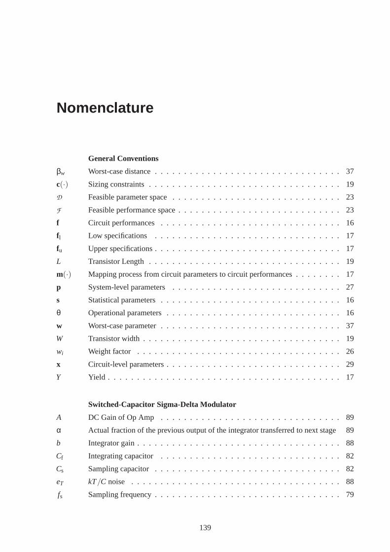
Nomenclature
General Conventions
βw Worst-case distance . . . . . . . . . . . . . . . . . . . . . . . . . . . . . . . . 37
c(·) Sizing constraints . . . . . . . . . . . . . . . . . . . . . . . . . . . . . . . . . 19
D Feasible parameter space . . . . . . . . . . . . . . . . . . . . . . . . . . . . .23
F Feasible performance space . . . . . . . . . . . . . . . . . . . . . . . . . . .. 23
f Circuit performances . . . . . . . . . . . . . . . . . . . . . . . . . . . . . . . 16
f l Low specifications . . . . . . . . . . . . . . . . . . . . . . . . . . . . . . . . 17
fu Upper specifications . . . . . . . . . . . . . . . . . . . . . . . . . . . . . . . . 17
L Transistor Length . . . . . . . . . . . . . . . . . . . . . . . . . . . . . . . . . 19
m(·) Mapping process from circuit parameters to circuit performances . . . . . . . . 17
p System-level parameters . . . . . . . . . . . . . . . . . . . . . . . . . . . . .27
s Statistical parameters . . . . . . . . . . . . . . . . . . . . . . . . . . . . . .. 16
θ Operational parameters . . . . . . . . . . . . . . . . . . . . . . . . . . . . . .16
w Worst-case parameter . . . . . . . . . . . . . . . . . . . . . . . . . . . . . . . 37
W Transistor width . . . . . . . . . . . . . . . . . . . . . . . . . . . . . . . . . . 19
wi Weight factor . . . . . . . . . . . . . . . . . . . . . . . . . . . . . . . . . . . 26
x Circuit-level parameters . . . . . . . . . . . . . . . . . . . . . . . . . . . .. . 29
Y Yield . . . . . . . . . . . . . . . . . . . . . . . . . . . . . . . . . . . . . . . . 17
Switched-Capacitor Sigma-Delta Modulator
A DC Gain of Op Amp . . . . . . . . . . . . . . . . . . . . . . . . . . . . . . . 89
α Actual fraction of the previous output of the integrator transferred to next stage 89
b Integrator gain . . . . . . . . . . . . . . . . . . . . . . . . . . . . . . . . . . . 88
Cf Integrating capacitor . . . . . . . . . . . . . . . . . . . . . . . . . . . . . . .82
Cs Sampling capacitor . . . . . . . . . . . . . . . . . . . . . . . . . . . . . . . . 82
eT kT/C noise . . . . . . . . . . . . . . . . . . . . . . . . . . . . . . . . . . . . 88
fs Sampling frequency . . . . . . . . . . . . . . . . . . . . . . . . . . . . . . . . 79
139

Nomenclature
GBW Unity-gain bandwidth of Op Amp . . . . . . . . . . . . . . . . . . . . . . . . 90
K Boltzmann’s constant . . . . . . . . . . . . . . . . . . . . . . . . . . . . . . . 88
N Conversion resolution . . . . . . . . . . . . . . . . . . . . . . . . . . . . . . .79
R Oversampling ration . . . . . . . . . . . . . . . . . . . . . . . . . . . . . . . . 79
RN(t) Gaussian random number with zero mean and unity standard deviation . . . . . 88
onT Finite resistance of switch . . . . . . . . . . . . . . . . . . . . . . . . . . .. . 88
SR Slew rate of Op Amp . . . . . . . . . . . . . . . . . . . . . . . . . . . . . . . 90
T Absolute temperature . . . . . . . . . . . . . . . . . . . . . . . . . . . . . . . 88
Ts Sampling period . . . . . . . . . . . . . . . . . . . . . . . . . . . . . . . . . . 109
Vn Total rms noise voltage of the operation amplifier . . . . . . . . .. . . . . . . 88
E(z) z-transform of the quantization noise . . . . . . . . . . . . . . . . . . .. . . . 83
NTF(z) z-transfer function of the quantization noise . . . . . . . . . . . .. . . . . . . 83
STF(z) z-transfer function of the input signal . . . . . . . . . . . . . . . . . .. . . . . 83
X(z) z-transform of the input signal . . . . . . . . . . . . . . . . . . . . . . . . .. 83
Y(z) z-transform of the out signal . . . . . . . . . . . . . . . . . . . . . . . . . . .83
Charge-Pump Phase-Locked Loop
C1 Capacitor 1 in Loop filter . . . . . . . . . . . . . . . . . . . . . . . . . . . . . 42
C2 Capacitor 2 in Loop filter . . . . . . . . . . . . . . . . . . . . . . . . . . . . . 42
f0 Carrier frequency in spectrum . . . . . . . . . . . . . . . . . . . . . . . . .. 50
∆ f Offset frequency from carrier frequency . . . . . . . . . . . . . . . .. . . . . 50
fmax Maximal output frequency . . . . . . . . . . . . . . . . . . . . . . . . . . . . 43
fmin Minimal output frequency . . . . . . . . . . . . . . . . . . . . . . . . . . . . .43
fout Output frequency . . . . . . . . . . . . . . . . . . . . . . . . . . . . . . . . . 40
fref Reference input frequency . . . . . . . . . . . . . . . . . . . . . . . . . . . .40
FLF(s) Transfer function of loop filter ins-domain . . . . . . . . . . . . . . . . . . . . 45
H(s) Closed loop transfer function ins-domain . . . . . . . . . . . . . . . . . . . . 45
H(z) Closed loop transfer function inz-domain . . . . . . . . . . . . . . . . . . . . 46
ICP Out-biased current of charge pump . . . . . . . . . . . . . . . . . . . . . .. . 42
Jcc cycle-to-cycle jitter . . . . . . . . . . . . . . . . . . . . . . . . . . . . . . .. 52
Jee edge-to-edge jitter . . . . . . . . . . . . . . . . . . . . . . . . . . . . . . . . .52
Jk long-term jitter . . . . . . . . . . . . . . . . . . . . . . . . . . . . . . . . . . 52
KVCO Gain of VCO in unit of Hz/V . . . . . . . . . . . . . . . . . . . . . . . . . . . 43
Kc Ratio ofC1 to C2 . . . . . . . . . . . . . . . . . . . . . . . . . . . . . . . . . 46
140

L(∆ f ) Phase noise on the offset frequency∆ f in unit of dBc/Hz . . . . . . . . . . . . 50
LG(s) Open loop transfer function ins-domain . . . . . . . . . . . . . . . . . . . . . 45
LG(z) Open loop transfer function inz-domain . . . . . . . . . . . . . . . . . . . . . 46
N Divider value . . . . . . . . . . . . . . . . . . . . . . . . . . . . . . . . . . . 40
φPM Phase margin . . . . . . . . . . . . . . . . . . . . . . . . . . . . . . . . . . . 54
φfb Phase of feedback signal . . . . . . . . . . . . . . . . . . . . . . . . . . . . . 40
φref Phase of input reference signal . . . . . . . . . . . . . . . . . . . . . . . .. . 40
R Resistor in Loop filter . . . . . . . . . . . . . . . . . . . . . . . . . . . . . . . 42
Sφ( f ) Noise power spectral density . . . . . . . . . . . . . . . . . . . . . . . . . .. 53
σ∆φ Phase jitter . . . . . . . . . . . . . . . . . . . . . . . . . . . . . . . . . . . . . 52
σ∆T Timing jitter . . . . . . . . . . . . . . . . . . . . . . . . . . . . . . . . . . . . 52
Ts Locking time . . . . . . . . . . . . . . . . . . . . . . . . . . . . . . . . . . . 49
vmax Maximal input voltage . . . . . . . . . . . . . . . . . . . . . . . . . . . . . . 43
vmin Minimal input voltage . . . . . . . . . . . . . . . . . . . . . . . . . . . . . . . 43
vc Voltage across the loop filter capacitorC1 . . . . . . . . . . . . . . . . . . . . 48
vctrl VCO control voltage . . . . . . . . . . . . . . . . . . . . . . . . . . . . . . . 48
ω1 Loop filter time constant 1 . . . . . . . . . . . . . . . . . . . . . . . . . . . . 46
ω2 Loop filter time constant 2 . . . . . . . . . . . . . . . . . . . . . . . . . . . . 46
ωp3 PLL’s third pole . . . . . . . . . . . . . . . . . . . . . . . . . . . . . . . . . . 54
ωUGB PLL’s Unity-gain bandwidth . . . . . . . . . . . . . . . . . . . . . . . . . . .54
ωz PLL’s zero . . . . . . . . . . . . . . . . . . . . . . . . . . . . . . . . . . . . . 54
ωi Reference input frequency . . . . . . . . . . . . . . . . . . . . . . . . . . . .46
141


List of Figures
1.1 Digital versus analog design in SoC [Cad02] . . . . . . . . . . .. . . . . . . . 2
1.2 Analog circuits in wireless communication system . . . . .. . . . . . . . . . . 3
1.3 (a) Two-stage OP AMP (b) its “thumbs models” [TMG02] . . . .. . . . . . . 5
1.4 Relative performance of analog and digital circuits over time [BM04] . . . . . 5
1.5 (a) Hierarchical design steps of analog/mixed-signal integrated circuit design(b) detailed design processes on an analog circuit . . . . . . . .. . . . . . . . 7
1.6 Knowledge-based optimization approaches . . . . . . . . . . .. . . . . . . . 10
1.7 "Simulation-in-a-loop"-based optimization approaches . . . . . . . . . . . . . 11
2.1 Schematic of a current-mode-logic(CML) cell . . . . . . . . .. . . . . . . . . 18
2.2 Simulation-based performance evaluation . . . . . . . . . . .. . . . . . . . . 19
2.3 Delay variation of CMLvs.process corners . . . . . . . . . . . . . . . . . . . 20
2.4 Yield estimation by means of MC analysis . . . . . . . . . . . . . .. . . . . . 21
2.5 Design flow of the automatic sizing process . . . . . . . . . . . .. . . . . . . 26
2.6 Feasible parameter spaceD . . . . . . . . . . . . . . . . . . . . . . . . . . . . 26
2.7 Feasible performance spaceF . . . . . . . . . . . . . . . . . . . . . . . . . . 27
2.8 Normal boundary intersection [SGA03] . . . . . . . . . . . . . . .. . . . . . 29
3.1 Step sizes in numerical simulation . . . . . . . . . . . . . . . . . .. . . . . . 32
3.2 Hierarchical sizing of a large-scale analog/mixed-signal circuit . . . . . . . . . 34
3.3 Pareto-optimal fronts in hierarchical optimization . .. . . . . . . . . . . . . . 35
3.4 (a) Basic structure of VHDL-AMS Model (b) A VHDL-AMS Model of an idealOP AMP with slew-rate limiting [APT02] . . . . . . . . . . . . . . . . . .. . 37
3.5 A simulink model for a real integrator [MBF+03] . . . . . . . . . . . . . . . . 38
3.6 Proposed hierarchical optimization design flow . . . . . . .. . . . . . . . . . 39
143

List of Figures
3.7 Transformation froms∼ N(s0,C) into s∼ N(0,1) . . . . . . . . . . . . . . . 41
3.8 Visualization of the worst-case analysis definition fora given robustnessβw . . 42
3.9 Worst-case analysis on nominal Pareto-optimal front . .. . . . . . . . . . . . 42
4.1 A block diagram for a typical PLL . . . . . . . . . . . . . . . . . . . . .. . . 44
4.2 Building blocks of a 3rd-order CPPLL . . . . . . . . . . . . . . . . . . . . . . 45
4.3 (a) State machine of a PFD (b) Clock diagram example . . . . .. . . . . . . . 45
4.4 A five-stage ring oscillator . . . . . . . . . . . . . . . . . . . . . . . .. . . . 47
4.5 Frequencyvs. input control voltage for an ideal VCO . . . . . . . . . . . . . . 47
4.6 Circuit diagram of a 1/4 divider . . . . . . . . . . . . . . . . . . . . .. . . . . 48
4.7 Linear model of a CPPLL . . . . . . . . . . . . . . . . . . . . . . . . . . . . .49
4.8 Discrete model of a CPPLL . . . . . . . . . . . . . . . . . . . . . . . . . . .. 50
4.9 (a) Definition of tp and T− (b) Two state-space variables in RC network[HBMM04] . . . . . . . . . . . . . . . . . . . . . . . . . . . . . . . . . . . . 52
4.10 Locking time definition . . . . . . . . . . . . . . . . . . . . . . . . . . .. . . 53
4.11 Oscillator power spectrum [Rob03] . . . . . . . . . . . . . . . . .. . . . . . . 54
4.12 A typical spectrum for signal-sideband phase noise [Rob03] . . . . . . . . . . 55
4.13 Jitter definition . . . . . . . . . . . . . . . . . . . . . . . . . . . . . . . .. . 55
4.14 Bode diagram for open loop of a third-order CPPLL . . . . . .. . . . . . . . . 58
4.15 CPPLL instability observed inz-domain analysis . . . . . . . . . . . . . . . . 59
4.16 Linear model of a CPPLL with noise sources . . . . . . . . . . . .. . . . . . 60
4.17 Loop transfer function from each noise source to PLL’s output . . . . . . . . . 62
4.18 Schematic of CP Block . . . . . . . . . . . . . . . . . . . . . . . . . . . . .. 63
4.19 Schematic of VCO Block . . . . . . . . . . . . . . . . . . . . . . . . . . . .. 64
4.20 Hierarchical performance modeling of the CPPLL . . . . . .. . . . . . . . . . 66
4.21 Pareto-optimal front of the CP . . . . . . . . . . . . . . . . . . . . .. . . . . 70
4.22 Pareto-optimal front of the VCO . . . . . . . . . . . . . . . . . . . .. . . . . 71
4.23 File system in WiCkeD . . . . . . . . . . . . . . . . . . . . . . . . . . . . .. 72
4.24 Pareto-optimal front of the CP . . . . . . . . . . . . . . . . . . . . .. . . . . 75
4.25 (a) 3D Pareto-optimal front of the VCO (b) Contours of jitter in 2D surface(gain vs. current) . . . . . . . . . . . . . . . . . . . . . . . . . . . . . . . . . 75
4.26 Pareto-optimal front of jitter and locking time at input jitter=1ns . . . . . . . . 76
144

List of Figures
4.27 Pareto-optimal front of jitter and locking time at input jitter=0 and settingICP=Imax . . . . . . . . . . . . . . . . . . . . . . . . . . . . . . . . . . . . . . . . 77
5.1 Block diagram of A/D Converters and Noise spectrum . . . . .. . . . . . . . 83
5.2 A second-order SCΣ∆ modulator [BW88] . . . . . . . . . . . . . . . . . . . . 86
5.3 Single-ended SC Integrator . . . . . . . . . . . . . . . . . . . . . . . .. . . . 87
5.4 Linear model of the modulator with an injected quantization noise . . . . . . . 88
5.5 Ideal linear Model of the 2nd-order SCΣ∆ modulator . . . . . . . . . . . . . . 89
5.6 PSD plot of the ideal 2nd-order SCΣ∆ modulator @ OSR=256: . . . . . . . . 89
5.7 SNR vs. OSR in the ideal 2nd-order SCΣ∆ modulator . . . . . . . . . . . . . 90
5.8 Clock jitter on sampling input signal . . . . . . . . . . . . . . . .. . . . . . . 91
5.9 Effect of clock jitter . . . . . . . . . . . . . . . . . . . . . . . . . . . . .. . . 92
5.10 Equivalent SC circuits in (a)φ1 (b) φ2 . . . . . . . . . . . . . . . . . . . . . . 92
5.11 Effect of noise . . . . . . . . . . . . . . . . . . . . . . . . . . . . . . . . . .. 93
5.12 Integrator output response . . . . . . . . . . . . . . . . . . . . . . .. . . . . 95
5.13 Effects of non-identities in OP AMP . . . . . . . . . . . . . . . . .. . . . . . 97
5.14 A second-order SCΣ∆ modulator model in Simulink . . . . . . . . . . . . . . 98
5.15 Hierarchical performance modeling of the SCΣ∆ modulator . . . . . . . . . . 99
5.16 Schematic of a fold cascode OP AMP . . . . . . . . . . . . . . . . . . .. . . 99
5.17 angle=90 . . . . . . . . . . . . . . . . . . . . . . . . . . . . . . . . . . . . . 101
5.18 SNR vs Parameter Sweep . . . . . . . . . . . . . . . . . . . . . . . . . . . .. 102
5.19 Pareto-optimal front of GBW vs. SR . . . . . . . . . . . . . . . . . .. . . . . 103
B.1 Modeling a random sampling jitter [MBF+03] . . . . . . . . . . . . . . . . . . 113
B.2 Modeling switches thermal noiseKT/C block [MBF+03] . . . . . . . . . . . . 114
B.3 Modeling operational amplifier noise [MBF+03] . . . . . . . . . . . . . . . . 114
B.4 Modeling real integrator [MBF+03] . . . . . . . . . . . . . . . . . . . . . . . 115
145

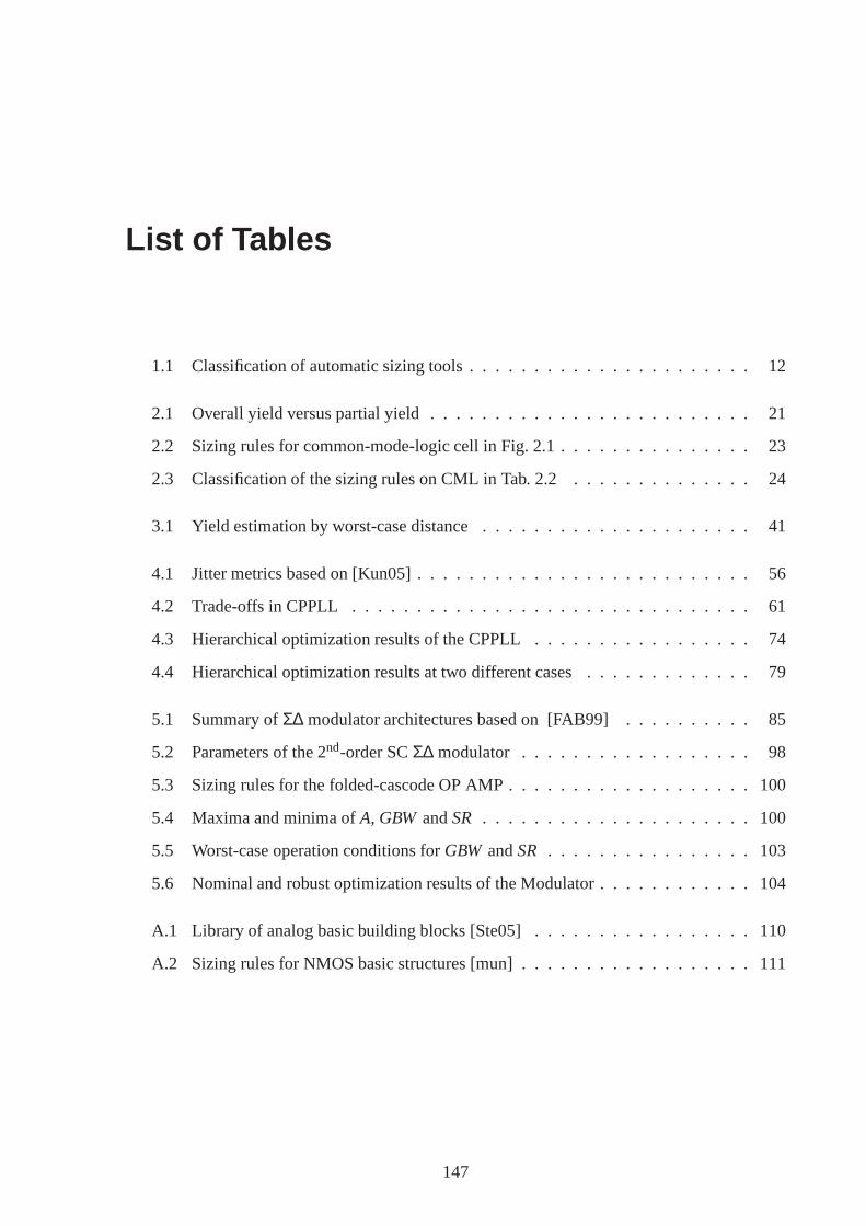
List of Tables
1.1 Classification of automatic sizing tools . . . . . . . . . . . . .. . . . . . . . . 12
2.1 Overall yield versus partial yield . . . . . . . . . . . . . . . . . .. . . . . . . 21
2.2 Sizing rules for common-mode-logic cell in Fig. 2.1 . . . .. . . . . . . . . . . 23
2.3 Classification of the sizing rules on CML in Tab. 2.2 . . . . .. . . . . . . . . 24
3.1 Yield estimation by worst-case distance . . . . . . . . . . . . .. . . . . . . . 41
4.1 Jitter metrics based on [Kun05] . . . . . . . . . . . . . . . . . . . . .. . . . . 56
4.2 Trade-offs in CPPLL . . . . . . . . . . . . . . . . . . . . . . . . . . . . . . .61
4.3 Hierarchical optimization results of the CPPLL . . . . . . .. . . . . . . . . . 74
4.4 Hierarchical optimization results at two different cases . . . . . . . . . . . . . 79
5.1 Summary ofΣ∆ modulator architectures based on [FAB99] . . . . . . . . . . 85
5.2 Parameters of the 2nd-order SCΣ∆ modulator . . . . . . . . . . . . . . . . . . 98
5.3 Sizing rules for the folded-cascode OP AMP . . . . . . . . . . . .. . . . . . . 100
5.4 Maxima and minima ofA, GBW andSR . . . . . . . . . . . . . . . . . . . . . 100
5.5 Worst-case operation conditions forGBW andSR . . . . . . . . . . . . . . . . 103
5.6 Nominal and robust optimization results of the Modulator . . . . . . . . . . . . 104
A.1 Library of analog basic building blocks [Ste05] . . . . . . .. . . . . . . . . . 110
A.2 Sizing rules for NMOS basic structures [mun] . . . . . . . . . .. . . . . . . . 111
147


Abstract in German
Die vorliegende Arbeit stellt ein automatisiertes hierarchisches Dimensionierungsverfahren fürkomplexe Analog-/Mixed-Signal-Schaltungen vor. Es wird von einem Systemmodell auf derVerhaltensebene und einer Modellierung der Systemblöcke auf der Transistorebene ausge-gangen. Bei dem vorgeschlagenen zweistufigen Dimensionierungsprozess werden zunächstSystemparameter dimensioniert und als Spezifikation an dienachfolgende Transistordimen-sionierung der Systemblöcke weitergereicht. Durch eine Vorab-Charakterisierung des Eigen-schaftspotentials der Systemblöcke mittels Pareto-Optimierung wird eine realistische Systemdi-mensionierung sichergestellt und so ein iterationsfreierTop-Down-Entwurfsprozess erzeugt.Das vorgestellte Verfahren wird anhand des Entwurfs von Phasenregelschleifen und Sigma-Delta-Modulatoren demonstriert.
149
