high dynamic range cmos sensor - bdticpreliminary data this is preliminary information on a new...
TRANSCRIPT

Preliminary data
This is preliminary information on a new product now in development or undergoing evaluation. Details are subject to change without notice.
May 2009 8193589 Rev A 1/119
1
VL5510
High dynamic range CMOS sensor
Features■ 1024 x 512 monochrome resolution sensor
■ High dynamic pixel (5.6 µm x 5.6 µm)
■ Parallel video data output interface (12-bit parallel interface)
■ High speed serial link (CCP interface)
■ I2C control interface
■ SPI slave control interface
■ UART control interface
■ SPI master interface
■ 3.3 V operation, 2.5 V for LVDS pads power supply
■ On-board 12-bit ADC
■ Small physical size
■ Ultra low power standby mode
■ On-chip PLL
■ 34 fps maximum frame rate at full resolution
■ On-chip anti dark sun correction
■ On-chip VFPN correction (CDS)
■ On-chip defect correction
■ On-chip microcontroller for system level flexibility
Applications■ Adaptive cruise control/stop and go
■ Pedestrian detection and protection
■ Headway/forward collision warning
■ Pre-crash active safety
■ Lane departure warning
■ Lane keeping
■ Night vision (NIR - Near InfraRed)
■ Automatic high/low beam control
■ Lane change assist
■ Blind spot detection
Table 1. Device summary
Root part number Package Packing
VL5510Bare die Tray
OLGA UNSAW DICE
Bare Die
www.st.com
www.bdtic.com/ST

Contents VL5510
2/119 8193589 Rev A
Contents
1 Overview . . . . . . . . . . . . . . . . . . . . . . . . . . . . . . . . . . . . . . . . . . . . . . . . . . 8
1.1 Technical specification . . . . . . . . . . . . . . . . . . . . . . . . . . . . . . . . . . . . . . . . 8
1.2 Description . . . . . . . . . . . . . . . . . . . . . . . . . . . . . . . . . . . . . . . . . . . . . . . . . 9
1.3 Signal description . . . . . . . . . . . . . . . . . . . . . . . . . . . . . . . . . . . . . . . . . . . 10
1.4 Bare die . . . . . . . . . . . . . . . . . . . . . . . . . . . . . . . . . . . . . . . . . . . . . . . . . . 13
1.4.1 Die size . . . . . . . . . . . . . . . . . . . . . . . . . . . . . . . . . . . . . . . . . . . . . . . . . 13
1.4.2 Pad placement . . . . . . . . . . . . . . . . . . . . . . . . . . . . . . . . . . . . . . . . . . . . 14
1.4.3 Pad coordinates . . . . . . . . . . . . . . . . . . . . . . . . . . . . . . . . . . . . . . . . . . . 15
2 Functional description . . . . . . . . . . . . . . . . . . . . . . . . . . . . . . . . . . . . . . 19
2.1 Operation . . . . . . . . . . . . . . . . . . . . . . . . . . . . . . . . . . . . . . . . . . . . . . . . . 20
2.2 System clocking . . . . . . . . . . . . . . . . . . . . . . . . . . . . . . . . . . . . . . . . . . . . 21
2.3 Imager control block (ICB) . . . . . . . . . . . . . . . . . . . . . . . . . . . . . . . . . . . . 21
2.3.1 I2C slave interface (V2W) . . . . . . . . . . . . . . . . . . . . . . . . . . . . . . . . . . . . 21
2.3.2 SPI slave and UART interfaces . . . . . . . . . . . . . . . . . . . . . . . . . . . . . . . 24
2.3.3 SPI master interface . . . . . . . . . . . . . . . . . . . . . . . . . . . . . . . . . . . . . . . 26
2.4 Image digital pipeline (IDP) . . . . . . . . . . . . . . . . . . . . . . . . . . . . . . . . . . . 27
2.4.1 Video timing controller . . . . . . . . . . . . . . . . . . . . . . . . . . . . . . . . . . . . . . 27
2.4.2 Antidark sun correction . . . . . . . . . . . . . . . . . . . . . . . . . . . . . . . . . . . . . 28
2.4.3 Test pattern generation . . . . . . . . . . . . . . . . . . . . . . . . . . . . . . . . . . . . . 28
2.4.4 Dark offset cancellation . . . . . . . . . . . . . . . . . . . . . . . . . . . . . . . . . . . . . 29
2.4.5 Channel gain . . . . . . . . . . . . . . . . . . . . . . . . . . . . . . . . . . . . . . . . . . . . . 30
2.4.6 Channel offset . . . . . . . . . . . . . . . . . . . . . . . . . . . . . . . . . . . . . . . . . . . . 30
2.4.7 Vertical fixed pattern noise (VFPN) correction . . . . . . . . . . . . . . . . . . . . 30
2.4.8 Defect correction . . . . . . . . . . . . . . . . . . . . . . . . . . . . . . . . . . . . . . . . . . 31
2.4.9 Crop . . . . . . . . . . . . . . . . . . . . . . . . . . . . . . . . . . . . . . . . . . . . . . . . . . . . 31
2.4.10 Statistic engine . . . . . . . . . . . . . . . . . . . . . . . . . . . . . . . . . . . . . . . . . . . 33
2.4.11 Status line coder . . . . . . . . . . . . . . . . . . . . . . . . . . . . . . . . . . . . . . . . . . 34
2.4.12 Trailer . . . . . . . . . . . . . . . . . . . . . . . . . . . . . . . . . . . . . . . . . . . . . . . . . . . 34
2.4.13 Parallel 12-bit video interface . . . . . . . . . . . . . . . . . . . . . . . . . . . . . . . . . 35
2.4.14 CCP Tx coder . . . . . . . . . . . . . . . . . . . . . . . . . . . . . . . . . . . . . . . . . . . . 35
2.5 Imaging array - CAB frame format . . . . . . . . . . . . . . . . . . . . . . . . . . . . . . 39
2.6 Parallel interface frame format . . . . . . . . . . . . . . . . . . . . . . . . . . . . . . . . . 40
www.bdtic.com/ST

VL5510 Contents
8193589 Rev A 3/119
2.7 CCP Tx frame format . . . . . . . . . . . . . . . . . . . . . . . . . . . . . . . . . . . . . . . . 41
2.8 Sensor operating modes . . . . . . . . . . . . . . . . . . . . . . . . . . . . . . . . . . . . . 42
2.8.1 Low power state . . . . . . . . . . . . . . . . . . . . . . . . . . . . . . . . . . . . . . . . . . . 42
2.8.2 Standby state . . . . . . . . . . . . . . . . . . . . . . . . . . . . . . . . . . . . . . . . . . . . . 42
2.8.3 Streaming state . . . . . . . . . . . . . . . . . . . . . . . . . . . . . . . . . . . . . . . . . . . 42
2.8.4 Static parameter changes . . . . . . . . . . . . . . . . . . . . . . . . . . . . . . . . . . . 42
3 Operation mode . . . . . . . . . . . . . . . . . . . . . . . . . . . . . . . . . . . . . . . . . . . . 43
3.1 Mode definitions . . . . . . . . . . . . . . . . . . . . . . . . . . . . . . . . . . . . . . . . . . . . 43
4 High dynamic mode . . . . . . . . . . . . . . . . . . . . . . . . . . . . . . . . . . . . . . . . 44
4.1 Linear pixel response . . . . . . . . . . . . . . . . . . . . . . . . . . . . . . . . . . . . . . . . 44
4.2 High dynamic pixel response . . . . . . . . . . . . . . . . . . . . . . . . . . . . . . . . . . 45
5 Programming model . . . . . . . . . . . . . . . . . . . . . . . . . . . . . . . . . . . . . . . . 47
6 Register description . . . . . . . . . . . . . . . . . . . . . . . . . . . . . . . . . . . . . . . . 48
6.1 Register type . . . . . . . . . . . . . . . . . . . . . . . . . . . . . . . . . . . . . . . . . . . . . . 48
6.2 User interface map . . . . . . . . . . . . . . . . . . . . . . . . . . . . . . . . . . . . . . . . . . 48
6.2.1 DeviceParameters [read only] . . . . . . . . . . . . . . . . . . . . . . . . . . . . . . . . 48
6.2.2 PrivateSetupUpdate . . . . . . . . . . . . . . . . . . . . . . . . . . . . . . . . . . . . . . . . 48
6.2.3 PrivateModeDin . . . . . . . . . . . . . . . . . . . . . . . . . . . . . . . . . . . . . . . . . . . 48
6.2.4 IcbSetupModeSelect . . . . . . . . . . . . . . . . . . . . . . . . . . . . . . . . . . . . . . . 49
6.2.5 IcbSetupSoftwareReset . . . . . . . . . . . . . . . . . . . . . . . . . . . . . . . . . . . . . 49
6.2.6 PrePllClkDiv . . . . . . . . . . . . . . . . . . . . . . . . . . . . . . . . . . . . . . . . . . . . . . 49
6.2.7 PllMultiplier . . . . . . . . . . . . . . . . . . . . . . . . . . . . . . . . . . . . . . . . . . . . . . 49
6.3 Register map . . . . . . . . . . . . . . . . . . . . . . . . . . . . . . . . . . . . . . . . . . . . . . 50
6.3.1 Multi-byte register index space . . . . . . . . . . . . . . . . . . . . . . . . . . . . . . . 51
6.3.2 Data alignment within registers . . . . . . . . . . . . . . . . . . . . . . . . . . . . . . . 52
6.3.3 Valid register data types . . . . . . . . . . . . . . . . . . . . . . . . . . . . . . . . . . . . 52
6.3.4 Status registers [0x0000 to 0x000F] . . . . . . . . . . . . . . . . . . . . . . . . . . . 53
6.3.5 Frame format description registers [0x0040 to 0x007F] . . . . . . . . . . . . 54
6.3.6 Setup registers [0x0100 to 0x01FF] . . . . . . . . . . . . . . . . . . . . . . . . . . . . 56
6.3.7 Integration time and gain registers [0x0200 to 0x02FF] . . . . . . . . . . . . . 58
6.3.8 Video timing registers [0x0300 to 0x03FF] . . . . . . . . . . . . . . . . . . . . . . 60
6.3.9 Test pattern registers [0x0600 to 0x06FF] . . . . . . . . . . . . . . . . . . . . . . . 71
6.3.10 Manufacturer specific registers [0x3000 to 0x34FF] . . . . . . . . . . . . . . . 72
www.bdtic.com/ST

Contents VL5510
4/119 8193589 Rev A
6.3.11 Firmware registers . . . . . . . . . . . . . . . . . . . . . . . . . . . . . . . . . . . . . . . . . 87
6.3.12 Private registers [0x3800 to 0xFFF4] . . . . . . . . . . . . . . . . . . . . . . . . . . . 91
6.3.13 Trailer content information . . . . . . . . . . . . . . . . . . . . . . . . . . . . . . . . . . . 93
7 Electrical characteristics . . . . . . . . . . . . . . . . . . . . . . . . . . . . . . . . . . . 107
7.1 Operational envelope . . . . . . . . . . . . . . . . . . . . . . . . . . . . . . . . . . . . . . . 107
7.1.1 Absolute maximum ratings . . . . . . . . . . . . . . . . . . . . . . . . . . . . . . . . . . 107
7.1.2 Normal operation . . . . . . . . . . . . . . . . . . . . . . . . . . . . . . . . . . . . . . . . . 107
7.2 Electrostatic discharge voltage (ESD) . . . . . . . . . . . . . . . . . . . . . . . . . . 107
7.3 AC electrical characteristics . . . . . . . . . . . . . . . . . . . . . . . . . . . . . . . . . . 108
7.3.1 External clock . . . . . . . . . . . . . . . . . . . . . . . . . . . . . . . . . . . . . . . . . . . 108
7.3.2 Chip enable (CE) . . . . . . . . . . . . . . . . . . . . . . . . . . . . . . . . . . . . . . . . . 109
7.3.3 I2C slave interface . . . . . . . . . . . . . . . . . . . . . . . . . . . . . . . . . . . . . . . . 109
7.3.4 Parallel data interface timings . . . . . . . . . . . . . . . . . . . . . . . . . . . . . . . 112
7.3.5 CCP Tx interface timing . . . . . . . . . . . . . . . . . . . . . . . . . . . . . . . . . . . . 113
8 Package characteristics . . . . . . . . . . . . . . . . . . . . . . . . . . . . . . . . . . . . 114
8.1 Lead-free packages . . . . . . . . . . . . . . . . . . . . . . . . . . . . . . . . . . . . . . . . 114
8.2 Ordering information . . . . . . . . . . . . . . . . . . . . . . . . . . . . . . . . . . . . . . . 114
8.3 OLGA package . . . . . . . . . . . . . . . . . . . . . . . . . . . . . . . . . . . . . . . . . . . . 114
9 Revision history . . . . . . . . . . . . . . . . . . . . . . . . . . . . . . . . . . . . . . . . . . 118
www.bdtic.com/ST

VL5510 List of tables
8193589 Rev A 5/119
List of tables
Table 1. Device summary . . . . . . . . . . . . . . . . . . . . . . . . . . . . . . . . . . . . . . . . . . . . . . . . . . . . . . . . . . 1Table 2. Technical specification . . . . . . . . . . . . . . . . . . . . . . . . . . . . . . . . . . . . . . . . . . . . . . . . . . . . . 8Table 3. VL5510 signal description. . . . . . . . . . . . . . . . . . . . . . . . . . . . . . . . . . . . . . . . . . . . . . . . . . 10Table 4. Central X and Y pad coordinates for wire bonding . . . . . . . . . . . . . . . . . . . . . . . . . . . . . . . 15Table 5. VL5510 mode definitions . . . . . . . . . . . . . . . . . . . . . . . . . . . . . . . . . . . . . . . . . . . . . . . . . . 43Table 6. DeviceParameters . . . . . . . . . . . . . . . . . . . . . . . . . . . . . . . . . . . . . . . . . . . . . . . . . . . . . . . 48Table 7. PrivateSetupUpdate . . . . . . . . . . . . . . . . . . . . . . . . . . . . . . . . . . . . . . . . . . . . . . . . . . . . . . 48Table 8. PrivateModeDin . . . . . . . . . . . . . . . . . . . . . . . . . . . . . . . . . . . . . . . . . . . . . . . . . . . . . . . . . 48Table 9. IcbSetupModeSelect. . . . . . . . . . . . . . . . . . . . . . . . . . . . . . . . . . . . . . . . . . . . . . . . . . . . . . 49Table 10. IcbSetupSoftwareReset . . . . . . . . . . . . . . . . . . . . . . . . . . . . . . . . . . . . . . . . . . . . . . . . . . . 49Table 11. PrePllClkDiv . . . . . . . . . . . . . . . . . . . . . . . . . . . . . . . . . . . . . . . . . . . . . . . . . . . . . . . . . . . . 49Table 12. PllMultiplier . . . . . . . . . . . . . . . . . . . . . . . . . . . . . . . . . . . . . . . . . . . . . . . . . . . . . . . . . . . . . 49Table 13. Register map . . . . . . . . . . . . . . . . . . . . . . . . . . . . . . . . . . . . . . . . . . . . . . . . . . . . . . . . . . . 50Table 14. Valid 16-bit indices for the MS data byte of 16-bit wide register . . . . . . . . . . . . . . . . . . . . . 51Table 15. Valid 16-bit indices for the MS and LS data bytes of 32-bit wide registers . . . . . . . . . . . . . 51Table 16. Valid register data types . . . . . . . . . . . . . . . . . . . . . . . . . . . . . . . . . . . . . . . . . . . . . . . . . . . 52Table 17. Status registers [0x0000 to 0x000F] . . . . . . . . . . . . . . . . . . . . . . . . . . . . . . . . . . . . . . . . . . 53Table 18. Frame format description registers [0x0040 to 0x007F] . . . . . . . . . . . . . . . . . . . . . . . . . . . 54Table 19. Pixel data code . . . . . . . . . . . . . . . . . . . . . . . . . . . . . . . . . . . . . . . . . . . . . . . . . . . . . . . . . . 56Table 20. Setup registers [0x0100 to 0x01FF] . . . . . . . . . . . . . . . . . . . . . . . . . . . . . . . . . . . . . . . . . . 56Table 21. Integration time and gain registers [0x0200 - 0x02FF] . . . . . . . . . . . . . . . . . . . . . . . . . . . . 58Table 22. Analog gain ranges. . . . . . . . . . . . . . . . . . . . . . . . . . . . . . . . . . . . . . . . . . . . . . . . . . . . . . . 59Table 23. Video timing registers [0x0300 to 0x03FF] . . . . . . . . . . . . . . . . . . . . . . . . . . . . . . . . . . . . . 60Table 24. Test pattern registers [0x0600 to 0x06FF] . . . . . . . . . . . . . . . . . . . . . . . . . . . . . . . . . . . . . 71Table 25. Manufacturer specific registers [0x3000 to 0x34FF] . . . . . . . . . . . . . . . . . . . . . . . . . . . . . . 72Table 26. Firmware registers . . . . . . . . . . . . . . . . . . . . . . . . . . . . . . . . . . . . . . . . . . . . . . . . . . . . . . . 87Table 27. Private registers [0x3800 to 0xFFF4] . . . . . . . . . . . . . . . . . . . . . . . . . . . . . . . . . . . . . . . . . 91Table 28. Trailer content information . . . . . . . . . . . . . . . . . . . . . . . . . . . . . . . . . . . . . . . . . . . . . . . . . 94Table 29. Maximum ratings . . . . . . . . . . . . . . . . . . . . . . . . . . . . . . . . . . . . . . . . . . . . . . . . . . . . . . . 107Table 30. Supply specification . . . . . . . . . . . . . . . . . . . . . . . . . . . . . . . . . . . . . . . . . . . . . . . . . . . . . 107Table 31. Clock input signal specification. . . . . . . . . . . . . . . . . . . . . . . . . . . . . . . . . . . . . . . . . . . . . 109Table 32. Serial interface voltage levels . . . . . . . . . . . . . . . . . . . . . . . . . . . . . . . . . . . . . . . . . . . . . . 109Table 33. Timing specification . . . . . . . . . . . . . . . . . . . . . . . . . . . . . . . . . . . . . . . . . . . . . . . . . . . . . 110Table 34. Parallel data interface timings. . . . . . . . . . . . . . . . . . . . . . . . . . . . . . . . . . . . . . . . . . . . . . 112Table 35. CCP interface - DATA+, DATA-, CLK+, CLK- characteristics. . . . . . . . . . . . . . . . . . . . . . 113Table 36. CCP interface timing characteristics . . . . . . . . . . . . . . . . . . . . . . . . . . . . . . . . . . . . . . . . . 113Table 37. Ordering information . . . . . . . . . . . . . . . . . . . . . . . . . . . . . . . . . . . . . . . . . . . . . . . . . . . . . 114Table 38. OLGA pinout . . . . . . . . . . . . . . . . . . . . . . . . . . . . . . . . . . . . . . . . . . . . . . . . . . . . . . . . . . . 115Table 39. Document revision history . . . . . . . . . . . . . . . . . . . . . . . . . . . . . . . . . . . . . . . . . . . . . . . . 118
www.bdtic.com/ST

List of figures VL5510
6/119 8193589 Rev A
List of figures
Figure 1. Die size . . . . . . . . . . . . . . . . . . . . . . . . . . . . . . . . . . . . . . . . . . . . . . . . . . . . . . . . . . . . . . . . 13Figure 2. Pad placement . . . . . . . . . . . . . . . . . . . . . . . . . . . . . . . . . . . . . . . . . . . . . . . . . . . . . . . . . . 14Figure 3. VL5510 block diagram . . . . . . . . . . . . . . . . . . . . . . . . . . . . . . . . . . . . . . . . . . . . . . . . . . . . 20Figure 4. I2C data transfer protocol . . . . . . . . . . . . . . . . . . . . . . . . . . . . . . . . . . . . . . . . . . . . . . . . . . 21Figure 5. I2C device address . . . . . . . . . . . . . . . . . . . . . . . . . . . . . . . . . . . . . . . . . . . . . . . . . . . . . . . 22Figure 6. I2C data format (write) . . . . . . . . . . . . . . . . . . . . . . . . . . . . . . . . . . . . . . . . . . . . . . . . . . . . 22Figure 7. I2C data format (read) . . . . . . . . . . . . . . . . . . . . . . . . . . . . . . . . . . . . . . . . . . . . . . . . . . . . . 23Figure 8. I2C data format (sequential write) . . . . . . . . . . . . . . . . . . . . . . . . . . . . . . . . . . . . . . . . . . . . 23Figure 9. I2C data format (sequential read) . . . . . . . . . . . . . . . . . . . . . . . . . . . . . . . . . . . . . . . . . . . . 23Figure 10. SPI slave interface - protocol . . . . . . . . . . . . . . . . . . . . . . . . . . . . . . . . . . . . . . . . . . . . . . . 24Figure 11. SPI slave interface - write transaction . . . . . . . . . . . . . . . . . . . . . . . . . . . . . . . . . . . . . . . . 25Figure 12. SPI slave interface - read transaction. . . . . . . . . . . . . . . . . . . . . . . . . . . . . . . . . . . . . . . . . 25Figure 13. UART interface - protocol . . . . . . . . . . . . . . . . . . . . . . . . . . . . . . . . . . . . . . . . . . . . . . . . . . 26Figure 14. VL5510 imaging pipe block diagram. . . . . . . . . . . . . . . . . . . . . . . . . . . . . . . . . . . . . . . . . . 27Figure 15. Video timing block schema . . . . . . . . . . . . . . . . . . . . . . . . . . . . . . . . . . . . . . . . . . . . . . . . . 27Figure 16. Fixed video pattern . . . . . . . . . . . . . . . . . . . . . . . . . . . . . . . . . . . . . . . . . . . . . . . . . . . . . . . 28Figure 17. Role of dark offset calibration . . . . . . . . . . . . . . . . . . . . . . . . . . . . . . . . . . . . . . . . . . . . . . . 29Figure 18. Statistic engine module diagram overview . . . . . . . . . . . . . . . . . . . . . . . . . . . . . . . . . . . . . 33Figure 19. Histogram window . . . . . . . . . . . . . . . . . . . . . . . . . . . . . . . . . . . . . . . . . . . . . . . . . . . . . . . 34Figure 20. Trailer diagram . . . . . . . . . . . . . . . . . . . . . . . . . . . . . . . . . . . . . . . . . . . . . . . . . . . . . . . . . . 34Figure 21. RAW8 data format in VGA case . . . . . . . . . . . . . . . . . . . . . . . . . . . . . . . . . . . . . . . . . . . . . 35Figure 22. RAW8 data transmission on CCP2 bus, bitwise illustration . . . . . . . . . . . . . . . . . . . . . . . . 36Figure 23. RAW8 frame format in VGA case . . . . . . . . . . . . . . . . . . . . . . . . . . . . . . . . . . . . . . . . . . . . 36Figure 24. RAW10 data format in VGA case . . . . . . . . . . . . . . . . . . . . . . . . . . . . . . . . . . . . . . . . . . . . 37Figure 25. RAW10 data transmission on CCP2 bus, bitwise illustration . . . . . . . . . . . . . . . . . . . . . . . 37Figure 26. RAW10 frame format in VGA case . . . . . . . . . . . . . . . . . . . . . . . . . . . . . . . . . . . . . . . . . . . 37Figure 27. RAW12 data format in VGA case . . . . . . . . . . . . . . . . . . . . . . . . . . . . . . . . . . . . . . . . . . . . 37Figure 28. RAW12 transmission on CCP2 bus, bitwise illustration . . . . . . . . . . . . . . . . . . . . . . . . . . . 38Figure 29. RAW12 frame format in VGA case . . . . . . . . . . . . . . . . . . . . . . . . . . . . . . . . . . . . . . . . . . . 38Figure 30. CAB frame format . . . . . . . . . . . . . . . . . . . . . . . . . . . . . . . . . . . . . . . . . . . . . . . . . . . . . . . . 39Figure 31. Parallel interface output frame format. . . . . . . . . . . . . . . . . . . . . . . . . . . . . . . . . . . . . . . . . 40Figure 32. CCP interface frame format . . . . . . . . . . . . . . . . . . . . . . . . . . . . . . . . . . . . . . . . . . . . . . . . 41Figure 33. VL5510 system state diagram . . . . . . . . . . . . . . . . . . . . . . . . . . . . . . . . . . . . . . . . . . . . . . 42Figure 34. Linear pixel response curves . . . . . . . . . . . . . . . . . . . . . . . . . . . . . . . . . . . . . . . . . . . . . . . 44Figure 35. Typical response. . . . . . . . . . . . . . . . . . . . . . . . . . . . . . . . . . . . . . . . . . . . . . . . . . . . . . . . . 45Figure 36. Pixel response with a dynamic range compression . . . . . . . . . . . . . . . . . . . . . . . . . . . . . . 45Figure 37. High dynamic range typical response. . . . . . . . . . . . . . . . . . . . . . . . . . . . . . . . . . . . . . . . . 46Figure 38. High dynamic pixel response . . . . . . . . . . . . . . . . . . . . . . . . . . . . . . . . . . . . . . . . . . . . . . . 46Figure 39. VL5510 addressable register/memory space . . . . . . . . . . . . . . . . . . . . . . . . . . . . . . . . . . . 47Figure 40. Right alignment for packing 10-bit data into two 8-bit registers . . . . . . . . . . . . . . . . . . . . . 52Figure 41. Frame format . . . . . . . . . . . . . . . . . . . . . . . . . . . . . . . . . . . . . . . . . . . . . . . . . . . . . . . . . . . 54Figure 42. 2-byte generic field format descriptor . . . . . . . . . . . . . . . . . . . . . . . . . . . . . . . . . . . . . . . . . 55Figure 43. Analog gain bits . . . . . . . . . . . . . . . . . . . . . . . . . . . . . . . . . . . . . . . . . . . . . . . . . . . . . . . . . 59Figure 44. External crystal oscillator . . . . . . . . . . . . . . . . . . . . . . . . . . . . . . . . . . . . . . . . . . . . . . . . . 108Figure 45. DC-coupled squarewave . . . . . . . . . . . . . . . . . . . . . . . . . . . . . . . . . . . . . . . . . . . . . . . . . 108Figure 46. AC-coupled sinewave . . . . . . . . . . . . . . . . . . . . . . . . . . . . . . . . . . . . . . . . . . . . . . . . . . . . 109Figure 47. Voltage level specification . . . . . . . . . . . . . . . . . . . . . . . . . . . . . . . . . . . . . . . . . . . . . . . . 110Figure 48. Timing specification . . . . . . . . . . . . . . . . . . . . . . . . . . . . . . . . . . . . . . . . . . . . . . . . . . . . . 111
www.bdtic.com/ST
VL5510 List of figures
8193589 Rev A 7/119
Figure 49. SDA/SCL rise and fall times . . . . . . . . . . . . . . . . . . . . . . . . . . . . . . . . . . . . . . . . . . . . . . . 112Figure 50. Parallel data output video timing. . . . . . . . . . . . . . . . . . . . . . . . . . . . . . . . . . . . . . . . . . . . 112Figure 51. OLGA package pinout . . . . . . . . . . . . . . . . . . . . . . . . . . . . . . . . . . . . . . . . . . . . . . . . . . . 115Figure 52. OLGA 80-pin lead pitch package outline and mechanical data . . . . . . . . . . . . . . . . . . . . 117
www.bdtic.com/ST

Overview VL5510
8/119 8193589 Rev A
1 Overview
1.1 Technical specification
Table 2. Technical specification
Feature Specification
Pixel resolution 1024 x 512
Sensor technology 0.13 µm 4 layers metal
Pixel size 5.6 µm x 5.6 µm
Characteristic line 10 knee points
Analog gain +24 dB (max)
Dynamic range (in scene) 120 dB
Dynamic range (overall) 140 dB
Signal to noise 42 dB (@ 1 lux)
Sensitivity 8.3 V/Lux.s
Pixel fill factor 60%
Remaining fixed pattern noise (FPN) < 0.1%
Temporal noise < 0.1%
Image lag < 0.1%
PRNU (Photo Response Non Uniformity) < 1%
Shutter Electrical rolling
Supply voltage3.3 V (±10%) supply2.5 V (±10%) LVDS I/O supply
Power consumption< 150 mW @ 34 fps< 15 µW (standby mode)
Temperature range-40 °C to + 125 °CDevice functional @ 85 °C max
Package Bare die/OLGA
www.bdtic.com/ST

VL5510 Overview
8193589 Rev A 9/119
1.2 DescriptionThe VL5510 is a 0.13 µm CMOS digital camera featuring a high dynamic range (1024 x 512 resolution) for automotive applications. This complete camera module is ready to connect to the camera enabled baseband processor.
Video data is output from the VL5510 over a 12-bit parallel interface and a high speed serial link (8/10/12 bits raw data output format supported on the compact camera port (CCP) interface compatible with an SMIA (standard mobile imaging architecture) normative.
Control interface is an SPI (serial peripheral interface) or UART (universal asynchronous receiver transmitter) interface or I2C (Inter Integrated Circuit) interface.
Power supplies delivered to the sensor are:
● 3.3 V for the analog blocks
● 3.3 V for the digital interface
● 2.5 V for the high speed serial link interface
● 1.2 V for the internal digital core (generated internally using a low drop output regulator)
The VL5510 is designed to operate in conjunction with an electronic central unit (ECU) that manages the device in the car.
An input clock is required in the range 6 MHz to 27.77 MHz.
The device contains an embedded video processor and delivers monochrome processed images at up to 34 frames per second. The video processor is compatible with Bayer sensors and it integrates a wide range of image enhancement functions, designed to ensure high image quality. These include:
● antidark sun correction
● dark calibration
● vertical fix pattern correction
● frame crop
● defect pixel correction
● test patterns generation
● statistics generation (histogram)
● sensor status data embedding (SCL, trailer)
The VL5510 sensor is available in two versions: either monochrome version or red channel version (one red pixel on four pixels).
www.bdtic.com/ST

Overview VL5510
10/119 8193589 Rev A
1.3 Signal descriptionThe electrical connections are described in Table 3.
Table 3. VL5510 signal description
Pad nameSupply
domain(1) I/O(2) Side(3) Description
AVDD ANA POW W/N Analog power supply (2 pads)
AVSS ANA POW W/N Analog ground (2 pads)
AVSS_PLL ANA POW S Analog ground for PLL regulator
AVDD_PLL ANA POW S Analog power supply (3.3 V) for PLL regulator
DGND DIG POW All Digital ground (8 pads)
VDD_2V5 DIG POW S LVDS pads power supply (2.5 V) (2 pads)
VDD_3V3 DIG POW N/S/EDigital power supply (4 pads for I/O and 2 pads for LDO)
VDD_1V2 DIG POW AllCore power supply (1.2 V) (5 pads for internal and I/O, 1 pad for PLL/OSC cut and 2 pads for LDO)(4)
XSHUTDOWN DIG In S Device shutdown control signal
PORSGN DIG In N Power on reset input signal
PORTEST DIG In N Power on reset test signal
XTALIN DIG In W Oscillator clock input
XTALOUT DIG Out W Oscillator clock output
MODE0 DIG In N Device mode selection
MODE1 DIG In N Device mode selection
MODE2 DIG In N Device mode selection
SCL DIG In N I2C slave clock
SDA DIG In/out N I2C slave data
SLCLK DIG In N SPI slave interface - clock
SLMISO DIG Out N SPI slave interface - data Tx
SLMOSI DIG In N SPI slave interface - data Rx
SLCS DIG In N SPI slave interface - selection
SCLK DIG Out N SPI master interface - clock
MISO DIG In N SPI master interface - data Rx
MOSI DIG Out N SPI master interface - data Tx
SS1 DIG Out N EEPROM selection
SS2 DIG Out N Thermal sensor selection
SS3 DIG Out N SPI master - auxiliary device selection
DIO0 DIG In/out S Parallel port data
www.bdtic.com/ST

VL5510 Overview
8193589 Rev A 11/119
DIO1 DIG In/out S Parallel port data
DIO2 DIG In/out S Parallel port data
DIO3 DIG In/out S Parallel port data
DIO4 DIG In/out S Parallel port data
DIO5 DIG In/out S Parallel port data
DIO6 DIG In/out S Parallel port data
DIO7 DIG In/out S Parallel port data
DIO8 DIG In/out S Parallel port data
DIO9 DIG In/out S Parallel port data
DIO10 DIG In/out S Parallel port data
DIO11 DIG In/out S Parallel port data
PCLK DIG In/out S Parallel port clock
HSYNC DIG In/out S Parallel port horizontal synchronization
VSYNC DIG In/out S Parallel port vertical synchronization
CKOUTP DIG Out S Serial high speed interface
CKOUTN DIG Out S Serial high speed interface
DOUT0P DIG Out S Serial high speed interface
DOUT0N DIG Out S Serial high speed interface
HV DIG In S NVM high voltage pin
TCK DIG In W JTAG test clock
TMS DIG In N JTAG test mode select
TDI DIG In N JTAG test data in
TDO DIG Out N JTAG test data out
ATEST0 ANA Out N Analog test pin 0
ATEST1 ANA Out N Analog test pin 1
VH4V0CP ANA Out E
Output of the internal charge pump that generates the analog high voltage signal (4 V). 220 nF capacitor should be connected on this pin.
VH3V6DAC ANA Out NOutput of an internal regulator that generate 3.6 V from 4 V generated by charge pump
AVDACPAD ANA In EAnalog RSTHI DAC power supply. Can be bound to AVDD or to VH3V6CP.
VSIGHIPAD ANA In E VSIGHI Output voltage
VDACHI ANA In/out NHigh output voltage reference of RSTHI. Connected to a 1µF capacitor.
Table 3. VL5510 signal description (continued)
Pad nameSupply
domain(1) I/O(2) Side(3) Description
www.bdtic.com/ST

Overview VL5510
12/119 8193589 Rev A
VRTSF2V5 ANA In/out N2.5 V output voltage reference. Connected to a 1µF capacitor.
VDACLOPAD ANA In/out N Low output voltage reference of RSTHI
VRTRSTLOPAD ANA In/out N VRSTLO output voltage reference
VRSTLOPAD ANA In/out N VRSTLO output voltage reference
VBLKREFAZPAD ANA In/out N Black reference for auto zero in ADC test
RSTHIPAD ANA In/out N ‘Soft’ reset signal delivered to the pixel
1. Abbreviations ‘supply domain’: ANA = analog, DIG = digital
2. Abbreviations ‘I/O’: POW = power, In = input, Out = output
3. Abbreviations ‘side’: N = north, S = south, E = east, W = west
4. The two ANA_TC pads embedded in the 1.2 V core regulator are also connected to VDD_1.2 V through external connection and internal 1.2 V power routing.
Table 3. VL5510 signal description (continued)
Pad nameSupply
domain(1) I/O(2) Side(3) Description
www.bdtic.com/ST

VL5510 Overview
8193589 Rev A 13/119
1.4 Bare die
1.4.1 Die size
Figure 1 shows the VL5510 die size placement and dimensions. It takes account of the 100 µm scribe between two adjacent devices.
Figure 1. Die size
3653
2830
2830
2780
2780
2754
2754
3653
3729
36793679
3729
Seal ringScribe linePixel array
Optical centre
2936
5825
Optical centre coordinates from
die centreXopt = -69.83, Yopt = 261.835
Die size is:- 40.24 mm2 (only Die)- 40.91 mm2 (Die + seal ring)- 42.21 mm2 (Die + Sealring + Scribe Line)
Pixel array size is: 17.12 mm2
www.bdtic.com/ST

Overview VL5510
14/119 8193589 Rev A
1.4.2 Pad placement
Figure 2. Pad placement
VL
5510
VD
D_1
V2
Ana
log
pad
Hig
h vo
ltage
pad
Dig
ital p
ad
VD
D_1
V2
VD
D_3
V3
DG
ND
VD
D_3
V3
VDD_2V5
DGND
CKOUTN
CKOUTP
VDD_1V2
DGND
VDD_2V5
DOUT0N
DOUT0P
HV
SHUTDOWN
VSYNC
HSYNC
DIO11
DIO10
DIO9
DIO8
DIO7
DIO6
DIO5
DIO4
DIO3
DIO2
DIO1
DIO0
DGND
DGND
VDD_1V2
VDD_1V2
VDD_3V3
PCLK
VDD_3V3
AVDD_PLL
VD
D_1
V2
XTA
LOU
T
XTA
LIN
VH
4V0C
P
AV
DA
CPA
D
VDACCHI
VRTSF2V5
VDACLOPAD
VRTRSTLOPAD
VRSTLOPAD
ATEST0
ATEST1
SS3
SS2
SS1
MOSI
MISO
SCLK
VDD_3V3
VDD_1V2
DGND
MODE2
MODE1
MODE0
SLCS
SLMISO
SLCLK
SCL
SDA
VDD_3V3
VDD_1V2
DGND
PORSGN
PORTEST
5V to
lera
nt p
ad
VBLKREFAZPAD
TDO
TDI
TMS
SLMOSI
RSTHIPAD
AV
SS
AV
DD
AVSS
AVDD
AVSS_PLL
TCK
VSIGHIPAD
V3V6DAC
www.bdtic.com/ST

VL5510 Overview
8193589 Rev A 15/119
1.4.3 Pad coordinates
Table 4 gives the pad coordinates for the package assembly. The central X and Y coordinates of each pad are quoted.
Table 4. Central X and Y pad coordinates for wire bonding
Pad name
X coordinate
Y coordinate
Details on connection
Pad name
X coordinate
Y coordinate
Details on connection
V3V6DAC 3005.3 2708.07
Connected to pad
Minimize serial impedance
VDD_2V5 -2131.18 -2708.07
2.5V power supply (20mA)
Connected a dedicated
VDD_2V5 pin
VDD_2V5 -1193.92 -2708.07
2.5V power supply (20mA)
Connected a dedicated
VDD_2V5 pin
VDD_3V3 244.36 -2708.07
3.3V power supply (20mA)
Connected a dedicated
VDD_3V3_1 pin
VDD_3V3 1964.72 -2708.07
3.3V power supply (20mA)
Connected a dedicated
VDD_3V3_1 pin
VDD_3V3 31.16 2708.07
3.3V power supply (20mA)
Connected a dedicated
VDD_3V3_2 pin
VDD_3V3 -2115.6 2708.7
3.3V power supply (20mA)
Connected a dedicated
VDD_3V3_2 pin
AVDD -3607.2 2221.38
Analog power supply (20mA)
Connected a dedicated
AVDD_1 pin
AVDD 3335.76 2708.07
Analog power supply (20mA)
Connected a dedicated
AVDD_2 pin
VDD_1V2 757.27 -2708.07
1.2V power supply (20mA)
Connected a dedicated
VDD_1V2_1 pin
VDD_1V2 1605.97 -2708.07
1.2V power supply (20mA)
Connected a dedicated
VDD_1V2_1 pin
VDD_1V2 -2478.5 -2708.07
1.2V power supply (20mA)
Connected a dedicated
VDD_1V2_1 pin
VDD_1V2 196.39 2708.07
1.2V power supply (20mA)
Connected a dedicated
VDD_1V2_2 pin
VDD_1V2 -1950.37 2708.07
1.2V power supply (20mA)
Connected a dedicated
VDD_1V2_2 pin
VDD_1V2 -3607.2 -2047.54
1.2V power supply (20mA)
Connected a dedicated
VDD_1V2_1 pin
DGND -100.04 -2708.07
Digital ground (20mA)
Connected a dedicated
DGND_1 pin
www.bdtic.com/ST

Overview VL5510
16/119 8193589 Rev A
DGND -2298.51 -2708.07
Digital ground (20mA)
Connected a dedicated
DGND_2 pin
DGND -1015.16 -2708.07
Digital ground (20mA)
Connected a dedicated
DGND_1 pin
DGND 1785.96 -2708.07
Digital ground (20mA)
Connected a dedicated
DGND_1 pin
DGND -134.07 2708.07
Digital ground (20mA)
Connected a dedicated
DGND_2 pin
DGND -2280.83 2708.07
Digital ground (20mA)
Connected a dedicated
DGND_2 pin
AVDD_PLL
-3036.92 -2708.07
Analog power supply (20mA)Connected a dedicated pin
AVSS -3607.2 2398.91
Analog power supply (20mA)
Connected a dedicated
AVSS_1 pin
AVSS 3170.53 2708.07
Analog power supply (20mA)
Connected a dedicated
AVSS_2 pin
DOUT0N -1749.62 -2708.07
LVDS interface
(linked to DOUT0P = same
distance between pad and pin and routed in
//)
DOUT0P -1964.86 -2708.07
LVDS interface
(linked to DOUT0N =
same distance between pad and pin and routed in
//)
CKOUTN -1369.14 -2708.07
LVDS interface(linked to
CKOUTP = same distance
between pad and pin and routed in
//)
CKOUTP -1584.38 -2708.07
LVDS interface(linked to
CKOUTN = same distance
between pad and pin and routed in
//)
XTALOUT -3607.2 -2236.2Connected to
padXTALIN -3607.2 -2432.06
Connected to pad
MODE2 -299.3 2808.07Connected to
padMODE1 -464.53 2708.07
Connected to pad
MODE0 -629.76 2708.07Connected to
padMISO 526.85 2708.07
Connected to pad
SS3 1187.77 2708.07Connected to
padSS2 1022.54 2708.07
Connected to pad
SS1 857.31 2708.31Connected to
padMOSI 692.08 2708.07
Connected to pad
Table 4. Central X and Y pad coordinates for wire bonding (continued)
Pad name
X coordinate
Y coordinate
Details on connection
Pad name
X coordinate
Y coordinate
Details on connection
www.bdtic.com/ST

VL5510 Overview
8193589 Rev A 17/119
SCLK 361.62 2708.07Connected to
padSLMISO -1029.51 2708.07
Connected to pad
SLCS -864.28 2708.07Connected to
padSLMOSI -1194.74 2708.07
Connected to pad
SLCLK -1359.97 2708.07Connected to
padTDO -2795.95 2708.07
Connected to pad
TMS -3116.41 2708.07Connected to
padTDI -2951.18 2708.07
Connected to pad
TCK -3281.64 2708.07Connected to
padVSYNC 2972.09 -2708.07
Connected to pad
HSYNC 2806.45 -2708.07Connected to
padPCLK 71.75 -2708.07
Connected to pad
DIO11 2639.17 -2708.07Connected to
padDIO10 2471.89 -2708.07
Connected to pad
DIO9 2304.61 -2708.07Connected to
padDIO8 2138.15 -2708.07
Connected to pad
DIO7 1431.31 -2708.07Connected to
padDIO6 1264.03 -2708.07
Connected to pad
DIO5 1097.57 -2708.07Connected to
padDIO4 931.11 -2708.07
Connected to pad
DIO3 584.25 -2708.07Connected to
padDIO2 416.97 -2708.07
Connected to pad
DIO1 -273.47 -2708.07Connected to
padDIO0 -439.93 -2708.07
Connected to pad
SDA -1777.76 2708.07Connected to
padSCL -1612.53 2708.07
Connected to pad
XSHUTDOWN
3138.55 -2708.07Connected to
padHV 3305.01 -2708.07
High voltage for NVM
Connected to pad
VH4V0CP 3607.02 2095.51Connected to pad with low
serial impedance
AVDACPAD
3607.02 2262.79Connected to pad with low
serial impedance
VRTSF2V5
2509.61 2708.07Connected to pad with low
serial impedance
VSIGHIPAD
2840.07 2708.07Connected to
pad
VDACHI 2674.84 2708.07Connected to pad with low
serial impedanceATEST1 1353.0 2708.07
Connected to pad
ATEST0 1518.23 2708.07Connected to
padVBLKREF
AZPAD1848.69 2708.07
Connected to pad
Table 4. Central X and Y pad coordinates for wire bonding (continued)
Pad name
X coordinate
Y coordinate
Details on connection
Pad name
X coordinate
Y coordinate
Details on connection
www.bdtic.com/ST

Overview VL5510
18/119 8193589 Rev A
VRTRSTLOPAD
2179.15 2708.07Connected to
padVDACLO
PAD2344.38 2708.07
Connected to pad
VRSTLOPAD
2013,92 2708.07Connected to
padRSTHIPA
D1683.46 2708.07
Connected to pad
PORSGN -2610.92 2708.07Connected to
padPORTES
T-2445.92 2708.07
Connected to pad
DGND 3607.02 -1367.09LDO ground
Connected to a dedicated pin
VDD_3V3 3607.02 -1800.58
LDO input power supply (100mA)
Connected a dedicated
VDD_3V3_3 pin
VDD_3V3 3607.02 -1627.86
LDO input power supply (100mA)
Connected a dedicated
VDD_3V3_3 pin
VDD_1V2 3607.02 -1973.3
LDO output power supply
(100mA)Connected to
pad VDD_1V2_3 (3518.47, -1808.87) =
double bonding
VDD_1V2 3607.02 -2146.02
LDO output power supply
(100mA)Connected to
pad VDD_1V2_3 (3518.47, -2220.35) =
double bonding
KEV1V2 3607.2 -2318.74 Not connected
AVSS_PLL
-3209.7 -2708.07
Analog ground (20mA)
Connected to a dedicated pad
Table 4. Central X and Y pad coordinates for wire bonding (continued)
Pad name
X coordinate
Y coordinate
Details on connection
Pad name
X coordinate
Y coordinate
Details on connection
www.bdtic.com/ST

VL5510 Functional description
8193589 Rev A 19/119
2 Functional description
The block diagram of the VL5510 is shown in Figure 3. VL5510 includes the following main blocks:
● internal host (eWARP microcontroller)
This is the internal host which is responsible for system operation sequencing and image data processing. It has the following features:
– safe system startup from hardware standby to software standby
– system boot to drive it from software standby to streaming mode
– system streaming soft stop
– device reinitialization to default mode (software reset)
– high dynamic mode setting (take in charge the management of the hardware knee point setting)
● ICB
Imager control block which contains all communication interfaces, transaction routings and resets and clock management.
● IDP
Imager data pipeline which is responsible for real-time data processing at pixel clock rate. It implements a set of correction algorithms and dedicated block-IPs for data coding.
● CAB
Custom analog macro which contains the pixel array and all analog components that allow it to be driven.
● data transmitters
Video data coders and transmitters, including serial and parallel interface.
www.bdtic.com/ST

Functional description VL5510
20/119 8193589 Rev A
Figure 3. VL5510 block diagram
2.1 OperationA video timing generator controls a 1024 x 512-sized pixel array to produce raw images at up to 34 frames per second. The analog pixel information is digitized and passed into the video pipe. The video pipe contains a number of different functions (Section 2.4: Image digital pipeline (IDP) on page 27). At the end of the video pipe, data is output to the host system.
The whole system is controlled by an embedded microprocessor that runs firmware stored in an internal ROM. The external host communicates with this microprocessor over an I2C, SPI or UART interface. The microprocessor does not handle the video data itself but is able to control all the functions within the video pipe.
I2C slave IF
Pixel array1024 x 512
SLC
+Tr
aile
r
IDP_bank
ROM
I2C
ICB
IDP
DOUTOn chipregulator
RAM
ICB_bank
ClockGen
Systemclocks
Vid
eo T
imin
g
RAMUIA interface
CCP Tx
arbiter
decoder
LUT
Video processing pipe
SPI master IF
SPI/UART
SPI
Parallel Tx
LVDS
PLL slave IF
CAB
eWARP (m8051)
SPI/UARTslave
On chipPOR
OUT
On chip osc27 MHz crystal
www.bdtic.com/ST

VL5510 Functional description
8193589 Rev A 21/119
2.2 System clocking
Clock generator
This module generates all internal clocks either from the external clock or from the clock generated by the internal PLL.
The input clock can be generated by an internal pad oscillator working with an external quartz (27.77 MHz) or can be generated by an external clock source. If using an external clock source, the range of input frequencies is from 6 MHz up to 27 MHz.
2.3 Imager control block (ICB)The ICB has the following main elements:
● communication interfaces: I2C, SPI and UART
● clock and reset management
2.3.1 I2C slave interface (V2W)
This interface enables control of the device through I2C access.
The implemented I2C does not perform any clock stretching. It is a passive I2C receiver.
This interface is independent from all other interfaces. It is recommended for development and debug purposes as it is firstly a silicon proven device which is not dependent on any other module.
Through this interface, all internal registers are accessible.
The I2C-type interface uses 1.8 V I/O with two signals: serial data line (SDA) and serial clock line (SCL). Each device connected to the bus uses a unique address and a simple master/slave relationship.Both SDA and SCL lines are connected to a positive supply voltage via pull-up resistors located on the baseband. Lines are only actively driven low. A high condition occurs when lines float and the pull-up resistors pull lines up. When no data is transmitted both lines are high.
SCL generation is performed by the master device. The master device initiates data transfer. The I2C bus on the camera module has a maximum speed of 400 Kbytes and uses a device address of 0x20.
Figure 4. I2C data transfer protocol
1 2 7 8AC/AM
Start condition
Stop condition
SDA
SCL
Acknowledge
PS 3 4 5 6
Address or data byte
MSB LSB
AC = camera acknowledge AM = master acknowledgeS = stop P = stop
www.bdtic.com/ST

Functional description VL5510
22/119 8193589 Rev A
Information is packed in 8-bit packets (bytes), followed by an acknowledge bit, either AC for camera acknowledge or AM for master acknowledge (baseband or hardware accelerator whichever is I2C bus master). The internal data is produced by sampling SDA at the rising edge of SCL. The external data must be stable during the high period of SCL. Exceptions to this are start or stop conditions when SDA falls or rises respectively, while SCL remains high.
I2C protocol
A message contains at least three bytes preceded by a start condition and followed by either a stop or repeated start (another start condition but without a preceding stop condition) followed by another message.
The first byte contains the device address (0x20) and also specifies the data direction (see Figure 5). If the LSB is low (that is, 0x20) the message is a master write to the slave. If the LSB is set (that is, 0x21) then the message is a master read from the slave.
Figure 5. I2C device address
The 2 bytes following the address byte contain the 16-bit index of the data register to be accessed (see Figure 6).
All serial interface communications with the sensor must begin with a start condition. The sensor acknowledges the receipt of a valid address by driving the SDA wire low. The state of the read/write bit (LSB of the address byte) is stored and the next byte of data, sampled from SDA, can be interpreted. During a write sequence the second and third bytes received provide a 16-bit index which points to one of the internal 8-bit registers.
Figure 6. I2C data format (write)
As data is received by the slave it is written bit by bit to a serial/parallel register. After each data byte has been received by the slave, an acknowledge is generated, and the data is then stored in the internal register addressed by the current index.
During a read message, the current index is read out in the byte following the device address byte.
The next bytes read from the slave device are the contents of the register addressed by the current index. The contents of this register are then parallel loaded into the serial/parallel register and clocked out of the device by the falling edge of SCL (see Figure 7).
MSB LSB
0 0 1 0 0 0 0 R/W
Camera acknowledges Acknowledge from camera
S ACADDRESS[7:0] ACINDEX[15:8] INDEX[7:0] AC DATA[7:0] AC P
0x20 (write)
Start
Stop
valid address
www.bdtic.com/ST

VL5510 Functional description
8193589 Rev A 23/119
Figure 7. I2C data format (read)
At the end of each byte, in both read and write message sequences, an acknowledge is issued by the receiving device (this is the camera module for a write and the baseband for a read).
A message can only be terminated by the bus master, either by issuing a stop condition or by a negative acknowledge (that is, not pulling the multiple SDA line low) after reading a complete byte during a read operation.
The I2C interface also supports auto-increment indexing. After the first data byte has been transferred, and has been acknowledged, the index is automatically increase by 1. The master can therefore send data bytes continuously to the slave until the slave fails to provide an acknowledge or the master terminates the write communication with a stop condition. If the auto increment feature is used the master does not have to send address indexes to accompany the data bytes.
Figure 8. I2C data format (sequential write)
Figure 9. I2C data format (sequential read)
S ACADDRESS[7:0] ACINDEX[15:8] INDEX[7:0] AC P
0x20 (write)
S ACADDRESS[7:0] AMDATA[7:0] P
0x21 (read)
S ACADDRESS[7:0] ACINDEX[15:8] INDEX[7:0] AC
0x20 (write)
ACDATA[7:0] ACDATA[7:0]ACDATA[7:0] P
S ACADDRESS[7:0] ACINDEX[15:8] INDEX[7:0] AC P
0x20 (write)
S ACADDRESS[7:0] AMDATA[7:0]
P
0x21 (read)
AMDATA[7:0]
AMDATA[7:0] AMDATA[7:0] AMDATA[7:0]
www.bdtic.com/ST

Functional description VL5510
24/119 8193589 Rev A
2.3.2 SPI slave and UART interfaces
SPI slave and UART share the same external pads.
SPI slave and UART are exclusive in terms of usage. They both need a firmware driver to run properly.
UART and SPI do not require the PLL to be up, as the system can only be driven by the external or oscillator clock.
Both SPI and UART enable access to all internal registers.
SPI protocol
This section describes the SPI protocol:
● one control byte defining the type of access (read / write) on the MOSI line
● two index bytes defining the address of the register that should be reached on the MOSI line
● one (or more) byte(s) containing the data to be written on the MOSI line
● one (or more) byte(s) containing the data read on the MISO line
Figure 10. SPI slave interface - protocol
This module generates an interruption when an SPI cycle is received. This interruption is managed by the MCU system that get the data received and identify the transaction requested by the external host.
An embedded FW is mandatory to manage this interface (no master access on internal control bus).
INSTRUCTION INDEX MSB INDEX LSB DATA 0 DATA n
byte0 Byte2 Byte3 byte4 byte n+4
not used [Multiple] R / Wnot usednot usednot usednot used not used
INSTRUCTION INDEX MSB INDEX LSB DATA 0 DATA n
byte0 Byte2 Byte3 byte4 byte n+4
INSTRUCTION INDEX MSB INDEX LSB DATA 0 DATA n
byte0 Byte2 Byte3 byte4 byte n+4
not used [Multiple] R / Wnot usednot usednot usednot used not used
www.bdtic.com/ST

VL5510 Functional description
8193589 Rev A 25/119
An SPI slave write transaction is shown in Figure 11.
Figure 11. SPI slave interface - write transaction
An SPI slave read transaction is shown in Figure 12.
Figure 12. SPI slave interface - read transaction
SPI Slave protocol (WRITE)
INSTRUCTION INDEX MSB INDEX LSB DATA 0 DATA n
byte0 Byte2 Byte3 byte4 byte n+4
dummy dummydummy dummy dummy
INSTRUCTION INDEX MSB INDEX LSB DATA 0 DATA n
Interrupt
Instruction_flag
Rx_buffer
MISO
MOSI
Interrupt means New byte is available
Firmware should check Intruction_flag at each interruptWrite data to the specified address (Index) + auto-increment
Rd_Wrn
csnStop conditionStart condition
CSN flag should be checked by Firmware at each interrupt to proceed on next action
SPI Slave protocol (WRITE)
INSTRUCTION INDEX MSB INDEX LSB DATA 0 DATA nINSTRUCTION INDEX MSB INDEX LSB DATA 0 DATA n
byte0 Byte2 Byte3 byte4 byte n+4
dummy dummydummy dummy dummy
INSTRUCTION INDEX MSB INDEX LSB DATA 0 DATA nINSTRUCTION INDEX MSB INDEX LSB DATA 0 DATA n
Interrupt
Instruction_flag
Rx_buffer
MISO
MOSI
Interrupt means New byte is available
Firmware should check Intruction_flag at each interruptWrite data to the specified address (Index) + auto-increment
Rd_Wrn
csnStop conditionStart condition
CSN flag should be checked by Firmware at each interrupt to proceed on next action
dummy
SPI Slave protocol (READ)
INSTRUCTION INDEX MSB INDEX LSB
byte1 Byte2 Byte3 byte4 byte n+5
dummy R DATA ndummy dummy dummy
dummydummy
R DATA0
dummy
byte5
1 byte Read latency
INSTRUCTION INDEX MSB INDEX LSB dummy dummy
R DATA nR DATA0
Interrupt
Instruction_flag
Rx_buffer
MISO
MOSI
Tx_buffer dummydummy
Interrupt means New byte received
Rd_Wrn
Effective Transmit (read)Mode change+ 1st data writeTo Tx buffer
Receiving control data
Interrupt means data sent
csnStop conditionStart condition
CSN flag should be checked by Firmware at each interrupt to proceed on next action
dummy
SPI Slave protocol (READ)
INSTRUCTION INDEX MSB INDEX LSB
byte1 Byte2 Byte3 byte4 byte n+5
dummy R DATA ndummy dummy dummy
dummydummy
R DATA0
dummy
byte5
1 byte Read latency
INSTRUCTION INDEX MSB INDEX LSB dummy dummyINSTRUCTION INDEX MSB INDEX LSB dummy dummy
R DATA nR DATA0
Interrupt
Instruction_flag
Rx_buffer
MISO
MOSI
Tx_buffer dummydummy
Interrupt means New byte received
Rd_Wrn
Effective Transmit (read)Mode change+ 1st data writeTo Tx buffer
Receiving control data
Interrupt means data sent
csnStop conditionStart condition
CSN flag should be checked by Firmware at each interrupt to proceed on next action
www.bdtic.com/ST

Functional description VL5510
26/119 8193589 Rev A
UART protocol
This section describes the UART protocol:
● one control byte defining the type of access (read / write) on the DATA_Tx line
● two index byte defining the address of the register that should be reached on the DATA_Tx line
● one (or more) byte(s) containing the data to be written on the DATA_Tx line
● one (or more) byte(s) containing the data read on the DATA_Rx line
Figure 13. UART interface - protocol
This protocol allows secured low-cost transaction protocol based on repeat back reenforce by parity check.
Note: No data correction is implemented at slave level (Imager). A mechanism of error detection and correction is described at data packer level, but it implies to all packets.
2.3.3 SPI master interface
Device supports a protocol-free (no protocol implemented just a FIFO-wise) SPI master interface accessible in device memory map.
The SPI master can drive up to three slaves independently or eight slaves if an external demultiplexer is implemented.
To drive three slaves independently, three slave_select signals are mapped into a R/W register.
Control of this interface is possible using all control interfaces.
CTRL Pckt Index M SB Index LSB Data 0 Data nPacket end
…
SB
1 0 1 0 1 0 1 R/W
PB EB More than 1.5 Packet Time silence
1 or more data packets
UART Transaction
CTRL Pckt Index M SB Index LSB Data 0 Data nPacket end
…CTRL Pckt Index M SB Index LSB Data 0 Data nPacket end
…
SB
1 0 1 0 1 0 1 R/W
PB EBSB
1 0 1 0 1 0 1 R/W
PB EB More than 1.5 Packet Time silence
1 or more data packets
UART Transaction
www.bdtic.com/ST
VL5510 Functional description
8193589 Rev A 27/119
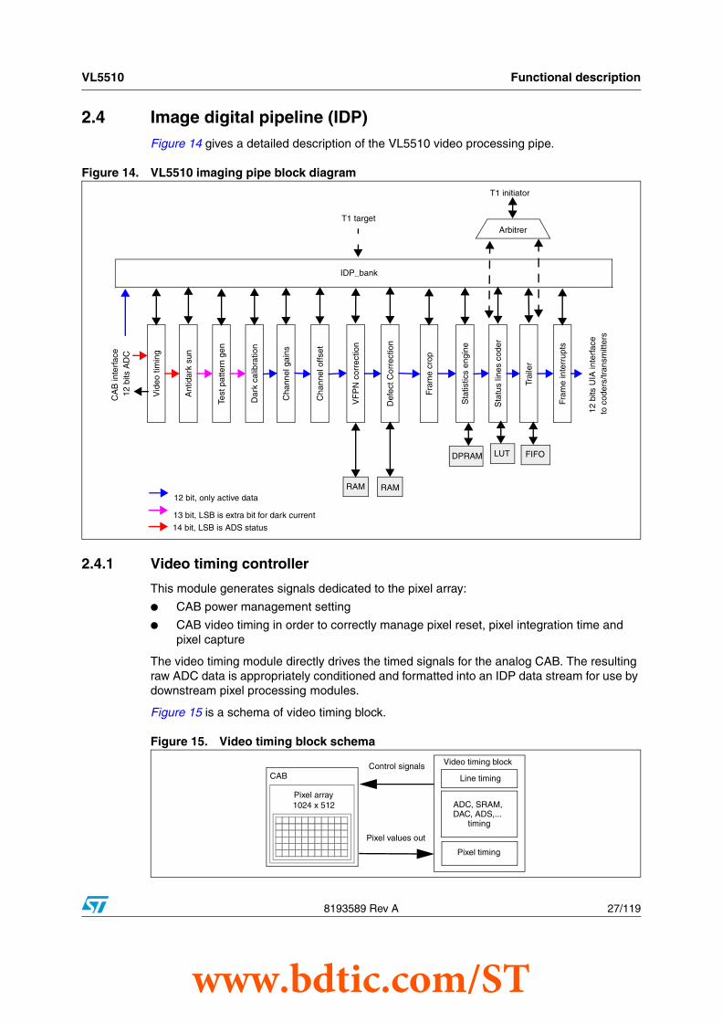
2.4 Image digital pipeline (IDP)Figure 14 gives a detailed description of the VL5510 video processing pipe.
Figure 14. VL5510 imaging pipe block diagram
2.4.1 Video timing controller
This module generates signals dedicated to the pixel array:
● CAB power management setting
● CAB video timing in order to correctly manage pixel reset, pixel integration time and pixel capture
The video timing module directly drives the timed signals for the analog CAB. The resulting raw ADC data is appropriately conditioned and formatted into an IDP data stream for use by downstream pixel processing modules.
Figure 15 is a schema of video timing block.
Figure 15. Video timing block schema
IDP_bank
T1 target
Vid
eo ti
min
g
12 bit, only active data
Test
pat
tern
gen
Dar
k ca
libra
tion
Cha
nnel
gai
ns
Cha
nnel
offs
et
VF
PN
cor
rect
ion
Def
ect C
orre
ctio
n
Fram
e cr
op
Sta
tistic
s en
gine
Sta
tus
lines
cod
er
Trai
ler
CA
B in
terf
ace
12 b
its A
DC
12 b
its U
IA in
terf
ace
to c
oder
s/tr
ansm
itter
s
Arbitrer
T1 initiator
RAM
LUTDPRAM FIFO
Ant
idar
k su
n
RAM
Fram
e in
terr
upts
14 bit, LSB is ADS status
13 bit, LSB is extra bit for dark current
Video timing block
ADC, SRAM,
Pixel timing
Line timing
DAC, ADS,... timing
Pixel array1024 x 512
CAB
Pixel values out
Control signals
www.bdtic.com/ST

Functional description VL5510
28/119 8193589 Rev A
Video timing mode
The video timing block allows the 3T pixel to be used with or without the high dynamic function.
In logarithmic mode, compression is applied to the active pixels by setting one or more knee points. A set of (soft) resets pulses with different strength are applied to perform the dynamic range (the strength is decreasing with the time for a given pixel/row).
2.4.2 Antidark sun correction
This module enables correction of the pixels that have been treated in the CAB by the antidark sun module. Correction is achieved through compensation of the offset generated by the ADS coupling (reset of a pixel that receives a very high level of light).
2.4.3 Test pattern generation
This module enables generation of a fixed video pattern that can be used for production tests or for debug purposes.
The test pattern generator inserts the test patterns defined in the SMIA v1.0 functional specification into an existing IDP. There are three full-frame test patterns defined:
● Solid color
● 100% color bars
● fade-to-50% grey color bars
There is also a separate horizontal and vertical cursor control which inserts the solid data value between the dynamically variable x and y limits within the output frame. These options are illustrated in Figure 16.
Figure 16. Fixed video pattern
Access to the block_IP is secured through the test pattern registers [0x0600 to 0x06FF] (see Section 6.3.9 on page 71) for which there is a specific protocol. A test image can only be generated if the user requests it.
Solid color 100% color bars Fade-to-50%color bars Cursors
www.bdtic.com/ST

VL5510 Functional description
8193589 Rev A 29/119
The following protocol should be followed to access the test pattern block registers.
● Write access to the test_pattern_protection [0x3380] register (see Section 6.3.10: Manufacturer specific registers [0x3000 to 0x34FF] on page 72). Data written should be 0xAE.
● Write access to the control registers test_pattern_mode_Hi [0x0600] and test_pattern_mode_Lo [0x0601] (see Section 6.3.9: Test pattern registers [0x0600 to 0x06FF] on page 71).
● If test_pattern_protection [0x3380] (see Section 6.3.10: Manufacturer specific registers [0x3000 to 0x34FF] on page 72) does not contain 0xAE data, the mode registers are reset (test mode cancelled).
2.4.4 Dark offset cancellation
In order to produce a high quality output image from the VL5510, it is necessary to accurately control the dark level of the video signal. Offset sources include:
● ramp generator under range setup
● offset created by dark current
VL5510 performs an automatic dark calibration, resulting in a black output level that remains constant over temperature and other variable conditions.
Dark lines
At the bottom of the pixel array there is a group of 16 rows which have the same exposure setting as the visible lines but are shielded from incident light. These are used to monitor the total offset in order that it can be removed from the image data.
Algorithm
For 12-bit data, the ideal ‘black’ code is set to a programmable value (when viewing 8-bit data the ‘black’ code should be 16). The aim of the dark calibration algorithm is to ‘learn’ the offset required so that ‘dark’ image lines have the programmed value. See Figure 17.
Figure 17. Role of dark offset calibration
1. The black line data which is used for FPN learning does not have the dark offset subtracted from it.
Raw image Processed image
Black line(1)
Ex. value = 200
Dark line
Ex. value = 400
Image line
Ex. value: 400 to 1360
Dark cal
Dark offset = 336
Black line(1)
Ex. value = 200
Dark line
Ex. value = 64
Image line
Ex. value: 64 to1024
www.bdtic.com/ST

Functional description VL5510
30/119 8193589 Rev A
Description
The dark line monitoring logic accumulates a number of dark pixels. It then calculates an average and compares this average with the appropriate black level.
The specific register, drk_mode_req [0x3003 bit 2:1] (see Section 6.3.10: Manufacturer specific registers [0x3000 to 0x34FF] on page 72), determines whether the offset applied is the user-programmable value from the serial register, or the value calculated by the offset cancellation processor.
The dark offset cancellation algorithm accumulates data from the dark lines which are input to a leaky integrator and an appropriate offset is calculated. When powering up or going out of suspend mode, or following an exposure/gain change, the history in the leaky integrator is reset to the incoming value as the previously stored value is out of date.
User control
The serial interface allows the user additional controls.
● Accumulation of dark pixels, calculation of dark pixel average and generation of a report. No application of any type is allowed to the data stream.
● Accumulation of dark pixels, calculation of dark pixel average, generation of a report and application of internally calculated offset to data stream.
● Accumulation of dark pixels, calculation of dark pixel average, generation of a report. Application of serial interface supplies offset.
Note: Internal clipping is enabled when using the user supplied offset. If too large a positive offset is supplied, the image clips to white. If too large a negative offset is supplied, the image clips to black.
2.4.5 Channel gain
Color dependent gains are applied to active pixel data within this module as part of the automatic white balance function.
The gain inputs are resynchronized to the first active line and are represented in an unsigned fixed point format with 8 bits right of the point that is, 0.0 <= comp < 16.
2.4.6 Channel offset
To achieve the desired black level of Bayer pixel data it is often necessary to apply an offset to the data. This module provides the functionality to apply a color channel-dependent offset on active pixel data, that is, not dark or black data.
2.4.7 Vertical fixed pattern noise (VFPN) correction
The goal of the VFPN cancellation module is to remove vertical fixed pattern noise. The VFPN is defined as the standard deviation over all columns of the average pixel voltage for each column determined at zero exposure and zero illumination. VFPN is expressed in mV.
Cancellation of this noise is achieved by use of a line RAM to ‘learn’ the average pixel values during the black lines of the frame. The difference between the black pixel average of each individual column (VFPN column average), and the black pixel average of the frame (VFPN signature), provides an offset. This offset is then added to (or subtracted from) the visible pixels during the active lines of the frame, resulting in cancellation of the noise.
www.bdtic.com/ST

VL5510 Functional description
8193589 Rev A 31/119
2.4.8 Defect correction
This module enables pixel correction on the image (defect pixel removal). The defect correction IP can be used for monochrome video streaming and for color video streaming.
The Scythe filter algorithm is implemented.
The input to scythe is a 5 x 5 pixel matrix from which a central pixel and a neighborhood of 8 pixels are extracted. The 8-pixel neighborhood is used to determine the validity of the corresponding central pixel. This is achieved using the ranked output of a Batcher-Banyan sort architecture. The scythe filter performs both detection and weighted correction on all data.
2.4.9 Crop
This module enables the cropping feature on the pixel array image. It can be used to decrease the system image size.
Cropping can be performed at different levels of the digital pipe:
● video timing
● crop IP
● output coder (when parallel mode is enabled)
The manufacturer specific registers [0x3000 - 0x34FF] (see Section 6.3.10 on page 72) enable the setting of the expected output image size. The input image is cropped based on these register settings.
To perform VTiming crop:
1. Disable crop module: set cr_enable [register 0x3330 - bit 0]: 0 disable.
2. Disable border extract module [register 0x335A = 0x00].
3. Change VTiming registers to the required values for cropping:
– VT X Start: [register 0x0344, register 0x0345]
– VT X End: [register 0x0348, register 0x0349]
– VT Y Start: [register 0x0346, register 0x0347]
– VT Y End: [register 0x034A, register 0x034B]
– VT X Output Size: [register 0x034C, register 0x034D]
– VT Y Output Size: [register 0x034E, register 0x034F]
4. If using a parallel interface, enable automatic mode for the output coder: register 0x3363 = 0x65.
www.bdtic.com/ST

Functional description VL5510
32/119 8193589 Rev A
To enable crop IP:
1. Enable Crop module: set cr_enable [register 0x3330 - bit 0]: 1 enable.
2. Set cr_mode [register 0x3330 - bit2:1]:
– 0X: Normal crop (status and dark lines are not delivered)
– 10: Only active lines are cropped, status and dark lines (status, dark and active)
– 11: Cropping is performed at all frame lines (status, dark and active)
3. Set the following registers at the required values:
– X Start [register 0x3332 and register 0x3333]
– Y Start [register 0x3334 and register 0x3335]
– X Size [register 0x3336 and register 0x3337]
– Y Size [register 0x3338 and register 0x3339]
– iActive Pixels: (register 0x333A, register 0x333B) should be equal to [(x_addr_end -x_addr_start +1) -(border_extract_left + border_ectract_right)] = [({0x0348, 0x0349} - {0x0345,0x0344} +1) -(0x335B +0x335C)]
– iActive lines: @(0x333C,0x333D) should be equal to (y_addr_end - y_addr_start +1) = ({0x034A,0x034B} - {0x0346,0x0347} +1)
4. If using a parallel interface (P12), disable automatic mode for the output coder:
– disable automatic mode for OPC: bit 0 of register 0x3363 = 0x00
– OPC H Start: (register 0x3364, register 0x3365) = crop x start + 3
– OPC H Stop: (register 0x3366, register 0x3367) = crop (xsize – x start + 1) + 3
– OPC Coarse Start: (register 0x3368, register 0x3369) = crop y start
– OPC Coarse Stop: (register 0x336A, register 0x336B) = crop (ysize – y start + 1)
– OPC Fine Start: (register 0x336C, register 0x336D) = crop x start
– OPC Fine Stop: (register 0x336E, register 0x336F) = crop (xsize – x start + 1)
To perform OPC crop (output coder crop) only using parallel interface (P12):
1. Disable crop module: set cr_enable [register 0x3330 - bit 0]: 0 disable.
2. Disable automatic mode for OPC: bit 0 of register 0x3363 = 0x00.
3. Set OPC register at required values for cropping:
– OPC H Start: (register 0x3364, register 0x3365) = H start value + 3
– OPC H Stop: (register 0x3366, register 0x3367) =H stop value + 3
– OPC Coarse Start: (register 0x3368, register 0x3369) = V start value
– OPC Coarse Stop: (register 0x336A, register 0x336B) = V stop value
– OPC Fine Start: (register 0x336C, register 0x336D) = H start value
– OPC Fine Stop: (register 0x336E, register 0x336F) = H stop value
www.bdtic.com/ST

VL5510 Functional description
8193589 Rev A 33/119
2.4.10 Statistic engine
The statistic engine module is used for histogram calculation to evaluate the image luminosity. Histogram describes gray value distribution of the frame and the data are directly delivered within lines embedded in the frame immediately after the last active line data.
Assuming a 12 bits pixel data, only the 8 bits MSB are used for histogram calculation. The histogram number n (0 to 255) describes how many pixel have a grey value in the range from n*16 to (n+1)*16 - 1. The histogram values are 24-bit values (20 bits are used, the remaining 4 bits are not used but no clipping is done) and they are used to describe the number of repeated grey code value in the active part of the frame.
Figure 18 is an overview of the statistic engine module.
Figure 18. Statistic engine module diagram overview
Histogram window
The histogram calculation is based on one determinate window specified by X and Y start/end input addresses. These addresses are relative to the current input active image. When the X or Y histogram start addresses are out of range of the input active image, the two flags hist_x_start_overflow and hist_y_start_overflow are then raised. When the X or Y histogram end addresses exceed the input active image size, then the two flags hist_x_end_overflow and hist_y_end_overflow become high.
To keep these flags low, the user should make sure that histogram window is inside the active input image otherwise the module would not be properly functional.
The histogram calculation is performed on one image window that is totally inside the active part of the image, this involves that no dark or black or status lines are processed in the calculations as shown in Figure 19.
0
20
40
60
80
100
value
1
value
2
value
3
value
256
value 1
value 2
value 3
value 256
Current frame
Statistic
lines
Active
12 bits data (8bit MSB only used)2^24(bits) = 2^20(max pixel array possible value) x 2^4(spare value)
The Trailer data is a sequence of 12 bits data words, the 12 bitdata words are transmitted in lines. Only 8bit are used , the upper 4 bits are unused
www.bdtic.com/ST

Functional description VL5510
34/119 8193589 Rev A
Figure 19. Histogram window
2.4.11 Status line coder
This module collects information (mainly system setting) inside the device and inserts the data inside an SMIA compatible video stream.
This module collects the content of specific registers (a list of which is stored in LUT ROM) and insert the data in the video frame.
The status line coder is used only in CCP mode. In other modes, the IP is bypassed. The status line coder supports 12 bits of data width.
2.4.12 Trailer
This module collects information inside the device and adds it to the end of the video stream. The output image contains the active video plus all status register information. Status registers are a subset of the VL5510 register map (see Table 13: Register map on page 50).
This module collects the content of the device registers status (+ histogram data).
Figure 20. Trailer diagram
LUT ROM contains addresses of registers which values will be sent on status data. These values registers are stored before in a dedicated RAM.
SOFDarkBlack
TRAILEREOF
Histogramwindow
x end
y end
x start
y_start
OutputTRAILERStart engine
LUT ROM
Bank
RAM
www.bdtic.com/ST

VL5510 Functional description
8193589 Rev A 35/119
2.4.13 Parallel 12-bit video interface
This module formats video output data and generates output video frame data on 12 bits together with synchronization signals (clock, vertical synchronization and horizontal synchronization).
The interface is fully programmable. The rising and falling edge position of the horizontal and vertical synchronization signals are programmable.
2.4.14 CCP Tx coder
This interface enables capture of video data using a CCP/SMIA standard LVDS interface.
This block is composed of:
● an smia_coder that packages the data specified in the SMIA (by inserting a CCP marker at beginning/end of each line)
● a CCP transmitter that serializes the data on the high speed interface
The VL5510 CCP output interface is compatible with CCP2 Class 0 transmitter (with extension to 250 Mbits/s - data/clock signaling), and with CCP2 Class 1 transmitter (with restriction to max data rate of 250 Mbits/s - data/strobe signaling), in conformity with SMIA Part 2: CCP2 specification - Revision 1.0 - 30-06-2004.
Data signaling
● Data/clock mode: data transfer is simple data signal and a continuous clock signal.
● Data/strobe mode: data transfer does not require a continuous clock signal. The data/strobe mode allows data to be sent over the two differential pairs with the clock embedded using specific logic in the transmitter side. The receiver logic reconstructs the clock and samples the data on both rising and falling clock edges. The data/strobe mode can transfer twice the amount of data at a given clock speed.
Data format
The CCP Tx coder supports 8-bit Raw Bayer data (RAW8), the 10-bit Raw Bayer data (RAW10) formats and the 12-bit Raw Bayer data (RAW12) formats.
RAW8
The 8-bit Raw Bayer data transmission is performed by transmitting the pixel data over CCP2 bus. However, the number of pixels between synchronization codes has to be a multiple of 4 pixels or a multiple of 4 bytes. Each line is separated by line start/end synchronization codes. This sequence is illustrated in Figure 21 (VGA case).
Bit order in transmission follows the general CCP2 rule, LSB first.
For 8-bit Raw Bayer, the suggested way of solving the false synchronization issue is to constrain the numerical range of pixel values from 1 to 255 (inclusive).
Figure 21. RAW8 data format in VGA case
www.bdtic.com/ST

Functional description VL5510
36/119 8193589 Rev A
Figure 22. RAW8 data transmission on CCP2 bus, bitwise illustration
Figure 23. RAW8 frame format in VGA case
RAW10
The transmission of 10-bit Raw Bayer data is accomplished by packing the 10-bit pixel data to look like 8-bit data format. The number of pixels between synchronization codes has to be a multiple of 16 pixels or a multiple of 20 bytes. Each line is separated by line start/end synchronization codes. This sequence is illustrated in Figure 24 (VGA case).
Bit order in transmission follows the general CCP2 rule, LSB first.
For 10-bit Raw Bayer, the suggested way to solve the false synchronization issue is to constrain the numerical range of pixel values from 4 to 1023 (inclusive). Also, every fifth byte (containing LSBs) has to be examined and force the bit 4 (P3 bit 0) to ‘1’ if the byte is all zeros.
www.bdtic.com/ST

VL5510 Functional description
8193589 Rev A 37/119
Figure 24. RAW10 data format in VGA case
Figure 25. RAW10 data transmission on CCP2 bus, bitwise illustration
Figure 26. RAW10 frame format in VGA case
RAW12
The transmission of 12-bit Raw Bayer data is also accomplished by packing the 12-bit pixel data to look like 8-bit data format. The number of pixels between synchronization codes has to be a multiple of 8 pixels or a multiple of 12 bytes. Each line is separated by line start/end synchronization codes. This sequence is illustrated in Figure 27 (VGA case).
Bit order in transmission follows the general CCP2 rule, LSB first.
For 12-bit Raw Bayer, the suggested way to solve the false synchronization issue is to constrain the numerical range of pixel values from 16 to 4095 (inclusive). Also, every third
byte (containing LSBs) has to be examined and force the bit 4 (P2 bit 0) to ‘1’ if the byte is all zeros.
Figure 27. RAW12 data format in VGA case
www.bdtic.com/ST

Functional description VL5510
38/119 8193589 Rev A
Figure 28. RAW12 transmission on CCP2 bus, bitwise illustration
Figure 29. RAW12 frame format in VGA case
www.bdtic.com/ST

VL5510 Functional description
8193589 Rev A 39/119
2.5 Imaging array - CAB frame formatFigure 30 gives the CAB frame format. It describes the physical content of the CAB array.
Figure 30. CAB frame format
Border pixels are used for defect correction.
Visible array
1024 pixels
1024 x 512 pixels
4 borders pixels
4 borders pixels
4 bo
rder
pix
els
4 bo
rder
pix
els
1040 pixels
512 pixels
520 pixels
524 pixels
2 dummy pixels
2 test pattern pixels
4 te
st p
atte
rn p
ixel
s
4 du
mm
y pi
xels
1032 pixels
www.bdtic.com/ST

Functional description VL5510
40/119 8193589 Rev A
2.6 Parallel interface frame formatVL5510 contains a parallel data output port (D[11:0]) plus associated qualification signals (HSYNC, VSYNC and PCLK).
Main features are:
● separate horizontal and vertical sync outputs
● fully programmable clock and sync - both position (sync only) and polarity
● tri-state output control allows multiple camera systems (port disabled upon reset)
● programmable frame/line blanking value
Figure 31 shows the frame format for the parallel interface.
Figure 31. Parallel interface output frame format
H b
lank
ing
V blankingH
bla
nkin
g
HSYNC
VS
YN
C
Active video
V blanking
dark lines
Trailer lines
VFPN lines
www.bdtic.com/ST

VL5510 Functional description
8193589 Rev A 41/119
2.7 CCP Tx frame formatFigure 32 indicates the frame formats for the CCP TX. These formats are defined in the SMIA normative (that is, the SMIA v1.0 functional specification).
Figure 32. CCP interface frame format
H b
lank
ing
First frame line - information line
Information line
Video line
Last frame line - statistic line
V blanking
H b
lank
ing
Statistic line
SOF EOL
EOL
EOLEOLEOFSOL
SOLSOL
SOL
SOL EOL
CC
P m
arke
r
CC
P m
arke
r
www.bdtic.com/ST

Functional description VL5510
42/119 8193589 Rev A
2.8 Sensor operating modesFigure 33 shows the VL5510 system state diagram.
Figure 33. VL5510 system state diagram
When the system is powered off, there is no activity.
When power is applied there are two possible stable states:
● low power state if XSHUTDOWN is maintained low
● standby state when XSHUTDOWN is high
At power-down, the device is reset to an internal power-on cell.
2.8.1 Low power state
The device is powered on but the XSHUTDOWN (regulator 1V2) is maintained low.
2.8.2 Standby state
When in standby state, the device is powered with the correct power supply (see Table 3: VL5510 signal description on page 10) and is capable of answering host commands. Access to all registers is possible, but no streaming is done.
2.8.3 Streaming state
When commanded, the sensor can start/stop streaming. In streaming mode, access to the registers is possible and the video is streamed out through the appropriate interface selected by mode pads.
2.8.4 Static parameter changes
Static parameter changes refers to anything that alters PLL setup, clock dividers and system configurations. It is an internal transient state. Access to it and exit from it is controlled by internal firmware. The sensor enters this state when the host asks for static parameter changes to be taken into consideration.
Low Power
Standby
Streaming
Power Up
Power down (OFF)
Power down (OFF)
Power down (ON)
Start Streaming Stop Streaming
Power down (ON)
Power down (ON)
Static Param
Automatic
Automatic
Automatic
Automatic
www.bdtic.com/ST

VL5510 Operation mode
8193589 Rev A 43/119
3 Operation mode
3.1 Mode definitionsThree mode pins are available on the chip. These pins are static. They set the mode after system power up. When the device is running no action on these pins is expected. To switch between two modes, the device should be switched off and on (action on power supply or on XSHUTDOWN pin).
Table 5 shows the mode definitions. An interface declared as ‘Off’ is not accessible.
The Osc column indicates whether the internal oscillator is set to enable use of an external quartz oscillator or whether the pad needs to be driven by an external clock source.
Table 5. VL5510 mode definitions
MODE[2:0] Osc I2CSPI
slaveUART
CCP + P12
SPI master
Comments
3’b000 Off On Off Off On On I2C + (CCP | P12) without oscillator
3’b001 On On Off Off On On I2C + (CCP | P12) with oscillator
3’b010 Off Off On Off On On SPI + (CCP | P12) without oscillator
3’b011 On Off On Off On On SPI + (CCP | P12) with oscillator
3’b100 Off Off Off On On On UART + (CCP | P12) without oscillator
3’b101 On Off Off On On On UART + (CCP | P12) with oscillator
3’b110 x x x x x x Reserved
3’b111 x x x x x x Reserved
www.bdtic.com/ST

High dynamic mode VL5510
44/119 8193589 Rev A
4 High dynamic mode
A good dynamic range is necessary to display a scene with the required details and contrast in a single image. Several methods exist to extend the dynamic range. The VL5510 high dynamic mode is based on a logarithmic response. To understand how this method works, it is necessary to explain first how a linear pixel is made.
4.1 Linear pixel responseThe pixel is a photoelectric cell of diode type mounted in inverse. The capacitor is charged until a known level and then discharged by the photocurrent generated by the photodiode during a time that is called the integration period. The saturation level corresponds to the discharge of the capacitor below the lowest readable pixel level.
Figure 34 below shows the linear pixel response curves depending on the amount of light received.
Figure 34. Linear pixel response curves
In Figure 34, Iphoto represents the photocurrent that is proportional to the illumination. The red curve shows the response of a pixel receiving high illumination and the green curve, the response of a pixel receiving low illumination. The relation between the output voltage, integration time and photocurrent is defined as:
where C is the capacitance and Tint is the integration time.
As seen in the formula, the slope of the pixel response curve versus the light intensity is proportional to the integration time. Figure 35 shows that the signal is proportional to the illumination until saturation.
Reset Voltage
Vsense_node
TimeTintegration0
dV/dt = -Iphoto5/C
dV/dt = -Iphoto4/C
dV/dt = -Iphoto3/C
dV/dt = -Iphoto2/C
dV/dt = -Iphoto1/C
= Saturation level
Vout(Iphoto5)=Vout(Iphoto4)=Vout(Iphoto3)
Vout(Iphoto2)
Vout(Iphoto1)
Reset Voltage
Vsense_node
TimeTintegration0
dV/dt = -Iphoto5/C
dV/dt = -Iphoto4/C
dV/dt = -Iphoto3/C
dV/dt = -Iphoto2/C
dV/dt = -Iphoto1/C
= Saturation level
Vout(Iphoto5)=Vout(Iphoto4)=Vout(Iphoto3)
Vout(Iphoto2)
Vout(Iphoto1)
Vout Iphoto Tint( ) C⁄×=Δ
www.bdtic.com/ST

VL5510 High dynamic mode
8193589 Rev A 45/119
Figure 35. Typical response
In order to avoid pixel saturation (as much as possible) and to increase the dynamic range, the VL5510 sensor can perform an integration by step for the high illuminated pixels.
4.2 High dynamic pixel responseThe objective for the high dynamic pixel response is to modify the way the pixel response is managed while keeping it linear. The voltage collected corresponds to the slope of the photocurrent curve (and no more to the voltage value). Figure 36 represents the pixel response with a dynamic range compression.
Figure 36. Pixel response with a dynamic range compression
With such a method, saturation is avoided even for very large photocurrents. A typical response is shown in Figure 37.
Illumination
(lux @ linear scale)
Vout
0 Illumination
(lux @ linear scale)
Vout
0
Vsense_node
Reset voltage = voltage control function
Tint
Vout(Iphoto1)dV/dt=-Iphoto1/C
Vout(Iphoto2)dV/dt=-Iphoto2/C
Vsense_node
Reset voltage = voltage control function
Tint
Vout(Iphoto1)dV/dt=-Iphoto1/C
Vout(Iphoto2)dV/dt=-Iphoto2/C
www.bdtic.com/ST

High dynamic mode VL5510
46/119 8193589 Rev A
Figure 37. High dynamic range typical response
The VL5510 sensor provides up to nine knee points. These knee points are used to reset the pixel during the overall integration period. The number of resets, their intensity and their positions are fully programmable.
Figure 38 shows an example of successive pixel resets to create the high dynamic mode.
Figure 38. High dynamic pixel response
The slope of the curves are the same as in Figure 34.
Vout
Illumination
(Lux@ linear scale)
Vout
Illumination
(Lux@ linear scale)
T3T2T1T0
V1
V2
V3
VDAC2 VDAC3
kp1 kp2 kp3V0 = Offset
V5 = VMax
= 4095 T4
VDAC1
VDAC4
kp4
V4
Read Date (sampling)
Reset Time
T3T2T1T0
V1
V2
V3
VDAC2 VDAC3
kp1 kp2 kp3V0 = Offset
V5 = VMax
= 4095 T4
VDAC1
VDAC4
kp4
V4
Read Date (sampling)
Reset Time
www.bdtic.com/ST

VL5510 Programming model
8193589 Rev A 47/119
5 Programming model
The VL5510 addressable register/memory space is configured as shown in Figure 39.
Figure 39. VL5510 addressable register/memory space
It consists of three principal areas each of which provide a different function.
● Code data. This area, which starts at address zero provides the interrupt vector table and the firmware code. Addresses A000 to A600 should be left empty for correct patch controlling.
● External data. This area is split into three sub-areas:
– Hardware registers: 0x0000 to 0x4000. This area provides direct access to the hardware registers associated with each functional block of the device. In normal operation, these registers are accessed under the control of the micro. They should never be accessed by the host system, however, they may be directly accessed by the host for debug and test purposes.
– Reserved: 0xA000 to 0xA600. This area is reserved.
– XDATA RAM: 0xE000 to 0xE800. This area provides temporary variable storage for the on-board micro.
● Internal data. This area contains the internal eWARP registers and the stack area. The remaining space is used for fast variables access.
www.bdtic.com/ST

Register description VL5510
48/119 8193589 Rev A
6 Register description
6.1 Register typeRegisters are split between user interface and hardware registers. A software abstraction layer provides mapping between the two. All user programming is achieved through the user interface registers although the hardware registers are also directly accessible for debug purposes.
6.2 User interface map
6.2.1 DeviceParameters [read only]
6.2.2 PrivateSetupUpdate
6.2.3 PrivateModeDin
Table 6. DeviceParameters
Index Byte Register name Data type Default Type Comment
0xE102 HiDevice_id 16UI 1FE RO The device ID is 510 (0x1FE)
0xE103 Lo
0xE104 FirmwareVsnMajor 8UI 1 RO The version major of firmware is 1
0xE105 FirmwareVsnMinor 8UI 0 RO The version minor of firmware is 0
0xE106 PatchVsnMajor 8UI 0 RO The version major of patch is 0
0xE107 PatchVsnMinor 8UI 0 RO The version minor of patch is 0
Table 7. PrivateSetupUpdate
Index Byte Register name Data type Default Type Comment
0x3AD1 SetupUpdate 8UI RW
The host write in this byte 1: setup update PLL and clocks
0: no setup update
1: setup update
Table 8. PrivateModeDin
Index Byte Register name Data type Default Type Comment
0x3A2A PrivateModeDin 8UI RW
Host choose output interface.
If host set bit 2: choose CCP interfaceIf host set bit 3: choose parallel interface
www.bdtic.com/ST

VL5510 Register description
8193589 Rev A 49/119
6.2.4 IcbSetupModeSelect
6.2.5 IcbSetupSoftwareReset
6.2.6 PrePllClkDiv
6.2.7 PllMultiplier
Table 9. IcbSetupModeSelect
Index Byte Register name Data type Default Type Comment
0x0100 SetupModeSelect 8UI RWThe host can write:0: stop stream
1: start stream
Table 10. IcbSetupSoftwareReset
Index Byte Register name Data type Default Type Comment
0x0103 SoftwareReset 8UI RW
The host can write:
0: no reset
1: reset
Table 11. PrePllClkDiv
Index Byte Register name Data type Default Type Comment
0x0304 HiPrePllClkDiv 16UI RW Pre PLL clock divider value
0x0305 Lo
Table 12. PllMultiplier
Index Byte Register name Data type Default Type Comment
0x0306 HiPllMultiplier 16UI RW PLL multiplier value
0x0307 Lo
www.bdtic.com/ST

Register description VL5510
50/119 8193589 Rev A
6.3 Register mapThe registers are grouped according to function with each group occupying a pre-allocated region of the address space.
The VL5510 registers are grouped into several different classes (see Table 13).
Any internal register that can be written to, can also be read from. There are also read only registers that contain device status information.
A read instruction from a reserved or unused register location returns the value 0x00.
A write instruction to a reserved or unused register location is illegal and the effect of such a write is undefined. It is the responsibility of the host system to only write to register locations which have been defined.
Table 13. Register map
Index Name of register group
Sensor registers: Configuration registers [0x0000 to 0x0FFF]
0x0000 to 0x00FF Status registers (dynamic, read only registers)
0x0100 to 0x01FF Setup registers – operating modes
0x0200 to 0x02FF Integration time and gain parameter registers
0x0300 to 0x03FF Video timing registers
0x0600 to 0x06FF Test pattern registers
Sensor registers: Parameter limit registers [0x1000 to 0x1FFF] (all registers are read only and static)
0x1000 to 0x10FF Integration time and gain parameter limits registers
0x1100 to 0x11FF Video timing parameter limits registers
Manufacturer specific registers [0x3000 to 0x34FF]
0x3000 to 0x34FF Manufacturer specific registers
Private registers [0x3800 to 0xFFF4]
0x3FFC to 0x4027 Reserved
0xA000 to 0xA600 Reserved
0xE000 to 0xE800 Xdata RAM
0xFFFx Test mode
www.bdtic.com/ST

VL5510 Register description
8193589 Rev A 51/119
6.3.1 Multi-byte register index space
This section defines the valid locations for MS and LS bytes of 16-bit and 32-bit register values.
For 16-bit wide registers the index of the MS byte must be a multiple of 2, that is, the LS bit of the 16-bit index must be zero.
For 32-bit wide registers the index of the MS byte must be a multiple of 4 that is, the two LS bits of the 16-bit index must be zero.
Table 14. Valid 16-bit indices for the MS data byte of 16-bit wide register
16-bit register 16-bit register
MS data byte LS data byte MS data byte LS data byte
65532 65533 65534 65535
65528 65529 65530 65531
65524 65525 65526 65527
65520 65521 65522 65523
| | | |
12 13 14 15
8 9 10 11
4 5 6 7
0 1 2 3
Table 15. Valid 16-bit indices for the MS and LS data bytes of 32-bit wide registers
32-bit register
MS data byte LS data byte
65532 65533 65534 65535
65528 65529 65530 65531
65524 65525 65526 65527
65520 65521 65522 65523
| | | |
12 13 14 15
8 9 10 11
4 5 6 7
0 1 2 3
www.bdtic.com/ST

Register description VL5510
52/119 8193589 Rev A
6.3.2 Data alignment within registers
If the width of an internal register is narrower than the 8-bit, 16-bit or 32-bit register which reports its value, then the register value is right aligned within the register and the unused MS bits are padded with zeroes.
Figure 40. Right alignment for packing 10-bit data into two 8-bit registers
6.3.3 Valid register data types
A number of different data types are represented in the various register contents. Table 16 explains the different types.
7 3 16 5 4 2 0
7 3 1 6 5 4 2 0 9 8
7 3 1 6 5 4 2 0
Hi Byte (MSB) Lo Byte (LSB)
Internal 10-bit Register Value
Top bits padded with
zeroes
Table 16. Valid register data types
Data type Name Range Description
8UI 8-bit unsigned integer 0 to 255
8SI 8-bit signed integer -128 to 127 Two’s complement notation.
16UI 16-bit unsigned integer 0 to 65535
16SI 16-bit signed integer -32768 to 32767 Two’s complement notation.
16UR 16-bit unsigned iReal 0 to 255.9960937508.08 fixed point number. 8 integer bits (MS byte), 8 fractional bits (LS byte).
16SR 16-bit signed iReal -128 to 127.9960375Two’s complement notation, 8 fractional bits.
32UR 32-bit unsigned iReal 0 to 65535.9999847416.16 fixed point number. 16 integer bits (MS 2 bytes), 16 fractional bits (LS 2 bytes).
32SR 32-bit signed iReal-32768 to 32767.99998474
Two’s complement notation,16 fractional bits.
32SF32-bit IEEE floating-point number
As per IEEE 754As per IEEE 754. 1 sign bit, 8 exponent bits, 23 fractional bits.
8C or 16C 8-bit or 16-bit coded -This indicates that the value is decoded to select one of several functions or modes.
8B or 16B 8 or 16 bits -Each bit represents a specific function or mode.
www.bdtic.com/ST

VL5510 Register description
8193589 Rev A 53/119
6.3.4 Status registers [0x0000 to 0x000F]
Table 17 lists the status registers which are read only and dynamic.
Table 17. Status registers [0x0000 to 0x000F](1)
Index Byte Register nameData type
Default Type Comment
0x0000 Himodel_id 16UI 01.FE RO
16-bit sensor model number that is, 51010.0x0001 Lo
0x0002 revision_number 8UI 00.00 ROChip version ID For VL5510 rev 0.0 silicon revision is 0x0000.
0x0003 manufacturer_id 8C 01 RO Manufacturer ID: ST micro.
0x0005 frame_count 8UI FF RO
Frame count increments by 1 on each frame. Rolls over at 255 to 0. When moving from video to sleep the frame count is reset to 255. The frame count is reset to 255 after a soft reset (register 0x0103).
0x0006 pixel_order_status 8C 00 RO
Color pixel readout orderDefines the order of the color pixel readout. Changes with mirror and flip (register 0x0101).0x00 - GR/BG - normal0x01 - RG/GB - horizontal mirror0x02 - BG/GR - vertical flip0x03 - GB/RG - vertical flip and horizontal mirror
0x0007 Reserved - - - -
1. Abbreviations: Hi = high, Lo = low, and RO = read only.
www.bdtic.com/ST

Register description VL5510
54/119 8193589 Rev A
6.3.5 Frame format description registers [0x0040 to 0x007F]
Figure 41 shows the frame format.
Figure 41. Frame format
Table 18 lists the frame format description registers.
H b
lank
ing
Start of frame line - LTYPE_SOF
Dark line - LTYPE_DARK_NOMDark line - LTYPE_DARK_LAST
Active line - LTYPE_ACTIVE_NOM
Active line - LTYPE_ACTIVE_LAST
End of frame - LTYPE_EOF
V blanking
H b
lank
ing
henv
Trailer line - LTYPE_STATUS
Black line - LTYPE_BLACK_NOM
Black line - LTYPE_BLACK_LAST
Table 18. Frame format description registers [0x0040 to 0x007F](1)
Index Byte Register nameData type
Default Type Comment
0x0040 frame_format_model_type 8C 01 R/W
Generic frame format. 0x01: 2-byte data format (see Section 2.4.3: Test pattern generation on page 28)
0x0041 frame_format_model_subtype 8C 26 R/W
Contains a number of 2-byte data format descriptors. Upper nibble defines the number of column descriptors, for example, 2Lower nibble defines the number of row descriptors, for example, 6.
0x0042 Hi
frame_format_descriptor_0 16C 54.10 R/W
Pixel data code: 5 (visible columns)Number of pixels: readout dependentMaximum number of pixels: 1040Number of pixels: 1040
0x0043 Lo
www.bdtic.com/ST

VL5510 Register description
8193589 Rev A 55/119
The format of the 2-byte descriptor is shown in Figure 42.
Figure 42. 2-byte generic field format descriptor
1. Legend:Pixel code (top 4 bits in the MS byte): Defines the type of pixel data, that is, embedded, dummy, black, dark, visible or manufacturer specific.Number of pixels: 12-bit (bottom 4 bits in the MS byte and the LS byte).
0x0044 Hiframe_format_descriptor_1 16C 20.08 R/W
Pixel data code: 2 (dummy columns)Number of pixels: 80x0045 Lo
0x0046 Hiframe_format_descriptor_2 16C 10.03 R/W
Pixel data code: 1 (embedded data lines)Number of lines: 30x0047 Lo
0x0048 Hiframe_format_descriptor_3 16C 30.04 R/W
Pixel data code: 8 (Black lines)Number of lines: 40x0049 Lo
0x004A Hiframe_format_descriptor_4 16C 40.10 R/W
Pixel data code: 4 (dark lines)Number of lines: 160x004B Lo
0x004C Hi
frame_format_descriptor_5 16C 52.08 R/W
Pixel data code: 5 (visible lines)Number of lines: readout dependentMaximum number of lines: 520
0x004D Lo
0x004E HI
frame_format_descriptor_6 16C 80.02 R/W
Pixel data code: 6(trailer lines)Number of lines: readout dependentMinimum number of lines: 2
0x004F LO
0x0050 HIframe_format_descriptor_7 16C 9001 R/W Pixel data code: 7 (end lines)
0x0051 LO
1. Abbreviations: Hi = high, Lo = low, and R/W = read/write.
Table 18. Frame format description registers [0x0040 to 0x007F](1) (continued)
Index Byte Register nameData type
Default Type Comment
B7 B0
Pixel code N[11:8] N[7:0]
B0B3B4 B7
High byte Low byte
4-bit pixel data code Number of pixels, 12-bit, N[11:0]
N [11:8] N [7:0]
(0 to 4095 bytes)
www.bdtic.com/ST

Register description VL5510
56/119 8193589 Rev A
Table 19 provides an explanation of the pixel data code.
6.3.6 Setup registers [0x0100 to 0x01FF]
Table 20 lists the setup registers.
Table 19. Pixel data code
Code Pixel data Code Pixel data
0 Illegal 8 Manufacturer specific pixel type 0
1 Embedded data 9 Manufacturer specific pixel type 1
2 Dummy pixel data 10 Manufacturer specific pixel type 2
3 Black pixel data 11 Manufacturer specific pixel type 3
4 Dark pixel data 12 Manufacturer specific pixel type 4
5 Visible pixel data 13 Manufacturer specific pixel type 5
6 Reserved 14 Manufacturer specific pixel type 6
7 Reserved 15 Illegal
Table 20. Setup registers [0x0100 to 0x01FF](1)
Index Byte Register nameData type
Default Type Comment
0x0100 - mode_select 8UI 00 R/W
Mode select0x00 - software standby0x01 - streamingFor a full description, refer to the SMIA v1.0 functional specification, Section 3: Operating modes.
0x0101 - image_orientation 8B 00 R/W
Image orientation, that is, horizontal mirror and vertical flip.Bit 0: 0 - no mirror, 1 - horizontal mirror enableBit 1: 0 - no flip, 1 - vertical flip enable
0x0102 - Reserved - - - -
0x0103 - software_reset 8UI 00 R/W
Software reset. Setting this register to 1 resets the sensor to its power up defaults. The value of this bit is also reset.0x00 - normal0x01 - soft resetFor a full description, refer to the SMIA v1.0 functional specification, Section 3: Operating modes.
www.bdtic.com/ST

VL5510 Register description
8193589 Rev A 57/119
0x0104 - grouped_parameter_hold 8UI 00 R/W
The grouped parameter hold register disables the consumption of integration, gain and video timing parameters.0x00 - consumes parameters as normal0x01 - holds parametersFor a full description, refer to the SMIA v1.0 functional specification, Section 6.5: Re-timing of integration time and gain control.
0x0105 - mask_corrupted_frames 8UI 00 R/W
Setting this register to 1 prevents the sensor outputting frames that have been corrupted by video timing parameter changes.0x00 - normal0x01 - mask corrupted frames
0x0110 - csi_channel_ident[3:0] 8UI 00 R/W
bit3:0: The csi_channel_identifier register allows the DMA channel identifier within the CSI embedded synchronization codes to be programmed. The default value for this register is 0x00 for backward compatibility with older CSI receivers.Valid range: 0-7
0x0111 - csi_signalling_mode 8UI 01 R/W
bit0: 0 - Data/clock signalling: positive edge of the data qualification clock qualifies the data.1 - Data/strobe signalling
Table 20. Setup registers [0x0100 to 0x01FF](1) (continued)
Index Byte Register nameData type
Default Type Comment
www.bdtic.com/ST

Register description VL5510
58/119 8193589 Rev A
6.3.7 Integration time and gain registers [0x0200 to 0x02FF]
Table 21 lists the integration time and gain registers which are used to control the image exposure.
0x0112 Hi csi_data_format_hi[3:0]
16UI 0A0A RW
bit3:0:The MS byte of the csi_data_format register contains the bit width of the uncompressed pixel data.bit3:0:The LS byte of the csi_data_format register contains the bit width of the compressed pixel data.See Table 18 on page 54 for valid values.
0x0113 Lo csi_data_format_lo[3:0]
0x0114 - coder_x_dummy_size[4:0] 8U 00 RW
bit4:0:16 - this register value = Number of dummy pixels added per line. Valid range is 0 to 16.ccp10: Total pixels per line (between synchronization codes) must be a multiplier of 16 or 20 bytes.ccp8: Total pixels per line (between synchronization codes) must be a multiplier of 32 bytes.ccp12: Total pixels per line (between synchronization codes) must be a multiplier of 12 bytes.
1. Abbreviations: Hi = high, Lo = low, R/W = read/write, and RO = read only.
Table 20. Setup registers [0x0100 to 0x01FF](1) (continued)
Index Byte Register nameData type
Default Type Comment
Table 21. Integration time and gain registers [0x0200 - 0x02FF](1)
Index Byte Register nameData type
Default Type Comment
0x0200 Hibit3:0: fine_integration_time[11:8]
16UI 00.07 R/W
Fine integration time (pixels). The default value cannot be below 7 decimal for analog readout corruption reasons. 0x0201 Lo bit7:0: fine_integration_time[7:0]
0x0202 Hi bit5:0: coarse_integration_time16UI 00.14 R/W
Coarse integration time (lines). The upper limit depends on the vertical line blanking value.0x0203 Lo bit7:0: coarse_integration_time
0x0204 Hi bit7:0: 00
16UI 00.00 R/WSee description below and refer to Table 22: Analog gain ranges.0x0205 Lo
bit7:4: analog_gain_code_global
1. Abbreviations: Hi = high, Lo = low, and R/W = read/write.
www.bdtic.com/ST

VL5510 Register description
8193589 Rev A 59/119
VL5510 has a single global analog gain which means the analog gain applied for red, greenR, greenB or blue pixels is the same. The registers 0x0080 and 0x0081 (analog_gain_capability) are set to 0 for this reason.
VL5510 has a 16-bit register to control analog gain. However, only 4 bits are supported. Figure 43 shows how the analog gain bits are used by VL5510.
Figure 43. Analog gain bits
Table 22. Analog gain ranges
Gain code Binary gain code Coarse analog gain
0 0000 0 dB
1 0001 0.56 dB
2 0010 1.16 dB
3 0011 1.8 dB
4 0100 2.5 dB
5 0101 3.25 dB
6 0110 4.1 dB
7 0111 5.0 dB
8 1000 6.0 dB
9 1001 7.2 dB
10 1010 8.5 dB
11 1011 10.1 dB
12 1100 12 dB
13 1101 14.5 dB
14 1110 18.1 dB
15 1111 24.1 dB
A7 A5 A4A6A8A9A15 A14 A13 A12 A11 A10
Binary gain code Not usedNot used
A0A1A3 A2
www.bdtic.com/ST

Register description VL5510
60/119 8193589 Rev A
6.3.8 Video timing registers [0x0300 to 0x03FF]
The video stream which is output from the VL5510 contains both video data and other auxiliary information.
Table 23 lists the video timing registers.
Table 23. Video timing registers [0x0300 to 0x03FF](1)
Index Byte Register nameData type
Default Type Comment
0x0300 Hibit0:3: vt_pix_clk_div 16UI 00.0A RW
Video timing pixel clock dividerValue: 100x0301 Lo
0x0302 Hibit0:3: vt_sys_clk_div 16UI 00.02 RW
Video timing system clock divider value.Value: 20x0303 Lo
0x0304 Hibit0:3: pre_pll_div 16UI 00.04 RW
Pre PLL clock divider valueValue:80x0305 Lo
0x0306 Hibit0:7: pll_mult 16UI 00.38 RW
PLL multiplier valueValue: 560x0307 Lo
0x0340 Hi bit7:0: frame_length_lines[13:8]16UI 02.23 RW
Frame lengthUnits: LinesValue: 5470x0341 Lo bit7:0: frame_length_lines[7:0]
0x0342 Hi bit3:0: line_lenght_pck[11:8]16UI 05.3E RW
Line lengthUnits: Pixel ClocksValue: 13420x0343 Lo bit7:0: line_lenght_pck[7:0]
0x0344 Hi bit2:0: x_addr_start[10:8]
16UI 00.00 RW
X-address of the top left corner of the visible pixel dataUnits: PixelsValue: 0
0x0345 Lo bit7:0: x_addr_start[7:0]
0x0346 Hi bit1:0: y_addr_start[9:8]
16UI 00.00 RW
Y-address of the top left corner of the visible pixel dataUnits: LinesValue: 0
0x0347 Lo bit7:0: y_addr_start[7:0]
0x0348 Hi bit2:0: x_addr_end[10:8]
16UI 04.0F RW
X-address of the bottom right corner of the visible pixel dataUnits: PixelsValue: 1039
0x0349 Lo bit7:0: x_addr_end[7:0]
0x034A Hi bit1:0: y_addr_end[9:8]
16UI 02.07 RW
Y-address of the bottom right corner of the visible pixel dataUnits: LinesValue:519
0x034B Lo bit7:0: y_addr_end[7:0]
0x034C Hi bit2:0: x_output_size[10:8]
16UI 04.00 RW
Width of image data output from the sensor (used only by OPC module)Units: PixelsValue: 1024
0x034D Lo bit7:0: x_output_size[7:0]
www.bdtic.com/ST

VL5510 Register description
8193589 Rev A 61/119
0x034E Hi bit1:0: y_output_size[9:8]
16UI 02.00 RW
Height of image data output from the sensor (used only by OPC module)Units: LinesValue: 512
0x034F Lo bit7:0: y_output_size[7:0]
0x0380 Hi bit7:0: 0016UI 00.01 RW
Increment for even pixels in the readout orderValue: 10x0381 Lo bit2:0: x_even_inc[2:0]
0x0382 Hi bit7:0: 0016UI 00.01 RW
Increment for odd pixels in the readout orderValue: 10x0383 Lo bit2:0: x_odd_inc[2:0]
0x0384 Hi bit7:0: 0016UI 00.01 RW
Increment for odd pixels in the readout ordervalue:10x0385 Lo bit2:0: y_even_inc[2:0]
0x0386 Hi bit7:0: 0016UI 00.01 RW
Increment for odd pixels in the readout ordervalue: 10x0387 Lo bit2:0: y_odd_inc[2:0]
0x0388 -bit7:0: even_frame_dac_val_0[7:0]
8UI 14 RW
Dac value which corresponds to the first knee point.Default value: 20Application: EVEN Frames
0x0389 -bit7:0: even_frame_dac_val_1[7:0]
8UI 28 RW
Dac value which corresponds to the knee point N 2.Default value: 40Application: EVEN Frames
0x038A -bit7:0: even_frame_dac_val_2[7:0]
8UI 3C RW
Dac value which corresponds to the knee point N 3.Default value: 60 Application: EVEN Frames
0x038B -bit7:0: even_frame_dac_val_3[7:0]
8UI 50 RW
Dac value which corresponds to the knee point N 4.Default value: 80Application: EVEN Frames
0x038C -bit7:0: even_frame_dac_val_4[7:0]
8UI 64 RW
Dac value which corresponds to the knee point N 5.Default value: 100Application: EVEN Frames
0x038D -bit7:0: even_frame_dac_val_5[7:0]
8UI 78 RW
Dac value which corresponds to the knee point N 6.Default value: 120Application: EVEN Frames
Table 23. Video timing registers [0x0300 to 0x03FF](1) (continued)
Index Byte Register nameData type
Default Type Comment
www.bdtic.com/ST

Register description VL5510
62/119 8193589 Rev A
0x038E -bit7:0: even_frame_dac_val_6[7:0]
8UI 8C RW
Dac value which corresponds to the knee point N 7.Default value: 140Application: EVEN Frames
0x038F -bit7:0: even_frame_dac_val_7[7:0]
8UI A0 RW
Dac value which corresponds to the knee point N 8.Default value: 160Application: EVEN Frames
0x0390 -bit7:0: even_frame_dac_val_8[7:0]
8UI B4 RW
Dac value which corresponds to the knee point N 9.Default value: 180Application: EVEN Frames
0x0391 -bit7:0: even_frame_dac_val_9[7:0]
8UI C8 RW
Dac value which corresponds to the knee point N 10.Default value: 200Application: EVEN Frames
0x0392 -bit7:0: odd_frame_dac_val_0[7:0]
8UI 14 RW
Dac value which corresponds to the first knee point.Default value: 20Application: ODD Frames
0x0393 -bit7:0: odd_frame_dac_val_1[7:0]
8UI 28 RW
Dac value which corresponds to the knee point N 2.Default value: 40Application: ODD Frames
0x0394 -bit7:0: odd_frame_dac_val_2[7:0]
8UI 3C RW
Dac value which corresponds to the knee point N 3.Default value: 60Application: ODD Frames
0x0395 -bit7:0: odd_frame_dac_val_3[7:0]
8UI 50 RW
Dac value which corresponds to the knee point N 4.Default value: 80Application: ODD Frames
0x0396 -bit7:0: odd_frame_dac_val_4[7:0]
8UI 64 RW
Dac value which corresponds to the knee point N 5.Default value: 100Application: ODD Frames
0x0397 -bit7:0: odd_frame_dac_val_5[7:0]
8UI 78 RW
Dac value which corresponds to the knee point N 6.Default value: 120Application: ODD Frames
Table 23. Video timing registers [0x0300 to 0x03FF](1) (continued)
Index Byte Register nameData type
Default Type Comment
www.bdtic.com/ST
VL5510 Register description
8193589 Rev A 63/119
0x0398 -bit7:0: odd_frame_dac_val_6[7:0]
8UI 8C RW
Dac value which corresponds to the knee point N 7.Default value: 140Application: ODD Frames
0x0399 -bit7:0: odd_frame_dac_val_7[7:0]
8UI A0 RW
Dac value which corresponds to the knee point N 8.Default value: 160Application: ODD Frames
0x039A -bit7:0: odd_frame_dac_val_8[7:0]
8UI B4 RW
Dac value which corresponds to the knee point N 9.Default value: 180Application: ODD Frames
0x039B -bit7:0: odd_frame_dac_val_9[7:0]
8UI C8 RW
Dac value which corresponds to the knee point N 10.Default value: 200Application: ODD Frames
0x039E Hibit7:0: even_frame_y_offset_0[15:8]
16UI 00.12 RW
Address of the first knee point (number of lines between the line to reset and the current read line (end of integration)).If y_offsetx=0 => it is a fine knee point.Default value: 18Application: EVEN Frames
0x039F Lobit7:0: even_frame_y_offset_0[7:0]
0x03A0 Hibit7:0: even_frame_y_offset_1[15:8]
16UI 00.10 RWAddress of the knee point N 2Default value: 16Application: EVEN Frames0x03A1 Lo
bit7:0: even_frame_y_offset_1[7:0]
0x03A2 Hibit7:0: even_frame_y_offset_2[15:8]
16UI 00.0F RWAddress of the knee point N 3Default value: 15Application: EVEN Frames0x03A3 Lo
bit7:0: even_frame_y_offset_2[7:0]
0x03A4 Hibit7:0: even_frame_y_offset_3[15:8]
16UI 00.0D RWAddress of the knee point N 4Default value: 13Application: EVEN Frames0x03A5 Lo
bit7:0: even_frame_y_offset_3[7:0]
0x03A6 Hibit7:0: even_frame_y_offset_4[15:8]
16UI 00.09 RWAddress of the knee point N 5Default value: 9Application: EVEN Frames0x03A7 Lo
bit7:0: even_frame_y_offset_4[7:0]
Table 23. Video timing registers [0x0300 to 0x03FF](1) (continued)
Index Byte Register nameData type
Default Type Comment
www.bdtic.com/ST

Register description VL5510
64/119 8193589 Rev A
0x03A8 Hibit7:0: even_frame_y_offset_5[15:8]
16UI 00.07 RWAddress of the knee point N 6Default value: 7Application: EVEN Frames0x03A9 Lo
bit7:0: even_frame_y_offset_5[7:0]
0x03AA Hibit7:0: even_frame_y_offset_6[15:8]
16UI 00.05 RWAddress of the knee point N 7Default value: 5Application: EVEN Frames0x03AB Lo
bit7:0: even_frame_y_offset_6[7:0]
0x03AC Hibit7:0: even_frame_y_offset_7[15:8]
16UI 00.03 RWAddress of the knee point N 8Default value: 3Application: EVEN Frames0x03AD Lo
bit7:0: even_frame_y_offset_7[7:0]
0x03AE Hibit7:0: even_frame_y_offset_8[15:8]
16UI 00.00 RWAddress of the knee point N 9Default value: 0Application: EVEN Frames0x03AF Lo
bit7:0: even_frame_y_offset_8[7:0]
0x03B0 Hibit7:0: even_frame_y_offset_9[15:8]
16UI 00.00 RWAddress of the knee point N 10Default value: 0Application: EVEN Frames0x03B1 Lo
bit7:0: even_frame_y_offset_9[7:0]
0x03B2 Hibit7:0: odd_frame_y_offset_0[15:8]
16UI 00.12 RWAddress of the first knee point Default value: 18Application: ODD Frames0x03B3 Lo
bit7:0: odd_frame_y_offset_0[7:0]
0x03B4 Hibit7:0: odd_frame_y_offset_1[15:8]
16UI 00.10 RWAddress of the knee point N 2Default value: 16Application: ODD Frames0x03B5 Lo
bit7:0: odd_frame_y_offset_1[7:0]
0x03B6 Hibit7:0: odd_frame_y_offset_2[15:8]
16UI 00.0F RWAddress of the knee point N 3Default value: 15Application: ODD Frames0x03B7 Lo
bit7:0: odd_frame_y_offset_2[7:0]
0x03B8 Hibit7:0: odd_frame_y_offset_3[15:8]
16UI 00.0D RWAddress of the knee point N 4Default value: 13Application: ODD Frames0x03B9 Lo
bit7:0: odd_frame_y_offset_3[7:0]
0x03BA Hibit7:0: odd_frame_y_offset_4[15:8]
16UI 00.09 RWAddress of the knee point N 5Default value: 9Application: ODD Frames0x03BB Lo
bit7:0: odd_frame_y_offset_4[7:0]
Table 23. Video timing registers [0x0300 to 0x03FF](1) (continued)
Index Byte Register nameData type
Default Type Comment
www.bdtic.com/ST

VL5510 Register description
8193589 Rev A 65/119
0x03BC Hibit7:0: odd_frame_y_offset_5[15:8]
16UI 00.07 RWAddress of the knee point N 6Default value: 7Application: ODD Frames0x03BD Lo
bit7:0: odd_frame_y_offset_5[7:0]
0x03BE Hibit7:0: odd_frame_y_offset_6[15:8]
16UI 00.05 RWAddress of the knee point N 7Default value: 5Application: ODD Frames0x03BF Lo
bit7:0: odd_frame_y_offset_6[7:0]
0x03C0 Hibit7:0: odd_frame_y_offset_7[15:8]
16UI 00.03 RWAddress of the knee point N 8Default value: 3Application: ODD Frames0x03C1 Lo
bit7:0: odd_frame_y_offset_7[7:0]
0x03C2 Hibit7:0: odd_frame_y_offset_8[15:8]
16UI 00.00 RWAddress of the knee point N 9Default value: 0Application: ODD Frames0x03C3 Lo
bit7:0: odd_frame_y_offset_8[7:0]
0x03C4 Hibit7:0: odd_frame_y_offset_9[15:8]
16UI 00.00 RWAddress of the knee point N 10Default value: 0Application: ODD Frames0x03C5 Lo
bit7:0: odd_frame_y_offset_9[7:0]
0x03C6 Hibit7:0: even_frame_x_addr_0[15:8]
16UI 00.14 RW
The position where the first knee point rise on the current read line (line_length -x_addr0) pixels before sampling the current line.Unit: pixelsDefault value: 20Application: EVEN Frames
0x03C7 Lobit7:0: even_frame_x_addr_0[7:0]
0x03C8 Hibit7:0: even_frame_x_addr_1[15:8]
16UI 00.28 RW
The position where the knee point N 2 rise on the line timing.Unit: pixelsDefault value: 40Application: EVEN Frames
0x03C9 Lobit7:0: even_frame_x_addr_1[7:0]
0x03CA Hibit7:0: even_frame_x_addr_2[15:8]
16UI 00.32 RW
The position where the knee point N 3 rise on the line timing.Unit: pixelsDefault value: 50Application: EVEN Frames
0x03CB Lobit7:0: even_frame_x_addr_2[7:0]
0x03CC Hibit7:0: even_frame_x_addr_3[15:8]
16UI 00.46 RW
The position where the knee point N 4 rise on the line timing.Unit: pixelsDefault value: 70Application: EVEN Frames
0x03CD Lobit7:0: even_frame_x_addr_3[7:0]
Table 23. Video timing registers [0x0300 to 0x03FF](1) (continued)
Index Byte Register nameData type
Default Type Comment
www.bdtic.com/ST

Register description VL5510
66/119 8193589 Rev A
0x03CE Hibit7:0: even_frame_x_addr_4[15:8]
16UI 00.5A RW
The position where the knee point N 5 rise on the line timing.Unit: pixelsDefault value: 90Application: EVEN Frames
0x03CF Lobit7:0: even_frame_x_addr_4[7:0]
0x03D0 Hibit7:0: even_frame_x_addr_5[15:8]
16UI 00.6E RW
The position where the knee point N 6 rise on the line timing.Unit: pixelsDefault value: 110Application: EVEN Frames
0x03D1 Lobit7:0: even_frame_x_addr_5[7:0]
0x03D2 Hibit7:0: even_frame_x_addr_6[15:8]
16UI 00.82 RW
The position where the knee point N 7 rise on the line timing.Unit: pixelsDefault value: 130Application: EVEN Frames
0x03D3 Lobit7:0: even_frame_x_addr_6[7:0]
0x03D4 Hibit7:0: even_frame_x_addr_7[15:8]
16UI 00.96 RW
The position where the knee point N 8 rise on the line timing.Unit: pixelsDefault value: 150Application: EVEN Frames
0x03D5 Lobit7:0: even_frame_x_addr_7[7:0]
0x03D6 Hibit7:0: even_frame_x_addr_8[15:8]
16UI 00.AA RW
The position where the knee point N 9 rise on the line timing.Unit: pixelsDefault value: 170Application: EVEN Frames
0x03D7 Lobit7:0: even_frame_x_addr_8[7:0]
0x03D8 Hibit7:0: even_frame_x_addr_9[15:8]
16UI 00.BE RW
The position where the knee point N 10 rise on the line timing.Unit: pixelsDefault value: 190Application: EVEN Frames
0x03D9 Lobit7:0: even_frame_x_addr_9[7:0]
0x03DA Hibit7:0: odd_frame_x_addr_0[15:8]
16UI 00.14 RW
The position where the first knee point rise on the line timing.Unit: pixelsDefault value: 20Application: ODD Frames
0x03DB Lobit7:0: odd_frame_x_addr_0[7:0]
0x03DC Hibit7:0: odd_frame_x_addr_1[15:8]
16UI 00.28 RW
The position where the knee point N 2 rise on the line timing.Unit: pixelsDefault value: 40Application: ODD Frames
0x03DD Lobit7:0: odd_frame_x_addr_1[7:0]
Table 23. Video timing registers [0x0300 to 0x03FF](1) (continued)
Index Byte Register nameData type
Default Type Comment
www.bdtic.com/ST

VL5510 Register description
8193589 Rev A 67/119
0x03DE Hibit7:0: odd_frame_x_addr_2[15:8]
16UI 00.32 RW
The position where the knee point N 3 rise on the line timing.Unit: pixelsDefault value: 50Application: ODD Frames
0x03DF Lobit7:0: odd_frame_x_addr_2[7:0]
0x03E0 Hibit7:0: odd_frame_x_addr_3[15:8]
16UI 00.46 RW
The position where the knee point N 4 rise on the line timing.Unit: pixelsDefault value: 70Application: ODD Frames
0x03E1 Lobit7:0: odd_frame_x_addr_3[7:0]
0x03E2 Hibit7:0: odd_frame_x_addr_4[15:8]
16UI 00.5A RW
The position where the knee point N 5 rise on the line timing.Unit: pixelsDefault value: 90Application: ODD Frames
0x03E3 Lobit7:0: odd_frame_x_addr_4[7:0]
0x03E4 Hibit7:0: odd_frame_x_addr_5[15:8]
16UI 00.6E RW
The position where the knee point N 6 rise on the line timing.Unit: pixelsDefault value: 110Application: ODD Frames
0x03E5 Lobit7:0: odd_frame_x_addr_5[7:0]
0x03E6 Hibit7:0: odd_frame_x_addr_6[15:8]
16UI 00.82 RW
The position where the knee point N 7 rise on the line timing.Unit: pixelsDefault value: 130Application: ODD Frames
0x03E7 Lobit7:0: odd_frame_x_addr_6[7:0]
0x03E8 Hibit7:0: odd_frame_x_addr_7[15:8]
16UI 00.96 RW
The position where the knee point N 8 rise on the line timing.Unit: pixelsDefault value: 150Application: ODD Frames
0x03E9 Lobit7:0: odd_frame_x_addr_7[7:0]
0x03EA Hibit7:0: odd_frame_x_addr_8[15:8]
16UI 00.AA RW
The position where the knee point N 9 rise on the line timing.Unit: pixelsDefault value: 170Application: ODD Frames
0x03EB Lobit7:0: odd_frame_x_addr_8[7:0]
0x03EC Hibit7:0: odd_frame_x_addr_9[15:8]
16UI 00.BE RW
The position where the knee point N 10 rise on the line timing.Unit: pixelsDefault value: 190Application: ODD Frames
0x03ED Lobit7:0: odd_frame_x_addr_9[7:0]
Table 23. Video timing registers [0x0300 to 0x03FF](1) (continued)
Index Byte Register nameData type
Default Type Comment
www.bdtic.com/ST

Register description VL5510
68/119 8193589 Rev A
0x03EE 2 bit3:0: kp_enable[19:16]
24UI 000 RW
Each bit (20 bits) is an enable of a correspondent knee points. kp_enable[0]: enables knee-point 0 of the frame N (EVEN)kp_enable[15]: enables knee-point 5 of the frame N+1 (ODD)0: disabled1: enabled
0x03EF 1 bit7:0: kp_enable[15:8]
0x03F0 0 bit7:0: kp_enable[7:0]
0x03F1 - bit 0: vt_mode 8UI 01 RW
Enable the vtiming mode:0: Logarithmic and Linear without corrupted frames.In this mode coarse_exp should be set at its maximum value and fine_exp does not have a impact.– The y_offset of the hard knee
point used as a hard reset, will be used as a coarse_exp.
– The x_add of the knee point used as a hard reset, will be used as a fine_exp.
In this mode, to set the linear mode the enable of all knee point must be set at 0 except the one used as a hard reset.
1: Logarithmic and Linear with corrupted frames.In this mode the coarse_exp and fine_exp work as the old configuration and hard_reset_enable must be at 0.In this mode, to set the linear mode the kp_enable must be at 0.
Table 23. Video timing registers [0x0300 to 0x03FF](1) (continued)
Index Byte Register nameData type
Default Type Comment
www.bdtic.com/ST

VL5510 Register description
8193589 Rev A 69/119
0x03F2
kp_c
ontr
ol
bit 0: kp_control[0]
8UI
1 RWControl the kp manager block:0: disabled1: enabled
bit 1: kp_control[1] 1 RWFrame 0 kp select mode:0: static (apply to current frame)1: dynamic (apply to frame n+1)
bit 2: kp_control[2] 1 RWFrame1 kp select mode:0: static (apply to current frame)1: dynamic (apply to frame n+1)
bit 3: kp_control[3] 0 RW
Frame 0 auto search for next knee point0: knee points have to be ordered in increasing x_add1: auto searchTo set this bit at 0 the table need to be ordered in increasing x_add by the FW
bit 4: kp_control[4] 0 RW
Frame 1 auto search for next knee point0: knee points have to be ordered in increasing x_add1: auto searchTo set this bit at 0 the table need to be ordered in increasing x_add by the FW
bit 5: kp_control[5] 1 RWSend yga bus in code gray coding0: disabled (yga en binary code)1: enabled (yga en code gray)
0X03F3 - bit3:0: pxrd_default 8UI 0A RW
Gives more flexibility to PXRD signalsbit 0: values of PXRD signal after applying hard reset (default value = 0).bit 1: values of PXRD signal during a hard reset (default value = 1).bit 2: values of PXRD signal after applying a knee point (default value = 0)bit 3: value of PXRD signal during a knee point (default value = 1).
0X03F4 - bit7:0: kp_pulse_width[7:0] 8UI 13 RWKnee-points pulse width (in pixel-clocks)
Table 23. Video timing registers [0x0300 to 0x03FF](1) (continued)
Index Byte Register nameData type
Default Type Comment
www.bdtic.com/ST

Register description VL5510
70/119 8193589 Rev A
0X03F5 -bit2:0: ia_intr_ctrl[2:0]bit7:3: vt_intr_ctrl[5:0]
8UI 04 RW
Integration address interrupt control:bit 0: ia_intr_valbit 1: ia_intr_togglebit 2: ia_intr_enableFor FW: When ia0_intr_status or ia1_intr_status = 1 then set ia_intr_ctrl to 110bit 3: trigger for the first pixel in the frame bit 4: trigger for pixel counter bit 5: trigger for line counterbit 6: trigger for specific pixel in specific line bit 7: set to 0 to clear interrupt (this is true when specific trigger are changed de value)
0X03F6 Hi bit9:8: yga_dummy[9:8]16UI 00.16 RW
Dummy line to be reset when yga is 0Default value: 220X03F7 Lo bit7:0: yga_dummy[7:0]
0x03FC 2bit3:0: hard_reset_enable[19:16]
24UI 000 RW
This bus solves the corrupted frames issue: each bits (20 bits) is a hard reset enable of a correspondent knee points hard_reset_enable[0]: use knee-point 0 of the frame N (EVEN) as a hard resethard_reset_enable[15]: use knee-point 5 of the frame N+1 (ODD) as a hard reset0: disabled1: enabled
0x03FD 1 bit7:0: hard_reset_enable[15:8]
0x03FE 0 bit7:0: hard_reset_enable[7:0]
1. Abbreviations: Hi = high, Lo = low, and R/W = read/write.
Table 23. Video timing registers [0x0300 to 0x03FF](1) (continued)
Index Byte Register nameData type
Default Type Comment
www.bdtic.com/ST

VL5510 Register description
8193589 Rev A 71/119
6.3.9 Test pattern registers [0x0600 to 0x06FF]
Table 24 lists the test pattern registers. Refer also to the SMIA v1.0 functional specification, Section 8: Test modes.
Table 24. Test pattern registers [0x0600 to 0x06FF](1)
Index Byte Register nameData type
Default Type Comment
0x0600 Hi
bit3:0: test_pattern_mode[3:0]Another register added to protect this one in write mode (see 0x3380 register description)
16C 00.00 RW
0 – no pattern (default)1 – solid color bars2 – 100% color bars3 – fade to gray color bars4 – PN9 (Pseudo Random)5 to 255 - reserved256 to 65535 - manufacturer specificThe access of this register depends of value of an other (see protection test pattern register [index = 0x3380]).
0x0601 Lo
0x0602 Hi bit4:0: test_data_red[12:8]16UI 00.00 RW
The test data used to replace red pixel data. Valid range 0 to 4095.0x0603 Lo bit7:0: test_data_red[7:0]
0x0604 Hi bit4:0: test_data_greenR[12:8]16UI 00.00 RW
The test data used to replace green pixel data on rows that also have red pixels. Valid range 0 to 4095.0x0605 Lo bit7:0: test_data_greenR[7:0]
0x0606 Hi bit4:0: test_data_blue[12:8]16UI 00.00 RW
The test data used to replace blue pixel data. Valid range 0 to 4095.0x0607 Lo bit7:0: test_data_blue[7:0]
0x0608 Hi bit4:0: test_data_greenB[12:8]16UI 00.00 RW
The test data used to replace green pixel data on rows that also have blue pixels. Valid range 0 to 4095.0x0609 Lo bit7:0: test_data_greenB[7:0]
0x060A Hibit4:0: horizontal_cursor_width[12:8]
16UI 00.00 RWDefines the width of the horizontal cursor (in pixels).
0x060B Lobit7:0: horizontal_cursor_width[7:0]
0x060C Hibit3:0: horizontal_cursor_position[11:8]
16UI 00.00 RWDefines the top edge of the horizontal cursor.
0x060D Lobit7:0: horizontal_cursor_position[7:0]
0x060E Hibit2:0: vertical_cursor_width[10:8]
16UI 00.00 RWDefines the width of the vertical cursor (in pixels).
0x060F Lobit7:0: vertical_cursor_width[7:0]
www.bdtic.com/ST

Register description VL5510
72/119 8193589 Rev A
6.3.10 Manufacturer specific registers [0x3000 to 0x34FF]
Table 25 lists the manufacturer specific registers.
0x0610 Hibit2:0: vertical_cursor_position[10:8]
16UI 00.00 RW
Defines the left hand edge of the vertical cursor. A value of 0xFFFF switches the vertical cursor into automatic mode where it automatically advances every frame. This mode can be used to visually check the frame counter.
0x0611 Lobit7:0: vertical_cursor_position[7:0]
1. Abbreviations: Hi = high, Lo = low, and R/W = read/write.
Table 24. Test pattern registers [0x0600 to 0x06FF](1) (continued)
Index Byte Register nameData type
Default Type Comment
Table 25. Manufacturer specific registers [0x3000 to 0x34FF](1)
Index Byte Register nameData type
Default Type Comment
0x3000
Dar
k C
al
bit5:0: dark_average[13:8]16UI 00.00 RO Average value of dark lines
0x3001 bit7:0: dark_average[7:0]
0x3002dark_flagsbit0: drk_cal_stablebit1: drk_cal_out_of_range
8B 00 RObit0: 1 if dark value is stablebit1: 1 if dark value exceeds 512
0x3003bit0: drk_enable_req_intbit2:1: drk_mode_req
8B 01 R/W
bit0: 0 = Do not apply any offset (mode to be used for bit line test)bit0: 1 = Apply an offsetOffset used is like following:bit2:0: 001: Internally calculated (Default)011: From registers [3004-3005]101: The sum of internal and manual values111: Internally calculated without leaky integration.
0x3004 bit5:0: dark_offset_req[13:8]
16SI 00.00 R/W
Fixed offset that can be applied to the digitized pixel values in the output coding block. The offset is subtracted from the pixel data. The value can be as great as the maximum pixel data range.
0x3005 bit7:0: dark_offset_req[7:0]
0x3015Antidark
sunbit0: ads_enable_req 1 R/W
bit0: 0 = Do not apply any offset (mode to be used for bit line test)bit0: 1 = Apply an offset
www.bdtic.com/ST

VL5510 Register description
8193589 Rev A 73/119
0x3020Vtiming control
bit0: en_coarse_corrupt
8B
0 R/W
Enables masking of frames corrupted by changing coarse exposure. Mask_corrupt_frames must also be enabled.
bit1: en_y_manual 0 R/W
Enables manual (static) y-address. When set to 1 address 0 is the only valid address, i.e. no physical pixel is read out. This bit has to be set high in bit line test mode.
bit3: drk_mode_req 0 R/W
0x3021Vtiming
frames to send
frames_to_send 8UI 00 R/W
0: ContinuousThe user can decide how many frames the sensor outputs. Set the number of frames to be sent, then go into ‘streaming’. The exact number of frames selected is output in a row before the sensor stops sending more frames.
0x3030
Ste
reo
mod
e
bit0: tb_enable 8UI 0 R/WEnable interne time base (active high)
0x3031 bit0: tb_step 8UI 0 R/WEnable decounter of generate hsync time- base signal
0x3032 str_m_h_period[15:8]8UI 0600 R/W
The period of decounter used to generate the time base hsync signal0x3033 str_m_h_period[7:0]
0x3034 str_m_h_pulse_width_min[15:8]8UI 0005 R/W
The number of cycle before rising time-base hsync signal pulse0x3035 str_m_h_pulse_width_min[7:0]
0x3036str_m_h_pulse_width_max[15:8] 8UI 0015 R/W
The number of cycle before falling time- base hsync signal pulse
0x3037 str_m_h_pulse_width_max[7:0]
0x3038 str_m_v_period[15:8]8UI 1000 R/W
The period of decounter used to generate the time-base vsync signal0x3039 str_m_v_period[7:0]
0x303A str_m_v_pulse_width_min[15:8] 8UI0005 R/W
The number of cycle before rising time-base vsync signal pulse0x303B str_m_v_pulse_width_min[7:0] 8UI
0x303Cstr_m_v_pulse_width_max[15:8]
8UI0020 R/W
The number of cycle before falling time- base vsync signal pulse
0x303D str_m_v_pulse_width_max[7:0] 8UI
0x303E bit0: str_m_v_sync_if 8UI - RO -
0x303F bit0: str_m_h_sync_if 8UI - RO -
0x3040 bit0: str_m_hotsync 8UI - RO -
Table 25. Manufacturer specific registers [0x3000 to 0x34FF](1) (continued)
Index Byte Register nameData type
Default Type Comment
www.bdtic.com/ST

Register description VL5510
74/119 8193589 Rev A
0x3041
Ste
reo
mod
e
bit1:0: str_m_sync_src_select[1:0]
8UI 2 R/W
Select between input sync signals0: time base signals1: com interface2: hotsync pad
0x3042 bit1:0: str_m_h_sync_sel[1:0] 8UI 0 R/W
0: default pixel counter reset from vtiming mode1: select pixel counter reset internally generated2: (cases 0 or 1 above)
0x3043 bit1:0: str_m_v_sync_sel[1:0] 8UI 0 R/W
0: default line counter reset from vtiming mode1: select line counter reset internally generated2: (cases 0 or 1 above)
0x3044 str_m_presync_delay[15:8] 8UI0000 R/W
Number of pixel clocks to wait after receiving the sync active edge before resetting counter(s).0x3045 str_m_presync_delay[7:0] 8UI
0x3046 str_m_pulse_width[15:8] 8UI0001 R/W
Number of clock cycles during which reset pulse(s) is high0x3047 str_m_pulse_width[7:0] 8UI
0x3048 bit2:0: str_m_sync_control[2:0] 8UI 1 R/W
bit0: enable stereo mode (active high)bit1: 0: sync on positive edge1: sync on negative edgebit2: enable default resynchronization0: use only external syncro1: use internal syncro if counter overflows. This requires internal line_length slightly higher than internal sync period, just some clock periods. This option allows host loadless so it doesn’t need to send the sync pulse for each line
0x3049 str_m_h_period_out[15:8] 8UI
5.3E RO
Status of the number of cycle between two pulse major than half line length (refer to stereo mode documentation)
0x304A str_m_h_period_out[7:0] 8UI
0x304B str_m_v_period_out[15:8] 8UI
00.00 RO
Status of the number of cycle between two pulse minor than half line length (refer to stereo mode documentation)
0x304C str_m_v_period_out[7:0] 8UI
Table 25. Manufacturer specific registers [0x3000 to 0x34FF](1) (continued)
Index Byte Register nameData type
Default Type Comment
www.bdtic.com/ST

VL5510 Register description
8193589 Rev A 75/119
0x304D
Ste
reo
mod
e
bit0: str_m_h_sync_out 8UI 00 RO Time base hsync status
0x304E bit0: str_m_v_sync_out 8UI 00 RO Time base vsync status
0x304F str_m_sync_error[15:8]
16UI 00.00 RO
Number of pixel clock cycles shift between last syncro and current one. This is line to line and no mean value is calculated
0x3050 str_m_sync_error[7:0]
0x3051 bit0: str_m_hotsync_out 8UI 00 RO Hotsync status
0x3052
bit0:1:str_m_ss1_out_selbit2:3:str_m_ss2_out_selbit4:5:str_m_hsync_out_selbit6:7:str_m_vsync_out_sel
8B 00 R/W
This register selects which stereo mode synchronization control signal to be outputted on a specific pad SS1, SS2, HSYNC, VSYNC.bit0:1: signals outputted on SS101: str_m_tb_hsync10: str_m_tb_vsync11: str_m_tb_hotsyncbit2:3: signals outputted on SS201: str_m_tb_hsync10: str_m_tb_vsync11: str_m_tb_hotsyncbit4:5: signals outputted on HSYNC01: str_m_tb_hsync10: str_m_tb_vsync11: str_m_tb_hotsyncbit6:7: signals outputted on VSYNC01: str_m_tb_hsync10: str_m_tb_vsync11: str_m_tb_hotsync
Table 25. Manufacturer specific registers [0x3000 to 0x34FF](1) (continued)
Index Byte Register nameData type
Default Type Comment
www.bdtic.com/ST

Register description VL5510
76/119 8193589 Rev A
0x3053
Ste
reo
mod
e
bit3:0:str_m_pad_in_sel[3:0] 8B 00 R/W
This register allows a combination of possibility input stereo mode synchronization control signals from different pads depending on which configuration the device will be [bit0:3]:4’d1:- external hsync from SS1- external vsync from SS2- external hotsync from SS34’d2:- external hsync from SS2- external vsync from SS3- external hotsync from SLCS4’d3:- external hsync from SS1- external vsync from SS2- external hotsync from SLCS4’d4:- external hsync from SS1- external vsync from SS3- external hotsync from SLCS4’d5:- external hsync from HSYNC- external vsync from VSYNC- external hotsync from SS14’d6:- external hsync from HSYNC- external vsync from VSYNC- external hotsync from SS24’d7:- external hsync from HSYNC- external vsync from VSYNC- external hotsync from SS34’d8:- external hsync from HSYNC- external vsync from VSYNC- external hotsync from SLCS4’d9:- external hsync from HSYNC- external vsync from SS1- external hotsync from SLCS4’d10:- ReservedBy default:- external hsync from SS1- external vsync from SS2- external hotsync from SS3
Table 25. Manufacturer specific registers [0x3000 to 0x34FF](1) (continued)
Index Byte Register nameData type
Default Type Comment
www.bdtic.com/ST

VL5510 Register description
8193589 Rev A 77/119
0x3100ADC offset
bit3:0: offset_req 8C 7 R/WDAC ramp offset control. Default value is 190 mV. It is connected to CAB pins called RMPOFF[3:0]
0x3102
BLK
Gai
n an
d of
fset bit5:0: black_gain[5:0] 8C 00 R/W FPN lines analog gain
0x3104 bit3:0: black_offset[3:0] 8C 7 R/W DAC FPN lines offset control
0x3200
Channel offset
bit0: cho_enable 8C 1 R/W0 disabled1 enabled
0x3201 bit0: cho_shadow_offsets 8C 0 R/W
0x3202 bit4:0: cho_g1_offset[12:8]16C 00.00 R/W
2’s complement offset applied to all active green 1 pixels0x3203 bit7:0: cho_g1_offset[7:0]
0x3204 bit4:0: cho_g2_offset[12:8]16C 00.00 R/W
2’s complement offset applied to all active green 2 pixels0x3205 bit7:0: cho_g2_offset[7:0]
0x3206 bit4:0: cho_r_offset[12:8]16C 00.00 R/W
2’s complement offset applied to all active red pixels0x3207 bit7:0: cho_r_offset[7:0]
0x3208 bit4:0: cho_b_offset[12:8]16C 00.00 R/W
2’s complement offset applied to all active blue pixels0x3209 bit7:0: cho_b_offset[7:0]
0x3230
Channel gain
bit0: chg_enable 8C 1 R/W0 disabled1 enabled
0x3231 bit0: chg_shadow_comps 8C 0 R/W
0x3232 bit7:0: chg_g1_compt[15:8]16C 04.00 R/W
Unsigned fixed point gain applied to all active green 1 pixels0x3233 bit7:0: chg_g1_compt[7:0]
0x3234 bit7:0: chg_g2_compt[15:8]16C 04.00 R/W
Unsigned fixed point gain applied to all active green 2 pixels0x3235 bit7:0: chg_g2_compt[7:0]
0x3236 bit7:0: chg_r_compt[15:8]16C 04.00 R/W
Unsigned fixed point gain applied to all active red pixels0x3237 bit7:0: chg_r_compt[7:0]
0x3238 bit7:0: chg_b_compt[15:8]16C 04.00 R/W
Unsigned fixed point gain applied to all active blue pixels0x3239 bit7:0: chg_b_compt[7:0]
Table 25. Manufacturer specific registers [0x3000 to 0x34FF](1) (continued)
Index Byte Register nameData type
Default Type Comment
www.bdtic.com/ST

Register description VL5510
78/119 8193589 Rev A
0x3250
VF
PN
bit0: vfpn_canc_enable 8UI 0 R/W Enable vfpn module
0x3251 bit0: vfpn_abort 8UI 0 R/WDisable the VFPN cancellation immediately
0x3252 bit3:0: vfpn_black_lines 8UI 4 R/WThe design currently supports either one, four or eight black lines (depending on the sensor)
0x3253 bit2:0: vfpn_active_pixs[10:8] 8UI3.28 R/W
Number of active pixels within a line. This is required to calculate the VFPN signature.0x3254 bit7:0: vfpn_active_pixs[7:0] 8UI
0x3255 bit3:0: vfpn_max_pixel_val[11:8] 8UI
FFF R/W
This is the maximum pixel value. After VFPN cancellation, if the output pixel data is greater than this value, then it is clipped to vfpn_max_pixel_val.
0x3256 bit7:0: vfpn_max_pixel_val[7:0] 8UI
0x3257 bit3:0: vfpn_min_pixel_val[11:8]
16UI 0 R/W
This is the minimum pixel value. After VFPN cancellation, if the output pixel data is less than this value, then it is clipped to vfpn_min_pixel_val.
0x3258 bit7:0: vfpn_min_pixel_val[7:0]
0x3259 bit3:0: vfpn_sat_lvl[11:8]
16UI FFF R/W
ADC saturation level. This is used when soft clipping data in saturated regions of the image, that is, to prevent ceiling errors
0x325A bit7:0: vfpn_sat_lvl[7:0]
0x325B bit2:0: vfpn_thresh_log[2:0] 8UI 4 R/WIt is the log of the soft clipping threshold
0x325C bit0: vfpn_gain_change 8UI 0 R/W
Must be set high whenever the sensor gains are changed (user control). This effectively performs a soft reset of the module.This must be set high before the first SOF line of the frame with new gains applied, and reset before the first SOF line of the next frame (the firmware can set/clear this bit during the interfield frame time).
Table 25. Manufacturer specific registers [0x3000 to 0x34FF](1) (continued)
Index Byte Register nameData type
Default Type Comment
www.bdtic.com/ST

VL5510 Register description
8193589 Rev A 79/119
0x3260
Scy
the
bit0: scythe_enable 8UI 1 R/W1- Enabling Scythe0- Disabling Scythe
0x3261 bit0: scythe_square_law 8UI 0 R/WEnable square law correction of defects.
0x3262 bit4:0: scythe_hi_strength[4:0] 8UI 00 R/W
High scythe strength controls the amount of correction used to defects which have a magnitude greater than that of the high side limit of the detection neighborhood.
0x3263 bit4:0: scythe_lo_strength[4:0] 8UI 00 R/W
Low scythe strength controls the amount of correction used to defects which have a magnitude less than that of the low side limit of the detection neighborhood.
0x3264bit7:0: scythe_defect_pix_count[15:8]
16UI 0 ROCount defect pixel in active pixel array
0x3265bit7:0: scythe_defect_pix_count[7:0]
0x3266 bit0: scythe_threeline 8UI 0 R/W
1- Enabling three line treatment (monochrome)0- Five line used for treatment (color, by default)
0x3267 bit7:0: scythe_offset 8UI 20 R/W
This offset is used to limit number of defect pixel counted. so with this value we try to count high defect pixel
0x3268bit7:0: scythe_min_pix_count[15:8]
16UI FF ROStore the minimum of defect pixel counter above
0x3269bit7:0: scythe_min_pix_count[7:0]
0x326Abit7:0: scythe_max_pix_count[15:8]
16UI 0 ROStore the maximum of defect pixel counter above
0x326Bbit7:0: scythe_max_pix_count[7:0]
0x3328
Sta
tistic
proc
esso
r/E
WB
stats_int 8UI 00 RO
Table 25. Manufacturer specific registers [0x3000 to 0x34FF](1) (continued)
Index Byte Register nameData type
Default Type Comment
www.bdtic.com/ST

Register description VL5510
80/119 8193589 Rev A
0x3330
Cro
p
bit0: cr_enablebit1: cr_all_crop_modebit2: cr_new_modes
8B 07 R/W
bit0: crop enable (1 on and 0 off)bit2:10X: normal crop (status and dark lines are not delivered)10: only active lines are cropped, status and dark lines are transmitted with their original width11: cropping is performed at all frame lines (status, dark and active)
0x3331 bit0: cr_shadow_crops 8UI 1 R/W
0x3332 bit2:0: cr_h_start[10:8]16UI 04 R/W X start position of cropping
0x3333 bit7:0: cr_h_start[7:0]
0x3334 bit1:0: cr_v_start[9:8]16UI 02 R/W Y start position of cropping
0x3335 bit7:0: cr_v_start[7:0]
0x3336 bit2:0: cr_h_size[10:8]16UI 4.00 R/W
X size cropping pixel (This value depends of value of extractor module registers)0x3337 bit7:0: cr_h_size[7:0]
0x3338 bit1:0: cr_v_size[9:8]16UI 2.00 R/W
Y size cropping pixel (This value depends of value of extractor module registers)0x3339 bit7:0: cr_v_size[7:0]
0x333A bit2:0: cr_iactive_pixs[10:8]16UI 4.08 R/W
Input active pixel line (This value depends of value of extractor module registers)0x333B bit7:0: cr_iactive_pixs[7:0]
0x333C bit1:0: cr_iactive_lines[9:8]16UI 2.08 R/W
Number of line in the input (This value depends of value of extractor module registers)0x333D bit7:0: cr_iactive_lines[7:0]
Table 25. Manufacturer specific registers [0x3000 to 0x34FF](1) (continued)
Index Byte Register nameData type
Default Type Comment
www.bdtic.com/ST

VL5510 Register description
8193589 Rev A 81/119
0x3340
His
togr
am
bit0: stat_eng_enable 8UI 1 R/W Statistic module enable
0x3341
bit0: hist_x_start_overflowbit1: hist_x_end_overflowbit2: hist_y_start_overflowbit3: hist_y_end_overflow
8B RO
bit0: Flag when X start address of the histogram window is out of range of the current input image window.bit1: Flag when X end address of the histogram window exceeds the horizontal input image size.bit2: Flag when Y start address of the histogram window is out of range of the current input image window.bit3: Flag when Y end address of the histogram window exceeds the vertical input image size.
0x3342 hist_x_addr_start[10:8]16UI 0 R/W
X start relative address in use for histogram calculation0x3343 hist_x_addr_start[7:0]
0x3344 hist_x_addr_end[10:8]16UI 0 R/W
X end relative address in use for histogram calculation0x3345 hist_x_addr_end[7:0]
0x3346 hist_y_addr_start[10:8]16UI 0 R/W
Y start relative address in use for histogram calculation0x3347 hist_y_addr_start[7:0]
0x3348 hist_y_addr_end[10:8]16UI 0 R/W
Y end relative address in use for histogram calculation0x3349 hist_y_addr_end[7:0]
0x334A bit0: hist_auto_switch 8UI 0 R/W
Enable the switch from frame to frame depending on which color data code the histogram calculation will be based on.
0x334B
bit0: hist_pixel_sel_0bit1: hist_pixel_sel_1bit2: hist_pixel_sel_2bit3: hist_pixel_sel_3
8B 2 R/W
Define color filter:bit0: pixel 0bit1: pixel 1 (Red)bit2: pixel 2bit3: pixel 3
0x3350
Trai
ler
trailer_enable 8UI 1 R/W
0x3351 trailer_begin[15:8]16UI 4.00 R/W
Beginning point of the status engine is activated0x3352 trailer_begin[7:0]
0x3353 trailer_rec_pattern[11:8]16UI E0 R/W Compliant pattern in trailer line
0x3354 trailer_rec_pattern[7:0]
0x3355 bit1:0: trailer_lut_max[9:8]16UI 2.31 R/W
Max index of registers in the LUT ROM 0x3356 bit7:0: trailer_lut_max[7:0]
Table 25. Manufacturer specific registers [0x3000 to 0x34FF](1) (continued)
Index Byte Register nameData type
Default Type Comment
www.bdtic.com/ST

Register description VL5510
82/119 8193589 Rev A
0x335A
Bor
der
extr
act
bit0: insert_border_enablebit1: extract_border_enable
8B 2 R/WEnable insert border moduleEnable extract border module
0x335B bit7:0: extract_border_left[7:0] 8UI 04 R/WNumber of pixels extracted in the left
0x335C bit7:0: extract_border_right[7:0] 8UI 04 R/WNumber of pixels extracted in the right
0x335D bit7:0: insert_border_left[7:0] 8UI 00 R/W Number of pixels inserted in the left
0x335E bit7:0: insert_border_right[7:0] 8UI 00 R/Wnumber of pixels inserted in the right
0x3360
outp
ut c
oder
bit0:3: opc_sync_clk_setup 8UI 3 R/W
[0] -enable active low hsync[1] -enable active low vsync[2] - clk edge qualification (0 rising, 1 falling)[3] - continuous PCLK enabled
0x3361 bit0: opc_coder_en 8UI 1 R/W0 off (pads and logic disabled), 1 on
0x3363bit0: opc_automatic_mode_enbit1: opc_clip_databit7:2: nb_no_active_lines
8B 65 R/W
Enable/disable automatic mode: use VTiming values for frame size1: data clipped for SMIA specification0: data non clipped for others specnumber of non active lines in the output of the coder(26)
0x3364 bit3:0: opc_hsync_start[11:8]16UI 3 R/W Start position for HSYNC in PCLKs
0x3365 bit7:0: opc_hsync_start[7:0]
0x3366 bit3:0: opc_hsync_stop[11:8]16UI 4.03 R/W Stop position for HSYNC in PCLKs
0x3367 bit7:0: opc_hsync_stop[7:0]
0x3368bit5:0: opc_vsync_coarse_start[13:8]
16UI 0 R/W Start position for VSYNC in lines.
0x3369bit7:0: opc_vsync_coarse_start[7:0]
0x336Abit5:0: opc_vsync_coarse_stop[13:8]
16UI 2.19 R/W Stop position for VSYNC in lines
0x336Bbit7:0: opc_vsync_coarse_stop[7:0]
0x336Cbit3:0: opc_vsync_fine_start[11:8]
16UI 3 R/W Start position for VSYNC in PCLKs
0x336Dbit7:0: opc_vsync_fine_start[7:0]
Table 25. Manufacturer specific registers [0x3000 to 0x34FF](1) (continued)
Index Byte Register nameData type
Default Type Comment
www.bdtic.com/ST

VL5510 Register description
8193589 Rev A 83/119
0x336E
outp
ut c
oder
bit3:0: opc_vsync_fine_stop[11:8] 16UI 4.03 R/W Stop position for VSYNC in PCLKs
0x336F bit7:0: opc_vsync_fine_stop[7:0]
0x3370 bit3:0: opc_blanking_data[11:8]16UI 3.1C R/W Programmable blanking value.
0x3371 bit7:0: opc_blanking_data[7:0]
0x3372 bit0: opc_bitblast_en 8UI 0 R/W
0 - parallel interface is configured to output normal IDP data1 - parallel interface is configured to output the value of register 0x3411 justified to the [10:2].[1:0] to be 00 in this scenario.
0x3373 bit7:0: opc_bitblast_data[7:0] 8UI 0 R/W Bitblast port data
0x3374 bit0: opc_int_en 8UI 0 R/W OPC interrupt enable
0x3375bit 0:1: opc_int_ctrlbit 2: opc_interrupt
8B 0 R/WOPC interrupt control OPC interrupt status
0x3380
Pat
tern
pro
tect
ion
test_pattern_protection 8UI 0 R/WTest mode pattern accessible if this register equals ‘AE’
0x3400
Sen
sor
setu
p
bit0: x_rev_statusbit1: y_rev_status
8B 00 RO
bit1:0 acts on image orientation as follows: 00: Normal image01: Reverses x addresses (inverts the image horizontally)10: Reverses y addresses (inverts the image vertically)11: Reverses x and y addresses (inverts the image horizontally and vertically)
Table 25. Manufacturer specific registers [0x3000 to 0x34FF](1) (continued)
Index Byte Register nameData type
Default Type Comment
www.bdtic.com/ST

Register description VL5510
84/119 8193589 Rev A
0x3600
NV
M(2
)
nvm_ctrl[6:0]bit 0: nvm_start_reqbit 1:3: nvm_cmd_reqbit 4: nvm_wr_enbit 5: nvm_abort_reqbit 6: nvm_interrupt_en
8B 00 RW
[0] - start request1- Start NVM sequence. Automatically cleared.[3:1] - NVM command.0 - Read fuses1 - Program Reference2 - Program fuses3 - PRG Reset4 - Capacitor check[4] - NVM bank write enable.0 - NVM nvm_bank registers read only.1 - NVM nvm_bank registers writable for programming data.[5] - abort request1 - Abort NVM sequence. Automatically cleared.[6] - nvm_interrupt_en
0x3601
bit 0: nvm_datareadybit 1: nvm_readybit 2: nvm_sw_statusbit 3: nvm_ana_status
8B RO
[0] - NVM macro data ready output.[1] - nvm controller ready: 0 - controller busy.1- controller ready[2] - Switch status:0 - NVM switch was off during sequence.1 - NVM switch was on during sequence.[3] - VANA status0 - VANA was off during sequence.1 - VANA was on during sequence.
0x3602 bit7:0: nvm_bank_sel[15:8] 8UI FF RW
NVM bank 8 to 15 selects:[0] - bank 8[1] - bank 9[2] - bank 10[3] - bank 11[4] - bank 12[5] - bank 13[6] - bank 14[7] - bank 15
Table 25. Manufacturer specific registers [0x3000 to 0x34FF](1) (continued)
Index Byte Register nameData type
Default Type Comment
www.bdtic.com/ST

VL5510 Register description
8193589 Rev A 85/119
0x3603
NV
M(2
)
bit7:0: nvm_bank_sel[7:0] 8UI FF R/W
NVM bank 0 to 7 selects[0] - bank 0[1] - bank 1[2] - bank 2[3] - bank 3[4] - bank 4[5] - bank 5[6] - bank 6[7] - bank 7
0x3604bit5:0: nvm_pulse_width[21:16](nvm_pulse_2)
8UI 03 R/W
22-bit NVM pulse width counter MS 6 bits.Default pulse width with 6 MHz extclk262143 * 166e-9 = 43.7 ms
0x3605bit7:0: nvm_pulse_width[15:8](nvm_pulse_1)
8UI FF R/W See nvm_pulse_2
0x3606bit7:0: nvm_pulse_width[7:0](nvm_pulse_0)
8UI FF R/W See nvm_pulse_2
0x3607bit0:5: nvm_delay_width[21:16](nvm_delay_2)
8UI 00 R/W
22-bit NVM delay width counter MS 6 bits.Default pulse width with 6 MHz extclk.63 * 166e-9 = 10.5 us
0x3608 bit7:0: nvm_delay_1 8UI 00 R/W See nvm_delay_2
0x3609 bit7:0: nvm_delay_0 8UI 3F R/W See nvm_delay_2
0x360a bit7:0: nvm_bank0_hi 8UI 00 R/W NVM fuses [15:8]
0x360b bit7:0: nvm_bank0_lo 8UI 00 R/W NVM fuses [7:0]
0x360c bit7:0: nvm_bank1_hi 8UI 00 R/W NVM fuses [31:24]
0x360d bit7:0: nvm_bank1_lo 8UI 00 R/W NVM fuses [23:16]
0x360e bit7:0: nvm_bank2_hi 8UI 00 R/W NVM fuses [47:40]
0x360f bit7:0: nvm_bank2_lo 8UI 00 R/W NVM fuses [39:32]
0x3610 bit7:0: nvm_bank3_hi 8UI 00 R/W NVM fuses [63:56]
0x3611 bit7:0: nvm_bank3_lo 8UI 00 R/W NVM fuses [55:48]
0x3612 bit7:0: nvm_bank4_hi 8UI 00 R/W NVM fuses [79:72]
0x3613 bit7:0: nvm_bank4_lo 8UI 00 R/W NVM fuses [71:64]
0x3614 bit7:0: nvm_bank5_hi 8UI 00 R/W NVM fuses [95:88]
0x3615 bit7:0: nvm_bank5_lo 8UI 00 R/W NVM fuses [87:80]
0x3616 bit7:0: nvm_bank6_hi 8UI 00 R/W NVM fuses [111:104]
0x3617 bit7:0: nvm_bank6_lo 8UI 00 R/W NVM fuses [103:96]
Table 25. Manufacturer specific registers [0x3000 to 0x34FF](1) (continued)
Index Byte Register nameData type
Default Type Comment
www.bdtic.com/ST

Register description VL5510
86/119 8193589 Rev A
0x3618
NV
M(2
)
bit7:0: nvm_bank7_hi 00 R/W NVM fuses [127:120]
0x3619 bit7:0: nvm_bank7_lo 00 R/W NVM fuses [119:112]
0x361a bit7:0: nvm_bank8_hi 00 R/W NVM fuses [143:136]
0x361b bit7:0: nvm_bank8_lo 00 R/W NVM fuses [135:128]
0x361c bit7:0: nvm_bank9_hi 00 R/W NVM fuses [159:152]
0x361d bit7:0: nvm_bank9_lo 00 R/W NVM fuses [151:144]
0x361e bit7:0: nvm_bank10_hi 00 R/W NVM fuses [175:168]
0x361f bit7:0: nvm_bank10_lo 00 R/W NVM fuses [167:160]
0x3620 bit7:0: nvm_bank11_hi 8UI 00 R/W NVM fuses [191:184]
0x3621 bit7:0: nvm_bank11_lo 8UI 00 R/W NVM fuses [183:176]
0x3622 bit7:0: nvm_bank12_hi 8UI 00 R/W NVM fuses [207:200]
0x3623 bit7:0: nvm_bank12_lo 8UI 00 R/W NVM fuses [199:192]
0x3624 bit7:0: nvm_bank13_hi 8UI 00 R/W NVM fuses [223:216]
0x3625 bit7:0: nvm_bank13_lo 8UI 00 R/W NVM fuses [215:208]
0x3626 bit7:0: nvm_bank14_hi 8UI 00 R/W NVM fuses [239:232]
0x3627 bit7:0: nvm_bank14_lo 8UI 00 R/W NVM fuses [231:224]
0x3628 bit7:0: nvm_bank15_hi 8UI 00 R/W NVM fuses [255:248]
0x3629 bit7:0: nvm_bank15_lo 8UI 00 R/W NVM fuses [247:240]
1. Abbreviations: RO = read only and R/W = read/write
2. NVM is used for silicon traceability.
Table 25. Manufacturer specific registers [0x3000 to 0x34FF](1) (continued)
Index Byte Register nameData type
Default Type Comment
www.bdtic.com/ST

VL5510 Register description
8193589 Rev A 87/119
6.3.11 Firmware registers
Table 26 lists the firmware registers.
Table 26. Firmware registers(1)
Index Byte Register nameData type
Default Type Comment
0xE200Bit0Bit1
FN+2_Kp_Enable0 8UI 0x00 R/W
Enable of a correspondent knee points, Updated by external host in the Table FN+2.0: disabled1: enabled 3: enabled hard reset
0xE201 Hi
FN+2_X_Addr0 16UI 0x00 R/W
The position where the first knee point rise on the current read line (line length -x_addr0) pixels before sampling the current line). Updated by external host in the Table FN+2.Unit: pixels
0xE202 Lo
0xE203 Hi
FN+2_Y_Offset0 16UI 0x00 R/W
Address of the first knee point (number of lines between the line to reset and the current read line (end of integration). Updated by external host in the Table FN+2.
0xE204 Lo
0xE205 - FN+2_Dac_Val0 8UI 0x00 R/WDac value which corresponds to the first knee point. Updated by external host in the Table FN+2.
0xE206Bit0Bit1
FN+2_Kp_Enable1 8UI 0x00 R/W
Enable of a correspondent knee points, Updated by external host in the Table FN+2.0: disabled1: enabled 3: enabled Hard reset
0xE207 Hi
FN+2_X_Addr1 16UI 0x00 R/W
The position where the knee point N 2 rise on the line timing. Updated by external host in the Table FN+2.Unit: pixels
0xE208 Lo
0xE209 HiFN+2_Y_Offset1 16UI 0x00 R/W
Address of the knee point N 2. Updated by external host in the Table FN+2.0xE20A Lo
0xE20B FN+2_Dac_Val1 8UI 0x00 R/WDac value which corresponds to the knee point N 2. Updated by external host in the Table FN+2.
0xE20CBit0Bit1
FN+2_Kp_Enable2 8UI 0x00 R/W
Enable of a correspondent knee points. Updated by external host in the Table FN+2.0: disabled1: enabled 3: enabled Hard reset
www.bdtic.com/ST

Register description VL5510
88/119 8193589 Rev A
0xE20D Hi
FN+2_X_Addr2 16UI 0x00 R/W
The position where the knee point N 3 rise on the line timing. Updated by external host in the Table FN+2.Unit: pixels
0xE20E Lo
0xE20F HiFN+2_Y_Offset2 16UI 0x00 R/W
Address of the knee point N 3. Updated by external host in the Table FN+2.0xE210 Lo
0xE211 - FN+2_Dac_Val2 8UI 0x00 R/WDac value which corresponds to the knee point N 3. Updated by external host in the Table FN+2.
0xE212Bit0Bit1
FN+2_Kp_Enable3 8UI 0x00 R/W
Enable of a correspondent knee points. Updated by external host in the Table FN+2.0: disabled1: enabled 3: enabled Hard reset
0xE213 Hi
FN+2_X_Addr3 16UI 0x00 R/W
The position where the knee point N 4 rise on the line timing. Updated by external host in the Table FN+2.Unit: pixels
0xE214 Lo
0xE215 HiFN+2_Y_Offset3 16UI 0x00 R/W
Address of the knee point N 4. Updated by external host in the Table FN+2.0xE216 Lo
0xE217 - FN+2_Dac_Val3 8UI 0x00 R/WDac value which corresponds to the knee point N 4. Updated by external host in the Table FN+2.
0xE218Bit0Bit1
FN+2_Kp_Enable4 8UI 0x00 R/W
Enable of a correspondent knee points, Updated by external host in the Table FN+2.0: disabled1: enabled 3: enabled Hard reset
0xE219 Hi
FN+2_X_Addr4 16UI 0x00 R/W
The position where the knee point N 5 rise on the line timing. Updated by external host in the Table FN+2.Unit: pixels
0xE21A Lo
0xE21B HiFN+2_Y_Offset4 16UI 0x00 R/W
Address of the knee point N 5. Updated by external host in the Table FN+2.0xE21C Lo
0xE21D - FN+2_Dac_Val4 8UI 0x00 R/WDac value which corresponds to the knee point N 5. Updated by external host in the Table FN+2.
Table 26. Firmware registers(1) (continued)
Index Byte Register nameData type
Default Type Comment
www.bdtic.com/ST

VL5510 Register description
8193589 Rev A 89/119
0xE21EBit0Bit1
FN+2_Kp_Enable5 8UI 0x00 R/W
Enable of a correspondent knee points, Updated by external host in the Table FN+2.0: disabled1: enabled 3: enabled Hard reset
0xE21F HiFN+2_X_Addr5 16UI 0x00 R/W
The position where the knee point N 6 rise on the line timing. Updated by external host in the Table FN+2.0xE220 Lo
0xE221 HiFN+2_Y_Offset5 16UI 0x00 R/W
Address of the knee point N 6. Updated by external host in the Table FN+2.0xE222 Lo
0xE223 - FN+2_Dac_Val5 8UI 0x00 R/WDac value which corresponds to the knee point N 6. Updated by external host in the Table FN+2.
0xE224Bit0Bit1
FN+2_Kp_Enable6 8UI 0x00 R/W
Enable of a correspondent knee points. Updated by external host in the Table FN+2.0: disabled1: enabled 3: enabled Hard reset
0xE225 Hi
FN+2_X_Addr6 16UI 0x00 R/W
The position where the knee point N 7 rise on the line timing. Updated by external host in the Table FN+2.Unit: pixels
0xE226 Lo
0xE227 HiFN+2_Y_Offset6 16UI 0x00 R/W
Address of the knee point N 7. Updated by external host in the Table FN+2.0xE228 Lo
0xE229 FN+2_Dac_Val6 8UI 0x00 R/WDac value which corresponds to the knee point N 7. Updated by external host in the Table FN+2.
0xE22ABit0Bit1
FN+2_Kp_Enable7 8UI 0x00 R/W
Enable of a correspondent knee points. Updated by external host in the Table FN+2.0: disabled1: enabled 3: enabled Hard reset
0xE22B Hi
FN+2_X_Addr7 16UI 0x00 R/W
The position where the knee point N 8 rise on the line timing. Updated by external host in the Table FN+2.Unit: pixels
0xE22C Lo
0xE22D HiFN+2_Y_Offset7 16UI 0x00 R/W
Address of the knee point N 8. Updated by external host in the Table FN+2. 0xE22E Lo
Table 26. Firmware registers(1) (continued)
Index Byte Register nameData type
Default Type Comment
www.bdtic.com/ST

Register description VL5510
90/119 8193589 Rev A
0xE22F FN+2_Dac_Val7 8UI 0x00 R/WDac value which corresponds to the knee point N 8. Updated by external host in the Table FN+2.
0xE230Bit0Bit1
FN+2_Kp_Enable8 8UI 0x00 R/W
Enable of a correspondent knee points. Updated by external host in the Table FN+2.0: disabled1: enabled 3: enabled Hard reset
0xE231 Hi
FN+2_X_Addr8 16UI 0x00 R/W
The position where the knee point N 9 rise on the line timing. Updated by external host in the Table FN+2.Unit: pixels
0xE232 Lo
0xE233 HiFN+2_Y_Offset8 16UI 0x00 R/W
Address of the knee point N 9. Updated by external host in the Table FN+2.0xE234 Lo
0xE235 - FN+2_Dac_Val8 8UI 0x00 R/WDac value which corresponds to the knee point N 9. Updated by external host in the Table FN+2.
0xE236Bit0Bit1
FN+2_Kp_Enable9 8UI 0x00 R/W
Enable of a correspondent knee points. Updated by external host in the Table FN+2.0: disabled1: enabled 3: enabled Hard reset
0xE237 Hi
FN+2_X_Addr9 16UI 0x00 R/W
The position where the knee point N 10 rise on the line timing. Updated by external host in the Table FN+2.Unit: pixels
0xE238 Lo
0xE239 HiFN+2_Y_Offset9 16UI 0x00 R/W
Address of the knee point N 10. Updated by external host in the Table FN+2. 0xE23A Lo
Table 26. Firmware registers(1) (continued)
Index Byte Register nameData type
Default Type Comment
www.bdtic.com/ST

VL5510 Register description
8193589 Rev A 91/119
6.3.12 Private registers [0x3800 to 0xFFF4]
Table 27 lists the private registers.
0xE23B - FN+2_Dac_Val9 8UI 0x00 R/WDac value which corresponds to the knee point N 10. Updated by external host in the Table FN+2.
0xE278Bit0Bit1
Parameter_Hold 8UI 0x00 R/W
if (Parametr_Hold== 0) update for hardwareif (Parametr_Hold== 1) ignore update for hardware if (Parametr_Hold== 2) ignore copy table FN+2 to FN+1if (Parametr_Hold== 3) ignore update for table FN+1 and hardware (ignore copy table FN+2 to FN+1 and copy FN+1 to hardware)
1. Abbreviations: Hi = high, Lo = low, and R/W = read/write.
Table 26. Firmware registers(1) (continued)
Index Byte Register nameData type
Default Type Comment
Table 27. Private registers [0x3800 to 0xFFF4](1)
Index Byte Register nameData type
Default Type Comment
0x3A2A Mode
bit 0 reservedbit3:1: sub_modebit6:4: mode_din (RO)Note: Bits are set by register to enable one interface or the other. For this register, in normal mode, bits have priority that should be respected
8B 3 R/W
bit0: Reservedbit1: CCP interfacebit2: P12 interfacebit3: Multioutbit4: Mode 0bit5: Mode 1bit6: Mode 2bit7: 0
0x3AD1Setup update
setup_update 8UI 00 R/W
0x3AF1
uart
bit0: fw_calibbit1: overflowbit2: start_bit_intrbit3: period_calc_done
8B 0
R/WRORORO
– Enable the calculation of period (set by the firmware)
– Set to 1 when the Baud rate is equal to max
– Set to 1 when start bit is detected– Set to 1 when the period
calculation is done
0x3AF2 bit7:0: uart_clk_period[7:0]
24UI ROThe number of clock cycles necessary by data
0x3AF3 bit7:0: uart_clk_period[15:8]
0x3AF4 bit0: uart_clk_period[16]
0x3B0DSPI slave
bankserif_spi_n 8UI 1 R/W Enables SPI slave (active low)
www.bdtic.com/ST

Register description VL5510
92/119 8193589 Rev A
0xFFF20xFFF30xFFF40xFFF5
Test mode
hw_test_mode_status[7:0]
32UI00.00.00.00
RO
bit0: Activates bist mode test(2)
bit1: Activates functional mode test(2)
bit2: Activates scan mode test(2) bit3: Activates scan transition test(2)
bit4: Overrides all reset values with RSTN (power on reset)bit5: Overrides clock system sources selection0: Choose clock system sources with I2C register (0x3803 bits3:2)1: Choose clock system sources with bits 6 and 7 (see below).bit7:6: Defines clock system sources00: PLL CLK propagated in the system. Use in normal mode.01: Oscillator CLK propagated (PLL bypassed). Use in bist or scan modes.10: Clock LVDS. The clock propagated in the system is the one introduced by the LVDS pad (max 250 MHz). Use in transition and functional modes.11: Clock LVDS_2x. This is the multiple of clock LVDS (max 500 MHz). Use in functional test.
hw_test_mode_status[15:8]
bit8: Reserved. Set to 0 by defaultbit9: Overrides all macro enable values.0: Marco enable is taken from I2C registers1: Macro enable is taken from bit 10, 11, 12, 13, 14,15, 17 (see below).bit10: Enables PLL(2) bit11: Enables PLL regulator(2) bit12: Enables CTRL pad(2) bit13: Enables LVDS CKOUT pad(2)
bit14: Enables LVDS data0 out pad(2)
bit15: Enables LVDS data1 out pad(2)
Table 27. Private registers [0x3800 to 0xFFF4](1) (continued)
Index Byte Register nameData type
Default Type Comment
www.bdtic.com/ST

VL5510 Register description
8193589 Rev A 93/119
6.3.13 Trailer content information
This section gives a list of the data and registers that form part of the trailer data.
The data is embedded in the frame sent on all interfaces (data is available just after the last active line of the image delivered). Refer to Figure 32: CCP interface frame format on page 41 for an example of trailer lines location.
ST trailer data contains the following information:
● the image histogram data (1024 octets that contain information regarding the image)
● the frame counter (stored on 4 octets)
Table 28 describes the list of registers available in the trailer.
0xFFF20xFFF30xFFF40xFFF5
Test mode
hw_test_mode_status[23:16] 32UI00.00.0
0.00RO
bit16: NAbit17: NVM switch bit18: CLK bitmapbit19: bist ctrl lock. Used to lock bist control signal value during bist test.bit20: bist debug mode enable (active high)bit21: bist activate for all memoriesbit22: bist rotation for all memoriesbit23: bist iddq for all memories
0xFFF5 hw_test_mode_status[31:24] RO
bit24: bist debug for all memoriesbit25: bist tm rambit26: bist tm rombit27:30: bist selectbit31:osc iddq enable connected to XTIDDQ, should be high in IDDQ mode.
1. Abbreviations: R/W = read/write, and RO = read only.
2. Active high
Table 27. Private registers [0x3800 to 0xFFF4](1) (continued)
Index Byte Register nameData type
Default Type Comment
www.bdtic.com/ST

Register description VL5510
94/119 8193589 Rev A
Table 28. Trailer content information(1)
Trailer index
Index Byte Register name
1 0x0005 - frame_count
2 0x0100 - bit0: mode_select
3 0x0101 -bit0:1: image_orientationbit 0: x_rev_reqbit 1: y_rev_req
4 0x0104 -grouped_parameter_holdbit0: inhibit_retime
5 0x0200 Hi bit0:11: fine_integration_time6 0x0201 Lo
7 0x0202 Hi bit0:13: coarse_integration_time8 0x0203 Lo
9 0x0204 Hi bit4:7: analogue_gain_code_global10 0x0205 Lo
11 0x0300 Hibit0:3: vt_pix_clk_div
12 0x0301 Lo
13 0x0302 Hibit0:3: vt_sys_clk_div
14 0x0303 Lo
15 0x0304 Hibit0:3: pre_pll_div
16 0x0305 Lo
17 0x0306 Hibit0:7: pll_mult
18 0x0307 Lo
19 0x0340 Hi bit[13:0]: frame_length_lines20 0x0341 Lo
21 0x0342 Hibit[11:0]: line_length_pck
22 0x0343 Lo
23 0x0344 Hi bit[10:8]: x_addr_start[10:8]bit[7:0]: x_addr_start[7:0]24 0x0345 Lo
25 0x0346 Hi bit[9:8]: y_addr_start[9:8]
26 0x0347 Lo bit[7:0]: y_addr_start[7:0]
27 0x0348 Hibit[10:8]: x_addr_end[10:8]
28 0x0349 Lo bit[7:0]: x_addr_end[7:0]
29 0x034A Hi bit[9:8]: y_addr_end[9:8]
30 0x034B Lo bit[7:0]: y_addr_end[7:0]
31 0x034C Hibit[10:8]: x_output_size[10:8]
32 0x034D Lo bit[7:0]: x_output_size[7:0]
33 0x034E Hi bit[9:8]: y_output_size[9:8]
34 0x034F Lo bit[7:0]: y_output_size[7:0]
35 0x0380 Hibit[2:0]: x_even_inc[2:0]
36 0x0381 Lo
37 0x0382 Hibit[2:0]: x_odd_inc[2:0]
38 0x0383 Lo
39 0x0384 Hibit[2:0]: y_even_inc[2:0]
40 0x0385 Lo
41 0x0386 Hibit[2:0]: y_odd_inc[2:0]
42 0x0387 Lo
43 0x0388 -bit7:0: even_frame_dac_val_0[7:0]
44 0x0389 -bit7:0: even_frame_dac_val_1[7:0]
45 0x038A -bit7:0: even_frame_dac_val_2[7:0]
46 0x038B -bit7:0: even_frame_dac_val_3[7:0]
47 0x038C -bit7:0: even_frame_dac_val_4[7:0]
48 0x038D -bit7:0: even_frame_dac_val_5[7:0]
49 0x038E -bit7:0: even_frame_dac_val_6[7:0]
50 0x038F -bit7:0: even_frame_dac_val_7[7:0]
51 0x0390 -bit7:0: even_frame_dac_val_8[7:0]
Table 28. Trailer content information(1) (continued)
Trailer index
Index Byte Register name
www.bdtic.com/ST

VL5510 Register description
8193589 Rev A 95/119
52 0x0391 -bit7:0: even_frame_dac_val_9[7:0]
53 0x0392 -bit7:0: odd_frame_dac_val_0[7:0]
54 0x0393 -bit7:0: odd_frame_dac_val_1[7:0]
55 0x0394 -bit7:0: odd_frame_dac_val_2[7:0]
56 0x0395 -bit7:0: odd_frame_dac_val_3[7:0]
57 0x0396 -bit7:0: odd_frame_dac_val_4[7:0]
58 0x0397 -bit7:0: odd_frame_dac_val_5[7:0]
59 0x0398 -bit7:0: odd_frame_dac_val_6[7:0]
60 0x0399 -bit7:0: odd_frame_dac_val_7[7:0]
61 0x039A -bit7:0: odd_frame_dac_val_8[7:0]
62 0x039B -bit7:0: odd_frame_dac_val_9[7:0]
63 0x039E Hibit7:0: even_frame_y_offset_0[15:8]
64 0x039F Lobit7:0: even_frame_y_offset_0[7:0]
65 0x03A0 Hibit7:0: even_frame_y_offset_1[15:8]
66 0x03A1 Lobit7:0: even_frame_y_offset_1[7:0]
67 0x03A2 Hibit7:0: even_frame_y_offset_2[15:8]
68 0x03A3 Lobit7:0: even_frame_y_offset_2[7:0]
Table 28. Trailer content information(1) (continued)
Trailer index
Index Byte Register name
69 0x03A4 Hibit7:0: even_frame_y_offset_3[15:8]
70 0x03A5 Lobit7:0: even_frame_y_offset_3[7:0]
71 0x03A6 Hibit7:0: even_frame_y_offset_4[15:8]
72 0x03A7 Lobit7:0: even_frame_y_offset_4[7:0]
73 0x03A8 Hibit7:0: even_frame_y_offset_5[15:8]
74 0x03A9 Lobit7:0: even_frame_y_offset_5[7:0]
75 0x03AA Hibit7:0: even_frame_y_offset_6[15:8]
76 0x03AB Lobit7:0: even_frame_y_offset_6[7:0]
77 0x03AC Hibit7:0: even_frame_y_offset_7[15:8]
78 0x03AD Lobit7:0: even_frame_y_offset_7[7:0]
79 0x03AE Hibit7:0: even_frame_y_offset_8[15:8]
80 0x03AF Lobit7:0: even_frame_y_offset_8[7:0]
81 0x03B0 Hibit7:0: even_frame_y_offset_9[15:8]
82 0x03B1 Lobit7:0: even_frame_y_offset_9[7:0]
Table 28. Trailer content information(1) (continued)
Trailer index
Index Byte Register name
www.bdtic.com/ST

Register description VL5510
96/119 8193589 Rev A
83 0x03B2 Hibit7:0: odd_frame_y_offset_0[15:8]
84 0x03B3 Lobit7:0: odd_frame_y_offset_0[7:0]
85 0x03B4 Hibit7:0: odd_frame_y_offset_1[15:8]
86 0x03B5 Lobit7:0: odd_frame_y_offset_1[7:0]
87 0x03B6 Hibit7:0: odd_frame_y_offset_2[15:8]
88 0x03B7 Lobit7:0: odd_frame_y_offset_2[7:0]
89 0x03B8 Hibit7:0: odd_frame_y_offset_3[15:8]
90 0x03B9 Lobit7:0: odd_frame_y_offset_3[7:0]
91 0x03BA Hibit7:0: odd_frame_y_offset_4[15:8]
92 0x03BB Lobit7:0: odd_frame_y_offset_4[7:0]
93 0x03BC Hibit7:0: odd_frame_y_offset_5[15:8]
94 0x03BD Lobit7:0: odd_frame_y_offset_5[7:0]
95 0x03BE Hibit7:0: odd_frame_y_offset_6[15:8]
96 0x03BF Lobit7:0: odd_frame_y_offset_6[7:0]
Table 28. Trailer content information(1) (continued)
Trailer index
Index Byte Register name
97 0x03C0 Hibit7:0: odd_frame_y_offset_7[15:8]
98 0x03C1 Lobit7:0: odd_frame_y_offset_7[7:0]
99 0x03C2 Hibit7:0: odd_frame_y_offset_8[15:8]
100 0x03C3 Lobit7:0: odd_frame_y_offset_8[7:0]
101 0x03C4 Hibit7:0: odd_frame_y_offset_9[15:8]
102 0x03C5 Lobit7:0: odd_frame_y_offset_9[7:0]
103 0x03C6 Hibit7:0: even_frame_x_addr_0[15:8]
104 0x03C7 Lobit7:0: even_frame_x_addr_0[7:0]
105 0x03C8 Hibit7:0: even_frame_x_addr_1[15:8]
106 0x03C9 Lobit7:0: even_frame_x_addr_1[7:0]
107 0x03CA Hibit7:0: even_frame_x_addr_2[15:8]
108 0x03CB Lobit7:0: even_frame_x_addr_2[7:0]
109 0x03CC Hibit7:0: even_frame_x_addr_3[15:8]
110 0x03CD Lobit7:0: even_frame_x_addr_3[7:0]
Table 28. Trailer content information(1) (continued)
Trailer index
Index Byte Register name
www.bdtic.com/ST

VL5510 Register description
8193589 Rev A 97/119
111 0x03CE Hibit7:0: even_frame_x_addr_4[15:8]
112 0x03CF Lobit7:0: even_frame_x_addr_4[7:0]
113 0x03D0 Hibit7:0: even_frame_x_addr_5[15:8]
114 0x03D1 Lobit7:0: even_frame_x_addr_5[7:0]
115 0x03D2 Hibit7:0: even_frame_x_addr_6[15:8]
116 0x03D3 Lobit7:0: even_frame_x_addr_6[7:0]
117 0x03D4 Hibit7:0: even_frame_x_addr_7[15:8]
118 0x03D5 Lobit7:0: even_frame_x_addr_7[7:0]
119 0x03D6 Hibit7:0: even_frame_x_addr_8[15:8]
120 0x03D7 Lobit7:0: even_frame_x_addr_8[7:0]
121 0x03D8 Hibit7:0: even_frame_x_addr_9[15:8]
122 0x03D9 Lobit7:0: even_frame_x_addr_9[7:0]
123 0x03DA Hibit7:0: odd_frame_x_addr_0[15:8]
124 0x03DB Lobit7:0: odd_frame_x_addr_0[7:0]
125 0x03DC Hibit7:0: odd_frame_x_addr_1[15:8]
Table 28. Trailer content information(1) (continued)
Trailer index
Index Byte Register name
126 0x03DD Lobit7:0: odd_frame_x_addr_1[7:0]
127 0x03DE Hibit7:0: odd_frame_x_addr_2[15:8]
128 0x03DF Lobit7:0: odd_frame_x_addr_2[7:0]
129 0x03E0 Hibit7:0: odd_frame_x_addr_3[15:8]
130 0x03E1 Lobit7:0: odd_frame_x_addr_3[7:0]
131 0x03E2 Hibit7:0: odd_frame_x_addr_4[15:8]
132 0x03E3 Lobit7:0: odd_frame_x_addr_4[7:0]
133 0x03E4 Hibit7:0: odd_frame_x_addr_5[15:8]
134 0x03E5 Lobit7:0: odd_frame_x_addr_5[7:0]
135 0x03E6 Hibit7:0: odd_frame_x_addr_6[15:8]
136 0x03E7 Lobit7:0: odd_frame_x_addr_6[7:0]
137 0x03E8 Hibit7:0: odd_frame_x_addr_7[15:8]
138 0x03E9 Lobit7:0: odd_frame_x_addr_7[7:0]
139 0x03EA Hibit7:0: odd_frame_x_addr_8[15:8]
140 0x03EB Lobit7:0: odd_frame_x_addr_8[7:0]
141 0x03EC Hibit7:0: odd_frame_x_addr_9[15:8]
142 0x03ED Lobit7:0: odd_frame_x_addr_9[7:0]
Table 28. Trailer content information(1) (continued)
Trailer index
Index Byte Register name
www.bdtic.com/ST

Register description VL5510
98/119 8193589 Rev A
143 0x03EE 2bit[19:16]: kp_enable[19:16]
144 0x03EF 1 bit[15:8]: kp_enable[15:8]
145 0x03F0 0 bit[7:0]: kp_enable[7:0]
146 0x03F1 bit 0: vt_mode
147 0x03F2
kp_c
ontr
ol
bit 0: kp_control[0]
bit 1: kp_control[1]
bit 2: kp_control[2]
bit 3: kp_control[3]
bit 4: kp_control[4]
bit 5: kp_control[5]
148 0X03F5bit[2:0]: ia_intr_ctrl[2:0]bit[7:3]: vt_intr_ctrl[5:0]
149 0x03FCbit3:0: hard_reset_enable[19:16]
150 0x03FDbit7:0: hard_reset_enable[15:8]
151 0x03FEbit7:0: hard_reset_enable[7:0]
152 0x0600 Hi bit0:3: test_pattern_mode
An other register added to protect this one in write mode (see 0x3380 register description)
153 0x0601 Lo
154 0x0602 Hibit0:12: test_data_red
155 0x0603 Lo
156 0x0604 Hibit0:12: test_data_greenR
157 0x0605 Lo
158 0x0606 Hibit0:12: test_data_blue
159 0x0607 Lo
160 0x0608 Hibit0:12: test_data_greenB
161 0x0609 Lo
162 0x060A Hi bit0:11: horizontal_cursor_width163 0x060B Lo
164 0x060C Hi bit0:11: horizontal_cursor_position165 0x060D Lo
Table 28. Trailer content information(1) (continued)
Trailer index
Index Byte Register name
166 0x060E Hi bit0:10: vertical_cursor_width167 0x060F Lo
168 0x0610 Hi bit0:10: vertical_cursor_position169 0x0611 Lo
170 0x3000
Dar
k C
al
bit0:13: dark_average171 0x3001
172 0x3002dark_flagsbit0: drk_cal_stablebit1: drk_cal_out_of_range
173 0x3003bit0: drk_enable_req_intbit2:1: drk_mode_req
174 0x3004bit0:13: dark_offset_req
175 0x3005
176 0x3006 - bit0: drk_lines_processed
177 0x3007 -bit7:0: drk_pedestal_req[7:0]
178 0x3008 -bit3:0: num_dark_lines_log2[3:0]
179 0x3009 -bit3:0: start_dark_lines[3:0]
180 0x3010
Ant
i Dar
k S
un
bit0:14: ads_average181 0x3011
182 0x3012bit0: ads_stablebit1: ads_out_of_range
183 0x3013 bit0: ads_interrupt_enable
184 0x3014 bit0: ads_interrupt
185 0x3015bit0: ads_enable_reqbit2:1: ads_mode_req
186 0x3016bit0:14: ads_offset_req
187 0x3017
188 0x3018ads_line_id
189 0x3019
190 0x301A ads_test
Table 28. Trailer content information(1) (continued)
Trailer index
Index Byte Register name
www.bdtic.com/ST

VL5510 Register description
8193589 Rev A 99/119
191 0x3020
Vtim
ing
Con
trol bit0: en_coarse_corrupt
bit1: en_y_manual
bit3: drk_mode_req
192 0x3021
Vtim
ing
Fram
es to
sen
d
bit0:7: frames_to_send
193 0x3022
Vtim
ing
GC
C a
nd
DA
C in
crem
ent
bit0:3: gcc_increment
194 0x3030
Ste
reo
mod
e
bit0: tb_enable
195 0x3031 bit0: tb_step
196 0x3032str_m_h_period
197 0x3033
198 0x3034str_m_h_pulse_width_min
199 0x3035
200 0x3036 str_m_h_pulse_width_max201 0x3037
202 0x3038str_m_v_period
203 0x3039
204 0x303Astr_m_v_pulse_width_min
205 0x303B
206 0x303Cstr_m_v_pulse_width_max
207 0x303D
208 0x303E bit0: str_m_v_sync_if
209 0x303F bit0: str_m_h_sync_if
210 0x3040 bit0: str_m_hotsync
211 0x3041bit0:1: str_m_sync_src_select
212 0x3042 bit0:1: str_m_h_sync_sel
213 0x3043 bit0:1: str_m_v_sync_sel
Table 28. Trailer content information(1) (continued)
Trailer index
Index Byte Register name
214 0x3044
Ste
reo
mod
e
str_m_presync_delay215 0x3045
216 0x3046str_m_pulse_width
217 0x3047
218 0x3048 bit0:2: str_m_sync_control
219 0x3049str_m_h_period_out
220 0x304A
221 0x304Bstr_m_v_period_out
222 0x304C
223 0x304D bit0: str_m_h_sync_out
224 0x304E bit0: str_m_v_sync_out
225 0x304Fstr_m_sync_error
226 0x3050
227 0x3051 bit0: str_m_hotsync_out
228 0x3052 -
bit0:1: str_m_ss1_out_selbit2:3: str_m_ss2_out_selbit4:5: str_m_hsync_out_selbit6:7: str_m_vsync_out_sel
229 0x3053 - bit0:3:str_m_pad_in_sel
230 0x3100
AD
C O
ffset
bit0:3: offset_req
231 0x3102
BLK
Gai
n &
offs
et bit0:5: black_gain
232 0x3104 bit0:3: black_offset
233 0x3110
Ana
logu
e Te
st M
ux
bit3:0: amux_sel
Table 28. Trailer content information(1) (continued)
Trailer index
Index Byte Register name
www.bdtic.com/ST

Register description VL5510
100/119 8193589 Rev A
234 0x3118
Pow
er M
anag
emen
t Ena
ble
-1 bit0: ads_test
bit1: ads_bypass
bit2: en_vostst
bit3: en_vrtsf
bit4: en_vrtrstlo
bit5: en_vrstlo
bit6: en_vrsthi
bit7: en_vos
235 0x311A
Pow
er M
anag
emen
t Ena
ble
-2 bit0: en_vidmux
bit1: en_pwrmux
bit2: en_srambias
bit3: en_pad
bit4: en_dacrmp
bit5: en_comp
bit6: en_cccs
bit7: en_blkrefaz
236 0x311B
Pow
er M
anag
emen
t Ena
ble
- 3 bit0: not used
bit1: en_sighi
bit2: not used
bit3: bypass_bgreg
bit4: en_adsbias
bit5: en_ads
bit6: en_bg
bit7: en_colcurbias
237 0x311C
Pow
er M
anag
emen
t Ena
ble
- 4 bit0: not used
bit1: reset_n
bit2: not used
bit3: en_compbias
bit4: tst_vdaclo
bit5: cp_enable
bit6: cp_osc_enable
bit7: not used
Table 28. Trailer content information(1) (continued)
Trailer index
Index Byte Register name
238 0x311E
VS
A S
peed
bit4:0: sel_saspeed
239 0x311F
Ram
p S
cale
bit2:0: ramp_scale
240 0x3120
Sel
ect D
ac L
ow
bit2:0: sel_daclo
241 0x3121
Sel
ect V
OS
bit4:0: sel_vos
242 0x3122
Sel
ect V
OS
TS
T
bit4:0: sel_vostst
243 0x3123
Sel
ect v
rst l
ow
bit3:0: sel_vrstlo
244 0x3124
Sel
ect v
rt r
st lo
w
bit3:0: sel_vrtrstlo
245 0x3125
Sel
ect v
dac
high
bit1:0: sel_vdachi[1:0]
Table 28. Trailer content information(1) (continued)
Trailer index
Index Byte Register name
www.bdtic.com/ST

VL5510 Register description
8193589 Rev A 101/119
246 0x3126
Sel
ect y
dec
avdd
bit0: sel_ydecavdd
247 0x3200
Cha
nnel
Offs
et
bit0: cho_enable
248 0x3201 bit0: cho_shadow_offsets
249 0x3202bit0:12: cho_g1_offset
250 0x3203
251 0x3204bit0:12: cho_g2_offset
252 0x3205
253 0x3206bit0:12: cho_r_offset
254 0x3207
255 0x3208bit0:12: cho_b_offset
256 0x3209
257 0x3230
Cha
nnel
Gai
ns
bit0: chg_enable
258 0x3231 bit0: chg_shadow_comps
259 0x3232chg_g1_comp
260 0x3233
261 0x3234chg_g2_comp
262 0x3235
263 0x3236chg_r_comp
264 0x3237
265 0x3238chg_b_comp
266 0x3239
267 0x3250
VF
PN
bit0: vfpn_canc_enable
268 0x3251 bit0: vfpn_abort
269 0x3252 bit0:9: vfpn_black_lines
270 0x3253bit0:10: vfpn_active_pixs
271 0x3254
272 0x3255 bit0:11: vfpn_max_pixel_val273 0x3256
274 0x3257 bit0:11: vfpn_min_pixel_val275 0x3258
Table 28. Trailer content information(1) (continued)
Trailer index
Index Byte Register name
276 0x3259
VF
PN
bit0:11: vfpn_sat_lvl277 0x325A
278 0x325B bit0:2: vfpn_thresh_log
279 0x325C bit0: vfpn_gain_change
280 0x3260
Scy
the
bit0: scythe_enable
281 0x3261 bit0: scythe_square_law
282 0x3262 bit0:4: scythe_hi_strength
283 0x3263 bit0:4: scythe_lo_strength
284 0x3264scythe_defect_pix_count
285 0x3265
286 0x3266 bit0: scythe_threeline
287 0x3267 scythe_offset
288 0x3268scythe_min_pix_count
289 0x3269
290 0x326Ascythe_max_pix_count
291 0x326B
292 0x32D0
fram
e in
terr
upt
bit0:3: fi_int_en
293 0x32D1 bit0:4: fi_int_ctrl
294 0x32D2bit0:12: fi_pixel_count_0
295 0x32D3
296 0x32D4bit0:13: fi_line_count_0
297 0x32D5
298 0x32D6bit0:12: fi_pixel_count_1
299 0x32D7
300 0x32D8bit0:13: fi_line_count_1
301 0x32D9
302 0x32DA bit0:3: fi_int
303 0x3330
Cro
p
bit0: cr_enablebit1: cr_all_crop_modebit2: cr_new_modes
304 0x3331 bit0: cr_shadow_crops
305 0x3332bit0:10: cr_h_start
306 0x3333
Table 28. Trailer content information(1) (continued)
Trailer index
Index Byte Register name
www.bdtic.com/ST

Register description VL5510
102/119 8193589 Rev A
307 0x3334C
rop
bit0:9: cr_v_start308 0x3335
309 0x3336bit0:10: cr_h_size
310 0x3337
311 0x3338bit0:9: cr_v_size
312 0x3339
313 0x333Abit0:10: cr_iactive_pixs
314 0x333B
315 0x333Cbit0:9: cr_iactive_lines
316 0x333D
317 0x3340
Hito
gram
bit0: stat_eng_enable
318 0x3341
bit0: hist_x_start_overflowbit1: hist_x_end_overflowbit2: hist_y_start_overflowbit3: hist_y_end_overflow
319 0x3342hist_x_addr_start
320 0x3343
321 0x3344hist_x_addr_end
322 0x3345
323 0x3346hist_y_addr_start
324 0x3347
325 0x3348hist_y_addr_end
326 0x3349
327 0x334A bit0: hist_auto_switch
328 0x334B
bit0: hist_pixel_sel_0bit1: hist_pixel_sel_1bit2: hist_pixel_sel_2bit3: hist_pixel_sel_3
329 0x3350
Trai
ler
bit0: trailer_enable
330 0x3351trailer_begin
331 0x3352
332 0x3353bit0:11: trailer_rec_pattern
333 0x3354
334 0x3355bit0:9: trailer_lut_max
335 0x3356
Table 28. Trailer content information(1) (continued)
Trailer index
Index Byte Register name
336 0x335A
Bor
der
extr
act
bit0: insert_border_enablebit1: extract_border_enable
337 0x335B extract_border_left
338 0x335C extract_border_right
339 0x335D insert_border_left
340 0x335E insert_border_right
341 0x3360
outp
ut c
oder
bit0:3: opc_sync_clk_setup
342 0x3361 bit0: opc_coder_en
343 0x3363
bit0: opc_automatic_mode_enbit1: opc_clip_databit7:2: nb_no_active_lines
344 0x3364bit0:11: opc_hsync_start
345 0x3365
346 0x3366bit0:11: opc_hsync_stop
347 0x3367
348 0x3368 bit0:13: opc_vsync_coarse_start349 0x3369
350 0x336A bit0:13: opc_vsync_coarse_stop351 0x336B
352 0x336C bit0:11: opc_vsync_fine_start353 0x336D
354 0x336E bit0:11: opc_vsync_fine_stop355 0x336F
356 0x3370 bit0:11: opc_blanking_data357 0x3371
358 0x3372 bit0: opc_bitblast_en
359 0x3373 opc_bitblast_data
360 0x3374 opc_int_en
361 0x3375bit 0:1: opc_int_ctrlbit 2: opc_interrupt
Table 28. Trailer content information(1) (continued)
Trailer index
Index Byte Register name
www.bdtic.com/ST

VL5510 Register description
8193589 Rev A 103/119
362 0x3380
patte
rn p
rote
ctio
n
test_pattern_protection
363 0x3400
Sta
tus:
Sen
sor
Set
up
bit0: x_rev_statusbit1: y_rev_status
364 0x3402
Sta
tus:
Sen
sor
Inte
grat
ion
bit0:11: fine_status365 0x3403
366 0x3404bit0:13: coarse_status
367 0x3405
368 0x3406bits0:1: 00bits4:7: gain_status369 0x3407
370 0x3408
Sta
tus:
Fra
me
Tim
ing
bit0:13: frame_length_status371 0x3409
372 0x340Abit0:11: line_length_status
373 0x340B
374 0x340Cbit0:10: x_start_status
375 0x340D
376 0x340Ebit0:9: y_start_status
377 0x340F
378 0x3410bit0:10: x_end_status
379 0x3411
380 0x3412bit0:9: y_end_status
381 0x3413
382 0x3414bit0:10: x_op_size_status
383 0x3415
384 0x3416bit0:9: y_op_size_status
385 0x3417
Table 28. Trailer content information(1) (continued)
Trailer index
Index Byte Register name
386 0x3418
Sta
tus:
Sub
-Sam
plin
g
bit0:2: x_even_inc_status387 0x3419
388 0x341Abit0:2: x_odd_inc_status
389 0x341B
390 0x341Cbit0:2: y_even_inc_status
391 0x341D
392 0x341Ebit0:2: y_odd_inc_status
393 0x341F
394 0X3422 - bit[1:0]: ia_intr_status[1:0]
395 0x3800
PO
WE
R
bit0: pll_reg_enbit1: core_reg_enbit2: nvm_sw_enbit3: cab_ok_overridebit4: ana_ok_override
396 0x3801bit0:12: sys_div_en
397 0x3802
398 0x3803
bit0: clk_icb_selbit1: sw_bypassbit2:3: clk_sys_selbit4: clk_icb_mcu_enbit5: clk_icb_mcu_stop_reqbit6: clk_icb_mcu_status (RO)
399 0x3805 bit0:7: uia_ctrl
400 0x3806
bit0: ana_ok | ana_ok_overridebit1: cab_ok | cab_ok_override
401 0x380A
CLO
CK
S
bit0:2: sys_clk_div
402 0x380B bit0:3: pix_clk_div
403 0x380C bit0:2: clk_dac_div
404 0x380D bit0:3: clk_pkg_div
405 0x380E bit0:2: dac_sys_clk_div
406 0x380F bit0:3: icb_slow_clk_div
407 0x3810 bit0:1: tx_clk_div
Table 28. Trailer content information(1) (continued)
Trailer index
Index Byte Register name
www.bdtic.com/ST

Register description VL5510
104/119 8193589 Rev A
408 0x3811
CLO
CK
Sbit0:1: clk_idp_bank_auto_delaybit2:3: clk_icb_bank_auto_delaybit4:5: clk_icb_patch_auto_delay
409 0x3812bit10:0: wake_up_int
410 0x3813
411 0x381A
Vid
eo T
imin
g bit0: start_timing
412 0x381C bit0: cab_parint
413 0x3823
Bis
t con
trol
/sta
tus
regi
ster
s
bit4: bist_retentionbit3: bist_iddqbit2: bist_debugbit1: bist_tm_rombit0: bist_tm_ram
414 0x3824 bit0:3: bist_sel
415 0x3825bit0: bist_act_genbit1: bist_end_gen (RO)bit2: bist_bad_gen (RO)
416 0x3826bit0:10: bist_act
417 0x3827
418 0x3828bit0:10: bist_end
419 0x3829
420 0x382Abit0:10: bist_bad
421 0x382B
422 0x382C bit0:7: rom_fw_sig
423 0x3A2A
Mod
e
bit3:0: sub_modebit6:4: mode_din (RO)(set by register to enable one interface or other. For this register, in normal mode bits have priority that should be respected)
424 0x3AA0
PLL
bit0:3: pll_pre_div
425 0x3AA1 bit0:4: pll_ctrl
426 0x3AA2 bit0:6: pll_mult_req
427 0x3AA3 bit0:2: pll_div
Table 28. Trailer content information(1) (continued)
Trailer index
Index Byte Register name
428 0x3AA4
PLL
bit0: pll_lockx
429 0x3AA5bit0:14: pll_inc_step
430 0x3AA6
431 0x3AA7bit4:0: pll_mod_period[12:8]
432 0x3AA8 bit7:0: pll_mod_period[7:0]
433 0x3AD1
Set
up u
pdat
e
setup_update
434 0xE100 - mode_fonct
435 0xE101 - interface_fonct
436 0xE106 - bPatchVsnMajor
437 0xE107 - bPatchVsnMinor
438 0xE10D - bUserCommand
439 0xE10E - bNextState
440 0xE10F - bState
441 0xE110 - bCycles
442 0xE200 - bit 0: FN+2_Kp_Enable0
443 0xE201 HIFN+2_X_Addr0
444 0xE202 LO
445 0xE203 HIFN+2_Y_Offset0
446 0xE204 LO
447 0xE205 - FN+2_Dac_Val0
448 0xE206 bit 0 FN+2_Kp_Enable1
449 0xE207 HIFN+2_X_Addr1
450 0xE208 LO
451 0xE209 HIFN+2_Y_Offset1
452 0xE20A LO
453 0xE20B - FN+2_Dac_Val1
454 0xE20C bit 0 FN+2_Kp_Enable2
455 0xE20D HIFN+2_X_Addr2
456 0xE20E LO
Table 28. Trailer content information(1) (continued)
Trailer index
Index Byte Register name
www.bdtic.com/ST

VL5510 Register description
8193589 Rev A 105/119
457 0xE20F HIFN+2_Y_Offset2
458 0xE210 LO
459 0xE211 - FN+2_Dac_Val2
460 0xE212 bit 0 FN+2_Kp_Enable3
461 0xE213 HIFN+2_X_Addr3
462 0xE214 LO
463 0xE215 HIFN+2_Y_Offset3
464 0xE216 LO
465 0xE217 - FN+2_Dac_Val3
466 0xE218 bit 0 FN+2_Kp_Enable4
467 0xE219 HIFN+2_X_Addr4
468 0xE21A LO
469 0xE21B HIFN+2_Y_Offset4
470 0xE21C LO
471 0xE21D - FN+2_Dac_Val4
472 0xE21E - FN+2_Kp_Enable5
473 0xE21F HIFN+2_X_Addr5
474 0xE220 LO
475 0xE221 HIFN+2_Y_Offset5
476 0xE222 LO
477 0xE223 - FN+2_Dac_Val5
478 0xE224 - FN+2_Kp_Enable6
479 0xE225 HIFN+2_X_Addr6
480 0xE226 LO
481 0xE227 HIFN+2_Y_Offset6
482 0xE228 LO
483 0xE229 FN+2_Dac_Val6
484 0xE22A bit 0 FN+2_Kp_Enable7
485 0xE22B HIFN+2_X_Addr7
486 0xE22C LO
487 0xE22D HIFN+2_Y_Offset7
488 0xE22E LO
489 0xE22F FN+2_Dac_Val7
Table 28. Trailer content information(1) (continued)
Trailer index
Index Byte Register name
490 0xE230 - FN+2_Kp_Enable8
491 0xE231 HIFN+2_X_Addr8
492 0xE232 LO
493 0xE233 HIFN+2_Y_Offset8
494 0xE234 LO
495 0xE235 - FN+2_Dac_Val8
496 0xE236 - FN+2_Kp_Enable9
497 0xE237 HIFN+2_X_Addr9
498 0xE238 LO
499 0xE239 HIFN+2_Y_Offset9
500 0xE23A LO
501 0xE23B - FN+2_Dac_Val9
502 0xE23C - FN+1_Kp_Enable0
503 0xE23D HIFN+1_X_Addr0
504 0xE23E LO
505 0xE23F HIFN+1_Y_Offset0
506 0xE240 LO
507 0xE241 - FN+1_Dac_Val0
508 0xE242 - FN+1_Kp_Enable1
509 0xE243 HIFN+1_X_Addr1
510 0xE244 LO
511 0xE245 HIFN+1_Y_Offset1
512 0xE246 LO
513 0xE247 - FN+1_Dac_Val1
514 0xE248 - FN+1_Kp_Enable2
515 0xE249 HIFN+1_X_Addr2
516 0xE24A LO
517 0xE24B HIFN+1_Y_Offset2
518 0xE24C LO
519 0xE24D - FN+1_Dac_Val2
520 0xE24E - FN+1_Kp_Enable3
521 0xE24F HIFN+1_X_Addr3
522 0xE250 LO
Table 28. Trailer content information(1) (continued)
Trailer index
Index Byte Register name
www.bdtic.com/ST

Register description VL5510
106/119 8193589 Rev A
523 0xE251 HIFN+1_Y_Offset3
524 0xE252 LO
525 0xE253 - FN+1_Dac_Val3
526 0xE254 - FN+1_Kp_Enable4
527 0xE255 HIX_Addr4
528 0xE256 LO
529 0xE257 HIFN+1_Y_Offset4
530 0xE258 LO
531 0xE259 - FN+1_Dac_Val4
532 0xE25A - FN+1_Kp_Enable5
533 0xE25B HIFN+1_X_Addr5
534 0xE25C LO
535 0xE25D HIFN+1_Y_Offset5
536 0xE25E LO
537 0xE25F FN+1_Dac_Val5
538 0xE260 - FN+1_Kp_Enable6
539 0xE261 HIFN+1_X_Addr6
540 0xE262 LO
541 0xE263 HIFN+1_Y_Offset6
542 0xE264 LO
543 0xE265 - FN+1_Dac_Val6
544 0xE266 - FN+1_Kp_Enable7
545 0xE267 HIFN+1_X_Addr7
546 0xE268 LO
547 0xE269 HIFN+1_Y_Offset7
548 0xE26A LO
549 0xE26B FN+1_Dac_Val7
550 0xE26C - FN+1_Kp_Enable8
551 0xE26D HIFN+1_X_Addr8
552 0xE26E LO
553 0xE26F HIFN+1_Y_Offset8
554 0xE270 LO
555 0xE271 - FN+1_Dac_Val8
Table 28. Trailer content information(1) (continued)
Trailer index
Index Byte Register name
556 0xE272 - FN+1_Kp_Enable9
557 0xE273 HIFN+1_X_Addr9
558 0xE274 LO
559 0xE275 HIFN+1_Y_Offset9
560 0xE276 LO
561 0xE277 - FN+1_Dac_Val9
562 0xE278 - Parameter_Hold
1. Abbreviation: Hi = high and Lo = low; RO = read only and R/W read/write.
Table 28. Trailer content information(1) (continued)
Trailer index
Index Byte Register name
www.bdtic.com/ST

VL5510 Electrical characteristics
8193589 Rev A 107/119
7 Electrical characteristics
7.1 Operational envelope
7.1.1 Absolute maximum ratings
Caution: Stress above those listed under ‘absolute maximum ratings’ may cause permanent damage to the device. This is a stress rating only and functional operation of the device under these or other conditions indicated in the operational sections is not implied. Exposure to absolute maximum rating conditions for extended periods may affect device reliability.
7.1.2 Normal operation
7.2 Electrostatic discharge voltage (ESD)The device ESD sensitivity is compliant with the following specification:
– HBM (Human Body Model): +/- 4 kV.
The device is specified to meet the AEC-Q100 standards (for more details on AEC-Q100 normative, see www.aecouncil.com).
Table 29. Maximum ratings
Symbol Parameter Min. Typ. Max. Unit
Tsto Storage temperature -65 150 °C
TopeFunctional operating temperature (camera is electrically functional)
-40 25 125 °C
VDD Power supply -0.5 3.3 3.6 V
Table 30. Supply specification
Symbol Parameter Min. Typ. Max. Unit
TrnomNominal operating temperature range (camera produces acceptable images)(1)
1. Optimum performance is not guaranteed across the full temperature range.
-40 25 125 °C
VDDOperating range of power supply @ module pin(2)
2. Module may contain inline routing resistance up to 5W.
2.97 3.3 3.66 V
www.bdtic.com/ST
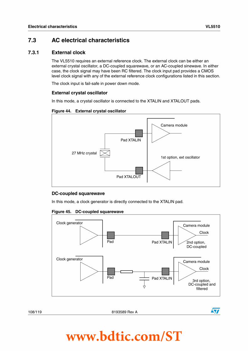
Electrical characteristics VL5510
108/119 8193589 Rev A
7.3 AC electrical characteristics
7.3.1 External clock
The VL5510 requires an external reference clock. The external clock can be either an external crystal oscillator, a DC-coupled squarewave, or an AC-coupled sinewave. In either case, the clock signal may have been RC filtered. The clock input pad provides a CMOS level clock signal with any of the external reference clock configurations listed in this section.
The clock input is fail-safe in power down mode.
External crystal oscillator
In this mode, a crystal oscillator is connected to the XTALIN and XTALOUT pads.
Figure 44. External crystal oscillator
DC-coupled squarewave
In this mode, a clock generator is directly connected to the XTALIN pad.
Figure 45. DC-coupled squarewave
Pad XTALOUT
Camera module
1st option, ext oscillator27 MHz crystal
Pad XTALIN
Pad
Clock
Clock generatorCamera module
3rd option, DC-coupled and
Pad Pad XTALIN
Clock
Clock generatorCamera module
2nd option,
Pad XTALIN
DC-coupled
filtered
www.bdtic.com/ST

VL5510 Electrical characteristics
8193589 Rev A 109/119
AC-coupled sinewave
In this mode, a clock generator is connected to the XTALIN pad through a band pass filter. The signal input is a sinewave.
Figure 46. AC-coupled sinewave
Clock input signal specification
7.3.2 Chip enable (CE)
XSHUTDOWN is a CMOS digital input. The module is powered down when a logic 0 is applied to CE.
7.3.3 I2C slave interface
VL5510 contains an I2C-type interface which uses two signals: a bidirectional serial data line (SDA) and an input-only serial clock line (SCL).
Table 31. Clock input signal specification
ClockRange
UnitMin. Typ. Max.
DC-coupled squarewave VDD V
AC-coupled sinewave 0.5 1 1.2 Vp-p
Clock frequency (normal operation)
6.56.50, 8.40, 9.60, 9.72, 12.00, 13.00,
16.80, 19.20, 19.44 27 27.7730 MHz
Pad
Clock
Clock generatorCamera module
3rd option,AC-coupled and filtered
Pad XTALIN
Table 32. Serial interface voltage levels
Parameter SymbolStandard mode Fast mode
UnitMin. Max. Min. Max.
Hysteresis of Schmitt trigger inputs Vhys(1) - - - - -
VDD > 2 V - N/A N/A 0.05 VDD - V
VDD < 2 V - N/A N/A 0.1 VDD - V
Low level output voltage (open drain) at 3 mA sink current
- - - - - -
VDD > 2 V VOL1 0 0.4 0 0.4 V
www.bdtic.com/ST

Electrical characteristics VL5510
110/119 8193589 Rev A
Figure 47. Voltage level specification
VDD < 2 V VOL3 N/A N/A 0 0.2 VDD V
High level output voltage VOH N/A N/A 0.8 VDD - V
Output fall time from VIHmin to VILmax with a bus capacitance from 10 pF to 400 pF
tof - 250 20 + 0.1Cb(2) 250 ns
Pulse width of spikes which must be suppressed by the input filter
tSP N/A N/A 0 50 ns
1. Maximum VIH = VDDmax + 0.5 V
2. Cb = capacitance of one bus line in pF
Table 32. Serial interface voltage levels (continued)
Parameter SymbolStandard mode Fast mode
UnitMin. Max. Min. Max.
VIH = 0.7 * VDD
VIL = 0.3 * VDD
VOH = 0.8 * VDD
VOL = 0.2 * VDD
Input voltage levels Output voltage levels
Table 33. Timing specification
Parameter SymbolStandard mode Fast mode
UnitMin. Max. Min. Max.
SCL clock frequency fSCL 0 100 0 400 kHz
Hold time for a repeated start tHD;STA 4.0 - 0.6 - µs
Low period of SCL tLOW 4.7 - 1.3 - µs
High period of SCL tHIGH 4.0 - 0.6 - µs
Set-up time for a repeated start tSU;STA 4.7 - 0.6 - µs
Data hold time(1) tHD;DAT 300 - 300 - ns
Data set-up time(1) tSU;DAT 250 - 100 - ns
Rise time of SCL and SDA tr - 1000 20+0.1Cb(2) 300 ns
Fall time of SCL and SDA tf - 300 20+0.1Cb(2) 300 ns
Set-up time for a stop tSU;STO 4.0 - 0.6 - µs
www.bdtic.com/ST
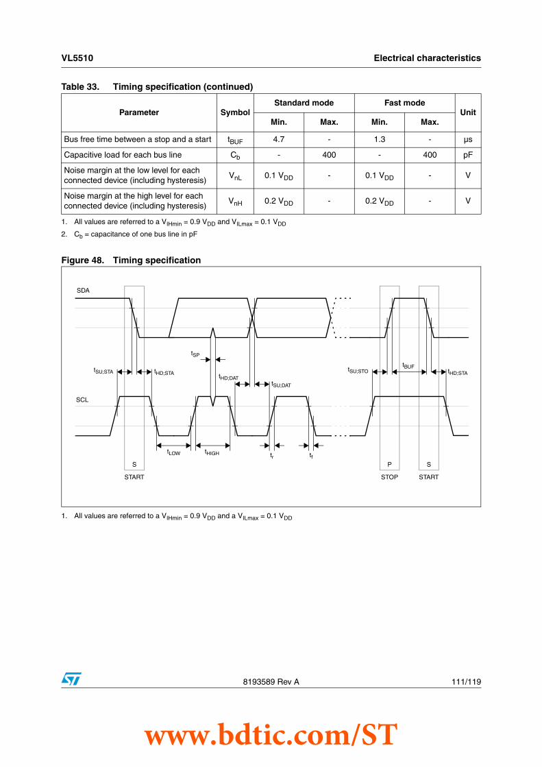
VL5510 Electrical characteristics
8193589 Rev A 111/119
Figure 48. Timing specification
1. All values are referred to a VIHmin = 0.9 VDD and a VILmax = 0.1 VDD
Bus free time between a stop and a start tBUF 4.7 - 1.3 - µs
Capacitive load for each bus line Cb - 400 - 400 pF
Noise margin at the low level for each connected device (including hysteresis)
VnL 0.1 VDD - 0.1 VDD - V
Noise margin at the high level for each connected device (including hysteresis)
VnH 0.2 VDD - 0.2 VDD - V
1. All values are referred to a VIHmin = 0.9 VDD and VILmax = 0.1 VDD
2. Cb = capacitance of one bus line in pF
Table 33. Timing specification (continued)
Parameter SymbolStandard mode Fast mode
UnitMin. Max. Min. Max.
SDA
SCL
START STOP START
tBUF
tLOW tHIGH
tHD;STA tHD;DATtSU;DAT
tSU;STA tSU;STO tHD;STA
tftr
tSP
S P S
www.bdtic.com/ST

Electrical characteristics VL5510
112/119 8193589 Rev A
Figure 49. SDA/SCL rise and fall times
7.3.4 Parallel data interface timings
The VL5510 contains a parallel data output port (D[11:0]), plus associated qualification signals (HSYNC, VSYNC, PCLK).
This port can be enabled and disabled (tri-stated) to facilitate multiple camera systems or bit-serial output configurations. The port is disabled (high impedance) upon reset.
Synchronization signals and clock signal polarity are fully programmable.
Figure 50. Parallel data output video timing
0.9 * VDD
0.1 * VDD
0.9 * VDD
0.1 * VDD
tftr
Table 34. Parallel data interface timings
Parameter symbol Parameter description Min Max Unit
fPCLK PCLK frequency - 27 MHz
tPCLKL PCLK low width 10 - ns
tPCLKH PCLK high width 10 - ns
tDV PCLK to output valid -5 5 ns
tPCLKPL tPCLKH
1/fPCLK
PCLK
DATA[0:7]HS, VS
polarity = 0
tDV
Valid
www.bdtic.com/ST

VL5510 Electrical characteristics
8193589 Rev A 113/119
7.3.5 CCP Tx interface timing
The following parameters below are measured across a terminated 100 Ω transmission line csi_signalling_mode register is set to 1, data/strobe mode.
Note: For further information on the CCP please refer to the following specification documents:SMIA 1.0 Part 2: CCP2 Specification 30-6-04.
Table 35. CCP interface - DATA+, DATA-, CLK+, CLK- characteristics
Symbol Parameter Min. Typ. Max. Unit
VOH Output voltage high(1)
1. Measured over a 100 W load.
- - 1475 mV
VOL Output voltage low(1) 925 - - mV
|VOD| Output differential voltage(1) 250 - 400 mV
VOS Output offset voltage(1) 1125 - 1275 mW
VCM Common mode voltage (self biasing) 1 1.2 1.4 V
RO Output Impedance 40 - 140 W
|ΔVOD| Change in |VOD| between A and B(1) - - 25 mV
ΔVOS Change in |VOS| between A and B(1) - - 25 mV
Isa, Isb Output current (Driver shorted to ground) - - 40 mA
Isab Output current (Driver shorted together) - - 12 mA
Table 36. CCP interface timing characteristics
Symbol Parameter Min. Max. Unit
Freq Max Frequency - 500 MHz
Clock Clock signal duty cycle (250 MHz) 40 60 %
Trise VOD Rise time, 20-80% 300 500 ps
Tfall VOD Fall time, 20-80% 300 500 ps
Tshew Total skew between signals - 100 ps
www.bdtic.com/ST

Package characteristics VL5510
114/119 8193589 Rev A
8 Package characteristics
8.1 Lead-free packagesIn order to meet environmental requirements, ST offers this device in different grades of ECOPACK® package, depending on their level of environmental compliance. ECOPACK® specifications, grade definitions and product status are available at: www.st.com. ECOPACK® is an ST trademark.
8.2 Ordering information
8.3 OLGA packageThe proposed production package is an OLGA (organic land grid array). This organic substrate is designed to fit with a 12 mm x 12 mm package with 0.5 lead pitch. The substrate enables the interconnection between the Die and the package pins.
Figure 51 gives a description of the OLGA package used for the VL5510.
Table 37. Ordering information
Order code Package
VL5510-die1 Bare die
VL5510-BLGA OLGA
www.bdtic.com/ST

VL5510 Package characteristics
8193589 Rev A 115/119
Figure 51. OLGA package pinout
Table 38 gives the signal assignment on the OLGA package.
Table 38. OLGA pinout
Name OLGA pin Name OLGA pin
VH3V6DAC 56 VDD_2V5 15
VDD_3V3 11 VDD_3V3 49
VDD_1V2 10 VDD_1V2 18
AVDD 9 AVDD 53
AVSS 8 AVSS 52
DGND 12 DGND 14
AVDD_PLL 20 AVSS_PLL 19
DOUT1P
DOUT1N
DOUT0P
DOUT0NCKOUTP
CKOUTN
DIO0
DIO1
PCLK
DIO2
DIO4
DIO5
DIO6
DIO7
DIO8
DIO9
DIO10
SD
A
PO
RT
ES
T
PO
RS
GN
TD
0T
D1
TM
S
TC
K
AV
SS
-0
AV
DD
-0
VD
D_1V
2-N
VD
D_3V
3-N
DG
ND
-N
DG
ND
-S
VD
D_2V
5
XTA
LIN
XTA
LOU
T
VD
D_1V
2-S
AV
SS
_PLL
AV
DD
_PLL
Pin # 1 ID
DIO3
SCL
SLCLK
SLMOSI
SLMISOSLCS
MODE0
MODE1
MODE2
SCLK
MISO
MOSI
SS1
SS3
ATEST1
ATEST0
RSTHIPAD
VBLKREFAZPAD
VRSTLOPAD
VRTRSTLOPAD
SS2
VD
AC
LOPA
D
VR
TS
F2V
5
VD
AC
HI
VS
IGH
IPAD
VH
3V6D
AC
AV
DA
CPA
D
VH
4V0C
P
AV
DD
-N
AV
SS
-N
VD
D_3V
3-S
VD
D_3V
3-E
VD
D_1V
2-E
HV
XS
HU
TD
OW
N
VS
YN
C
HS
YN
C
DIO
11
DG
ND
-E
Bottom by top trough view
120
21
40
6041
80
61
www.bdtic.com/ST

Package characteristics VL5510
116/119 8193589 Rev A
DOUT1N 22 DOUT1P 21
DOUT0N 24 DOUT0P 23
CKOUTN 26 CKOUTP 25
XTALOUT 17 XTALIN 16
MODE2 73 MODE1 74
MODE0 75 MISO 71
SS3 67 SS2 68
SS1 69 MOSI 70
SCLK 72 SLMISO 77
SLCS 76 SLMOSI 78
SLCLK 79 TDO 4
TMS 6 TDI 5
TCK 7 VSYNC 43
HSYNC 42 PCLK 31
DIO11 41 DIO10 40
DIO9 39 DIO8 38
DIO7 37 DIO6 36
DIO5 35 DIO4 34
DIO3 33 DIO2 32
DIO1 30 DIO0 29
SDA 1 SCL 80
XSHUTDOWN 44 HV 45
VH4V0CP 54 AVDACPAD 55
VRTSF2V5 59 VSIGHIPAD 57
VDACHI 58 ATEST1 66
ATEST0 65 VBLKREFAZPAD 63
VRTRSTLOPAD 60 VDACLOPAD 60
VRSTLOPAD 62 RSTHIPAD 64
PORSGN 3 PORTEST 2
DGND 48 VDD_3V3 47
VDD_1V2 46 Unconnected 13, 50, 51
Table 38. OLGA pinout (continued)
Name OLGA pin Name OLGA pin
www.bdtic.com/ST

VL5510 Package characteristics
8193589 Rev A 117/119
Figure 52 gives the OLGA package outline and mechanical data.
Figure 52. OLGA 80-pin lead pitch package outline and mechanical data
www.bdtic.com/ST

Revision history VL5510
118/119 8193589 Rev A
9 Revision history
Table 39. Document revision history
Date Revision Changes
05-May-2009 A Initial release
www.bdtic.com/ST

VL5510
8193589 Rev A 119/119
Please Read Carefully:
Information in this document is provided solely in connection with ST products. STMicroelectronics NV and its subsidiaries (“ST”) reserve theright to make changes, corrections, modifications or improvements, to this document, and the products and services described herein at anytime, without notice.
All ST products are sold pursuant to ST’s terms and conditions of sale.
Purchasers are solely responsible for the choice, selection and use of the ST products and services described herein, and ST assumes noliability whatsoever relating to the choice, selection or use of the ST products and services described herein.
No license, express or implied, by estoppel or otherwise, to any intellectual property rights is granted under this document. If any part of thisdocument refers to any third party products or services it shall not be deemed a license grant by ST for the use of such third party productsor services, or any intellectual property contained therein or considered as a warranty covering the use in any manner whatsoever of suchthird party products or services or any intellectual property contained therein.
UNLESS OTHERWISE SET FORTH IN ST’S TERMS AND CONDITIONS OF SALE ST DISCLAIMS ANY EXPRESS OR IMPLIEDWARRANTY WITH RESPECT TO THE USE AND/OR SALE OF ST PRODUCTS INCLUDING WITHOUT LIMITATION IMPLIEDWARRANTIES OF MERCHANTABILITY, FITNESS FOR A PARTICULAR PURPOSE (AND THEIR EQUIVALENTS UNDER THE LAWSOF ANY JURISDICTION), OR INFRINGEMENT OF ANY PATENT, COPYRIGHT OR OTHER INTELLECTUAL PROPERTY RIGHT.
UNLESS EXPRESSLY APPROVED IN WRITING BY AN AUTHORIZED ST REPRESENTATIVE, ST PRODUCTS ARE NOTRECOMMENDED, AUTHORIZED OR WARRANTED FOR USE IN MILITARY, AIR CRAFT, SPACE, LIFE SAVING, OR LIFE SUSTAININGAPPLICATIONS, NOR IN PRODUCTS OR SYSTEMS WHERE FAILURE OR MALFUNCTION MAY RESULT IN PERSONAL INJURY,DEATH, OR SEVERE PROPERTY OR ENVIRONMENTAL DAMAGE. ST PRODUCTS WHICH ARE NOT SPECIFIED AS "AUTOMOTIVEGRADE" MAY ONLY BE USED IN AUTOMOTIVE APPLICATIONS AT USER’S OWN RISK.
Resale of ST products with provisions different from the statements and/or technical features set forth in this document shall immediately voidany warranty granted by ST for the ST product or service described herein and shall not create or extend in any manner whatsoever, anyliability of ST.
ST and the ST logo are trademarks or registered trademarks of ST in various countries.
Information in this document supersedes and replaces all information previously supplied.
The ST logo is a registered trademark of STMicroelectronics. All other names are the property of their respective owners.
© 2009 STMicroelectronics - All rights reserved
STMicroelectronics group of companies
Australia - Belgium - Brazil - Canada - China - Czech Republic - Finland - France - Germany - Hong Kong - India - Israel - Italy - Japan - Malaysia - Malta - Morocco - Philippines - Singapore - Spain - Sweden - Switzerland - United Kingdom - United States of America
www.st.com
www.bdtic.com/ST