high efficiency step-down controller with embedded … · high efficiency step-down controller with...
TRANSCRIPT

February 2008 Rev 1 1/48
PM6675ASHigh efficiency step-down controller
with embedded 2 A LDO regulator
Features Switching section
– 4.5 V to 36 V input voltage range – 0.6 V, ±1 % voltage reference – Selectable 1.5 V fixed output voltage– Adjustable 0.6 V to 3.3 V output voltage– 1.237 V ±1 % reference voltage available– Very fast load transient response using
constant-on-time control loop – No RSENSE current sensing using low side
MOSFETs' RDS(ON) – Negative current limit– Latched OVP and UVP– Soft-start internally fixed at 3 ms– Selectable pulse skipping at light load– Selectable No-audible (33 kHz) pulse skip
mode – Ceramic output capacitors supported– Output voltage ripple compensation– Output soft-end
LDO regulator section – Adjustable 0.6 V to 3.3 V output voltage – Selectable ±1 Apk or ±2 Apk current limit– Dedicated power-good signal– Ceramic output capacitors supported– Output soft-end
Applications Industrial application on 24 V
Graphic cards
Embedded computer systems
DescriptionThe PM6675AS device consists of a single high efficiency step-down controller and an independent low drop-out (LDO) linear regulator.
The constant on-time (COT) architecture assures fast transient response supporting both electrolytic and ceramic output capacitors. An embedded integrator control loop compensates the DC voltage error due to the output ripple.
Selectable low-consumption mode allows the highest efficiency over a wide range of load conditions. The low-noise mode sets the minimum switching frequency to 33 kHz for audio-sensitive applications. The LDO linear regulator can sink and source up to 2 Apk. Two fixed current limit(±1 A- ±2 A) can be chosen.
An active soft-end is independently performed on both the switching and the linear regulators outputs when disabled.
VFQFPN-24 4x4
Table 1. Device summary
Order codes Package Packaging
PM6675ASVFQFPN-24 4x4 (exposed pad)
Tube
PM6675ASTR Tape and reel
www.st.com

Contents PM6675AS
2/48
Contents
1 Typical application circuit . . . . . . . . . . . . . . . . . . . . . . . . . . . . . . . . . . . . 4
2 Pin settings . . . . . . . . . . . . . . . . . . . . . . . . . . . . . . . . . . . . . . . . . . . . . . . . 5
2.1 Connections . . . . . . . . . . . . . . . . . . . . . . . . . . . . . . . . . . . . . . . . . . . . . . . . 5
2.2 Pin description . . . . . . . . . . . . . . . . . . . . . . . . . . . . . . . . . . . . . . . . . . . . . . 6
3 Electrical data . . . . . . . . . . . . . . . . . . . . . . . . . . . . . . . . . . . . . . . . . . . . . . 8
3.1 Maximum rating . . . . . . . . . . . . . . . . . . . . . . . . . . . . . . . . . . . . . . . . . . . . . 8
3.2 Thermal data . . . . . . . . . . . . . . . . . . . . . . . . . . . . . . . . . . . . . . . . . . . . . . . 8
3.3 Recommended operating conditions . . . . . . . . . . . . . . . . . . . . . . . . . . . . . 8
4 Electrical characteristics . . . . . . . . . . . . . . . . . . . . . . . . . . . . . . . . . . . . . 9
5 Block diagram . . . . . . . . . . . . . . . . . . . . . . . . . . . . . . . . . . . . . . . . . . . . . 12
6 Typical operating characteristics . . . . . . . . . . . . . . . . . . . . . . . . . . . . . 13
7 Device description . . . . . . . . . . . . . . . . . . . . . . . . . . . . . . . . . . . . . . . . . 16
7.1 Switching section - constant on-time pwm controller . . . . . . . . . . . . . . . . 16
7.1.1 Constant-on-time architecture . . . . . . . . . . . . . . . . . . . . . . . . . . . . . . . . 18
7.1.2 Output ripple compensation and loop stability . . . . . . . . . . . . . . . . . . . . 19
7.1.3 Pulse-skip and no-audible pulse-skip modes . . . . . . . . . . . . . . . . . . . . . 24
7.1.4 Mode-of-operation selection . . . . . . . . . . . . . . . . . . . . . . . . . . . . . . . . . 26
7.1.5 Current sensing and current limit . . . . . . . . . . . . . . . . . . . . . . . . . . . . . . 27
7.1.6 POR, UVLO and soft-start . . . . . . . . . . . . . . . . . . . . . . . . . . . . . . . . . . . 28
7.1.7 Switching section power-good signal . . . . . . . . . . . . . . . . . . . . . . . . . . . 29
7.1.8 Switching section output discharge . . . . . . . . . . . . . . . . . . . . . . . . . . . . 29
7.1.9 Gate drivers . . . . . . . . . . . . . . . . . . . . . . . . . . . . . . . . . . . . . . . . . . . . . . 30
7.1.10 Reference voltage and bandgap . . . . . . . . . . . . . . . . . . . . . . . . . . . . . . 30
7.1.11 Switching section OV and UV protections . . . . . . . . . . . . . . . . . . . . . . . 30

PM6675AS Contents
3/48
7.1.12 Device thermal protection . . . . . . . . . . . . . . . . . . . . . . . . . . . . . . . . . . . 31
7.2 LDO linear regulator section . . . . . . . . . . . . . . . . . . . . . . . . . . . . . . . . . . . 31
7.2.1 LDO section current limit . . . . . . . . . . . . . . . . . . . . . . . . . . . . . . . . . . . . 32
7.2.2 LDO section soft-start . . . . . . . . . . . . . . . . . . . . . . . . . . . . . . . . . . . . . . 33
7.2.3 LDO section power-good signal . . . . . . . . . . . . . . . . . . . . . . . . . . . . . . . 33
7.2.4 LDO section output discharge . . . . . . . . . . . . . . . . . . . . . . . . . . . . . . . . 33
8 Application information . . . . . . . . . . . . . . . . . . . . . . . . . . . . . . . . . . . . . 34
8.1 External components selection . . . . . . . . . . . . . . . . . . . . . . . . . . . . . . . . 34
8.1.1 Inductor selection . . . . . . . . . . . . . . . . . . . . . . . . . . . . . . . . . . . . . . . . . . 35
8.1.2 Input capacitor selection . . . . . . . . . . . . . . . . . . . . . . . . . . . . . . . . . . . . 37
8.1.3 Output capacitor selection . . . . . . . . . . . . . . . . . . . . . . . . . . . . . . . . . . . 38
8.1.4 MOSFETs selection . . . . . . . . . . . . . . . . . . . . . . . . . . . . . . . . . . . . . . . . 39
8.1.5 Diode selection . . . . . . . . . . . . . . . . . . . . . . . . . . . . . . . . . . . . . . . . . . . 41
8.1.6 VOUT current limit setting . . . . . . . . . . . . . . . . . . . . . . . . . . . . . . . . . . . 41
8.1.7 All ceramic capacitors application . . . . . . . . . . . . . . . . . . . . . . . . . . . . . 42
9 Package mechanical data . . . . . . . . . . . . . . . . . . . . . . . . . . . . . . . . . . . . 45
10 Revision history . . . . . . . . . . . . . . . . . . . . . . . . . . . . . . . . . . . . . . . . . . . 47

Typical application circuit PM6675AS
4/48
1 Typical application circuit
Figure 1. Application circuit
VLDO
VSMPS
+5VR LP
VLDOINHGATE
PHASE
LGATE
CSNS
PGND
VSNS
VSEL
LIN
LPG
LOUT
LFB
LGND
LILI
M
AVC
C
VCC
VOS
CBOOTN
OS
KIP
SPG LE
N
SWE
N
VR
EF
CO
MP
SGN
D
VIN
L
R1
C IN
C INT
C IN4
C OUT
C BYP
C OUT2
C IN2C IN3
1
2
24
4
23
10
9
16
19
17
20
21
3 12 6 18 8 22
5 15 14 13 7 11
R2
C BOOT
R LIM
LDO PG
SMPS PG
PM6675AVLDO
VSMPS
+5VR LPR LP
VLDOINHGATE
PHASE
LGATE
CSNS
PGND
VSNS
VSEL
LIN
LPG
LOUT
LFB
LGND
LILI
M
AVC
C
VCC
VOS
CBOOTN
OS
KIP
SPG LE
N
SWE
N
VR
EF
CO
MP
SGN
D
VIN
L
R1
C INC IN
C INTC INT
C IN4C IN4
C OUTC OUT
C BYPC BYP
C OUT2C OUT2
C IN2C IN3C IN3
1
2
24
4
23
10
9
16
19
17
20
21
3 12 6 18 8 22
5 15 14 13 7 11
R2
C BOOT
R LIMR LIM
LDO PG
SMPS PG
PM6675APM6675AS

PM6675AS Pin settings
5/48
2 Pin settings
2.1 Connections
Figure 2. Pin connection (through top view)
PHA
SE
HG
ATE
PM6675A
1
67 12
13
181924
VREF
VOSC
VSN
S
CO
MP
LILI
MC
SNS
BO
OT
LIN
LOU
T
SWEN
LEN
SPG
PGND
LGATE
VCC
VSEL
LGND
LFB
LPG
NOSKIP
SGND
AVCCPH
ASE
HG
ATE
PM6675A
1
67 12
13
181924
VREF
VOSC
VSN
S
CO
MP
LILI
MC
SNS
BO
OT
LIN
LOU
T
SWEN
LEN
SPG
PGND
LGATE
VCC
PHA
SE
HG
ATE
PM6675A
1
67 12
13
181924
VREF
VOSC
VSN
S
CO
MP
LILI
MC
SNS
BO
OT
LIN
LOU
T
PM6675A
1
67 12
13
181924
VREF
VOSC
VSN
S
CO
MP
LILI
MC
SNS
BO
OT
LIN
LOU
T
SWEN
LEN
SPG
PGND
LGATE
VCC
VSEL
LGND
LFB
LPG
NOSKIP
SGND
AVCC
VSEL
LGND
LFB
LPG
NOSKIP
SGND
AVCC
PM6675AS
Pin settings PM6675AS
6/48
2.2 Pin description
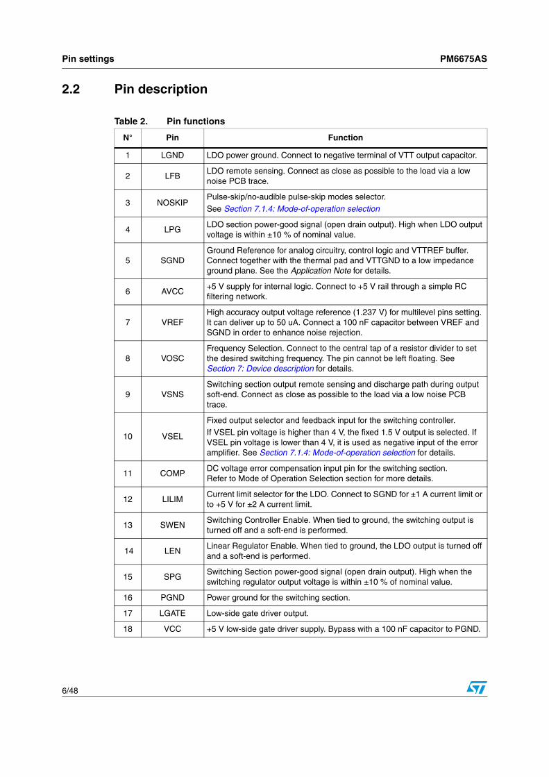
Table 2. Pin functions
N° Pin Function
1 LGND LDO power ground. Connect to negative terminal of VTT output capacitor.
2 LFBLDO remote sensing. Connect as close as possible to the load via a low noise PCB trace.
3 NOSKIPPulse-skip/no-audible pulse-skip modes selector.
See Section 7.1.4: Mode-of-operation selection
4 LPGLDO section power-good signal (open drain output). High when LDO output voltage is within ±10 % of nominal value.
5 SGNDGround Reference for analog circuitry, control logic and VTTREF buffer. Connect together with the thermal pad and VTTGND to a low impedance ground plane. See the Application Note for details.
6 AVCC+5 V supply for internal logic. Connect to +5 V rail through a simple RC filtering network.
7 VREFHigh accuracy output voltage reference (1.237 V) for multilevel pins setting. It can deliver up to 50 uA. Connect a 100 nF capacitor between VREF and SGND in order to enhance noise rejection.
8 VOSCFrequency Selection. Connect to the central tap of a resistor divider to set the desired switching frequency. The pin cannot be left floating. See Section 7: Device description for details.
9 VSNSSwitching section output remote sensing and discharge path during output soft-end. Connect as close as possible to the load via a low noise PCB trace.
10 VSEL
Fixed output selector and feedback input for the switching controller. If VSEL pin voltage is higher than 4 V, the fixed 1.5 V output is selected. If VSEL pin voltage is lower than 4 V, it is used as negative input of the error amplifier. See Section 7.1.4: Mode-of-operation selection for details.
11 COMPDC voltage error compensation input pin for the switching section.Refer to Mode of Operation Selection section for more details.
12 LILIMCurrent limit selector for the LDO. Connect to SGND for ±1 A current limit or to +5 V for ±2 A current limit.
13 SWENSwitching Controller Enable. When tied to ground, the switching output is turned off and a soft-end is performed.
14 LENLinear Regulator Enable. When tied to ground, the LDO output is turned off and a soft-end is performed.
15 SPGSwitching Section power-good signal (open drain output). High when the switching regulator output voltage is within ±10 % of nominal value.
16 PGND Power ground for the switching section.
17 LGATE Low-side gate driver output.
18 VCC +5 V low-side gate driver supply. Bypass with a 100 nF capacitor to PGND.

PM6675AS Pin settings
7/48
19 CSNSCurrent sense input for the switching section. This pin must be connected through a resistor to the drain of the synchronous rectifier (RDSon sensing) to set the current limit threshold.
20 PHASE Switch node connection and return path for the high side gate driver.
21 HGATE High-Side Gate Driver Output
22 BOOTBootstrap capacitor connection. Input for the supply voltage of the high-side gate driver.
23 LINLinear Regulator Input. Bypass to LGND by a 10 µF ceramic capacitor for noise rejection enhancement.
24 LOUTLDO linear regulator output. Bypass with a 20 µF (2x10 µF MLCC) filter capacitor.
Table 2. Pin functions (continued)
N° Pin Function

Electrical data PM6675AS
8/48
3 Electrical data
3.1 Maximum rating
3.2 Thermal data
3.3 Recommended operating conditions
Table 3. Absolute maximum ratings (1)
1. Free air operating conditions unless otherwise specified. Stresses beyond those listed under "absolute maximum ratings" may cause permanent damage to the device. Exposure to absolute maximum rated conditions for extended periods may affect device reliability.
Symbol Parameter Value Unit
VAVCC AVCC to SGND -0.3 to 6
V
VVCC VCC to SGND -0.3 to 6
PGND, LGND to SGND -0.3 to 0.3
HGATE and BOOT to PHASE -0.3 to 6
HGATE and BOOT to PGND -0.3 to 44
VPHASE PHASE to SGND -0.3 to 38
LGATE to PGND -0.3 to VVCC +0.3
CSNS, SPG, LEN, SWEN, LILIM, COMP, VSEL, VSNS, VOSC, VREF, NOSKIP to SGND
-0.3 to VAVCC + 0.3
LPG,VREF, LOUT, LFB to SGND -0.3 to VAVCC + 0.3
LIN, LOUT, LPG, LIN to LGND -0.3 to VAVCC + 0.3
PTOT Power dissipation @TA = 25°C 2.3 W
Table 4. Thermal data
Symbol Parameter Value Unit
RthJA Thermal resistance junction to ambient 42 °C/W
TSTG Storage temperature range -50 to 150
°CTA Operating ambient temperature range -40 to 85
TJ Junction operating temperature range -40 to 125
Table 5. Recommended operating conditions
Symbol Parameter Min Typ Max Unit
VIN Input voltage range 4.5 36
VVAVCC IC supply voltage 4.5 5.5
VVCC IC supply voltage 4.5 5.5

PM6675AS Electrical characteristics
9/48
4 Electrical characteristics
Table 6. Electrical characteristics TA = - 25 °C to 85 °C , VCC = AVCC = +5 V, LIN = 1.5 V and LOUT= 0.6 V if not otherwise specified (1).
Symbol Parameter Test condition Min Typ Max Unit
Supply section
IINOperating current
(Switching + LDO)
SWEN, LEN, VSEL and NOSKIP connected to AVCC, No load on LOUT output.
2
mA
ISW Operating current (switching)SWEN, VSEL and NOSKIP connected to AVCC, LEN coneected to SGND.
1
ISHDN Shutdown operating current SWEN and LEN tied to SGND. 10 µA
UVLO
AVCC Under Voltage Lockout upper threshold
4.1 4.25 4.4
VAVCC Under Voltage Lockout lower threshold
3.85 4.0 4.1
UVLO hysteresis 70 mV
On-time (SMPS)
tON On-time durationVSEL low, NOSKIP low,
VVSNS = 2 V
VOSC = 300 mV 530 630 730ns
VOSC = 500 mV 320 380 440
OFF-TIME (SMPS)
tOFFMIN Minimum Off-Time 300 350 ns
Voltage reference
Voltage accuracy 4.5 V< VIN < 36 V 1.224 1.237 1.249 V
Load regulation -50 µA < IVREF < 50 µA -4 4
mVUndervoltage Lockout Fault Threshold
800
SMPS output
VOUT SMPS fixed output voltageVSEL connected to AVCC, NOSKIP tied to SGND, No Load
1.5 V
Feedback output voltage accuracy
-1.5 1.5 %

Electrical characteristics PM6675AS
10/48
Table 6. Electrical characteristics (continued)TA = -25 °C to 85 °C , VCC = AVCC = +5 V, LIN = 1.5 V and LOUT= 0.6 V if not otherwise specified. (1)
Symbol Parameter Test condition Min Typ Max Unit
Current limit and zero crossing comparator
ICSNS CSNS input bias current 90 100 110 µA
Comparator offset -6 6
mV
Positive current limit threshold VPGND - VCSNS 100
fixed negative current limit
threshold110
VZC,OFFS Zero crossing comparator offset -11 -5 1
High and low side gate drivers
HGATE driver on-resistanceHGATE high state (pullup) 2.0 3
ΩHGATE low state (pulldown) 1.8 2.7
LGATE driver on-resistanceLGATE high state (pullup) 1.4 2.1
LGATE low state (pulldown) 0.6 0.9
UVP/OVP protections and PGOOD signals
OVP Over voltage threshold 112 115 118
%
UVP Under voltage threshold 67 70 73
PGOOD
SMPS upper threshold 107 110 113
SMPS lower threshold 86 90 93
LDO upper threshold 107 110 113
LDO lower threshold 86 90 93
IPG,LEAK SPG and LPG leakeage current SPG and LPG forced to 5.5 V 1 µA
VPG,LOW SPG and LPG low level voltage ILPG,SINK = ISPG,SINK = 4 mA 150 250 mV
Soft-start section (SMPS)
Soft-start ramp time
(4 steps current limit)2 3 4 ms
Soft-start current limit step 25 µA
Soft end section
Switching section discharge resistance
15 25 35Ω
LDO section discharge resistance 15 25 35
LDO section
VLREF
LDO reference voltage 600
mVLDO output accuracy respect to VREF
-1 mA < ILDO < 1 mA -20 20
-1 A < ILDO < 1 A -25 25

PM6675AS Electrical characteristics
11/48
Symbol Parameter Test condition Min Typ Max Unit
ILDO,CL
LDO sink current limitVLFB > VLREF , LILIM = 5 V -3 -2.3 -2
A
VLFB > VLREF, LILIM = 0 V -1.6 -1.3 -1
LDO source current limit
0.9 ⋅ VLREF < VLFB < VLREF, LILIM=5V
2 2.4 3
0.9 ⋅ VLREF < VLFB < VLREF,LILIM = 0 V
1 1.3 1.6
VLFB < 0.9 ⋅ VLREF, LILIM = 5 V 1 1.3 1.6
VLFB < 0.9 ⋅ VLREF, LILIM = 0 V 0.5 0.8 1.1
ILIN,BIAS LDO input bias current, on LEN connected to AVCC, no load 1 10
µA
LDO input bias current, off LEN = 0 V, no load 1
ILFB,BIAS LFB input bias currentLEN connected to AVCC
VLFB = 0.6 V-1 1
ILFB,LEAK LFB leakage current LEN=0V, VLFB = 0.6V -1 1
Power management section
VVTHVSEL VSEL pin thresholds
Fixed modeVAVCC -0.7
V
Adjustable modeVAVCC -1.3
VVTHNOSKIP NOSKIP pin thresholds
Forced-PWM modeVAVCC -0.8
No-audible mode 1.0VAVCC -1.5
Pulse-skip mode 0.5
VVTHLEN,VVTHSWEN
LEN, SWEN turn off level 0.4
LEN, SWEN turn on level 1.6
VVTHLILIM LILIM pin thresholds±2A LDO current limit
VAVCC -0.8
±1A LDO current limit 0.5
IIN,LEAK Logic input leakage current LEN, SWEN and LILIM = 5 V 10
µAIIN3,LEAK Multilevel input leakage current VSEL and NOSKIP = 5 V 10
IOSC,LEAK VOSC pin leakage current VOSC = 1 V 1
Thermal shutdown
TSHDN Shutdown temperature (2) 150 °C
1. Specifications referred to TJ = TA. All the parameters at operating temperatures extremes are guaranteed by design and statistical correlation (not production tested).
2. Guaranteed by design. Not production tested.
Table 6. Electrical characteristics (continued)TA = -25 °C to 85 °C , VCC = AVCC = +5 V, LIN = 1.5 V and LOUT= 0.6 V if not otherwise specified. (1)
Block diagram PM6675AS
12/48
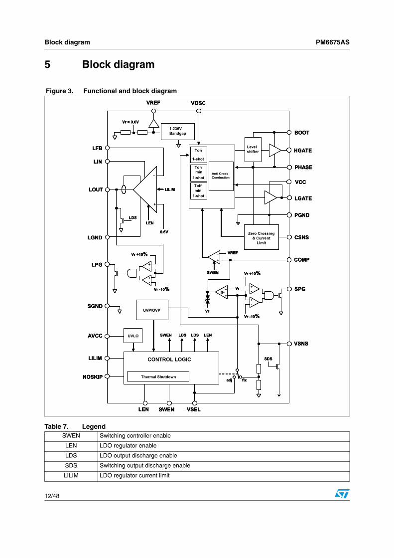
5 Block diagram
Figure 3. Functional and block diagram
LOUT
LIN
LPG
VCC
AVCC
SGND
VSELLEN SWEN
CSNS
HGATE
LGATE
PHASE
BOOT
PGND
NOSKIP
VREF
VSNS
LFB
VOSC
COMP
CONTROL LOGIC
Zero Crossing & Current
Limit
SPG
Vr -10%
Vr +10%
+-
+-
gm+
_ Vr
+
_ VREF
Level shifter
1.236V Bandgap
Vr = 0.6V
SDS
LDS
LEN
LEN
LILIM
UVLO
SWEN
SWEN
Vr
Ton
Toff
1-shot
1-shot
1-shot
fixadj
UVP/OVP
Thermal Shutdown
min
min
+-
+-
Vr +10%
Vr -10%
0.6V
+
_
Ton
Anti Cross Conduction
LILIM
LGND
LDS
LDS
LOUT
LIN
LPG
VCC
AVCC
SGND
VSELLEN SWEN
CSNS
HGATE
LGATE
PHASE
BOOT
PGND
NOSKIP
VREF
VSNS
LFB
VOSC
COMP
CONTROL LOGIC
Zero Crossing & Current
Limit
SPG
Vr -10%
Vr +10%
+-
+-
gm+
_ Vr
+
_ VREF
Level shifter
1.236V Bandgap
Vr = 0.6V
SDS
LDS
LEN
LEN
LILIM
UVLO
SWEN
SWEN
Vr
Ton
Toff
1-shot
1-shot
1-shot
fixadj
UVP/OVP
Thermal Shutdown
min
min
+-
+-
Vr +10%
Vr -10%
0.6V
+
_
Ton
Anti Cross Conduction
LILIM
LGND
LDS
LDS
Table 7. Legend SWEN Switching controller enable
LEN LDO regulator enable
LDS LDO output discharge enable
SDS Switching output discharge enable
LILIM LDO regulator current limit
PM6675AS Typical operating characteristics
13/48
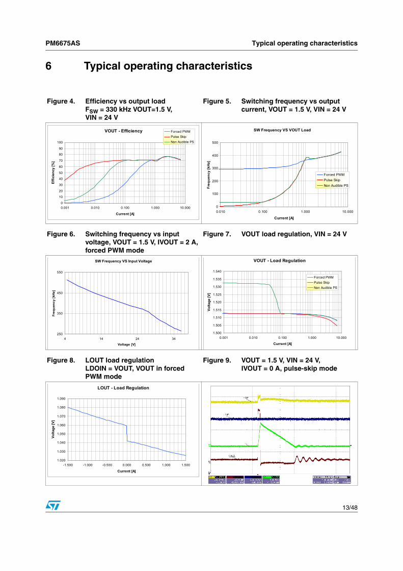
6 Typical operating characteristics
Figure 4. Efficiency vs output load
FSW = 330 kHz VOUT=1.5 V, VIN = 24 V
Figure 5. Switching frequency vs output current, VOUT = 1.5 V, VIN = 24 V
Figure 6. Switching frequency vs input voltage, VOUT = 1.5 V, IVOUT = 2 A, forced PWM mode
Figure 7. VOUT load regulation, VIN = 24 V
Figure 8. LOUT load regulation LDOIN = VOUT, VOUT in forced PWM mode
Figure 9. VOUT = 1.5 V, VIN = 24 V, IVOUT = 0 A, pulse-skip mode
VOUT - Efficiency
0
10
20
30
40
50
60
70
80
90
100
0.001 0.010 0.100 1.000 10.000
Current [A]
Effic
ienc
y [%
]
Forced PWMPulse SkipNon Audible PS
SW Frequency VS VOUT Load
0
100
200
300
400
500
0.010 0.100 1.000 10.000
Current [A]
Freq
uenc
y [k
Hz]
Forced PWMPulse SkipNon Audible PS
SW Frequency VS Input Voltage
250
350
450
550
4 14 24 34
Voltage [V]
Freq
uenc
y [k
Hz]
VOUT - Load Regulation
1.500
1.505
1.510
1.515
1.520
1.525
1.530
1.535
1.540
0.001 0.010 0.100 1.000 10.000
Current [A]
Volta
ge [V
]
Forced PWMPulse SkipNon Audible PS
LOUT - Load Regulation
1.020
1.030
1.040
1.050
1.060
1.070
1.080
1.090
-1.500 -1.000 -0.500 0.000 0.500 1.000 1.500
Current [A]
Volta
ge [V
]

Typical operating characteristics PM6675AS
14/48
Figure 10. VOUT = 1.5V , VIN = 24V, IVOUT = 0 A, forced-PWM mode
Figure 11. VOUT = 1.5 V, VIN = 24 V, no load, Non-audible pulse-skip mode(33 kHz)
Figure 12. VOUT Soft-start @150mΩ load, pulse-skip mode
Figure 13. LOUT turn on, VOUT in pulse-skip mode
Figure 14. VOUT Load Transient (VIN = 24 V, LOAD = 0 A -> 7 A @2.5 A/µs). pulse-skip mode
Figure 15. LOUT load transient (VIN = 24 V, LOAD = -1.5 A -> 1.5 A @2.5 A/µs). pulse-skip mode

PM6675AS Typical operating characteristics
15/48
Figure 16. VOUT and LOUT output voltages. VOUT soft-end. LOUT powered by an auxiliary rail
Figure 17. VOUT and LOUT output voltages LOUT soft-end
Figure 18. UV protection, pulse-skip mode LOUT powered by an auxiliary rail
Figure 19. OV protection, pulse-skip mode
Figure 20. VOUT current limit protection during a load transient (0 A to 9 A @2.5A/µs)
Figure 21. LOUT current limit during an output short

Device description PM6675AS
16/48
7 Device description
The PM6675AS combines a single high efficiency step-down controller and an independent Low Drop-Out (LDO) linear regulator in the same package.
The switching controller section is a high-performance, pseudo-fixed frequency, Constant-On-Time (COT) based regulator specifically designed for handling fast load transient over a wide range of input voltage.
The switching section output can be easily set to a fixed 1.5 V voltage without additional components or adjusted in the 0.6 V to 3.3 V range using an external resistor divider. The Switching Mode Power Supply (SMPS) can handle different modes of operation in order to minimize noise or power consumption, depending on the application needs. Selectable low-consumption and low-noise modes allow the highest efficiency and a 33 kHz minimum switching frequency respectively at light loads.
The current sensing is lossless, based on the Low-Side MOSFET turn-on resistance.
The input of the LDO can be either the switching section output or a lower voltage rail in order to reduce the total power dissipation. Linear regulator stability is achieved by filtering its output with a ceramic capacitor (20 µF or greater). The LDO linear regulator can sink and source up to 2 Apk.
Two fixed current limit (±1A-±2A) can be chosen.
An active soft-end is independently performed on both the switching and the linear regulators outputs when disabled.
7.1 Switching section - constant on-time pwm controllerThe PM6675AS employes a pseudo-fixed frequency, Constant On-Time (COT) controller as the core of the switching section. As well known, the COT controller concerns of a relatively simple algorithm and uses the ripple voltage derived across the output capacitor ESR to trigger the On-Time one-shot generator. In this way, the output capacitor ESR acts as a current sense resistor providing the appropriate ramp signal to the PWM comparator. Nearly constant switching frequency is achieved by the system loop in steady-state operating conditions by varying the On-Time duration, avoiding thus the need for a clock generator. The On-Time one shot duration is directly proportional to the output voltage, sensed at VSNS pin, and inversely proportional to the input voltage, sensed at the VOSC pin, as follows:
Equation 1
where KOSC is a constant value (130 ns typ.) and τ is the internal propagation delay (40ns typ.). The one-shot generator directly drives the high-side MOSFET at the beginning of each switching cycle allowing the inductor current to increase; after the On-Time has expired, an Off-Time phase, in which the low-side MOSFET is turned on, follows.
τ+=OSC
SNSOSCON V
VKT

PM6675AS Device description
17/48
The Off-Time duration is solely determined by the output voltage: when lower than the set value (i.e. the voltage at VSNS pin is lower than the internal reference = 0.6 V), the synchronous rectifier is turned off and a new cycle begins (Figure 22).
Figure 22. Inductor current and output voltage in steady state conditions
The duty-cycle of the buck converter is, in steady-state conditions, given by
Equation 2
The switching frequency is thus calculated as
Equation 3
where
Equation 4 a
Equation 4 b
Ton Toff
Inductor current
t
Output voltage
Vreg
IN
OUT
V
VD =
OSCOUT
OSC
OSC
SNSOSC
IN
OUT
ONSW K
1
V
VK
V
V
TD
f ⋅αα
===
IN
OSCOSC V
V=α
OUT
SNSOUT V
V=α
Device description PM6675AS
18/48
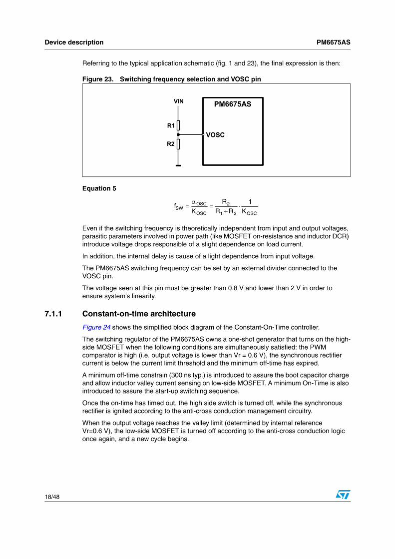
Referring to the typical application schematic (fig. 1 and 23), the final expression is then:
Figure 23. Switching frequency selection and VOSC pin
Equation 5
Even if the switching frequency is theoretically independent from input and output voltages, parasitic parameters involved in power path (like MOSFET on-resistance and inductor DCR) introduce voltage drops responsible of a slight dependence on load current.
In addition, the internal delay is cause of a light dependence from input voltage.
The PM6675AS switching frequency can be set by an external divider connected to the VOSC pin.
The voltage seen at this pin must be greater than 0.8 V and lower than 2 V in order to ensure system's linearity.
7.1.1 Constant-on-time architecture
Figure 24 shows the simplified block diagram of the Constant-On-Time controller.
The switching regulator of the PM6675AS owns a one-shot generator that turns on the high-side MOSFET when the following conditions are simultaneously satisfied: the PWM comparator is high (i.e. output voltage is lower than Vr = 0.6 V), the synchronous rectifier current is below the current limit threshold and the minimum off-time has expired.
A minimum off-time constrain (300 ns typ.) is introduced to assure the boot capacitor charge and allow inductor valley current sensing on low-side MOSFET. A minimum On-Time is also introduced to assure the start-up switching sequence.
Once the on-time has timed out, the high side switch is turned off, while the synchronous rectifier is ignited according to the anti-cross conduction management circuitry.
When the output voltage reaches the valley limit (determined by internal reference Vr=0.6 V), the low-side MOSFET is turned off according to the anti-cross conduction logic once again, and a new cycle begins.
PM6675AS
VOSC R1
R2
VIN
OSC21
2
OSC
OSCSW K
1RR
RK
f ⋅+
=α
=

PM6675AS Device description
19/48
Figure 24. Switching section simplified block diagram
7.1.2 Output ripple compensation and loop stability
The loop is closed connecting the center tap of the output divider (internally, when the fixed output voltage is chosen, or externally, using the VSEL pin in the adjustable output voltage mode). The feedback node is the negative input of the error comparator, while the positive input is internally connected to the reference voltage (Vr = 0.6 V). When the feedback voltage becomes lower than the reference voltage, the PWM comparator goes high and sets the control logic, turning on the high-side MOSFET. After the On-Time (calculated as previously described) the system releases the high-side MOSFET and turns-on the synchronous rectifier.
The voltage drop along ground and supply PCB paths, used to connect the output capacitor to the load, is a source of DC error. Further the system regulates the output voltage valley, not the average, as shown in Figure 22. Thus, the voltage ripple on the output capacitor is an additional source of DC error. To compensate this error, an integrative network is introduced in the control loop, by connecting the output voltage to the COMP pin through a capacitor (CINT) as shown in Figure 25.
+ -
HHSS LLeevveell sshhiifftteerr
LLSS
Q
QR
S
TToonn--mmiinn
Anti cross- conduction circuitry
TTooffff--mmiinn
Q
R
S
+ -
PPWWMM CCoommppaarraattoorr
PPoossiittiivvee CCuurrrreenntt LLiimmiitt ccoommppaarraattoorr
00..66VV
Q
QR
S
+_
MMiinn ffssww ccoouunntteerr ZZeerroo--ccrroossssiinngg CCoommppaarraattoorr
bbaannddggaapp 11..223366VV
PPHHAASSEE
PPGGNNDD
LLGGAATTEE
BBOOOOTT
CCSSNNSS
+
CCOOMMPP ggmm IInntteeggrraattoorr
VVSSNNSS
VVBBGG
VVBBGG PPUULLSSEE -- SSKKIIPP
VVSSEELL VSEL<4V
1-Shot generator
TToonn
VVSSNNSSVVOOSSCC
00..66VV
110000uuAA
500mV 2.5V
2.5V+-
-
-
+
+
HHGGAATTEE
VVRREEFF SSGGNNDD
VVOOSSCC
VVOOSSCC
VVCCCC
Device description PM6675AS
20/48
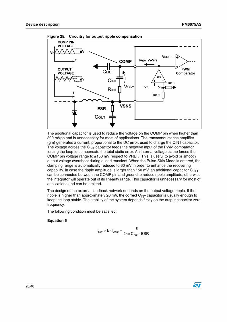
Figure 25. Circuitry for output ripple compensation
The additional capacitor is used to reduce the voltage on the COMP pin when higher than 300 mVpp and is unnecessary for most of applications. The transconductance amplifier (gm) generates a current, proportional to the DC error, used to charge the CINT capacitor. The voltage across the CINT capacitor feeds the negative input of the PWM comparator, forcing the loop to compensate the total static error. An internal voltage clamp forces the COMP pin voltage range to ±150 mV respect to VREF. This is useful to avoid or smooth output voltage overshoot during a load transient. When the Pulse-Skip Mode is entered, the clamping range is automatically reduced to 60 mV in order to enhance the recovering capability. In case the ripple amplitude is larger than 150 mV, an additional capacitor CFILT can be connected between the COMP pin and ground to reduce ripple amplitude, otherwise the integrator will operate out of its linearity range. This capacitor is unnecessary for most of applications and can be omitted.
The design of the external feedback network depends on the output voltage ripple. If the ripple is higher than approximately 20 mV, the correct CINT capacitor is usually enough to keep the loop stable. The stability of the system depends firstly on the output capacitor zero frequency.
The following condition must be satisfied:
Equation 6
+
-
VVRREEFF CCOOMMPP
ggmm
VVSSNNSS
RRFFbb11
RRFFbb22
VVrr+
PPWWMM CCoommppaarraattoorr
CCIINNTT
RRIINNTT
CCFFIILLTT
t Vr
CCOOUUTT
COMP PIN VOLTAGE
OUTPUT VOLTAGE
I=gm(V1-Vr)
VV11
t ∆V
∆V
VVCCIINNTT
EESSRR
ESRC2k
fkfout
ZoutSW ××π=×>
PM6675AS Device description
21/48
where k is a fixed design parameter (k > 3). It determinates the minimum integrator capacitor value:
Equation 7
where gm = 50 µs is the integrator transconductance.
If the ripple on the COMP pin is greater than the integrator 150 mV, the auxiliary capacitor CFILT can be added. If q is the desired attenuation factor of the output ripple, CFILT is given by:
Equation 8
In order to reduce the noise on the COMP pin, it is possible to add a resistor RINT that, together with CINT and CFILT, realizes a low pass filter. The cutoff frequency fCUT must be greater (10 or more times) than the switching frequency:
Equation 9
If the ripple is very small (lower than approximately 20 mV), a different compensation network, called "Virtual-ESR" Network, is needed. This additional circuit generates a triangular ripple that is added to the output voltage ripple at the input of the integrator. The complete control scheme is shown in Figure 26.
VoutVr
fk
f2
gC
ZoutSW
mINT ⋅
⎟⎠
⎞⎜⎝
⎛ −⋅π>
q)q1(C
C INTFILT
−⋅=
FILTINT
FILTINTCUT
INT
CCCC
f2
1R
+⋅
⋅⋅π=
Device description PM6675AS
22/48
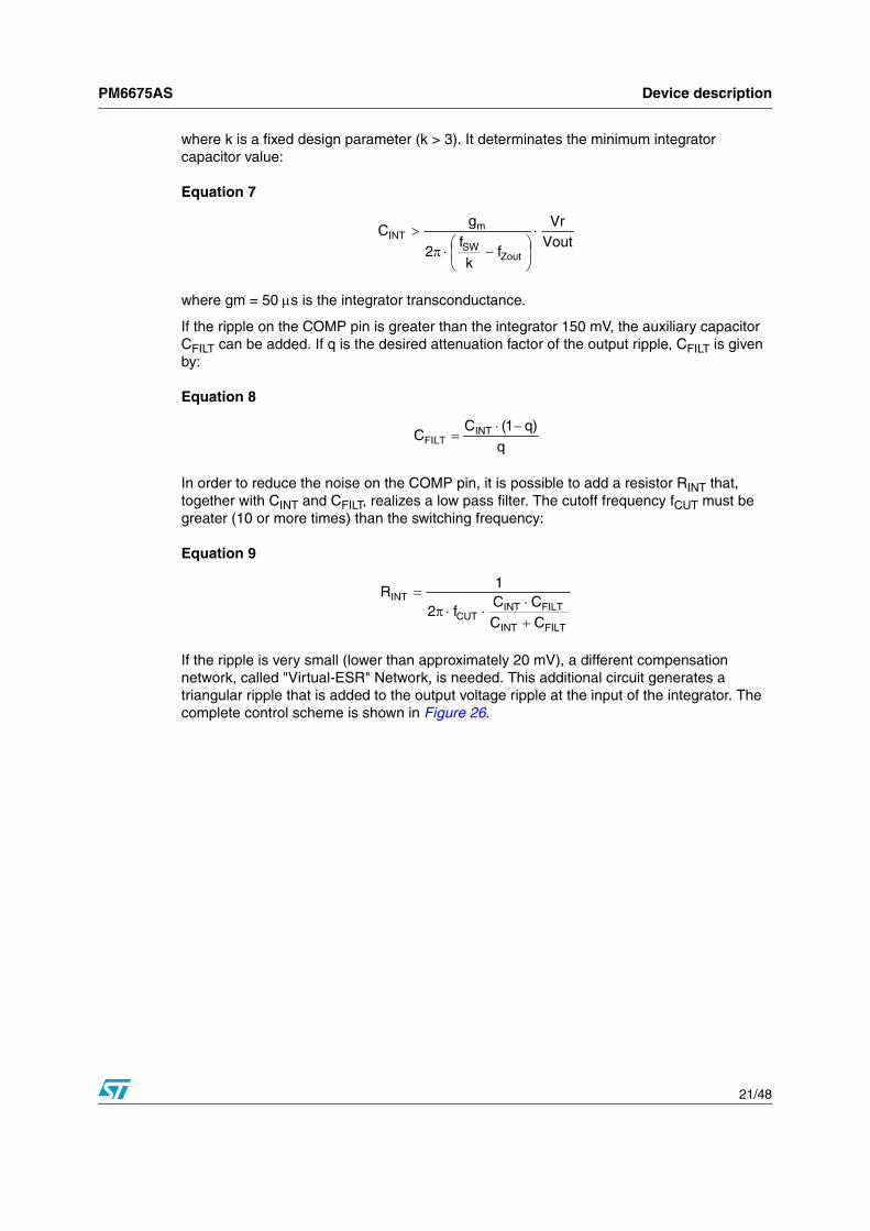
Figure 26. "Virtual-ESR" network
The ripple on the COMP pin is the sum of the output voltage ripple and the triangular ripple generated by the Virtual-ESR Network. In fact the Virtual-ESR Network behaves like a further equivalent series resistor RVESR.
A good trade-off is to design the network in order to achieve an RVESR given by:
Equation 10
where ∆IL is the inductor current ripple and VRIPPLE is the total ripple at the T node, chosen greater than approximately 20 mV.
The new closed-loop gain depends on CINT. In order to ensure stability it must be verified that:
Equation 11
where:
Equation 12
CCOOMMPP
VVSSNNSS
CCIINNTTRRIINNTTCCFFIILLTT
t
VREF
CCOOUUTT
COMP PIN VOLTAGE
OUTPUT VOLTAGE
CCRR
RR11
t
t
T
T NODE VOLTAGE
ΔV
ΔV2
EESSRR
ΔV1
+
-
VVRREEFF
ggmm
RRFFbb11
RRFFbb22
VVrr+
PPWWMM CCoommppaarraattoorr
I=gm(V1-Vr)
VV11
ESRI
VR
L
RIPPLEVESR −
∆=
VoutVr
f2g
CZ
mINT ⋅
⋅π>
TOToutZ RC2
1f
⋅⋅π=

PM6675AS Device description
23/48
and
Equation 13
Moreover, the CINT capacitor must meet the following condition:
Equation 14
where RTOT is the sum of the ESR of the output capacitor and the equivalent ESR given by the Virtual-ESR Network (RVESR). The k parameter must be greater than unity (k > 3) and determines the minimum integrator capacitor value CINT:
Equation 15
The capacitor of the Virtual-ESR Network, C, is chosen as follow
Equation 16
and R is calculated to provide the desired triangular ripple voltage:
Equation 17
Finally, the R1 resistor can be selected according to expression 18:
Equation 18
RTOT ESR RVERS+=
TOToutZSW RC2
kfkf
⋅⋅π=⋅>
VoutVr
fk
f2
gC
ZSW
mINT ⋅
⎟⎠
⎞⎜⎝
⎛−⋅π
>
INTC5C ⋅>
CRL
RVESR ⋅
=
Cf1
R
Cf1
R
1R
Z
Z
⋅⋅π−
⎟⎟⎠
⎞⎜⎜⎝
⎛⋅⋅π
⋅=

Device description PM6675AS
24/48
7.1.3 Pulse-skip and no-audible pulse-skip modes
High efficiency at light load conditions is achieved by PM6675AS entering the Pulse-Skip Mode (if enabled). At light load conditions the zero-crossing comparator truncates the low-side switch On-Time as soon as the inductor current becomes negative; in this way the comparator determines the On-Time duration instead of the output ripple (see Figure 27).
Figure 27. Inductor current and output voltage at light load with Pulse-Skip
As a consequence, the output capacitor is left floating and its discharge depends solely on the current drained from the load. When the output ripple on the pin COMP falls under the reference, a new shot is triggered and the next cycle begins. The Pulse-Skip mode is naturally obtained enabling the zero-crossing comparator and automatically takes part in the COT algorithm when the inductor current is about half the ripple current amount, i.e. migrating from continuous conduction mode (C.C.M.) to discontinuous conduction mode (D.C.M.).
The output current threshold related to the transition between PWM Mode and Pulse-Skip Mode can be approximately calculated as:
Equation 19
At higher loads, the inductor current never crosses the zero and the device works in pure PWM mode with a switching frequency around the nominal value.
A physiological consequence of Pulse-Skip Mode is a more noisy and asynchronous (than normal conditions) output, mainly due to very low load. If the Pulse-Skip is not compatible with the application, the PM6675AS allows the user to choose also between forced-PWM and No-Audible Pulse-Skip alternative modes (see Chapter 7.1.4 for details).
Output voltage
Inductor current
Vreg
TON TOFF
ONOUTIN
LOAD TL2
VV)Skip2PWM(I ⋅
⋅−
=

PM6675AS Device description
25/48
No-audible pulse-skip mode
Some audio-noise sensitive applications cannot accept the switching frequency to enter the audible range as is possible in Pulse-Skip mode with very light loads. For this reason, the PM6675AS implements an additional feature to maintain a minimum switching frequency of 33 kHz despite of a slight efficiency loss. At very light load conditions, if any switching cycle has taken place within 30 µs (typ.) since the last one (because of the output voltage is still higher than the reference), a No-audible pulse-skip cycle begins. The low-side MOSFET is turned on and the output is driven to fall until the reference has been crossed. Then, the high-side switch is turned on for a Ton period and, once it has expired, the synchronous rectifier is enabled until the inductor current reaches the zero-crossing threshold (see Figure 28).
Figure 28. Inductor current and output voltage at light load with non-audible pulse-skip
For frequencies higher than 33 kHz (due to heavier loads) the device works in the same way as in Pulse-Skip mode. It is important to notice that in both pulse-skip and no-audible Pulse-Skip modes the switching frequency changes not only with the load but also with the input voltage.
Output voltage
Inductor current
Vreg
t
TMAX
TON TOFF TIDLE

Device description PM6675AS
26/48
7.1.4 Mode-of-operation selection
Figure 29. VSEL and NOSKIP multifunction pin configurations
The PM6675AS has been designed to satisfy the widest range of applications. The device is provided of some multilevel pins which allow the user to choose the appropriate configuration. The VSEL pin is used to firstly decide between fixed preset or adjustable (user defined) output voltages.
When the VSEL pin is connected to +5 V, the PM6675AS set the switching section output voltage to 1.5 V without the need of an external divider.
Applications requiring different output voltages can be managed by PM6675AS simply setting the adjustable mode. If the VSEL pin voltage is higher than 4 V, the fixed output mode is selected. Connecting an external divider to the VSEL pin, it is used as negative input of the error amplifier and the output voltage is given by expression (20).
Equation 20
The output voltage can be set in the range from 0.6 V to 3.3 V.
The NOSKIP is the power saving algorithm selector: if tied to +5 V, the forced-PWM (fixed frequency) control is performed. If grounded or connected to VREF pin (1.237 V reference voltage), the Pulse-Skip or Non-Audible Pulse-Skip Modes are respectively selected.
Table 8. Mode-of-operation settings summary
VSEL NOSKIP VOUT Operating mode
VVSEL > 4.3V
VNOSKI P > 4.2 V
1.5 V
Forced-PWM
1V < VNOSKIP < 3.5 V Non-Audible Pulse-skip
< 0.5 V Pulse-Skip
VVSEL < 3.7V
VNOSKIP > 4.2 V
ADJ
Forced-PWM
1 V < VNOSKIP < 3.5 V Non-Audible Pulse-skip
VNOSKIP < 0.5 V Pulse-Skip
PM6675AS
NOSKIP
VSELR9 R8
VOUT
+5V
VREF
8R9R8R
6.0VOUTADJ+
⋅=

PM6675AS Device description
27/48
7.1.5 Current sensing and current limit
The PM6675AS switching controller employes a valley current sensing algorithm to properly handle the current limit protection and the inductor current zero-crossing information. The current is sensed during the conduction time of the low-side MOSFET. The current sensing element is the low-side MOSFET on-resistance. The sensing scheme is visible in Figure 30.
Figure 30. Current sensing scheme
An internal 100 µA current source is connected to CSNS pin that is also the non-inverting input of the positive current limit comparator. When the voltage drop developed across the sensing parameter equals the voltage drop across the programming resistor RILIM, the controller skips subsequent cycles until the overcurrent is detected or the output UV protection latches off the device (see par. Chapter 7.1.4 UV and OV Protections).
Referring to Figure 30, the RDSon sensing technique is tailored to all low cost, high efficiency applications.
It must be taken into account that the current limit circuit actually regulates the inductor valley current. This means that RILIM must be calculated to set a limit threshold given by the maximum DC output current plus half of the inductor ripple current:
Equation 21
where RSENSE is the sensing device (RDSon).
The PM6675AS provides also a fixed negative current limit to prevent excessive reverse inductor current when the switching section sinks current from the load in forced-PWM (3rd quadrant working conditions). This negative current limit threshold is measured between PHASE and PGND pins, comparing the drop magnitude on PHASE pin with an internal 110mV fixed voltage.
RILIM
HGATE
PHASE
CSNS
LGATE
PGND
SENSE
ILIMCL R
RA100I ⋅µ=

Device description PM6675AS
28/48
7.1.6 POR, UVLO and soft-start
The PM6675AS automatically performs an internal startup sequence during the rising phase of the analog supply of the device (AVCC). The switching controller remains in a stand-by state until AVCC crosses the upper UVLO threshold (4.25 V typ.), keeping active the internal discharge MOSFETs (only if AVCC > 1 V).
The soft-start allows a gradual increase of the internal current limit threshold during startup reducing the input/output surge currents. At the beginning of start-up, the PM6675AS current limit is set to 25 % of nominal value and the under voltage protection is disabled. Then, the current limit threshold is sequentially brought to 100 % in four steps of approximately 750 µs (figure 13).
Figure 31. Soft-start waveforms
After a fixed 3 ms total time, the soft-start finishes and UVP is released: if the output voltage doesn't reach the under voltage lower threshold within soft-start duration, the UVP condition is detected; the device performs a soft end and latches off. Depending on the load conditions, the inductor current may or may not reach the nominal value of the current limit (Figure 32 on page 29 shows two examples).
SWEN
Current limit threshold
Switching output
Time

PM6675AS Device description
29/48
7.1.7 Switching section power-good signal
The SPG pin is an open drain output used to monitor output voltage through VSNS (in fixed output voltage mode) or VSEL (in adjustable output voltage mode) pins and is enabled after the soft-start timer has expired. The SPG signal is held low if the output voltage drops 10 % below or rises 10 % above the nominal regulated value. The SPG output can sink current up to 4 mA.
7.1.8 Switching section output discharge
Active soft-end of the output occurs when the SWEN (SWitching ENable) is forced low. When the switching section is turned off, an internal 25 Ω resistor discharges the output through the VSNS pin.
Figure 33. Switching section soft-end
Figure 32. Soft-start at heavy load (a) and short-circuit (b) condition, pulse-skip enabled
(a) (b)
SWEN
VOUT
Resistive Discharge
Device description PM6675AS
30/48
7.1.9 Gate drivers
The integrated high-current gate drivers allow using different power MOSFETs. The high-side driver employes a bootstrap circuit which is supplied by the +5 V rail. The BOOT and PHASE pins work respectively as supply and return path for the high-side driver, while the low-side driver is directly feed through VCC and PGND pins.
An important feature of the PM6675AS gate drivers is the Adaptive Anti-Cross-Conduction circuitry, which prevents high-side and low-side MOSFETs from being turned on at the same time. When the high-side MOSFET is turned off, the voltage at the PHASE node begins to fall. The low-side MOSFET is turned on only when the voltage at the PHASE node reaches an internal threshold (2.5 V typ.). Similarly, when the low-side MOSFET is turned off, the high-side one remains off until the LGATE pin voltage is above 1 V.
The power dissipation of the drivers is a function of the total gate charge of the external power MOSFETs and the switching frequency, as shown in the following equation:
Equation 22
The low-side driver has been designed to have a low-resistance pull-down transistor (0.6 Ω typ.) in order to prevent undesired ignition of the low-side MOSFET due to the Miller effect.
7.1.10 Reference voltage and bandgap
The 1.237 V internal bandgap reference has a granted accuracy of ±1 % over the -25 °C to 85 °C temperature range. The VREF pin is a buffered replica of the bandgap voltage. It can supply up to ±100 µA and is suitable to set the intermediate level of NOSKIP multifunction pin. A 100 nF (min.) bypass capacitor toward SGND is required to enhance noise rejection. If VREF falls below 0.8 V (typ.), the system detects a fault condition and all the circuitry is turned off.
An internal divider derives a 0.6 V±1 % voltage (Vr) from the bandgap. This voltage is used as reference for both the switching and the linear sections. The Over-Voltage Protection, the Under-Voltage Protection and the power-good signals are also referred to Vr.
7.1.11 Switching section OV and UV protections
When the switching output voltage is about 115 % of its nominal value, a latched Over-Voltage Protection (OVP) occurs. In this case the synchronous rectifier immediately turns on while the high-side MOSFET turns off. The output capacitor is rapidly discharged and the load is preserved from being damaged. The OVP is also active during the soft-start. Once an OVP has taken part, a toggle on SWEN pin or a power-on-reset is necessary to exit from the latched state.
When the switching output voltage is below 70 % of its nominal value, a latched Under-Voltage Protection occurs. This event causes the switching section to be immediately disabled and both switches to be opened. The controller performs a soft-end and the output is eventually kept to ground, turning the low side MOSFET on when the voltage is lower than 400 mV.
SWgDRVD fQV)driver(P ⋅⋅=

PM6675AS Device description
31/48
The Under-Voltage Protection circuit is enabled only at the end of the soft-start. Once an UVP has taken part, a toggle on SWEN pin or a Power-On-Reset is necessary to clear the fault state and restart the section.
7.1.12 Device thermal protection
The internal control circuitry of the PM6675AS self-monitors the junction temperature and turns all outputs off when the 150 °C limit has been overran. This event causes the switching section to be immediately disabled and both switches to be opened. The controller performs a soft-end and both the outputs are eventually kept to ground, then the low side MOSFET is turned on when the voltage of the switching section is lower than 400 mV.
The thermal fault is a latched protection and normal operating condition is restored by a Power-On Reset or toggling SWEN and LEN pins at the same time.
7.2 LDO linear regulator sectionThe independent Low-Drop-Out (LDO) linear regulator has been designed to sink and source up to 2 A peak current and 1 A continuously. The LDO output voltage can be adjusted in the range 0.6 V to 3.3 V simply connecting a resistor divider as shown in Figure 34 on page 32.
Equation 23
Table 9. Switching section OV, UV and OT faults management
Fault Conditions Action
Over voltage VOUT > 115 % of the
nominal valueLGATE pin is forced high and the device latches off.
Exit by a Power-On Reset or toggling SWEN
Under voltage VOUT < 70 % of the nominal
value
LGATE pin is forced high after the soft-end, then the device latches off. Exit by a Power-On Reset or toggling SWEN.
Junction over temperature
TJ > +150 °CLGATE pin is forced high after the soft-end, then the device latches off. Exit by a Power-On Reset or toggling SWEN and LEN after temperature drop.
20R20R19R
6.0VLDOADJ+
⋅=

Device description PM6675AS
32/48
Figure 34. LDO output voltage selection
A compensation capacitor Cc must be added to adjust the dynamic response of the loop. The value of Cc is calculated according to the desired bandwidth of the LDO regulator and depends on the value of the feedback resistors. In most of applications the pole due to the compensation capacitor is placed at 100-200 kHz (equation 24).
Equation 24
The LIN input can be connected to the switching section output for compact solutions or to a lower supply, if available in the system, in order to reduce the power dissipation of the LDO.
A minimum output capacitance of 20 µF (2x10 µF MLCC capacitors) is enough to assure stability and fast load transient response.
7.2.1 LDO section current limit
The LDO regulator can handle up to ±2 Apk, depending on the LDO input voltage and the LILIM pin setting. The output current is limited to ±1 A or ±2 A if the LILIM pin is connected to SGND or AVCC respectively (Figure 35).
Figure 35. LDO current limit setting
The maximum current that the LDO can source depends also on the input and output voltages. Due to the high side MOSFET of the output stage, the LDO cannot source the limit current at high output voltages. Figure 36 shows the maximum current that the LDO can source as function of the input and output voltages. For output voltages higher than 2 V, the maximum output current is limited as reported.
PM6675AS
LFB
LOUT
R19
R20
VLOUT
LGND
CcCOUT
kHz200C)20R19R(2
1f
Cp =
⋅⊕π=
PM6675AS
LILIM
+5V
±2A CL
±1A CL

PM6675AS Device description
33/48
Figure 36. LDO current limit setting
7.2.2 LDO section soft-start
The LDO section soft-start is performed by clamping the current limit. During startup, the LDO current limit voltage is set to 1 A and the output voltage increases linearly. When the output voltage rises above 90 % of the nominal value, the current limit is released to 2 A according to the LILIM pin setting.
7.2.3 LDO section power-good signal
The LPG pin is an open drain output used to monitor the LDO output voltage through LFB pin. The LPG signal is held low if the output voltage drops 10 % below or rises 10 % above the nominal regulated value. The LPG output can sink current up to 4 mA.
7.2.4 LDO section output discharge
Active soft-end of the LDO output occurs when the LEN (Linear ENable) is forced low. When the LDO section is turned off, an internal 25 Ω resistor, directly connected to the LOUT pin, discharges the output.
Figure 37. LDO section soft-end
0.0
0.2
0.4
0.6
0.8
1.0
1.2
1.4
1.6
1.8
2.0
2.2
0.0 0.5 1.0 1.5 2.0 2.5 3.0 3.5 4.0 4.5 5.0
VLIN [V]
ILO
UT
[A]
VOUT=1.05V
VOUT=1.2V
VOUT=1.5VVOUT=1.8V
VOUT=2.0V
VOUT=2.2V
VOUT=2.5VVOUT=3.3V
LEN
VLDO
Resistive Discharge
Application information PM6675AS
34/48
8 Application information
The purpose of this chapter is to show the design procedure of the switching section.
The design starts from three main specifications:
The input voltage range, provided by the battery or the AC adapter. The two extreme values (VINmax and VINmin) are important for the design.
The maximum load current, indicated with ILOAD,MAX .
The maximum allowed output voltage ripple VRIPPLE,MAX.
It’s also possible that specific designs should involve other specifications.
The following paragraphs will guide the user into a step-by-step design.
8.1 External components selectionThe PM6675AS employes a pseudo-fixed frequency, Constant On-Time (COT) controller as the core of the switching section. The switching frequency can be set by connecting an external divider to the VOSC pin. The voltage seen at this pin must be greater than 0.8 V and lower than 2 V in order to take advantage of the internal block linearity.
Nearly constant switching frequency is achieved by the system loop in steady-state operating conditions by varying the On-Time duration, avoiding thus the need for a clock generator. The On-Time one shot duration is directly proportional to the output voltage, sensed at VSNS pin, and inversely proportional to the input voltage, sensed at the VOSC pin, as follows:
Equation 25
where KOSC is a constant value (130 ns typ.) and τ is the internal propagation delay(40 ns typ.).
The duty-cycle of the buck converter is, in steady-state conditions, given by
Equation 26
The switching frequency is thus calculated as
Equation 27
τ+=OSC
SNSOSCON V
VKT
IN
OUT
V
VD =
OSCOUT
OSC
OSC
SNSOSC
IN
OUT
ONSW K
1
V
VK
V
V
TD
f ⋅αα
=⋅
==
PM6675AS Application information
35/48
Equation 28 a
Equation 28 b
Referring to the typical application schematic (figs. 1 and 23), the final expression is then:
Equation 29
Even if the switching frequency is theoretically independent from battery and output voltages, parasitic parameters involved in power path (like MOSFETs on-resistance and inductor DCR) introduce voltage drops responsible of a slight dependence on load current.
In addition, the internal delay is cause of a light dependence from input voltage.
8.1.1 Inductor selection
Once the switching frequency has been defined, the inductance value depends on the desired inductor ripple current. Low inductance value means great ripple current that brings to poor efficiency and great output noise. On the other hand a great current ripple is desirable for fast transient response when a load step is applied.
Otherwise, great inductance brings to good efficiency but the transient response is critical, especially if VINmin - Vout is little. Moreover a minimum output ripple voltage is necessary to assure system stability and jitter-free operations (see Output capacitor selection paragraph). The product of the output capacitor ESR multiplied by the inductor ripple current must be taken into consideration. A good trade-off between the transient response time, the efficiency, the cost and the size is to choose the inductance value in order to maintain the inductor ripple current between 20 % and 50 % (usually 40 %) of the maximum output current.
The maximum inductor ripple current, ∆ILMAX, occurs at the maximum input voltage.
Table 10. Typical values for switching frequency selection
R1 (kΩ) R2 (kΩ) Approx switching frequency (kHz)
330 11 250
330 13 300
330 15 350
330 18 400
330 20 450
330 22 500
IN
OSCOSC V
V=α
OUT
SNSOUT V
V=α
OSC21
2
OSC
OSCSW K
1RR
R
Kf ⋅
+=
α=

Application information PM6675AS
36/48
With these considerations, the inductance value can be calculated with the following expression:
Equation 30
where fSW is the switching frequency, VIN is the input voltage, VOUT is the output voltage and is the inductor current ripple.
Once the inductor value is determined, the inductor current ripple is then recalculated:
Equation 31
The next step is the calculation of the maximum r.m.s. inductor current:
Equation 32
The inductor must have an r.m.s. current greater than IL,RMS in order to assure thermal stability.
Then the calculation of the maximum inductor peak current follows:
Equation 33
ILPEAK is important in inductor selection in term of its saturation current. The saturation current of the inductor should be greater than ILPEAK not only in case of hard saturation core inductors. Using soft-ferrite cores it is possible (but not advisable) to push the inductor working near its saturation current.
In Table 11 some inductors suitable for typical working conditions are listed.
Table 11. Evaluated inductors (@ fsw = 400 kHz)
Manufacturer SeriesInductance
(µH)+40°C rms current (A)
-30% saturation current (A)
COILCRAFT MLC1538-102 1 13.4 21.0
COILCRAFT MVR1261C-112 1.1 20 20
WURTH 7443552100 1 16 20
COILTRONICS HC8-1R2 1.2 16.0 25.4
IN
OUT
L
OUTIN
V
V
Ifsw
VVL ⋅
∆⋅−
=
MAX,IN
OUTOUTMAX,INMAX,L V
V
Lfsw
VVI ⋅
⋅
−=∆
12
)I()I(I
2MAX,L2
MAX,LOADRMS,L∆
+=
2
III MAX,L
MAX,LOADPEAK,L∆
+=

PM6675AS Application information
37/48
In Pulse-Skip Mode, low inductance values produce a better efficiency versus load curve, while higher values result in higher full-load efficiency because of the smaller current ripple.
8.1.2 Input capacitor selection
In a buck topology converter the current that flows through the input capacitor is pulsed and with zero average value. The RMS input current can be calculated as follows:
Equation 34
Neglecting the second term, the equation 34 is reduced to:
Equation 35
The losses due to the input capacitor are thus maximized when the duty-cycle is 0.5:
Equation 36
The input capacitor should be selected with a RMS rated current higher than ICinRMS. Tantalum capacitors are good in term of low ESR and small size, but they occasionally can burn out if subjected to very high current during operation. Multi-Layers-Ceramic-Capacitors (MLCC) have usually a higher RMS current rating with smaller size and they remain the best choice. The drawback is their quite high cost.
It must be taken in account that MLCC capacitance decreases when the operating voltage is near the rated voltage. In table 12 some MLCC suitable for most of applications are listed.
Table 12. Evaluated MLCC for input filtering
Manufacturer SeriesCapacitance
(µF)Rated voltage
(V)Maximum Irms @100 kHz (A)
TAIYO YUDEN UMK325BJ106KM-T 10 50 2
TAIYO YUDEN GMK316F106ZL-T 10 35 2.2
TAIYO YUDEN GMK325F106ZH-T 10 35 2.2
TAIYO YUDEN GMK325BJ106KN 10 35 2.5
TDK C3225X5R1E106M 10 25
2L
2LOADRMSCin )I(D
121
)D1(DII ∆⋅+−⋅⋅=
)D1(DII LOADRMSCin −⋅=
2LOADCin
2CinRMSCinloss (max))I5.0(ESR(max)IESRP ⋅⋅=⋅=

Application information PM6675AS
38/48
8.1.3 Output capacitor selection
Using tantalum or electrolytic capacitors, the selection is made referring to ESR and voltage rating rather than by a specific capacitance value.
The output capacitor has to satisfy the output voltage ripple requirements. At a given switching frequency, small inductor values are useful to reduce the size of the choke but increase the inductor current ripple. Thus, to reduce the output voltage ripple a low ESR capacitor is required.
To reduce jitter noise between different switching regulators in the system, it is preferable to work with an output voltage ripple greater than 25 mV.
As far as it concerns the load transient requirements, the Equivalent Series Resistance (ESR) of the output capacitor must satisfy this relationship:
Equation 37
where VRIPPLE is the maximum tolerable ripple voltage.
In addition, the ESR must be enough high to meet stability requirements. The output capacitor zero must be lower than the switching frequency:
Equation 38
If ceramic capacitors are used, the output voltage ripple due to inductor current ripple is negligible; then the inductance could be smaller, reducing the size of the choke. In this case it is important that the output capacitor can adsorb the inductor energy without generating an over-voltage condition when the system changes from a full load to a no load condition.
The minimum output capacitance can be chosen by the following equation:
Equation 39
where Vf is the output capacitor voltage after the load transient and Vi is the output capacitor voltage before the load transient.
MAX,L
MAX,RIPPLE
I
VESR
∆≤
outZSW CESR2
1ff
⋅⋅π=>
22
2MAX,LOAD
min,OUTViVf
ILC
−
⋅=

PM6675AS Application information
39/48
In Table 13 some tested polymer capacitors are listed.
8.1.4 MOSFETs selection
In SMPS converters, power management efficiency is a high level requirement, so the power dissipation on the power switches becomes an important factor in switches selection. Losses of high-side and low-side MOSFETs depend on their working condition.
Considering the high-side MOSFET, the power dissipation is calculated as:
Equation 40
Maximum conduction losses are approximately given by:
Equation 41
where RDSon is the MOSFET drain-source on-resistance.
Switching losses are approximately given by:
Equation 42
where tON and tOFF are the turn-on and turn-off times of the MOSFET and depend on the gate-driver current capability and the gate charge Qgate. A greater efficiency is achieved with low RDSon. Unfortunately low RDSon MOSFETs have a great gate charge.
As general rule, the RDSon . Qgate product should be minimized to find out the suitable
MOSFET.
Logic-level MOSFETs are recommended, as long as low-side and high-side gate drivers are powered by VVCC = +5 V. The breakdown voltage of the MOSFETs (VBRDSS) must be greater than the maximum input voltage VINmax.
Below some tested high-side MOSFETs are listed.
Table 13. Evaluated output capacitors
Manufacturer SeriesCapacitance
(µF)Rated voltage
(V)ESR max
@100kHz (mΩ)
SANYO 4TPE220MF 220 4 V 15 to 25
4TPE150MI 150 4 V 18
4TPC220M 220 4 V 40
HITACHI TNCB OE227MTRYF 220 2.5 V 25
switchingconductionDHighSide PPP +=
2MAX,LOAD
min.IN
OUTDSonconduction I
V
VRP ⋅⋅=
2
ft)2
I(max)I(V
2
ft)2
I(max)I(V
Pswoff
LLOADINswon
LLOADIN
switching
⋅⋅∆
+⋅+
⋅⋅∆
−⋅=

Application information PM6675AS
40/48
In buck converters the power dissipation of the synchronous MOSFET is mainly due to conduction losses:
Equation 43
Maximum conduction losses occur at the maximum input voltage:
Equation 44
The synchronous rectifier should have the lowest RDSon as possible. When the high-side MOSFET turns on, high dV/dt of the phase node can bring up even the low-side gate through its gate-drain capacitance CRES, causing cross-conduction problem. Once again, the choice of the low-side MOSFET is a trade-off between on resistance and gate charge; a good selection should minimizes the ratio CRSS / CGS where CGS = CISS - CRSS.
Below some tested low-side MOSFETs are listed.
Dual N-MOS can be used in applications with low output current.
Figure 16 shows some suitable dual MOSFETs for applications requiring about 3 A.
Table 14. Evaluated high-side MOSFETs
Manufacturer Type RDSon (mΩ) Gate charge (Nc) Rated reverse voltage (V)
ST STS12NH3LL 10.5 12 30
ST STS7NF60L 17 25 60
IR IRF7811 9 18 30
Table 15. Evaluated low-side MOSFETs
Manufacturer Type RDSon (mΩ)Rated reverse voltage
(V)
ST STS12NH3LL 13.5 0.069 30
ST STS25NH3LL 40 0.011 30
IR IRF7811 24 0.054 30
Table 16. Suitable dual MOSFETs
Manufacturer Type RDSon (mΩ) Gate charge (nC)Rated reverse
voltage (V)
ST STS8DNH3LL 25 10 30
IR IRF7313 46 33 30
conductionDLowSide PP ≅
2MAX,LOAD
MAX,IN
OUTDSonconduction I
V
V1RP ⋅⎟
⎟⎠
⎞⎜⎜⎝
⎛−⋅=
GS
GD
C
C
PM6675AS Application information
41/48
8.1.5 Diode selection
A rectifier across the synchronous switch is recommended. The rectifier works as a voltage clamp across the synchronous rectifier and reduces the negative inductor swing during the dead time between turning the high-side MOSFET off and the synchronous rectifier on. Moreover it increases the efficiency of the system.
The reverse voltage should be greater than the maximum input voltage VINmax and a minimum recovery reverse charge is preferable. Table 17 shows some evaluated diodes.
8.1.6 VOUT current limit setting
The valley current limit is set by RCSNS and must be chosen to support the maximum load current. The valley of the inductor current ILvalley is:
Equation 45
The output current limit depends on the current ripple as shown in Figure 38:
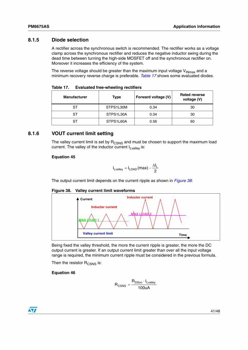
Figure 38. Valley current limit waveforms
Being fixed the valley threshold, the more the current ripple is greater, the more the DC output current is greater. If an output current limit greater than over all the input voltage range is required, the minimum current ripple must be considered in the previous formula.
Then the resistor RCSNS is:
Equation 46
Table 17. Evaluated free-wheeling rectifiers
Manufacturer Type Forward voltage (V)Rated reverse
voltage (V)
ST STPS1L30M 0.34 30
ST STPS1L30A 0.34 30
ST STPS1L60A 0.56 60
2I
(max)II LLOADLvalley
∆−=
Inductor current
Valley current limit
MAX LOAD 1
MAX LOAD 2
Current
Time
Inductor current
uA100
IRR
LvalleyDSonCSNS
⋅=

Application information PM6675AS
42/48
where RDSon is the drain-source on-resistance low-side switch. Consider the temperature effect and the worst case value in RDSon calculation (typically +0.4 %/°C).
The accuracy of the valley current also depends on the offset of the internal comparator(±6 mV).
The negative valley-current limit (if the device works in forced-PWM mode) is given by:
Equation 47
8.1.7 All ceramic capacitors application
Design of external feedback network depends on the output voltage ripple across the output capacitors ESR. If the ripple is great enough (at least 20 mV), the compensation network simply consist of a CINT capacitor.
Figure 39. Integrative compensation
The stability of the system depends firstly on the output capacitor zero frequency. It must be verified that:
Equation 48
DSonNEG R
mV110I =
CFILT CINTRINT
gm
+
- Vr=0.6
VSNS
Ton One-shot generator
VREF
PWM Comparator
+
-
COMP
VOUT
Integrator
outoutZoutSW CR2
kfkf
⋅π=⋅>

PM6675AS Application information
43/48
where k is a free design parameter greater than unity (k > 3) . It determinates the minimum integrator capacitor value CINT:
Equation 49
If the ripple on pin COMP is greater than the integrator output dynamic (150 mV), an additional capacitor Cfilt could be added in order to reduce its amplitude. If q is the desired attenuation factor of the output ripple, select:
Equation 50
In order to reduce noise on pin COMP, it’s possible to introduce a resistor RINT that, together with CINT and Cfilt, realizes a low pass filter. The cutoff frequency must be much greater (10 or more times) than the switching frequency of the section:
Equation 51
For most of applications both RINT and Cfilt are unnecessary.
If the ripple is very small (e.g. such as with ceramic capacitors), a further compensation network, called “Virtual ESR” network, is needed. This additional part generates a triangular ripple that substitutes the ESR output voltage ripple. The complete compensation scheme is represented in Figure 40.
Figure 40. Virtual ESR network
VoVref
fk
f2
gC
ZoutSW
mINT ⋅
⎟⎟⎠
⎞⎜⎜⎝
⎛−⋅π
>
q
)q1(CC INT
filt−⋅
=
FILTINT
FILTINTCUT
INT
CCCC
f2
1R
+⋅
⋅π=
VREF CFILT
CINT
RINT PWM Comparator
gm +
-
+
- 0.6V
VOUT
Ton Generation
Block
C
R R1
L
Integrator

Application information PM6675AS
44/48
Select C as shown:
Equation 52
Then calculate R in order to have enough ripple voltage on the integrator input:
Equation 53
Where RVERS is the new virtual output capacitor ESR. A good trade-off is to consider an equivalent ESR of 30-50 mΩ, even though the choice depends on inductor current ripple.
Then choose R1 as follows:
Equation 54
INTC5C ⋅>
CRL
RVESR ⋅
=
Z
Z
fC1
R
fC1
R
1R
π−
⎟⎟⎠
⎞⎜⎜⎝
⎛π
⋅
=

PM6675AS Package mechanical data
45/48
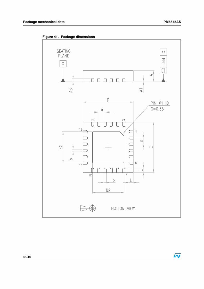
9 Package mechanical data
In order to meet environmental requirements, ST offers these devices in ECOPACK® packages. These packages have a Lead-free second level interconnect. The category of second Level Interconnect is marked on the package and on the inner box label, in compliance with JEDEC Standard JESD97. The maximum ratings related to soldering conditions are also marked on the inner box label. ECOPACK is an ST trademark. ECOPACK specifications are available at: www.st.com.
Table 18. VFQFPN-24 4mm x 4mm mechanical data
Dim. mm.
Min Typ Max
A 0.80 0.90 1.00
A1 0.0 0.05
A2 0.65 0.80
D 4.00
D1 3.75
E 4.00
E1 3.75
θ 12°
P 0.24 0.42 0.60
e 0.50
N 24.00
Nd 6.00
Ne 6.00
L 0.30 0.40 0.50
b 0.18 0.30
D2 1.95 2.10 2.25
E2 1.95 2.10 2.25
Package mechanical data PM6675AS
46/48
Figure 41. Package dimensions

PM6675AS Revision history
47/48
10 Revision history
Table 19. Document revision history
Date Revision Changes
19-Feb-2008 1 Initial release.

PM6675AS
48/48
Please Read Carefully:
Information in this document is provided solely in connection with ST products. STMicroelectronics NV and its subsidiaries (“ST”) reserve theright to make changes, corrections, modifications or improvements, to this document, and the products and services described herein at anytime, without notice.
All ST products are sold pursuant to ST’s terms and conditions of sale.
Purchasers are solely responsible for the choice, selection and use of the ST products and services described herein, and ST assumes noliability whatsoever relating to the choice, selection or use of the ST products and services described herein.
No license, express or implied, by estoppel or otherwise, to any intellectual property rights is granted under this document. If any part of thisdocument refers to any third party products or services it shall not be deemed a license grant by ST for the use of such third party productsor services, or any intellectual property contained therein or considered as a warranty covering the use in any manner whatsoever of suchthird party products or services or any intellectual property contained therein.
UNLESS OTHERWISE SET FORTH IN ST’S TERMS AND CONDITIONS OF SALE ST DISCLAIMS ANY EXPRESS OR IMPLIEDWARRANTY WITH RESPECT TO THE USE AND/OR SALE OF ST PRODUCTS INCLUDING WITHOUT LIMITATION IMPLIEDWARRANTIES OF MERCHANTABILITY, FITNESS FOR A PARTICULAR PURPOSE (AND THEIR EQUIVALENTS UNDER THE LAWSOF ANY JURISDICTION), OR INFRINGEMENT OF ANY PATENT, COPYRIGHT OR OTHER INTELLECTUAL PROPERTY RIGHT.
UNLESS EXPRESSLY APPROVED IN WRITING BY AN AUTHORIZED ST REPRESENTATIVE, ST PRODUCTS ARE NOTRECOMMENDED, AUTHORIZED OR WARRANTED FOR USE IN MILITARY, AIR CRAFT, SPACE, LIFE SAVING, OR LIFE SUSTAININGAPPLICATIONS, NOR IN PRODUCTS OR SYSTEMS WHERE FAILURE OR MALFUNCTION MAY RESULT IN PERSONAL INJURY,DEATH, OR SEVERE PROPERTY OR ENVIRONMENTAL DAMAGE. ST PRODUCTS WHICH ARE NOT SPECIFIED AS "AUTOMOTIVEGRADE" MAY ONLY BE USED IN AUTOMOTIVE APPLICATIONS AT USER’S OWN RISK.
Resale of ST products with provisions different from the statements and/or technical features set forth in this document shall immediately voidany warranty granted by ST for the ST product or service described herein and shall not create or extend in any manner whatsoever, anyliability of ST.
ST and the ST logo are trademarks or registered trademarks of ST in various countries.
Information in this document supersedes and replaces all information previously supplied.
The ST logo is a registered trademark of STMicroelectronics. All other names are the property of their respective owners.
© 2008 STMicroelectronics - All rights reserved
STMicroelectronics group of companies
Australia - Belgium - Brazil - Canada - China - Czech Republic - Finland - France - Germany - Hong Kong - India - Israel - Italy - Japan - Malaysia - Malta - Morocco - Singapore - Spain - Sweden - Switzerland - United Kingdom - United States of America
www.st.com