high-frequency and low-power output stages based...
TRANSCRIPT

Hindawi Publishing CorporationISRN ElectronicsVolume 2013, Article ID 914058, 7 pageshttp://dx.doi.org/10.1155/2013/914058
Research ArticleHigh-Frequency and Low-Power Output Stages Based onFGMOS Flipped Voltage Follower
Maneesha Gupta, Urvashi Singh, and Richa Srivastava
Department of Electronics and Communication Engineering, Netaji Subhas Institute of Technology, Sector 3,Dwarka, New Delhi 110078, India
Correspondence should be addressed to Maneesha Gupta; [email protected]
Received 29 November 2012; Accepted 25 December 2012
Academic Editors: C. W. Chiou and J.-Y. Sim
Copyright © 2013 Maneesha Gupta et al. This is an open access article distributed under the Creative Commons AttributionLicense, which permits unrestricted use, distribution, and reproduction in any medium, provided the original work is properlycited.
Twonewhigh-performance output stages are proposed.These output stages are basically designed byusing a flipped voltage follower(FVF). The proposed low-power and low-voltage output stages have utilized the advantages of the FGMOS technology. They arecharacterized by low-power dissipation, reduced power supply requirement, and larger bandwidth. By using FGMOS-based FVF inplace of conventional FVF, the linearity of the output stages has been highly improved. The small-signal analysis of FGMOS-basedFVF is done to show the bandwidth enhancement of conventional FVF.The circuits are simulated to demonstrate the effectivenessusing SPICE, in TSMC 0.25-micron CMOS device models. The simulation results show that the power supply requirement of theproposed output stages is highly reduced and bandwidths are extremely higher than the conventional circuits.
1. Introduction
The challenge of designing of high performance low-voltageand low-power analog circuits is increasing due to the scalingdown of CMOS technology and the increasing demand forportable electronic equipments [1].The speed of conventionalanalog integrated circuits is degrading on reducing the supplyvoltage for a given technology. To fulfill these requirements,the researchers are focusing on the development of newintegrated circuits that have low voltage supply requirement,without any degradation in the performance.
One of the basic building blocks in analog signal pro-cessing circuits is voltage buffer, which is used to drive low-impedance loads (Figure 1(a)). The flipped voltage follower(FVF) [2] is a low-voltage operating buffer that can be used indifferent circuits in place of conventional voltage buffer veryefficiently. A FVF circuit is shown in Figure 1(b).
A FVF cell has found increasing applications in areaswhere a voltage buffer is required. These applications includeoperational amplifier, current mirror, output stages, andarithmetic circuits and act as a basic building block in variousanalog circuits [2–7]. The advantages of FVF include lowsupply voltage requirement, almost unity gain, and highcurrent-sinking capabilities [2].
Ramirez-Angulo et al. [3] have introduced an FVF whichis based on FGMOS level shifter stage, shown in Figure 2.Due to its high swing and low voltage operation, the FGMOS-based FVF can be preferred over conventional FVF in manyhigh-swing, low-power, and wideband analog integratedcircuits.
Applications for communication systems require lowpower, low voltage, and high frequency output stages. Thesupply voltage and the power dissipation of output stagecan be reduced by using floating gate technology. There areseveral attractive features of FGMOS such as it can incorpo-rate tuneable mechanisms and work below the operationallimits of supply voltage levels for a particular technology,without affecting the other characteristics of the system,and thus power dissipation is also lesser than the minimumpower required for a MOS circuit of the same technology [8–13].
Usually buffers require an extra circuitry to achieve largebandwidth, which often increases power consumption. Inthis work, the FVF with floating gate level shifter [3] is usedto replace the conventional FVF in different output stages,which have been investigated by Centurelli et al. in [14].We have achieved high bandwidth of output stages, without

2 ISRN Electronics
Ib
VDD
M1
Vout
Vin
VSS
(a)
M1
M2
𝑉in
𝑉out
𝐼𝑏
𝑉SS
𝑉DD
𝑅𝑏
(b)
Figure 1: (a) Voltage follower and (b) flipped voltage follower.
M1
M2
𝑉in
𝑉out
𝐼𝑏
𝑉SS
𝑉DD
𝑅𝑏
𝐶1
𝐶2
Figure 2: FVF using floating gate level shifter [3].
affecting the gain of the system, and moreover the powerconsumption is highly reduced.
This paper is organized as follows. Section 2 covers thelarge signal analysis and small signal analysis of conventionalFVF with a floating gate level shifter. Section 3 presents theproposed output stages based on FGMOS FVF. On the basisof simulation results, the performances of designed circuitsare compared in Section 4. Finally, the conclusion is given inSection 5.
2. FVF with Floating Gate Level Shifter
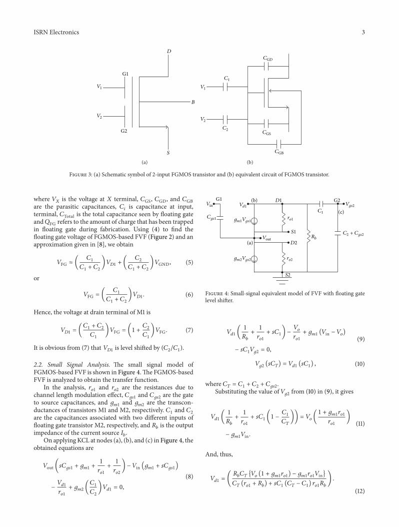
2.1. Large Signal Analysis. The symbolic representation oftwo-input floating gate transistor, whose threshold voltagecan be controlled by the values of capacitors, and its equiv-alent circuit are shown in Figures 3(a) and 3(b), respectively.
The input signal (𝑉1) and bias (𝑉
2) are applied at gate G1
and G2, respectively. The drain current (𝐼𝐷) of the FGMOS
operating in ohmic region is given by [8, 9]
𝐼𝐷= 𝛽[{(
𝐶1
𝐶Total𝑉1+
𝐶2
𝐶Total𝑉2+𝐶GD𝐶Total
𝑉DS)
− 𝑉𝑇} −
𝑉DS2]𝑉DS,
(1)
where𝛽 is the transconductance parameter,𝐶1and𝐶
2are the
capacitances associated with G1 and G2, 𝐶Total = 𝐶1+ 𝐶2+
𝐶GS + 𝐶GD + 𝐶GB is the total floating-gate (FG) capacitance,and 𝑉
𝑇stands for the threshold voltage. The above equation
can be simplified as
𝐼𝐷= 𝛽(
𝐶1
𝐶Total)[(𝑉
1− 𝑉𝑇,eff) 𝑉DS −
𝐶Total2𝐶1
𝑉2
DS] , (2)
where effective threshold voltage (𝑉𝑇,eff) is given by [8]
𝑉𝑇,eff = 𝑉𝑇 +
𝐶2
𝐶1
(𝑉𝑇− 𝑉2) . (3)
From (3), it is obvious that the reduction in 𝑉𝑇,eff can
be done by selecting 𝑉2> 𝑉𝑇and 𝐶
2> 𝐶1. Hence, 𝑉
𝑇,effis controllable and it depends on the values of 𝐶
1and 𝐶
2.
The proposed output stage circuits utilize this property of theFGMOS transistor.
The control gates (G1 and G2) develop a floating gatevoltage 𝑉FG as a weighted sum of inputs voltages 𝑉
𝑖, via a
capacitive voltage divider. 𝑉FG is given by [8]
𝑉FG = {
𝑁
∑
𝑖=1
(𝐶𝑖
𝐶Total)𝑉𝑖+ (
𝐶GS𝐶Total
)𝑉𝑆+ (
𝐶GD𝐶Total
)𝑉𝐷
+(𝐶GB𝐶Total
)𝑉𝐵+𝑄FG𝐶Total
} ,
(4)
ISRN Electronics 3
𝑉1
𝑉2
G1
G2
𝐷
𝐵
𝑆
(a)
𝑉1
𝑉2
𝐶1
𝐶2
𝐶GD
𝐶GS
𝐶GB
(b)
Figure 3: (a) Schematic symbol of 2-input FGMOS transistor and (b) equivalent circuit of FGMOS transistor.
where 𝑉𝑋is the voltage at 𝑋 terminal, 𝐶GS, 𝐶GD, and 𝐶GB
are the parasitic capacitances, 𝐶𝑖is capacitance at input,
terminal, 𝐶Total is the total capacitance seen by floating gateand𝑄FG refers to the amount of charge that has been trappedin floating gate during fabrication. Using (4) to find thefloating gate voltage of FGMOS-based FVF (Figure 2) and anapproximation given in [8], we obtain
𝑉FG ≈ (𝐶1
𝐶1+ 𝐶2
)𝑉𝐷1+ (
𝐶2
𝐶1+ 𝐶2
)𝑉GND, (5)
or
𝑉FG = (𝐶1
𝐶1+ 𝐶2
)𝑉𝐷1. (6)
Hence, the voltage at drain terminal of M1 is
𝑉𝐷1= (
𝐶1+ 𝐶2
𝐶1
)𝑉FG = (1 +𝐶2
𝐶1
)𝑉FG. (7)
It is obvious from (7) that 𝑉𝐷1
is level shifted by (𝐶2/𝐶1).
2.2. Small Signal Analysis. The small signal model ofFGMOS-based FVF is shown in Figure 4.The FGMOS-basedFVF is analyzed to obtain the transfer function.
In the analysis, 𝑟𝑜1
and 𝑟𝑜2
are the resistances due tochannel length modulation effect, 𝐶
𝑔𝑠1and 𝐶
𝑔𝑠2are the gate
to source capacitances, and 𝑔𝑚1
and 𝑔𝑚2
are the transcon-ductances of transistors M1 and M2, respectively. 𝐶
1and 𝐶
2
are the capacitances associated with two different inputs offloating gate transistor M2, respectively, and 𝑅
𝑏is the output
impedance of the current source 𝐼𝑏.
On applying KCL at nodes (a), (b), and (c) in Figure 4, theobtained equations are
𝑉out (𝑠𝐶𝑔𝑠1 + 𝑔𝑚1 +1
𝑟𝑜1
+1
𝑟𝑜2
) − 𝑉in (𝑔𝑚1 + 𝑠𝐶𝑔𝑠1)
−𝑉𝑑1
𝑟𝑜1
+ 𝑔𝑚2(𝐶1
𝐶2
)𝑉𝑑1= 0,
(8)
𝐶𝑔𝑠1
G1 (b)
(a)
(c)
𝑆2
𝑆1
𝐷2
𝑟𝑜1
𝑟𝑜2
𝐷1 G2
𝑅𝑏
𝐶1
𝐶2 + 𝐶𝑔𝑠2
𝑉in 𝑉𝑑1
𝑔𝑚1𝑉𝑔𝑠1
𝑔𝑚2𝑉𝑔𝑠2
𝑉out
𝑉𝑔𝑠2
Figure 4: Small-signal equivalent model of FVF with floating gatelevel shifter.
𝑉𝑑1(1
𝑅𝑏
+1
𝑟𝑜1
+ 𝑠𝐶1) −
𝑉𝑜
𝑟𝑜1
+ 𝑔𝑚1(𝑉in − 𝑉𝑜)
− 𝑠𝐶1𝑉𝑔2= 0,
(9)
𝑉𝑔2(𝑠𝐶𝑇) = 𝑉𝑑1(𝑠𝐶1) , (10)
where 𝐶𝑇= 𝐶1+ 𝐶2+ 𝐶𝑔𝑠2
.Substituting the value of 𝑉
𝑔2from (10) in (9), it gives
𝑉𝑑1(1
𝑅𝑏
+1
𝑟𝑜1
+ 𝑠𝐶1(1 −
𝐶1
𝐶𝑇
)) = 𝑉𝑜(1 + 𝑔𝑚1𝑟𝑜1
𝑟𝑜1
)
− 𝑔𝑚1𝑉in.
(11)
And, thus,
𝑉𝑑1= (
𝑅𝑏𝐶𝑇{𝑉𝑜(1 + 𝑔
𝑚1𝑟𝑜1) − 𝑔𝑚1𝑟𝑜1𝑉in}
𝐶𝑇(𝑟𝑜1+ 𝑅𝑏) + 𝑠𝐶
1(𝐶𝑇− 𝐶1) 𝑟𝑜1𝑅𝑏
) .
(12)

4 ISRN Electronics
M2
M1
M3
M4
M5
𝑉in
𝑉out
𝑉bias 𝑝
𝑉bias 𝑛
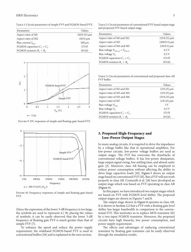
Figure 5: Output stage based on FVF [15].
M3
M1
M2
M5 M6
M4 M7
𝑉in
𝑉out
𝑉bias
Figure 6: Class AB output stage based on FVF [14].
Replacing 𝑉𝑑1
by using (12) in (8), the transfer function isgiven by
𝐴𝑉(𝑠) = (𝑟
𝑜1𝑟𝑜2(𝑠𝐶𝑔𝑠1
+ 𝑔𝑚1)𝑋
+𝑔𝑚1𝑟𝑜1𝑟𝑜2𝑅𝑏(𝑔𝑚2𝑟𝑜1𝐶1− 𝐶𝑇))
× (𝑟𝑜1𝑟𝑜2(𝑠𝐶𝑔𝑠1
+ 𝑔𝑚1)𝑋 + 𝑋 (𝑟
𝑜1+ 𝑟𝑜2)
+ 𝑔𝑚1𝑟𝑜1𝑟𝑜2𝑅𝑏(𝑔𝑚2𝑟𝑜1𝐶1− 𝐶𝑇)
+𝑟𝑜2𝑅𝑏(𝑔𝑚2𝑟𝑜1𝐶1− 𝐶𝑇))−1
,
(13)
where𝑋 = 𝐶𝑇(𝑟𝑜1+ 𝑅𝑏) + 𝑠𝐶
1𝑟𝑜1𝑅𝑏(𝐶𝑇− 𝐶1).
Assuming 𝑟𝑜1= 𝑟𝑜2= 𝑟𝑜, 𝐶1= 𝐶2= 𝐶, and 𝐶
𝑔𝑠1=
𝐶𝑔𝑠2
= 𝐶𝑔𝑠, (13) transforms into
𝐴𝑉(𝑠) =
𝑎2𝑠2+ 𝑎1𝑠 + 𝑎0
𝑎2𝑠2 + (𝑎
1+ Δ𝑎1) 𝑠 + (𝑎
0+ Δ𝑎0), (14)
M5
M1
M3
M2
M4
𝑉in
𝑉out
𝑉bias 𝑝
𝑉bias 𝑛
𝐶1
𝐶2𝑉𝑏
Figure 7: The proposed output stage based on floating gate FVF.
M3
M1
M2
M5 M6
M4 M7
𝑉in
𝑉out
𝑉bias
𝐶1
𝐶2𝑉𝑏
Figure 8:The proposed class AB output stage based on floating gateFVF.
where
𝑎2= 𝐶𝑔𝑠𝐶 (𝐶𝑔𝑠+ 𝐶) 𝑟
3
𝑜𝑅𝑏,
𝑎1= 𝑟2
𝑜{𝑔𝑚1𝑟𝑜𝑅𝑏𝐶 (𝐶𝑔𝑠+ 𝐶) + 𝐶
𝑔𝑠(𝑟𝑜+ 𝑅𝑏) (𝐶𝑔𝑠+ 2𝐶)} ,
Δ𝑎1= 2𝐶𝑅
𝑏(𝐶𝑔𝑠+ 𝐶) ,
𝑎0= 𝑔𝑚1𝑟3
𝑜(𝐶𝑔𝑠+ 2𝐶) + 𝑔
𝑚1𝑔𝑚2𝑟3
𝑜𝑅𝑏𝐶,
Δ𝑎0= {𝑔𝑚2𝑟2
𝑜𝑅𝑏𝐶 + 𝑟𝑜𝑅𝑏(𝐶𝑔𝑠+ 2𝐶) + 2𝑟
2
𝑜(𝐶𝑔𝑠+ 2𝐶)} .
(15)
By definition, at 𝜔 = 𝜔𝑜, |𝐴𝑉|2= 1/2 [16], and thus
1
2=
(𝑎0− 𝑎2𝜔2)2
+ (𝑎1𝜔)2
((𝑎0+ Δ𝑎0) − 𝑎2𝜔2) + ((𝑎
1+ Δ𝑎1) 𝜔)2. (16)
The −3 dB frequency is
𝜔0=1
𝑎2
√Δ𝑎1
2 + 2𝑎1Δ𝑎1+ 2𝑎0𝑎2− 𝑎1
2 − 2𝑎2Δ𝑎0. (17)
ISRN Electronics 5
Table 1: Circuit parameters of simple FVF and FGMOS-based FVF.
Parameters ValuesAspect ratio of M1 (10/0.25)𝜇mAspect ratio of M2 (10/1)𝜇mBias current 𝐼bias 500 𝜇AFGMOS capacitors 𝐶
1= 𝐶2
175 fFFGMOS resistors 𝑅
1= 𝑅2
10GΩ
0 0.5 1 1.5 2 2.5 30
1
2
3
(V)
Simple FVF
FGMOS-based FVF
𝑉(4)
𝑉in (V)
Figure 9: DC responses of simple and floating-gate-based FVF.
Simple FVF
FGMOS-based FVF
1 Hz 100 Hz 10 kHz 100 MHz1 MHz 10 GHzFrequency
0
−4
−2
−6
DB (𝑉(4)/𝑉1(𝑉in ))
Figure 10: Frequency responses of simple and floating-gate-basedFVF.
(Since the expression of the lower 3-dB frequency is too large,the symbols are used to represent it.) By placing the valuesof symbols, it can be easily observed that the lower 3-dBfrequency of floating gate FVF is much greater than that ofsimple FVF [7].
To enhance the speed and reduce the power supplyrequirement, the wideband FGMOS-based FVF is used inconventional buffers [14] and is explained in the next section.
Table 2: Circuit parameters of conventional FVF-based output stageand proposed FVF-based output stage.
Parameters ValuesAspect ratio of M1 and M2 (13/0.25) 𝜇mAspect ratio of M3 (100/0.5) 𝜇mAspect ratio of M4 and M5 (50/0.5) 𝜇mBias voltage 𝑉bias 𝑝 = 𝑉bias 𝑛 0.3 VBias voltage 𝑉
𝑏0.2V
FGMOS capacitors 𝐶1= 𝐶2
175 fFFGMOS resistors 𝑅
1= 𝑅2
10GΩ
Table 3: Circuit parameters of conventional and proposed class ABFVF buffer.
Parameters ValuesAspect ratio of M1 and M2 (2/0.25) 𝜇mAspect ratio of M3 and M4 (3/0.25) 𝜇mAspect ratio of M5 and M6 (15/0.25) 𝜇mAspect ratio of M7 (1/0.25) 𝜇mBias voltage 𝑉bias 1 VBias voltage 𝑉
𝑏0.2 V
FGMOS capacitors 𝐶1= 𝐶2
175 fFFGMOS resistors 𝑅
1= 𝑅2
10GΩ
3. Proposed High-Frequency andLow-Power Output Stages
In many analog circuits, it is required to drive the impedanceby a voltage buffer like that in operational amplifiers. Forlow-power circuits, low-power voltage buffers are used asoutput stages. The FVF has overcome the drawbacks ofconventional voltage buffers. It has low-power dissipation,large output signal swing, low settling time, and almost unitygain [2]. Moreover, class AB biasing can be employed toreduce power consumption without affecting the ability todrive large capacitive loads [14]. Figure 5 shows an outputstage based on conventional FVF [15]. But a FVFwill notworkproperly in class AB. Centurelli et al. [14] have developed anoutput stage which was based on FVF operating in class AB(Figure 6).
In this paper, we have introduced two output stages whichare based on FVF with FGMOS level shifter. The proposedoutput stages are shown in Figures 7 and 8.
The output stage shown in Figure 8 operates in class AB.It is shown in Section 2.2 that a FVF with a floating gate levelshifter has larger bandwidth in comparison to the conven-tional FVF. This motivates us to replace MOS transistor M2by a two-input FGMOS transistor. Moreover, the proposedcircuits have high linearity, low power consumption, andpower supply requirement.
The effects and advantages of replacing conventionaltransistor by floating gate transistor can be easily observedthrough the simulation results.
6 ISRN Electronics
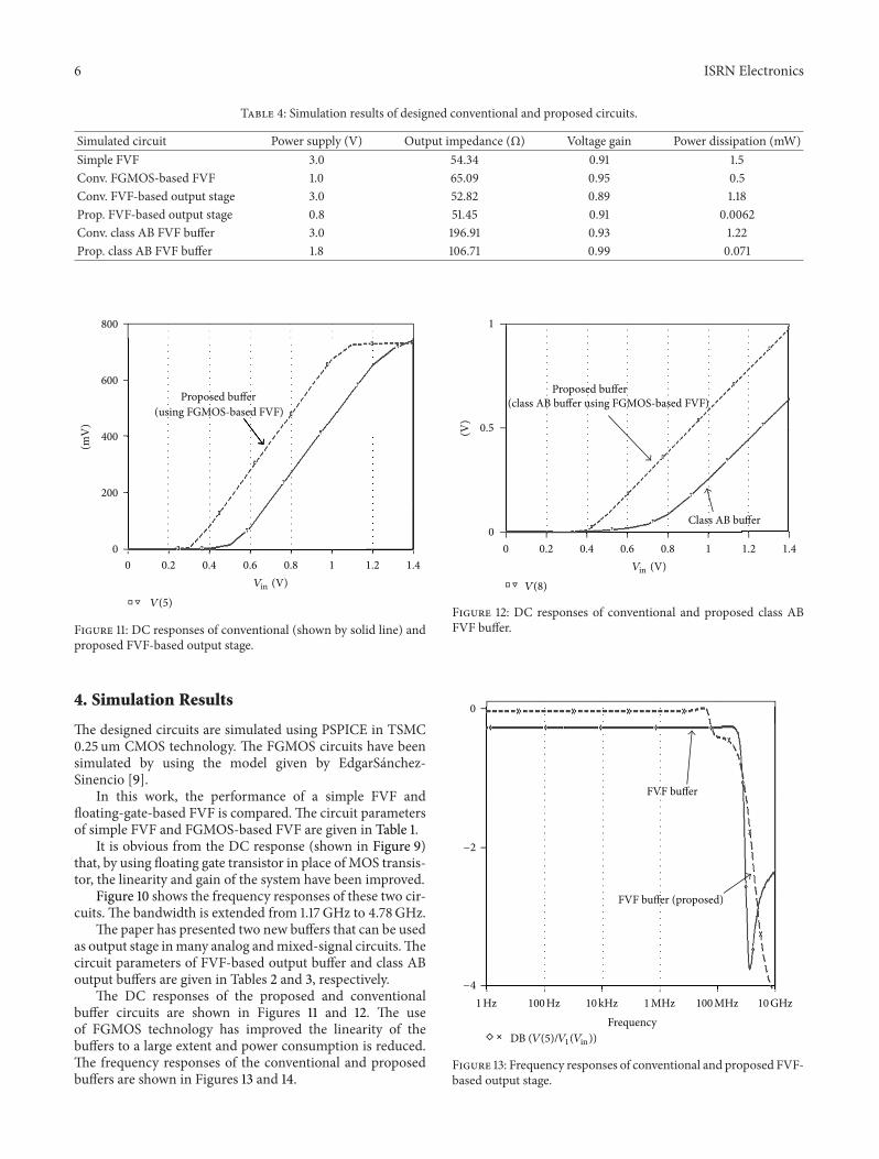
Table 4: Simulation results of designed conventional and proposed circuits.
Simulated circuit Power supply (V) Output impedance (Ω) Voltage gain Power dissipation (mW)Simple FVF 3.0 54.34 0.91 1.5Conv. FGMOS-based FVF 1.0 65.09 0.95 0.5Conv. FVF-based output stage 3.0 52.82 0.89 1.18Prop. FVF-based output stage 0.8 51.45 0.91 0.0062Conv. class AB FVF buffer 3.0 196.91 0.93 1.22Prop. class AB FVF buffer 1.8 106.71 0.99 0.071
0 0.2 0.4 0.6 0.8 1 1.2 1.40
200
400
600
800
(mV
)
Proposed buffer(using FGMOS-based FVF)
𝑉(5)
𝑉in (V)
Figure 11: DC responses of conventional (shown by solid line) andproposed FVF-based output stage.
4. Simulation Results
The designed circuits are simulated using PSPICE in TSMC0.25 um CMOS technology. The FGMOS circuits have beensimulated by using the model given by EdgarSanchez-Sinencio [9].
In this work, the performance of a simple FVF andfloating-gate-based FVF is compared. The circuit parametersof simple FVF and FGMOS-based FVF are given in Table 1.
It is obvious from the DC response (shown in Figure 9)that, by using floating gate transistor in place of MOS transis-tor, the linearity and gain of the system have been improved.
Figure 10 shows the frequency responses of these two cir-cuits. The bandwidth is extended from 1.17GHz to 4.78GHz.
The paper has presented two new buffers that can be usedas output stage inmany analog andmixed-signal circuits.Thecircuit parameters of FVF-based output buffer and class ABoutput buffers are given in Tables 2 and 3, respectively.
The DC responses of the proposed and conventionalbuffer circuits are shown in Figures 11 and 12. The useof FGMOS technology has improved the linearity of thebuffers to a large extent and power consumption is reduced.The frequency responses of the conventional and proposedbuffers are shown in Figures 13 and 14.
0 0.2 0.4 0.6 0.8 1 1.2 1.4
(V)
0
0.5
1
Proposed buffer(class AB buffer using FGMOS-based FVF)
Class AB buffer
𝑉(8)
𝑉in (V)
Figure 12: DC responses of conventional and proposed class ABFVF buffer.
0
FVF buffer (proposed)
FVF buffer
1 Hz 100 Hz 10 kHz 100 MHz1 MHz 10 GHzFrequency
−2
−4
DB (𝑉(5)/𝑉1(𝑉in ))
Figure 13: Frequency responses of conventional and proposed FVF-based output stage.

ISRN Electronics 7
1 Hz
100 H
z
10 H
z
10 kH
z
100 k
Hz
1 kH
z
100 M
Hz
10 M
Hz
1 MH
z
10 G
Hz
1 GH
z
Frequency
0
Class AB FVF buffer (proposed)
Class AB FVF buffer (conventional)
−1
−2
−3
DB (𝑉(8)/𝑉1(𝑉in ))
Figure 14: Frequency responses of conventional and proposed classAB buffers.
The level shifting in output signal can be easily observedin the proposed circuits. The bandwidth has been largelyenhanced by using floating-gate-based FVF.The comparativeresults are given in Table 4.
5. Conclusion
In this paper, two new low-power low-voltage and widebandoutput stages based on FVF with floating gate level shifterhave been proposed. The use of floating gate technologyprovides the advantages of low-power consumption and low-power supply requirement. Moreover it gives a significantimprovement in the bandwidth of the systems and the abilityof the buffers to drive heavy capacitive loads by decreasingthe output impedance. The simulation results have shownthat the proposed buffers display good characteristics whencompared with the reported works achieved so far. Theseimproved buffer structures can be useful as output stage inmany analog signal processing applications.
References
[1] S. S. Mohan, M. del Mar Hershenson, S. P. Boyd, and T. H.Lee, “Bandwidth extension in CMOS with optimized on-chipinductors,” IEEE Journal of Solid-State Circuits, vol. 35, no. 3, pp.346–355, 2000.
[2] R. G. Carvajal, J. Ramirez-Angulo, A. L. Martin et al., “Theflipped voltage follower: a useful cell for low voltage low powercircuit design,” IEEE Transactions on Circuits and Systems I, vol.52, no. 7, pp. 1276–1279, 2005.
[3] J. Ramırez-Angulo, S. Gupta, I. Padilla et al., “Comparison ofconventional and new flipped voltage structures with increasedinput/output signal swing and current sourcing/sinking capa-bilites,” in Proceedings of the IEEE International 48th Midwest
Symposium on Circuits and Systems (MWSCAS ’05), pp. 1151–1154, August 2005.
[4] J. Ramirez-Angulo, R. G. Carvajal, A. Torralba, J. Galan, A. P.Vega-Leal, and J. Tombs, “Low-power low-voltage analog elec-tronic circuits using the flipped voltage follower,” in Proceedingsof the IEEE International Symposium on Industrial Electronics,pp. 1327–1330, May 2002.
[5] C. Sakul and K. Dejhan, “Squaring and square-root circuitsbased on flipped voltage follower and applications,” Interna-tional Journal of Information Systems and TelecommunicationEngineering, vol. 1, pp. 19–24, 2010.
[6] C. Koliopoulos and C. Psychalinos, “A comparative study of theperformance of the flipped voltage follower based low-voltagecurrent mirrors,” in Proceedings of the International SymposiumOn Signals, Circuits and Systems (ISSCS ’07), vol. 1, pp. 1–4, Iasi,Romania, July 2007.
[7] M. Gupta and U. Singh, “A new flipped voltage followerwith enhanced bandwidth and low output impedance,” AnalogIntegrated Circuits & Signal Processing, vol. 72, no. 1, pp. 279–288, 2012.
[8] E. R. Villegas, Low Power and Low Voltage Circuit DesignWith the FGMOS Transistor, IEE Circuits, Devices and SystemsSeries,The Institution of Engineering and Technology, London,UK, 2006.
[9] E. Sanchez-Sinencio, “Floating Gate Techniques and Appli-cations,” 2012, http://amesp02.tamu.edu/∼sanchez/607-2010-Floating%20Gate%20Circuits.pdf.
[10] S. S. Rajput and S. S. Jamuar, “Design techniques for low voltageanalog circuit structures,” in Proceedings of the IEEE NationalSymposiumon Microelectronic (NSM ’01), pp. 49–52, GentingHighlands, Malaysia, 2001.
[11] S. Sharma, S. S. Rajput, L. K. Mangotra, and S. S. Jamuar,“FGMOS current mirror: behaviour and bandwidth enhance-ment,” Analog Integrated Circuits & Signal Processing, vol. 46,no. 3, pp. 281–286, 2006.
[12] A. J. Lopez-Martin, J. Ramırez-Angulo, R. G. Carvajal, and L.Acosta, “CMOS transconductors with continuous tuning usingFGMOSbalanced output current scaling,” IEEE Journal of Solid-State Circuits, vol. 43, no. 5, pp. 1313–1323, 2008.
[13] R. Pandey and M. Gupta, “FGMOS based tunable groundedresistor,” Analog Integrated Circuits & Signal Processing, vol. 65,no. 3, pp. 437–443, 2010.
[14] F. Centurelli, P. Monsurro, and A. Trifiletti, “A class-AB flippedvoltage follower output stage,” in Proceedings of the 20th Euro-pean Conference on Circuit Thoery and Design (ECCTD ’11), pp.757–760, Rome, Italy, 2011.
[15] M. Jimenez, A. Torralba, R. G. Carvajal, and J. Ramirez-Angulo,“A new low-voltage CMOS unity-gain buffer,” in Proceedings ofthe 2006 IEEE International Symposium on Circuits and Systems(ISCAS ’06), pp. 919–922, May 2006.
[16] A. S. Sedra and K. C. Smith, Microelectronics Circuits, OxfordUniversity Press, New York, NY, USA, 5th edition, 2005.

Submit your manuscripts athttp://www.hindawi.com
VLSI Design
Hindawi Publishing Corporationhttp://www.hindawi.com Volume 2014
International Journal of
RotatingMachinery
Hindawi Publishing Corporationhttp://www.hindawi.com Volume 2014
Hindawi Publishing Corporation http://www.hindawi.com
Journal ofEngineeringVolume 2014
Hindawi Publishing Corporationhttp://www.hindawi.com Volume 2014
Shock and Vibration
Hindawi Publishing Corporationhttp://www.hindawi.com Volume 2014
Mechanical Engineering
Advances in
Hindawi Publishing Corporationhttp://www.hindawi.com Volume 2014
Civil EngineeringAdvances in
Acoustics and VibrationAdvances in
Hindawi Publishing Corporationhttp://www.hindawi.com Volume 2014
Hindawi Publishing Corporationhttp://www.hindawi.com Volume 2014
Electrical and Computer Engineering
Journal of
Hindawi Publishing Corporationhttp://www.hindawi.com Volume 2014
Distributed Sensor Networks
International Journal of
The Scientific World JournalHindawi Publishing Corporation http://www.hindawi.com Volume 2014
SensorsJournal of
Hindawi Publishing Corporationhttp://www.hindawi.com Volume 2014
Modelling & Simulation in EngineeringHindawi Publishing Corporation http://www.hindawi.com Volume 2014
Hindawi Publishing Corporationhttp://www.hindawi.com Volume 2014
Active and Passive Electronic Components
Hindawi Publishing Corporationhttp://www.hindawi.com Volume 2014
Chemical EngineeringInternational Journal of
Control Scienceand Engineering
Journal of
Hindawi Publishing Corporationhttp://www.hindawi.com Volume 2014
Antennas andPropagation
International Journal of
Hindawi Publishing Corporationhttp://www.hindawi.com Volume 2014
Hindawi Publishing Corporationhttp://www.hindawi.com Volume 2014
Navigation and Observation
International Journal of
Advances inOptoElectronics
Hindawi Publishing Corporation http://www.hindawi.com
Volume 2014
RoboticsJournal of
Hindawi Publishing Corporationhttp://www.hindawi.com Volume 2014