high frequency, high current 3d integrated point-of-load ...€¦ · high frequency, high current...
TRANSCRIPT

High Frequency, High Current 3D Integrated
Point-of-Load Module
Yipeng Su
Dissertation submitted to the Faculty of the
Virginia Polytechnic Institute and State University
in partial fulfillment of the requirements for the degree of
Doctor of Philosophy
in
The Bradley Department of Electrical and Computer Engineering
Fred C. Lee, Chair
Dong S. Ha
Michael S. Hsiao
Qiang Li
Kathy P. Lu
October 2nd
, 2014
Blacksburg, Virginia
Keywords: POL converter, 3D integration, planar inductor substrate, non-uniform
flux, LTCC, PCB embedded inductor.
© 2014, Yipeng Su

High Frequency, High Current 3D Integrated
Point-of-Load Module
Yipeng Su
Abstract
Point-of-load (POL) converters have been used extensively in IT products. Today, almost
every microprocessor is powered by a multi-phase POL converter with high output current,
which is also known as voltage regulator (VR). In the state-of-the-art VRs, the circuits are
mostly constructed with discrete components and situated on the motherboard, where it can
occupy more than 1/3 of the footprint of the motherboard. A compact POL is desirable to save
precious space on motherboards to be used for some other critical functionalities. Recently,
industry has released many modularized POL converters, in which the bulky inductor is
integrated with the active components to increase the power density. This concept has been
demonstrated at current levels less than 5A and power density around 600-1000W/in3. This
might address the needs of small hand-held equipment such as smart phones, but it is far from
meeting the needs for the applications such as laptops, desktops and servers, where tens and
hundreds of amperes are needed.
A 3D integrated POL module with an output current of tens of ampere has been successfully
demonstrated at the Center for Power Electronic Systems (CPES), Virginia Tech. In this
structure, the inductor is elaborated with low temperature co-fire ceramic (LTCC) ferrite, as a
substrate where the active components are placed. The lateral flux inductor is proposed to

iii
achieve both a low profile and high power density. Generally, the size of the inductor can be
continuously shrunk by raising the switching frequency. The emerging gallium-nitride (GaN)
power devices enable the creation and use of a multi-MHz, high efficiency POL converter. This
dissertation firstly explores the LTCC inductor substrate design in the multi-MHz range for a
high-current POL module with GaN devices. The impacts of different frequencies and different
LTCC ferrite materials on the inductor are also discussed. Thanks to the DC flux cancellation
effect, the inverse coupled inductor further improves the power density of a 20A, 5MHz two-
phase POL module to more than 1kW/in3. An FEA simulation model is developed to study the
core loss of the lateral flux coupled inductor, which shows the inverse coupling is also beneficial
for core loss reduction.
The ceramic-based 3D integrated POL module, however, is not widely adopted in industrial
products because of the relatively high cost of the LTCC ferrite material and complicated
manufacturing process. To solve that problem, a printed circuit board (PCB) inductor substrate
with embedded alloy flake composite core is proposed. The layerwise magnetic core is laminated
into a multi-layer PCB, and the winding of the inductor then is formed by the copper layers and
conventional PCB vias. As a demonstration of system integration, a 20A, 1.5MHz integrated
POL module is designed and fabricated based on a 4-layer PCB with embedded flake core,
which realizes more than 85% efficiency and 600W/in3 power density. The application of
standardized PCB processes reduces the cost for manufacturing the integrated modules due to the
easy automation and the low temperature manufacturing process. Combining the PCB-embedded
coupled inductor substrate and advanced control strategy, the two-phase 40A POL modules are
elaborated as a complete integrated laptop VR solution. The coupled inductor structure is slightly
modified to improve its transient performance. The nonlinearity of the inductance is controlled

iv
by adding either air slots or low permeability magnetic slots into the leakage flux path of the
coupled inductor. Then the leakage flux, which determines the transient response of the coupled
inductor, can be well controlled. If we directly replace the discrete VR solution with the
proposed integrated modules, more than 50% of the footprint on the motherboard can be saved.
Although the benefits of the lateral flux inductor have been validated in terms of its high
power density and low profile, the planar core is excited under very non-uniform flux. Some
parts of the core are even pushed into the saturation region, which totally goes against the
conventional sense of magnetic design. The final part of this dissertation focuses on evaluating
the performance of the planar core with variable flux. The counterbalance between DC flux and
AC flux is revealed, with which the AC flux and the core loss density are automatically limited
in the saturated core. The saturation is essentially no longer detrimental in this special structure.
Compared with the conventional uniform flux design, the variable flux structure extends the
operating point into the saturation region, which gives better utilization of the core. In addition,
the planar core with variable flux also provides better thermal management and more core loss
reduction under light load.
As conclusions, this research first challenges the conventional magnetic design rules, which
always assumes uniform flux. The unique characteristics and benefits of the variable flux core
are proved. As an example of taking advantages of the lateral flux inductor, the PCB integrated
POL modules are proposed and demonstrated as a high-density VR solution. The integrated
modules are cost-effective and ready to be commercialized, which could enable the next
technological innovation for the whole computing and telecom industry.

Yipeng Su
v
TO MY FAMILY:
My parents: Xinyou Su and Shimei Jiang
My parents in law: Fansen Kong and Yuchun Liu
My Wife: Na Kong
My son: Daniel Su

Yipeng Su Acknowledgments
vi
Acknowledgments
With sincere appreciation in my heart, I would like to thank my advisor, Professor Fred C.
Lee, for his continuous guidance, encouragement and support during my journey toward the
Ph.D. degree. Dr. Lee has watched every step and every improvement that I have made in past
five years like a parent. Of many valuable things I have learned from him, his attitude toward
research, “never stop challenging yourself”, is the most precious one for me, and is going to
benefit me in the rest of my life. I would also like to give specific appreciation to Professor
Qiang Li. As my mentor when I just entered CPES, he helped me find out the right track of my
research with his selfless friendship and leadership. Besides many technical skills, he also
showed me an excellent model as a diligent and insightful researcher.
It is an honor for me to have Professor Dong S. Ha, Professor Michael S. Hsiao and
Professor Kathy P. Lu as my committee members. I am truly thankful to them for all technical
discussions, opinions and suggestions as well as for the shared knowledge in the different areas
of power electronics.
A lot of work in this dissertation is team efforts. I am grateful to every members in VRM
group including Mr. David Gilham who helped LTCC inductor fabrication; Dr. Wenli Zhang
who helped PCB embedded core fabrication; Dr. David Reusch and Mr. Shu Ji who helped the
active layer design for the POL modules with GaN devices; Dr. Mingkai Mu and Dr. Dongbin
Hou who helped the inductor loss testing; Mr. Pei-Hsin Liu who helped the evaluation on the
transient performance of the inductors; Mr. Shuojie She who helped the FEA thermal simulation.
Without your help, this dissertation even would not have been possible.

Yipeng Su Acknowledgments
vii
I would like to thank colleagues in the power management consortium (PMC) of CPES.
It is my honor to work with these talented, creative, helpful and dedicated people: Dr. Ming Xu,
Dr. Shuo Wang, Dr. Jian Li, Dr. Chuanyun Wang, Dr. Yan Dong, Dr. Dianbo Fu, Dr. Pengju
Kong, Mr. Zheng Luo, Dr. Daocheng Huang, Mr. Pengjie Lai, Mr. Zijian Wang, Mr. Qian Li, Dr.
Yingyi Yan, Mr. Feng Yu, Mr. Haoran Wu, Mr. Chanwit Prasantanakorn, Dr. Weiyi Feng, Mr.
Shuilin Tian, Mr. Wei Zhang, Mr. Li Jiang, Mr. Pei-Hsin Liu, Mr. Xiucheng Huang, Mr.
Zhengyang Liu, Mr. Yuchen Yang. Mr. Chao Fei, Mr. Xuebin Chen, Mr. Syed Bari, Mr.
Zhongsheng Cao, Mr. Bin Li, Mr. Tao Liu, Ms. Yincan Mao, Ms. Virginia Li.
I also appreciate all other colleagues and students outside PMC at CPES: Dr. Fang Luo,
Dr. Di Zhang, Dr. Puqi Ning, Mr. Igor Cvetkovic, Dr. Dong Dong, Dr. Ruxi Wang, Dr. Dong
Jiang, Dr. Zheng Chen, Dr. Sara Ahmed, Dr. Zhiyu Shen, Dr. Xuning Zhang, Dr. Zhuxian Xu,
Dr. Jing Xue, Dr. Zheng Zhao, Mr. Bo Wen, Mr. Marko Jaksic, Mr. Milisav Danilovic, Mr.
Lingxiao Xue, Mr. Bo Zhou, Dr. Hemant Bishnoi, Mr. Yang Jiao, Ms. Christina DiMarino, Mr.
Jun Wang, Mr. Qiong Wang, Mr. Shishuo Zhao, Mr. Li Jiang, Mr. Yin Wang, Ms. Han Cui, Mr.
Woochan Kim, Mr. Tao Tao, Mr. Di Xu, Mr. Kumar Gandharva, Mr. Zhemin Zhang, Mr.
Hanguang Zheng, Dr. Yiying Yao, Mr. Ming Lu, Mr. Ting Ge. It is precious memory to live and
work with you in the past five years.
Many visiting scholars have brought their expertise and helpful discussion during my
research. They are Dr. Kuang-Yao Cheng, Dr. Xiaoyong Ren, Dr. Qiaoliang Chen, Dr. Yue
Chang, Dr. Feng Zheng, Dr. Xinke Wu, Dr. Weijun Lei, Mr. Zeng Li, Dr. Jin Li, Dr. Montiê
Vitorino, Dr. Feng Wang, Dr. Hao Zhang, Dr. Weijing Du, Mr. Peiqing Hu. Thank you for the
help and friendship.

Yipeng Su Acknowledgments
viii
I would also like to thank the wonderful members of the CPES staffs who were always
willing to help me: Ms. Teresa Shaw, Ms. Linda Gallagher, Ms. Teresa Rose, Ms. Marianne
Hawthorne, Ms. Linda Long, Mr. Douglas Sterk.
Finally but not the least, I would like to thank my families with deepest love, my parents
Xinyou Su and Shimei Jiang, my wife Na Kong, who have always been there with their love,
support, understanding and encouragement for all of my endeavors.
This work was supported by the Power Management Consortium at CPES (Chicony
Power, Delta Electronics, Huawei Technologies, International Rectifier, Linear Technology,
Texas Instruments, NEC/TOKIN Corporation, Richtek Technology, Murata Manufacturing Co.,
Ltd., NXP Semiconductors, 3M Company, CSR Zhuzhou Institute Co., Ltd., Macroblock, Inc.,
Altera-Enpirion Power, Eltek), and APRA-E under the “Power Supplies on a Chip (PSOC)”
project (DE-AR00000106).
The author would like to thank NEC/Tokin for providing the SENFOLIAGE flake
composite material, Isola for providing FR4 materials, and all the technical supports from them.

Yipeng Su List of Contents
ix
Table of Contents
Chapter 1. Introduction ..................................................................................... 1
1.1 Review of the State-of-the-Art POL Module ........................................................ 1
1.2 High-Frequency Switching Technologies ............................................................. 8
1.2.1 Advanced semiconductor devices ........................................................................ 8
1.2.2 Improved active devices packaging ................................................................... 11
1.3 High-Frequency Integratable Magnetic Materials ............................................ 15
1.4 3D Integration with DBC Carrier and LTCC Inductor Substrate .................. 23
1.5 Planar Inductors for the High-Current 3D Integrated POL Modules ............ 27
1.6 Challenges for the Remaining Problems............................................................. 32
1.7 Dissertation Outline .............................................................................................. 34
Chapter 2. Multi-MHz Single Phase LTCC Inductor Substrate ................ 37
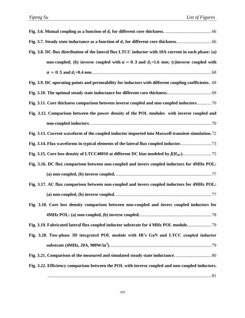
2.1 High Frequency POL converter with GaN Devices ........................................... 37
2.2 High Frequency LTCC Ferrite Material Comparison ...................................... 41
2.3 Single-Phase LTCC Inductor Substrate Design ................................................ 42
2.3.1 Design the dimensions of the LTCC inductor. ................................................... 46
2.3.2 Inductor loss calculation ................................................................................... 48
2.3.3 Choosing the number of turns (N) ..................................................................... 50
2.4 Fabrication and Evaluation of the LTCC inductor Substrates ........................ 52

Yipeng Su List of Contents
x
2.5 Summary ................................................................................................................ 58
Chapter 3. FEA Modeling of the Lateral Flux Coupled Inductor .............. 59
3.1 Challenges to Model the Lateral Flux Coupled Inductor ................................. 59
3.2 Inductance Modeling ............................................................................................ 62
3.3 Core Loss Modeling .............................................................................................. 71
3.4 Experimental Verification of the FEA Models ................................................... 78
3.5 Summary ................................................................................................................ 81
Chapter 4. 3D Integrated POL Module with PCB Embedded Inductor
Substrate ........................................................................................ 83
4.1 Review of the PCB Substrates with Embedded Core ........................................ 83
4.2 PCB Embedded Core with NEC/Tokin’s Metal Flake Composite ................... 87
4.3 High Density POL Module with PCB Integrated Inductor Substrate ............. 95
4.3.1 Two-layer PCB Based Inductor Substrates with Embedded SF Flake Core ..... 95
4.3.2 Four-layer PCB Based Integrated POL Module with Embedded SF Flake Core .
........................................................................................................................... 99
4.4 Evaluation of the PCB Integrated POL Modules ............................................ 103
4.5 Summary .............................................................................................................. 111
Chapter 5. Lateral Flux Coupled Inductor with Transient Improvement ....
.................................................................................................. 112

Yipeng Su List of Contents
xi
5.1 Evaluation of the Transient Response of Previous Coupled Inductor ........... 112
5.2 New Lateral Flux Coupled Inductor with Transient Improvement .............. 119
5.3 Experimental Verification of the Proposed Structure ..................................... 128
5.4 Two-Phase Integrated POL Module with PCB Embedded Coupled Inductor
Substrate ............................................................................................................. 132
5.5 Summary .............................................................................................................. 137
Chapter 6. Fundamental Study of the Planar Core with Variable Flux .. 138
6.1 Non-uniform Flux Distribution in Lateral Flux Planar Inductor .................. 138
6.2 Evaluation of the Core Utilization ..................................................................... 145
6.3 Thermal Evaluation of the Planar Core with Variable Flux .......................... 148
6.4 Comparison between the Variable Flux Core and the Uniform Flux Core .. 153
6.5 Summary .............................................................................................................. 158
Chapter 7. Conclusions and Future Work .................................................. 160
7.1 Conclusions .......................................................................................................... 160
7.2 Future Work ........................................................................................................ 164
Reference ...................................................................................................... 165

Yipeng Su List of Figures
xii
List of Figures
Fig. 1.1. Power density of state-of-the-art POL converters [2]-[9]. ........................................................ 2
Fig. 1.2. SIMPLE SWITCHER® nano POL module with 1A maximum output current by TI [2]: (a)
conceptual drawing, (b) prototypes showing actual size. ........................................................ 3
Fig. 1.3. LXDC55K µDCDC converter with 3A maximum output current by Murata [3]: (a) ferrite
substrate developed by multilayer process, (b) prototypes showing actual size. ................... 3
Fig. 1.4. EN5366Q POL module with 6A maximum output current by Enpirion [4]: (a) internal
structure showing a low-profile MEMS inductor on top of silicon [10]; (b) prototype
showing actual size. ..................................................................................................................... 4
Fig. 1.5. LTM4627 capsulated POL module with 15A Iout by Linear Technology [6]: (a) top view of
X-ray picture self-made, (b) side view of X-ray picture self-made, (c) prototype with
marked dimensions. .................................................................................................................... 5
Fig. 1.6. Voltage regulators (VRs) occupy more than 30% of the real estate of the motherboard in
desktops. ....................................................................................................................................... 7
Fig. 1.7. High current POL modules with discrete components: (a) product from Murata Power
Solutions with 20A maximum output current [7], (b) product from Delta Electronics with
maximum 30A output current [8]. ............................................................................................. 8
Fig. 1.8. Operating frequency and current capability for different semiconductor devices. ............. 10
Fig. 1.9 Typical packaging technologies used in commercial low voltage power MOSFETs: (a) SO-8
[28], (b) LFPAK [28], (c) DirectFET [30]. .............................................................................. 11
Fig. 1.10 Typical packaging technologies used in lateral devices [27]: (a) ball grid array (BGA), (b)
linear grid array (LGA). ........................................................................................................... 13
Fig. 1.11. Different DrMOS packaging structures used by industry: (a) product from Fairchild [32],
(b) product from International Rectifier [33], (c) product from Texas Instruments [34]. . 13

Yipeng Su List of Figures
xiii
Fig. 1.12. Switching loss breakdown for a POL converter with same dies but different packagings.
.................................................................................................................................................... 15
Fig. 1.13. Roadmap for high frequency magnetic materials in terms of core loss density as a
function of frequency ................................................................................................................ 16
Fig. 1.14. Integrated inductor on PCB substrate with electroplated NiFe demonstrated by Tyndall
[39] (a) half 3D view of the winding and core structure, (b) POL module on the integrated
inductor substrate. .................................................................................................................... 18
Fig. 1.15. Integrated inductor on silicon substrate with electroplated NiFe demonstrated by Tyndall
[41] (a) cross-sectional view of the winding and core structure, (b) top view of the micro-
inductor. ..................................................................................................................................... 18
Fig. 1.16. V-groove on chip inductor with large copper cross-sectional area to improve current
capability of the on-chip inductor demonstrated by Dartmouth College [42]. .................... 19
Fig. 1.17. Cross section view of the micro structure for different metal flake composites (a) material
developed by University of Delaware [43], (b) material developed by NEC/Tokin [44]..... 21
Fig. 1.18. A 60W integrated converter based on FPC core embedded in PCB [45]. ........................... 22
Fig. 1.19. Basic structure of the 3D integration. ..................................................................................... 23
Fig. 1.20. The first generation of the 3D integrated POL module with LTCC inductor substrate
developed by CPES [47]: (a) the conceptual drawing, (b) the prototype. ............................ 24
Fig. 1.21. The second generation of the 3D integrated POL module with LTCC inductor substrate
developed by CPES [47]. .......................................................................................................... 25
Fig. 1.22. The active layer design for the third generation of the 3D integrated POL module at
CPES [57]. .................................................................................................................................. 26
Fig. 1.23. The prototype of the third generation 3D integrated POL module. .................................... 26
Fig. 1.24. The fourth generation of the 3D integrated POL module with an LTCC inverse coupled
inductorwith lateral flux pattern [58]. .................................................................................... 27

Yipeng Su List of Figures
xiv
Fig. 1.25. Basic unit cells for different planar inductors: (a) vertical flux inductor, (b) lateral flux
inductor. ..................................................................................................................................... 27
Fig. 1.26. Real implementation of the vertical flux inductor in [47]. .................................................... 29
Fig. 1.27. Real implementation of the LTCC lateral flux inductor in [21]: (a) single-turn structure,
(b) two-turn structure, (c) three-turn structure. .................................................................... 29
Fig. 1.28. Prototypes comparison between the lateral flux inductor and vertical flux inductor [21].30
Fig. 1.29. Two-phase invers coupled inductors with a lateral flux pattern [21]. ................................. 31
Fig. 1.30. Power density achievements of the 3D integrated POL modules with LTCC inductor
substrates developed by CPES [2]-[9]. .................................................................................... 31
Fig. 2.1. Available low voltage GaN devices for POL applications: (a) EPC’s enhancement mode
GaN [25]; (b) IR’s depletion mode GaN module [26]. ........................................................... 38
Fig. 2.2. Typical driving signals for different GaN devices: (a) EPC’s enhancement mode GaNs [27];
(b) IR’s depletion mode GaN module [66]. ............................................................................. 39
Fig. 2.3. Different generations of high frequency POL converter with EPC’s GaN developed by
CPES [27]. .................................................................................................................................. 40
Fig. 2.4. Efficiency comparison of the different generations of POL converter [27]. ......................... 40
Fig. 2.5. Incremental permeability as a function of HDC for different LTCC ferrite materials. ........ 41
Fig. 2.6. Core loss density comparison for different LTCC ferrite materials. .................................... 42
Fig. 2.7. The active layer of the high frequency POL module with EPC’s discrete GaN: (a) top view;
(b) bottom view [69]. ................................................................................................................. 43
Fig. 2.8. The active layer of the high frequency POL module with IR’s monolithic GaN: (a) top view;
(b) bottom view [70]. ................................................................................................................. 43
Fig. 2.9. Lateral flux LTCC inductor substrate with dimensional parameters to be designed: (a) 3D
view of the single-turn structure; (b) top view of multi-turn structure. .............................. 44
Fig. 2.10. DC flux distribution in single-turn LTCC inductor substrate with 15A DC input current.
.................................................................................................................................................... 44

Yipeng Su List of Figures
xv
Fig. 2.11. Core thickness as a function of frequency for different number of turns. .......................... 47
Fig. 2.12. Winding DCR loss as a function of frequency for different number of turns. ................... 48
Fig. 2.13. Winding ACR loss as a function of frequency for different number of turns. ................... 49
Fig. 2.14. Core loss as a function of frequency for different number of turns. ................................... 49
Fig. 2.15. Inductor total loss as a function of frequency for different number of turns. .................... 50
Fig. 2.16. 3-turn LTCC inductor substrates working at 1MHz, 2MHz and 3MHz. ........................... 52
Fig. 2.17. 3-turns LTCC inductor substrate with surface winding: (a) top view, (b) bottom view. .. 53
Fig. 2.18. The inductance of the LTCC inductors at different DC current. ........................................ 53
Fig. 2.19. High frequency POL module with different inductors: (a) POL module with LTCC
inductor, (b) POL module with discrete inductor. ................................................................. 54
Fig. 2.20. Measured converter efficiency of the POL module with EPC’s GaN devices. ................... 55
Fig. 2.21. 3D integrated POL module with IR’s GaN devices and 2-turn LTCC inductor substrate:
(a) top view of 2-turn LTCC inductor; (b) bottom view of 2-turn LTCC inductor; (c)
integrated POL module. ........................................................................................................... 56
Fig. 2.22. Measured converter efficiency of the POL module with IR’s GaN and 2-turn LTCC
inductor. ..................................................................................................................................... 56
Fig. 2.23. Comparison of the high frequency POL module with different inductor structures. ........ 57
Fig. 3.1. Lateral flux inverse coupled inductor substrate with N=2. .................................................... 60
Fig. 3.2. Field distribution in a lateral flux coupled inductor with 10A DC current in each phase
(top view): (a) DC magnetic intensity (HDC); (b) Incremental permeability ....................... 60
Fig. 3.3. Fundamental principle of FEA simulation to model the magnetic core with non-uniform
flux. ............................................................................................................................................. 61
Fig. 3.4. Nonlinear relationship between the exciting current and total flux coupled with excitation
for the LTCC inductor. ............................................................................................................ 63
Fig. 3.5. Two steps of magneto static simulation to calculate the AC flux at a given DC operating
point: (a) step one; (b) step two ............................................................................................... 64
Yipeng Su List of Figures
xvi
Fig. 3.6. Mutual coupling as a function of dL for different core thickness. .......................................... 66
Fig. 3.7. Steady state inductance as a function of dL for different core thickness. .............................. 66
Fig. 3.8. DC flux distribution of the lateral flux LTCC inductor with 10A current in each phase: (a)
non-coupled; (b) inverse coupled with 𝜶 = 𝟎. 𝟑 and dL=1.6 mm; (c)inverse coupled with
𝜶 = 𝟎. 𝟓 and dL=0.4 mm. ........................................................................................................... 68
Fig. 3.9. DC operating points and permeability for inductors with different coupling coefficients. . 68
Fig. 3.10. The optimal steady state inductance for different core thickness. ....................................... 69
Fig. 3.11. Core thickness comparison between inverse coupled and non-coupled inductors. ............ 70
Fig. 3.12. Comparison between the power density of the POL modules with inverse coupled and
non-coupled inductors. ............................................................................................................. 70
Fig. 3.13. Current waveform of the coupled inductor imported into Maxwell transient simulation. 72
Fig. 3.14. Flux waveforms in typical elements of the lateral flux coupled inductor. ........................... 73
Fig. 3.15. Core loss density of LTCC40010 at different DC bias modeled by f(HDC). ......................... 75
Fig. 3.16. DC flux comparison between non-coupled and invers coupled inductors for 4MHz POL:
(a) non-coupled, (b) inverse coupled. ...................................................................................... 77
Fig. 3.17. AC flux comparison between non-coupled and invers coupled inductors for 4MHz POL:
(a) non-coupled, (b) inverse coupled. ...................................................................................... 77
Fig. 3.18. Core loss density comparison between non-coupled and invers coupled inductors for
4MHz POL: (a) non-coupled, (b) inverse coupled. ................................................................ 78
Fig. 3.19. Fabricated lateral flux coupled inductor substrate for 4 MHz POL module. ..................... 79
Fig. 3.20. Tow-phase 3D integrated POL module with IR’s GaN and LTCC coupled inductor
substrate (4MHz, 20A, 900W/in3). ........................................................................................... 79
Fig. 3.21. Comparison of the measured and simulated steady state inductance. ................................ 80
Fig. 3.22. Efficiency comparison between the POL with inverse coupled and non-coupled inductors.
.................................................................................................................................................... 81

Yipeng Su List of Figures
xvii
Fig. 3.23. Power density achievements of the POL modules with GaN devices and LTCC inductor
substrates. .................................................................................................................................. 82
Fig. 4.1. Multi-layer PCB substrate with embedded layerwise magnetic core [45]. ........................... 84
Fig. 4.2. Resonate DC-DC converter with PCB integrated transformer substrate [45]: (a) prototype,
(b) cross sectional view of the embedded magnetic layer and windings. ............................. 85
Fig. 4.3. SENFOLIAGE metal flake composite plates developed by NEC/Tokin. .............................. 87
Fig. 4.4. Aligning and binding processes for the SENFOLIAGE metal flake composite. .................. 88
Fig. 4.5. Cross section view of the microstructure for different metal flake composites (a) material
developed by University of Delaware [43], (b) material developed by NEC/Tokin [44]..... 88
Fig. 4.6. The comparison of high frequency core loss density for different integratable magnetic
materials. .................................................................................................................................... 89
Fig. 4.7. Incremental permeability comparison of the SF flake, UD’s flake and LTCC50 ferrite. ... 89
Fig. 4.8. Laminating structure of PCB with embedded metal flake composite core. .......................... 90
Fig. 4.9. Recommended heat and pressure profile by Isola for laminating multi-layer PCBs. .......... 91
Fig. 4.10. Cross section of PCB embedded SF flake core after conventional PCB laminating process.
.................................................................................................................................................... 92
Fig. 4.11. Magnetic components built by SF metal flake composite: (a) PCB embedded core, (b)
PCB embedded core with vias, (c) 1-turn PCB inductor, (c) 1-turn bare inductor. ........... 93
Fig. 4.12. Core loss comparison between PCB embedded inductor and bare inductor. ..................... 94
Fig. 4.13. Inductance comparison between PCB embedded inductor and bare inductor. ................. 94
Fig. 4.14. Proposed lateral flux PCB inductor substrate with embedded SF flake composite core. .. 95
Fig. 4.15. The fabrication process of the vias through PCBs with embedded core: (a) 2-layer PCB
with embedded core, (b) first drilling with larger hole size, (c) filling epoxy into the hole,
(d) second drilling with smaller hole size, (c) electroplating copper to form the via. ......... 96
Fig. 4.16. 2-turn PCB inductor substrate with embedded SF flake composite core: (a) conceptual
drawing, (b) fabricated prototype. .......................................................................................... 98

Yipeng Su List of Figures
xviii
Fig. 4.17. Measured inductance of the #1 PCB inductor compared with calculated inductance. ...... 98
Fig. 4.18. The expanded view of the 4-layer PCB structure for the 3D integrated POL module with
embedded core. ........................................................................................................................ 100
Fig. 4.19. High frequency 3D integrated POL module with PCB embedded inductor substrate. ... 102
Fig. 4.20. Cross sectional view of the 4-layer PCB with embedded magnetic layer. ......................... 102
Fig. 4.21. Cross section of multi-layer evaluation board showing PCB trace and dielectric
thicknesses [84]. ....................................................................................................................... 103
Fig. 4.22. Evaluation motherboard with mounted integrated POL module. ..................................... 104
Fig. 4.23. Measured efficiency and calculated power density of the integrated POL modules
working at different frequency (when Vin=12V, Vout=1.2V)............................................. 104
Fig. 4.24. Measured efficiency and calculated power density of the integrated POL modules
working at different frequency (when Vin=12V, Vout=1.8V)............................................. 105
Fig. 4.25. Measured external temperature of the module working at fs=1.5MHz, Vin=12V and
Vout=1.2V: (a) 15A load current with 2.8W total power loss, (b) 20A load current with
4.3W total power loss. ............................................................................................................. 106
Fig. 4.26. FEA steady state simulation model for the POL module mounted on evaluation
motherboard: (a) 3D view, (b) top view without showing the capacitors. ......................... 107
Fig. 4.27. Power loss data to apply to each heat source in the FEA thermal simulation. ................. 107
Fig. 4.28. External temperature of the module from FEA steady state simulation: (a) with 15A load
current, (b) with 20A load current. ....................................................................................... 108
Fig. 4.29. Internal temperature of the PCB integrated POL module with 15A load current: (a) Top
view of the embedded inductor, (b) side view comparing with the DrMOS. ..................... 109
Fig. 4.30. Internal temperature of the PCB integrated POL module with 20A load current: (a) Top
view of the embedded inductor, (b) side view comparing with the DrMOS. ..................... 109
Fig. 4.31. Efficiency comparison of PCB integrated POL modules before and after 600 thermal
cycling....................................................................................................................................... 110

Yipeng Su List of Figures
xix
Fig. 5.1. Low profile coupled inductor substrate with lateral flux pattern proposed in [21]. .......... 113
Fig. 5.2. Coupling coefficient as a function of dL at full load condition for previous coupled inductor.
.................................................................................................................................................. 115
Fig. 5.3. Lss as a function of dL at full load condition for previous coupled inductor. ....................... 115
Fig. 5.4. Lss as a function of load current for previous coupled inductor. .......................................... 116
Fig. 5.5. Ltr as a function of load current for previous coupled inductor. .......................................... 117
Fig. 5.6. Coupling coefficient as a function of load current for previous coupled inductor. ............ 117
Fig. 5.7. Evaluation of the transient performance of the previous coupled inductor: (a) AVP
waveform of the output voltage during transient, (b) Zoomed-in waveform during load
step-up, (c) Zoomed-in waveform during load step-down. ................................................. 118
Fig. 5.8. Flux lines in half core of the previous coupled inductor. ...................................................... 120
Fig. 5.9. DC flux distribution of the previous coupled inductor: (a) at heavy load (20A), (b) at light
load (0A). .................................................................................................................................. 120
Fig. 5.10. Self- and mutual-inductance as a function of load current for previous coupled inductor.
.................................................................................................................................................. 120
Fig. 5.11. DC flux distribution of the proposed coupled inductor with middle slots: (a) at heavy load
(20A), (b) at light load (0A). ................................................................................................... 122
Fig. 5.12. Self- and mutual-inductance as a function of load current for the proposed coupled
inductor with middle slots. ..................................................................................................... 122
Fig. 5.13. DC flux distribution of the proposed coupled inductor with full slots: (a) at heavy load
(20A), (b) at light load (0A). ................................................................................................... 123
Fig. 5.14. Self- and mutual-inductance as a function of load current for the proposed coupled
inductor with full slots. ........................................................................................................... 123
Fig. 5.15. Transient inductance comparison of the previous coupled inductor, proposed coupled
inductor with middle slots and coupled inductor with full slots. ........................................ 124

Yipeng Su List of Figures
xx
Fig. 5.16. Steady state inductance comparison of the previous coupled inductor, proposed coupled
inductor with middle slots and coupled inductor with full slots. ........................................ 125
Fig. 5.17. Coupling coefficient comparison of the previous coupled inductor, proposed coupled
inductor with middle slots and coupled inductor with full slots. ........................................ 125
Fig. 5.18. Evaluation of the transient performance of the coupled inductor with middle air slots: (a)
AVP waveform of the output voltage during transient, (b) Zoomed-in waveform during
load step-up, (c) Zoomed-in waveform during load step-down. ......................................... 127
Fig. 5.19. Evaluation of the transient performance of the coupled inductor with full air slots: (a)
AVP waveform of the output voltage during transient, (b) Zoomed-in waveform during
load step-up, (c) Zoomed-in waveform during load step-down. ......................................... 128
Fig. 5.20. Proposed lateral flux coupled inductor with air slots (the surface copper traces are
hidden). .................................................................................................................................... 129
Fig. 5.21. Fabricated prototypes of the coupled inductors with slots: (a) with middle air slots, (b)
with full air slots. ..................................................................................................................... 129
Fig. 5.22. Measured current waveforms of the tested coupled inductors. ......................................... 130
Fig. 5.23. Comparison between measured inductance and simulated inductance for: (a) coupled
inductor with middle air slots, (b) coupled inductor with full air slots. ............................. 130
Fig. 5.24. Measured efficiencies of the two-phase POL converter with different coupled inductors.
.................................................................................................................................................. 132
Fig. 5.25. The expanded view of the 4-layer PCB structure for the two-phase 3D integrated POL
module with embedded coupled inductor. ............................................................................ 133
Fig. 5.26. Two-phase 3D integrated POL module with PCB embedded coupled inductor substrate.
.................................................................................................................................................. 133
Fig. 5.27. The efficiency comparison before and after the coupled inductor being embedded into
PCB........................................................................................................................................... 134

Yipeng Su List of Figures
xxi
Fig. 5.28. Winding resistance breakdown and comparison between the embedded coupled inductor
and non-embedded coupled inductor. ................................................................................... 135
Fig. 5.29. The evolution of the module designs from generation one to generation two. .................. 136
Fig. 5.30. Power density achievements of the PCB integrated POL modules. ................................... 136
Fig. 6.1. Half core of the single-turn lateral flux inductor: (a) unit cell in square, (b) disc core in
circle. ........................................................................................................................................ 139
Fig. 6.2. DC flux distribution in the disc core with 20A DC bias current. ......................................... 140
Fig. 6.3. DC operating points of disc core associated with the B-H curve of SF metal flake composite
material. ................................................................................................................................... 140
Fig. 6.4. DC flux and AC flux distributions in disc core at different DC bias current. .................... 141
Fig. 6.5. Lateral flux inductor with different number of turns: (a) 3D drawing of the real
construction, (b) Top view of the half core (r: radial direction). ........................................ 142
Fig. 6.6. DC flux distribution along radial direction for different number of turns. ........................ 143
Fig. 6.7. AC flux distribution along radial direction for different number of turns. ........................ 143
Fig. 6.8. Core loss density along radial direction for different number of turns. .............................. 145
Fig. 6.9. Inductance density along radial direction for different number of turns. .......................... 147
Fig. 6.10. Performance factor along radial direction for different number of turns. ....................... 147
Fig. 6.11. Different combination of rc and h to achieve constant 90nH. ............................................. 149
Fig. 6.12. Pv distribution along radial direction for disc core designs A, B and C. ........................... 149
Fig. 6.13. FEA thermal simulation model for planar core with variable Pv based on concentric ring
concept. .................................................................................................................................... 150
Fig. 6.14. Thermal evaluation of the planar disc core with variable distributed Pv : (a) for core
design A, (b) for core design B, (c) for core design C. ......................................................... 151
Fig. 6.15. Experimental measurement of the temperature distribution of the disc core: (a).
Fabricated prototype, (b) measured thermal image. ........................................................... 152
Fig. 6.16. Toroidal core with relatively uniform flux distribution. ..................................................... 153

Yipeng Su List of Figures
xxii
Fig. 6.17. Core temperature as a function of core loss density for different inductor structures. ... 154
Fig. 6.18. Core loss comparison between disc core and toroidal core. ............................................... 155
Fig. 6.19. Core volume comparison between disc core and toroidal core. ......................................... 155
Fig. 6.20. Core loss comparison between disc core and toroidal core in the entire load range. ....... 156
Fig. 6.21. AC flux distribution along the radial direction of disc core B at different load currents.
.................................................................................................................................................. 157
Fig. 6.22. Core loss density distribution along the radial direction of disc core B at different load
currents. ................................................................................................................................... 157

Yipeng Su List of Tables
xxiii
List of Tables
Table 2.1. No. of LTCC Tape Layers for Different N at Different Switching Frequency .................. 51
Table 2.2. Comparison between Discrete Inductors and LTCC Inductors ......................................... 54
Table 3.1. Comparison between Inverse Coupled and Noncoupled Inductors for 4MHz applications
.................................................................................................................................................. 71
Table 4.1. Specifications of PCB Integrated Inductor Substrates ........................................................ 98
Table 4.2. Bill of materials (BOM) to construct the integrated POL module. .................................. 102

Yipeng Su Chapter 1. Introduction
1
Chapter 1. Introduction
Information technology greatly influences our daily lives in almost everything that we do.
The information that can be accessed on the internet is infinite. In front of your PC, you can
virtually visit any country you wish with pictures, information, and videos that create the feeling
that you are there. Smartphones become smarter every day and laptops are taking the place of
desktops more and more. All of these rely on the prosperity of the semiconductor industry. The
Semiconductor Industry Association (SIA) announced that worldwide semiconductor sales in
2013 reached $305.6 billion [1]. Every piece of integrated circuit (IC) is powered by a point-of-
load (POL) converter, where the proximity of the power supply to the load is very critical in
terms of transient performance and efficiency. With the trend of reducing the size and increasing
functionalities of all forms of IT products and portable electronics, a compact POL converter
with high power density is desired. Many IC and power supply companies have released high-
density POL modules, such as Texas Instruments (TI), Linear Technology, Murata, Enpirion
Power-Altera, and so on so forth. The first chapter of this work reviews the state-of-the-art POL
modules in the market, and then identifies the existing problems, remaining challenges and
potential research areas.
1.1 Review of the State-of-the-Art POL Module
The simple and efficient buck circuit is the most common topology used to step down a 3.3
V, 5 V or 12 V power rail to a processor core voltage. In order to achieve high power density for
the POL converter, two things have to happen simultaneously; one is a significant increase of the
switching frequency to reduce the size and weight of the inductors and capacitors, which

Yipeng Su Chapter 1. Introduction
2
typically occupy more than two-thirds of the volume of a POL converter. The second is to
integrate passive components, especially magnetics, with active components to realize a much
more compact structure. Some typical state-of-the-art POL modules from industry are listed in
Fig. 1.1, and are charted according to module’s output current and calculated power density. It
can be seen that today’s POL modules can achieve 500-1000 W/in3 power density; however, it is
with considerably less current (<5A). The power density of the modules is reduced as the output
current is increased. With a medium output current (5A-10A), most products are built as
capsulated modules, and the power density is reduced to 200-500 W/in3. With a large output
current (>15A), the POL products are constructed by discrete components, and the power density
is around 100W/in3. The reasons behind that can be well understood by the careful study of the
internal structures of the POL modules with different output currents.
Fig. 1.1. Power density of state-of-the-art POL converters [2]-[9].

Yipeng Su Chapter 1. Introduction
3
(a) (b)
Fig. 1.2. SIMPLE SWITCHER® nano POL module with 1A maximum output current by TI [2]:
(a) conceptual drawing, (b) prototypes showing actual size.
(a) (b)
Fig. 1.3. LXDC55K µDCDC converter with 3A maximum output current by Murata [3]:
(a) ferrite substrate developed by multilayer process, (b) prototypes showing actual size.
Fig. 1.2 shows Texas Instruments’ LMZ10501 SIMPLE SWITCHER® nano POL module,
which is capable of driving up to 1A load in space-constrained applications [2]. The switching
frequency is pushed to 2MHz, so that the inductor is small enough to be integrated on the
backside of the power IC. Another example shown in Fig. 1.3 is the LXDC series micro DC-DC
converter developed by Murata. A key feature of the LXDC line is the embedding of the power
inductor within the actual ferrite substrate, which is manufactured using a unique multilayer
structure, illustrated in Fig. 1.3 (a). The IC can be mounted directly above the power inductor
coil with a reduction of almost half the total footprint.
IC
L

Yipeng Su Chapter 1. Introduction
4
(a) (b)
Fig. 1.4. EN5366Q POL module with 6A maximum output current by Enpirion [4]: (a) internal structure
showing a low-profile MEMS inductor on top of silicon [10]; (b) prototype showing actual size.
Enpirion has gone one step further by producing low-profile micro-electro-mechanical
systems (MEMS) inductor as part of its EN5366Q, a 5MHz POL converter. With a 1.2V output
voltage, the power density of this product is 532W/in3. A maximum output current of 6A
representing a current density of 444 A/in3 is achieved. All of this is done within the 10mm ×
12mm × 1.85mm package shown in Fig 1.4 (b) [4]. The internal structure of this module is
shown in Fig. 1.4 (a). The magnetic core and winding of the MEMS inductor are deposited on
the top of the silicon wafer, in which the power switches and controller are built. The MEMS
approach to making inductors has proven valuable for the high-performance DC-DC converter
and RF mobile communications with portable devices, where space is at a premium [10].
These POL modules with low output current is a fully integrated solution, which is confined
to lower input voltages (2.3V to 5.5V) and smaller output current (Iout < 6A) to allow for
monolithic active stage integration. To minimize the inductor size, a multi-turn structure is used,
which reduces the magnetic size but suffers from high winding resistance. Integrated converters
operate at the highest switching frequencies ranging from 2-5MHz and offer the highest power
1.85mm

Yipeng Su Chapter 1. Introduction
5
density of all the POL modules. These POL modules might address the needs of small hand-held
equipment including smart phones, digital cameras and music players.
As the output current is increased to the middle range from 5A to 15A, most POL products
are built as capsulated modules, and the power density is reduced to 200-500W/in3. Fig. 1.5
shows the internal structure of Linear Technology’s LTM4627 POL module with 15A output
current and 780 kHz maximum operation frequency. From these X-ray pictures, it is found the
active bare dies for the switches and controller are connected to the print circuit board (PCB)
substrate by direct die attachment and wire bonding. Compared with the low-current fully
integrated POL modules, the switching frequency is decreased from multi-MHz to sub-MHz.
Therefore, the inductor becomes much larger and thicker, and is located next to the IC die. The
inductor is actually a discrete component that is co-packaged with other components as a piece
of the module. The utilization of the space is not very effective, since some space above the bare
dies is wasted. The capsulated modules target uses including tablets, networking equipment,
telecom servers and medical systems.
(b)
(a) (c)
Fig. 1.5. LTM4627 capsulated POL module with 15A Iout by Linear Technology [6]: (a) top view of X-ray
picture self-made, (b) side view of X-ray picture self-made, (c) prototype with marked dimensions.

Yipeng Su Chapter 1. Introduction
6
The POL converter with high output current is usually used for applications such as laptops,
desktops and servers where tens and hundreds of amperes are needed. In 1965, Intel co-founder
Gordon Moore established Moore’s law by predicting the number of transistors incorporated in a
chip will be approximately doubled every 24 months. This prediction has been validated and the
number of transistors in Intel’s latest CPU, Haswell, is 1.4 billion [11], which represents roughly
5 doublings since the 55 million transistors on the Pentium 4 released 10 years ago [12]. As
transistor count and clock frequency increase significantly, the required load current of the CPU
becomes as high as 200A with a 300A/µs maximum current slew rate [13].
Tremendous efforts have been made at CPES to increase the current capability; and power
density and to improve the transient response of the VRs since the beginning of this century [14]-
[20]. Today every processor is powered by a multiphase VR conceptualized by CPES. The
design is scalable, with each phase providing a 20-25A current. The number of phases has
increased from 1 phase to 8-10 phases over the past decade. These circuits are mostly
constructed using discrete components and populated on the motherboard. The multiphase VR is
operated at relatively lower switching frequency (200 kHz - 500 kHz), in order to maintain the
middle of 80% efficiency [21].
A desktop motherboard designed for an Intel i7 CPU is shown in Fig. 1.6 with the onboard
VRs marked, from which it can be seen that more than 30% of the footprint of the motherboard
is occupied by VRs. The discrete inductors and capacitors are so bulky that they too occupy
considerable estate on the motherboard. The situation might become even worse for such
applications as large data centers and servers where multiple CPUs and more memory are
required.

Yipeng Su Chapter 1. Introduction
7
Fig. 1.6. Voltage regulators (VRs) occupy more than 30% of the real estate of the motherboard in desktops.
Recently, industry leaders such as IBM and Cisco have been promoting the idea of replacing
these onboard VR solutions by using plug-in modules, namely “power blocks” to save the space
on motherboard for other critical functions. The power block is only constructed by MOSFETs,
inductors and capacitors. The multi-phase controller is still on the motherboard to manage
several interleaved modules. Fig. 1.7 shows two POL modules with high output current (20A and
30A) from industrial products, which are both operated at a 400 kHz switching frequency. The
discrete active devices, inductors and capacitors are soldered on the PCB substrate. The volume
and height are both dominated by the bulky discrete inductor. The utilization of the space is very
low, since a large area above the power devices and capacitors is wasted.
12 Phase VR for
CPU and iGPU
4 Phase VR
VR for Memory
6 Phase VR
VR

Yipeng Su Chapter 1. Introduction
8
(a) (b)
Fig. 1.7. High current POL modules with discrete components:
(a) product from Murata Power Solutions with 20A maximum output current [7],
(b) product from Delta Electronics with maximum 30A output current [8].
In conclusion, the power density is dramatically impacted by the integration level and the
current level. For the current level higher than 15A, there is no fully integrated POL module with
very high power density (>500W/in3) in the market, because it would have relatively low
switching frequency and poor magnetic integration. To improve the level of integration, the
switching frequency must be increased from several hundred kHz to multi-MHz to reduce the
required inductor size to be suitable for integration. The ability to increase switching frequencies
requires the use of advanced semiconductors, improved device packaging, high-frequency
integratable magnetic material, and a high-density inductor structure.
1.2 High-Frequency Switching Technologies
1.2.1 Advanced semiconductor devices
Several structures had been explored at the beginning of the 1980s, when the first generation
of power MOSFET was introduced by International Rectifier. However, most of them have been
abandoned (at least until recently) with the exception of the vertical diffused MOS (VDMOS)

Yipeng Su Chapter 1. Introduction
9
structure, which is also called double-diffused MOS or simply DMOS [22]. This technology is a
vertical MOSFET with a planar gate structure, known as vertical planar power MOSFET.
Compared with the traditional lateral MOSFET, the width and length of the conductive channel
in the vertical power MOSFET, are increased significantly, so that it can handle much larger
current and block higher voltage. However, it only can be efficiently operated at frequencies
around 100kHz to 200kHz.
The second generation of power MOSFET, the TrenchFET® introduced by Siliconix,
became popular in the 1990s. The evolution of the device structure from the VDMOS
architecture to the trench-gate power U-MOSFET architecture has allowed significant reduction
of the specific on-resistance, especially for devices designed to support lower blocking voltages
(<100V) [23]. Right now, almost all power MOSFET suppliers offer this dominant low-voltage
technology. Lower on-resistance has reduced the conduction loss in the converter. However, its
high-frequency performance is still not good enough. Today’s best 30V trench MOSFET module
usually is operated at less than 600 kHz with 25A current.
The third generation of power MOSFET recently introduced by Texas Instruments, Lateral-
Trench technology, offers a specific RDS_ON competitive to the TrenchFET, while reduces the
input and Miller capacitances significantly. Low capacitances mean low input gate charge and
short voltage transients during switching [23]. The lateral-trench MOSFET reduces switching
losses and enables operation at MHz. This newcomer is most advantageous for 15V-30V and
20A-30A applications, which has some potential to fill the gap between lateral and trench
MOSFETs [24]. Fig. 1.8 shows the operation frequency and current capability for different
semiconductor power devices. For the low-voltage devices, the lateral-trench MOSFET is the

Yipeng Su Chapter 1. Introduction
10
only choice to achieve both high frequency operation (MHz range) and high current capability
(>20A) based on silicon technology.
Fig. 1.8. Operating frequency and current capability for different semiconductor devices.
Recently silicon power MOSFETs have started reaching a performance plateau and have
approached maturity. Squeezing incremental improvements out of silicon power FETs
increasingly costs more and returns less. Another option is the emerging gallium nitride (GaN)
based high electron mobility transistors (HEMTs), which offer a higher band gap, electron
mobility, and electron velocity than Si and SiC devices [25]. The GaN-based power device
technology promises to deliver ten times better figures of merit (FOM) (i.e. RDS_ON×Qg) than the
existing state-of-the-art-silicon devices [26] [27]. For example, the FOM limit of the state-of-the-
art 30V lateral-trench silicon device is around 45 mΩ∙nC, while the GaN counterpart achieves 10
mΩ∙nC currently. It is projected this value can be further reduced to only 4 mΩ∙nC by 2015 [26].
In summary, the lateral-trench silicon power MOSFET and the GaN HEMTs are two potential
candidates for the multi-MHz and high current POL converter.

Yipeng Su Chapter 1. Introduction
11
1.2.2 Improved active devices packaging
Power MOSFET packaging technology has evolved enormously over the last 40 years, with
increasing demands for higher switching frequency and higher power capability. Different
packaging methods use different ways to connect the bare die to the pins, resulting in different
packaging parasitic resistance and inductances. Generally, a larger parasitic resistance
contributes more conduction loss and larger parasitic inductance leads to more switching loss
[28]. Therefore, the parasitic resistance and inductances coming from packaging should be
reduced as much as possible for high-current and high-frequency applications.
(a) (b)
(c)
Fig. 1.9 Typical packaging technologies used in commercial low voltage power MOSFETs:
(a) SO-8 [28], (b) LFPAK [28], (c) DirectFET [30].
Three typical packaging technologies used in commercial 30V power MOSFETs are
illustrated in Fig. 1.9. The earlier packaging in Fig. 1.9 (a) is SO-8, in which the connections
between the die and the package are realized by wire bonds, results in highest parasitic resistance

Yipeng Su Chapter 1. Introduction
12
and inductance. The loss free package (LFPAK) was introduced by NXP in the early 2000s to
improve the SO-8 packaging parasitics [29]. As shown in Fig. 1.9 (b), the MOSFET die is
soldered to the drain tab, forming the electrical drain connection and a very low impedance and
thermal resistance path to the PCB. The top-clip is then soldered to the silicon die to provide
source and gate connections, eliminating the wire bonds and reducing the package resistance and
inductance.
Fig 1.9 (c) shows the DirectFET package applied to a MOSFET die. The silicon die is
encapsulated into a copper housing. The bottom of the package consists of a die specifically
designed with source and gate contact pads that can be soldered directly to the PCB. The copper
“can” forms the drain connection from the other side of the die to the board [30]. Rather than
connecting the drain of the bare die directly to the board, as in the LFPAK structure, the source
and gate are soldered directly to the PCB in the DirectFET structure, to minimize the common
source inductance of high-side FET, which has a significant impact on the switching loss of the
high-side FET [31].
The TrenchFETs, however, are limited by having the drain and the source on both sides of
the die, requiring external connections for one side of the die. The lateral-based devices have all
of the terminals on the same side of the device. Fig 1.10 shows two prevailing packaging
technologies for lateral devices; (a) ball grid array (BGA) and (b) linear grid array (LGA). These
packages mount the die directly to the PCB substrate, and interleave the drain and source pads to
minimize parasitic resistance and inductance [27]. Most of the GaN power devices available in
the market are based on lateral structure and LGA packaging. Therefore, the GaN devices are
superior to silicon devices for high-frequency operation, in terms of both the device and
packaging.

Yipeng Su Chapter 1. Introduction
13
(a) (b)
Fig. 1.10 Typical packaging technologies used in lateral devices [27]:
(a) ball grid array (BGA), (b) linear grid array (LGA).
(a) (b)
(c)
Fig. 1.11. Different DrMOS packaging structures used by industry: (a) product from Fairchild [32],
(b) product from International Rectifier [33], (c) product from Texas Instruments [34].
Driver IC
High side FET
Low side FETDriver IC
High side FET
Low side FET
Switch Node
Clip
Highside FET
Lowside
FET
IC
VIN Clip
PGND
Driver

Yipeng Su Chapter 1. Introduction
14
To achieve MHz operation for the TrenchFETs that having the drain and the source on
different sides of the die, the DrMOS structure is usually utilized in industrial products, in which
the high-side and low-side MOSFETs as well as the drivers are co-packaged as one chip. By
reducing the parasitics between each component, the high-frequency switching loss can be
minimized. Many companies have DrMOS products for high-frequency POL applications, such
as Fairchild, International Rectifier (IR) and TI. Fig. 1.11 shows different packaging
technologies for the state-of-the-art DrMOS devices. In the product from Fairchild, both the
high-side FET and low-side FET are placed so that the drain is at the bottom and the source and
gate are on the top. The connection between the two FETs is realized by a “Z shape” copper clip
[32]. The low-side FET is flipped in the DrMOS structure introduced by IR. The high-side FET
and low-side FET are connected by a straight shorter copper clip [33], reducing the common
source inductance and optimizing the current flow.
In the NexFET power stage developed by TI, a source down silicon technology allows the
high-side die to be stacked on top of the low-side transistor, virtually eliminating the parasitic
common source inductance and resistance of the high side FET [34]. The NexFET power stage
combines the lateral-trench technology and the stacked die packaging, which is potentially
operated at multi-MHz with output current higher than 20A.
Based on the analytical losses models for low voltage silicon devices [28] developed by
CPES, [27] compared the switching loss of a buck converter using the same die but different
packaging as illustrated in Fig. 1.12. The blue bars represent the switching loss introduced by the
unpackaged MOSFETs, and the red bars represent the switching loss caused by different
packaging parasitics. It can be clearly seen that the switching loss contributed by the packaging
is decreased to a very small portion by using LGA or DrMOS packaging.

Yipeng Su Chapter 1. Introduction
15
Fig. 1.12. Switching loss breakdown for a POL converter with same dies but different packagings.
1.3 High-Frequency Integratable Magnetic Materials
As mentioned in the previous section, tremendous efforts have been made in the area of
semiconductor devices to meet the demands of high-frequency and high-current POL converters.
With miniaturization and improvements in device performance, the development of power
electronic systems has progressed to a stage where the impact of the active device on the size and
cost of the system has been dominated by the passive components [21]. Specifically for POL
applications, the output inductor is the bulkiest component in the system, and should be
integrated with the system to further miniaturize the POL converter. Therefore, the integratable
magnetic materials with low losses in the MHz range, high permeability, and high saturation flux
density should be developed.
0.0
0.5
1.0
1.5
2.0
2.5
1 2 3 4 5
Vin=12V, Vout=1.2V, fs=1MHz, L=150nH
SO-8 LFPAK DirectFET LGA
Package
Die
Sw
itch
ing
Lo
ss (
W)
DrMOS
18%
82%
27%
73%
53%
47%
82%
18%
80%
20%

Yipeng Su Chapter 1. Introduction
16
The survey of magnetic materials for high-frequency power conversions has been addressed
in many publications [35]-[37]. The roadmap of the magnetic materials in terms of core loss
density as a function of frequency is illustrated in Fig. 1.13. It can be seen that magnetic
materials used for high-frequency (>1MHz) applications are usually composed of ceramic
ferrites such as MnZn or NiZn ferrites. These usually have high permeability and high electrical
resistivity as well as low loss, making them suitable for use at high frequencies. However, the
ferrites need to be sintered at a very high temperature (>1400°C) to achieve the desired
performance. Once sintered, the cores become too rigid and brittle to be suitable for magnetic
integration.
Fig. 1.13. Roadmap for high frequency magnetic materials in terms of
core loss density as a function of frequency

Yipeng Su Chapter 1. Introduction
17
On the other hand, magnetic powder cores, such as Kool Mμ and MPP from Magnetics Inc.
[38], are usually made of metal or metallic alloys such as iron and Permalloy and do not require
a high temperature-sintering process. In addition, they are flexible enough to be fabricated into
any core shapes for integration. However, they are electrically conductive and their applications
are limited to low frequencies because of a dramatic increase in eddy current loss at higher
frequencies, which increases much faster than the hysteresis loss. Many academic works have
tried to modify the developing processes, with the aim to either improve the integrability of
ferrite core, or to reduce the high-frequency eddy current losses of the metal core.
Reference [35] reports a Permalloy-polymer composite where the particles of the Permalloy
powder are coated with an insulating layer to reduce the eddy current loss in the MHz range of
operation. A simple low-temperature solution based process is developed to coat magnetic
powder with an insulating polymer dielectric. Compared with the commercial uncoated powder
core, the core loss density of the composite with 84 vol% magnetic powder content at the multi-
MHz can be reduced by 4 to 5 times. However, the polymer and coating material act as
distributed air gaps, leading to relatively low equivalent permeability of the material.
The pure alloy magnetic materials can be utilized in the thin-film forms. To control its eddy
current loss, the thickness of the thin film has to be reduced to the micrometer range. The alloy
NiFe and CoNiFe thin films were first introduced for magnetic recording applications, then were
later used for power conversion applications [39]-[41]. According to the measured data in [40],
when the core thickness is reduced to 2.4μm, the CoNiFe core can have a core loss density as low
as that of NiZn ferrite 4F1. The alloy thin films can be deposited on either the PCB [39] or the
silicon [41] substrates by an electroplating process. Fig. 1.14 and Fig. 1.15 show examples of the
high-frequency integrated inductors on PCB and silicon substrates with electroplated NiFe core

Yipeng Su Chapter 1. Introduction
18
and spiral windings developed by Tyndall National Institute. The single layer NiFe cores are
5μm and 4.2μm, and are to be operated at 1MHz and 8MHz, respectively. The integrated
inductors, however, are only capable of handling current lower than 500mA.
(a) (b)
Fig. 1.14. Integrated inductor on PCB substrate with electroplated NiFe demonstrated by Tyndall [39]
(a) half 3D view of the winding and core structure, (b) POL module on the integrated inductor substrate.
(a)
(b)
Fig. 1.15. Integrated inductor on silicon substrate with electroplated NiFe demonstrated by Tyndall [41]
(a) cross-sectional view of the winding and core structure, (b) top view of the micro-inductor.

Yipeng Su Chapter 1. Introduction
19
Fig. 1.16. V-groove on chip inductor with large copper cross-sectional area to improve current capability of
the on-chip inductor demonstrated by Dartmouth College [42].
Research is ongoing to develop granular films where the magnetic particles are embedded in
oxide insulating matrix phases leading to much higher dc resistivity than conventional alloy thin
film. Co-Zr-O/ZrO2 is one example of the granular film materials which can achieve constant
resistivity (300 μΩ-cm) at operation frequencies up to tens of MHz. Fig 1.16 shows the example
of magnetic integration on silicon substrate with a granular film core demonstrated by Dartmouth
College [42]. A V-shaped groove is etched into the silicon, and the CoZrO granular films,
insulator and conductor are deposited into the groove. To improve the performance of the core
material on the sloping sides, instead of a thick single CoZrO layer, 19nm CoZrO layers and 4nm
ZrO2 layers are deposited alternately. However, the 4nm ZrO2 layers are too thin to confine eddy
current into separate CoZrO layers. To further decrease the eddy current loss, every 100nm
multilayer CoZrO 19nm / (ZrO2) 4nm film is separated by a 20nm ZrO2 layer. The integrated
inductor is designed and optimized for a 7V to 3.3V, 1A buck converter. Because of its higher
resistivity and the laminate structure (only 19nm each layer), it is found that the CoZrO granular
films can achieve more than 10 times lower core loss density than the NiZn ferrite 4F1, as shown
in Fig. 1.13.

Yipeng Su Chapter 1. Introduction
20
To summarize, for the alloy thin film and granular film as well as their related integrated
inductor, the core thickness of such magnetic materials are limited within several micrometers,
which is only good for the wafer-level integration and the applications with current lower than
1A. The core thickness can be increased to the millimeter level by stacking hundreds or
thousands of layers. However, electrical isolation is required between each layer. The
complicated laminating process makes the alloy thin films unsuitable for the high-current level
POL converter, where a large core thickness is usually needed.
The other approach using the alloy magnetic materials is to mill it into flake with a high
aspect ratio (i.e. around 1μm thickness and 100μm lateral size [43]). Professor John Xiao’s group
at the University of Delaware (UD) proposed and implemented processes for the metal flake
composite material. After being coated with SiO2, the metal flake is bound with an organic
binder such as polyethylene (PE) or polyvinyl butyral (PVB). Then the composite can be either
molded into any core shapes or built into thick-film (>50μm) form by tape casting. The thickness
of the laminated thick film structure can be up to several millimeters. The soft metal composite
can be cut and drilled with simple mechanical machines, which is desirable for the package-level
integration.
Because of the high aspect ratio, the flake has to be aligned to be parallel with the external
magnetic field to minimize the eddy current loss. The tape casting process used in [43] has a
somewhat aligning effect on the flake, but not enough. On the other hand, the permeability and
core loss density of the metal flake composite are strongly related to the volume ratio of the
metal flake. Generally speaking, a higher volume ratio is better. Due to a slight misalignment and
relatively low volume ratio (only 20%), the UD’s metal flake composite still has low
permeability (below 50) and high core loss density.

Yipeng Su Chapter 1. Introduction
21
(a) (b)
Fig. 1.17. Cross section view of the micro structure for different metal flake composites
(a) material developed by University of Delaware [43], (b) material developed by NEC/Tokin [44].
In the novel metal flake composite material developed by NEC/Tokin, both the alignment
and the volume ratio of the flake is improved over that of the UD’s material [44]. The alignments
of the different flake materials are displayed in Fig. 1.17, from which it can be seen that the
alignment of NEC’s material is much better. The volume ratio of the NEC’s metal flake is also
higher than 50%. Therefore, its relative permeability is increased to several hundred, and its core
loss density is controlled to be comparable with that of the sintered NiZn ferrites, as illustrated in
Fig. 1.13. The details of the NEC’s flake material and its application are presented later in this
dissertation.
Ferrite polymer composite (FPC) material can also be produced to improve the integrability
of the conventional sintered ferrite. In FPC, the ferrite powder is mixed with a polymer binder
and then cured into a soft and flexible composite. One of the important advantages of polymer-
bonded magnetic material is the ease of molding, such as injection molding, which can save on
manufacturing costs. Using such technology, the core thickness can be manufactured in the
several millimeters range. A 60W resonant converter with a PCB integrated magnetic substrate is

Yipeng Su Chapter 1. Introduction
22
introduced in [45], where the FPC is manufactured in layer and then laminated into the
multilayer PCB with a standardized PCB process, as shown in Fig. 1.18. However, the core loss
density of FPC is more than 10 times larger than that of sintered ferrite and the permeability
drops to only 10 to 20.
Fig. 1.18. A 60W integrated converter based on FPC core embedded in PCB [45].
In summary, composite materials such as FPC and metal composite, are easy to build into a
large core thickness for package-level integration. However, it is difficult to control the high-
frequency core loss density and increase the permeability material.
The low temperature co-fire ceramic (LTCC) ferrite material is actually ferrite particles
mixed with a ceramic tape material. The thick film, flexible LTCC tape layers can be stacked
together in various shapes, pressed, and then co-fired with sliver windings in an oven to create a
hard ferrite structure [46][47]. LTCC ferrite can have almost the same permeability and core loss
density as traditional ferrite material such as NiZn ferrite [48], but LTCC ferrite has much more
flexibility for building integrated magnetic cores.
Other benefits of the LTCC ferrite for high frequency integration are described in [21]. The
thermal conductivity of LTCC material is around 4, which is much better than traditional PCB

Yipeng Su Chapter 1. Introduction
23
material FR4. Therefore, the LTCC substrate can have better thermal performance than PCB
substrate. Its coefficient of thermal expansion is very close to that of silicon (CTE of silicon = 3-
4). Hence the mechanical stresses caused by temperature changes can be reduced when the
LTCC components are integrated with silicon components, which can also improve the
reliability of the integrated module. Furthermore, as a thick film technology, it is very easy to use
LTCC technology to fabricate a sufficiently thick magnetic core and winding for high-current
applications. In summary, LTCC technology has thermo-mechanical properties suitable for
integrating with silicon, and is a promising technique for high-frequency and high-current POL
integration. The LTCC integrated inductors for high current POL module have been explored in
CPES for several years, and are introduced in the following section.
1.4 3D Integration with DBC Carrier and LTCC Inductor Substrate
Fig. 1.19. Basic structure of the 3D integration.
In order to reduce the converter footprint and fully utilize the available space, the 3-
Dimensional (3D) integration concepts shown in Fig. 1.19 are widely used, which elaborate the
bulky magnetic component as a low-profile substrate where the active components are placed.

Yipeng Su Chapter 1. Introduction
24
For example, [4], [41], [42] and [49]-[51] integrate the inductor on a silicon wafer substrate;
while [39] [45] and Error! Reference source not found. embed the inductor inside a PCB
ubstrate. Because of several advantages of using LTCC ferrite for the high-frequency high-
current applications as described in the previous section, [53]-[56] and [47] firstly explore the
possibility to demonstrate the 3D integrated high current POL module with an LTCC inductor
substrate. CPES has developed a series of generations of the POL module with output current
larger than 15A based on LTCC integration technology.
Fig. 1.20 shows the first generation of the 3D integrated POL module, where the surface
mount active devices as well as the capacitors are directly placed on the top of a low-profile
LTCC inductor substrate. The connections of all of the components are implemented by the
printed silver paste, which is co-fired with LTCC ferrite.
(a) (b)
Fig. 1.20. The first generation of the 3D integrated POL module with LTCC inductor substrate developed by
CPES [47]: (a) the conceptual drawing, (b) the prototype.
However, this earlier product has its limits for high-frequency operation. Because the
parasitics introduced by the connection of each component are increased significantly by the
inductor substrate, which cause large ringing and increase switching loss. Therefore, a slight
modification has been made in the second generation of the 3D integrated POL module. As

Yipeng Su Chapter 1. Introduction
25
shown in Fig. 1.21, a conductive shielding layer is added to block the magnetic interaction
between the active layer and the LTCC inductor substrate. A comparison between the prototypes
with and without the shield proves that both the ringing and efficiency are improved dramatically
by adding the shielding layer [47].
Fig. 1.21. The second generation of the 3D integrated POL module with LTCC inductor
substrate developed by CPES [47].
In the third generation of this product, the printed silver traces for the connection of
components, the insulation layer, the shielding layer are combined together, and implemented by
a two-layer AlN (aluminum-nitride) DBC (direct-bonded copper) ceramic [57]. Due to the very
high thermal conductivity of the AlN DBC, the heat generated from the active devices can be
quickly and effectively spread out into a large volume rather than be restricted in a small area.
The temperature distribution of the whole module is almost uniform, without any hotspots.
Furthermore, the active bare-die devices are embedded inside the AlN ceramic. As shown in Fig.

Yipeng Su Chapter 1. Introduction
26
1.22, this solution allows the placement of the decoupling capacitor directly on top of the active
device, which minimizes the parasitic loop inductance to only 0.82nH. The ultra-low parasitics
enable high-frequency operation of the POL converter, maintaining high efficiency. The
prototype of the third generation integrated POL module shown in Fig. 1.23 achieves 250W/in3
power density with 15A output current.
Fig. 1.22. The active layer design for the third generation of the 3D integrated POL module at CPES [57].
Fig. 1.23. The prototype of the third generation 3D integrated POL module.
The power density of the 3D integrated POL module can be further increased by magnetic
inversed coupling or optimization of the flux pattern of the inductor. Taking the fourth-
generation module as an example, the two-phase POL module with an LTCC inverse coupled
inductor substrate as shown in Fig. 1.24, which increases the output current to 40A, and achieves
power density as high as 500W/in3 [58]. In the next section, the accomplishments on the design
of the low-profile LTCC inductor substrates will be introduced in detail.

Yipeng Su Chapter 1. Introduction
27
Fig. 1.24. The fourth generation of the 3D integrated POL module with an LTCC
inverse coupled inductorwith lateral flux pattern [58].
1.5 Planar Inductors for the High-Current 3D Integrated POL Modules
The low-profile planar inductor substrate design is one of the most critical issues for the 3D
integrated POL module to achieve high power density. Many different magnetic structures have
been tried to improve the performance of planar inductor substrates, such as the spiral winding
designs in [39] and [49]-[51], meandering coil designs in [53]-[56] and [59], and toroidal coil
designs in [44], [60], and [61]. To generalize the design guidelines for the planar inductor
substrate, [21] proposed to categorize the different structures into two main groups, according to
the flux path pattern. The spiral winding and meander coil are classified into the vertical flux
inductor, in which the plane of the flux path is perpendicular with respect to the substrate.
Meanwhile the toroidal coil is grouped into the lateral flux inductor, in which the plane of the
flux path and the substrate are in parallel. The basic unit cells to construct the planar inductors
with different flux pattern are illustrated in Fig. 1.25.
(a) (b)
Fig. 1.25. Basic unit cells for different planar inductors: (a) vertical flux inductor, (b) lateral flux inductor.

Yipeng Su Chapter 1. Introduction
28
As we know, with a given winding cross-section area, a cylindrical winding gives the
shortest magnetic path length. If the inductor thickness is limited to a certain value, sometimes
the cylindrical winding can not longer be used. As an alternative, a rectangular winding with a
higher aspect ratio has to be used to allow the passage of a certain current, which may decrease
the energy density due to the increasing of the flux path length. In the lateral flux inductor, a
cylindrical winding can always be used to minimize the flux path length, no matter what
thickness it is. The flux distribution has essentially been decoupled from the inductor thickness.
The comprehensive comparison in [21] shows that the maximum inductance density that can be
achieved by the lateral flux inductor is always higher than that of the vertical flux inductor,
especially when the output current of the inductor is higher than 10A and the required thickness
of the inductor is below 3mm.
The inductance of the vertical flux inductor is mainly controlled by the length of the winding
and sometime the straight winding is bent for the real implementation, as shown in Fig. 1.26. The
single-turn lateral flux inductor is illustrated in Fig. 1.27 (a), and is essentially constructed by
placing the two identical basic cells with lateral flux in Fig. 1.25 (b) side by side, and then
connecting them using the surface copper on the bottom of the core. The inductor structure can
be easily extended to two-turn or three-turn structures by adding more vias and copper traces, as
shown in Fig. 1.27 (b) and Fig. 1.27 (c). The adjacent turns should be placed as close as possible
to increase the mutual coupling. Higher inductance density can be achieved by increasing the
number of turns, while the resistive loss of the winding suffers. Both the analytical and finite
element analysis (FEA) simulation models have been proposed and validated at CPES to predict
the inductance [62] and core loss [63] of the lateral flux inductor substrate.

Yipeng Su Chapter 1. Introduction
29
Fig. 1.26. Real implementation of the vertical flux inductor in [47].
(a) (b) (c)
Fig. 1.27. Real implementation of the LTCC lateral flux inductor in [21]:
(a) single-turn structure, (b) two-turn structure, (c) three-turn structure.
Based on the LTCC ferrite core, the vertical flux and lateral flux inductor substrates are
designed and fabricated for a 3D-integrated POL module. With the same inductance and core
thickness (2mm), the lateral flux structure decreases the footprint by more than 30%. As a
compromise, the DC resistance of the winding is increased by 18%. The prototypes of the
different planar inductors are compared in Fig. 1.28. By switching the flux pattern in the inductor
substrate from vertical flux to lateral flux, the power density of the 3D integrated POL module is
increased from 250W/in3 to 350W/in
3.

Yipeng Su Chapter 1. Introduction
30
Fig. 1.28. Prototypes comparison between the lateral flux inductor and vertical flux inductor [21].
The first three generations of modules developed by CPES use vertical flux planar LTCC
inductors as the substrate. These are replaced by the lateral flux LTCC inductor in the fourth-
generation product. The performance of the inductor substrate can be further improved by
inverse coupling. The structure of a two-turn lateral flux coupled inductor is illustrated in Fig.
1.29. Two windings are embedded in one magnetic core, so their flux is magnetically coupled.
With the marked current direction, inverse coupling between the two inductors is realized, which
means the flux lines created by the currents in the different windings are in opposite directions.
Compared with the non-coupled structure, the inverse coupled inductor has two unique benefits.
First, the equivalent transient inductance, which impacts the transient speed of the converter,
becomes smaller than the equivalent steady state inductance, which determines the steady state
current ripple of the converter. Thus high efficiency and a fast transient can be achieved
simultaneously [64]. Secondly, most of the DC flux in the core is cancelled by the inverse
coupling. Therefore, the magnetic core of the inverse coupled inductor is operated at a much
lower DC bias than the non-coupled inductor. Since the incremental permeability of LTCC
ferrite is increased as the bias is decreased, the core volume of the inverse coupled inductor can

Yipeng Su Chapter 1. Introduction
31
be further reduced due to its larger permeability. With the proposed lateral flux structure, the
power density of the fifth-generation POL module at CPES is as high as 700W/in3 with 40A
output current, which is more than 5 times of that of state-of-the-art alternatives with same
current level as illustrated in Fig 1.30.
Fig. 1.29. Two-phase invers coupled inductors with a lateral flux pattern [21].
Fig. 1.30. Power density achievements of the 3D integrated POL modules with
LTCC inductor substrates developed by CPES [2]-[9].
L1L2

Yipeng Su Chapter 1. Introduction
32
1.6 Challenges for the Remaining Problems
To achieve both high frequency and high efficiency for the previous POL module with
LTCC inductors, the low-voltage lateral silicon devices are used as a compromise, which limits
the input voltage within 5V-6V. In addition, the switching frequency (1.5MHz) is not high
enough, and more than 40 layers of LTCC tapes are stacked to build the thick magnetic core. The
development of semiconductors and the related packaging technologies, especially the emerging
GaN HEMTs, enable efficient power conversion with higher input voltage (12V-16V) at several
MHz (2MHz-10MHz). This provides a good opportunity to push the switching frequency of
high-current POLs to the multi-MHz range, shrinking the inductor size and increasing the power
density. Therefore, it is worthwhile to investigate how to design a high density and low loss
LTCC inductor substrate for MHz POL modules with large current capability.
It has been proven that the size of the lateral flux inductor can be significantly shrunk by
providing two inversely coupled inductors embedded in the same body of magnetic core. An
FEA simulation model to calculate the inductance of the coupled inductor has been developed in
[21]. However, the impact of the inverse coupling on the core loss is unclear. In order to explore
that problem, a model to quantify the core loss of the lateral flux coupled inductor should be
established first. The non-uniform distributed flux and the coupling effect raise some new
challenges for the core loss calculation. The accuracy of the conventional core loss model, which
usually assumes uniform flux and core loss density, is questionable. An FEA simulation model
for the core loss of the lateral flux coupled inductor should be developed.
The 3D integrated POL module with a DBC carrier and an LTCC inductor substrate has not
widely adopted by industrial products because of the relatively high cost of the LTCC ferrite

Yipeng Su Chapter 1. Introduction
33
material. Moreover, the high sintering temperature (~900 ºC) of the LTCC ferrite is still involved
in the manufacturing of the inductor, which further increases the cost of the module. Therefore, it
is desirable to explore a low cost and low temperature integration solution for POL modules with
high output current, that is acceptable by industry and ready to be commercialized, based on the
state-of-the-art techniques.
The lateral flux coupled inductor and its related design process proposed in previous
literature do not consider the transient response of such a structure. The evaluation of the coupled
inductor reveals its slow transient speed, which prevents this structure from being used in VR
applications. This limitation is in conflict with the original motivation of developing a high
density POL module with high output current to power the microprocessor. The reasons and
mechanisms behind the poor transient performance of the lateral flux coupled inductor should be
well understood. The old structure should be modified to improve the transient speed.
Meanwhile the low profile and high power density of the lateral flux structure also should not be
sacrificed.
Although the benefits of the lateral flux inductor have been validated in terms of its high
density and low profile, the flux distribution in the core is very non-uniform, which is totally
against the conventional sense of inductor design based on flux uniformity [65]. The traditional
design philosophy assumes the full utilization of the core can only be realized by uniform flux.
Any saturation would cause hot spots and worsen the performance of the core. In the lateral flux
inductor structure, is the saturated core detrimental? Does it introduce excessive core loss? Does
the variable flux lead to the non-uniform distribution of core loss density and localized hot spots?
All of these questions should be answered, to determine whether the lateral flux planar inductor
with variable flux distribution is beneficial or impedimental for the high current POL application.

Yipeng Su Chapter 1. Introduction
34
1.7 Dissertation Outline
This dissertation explores possibilities for improving the magnetic integration of the high-
current POL module for VR applications, particularly studying the impact of a multi-MHz
switching frequency on the inductor design, developing simple and cost-effective integration
techniques, and improving the transient response of the low-profile coupled inductor. The seven
chapters are organized as follows:
Chapter 1 gives an introduction of the research background.
Chapter 2 discusses the design and evaluation of lateral flux LTCC inductor substrates for
the POL modules built with GaN devices, which are operated at several MHz. The impact of
high switching frequency on the LTCC inductor design is investigated. It is found that
continuously increasing the switching frequency can shrink the inductor size, reduce the inductor
loss and simplify the inductor structure. Based on low-profile LTCC inductor substrates, a 2MHz,
15A, 700W/in3 POL module with EPC’s GaN devices, and a 5MHz, 10A, 850W/in
3 POL
module with IR’s GaN devices, are demonstrated.
Chapter 3 establishes the FEA simulation models to calculate the inductance and core loss of
the lateral flux coupled inductor with non-uniform flux distribution. With the help of FEA
models, the magnetic performance of the non-coupled inductor and the inverse coupled inductor
are compared. It is revealed that the inverse coupling not only dramatically reduces the size of
the LTCC core, but also decreases some core loss of the inductor at heavy load condition. A
5MHz, 20A, two-phase POL module with IR’s GaNs and LTCC coupled inductor substrate
achieves as high as 1kW/in3 power density.

Yipeng Su Chapter 1. Introduction
35
Chapter 4 proposes and validates the PCB integrated inductor substrate with embedded
metal flake composite material. The layerwise magnetic core is sandwiched into a multilayer
PCB using a conventional PCB laminating technique. The PCB integrated POL module is
designed and implemented with a simple and low cost four-layer PCB. The application of the
standard PCB process further reduces the cost of manufacturing such integrated modules due to
easy automation and only low temperature process is involved.
Chapter 5 addresses the slow transient response of the lateral flux coupled inductor structure
proposed in previous works. After gaining a solid understanding of the reasons behind that, the
former coupled inductor structure is slightly modified by adding air slots into the leakage flux
path in order to limit the leakage flux and enhance the coupling under light load conditions. By
controlling the leakage inductance, namely the equivalent transient inductance, the transient
speed of the lateral flux coupled inductor is significantly improved. Then the lateral flux coupled
inductor with slots is used in a 40A two-phase PCB integrated POL module, which is elaborated
and demonstrated as a high density VR platform for laptop application.
Chapter 6 focuses on evaluating the performance of the lateral flux planar core with variable
flux. The DC flux and AC flux counterbalance shows that the AC flux and the core loss density
are automatically limited in the saturated core. The saturation is essentially not detrimental any
more. Compared with the conventional uniform flux design, the variable flux structure extends
the operating point into the saturation region, which gives better core utilization. In addition, the
planar core with variable flux also provides better thermal management and more core loss
reduction at light load.

Yipeng Su Chapter 1. Introduction
36
Chapter 7 summarizes the key contributions of this dissertation, and proposes some future
works.

Yipeng Su Chapter 2. Multi-MHz Single Phase LTCC Inductor Substrate
37
Chapter 2.
Multi-MHz Single Phase LTCC Inductor Substrate
As introduced in chapter 1, the high-frequency operation and integration technique are two
main approaches to achieve high power density. The emerging Gallium Nitride (GaN) based
power devices offer the potential to move to higher switching frequency than capable with
traditional Si devices while maintaining high efficiency [27]. The low temperature co-fire
ceramic (LTCC) based integration technique successfully extends the 3D magnetic integration
from low current to high current level (>10A). This chapter discusses the low profile LTCC
inductor substrate design and evaluation for multi-MHz 3D integrated POL converter with large
output current. The analysis focuses on the impact of different frequency on the structure and
performance of the LTCC inductor substrates.
2.1 High Frequency POL converter with GaN Devices
Gallium Nitride transistors have recently emerged as a possible candidate to replace silicon
and silicon carbide devices in various power conversion applications from 25V to 600V. Gallium
Nitride transistors are high electron mobility transistors (HEMT) and offer potential benefits for
high frequency power conversion [27]. The fundamental theory of the GaN HEMT can be found
in [25] and [27], which is not introduced here in details.
Specifically for POL application, there are two types of low voltage (30V-40V) GaN devices
available now in the market. The first one is an enhancement mode device from Efficient Power
Conversion (EPC) [25] and the second one is a depletion mode device from International

Yipeng Su Chapter 2. Multi-MHz Single Phase LTCC Inductor Substrate
38
Rectifier (IR) [26]. The 40V enhancement mode GaN introduced by EPC is a normally off
device, which works similar as traditional silicon MOSFET. It comes as a discrete component
shown in Fig. 2.1 (a). The IR’s 30V depletion mode GaN shown in Fig. 2.1 (b) is a normally on
device and comes as a complete buck converter module consisting of two GaN devices being
built on a single wafer, a control IC for gate driving, and integrated input decoupling caps for
high performance.
(a) (b)
Fig. 2.1. Available low voltage GaN devices for POL applications:
(a) EPC’s enhancement mode GaN [25]; (b) IR’s depletion mode GaN module [26].
Several critical issues of designing a high frequency POL converter have been addressed and
discussed in [27] and [66]. For the enhancement mode GaN from EPC, the device is efficiently
turned on at 5V gate to source voltage (Vgs), and turned off at 0V Vgs. The threshold voltage of
the device is 1.4V. All of these are very similar to traditional silicon power devices. However,
the device has a failure mechanism if the Vgs of the device exceeds 6V, which leaves a very small
margin of around 1V for driver overshoot to ensure safe operation. Therefore, [27] proposed to
increase the driving resistance intentionally, during the turn-on transient to slow down the rising
time of the driving signal. By doing that, the ringing of the driving signal can be limited below
6V effectively, as shown in Fig. 2.2(a). The typical rising time of the driving signal for the
G
SSSSS
DDDDD
Gate
drive IC
High Side
Low Side
SR

Yipeng Su Chapter 2. Multi-MHz Single Phase LTCC Inductor Substrate
39
enhancement mode GaN devices is usually in the range of 15ns to 20ns, which would confine
such GaN devices to be operated below 3MHz, especially when it is used in the high step-down
ratio POL converter with every small duty cycle.
(a) (b)
Fig. 2.2. Typical driving signals for different GaN devices:
(a) EPC’s enhancement mode GaNs [27]; (b) IR’s depletion mode GaN module [66].
For the depletion mode GaN from IR, the device is on at 0V Vgs and off at -3.3V Vgs with a
threshold voltage of -2V. This is very different from the standard enhancement mode devices.
The absolute rating of the Vgs for the depletion mode GaN devices is from -10V to 6V, which
gives much larger margin (>6V) to drive the devices safely compared with the enhancement
mode GaN devices [66]. Therefore, the depletion mode GaN devices can be driven as fast as
possible to minimize the rising and falling time of the driving signal as shown in Fig. 2.2 (b).
The depletion mode GaN devices have been demonstrated in the POL converter with every small
duty cycle, at the frequency as high as 5MHz.
The parasitic inductance of the high frequency switching loop, which consists of high-side
FET, low-side SR and the input capacitors, should be minimized to achieve optimal performance
Vgs_SRVgs_T5V
0V
6V18ns
Vgs_SR Vgs_T0V
-3.3V
6V
2ns

Yipeng Su Chapter 2. Multi-MHz Single Phase LTCC Inductor Substrate
40
of the POL converter. A series of generations of POL converters with EPC’s GaNs have been
developed by CPES as illustrated in Fig. 2.3, from which it can be seen the loop inductance is
continuously decreased [27]. Fig. 2.4 shows that the efficiency is dramatically improved by
reducing the parasitic inductance of the high frequency switching loop. Due to the monolithic
integration of the high-side FET and low-side SR, the loop inductance is further reduced to only
0.18nH, in the POL converter built with IR’s depletion mode GaN module [66]. In summary, the
state-of-the-art enhancement mode GaN devices are suitable for relatively lower frequency from
1MHz to 3MHz, while the depletion mode GaN devices are potential to be operated at even
higher frequency from 3MHz to 5MHz.
Fig. 2.3. Different generations of high frequency POL converter with EPC’s GaN developed by CPES [27].
Fig. 2.4. Efficiency comparison of the different generations of POL converter [27].
33mm
24 m
m
CPES Gen 1
Lloop=6.30nH
CPES Gen 2
27mm
17 m
m
Lloop=2.90nH
11 m
m
14mm
CPES Gen 3
Lloop=1.32nH
8.4
mm
10.3mm
CPES Gen 4
Lloop=0.89nH
0.78
0.80
0.82
0.84
0.86
0.88
0.90
0 5 10 15 20 25
Gen 1
Gen 2
Gen 3
Vin=12V, Vo=1.2V
fs=1MHz, L=150nH
Si
Gen 4
Iout (A)
Effic
ien
cy
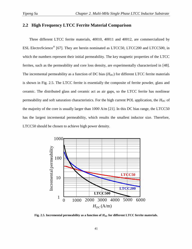
Yipeng Su Chapter 2. Multi-MHz Single Phase LTCC Inductor Substrate
41
2.2 High Frequency LTCC Ferrite Material Comparison
Three different LTCC ferrite materials, 40010, 40011 and 40012, are commercialized by
ESL ElectroScience® [67]. They are herein nominated as LTCC50, LTCC200 and LTCC500, in
which the numbers represent their initial permeability. The key magnetic properties of the LTCC
ferrites, such as the permeability and core loss density, are experimentally characterized in [48].
The incremental permeability as a function of DC bias (HDC) for different LTCC ferrite materials
is shown in Fig. 2.5. The LTCC ferrite is essentially the composite of ferrite powder, glass and
ceramic. The distributed glass and ceramic act as air gaps, so the LTCC ferrite has nonlinear
permeability and soft saturation characteristics. For the high current POL application, the HDC of
the majority of the core is usually larger than 1000 A/m [21]. In this DC bias range, the LTCC50
has the largest incremental permeability, which results the smallest inductor size. Therefore,
LTCC50 should be chosen to achieve high power density.
Fig. 2.5. Incremental permeability as a function of HDC for different LTCC ferrite materials.
0 1000 2000 3000 4000 5000 60001
10
100
1000
LTCC500
LTCC200
LTCC50
HDC (A/m)
Incr
emen
tal p
erm
eabil
ity

Yipeng Su Chapter 2. Multi-MHz Single Phase LTCC Inductor Substrate
42
Fig. 2.6. Core loss density comparison for different LTCC ferrite materials.
Core loss at high operating frequency is another criterion for material selection. The core
loss density of the LTCC ferrites is compared in Fig. 2.6. In the interested frequency range from
1MHz to 10MHz, the core loss density of LTCC50 is one to two orders of magnitude lower than
that of LTCC200 and LTCC500 at the same AC flux excursion. As a benchmark, the core loss
density of the commercial NiZn ferrite (4F1) [68] is also included in this comparison, which the
core loss density of LTCC50 is close to. In summary, the LTCC50 is selected as the core
material to design the multi-MHz inductor for the high current POL converter, due to its low loss
density at high frequency and high incremental permeability at large DC bias condition.
2.3 Single-Phase LTCC Inductor Substrate Design
As shown in Fig. 2.7 and Fig. 2.8, two different versions of active layer are developed with
GaN devices from EPC and IR [69] [70]. The EPC’s discrete devices are targeting at high
current level (15A-20A), but relatively lower frequency (1MHz-3MHz); while IR’s monolithic
solution is used for relatively lower current (10A-15A) and higher frequency (3MHz-5MHz).
0 2 4 6 8 12
100
10
110
1000
10000
Frequency (MHz)
Co
re lo
ss d
ensi
ty (W
/in
3)
LTCC500LTCC200
LTCC50
4F1 NiZn
Bp= 5mT

Yipeng Su Chapter 2. Multi-MHz Single Phase LTCC Inductor Substrate
43
Instead of placing the active components on the LTCC inductor substrate directly, either multi-
layer PCB or two-layer DBC board is used to build the active layer, in which one layer serves as
the ground plane and shield. Because of the shielding layer, the magnetic mutual coupling
between the inductor substrate and the active circuit is blocked and the parasitic inductance of
the high frequency loop of the Buck converter is minimized. The active layer design and shield
layer optimization are discussed in [69] [70]. It can be seen that all the other components except
the inductor, are placed on top of the active board, and the bottom of the board is kept empty and
flat to mount the inductor substrate.
(a) (b)
Fig. 2.7. The active layer of the high frequency POL module with EPC’s discrete GaN:
(a) top view; (b) bottom view [69].
(a) (b)
Fig. 2.8. The active layer of the high frequency POL module with IR’s monolithic GaN:
(a) top view; (b) bottom view [70].

Yipeng Su Chapter 2. Multi-MHz Single Phase LTCC Inductor Substrate
44
This section studies the LTCC inductor substrates design for these high frequency POL
boards. 12V input voltage to 1.2V output voltage with 15A full load current and the switching
frequency range from 1MHz to 10MHz are used as the design examples. In order maximized the
power density of the POL module, the footprint of the inductor should be equal to that of the
active circuit. Therefore, the footprint of the inductor is assumed to be pre-determined by the
active layer in the design process.
(a) (b)
Fig. 2.9. Lateral flux LTCC inductor substrate with dimensional parameters to be designed:
(a) 3D view of the single-turn structure; (b) top view of multi-turn structure.
Fig. 2.10. DC flux distribution in single-turn LTCC inductor substrate with 15A DC input current.
The structures of the lateral flux LTCC inductor substrate have been shown in Fig. 1.29. The
blue vias embedded in the core are made of silver paste, which can be co-fired with LTCC ferrite.
2rv2g
gh
… … N
2rv
d
g2g
4g + 4rv
2g
+ 2
Nr v
+ (
N-1
)d

Yipeng Su Chapter 2. Multi-MHz Single Phase LTCC Inductor Substrate
45
The vias are connected with each other through the copper trace on the top and the bottom of the
core. The structure of the LTCC inductor substrate is controlled by three dimensional parameters,
which are the via size (rv), the core size (g) and the core thickness (h). They are illustrated in Fig.
2.9 with the 3D view of single-turn inductor and the top view of N-turn inductor. The d is
defined as the distance between two adjacent turns. The two adjacent turns should be placed as
close as possible to strengthen the mutual coupling [21]. The d value is fixed as 0.4mm, which is
the minimal value within our fabrication capability. In the basic design philosophy, the size of
the via is determined by the maximum output DC current, the size of the core is mainly
determined by the footprint of the inductor and the core thickness is designed to achieve the
desired inductance value.
Fig. 2.10 shows the flux distribution in the LTCC core with 15A DC current flowing
through the inductor. It can be seen that the flux distribution in the core is very non-uniform. The
core close to the vias is excited under large DC bias, while the DC bias of the core far away from
the vias is much smaller. Due to the nonlinear BH curve of the LTCC ferrite, the flux density and
the permeability at different part of the core both are different. The inductance and core loss
models for this planar LTCC inductor substrate with non-uniform flux distribution are proposed
in [62] and [63]. The basic concept is the core should be divided into a series of concentric rings,
and the flux and permeability in each ring is assumed to be constant. Therefore, the inductance
and core loss for each thin ring can be modeled individually with conventional approaches. The
total inductance and core loss of the inductor are the summation of the inductance and core loss
of each thin ring. The winding DC resistance loss can be calculated according to the dimension
of the winding structure. The winding AC resistance loss is analytically modeled in [71]
employing the FEA simulation.

Yipeng Su Chapter 2. Multi-MHz Single Phase LTCC Inductor Substrate
46
2.3.1 Design the dimensions of the LTCC inductor.
The desired inductance value for different frequency is first calculated according to the
circuit condition in (2.1), where Vin=12V and Vout=1.2V and the duty cycle D=0.1. The peak-to-
peak current ripple, ΔIpp, is chosen as 9A which is equal to 60% of DC output current at full load
(IDC=15A).
DfI
VVL
spp
outin
(2.1)
dNNrgrg vv 12244footprint (2.2)
dr
rrrdn
rn
hHnL
g
vv
nNDCr
nN
0
2
2
_
2
2
12
2
(2.3)
The via size, rv, is first calculated according to the output DC current at full load. The
maximum current density in the via is set as 15A/mm2 to limit the temperature rising. So the
radius of the via is chosen as rv=0.6mm to handle IDC(max)=15A. The footprint for N-turn LTCC
inductor is calculated by (2.2), in which d is minimized as 0.4mm. With rv=0.6mm, d=0.4mm and
footprint=141mm2 given by active circuit, the core size (gN) for different number of turns (N) can
be calculated as g1=3.6mm, g2=3.2mm, g3=2.9mm and g4=2.6mm. The core size is becoming
smaller for larger number of turns, due to more vias are needed.
The inductance analytical model for this lateral flux inductor substrate with non-uniform
flux and permeability distribution has been proposed and validated in [62]. The inductance can

Yipeng Su Chapter 2. Multi-MHz Single Phase LTCC Inductor Substrate
47
be calculated based on the dimensional parameters of the inductor with (2.3), which indicates
that for an N-turns LTCC inductor, the inductance is directly proportional to the core thickness
(h), if IDC, rv, d and g have been fixed.
The core thickness as a function of frequency for different N is compared in Fig. 2.11, with
which the desired inductance such as 60nH@2MHz, 30nH@4MHz and 20nH@6MHz can be
achieved. The core thickness larger than 3mm is out of our fabrication capability and not
considered. It can been seen that 1) the core thickness is continuously reduced with increasing
the frequency, because the required inductance is becoming smaller, and 2) core thickness also
can be reduced by increasing the number of turns. From 1-turn to 2-turn structure, there is
dramatic core thickness reduction, while the core thickness is reduced very little if N is increased
from three to four. For the inductor fabrication, multi-layer LTCC green tapes are laminated to
achieve the required core thickness. Therefore, the secondary vertical axis of Fig. 2.11 is marked
as the number of LTCC tape layers, which is directly proportional to the core thickness.
Fig. 2.11. Core thickness as a function of frequency for different number of turns.
Frequency (MHz)2 4 6 8 10
0
1
2
3
10
20
40
Lay
er No
. of G
reen T
ape
60
Co
re t
hic
kn
ess,
h(m
m)
N=4
N=3
N=2 N=1
Footprint=141mm2
rv=0.6mm
IDC=15A

Yipeng Su Chapter 2. Multi-MHz Single Phase LTCC Inductor Substrate
48
2.3.2 Inductor loss calculation
After the dimensional parameters of the LTCC inductor have been fixed, the inductor loss
can be evaluated for different switching frequency. The DC resistance (DCR) loss is first
calculated according to the dimension and properties of the winding structure. The vias are built
with DuPont®’s silver paste 7740, whose electrical conductivity is characterized to be
mS /1076.4 7 [47]. The copper sheet with 0.3mm thickness is used to connect the vias. Fig.
2.12 shows the winding DCR loss, which is continuously decreased as the frequency is increased,
because the smaller core thickness reduces the length of the silver vias. The AC resistance (ACR)
loss of the winding is plotted as Fig. 2.13, with the analytical model introduced in [71]. The ACR
loss of single-turn inductor keeps almost constant for different frequency. While the ACR loss of
multi-turn inductor rises quickly as frequency is increased due to the proximity effect, especially
when N is larger. From Fig. 2.12 and Fig. 2.13, it can be seen that both DCR and ACR losses are
sacrificed when N is increased.
Fig. 2.12. Winding DCR loss as a function of frequency for different number of turns.
2 4 6 8 100
0.2
0.4
0.6
1Frequency (MHz)
Win
din
g D
CR
loss
(W
)
N=1
N=4
N=3
N=2

Yipeng Su Chapter 2. Multi-MHz Single Phase LTCC Inductor Substrate
49
Fig. 2.13. Winding ACR loss as a function of frequency for different number of turns.
Fig. 2.14. Core loss as a function of frequency for different number of turns.
The analytical core loss model proposed in [63] is used to analyze the core loss of the LTCC
inductors. By utilizing the Modify Steinmetz's Equation (MSE) [72], this model considers the
impact of triangular flux waveform on the core loss, which is introduced by the triangular output
N=1
2 4 6 8 100
0.05
0.10
0.15
1
Frequency (MHz)
Win
din
g A
CR
loss
(W
)
N=4
N=3
N=2
2 4 6 8 100
0.1
0.2
0.3
1Frequency (MHz)
Co
re L
oss
(W
)
N=4N=3N=2
N=1

Yipeng Su Chapter 2. Multi-MHz Single Phase LTCC Inductor Substrate
50
current waveform of the Buck converter. The DC bias impact is also included, based on the core
loss density measured data under different DC bias condition [48]. Fig. 2.14 shows the core loss
is continuously increased as the frequency is increased, and the core loss difference for different
N is not as prominent as the winding loss.
Fig. 2.15. Inductor total loss as a function of frequency for different number of turns.
The comparison between winding loss and core loss indicates that the winding loss is still
the dominate part of the inductor loss for this low voltage, high current POL application. Fig.
2.15 shows the total inductor loss, which is derived as the summation of winding loss and core
loss. It is interesting to find that for a given N, the inductor loss does not change a lot in the
discussed frequency range. Since the winding DCR loss is decreased while the winding ACR
loss and core loss are increased as the frequency is increased, that almost stabilizes the inductor
total loss for different operating frequency.
2.3.3 Choosing the number of turns (N)
Frequency (MHz)
Ind
uct
or
loss
(W)
2 4 6 8 100
0.2
0.4
0.6
0.8
1
N=4
N=3
N=2
N=1

Yipeng Su Chapter 2. Multi-MHz Single Phase LTCC Inductor Substrate
51
From Fig. 2.11 and Fig. 2.15, it can be seen that choosing number of turns is essentially a
trade of between the core thickness and inductor loss, namely the power density and efficiency.
Increasing number of turns can always reduce the core thickness to achieve higher power density.
However, the inductor loss is increased and the efficiency is sacrificed. The other finding is that
the incremental inductor loss for different N is almost the same, which is roughly equal to 0.5%
output power (≈100mW).
Table 2.1. No. of LTCC Tape Layers for Different N at Different Switching Frequency
1MHz 2MHz 3MHz 5MHz 8MHz 10MHz
N=1 160 80 52 31 20 16
N=2 75 35 24 14 9 7
N=3 48 24 16 10 6 5
N=4 40 20 14 8 5 4
The numbers of LTCC tape layers to build the inductor for different frequency are list in
Table 2.1. Although single turn structure has the lowest loss, it would not be used, because too
many layers are needed to build the thick core. The 4-turn structure is also excluded, because
there is only very little layers reduction if N is increased from three to four. For the relatively
low frequency range from 1MHz to 3MHz, 3-turn structure is chosen to save tens layers of
LTCC tape, only paying the price of half percent output power. For the relatively high frequency
range from 4MHz to 8MHz, 2-turns structure is preferred. Because moving from 2-turn to 3-turn
only results several layers reduction and still suffers half percent output power.
Therefore, the 3-turn and 2-turn LTCC inductor substrates are employed for the POL
module with EPC’s GaN and the module IR’s GaN respectively, according to their different
optimal operating frequencies. It is found that the very simple single-turn structure would
become reality if the POL converter can be operated efficiently at 10MHz. By operated at higher

Yipeng Su Chapter 2. Multi-MHz Single Phase LTCC Inductor Substrate
52
frequency, not only the size of the inductor is shrunk to improve the power density of the module,
but also the inductor structure is simplified and the inductor losses is decreased. It is projected
the lateral flux unit cell shown in Fig. 1.25 (b) also can be used as the inductor substrate for the
3D integrated POL module, if the frequency is high enough in the near future. The winding loss
is minimized in this structure, since the surface winding is not required anymore. The fabrication
processes of the low profile inductor substrate also becomes very easy and simple.
2.4 Fabrication and Evaluation of the LTCC inductor Substrates
The high frequency POL converter built with EPC’s GaN devices is optimized for 1MHz to
3MHz, in which the 3-turn LTCC inductor is preferred. The LTCC inductors working at 1MHz,
2MHz and 3MHz are fabricated as shown in Fig. 2.16, following the same process in [21]. The
footprints are kept as the same as the active circuit, the only difference is the variation of the core
thickness. The copper traces are soldered on the top and bottom of the LTCC inductor to connect
the vias, as shown in Fig. 2.17.
Fig. 2.16. 3-turn LTCC inductor substrates working at 1MHz, 2MHz and 3MHz.

Yipeng Su Chapter 2. Multi-MHz Single Phase LTCC Inductor Substrate
53
(a) (b)
Fig. 2.17. 3-turns LTCC inductor substrate with surface winding: (a) top view, (b) bottom view.
Fig. 2.18. The inductance of the LTCC inductors at different DC current.
The inductance with different DC current is first tested in the evaluation procedure. The
LTCC inductors work as the output inductor of a Buck converter. With different output current,
the inductance can be measured as the ratio of the voltage second on the inductor to the peak-to-
peak current ripple. The dot points in Fig. 2.18 are the measured inductance with different DC
bias current and the inductance curves are predicted by the analytical model in [62]. The results
from measurement and calculation match very well, which validates of the inductance analytical
model again. The other observation is the nonlinear inductance of the LTCC inductor. Because
of the nonlinear permeability of the LTCC ferrite, the LTCC inductance becomes larger as the
DC current is decreased. The light load efficiency of the POL converter can be improved due to
the smaller current ripple of the inductor.
DC Current (A)
Ind
uct
ance
(n
H)
0 5 10 15 200
100
200
300
400
1#
2#
3#

Yipeng Su Chapter 2. Multi-MHz Single Phase LTCC Inductor Substrate
54
The LTCC inductors are soldered on the backside of the active circuit to realize the low
profile 3D integrated POL module as shown in Fig. 2.19 (a). Besides tested with LTCC inductor
substrates, the converter efficiency is also measured with some discrete inductors from
Coilcraft®. The discrete inductors, which have the approximative inductance as the LTCC
counterparts at full load condition, are chosen. The detailed comparison for different inductors is
list in Table 2.2. Different from the LTCC inductors, the discrete inductors use single turn and its
winding resistance is much smaller. The conventional design with large air gap for the discrete
inductor results constant inductance for different DC bias condition. The thickness for each
discrete inductor is around 5mm, which is much larger than its LTCC counterpart. The tested
POL module with discrete inductor is illustrated in Fig. 2.19 (b).
(a) (b)
Fig. 2.19. High frequency POL module with different inductors:
(a) POL module with LTCC inductor, (b) POL module with discrete inductor.
Table 2.2. Comparison between Discrete Inductors and LTCC Inductors
1MHz 2MHz 3MHz
LTCC 1# SLC1049-
121ML LTCC 2#
SLC1049-
750ML LTCC 3#
SLC7649S-
360KLB
L@15A 120nH 121nH 60nH 75nH 40nH 36nH
DCR 1.3mΩ 0.3mΩ 1.2mΩ 0.3mΩ 1.1mΩ 0.2mΩ
h 2.4mm 5.1mm 1.2mm 5.1mm 0.8mm 5.0mm
GaNDriver
LTCC inductor substrate
Discrete inductor

Yipeng Su Chapter 2. Multi-MHz Single Phase LTCC Inductor Substrate
55
Fig. 2.20. Measured converter efficiency of the POL module with EPC’s GaN devices.
The measured converter efficiency with different inductors is shown in Fig. 2.20. It can be
seen that the efficiency of the POL with LTCC inductor is comparable with that of POL with
discrete inductor at 15A. The full load converter efficiency with discrete inductor is slightly
higher at 2MHz, due to a little bit larger inductance is used. Although the LTCC inductor has
higher winding loss, the smaller core volume and low core loss density of the LTCC ferrite
decrease the core loss and thus equalizes the inductor total loss. At light load condition, the
larger inductance of the LTCC inductor reduces the AC current ripple. Therefore, not only the
switching loss and conduction loss of the switches are decreased, but also the inductor ACR
winding loss is reduced. The light load efficiency of the converter can be significantly improved
by the nonlinear inductance of the LTCC inductor.
0.76
0.78
0.80
0.82
0.84
0.86
0.88
0.90
0.92
0 5 10 15 20
Discrete Inductor
LTCC Inductor
12V Vin
1.2V Vout
Output Current (A)
Eff
icie
ncy
1 MHz
2 MHz
3 MHz
Yipeng Su Chapter 2. Multi-MHz Single Phase LTCC Inductor Substrate
56
Following the same procedure, the 3D integrated POL module with IR’s GaN devices and 2-
turn LTCC inductor are designed and fabricated in Fig. 2.21. Its efficiency at 3MHz, 4MHz and
5MHz are measured and shown in Fig. 2.22, from which it can be seen the POL module can
achieve higher than 86% efficiency even at 5MHz operating frequency.
(a) (b) (c)
Fig. 2.21. 3D integrated POL module with IR’s GaN devices and 2-turn LTCC inductor substrate:
(a) top view of 2-turn LTCC inductor; (b) bottom view of 2-turn LTCC inductor; (c) integrated POL module.
Fig. 2.22. Measured converter efficiency of the POL module with IR’s GaN and 2-turn LTCC inductor.
12 Vin , 1.2 Vout
3 MHz
5 MHz
4 MHz
Output Current (A)
Eff
icie
ncy
0.80
0.82
0.84
0.86
0.88
0.90
0.92
0 2 4 6 8 10 12

Yipeng Su Chapter 2. Multi-MHz Single Phase LTCC Inductor Substrate
57
The power density of the POL module with LTCC inductor and discrete inductor is
compared in Fig. 2.23. Due to the ultra-low profile design and fully utilization of the space, the
LTCC inductor can improve the power density prominently. Moreover, the power density
improvement becomes significant at higher frequency. Since the thickness of the LTCC inductor
is continuously decreased with increasing frequency. However, the thickness of discrete inductor
keeps almost unchanged. The power density of the 3D integrated POL module with EPC’s GaN
device is as high as 700W/in3 at 2MHz and 800W/in
3 at 3MHz. Because of the higher frequency
and shrinking footprint, the power density of the POL module with IR’s GaN device achieves as
high as 900W/in3 at 5MHz and 10A output current, even if 2-turn structure is used.
Fig. 2.23. Comparison of the high frequency POL module with different inductor structures.
300
500
700
900
1100
0 1 2 3 4 5 6
LTCC inductor
Discrete inductor
Frequency (MHz)
Po
wer
Den
sity
(W
/in
3)
15A Iout
12V Vin
1.2V Vout
POL with
IR’s GaN
POL with
EPC’s GaN

Yipeng Su Chapter 2. Multi-MHz Single Phase LTCC Inductor Substrate
58
2.5 Summary
This chapter discusses the lateral flux LTCC inductor substrate design for multi-MHz 3D
integrated POL module. The impact of high frequency on the inductor design is analyzed. Based
on the trade of between core thickness and inductor loss, 3-turns inductor is used for POL
module with EPC’s GaN devices, which is operated from 1MHz to 3MHz. The 2-turns inductor
is preferred for the POL module with IR’s GaN devices running from 3MHz to 5MHz. The high
frequency operation can reduce the number of LTCC tape layer to build the inductor substrate,
and the number of turns of the inductor. The fabrication process of the inductor can be simplified
and the inductor cost is also decreased. The LTCC inductor substrates working at different
frequency are fabricated and tested on the high frequency POL converter. The measured
efficiency and power density of the module with LTCC inductors are compared with that with
some commercial discrete inductors. It is experimentally demonstrated several benefits of the
LTCC inductor, such as light load efficiency improvement, high power density and capability of
integration. The 12V to 1.2V, 10A-15A integrated POL modules with LTCC inductor substrate
achieve more than 85% efficiency and 800W/in3 power density at multi-MHz operating
frequency.

Yipeng Su Chapter 3. FEA Modeling of the Lateral Flux Coupled Inductor
59
Chapter 3.
FEA Modeling of the Lateral Flux Coupled Inductor
Using IR’s GaN devices and the single-phase LTCC inductor substrates, a 5MHz, 10A POL
module has been demonstrated as 900W/in3 power density in last chapter, which is roughly 2-3
times of the power density of the state-of-the-art alternatives with same current level. The 20A
output current can be easily achieved by paralleling two-phase converters. For the two-phase
POL converter with GaN designed in [70], either two single-phase inductors or one two-phase
coupled inductor can be used as the magnetic substrate. The coupled LTCC inductor substrate
has been proposed in [21] for the two-phase POL converter. The DC flux cancellation effect
reduces the footprint of the inductor substrate by 52%, without suffering any core thickness.
From the electrical point of view, the inverse coupled inductor improves the transient speed of
the converter while maintains small steady state current ripple [64]. However, the impact of the
inversed coupling on the magnetic performance of the inductor is unclear. In order to study this
problem, the Finite Element Analysis (FEA) simulation models to calculate the inductance and
core loss of the lateral flux coupled inductor are established in this chapter. With the help of FEA
models, the coupled inductor substrates are designed and evaluated for multi-MHz two-phase 3D
integrated POL modules. The analysis reveals the several benefits of the inverse coupling, which
are desirable especially for high current POL application.
3.1 Challenges to Model the Lateral Flux Coupled Inductor
The conceptual drawing of the two-phase coupled inductor with N=2, is illustrated in Fig.
3.1. The coupled inductor is actually constructed by embedding two windings in one core, so that

Yipeng Su Chapter 3. FEA Modeling of the Lateral Flux Coupled Inductor
60
flux from different inductors is magnetically coupled. With the marked current direction, the
inverse coupling between the two inductors is realized, which means the flux created by different
inductors are in opposite direction.
Fig. 3.1. Lateral flux inverse coupled inductor substrate with N=2.
(a) (b)
Fig. 3.2. Field distribution in a lateral flux coupled inductor with 10A DC current in each phase (top view):
(a) DC magnetic intensity (HDC); (b) Incremental permeability
Excited by 10A DC current in each phase, the DC magnetic intensity (HDC) in the core of
coupled inductor is shown in Fig. 3.2 (a). It can be seen the flux distribution in the core is very
non-uniform. This problem becomes even more complicated when the planar core is built using
the LTCC ferrite material with nonlinear permeability. Fig. 3.2 (b) shows the non-uniform
distributed permeability in the coupled inductor when the core is built with LTCC ferrite 40010
from ESL®. The core with higher DC bias has low permeability and high reluctance. Moreover,
2g
g
dL
hiL1
iL2
HDC (A/m) r

Yipeng Su Chapter 3. FEA Modeling of the Lateral Flux Coupled Inductor
61
the lateral flux coupled inductor has non-uniform distributed core loss density, which is usually
the function of flux. Therefore, the conventional reluctance model and core loss model assuming
uniform flux are not able to predict the inductance and core loss of the coupled inductor precisely.
The analytical models to calculate the inductance and core loss of the single-phase lateral flux
inductor with non-uniform flux distribution have been proposed and validated in [62] and [63],
in which the core is represented by a series of concentric rings. Each small ring assumed to have
constant flux is modeled by conventional methods. This approach however is not suitable for the
coupled inductor, in which the flux distribution becomes even irregular and coupling dependent.
Fig. 3.3. Fundamental principle of FEA simulation to model the magnetic core with non-uniform flux.
In industry and academia, computer aided tools have become more and more involved in the
design of magnetic components. The FEA method is one of the most popular numerical
techniques for solving electromagnetic problems. As illustrated in Fig. 3.3, the basic principle of
FEA simulation is to split the entire core into some small pieces (i.e. elements), in which the flux
#1
#2
#3

Yipeng Su Chapter 3. FEA Modeling of the Lateral Flux Coupled Inductor
62
can be assumed constant, so that the modeling of the small elements can be followed as the
conventional ways. The total flux and core loss are the summation of that of every small element.
The accuracy of this numerical technique has been established and validated. The numerical
inductance model is proposed for the single-phase inductor with non-uniform flux, and its
accuracy has been verified by measurement in [63]. In the following section, the FEA simulation
is extended to cover the inductance as well as the core loss modeling for the two-phase coupled
inductor.
3.2 Inductance Modeling
iLAC
(3.1)
For POL applications, the inductance value needs to represent the ac energy excursion,
which can be used to predict the inductor current ripple. Therefore, the AC inductance defined as
the ratio between incremental flux and incremental current in (3.1) is desired. In addition, the DC
bias operating point should be taken into account. Due to the nonlinear B-H curve of LTCC
ferrites, the relation between the exciting current and the total flux coupled with the current in
the LTCC inductor becomes nonlinear [21], as shown in Fig. 3.4. The target is essentially
calculating the slope of the Ψ-i curve at given DC operating point.
For the AC flux calculation, it is better to use the eddy current solver to simulate the LTCC
inductor. However, the MaxwellTM
eddy current solver is not able to define the material with
nonlinear B-H curve, and the operating point is always at origin of the B-H curve. The magneto
static solver can support material with nonlinear B-H curve, and the DC operating point can be
arbitrarily chosen. Unfortunately, the magneto static solver only calculates the DC flux according

Yipeng Su Chapter 3. FEA Modeling of the Lateral Flux Coupled Inductor
63
to the DC excitation. Therefore, two-step magneto static simulations are used to calculate the AC
flux at given DC operating point as shown in Fig. 3.4. The incremental current between the
excitations of the two magneto static simulations is defined as Δi, and ΔΨ represents the
difference of the flux coupled with the exciting current between the two magneto static
simulations. If Δi is smaller enough, the ratio of ΔΨ to Δi can be derived as the slope of the Ψ-i
curve at a given DC operating point.
Fig. 3.4. Nonlinear relationship between the exciting current and total flux
coupled with excitation for the LTCC inductor.
Specifically for the lateral flux coupled inductor, the 3D FEA simulation model is
constructed in Ansoft® Maxwell
TM as shown in Fig. 3.5. In the first step, two identical DC
excitations, IDC, are applied into L1 and L2, as shown in Fig. 3.5 (a). The magneto static solver
calculates the DC flux designated as Ψ1 and Ψ 2, which are the DC flux linked with i1 and i2. In
Ψ
i
Ψ1
Ψ1’
IDC+∆iIDC

Yipeng Su Chapter 3. FEA Modeling of the Lateral Flux Coupled Inductor
64
the second step, a small incremental current, ∆i, is injected into L1. The DC current in L1
becomes IDC+∆i, while the DC current in L2 maintains as IDC, as shown in Fig. 3.5 (b). Then the
DC flux linking with i1' and i2' can be obtained as Ψ1' and Ψ2'. The self-inductance of L1 and the
mutual inductance between L1 and L2 at operating point IDC can be calculated with (3.2) and (3.3).
L1 and L2 should have identical self-inductance, because of the symmetrical structure. Based on
the basic theory of coupled inductor [64], the equivalent steady state inductance (Lss) and the
equivalent transient inductance (Ltr) can be calculated as (3.4) and (3.5). They are the function of
self-inductance (Lself), mutual coupling (α) and the duty cycle (D) of the POL converter.
(a) (b)
Fig. 3.5. Two steps of magneto static simulation to calculate the AC flux at a given DC operating point:
(a) step one; (b) step two
iLself
11 '
(3.2)
iM
22 '
(3.3)
L1
L2
L1
L2

Yipeng Su Chapter 3. FEA Modeling of the Lateral Flux Coupled Inductor
65
D
DL
MD
DL
MLL self
self
self
ss
11
1
1
222
(3.4)
1selfselftr LMLL (3.5)
Three parameters can be controlled to achieve different structure of the coupled inductor.
They are the size of LTCC core, g, the thickness of LTCC core, h, and the distance between two
inductors, dL, as labeled in Fig. 3.1. With the inductance model, the impact of these parameters
on the inductance of the coupled inductor is discussed. The study is based on a two-phase POL
converter working at Vin=12V, Vout=1.2V, Iout=10A in each phase and fs=2-10MHz [70]. In this
frequency range, the LTCC ferrite 40010 is chosen as the core material.
To achieve high power density and high efficiency, the steady state inductance (Lss) is
maximized with a given core volume in the design process. Similar as the single-phase LTCC
inductor, the design of the coupled inductor is also discussed with a predetermined footprint by
the active layer in [70]. Essentially, dL can be used to control the mutual coupling, h is varied to
achieve the required Lss for different operating frequency, g is chosen to fit the footprint of the
active layer (150 mm2).
First, the relationship between dL and the mutual coupling is examined. Fig. 3.6 shows the
mutual coupling as a function of dL when h=0.6mm, h=1.0mm and h=1.4mm, from which it can
be seen that for a given core thickness, the inversed mutual coupling can be enhanced by moving
two inductor closer. For the same dL value, the coupling becomes weaker when the core
thickness is reduced. That is mainly because the leakage flux created by the surface winding
becomes a more dominant part of the total flux when the core thickness is smaller.

Yipeng Su Chapter 3. FEA Modeling of the Lateral Flux Coupled Inductor
66
Fig. 3.6. Mutual coupling as a function of dL for different core thickness.
Fig. 3.7. Steady state inductance as a function of dL for different core thickness.
Then the core thickness is arbitrarily chosen as h=0.8mm, 1.0mm and 1.2mm, dL is swept
from 0.4mm (minimal value within our fabrication capability) to 2.8mm. As dL is increased, the
core size (g) is continuously decreased to keep the footprint constant. The variation of steady
0
0.2
0.4
0.6
0.8
0 0.5 1 1.5 2 2.5 3
h=0.4mm
h=1.0mm
h=1.6mm
dL (mm)
35
45
55
65
0 0.5 1 1.5 2 2.5 3
h=0.8mmh=1.0mmh=1.2mm
dL (mm)
Lss
(nH)
|α|=0.3
|α|=0.3
|α|=0.3

Yipeng Su Chapter 3. FEA Modeling of the Lateral Flux Coupled Inductor
67
state inductance with dL is obtained from FEA simulation, as shown in Fig. 3.7. It can be seen the
Lss is maximized when |α| is equal to 0.3. At the same time, dL should be decreased when h is
reduced to keep the optimal coupling. For any core thickness, the footprint is kept the same when
dL is changed, so the core volume is constant value. The steady state inductance can be optimized
for a given core volume.
The reason for the optimal Lss can be explained by reexamining equation (3.4). The steady
state inductance is expressed as the product of two parts. The first part is the self-inductance (Lself)
and the second part is only the function of coupling if D is equal to 0.1 for this 12V to 1.2V POL
converter. The relationship between Lself and coupling is further explained by Fig. 3.8 and Fig.
3.9. Fig. 3.8 (a) shows the DC flux distribution of a single-phase non-coupled inductor with 10A
DC bias current. It can be seen that the HDC value of the majority of the core is very large. Using
the typical area in the center of the core marked by black dot as the example, its operating point
is at DC bias higher than 2000A/m, which is associated with the B-H curve of LTCC ferrite in
Fig. 3.9. If two single-phase inductors are inversed coupled together with 0.3 coupling
coefficient and the DC bias current in each phase is still kept as 10A, the DC operating point of
the core at the same marked point can be reduced to around 1000A/m, as shown in Fig. 3.8 (b).
The coupling is enhanced by decreasing the distance between two inductors (i.e. dL). It is
illustrated in Fig. 3.8 (c) the coupling coefficient is increased to 0.5 with dL=0.4mm, which
results the DC operating point of the core at the black dot point is reduced to several hundred
A/m. In Fig. 3.8, the solid line is the direction of the inductor current and the dash line represents
the flux line in the core. Because of the nonlinear B-H curve of the LTCC ferrite 40010 as shown
in Fig. 3.9, the incremental permeability is continuously increased as the coupling is enhanced,
namely DC bias in the core is decreased.

Yipeng Su Chapter 3. FEA Modeling of the Lateral Flux Coupled Inductor
68
(a)
(b)
(c)
Fig. 3.8. DC flux distribution of the lateral flux LTCC inductor with 10A current in each phase: (a) non-
coupled; (b) inverse coupled with |𝜶| = 𝟎. 𝟑 and dL=1.6 mm; (c)inverse coupled with |𝜶| = 𝟎. 𝟓 and dL=0.4 mm.
Fig. 3.9. DC operating points and permeability for inductors with different coupling coefficients.
HDC (A/m)
dL =1.8 mm
35.0
6.0
dL =0.4mm
0
10
20
30
40
50
0 1000 2000 3000 4000 5000
HDC (A/m)
r
Δμr_a
Δμr_b
Δμr_c
Δμr_c > Δμr_b > Δμr_a

Yipeng Su Chapter 3. FEA Modeling of the Lateral Flux Coupled Inductor
69
The stronger inversed mutual coupling (i.e. smaller dL value) means more DC flux in the
core is cancelled and larger permeability of the LTCC material. Therefore, the first part in (3.3),
Lself, is always increased if the mutual coupling is enhanced, while the second part is always
decreased. The product of these two parts leads to the “mountain-shape” Lss curve as shown in
Fig. 3.7. From the magnetic point of view, the mutual coupling should be neither too low nor too
high. If it is too low, the DC flux cancellation effect is not effectively utilized. If it is too high,
the coupled inductor acts as the transformer and the energy density stored in the magnetic core
becomes very low.
The same process is repeated with the variation of h, in order to find the optimal Lss for
different core thickness. It is interesting to find that the optimal Lss is always achieved when the
|α|=0.3 for this specific case with given footprint and DC current. When h is reduced, two
inductors should be moved closer accordingly to maintain the optimal coupling coefficient (i.e.
|α|=0.3). The curve for the optimal Lss is plotted in Fig. 3.10.
Fig. 3.10. The optimal steady state inductance for different core thickness.
0
20
40
60
80
100
120
0 0.5 1 1.5 2 2.5
h (mm)
Lss
(nH)

Yipeng Su Chapter 3. FEA Modeling of the Lateral Flux Coupled Inductor
70
Fig. 3.11. Core thickness comparison between inverse coupled and non-coupled inductors.
Fig. 3.12. Comparison between the power density of the POL modules
with inverse coupled and non-coupled inductors.
To make fair comparison between the one two-phase inverse coupled inductor and two non-
coupled inductors, both of them are designed for the POL converter to achieve the same steady
0
0.5
1
1.5
2
2.5
3
2 4 6 8 10
coupled L
non-coupled L
fs (MHz)
core
th
ick
nes
s, h
(mm
)
500
700
900
1100
1300
2 4 6 8 10
with coupled L
with non-coupled L
fs (MHz)
po
wer
den
sity
(W
/in
3)
150W/in3

Yipeng Su Chapter 3. FEA Modeling of the Lateral Flux Coupled Inductor
71
state current ripple. For different frequency, the peak-to-peak value of the steady state AC
current ripple is kept as 60% of full load DC current (10A). The required inductance is calculated
with (3.6) for different frequency. The footprint of the coupled inductor is set to be double of that
of the single-phase inductor, so the core thickness difference reflects the volume difference. The
LTCC core thickness of non-coupled and coupled inductor for different frequency is compared
in Fig. 3.11, from which it can be seen the core thickness is reduced by 40% using the inverse
coupled inductor structure due to the DC flux cancellation. Therefore, the power density of the
high frequency 3D integrated POL module is increased by 150W/in3, as shown in Fig. 3.12.
DfI
VVL
spp
outinss
(3.6)
3.3 Core Loss Modeling
In this section, the coupled inductor designed to work at 4MHz is used as an example to
analyze the impact of inverse coupling on the core loss. The key parameters of the coupled
inductor are compared with those of non-coupled inductor in Table 3.1. The inverse coupling
reduces core thickness from 1.4mm to 0.8mm, while maintains the footprint and the steady state
inductance. Fig. 3.13 shows the current waveform of the coupled inductor determined by both Lss
and Ltr, which is imported into Ansoft®
MaxwellTM
3D transient simulation as the excitations.
Table 3.1. Comparison between Inverse Coupled and Non-coupled Inductors for 4MHz applications
Lss Ltr footprint h dL
Inverse coupled Inductor 45 nH 33.7 nH 150 mm2 0.8 mm 1.6 mm
Non-coupled Inductor 45 nH 45 nH 2*75mm2 1.4 mm N/A

Yipeng Su Chapter 3. FEA Modeling of the Lateral Flux Coupled Inductor
72
Fig. 3.13. Current waveform of the coupled inductor imported into Maxwell transient simulation.
The non-uniform distributed flux in the lateral flux LTCC inductor substrate results non-
uniform distribution of the core loss density. So the traditional approach assuming uniform core
loss density cannot be used any more. In the finite element analysis, the core is divided into a
series of small elements as shown in Fig. 3.3. The DC and AC flux, as well as the core loss
density, in each small element is regarded to be constant. Therefore, the core loss for each
element is calculated individually. The core loss of the entire core is the summation of that of
every element. As we know, the core loss density is not only related to DC bias, AC flux
excursion, but also the flux waveform [73]. In order to calculate the core loss density, the flux
waveforms in the finite elements are checked by using the Ansoft® Maxwell
TM 3D transient
simulation.
Fig. 3.14 shows the flux waveforms in three typical finite elements in the coupled inductor.
It is observed that (1) each element (different location of the core) has its own DC and AC flux,
which emphasizes the necessity of the FEA approach to calculate the core loss of this structure;
6
8
10
12
14
0 100 200 300 400 500
iL
(A)
t (ns)
iL1 iL2

Yipeng Su Chapter 3. FEA Modeling of the Lateral Flux Coupled Inductor
73
(2) the flux waveform in each element is very different; (3) The flux waveform in each element
is non-sinusoidal, some of them are even not triangular any more, such as elements #2 and #3.
Therefore, the core loss of each element should calculate according to its own AC flux excursion,
DC bias and the flux waveform.
Fig. 3.14. Flux waveforms in typical elements of the lateral flux coupled inductor.
0
20
40
60
80
0 100 200 300 400 500
B
(mT)
t (ns)
#3
#2
#1
#1
#2
#3

Yipeng Su Chapter 3. FEA Modeling of the Lateral Flux Coupled Inductor
74
Traditionally, the core loss density under sinusoidal excitation is calculated by the Original
Steinmetz Equation (OSE). Several empirical core loss evaluation methods for non-sinusoidal
flux waveform have been proposed, such as Modified Steinmetz Equation (MSE) [72],
Generalized Steinmetz Equation (GSE) [74], Improved Generalized Steinmetz Equation (IGSE)
[75], Natural Steinmetz Extension (NSE) [76] and Equivalent Elliptical Loop (EEL) [77]. All of
them try to make modifications of the OSE, so that the core loss density under non-sinusoidal
flux can be evaluated using only Steinmetz parameters provided by the manufacturer of the
magnetic materials.
The Equivalent Elliptical Loop (EEL) core loss model has been functionally embedded into
Ansoft® MaxwellTM
transient solver. Instead of deriving the core loss in frequency domain like
such as MSE, GSE, IGSE and NSE, the EEL model calculates the instantaneous core loss under
arbitrary flux waveform. Then the instantaneous core loss is averaged in one switching cycle. It
is interesting to find that IGSE, NSE and EEL actually come to the same result.
In addition, the effect of the DC bias on the core loss should be taken into account. A
function consisting of a constant (Kdc), DC flux (BDC) and AC flux (Bm), is added into EEL
model to take the DC offset of the magnetic field into consideration [78]. The equations for EEL
model are listed as (3.7) and (3.8), where (3.7) is the instantaneous core loss, only based on
Steinmetz parameters, k, α and β; (3.8) is the average of the instantaneous core loss including the
effect of DC bias. However, the limit of (3.8) is the weak flexibility of Kdc term. The Kdc term is
a monotonic function, which sometimes fails to model the core loss under different DC bias. For
some magnetic materials, the core loss density drops first and then increases again as DC bias is
increased, such as LTCC ferrite 40011 from ESL®
[48].

Yipeng Su Chapter 3. FEA Modeling of the Lateral Flux Coupled Inductor
75
dt
dBB
d
ktp mv
2
0cos
22
cos
(3.7)
T
vmDCdcv dttpT
BBKP0
11/ (3.8)
T
vDCv dttpT
HfP0
1 (3.9)
11069.8 4
DCDC HHf (3.10)
Fig. 3.15. Core loss density of LTCC40010 at different DC bias modeled by f(HDC).
Based on a bunch of measured core loss data under different DC bias, [79] proposes to
decouple the impact of DC bias on the core loss density from the AC flux. A polynomial term,
which is the only function of HDC is used to model the core loss density at different DC bias.
When the AC flux is changed, the HDC term is still kept as the same. Moreover, the polynomial
0 1000 2000 3000 400010
100
1000
10000
Pv
(kW
/m3)
HDC(A/m)
Bm=5mT
Bm=10mT
Bm=15mTLTCC 40010

Yipeng Su Chapter 3. FEA Modeling of the Lateral Flux Coupled Inductor
76
can be arbitrarily chosen according to the characteristics of the magnetic material, which give
much more flexibility for the core loss model to fit different materials.
Combining the modeling approach for the arbitrary waveform in EEL model and the
polynomial term to consider the DC bias impact in [79], a complete model as (3.7), (3.9) and
(3.10), to calculate core loss density of each small element under arbitrary flux with DC bias can
be derived. A linear equation in (3.10) is actually obtained by curve fitting the measured core
loss data of LTCC 40010 under different DC bias [48]. As shown in Fig. 3.15, the curves
predicted by (3.10) can match the measured data (dots) very well, even if at different AC flux
conditions.
The comparisons between DC and AC flux distributions of coupled inductor and non-
coupled inductors are illustrated in Fig. 3.16 and Fig. 3.17, respectively. The DC flux level is
decreased in the inverse coupled inductor due to the DC flux cancellation effect. For the LTCC
40010 ferrite material, the core loss density is increased linearly as the DC bias (HDC) is
increased, as indicated in (3.10). Therefore, the inverse coupling has the positive effect on the
core loss density reduction from the DC flux perspective.
For the inductor working in the POL converter, the total AC flux is clamped by the voltage-
second of the circuit. As long as the voltage-second is unchanged, the total AC flux in the LTCC
core is constant. The inverse coupling does not affect the AC flux density if the inductor volume
is not changed. However, the core thickness is decreased by the inversed coupling, because the
DC flux cancellation increases the permeability of the LTCC core. The smaller core thickness
results higher AC flux density, as shown in Fig. 3. 17. From the AC flux density point of view,
the inversed coupling has the negative effect on core loss density. The other observation is the

Yipeng Su Chapter 3. FEA Modeling of the Lateral Flux Coupled Inductor
77
AC fluxes density in the middle part of the coupled inductor is cancelled due to the phase-shift
interleaving between the two channels of the converter
(a) (b)
Fig. 3.16. DC flux comparison between non-coupled and invers coupled inductors for 4MHz POL:
(a) non-coupled, (b) inverse coupled.
(a) (b)
Fig. 3.17. AC flux comparison between non-coupled and invers coupled inductors for 4MHz POL:
(a) non-coupled, (b) inverse coupled.
Fig. 3.18 shows the core loss density distribution of the LTCC coupled and non-coupled
inductors, both working at 4MHz. The inversed coupling actually decreases the DC flux, but
increases the AC flux in the LTCC core, which has positive and negative effects on the reduction
h=1.4mm h=1.4mmh=0.8mm, dL=1.6mm
HDC (A/m)
h=1.4mmh=1.4mmh=0.8mm, dL=1.6mm
Bm (mT)

Yipeng Su Chapter 3. FEA Modeling of the Lateral Flux Coupled Inductor
78
of the core loss density, respectively. Therefore, these two effects balance each other and the
inversed coupling thus has very little impact on the core loss density. The total core losses are
calculated as Pcore = 220 mW for two non-coupled inductors and Pcore = 147 mW for one two-
phase inverse coupled inductor. Eventually, the inversed coupling reduces the inductor core loss
by more than 30%, due to the smaller core thickness of the coupled inductor (i.e. smaller core
volume).
(a) (b)
Fig. 3.18. Core loss density comparison between non-coupled and invers coupled inductors for 4MHz POL:
(a) non-coupled, (b) inverse coupled.
In summary, the inverse coupling can dramatically reduce the core thickness of the LTCC
inductor substrate, because the DC flux cancellation increases the permeability of the core
material. In addition, lower DC bias results smaller core loss density. However, the smaller core
thickness of the coupled inductor crowds the AC flux density and increases the core loss density.
The inversed coupling can still reduce the total core loss, which is mainly coming from the
shrink of the core volume.
3.4 Experimental Verification of the FEA Models
h=1.4mm h=1.4mmh=0.8mm, dL=1.6mm
Pv (W/m3)

Yipeng Su Chapter 3. FEA Modeling of the Lateral Flux Coupled Inductor
79
The LTCC coupled inductor working at 4MHz is fabricated as shown in Fig. 3.19 for the
testing and evaluation. The two-phase 3D integrated POL module built with IR’s GaN and
LTCC coupled inductor is shown in Fig. 3.20, whose power density achieves as high as
900W/in3. The equivalent steady state inductance of the coupled inductor is obtained by
measuring the steady state current ripple of the POL converter. The measured result and
simulated data match very well as shown in Fig. 3.21, which validate the inductance FEA model.
Fig. 3.19. Fabricated lateral flux coupled inductor substrate for 4 MHz POL module.
Fig. 3.20. Tow-phase 3D integrated POL module with IR’s GaN and LTCC coupled inductor substrate
(4MHz, 20A, 900W/in3).
LTCC coupled inductor substrate

Yipeng Su Chapter 3. FEA Modeling of the Lateral Flux Coupled Inductor
80
Fig. 3.21. Comparison of the measured and simulated steady state inductance.
From the converter efficiency comparison between the POL with the coupled inductor and
non-coupled inductor in Fig. 3.22, it can be seen that the inverse coupled LTCC inductor
improves the efficiency a little at full load condition. Since the steady state current ripple for
these two cases is kept the same, the switching loss and conduction loss of the converter can be
assumed no difference. The efficiency improvement only comes from the core loss reduction of
the coupled inductor. It also should be noticed that the utilization of the coupled inductor
increases the power density by 150W/in3. At the light load condition, the cores of coupled
inductor and non-coupled inductor are both excited under low DC bias, while the AC flux
density is the same as the full load condition. Without benefit from the DC flux reduction, the
coupled inductor at light load has much higher core loss density than that of non-coupled
inductor. Even if with smaller core volume, the coupled inductor has comparable core loss with
the non-coupled one. Therefore, the efficiency of POL with coupled inductor at light load.
30
40
50
60
70
80
0 2 4 6 8 10 12
Measured Lss
Simulated Lss
DC current in each phase (A)
Lss
(nH)

Yipeng Su Chapter 3. FEA Modeling of the Lateral Flux Coupled Inductor
81
Fig. 3.22. Efficiency comparison between the POL with inverse coupled and non-coupled inductors.
3.5 Summary
In order to design and analyze the two-phase inverse coupled inductor substrate for the 3D
integrated POL module, the FEA inductance and core loss models are developed in this chapter.
The incremental inductance is calculated through two-step magneto static simulations with small
perturbation; and the core loss is evaluated by the EEL core loss model with modified DC bias
term. With inversed coupling, the core volume can be reduced by 40%, since the DC flux
cancellation increases the permeability of the core material. In addition, lower DC bias leads to
the smaller core loss density. However, the smaller core thickness of the coupled inductor
crowds the AC flux density and increases the core loss density. These two effects balance each
other and keep the core loss density of the inverse coupled inductor at a similar level as that of
the non-coupled inductor. However, the inverse coupling can still reduce the core loss at full load
condition, which is mainly coming from the core volume shrink. The power density of the
0.82
0.84
0.86
0.88
0 2 4 6 8 10 12
w/ coupled inductor
w/ non-coupled inductors
Vin=12V, Vout=1.2V, fs=4MHz
Eff
icie
ncy
Output current (A)

Yipeng Su Chapter 3. FEA Modeling of the Lateral Flux Coupled Inductor
82
integrated POL module with LTCC coupled inductor can be pushed above 1kW/in3 at 5MHz,
which is around 5-8 times of the power density of state-of-the-art alternatives with the same
current level. Fig. 3.23 summarizes the power density achievement of the high frequency POL
module with EPC’s, IR’s GaN devices and LTCC inductor substrate, developed in chapter 2 and
chapter 3.
Fig. 3.23. Power density achievements of the POL modules with GaN devices and LTCC inductor substrates.
500
1A 20A10A
300
5A
100
40A
700
1000
Power
density
(W/in3)
15A Current30A
Power density is
calculated with 1.2Vout
The pictures are not
scaled to real size.
with IR’s GaN
with IR’s GaN
with EPC’s GaN

Yipeng Su Chapter 4. 3D Integrated POL Module with PCB Embedded Inductor Substrate
83
Chapter 4.
3D Integrated POL Module with PCB Embedded
Inductor Substrate
Using high frequency Gallium Nitride (GaN) devices and lateral flux LTCC inductor
substrates, the co-packaged POL modules operated at multi-megahertz and 10A-20A output
current, have been demonstrated with around 1kW/in3 power density in last two chapters.
However, this solution is not widely adopted by industrial products because of the relatively high
cost of the LTCC ferrite material. Secondly, the high temperature sintering (~900 ºC) of the
LTCC ferrite is still involved in the manufacturing process of the inductor, which further
increases the cost of the module. Finally, the GaN device is not mature enough to be used
extensively, and its cost is usually more than twice of the silicon alternatives in current stage.
The main target of this chapter is to explore a cost effective and low temperature integration
solution for the POL modules with high output current, which is ready to be commercialized
based on the state-of-the-art techniques
4.1 Review of the PCB Substrates with Embedded Core
Since most power converters of current design use printed circuit boards (PCBs) to support
the components, the technology of printed circuit board (including so-called multi-layer and
double-sided PCB) manufacture and electronic device populated on PCBs are both highly mature
technologies. Because the multi-layer PCBs are laminated structures, they can include embedded
components such as wiring. The magnetic core can also be embedded in a PCB structure without

Yipeng Su Chapter 4. 3D Integrated POL Module with PCB Embedded Inductor Substrate
84
requiring any process, which is incompatible with known production processes for conventional
PCBs. Moreover, when the magnetic core material is sandwiched between lamina of the PCB,
the windings for the magnetic components can be formed by the metal (e.g. copper) cladding
layers on both outer sides of the PCB or between PCB lamina, together with conventional vias
(also a very mature technology). The multi-layer PCBs with embedded magnetic layer for power
converter has been studied since the beginning of this century. The conceptual drawing of the
multi-layer PCB with embedded magnetic layer is illustrated in Fig. 4.1. This type of structure
essentially removes the footprint of the magnetic components from the total substrate area. The
total volume of the integrated power converter module is minimized by avoiding wasted space
between the magnetics and other components. The standardized process reduces the cost due to
less manual steps and no high temperature involved.
Fig. 4.1. Multi-layer PCB substrate with embedded layerwise magnetic core [45].

Yipeng Su Chapter 4. 3D Integrated POL Module with PCB Embedded Inductor Substrate
85
Following the laminating structure in Fig. 4.1, [45] designs and implements a 60W resonate
converter with PCB integrated transformer substrate as shown in Fig. 4.2 (a). The cross sectional
view of the embedded core and winding are shown in Fig. 4.2 (b). The soft magnetic layers (i.e.
MagLam) used in this prototype are made of ferrite polymer composite (FPC), which is cost
advantageous over the sintered ferrite and compatible to PCB manufacturing. However, the
higher losses and lower permeability of such material are issues for the high frequency operation.
(a) (b)
Fig. 4.2. Resonate DC-DC converter with PCB integrated transformer substrate [45]:
(a) prototype, (b) cross sectional view of the embedded magnetic layer and windings.
The magnetic alloy materials, such as NiFe, CoNiFe, have very high permeability and
saturation flux density. However, the thickness of the magnetic alloy has to be reduced below
20µm to minimize the high frequency eddy current loss, because of its low resistivity. The
magnetic foils can be laminated into the PCB carrier and then patterned by photolithography.
They can be treated just like copper layers. [60] presents a PCB integrated flyback transformer
for a 35 W PFC rectifier, in which tens of layers of commercialized alloy foils are stacked to
realize only 0.66mm core thickness. The electrical isolation is required between each layer. The
complicated laminating process makes the alloy foils unsuitable for the high current level POL

Yipeng Su Chapter 4. 3D Integrated POL Module with PCB Embedded Inductor Substrate
86
converter, where a large core volume is usually needed. The sintered MnZn ferrite with high
permeability, low core loss density and large enough core thickness also can be embedded into
PCB as the cores of power inductor and transformer[52] [61]. However, the shaping and
patterning the rigid ferrite involves special facilities, which is not easy to be handled. In addition,
the compatibility of the sintered ferrite with standard PCB manufacturing process is still
questionable.
The other approach using the magnetic alloy for high frequency applications is proposed by
a research team in University Delaware (UD) [43]. The Fe-based metal powder is milled into
flake shape with high aspect ratio (e.g. around 1μm thickness and 100μm lateral size). After
being coated with SiO2, the metal flake is bound with organic binder such as Polyethylene (PE)
or Polyvinyl Butyral (PVB). Then the composite can be either molded as magnetic core, or built
into thick-film form by tape casting. The thickness of the laminated thick-film structure can be
up to several mm. The metal flake composite can be cut and drilled with simple mechanical
machines due to its soft characteristic. Because of the high aspect ratio, the flake has to be
parallelly aligned with respect to the external magnetic field to minimize the eddy current loss.
The tape casting process has somewhat alignment effect on the flake, but not enough. On the
other hand, higher permeability and lower core loss density of the metal flake composite can be
achieved by increasing the volume ratio of the metal flake. Due to slightly misalignment and
relative low volume ratio (only 20%), the flake composite in [43] still has low permeability
(below 50) and high core loss density.
In the novel metal flake composite material developed by NEC/Tokin, both the alignment
and the volume ratio of the flake is improved. Although the detailed information about the
material, such as composition of the alloy, binding and insulating materials as well as the

Yipeng Su Chapter 4. 3D Integrated POL Module with PCB Embedded Inductor Substrate
87
aligning technique, is still confidential. The characterization of the NEC/Tokin’s material shows
the attractive magnetic performance. The relative permeability of this improved metal flake
composite is increased to several hundred, and its core loss density in multi-MHz range is
controlled to be comparable with that of the sintered NiZn ferrites. Therefore, NEC/Tokin’s
metal flake composite material is a good candidate to be embedded into PCB as magnetic core
for high current POL application. The compatibility of such flake core with conventional PCB
laminating process will be justified in next section.
4.2 PCB Embedded Core with NEC/Tokin’s Metal Flake Composite
The metal flake composite developed by NEC/Tokin is designated as SENFOLIAGE (SF).
The SF flake plates with different size and thickness are shown in Fig. 4.3. In the fabrication
process of the SF flake as illustrated in Fig. 4.4, the iron-based alloy powder is milled into
flattened flake, and then aligned in horizontal plane. After coated with oxide material and bound
with organic binder, the hot pressure is applied to combine the flattened flake as a sheet shape.
Finally, the flake plates are cured under temperature around 500ºC. The volume ratio of the alloy
flake is increased more than 50%, which is a significantly improved compared with the volume
ration of UD’s flake material reported in [43].
Fig. 4.3. SENFOLIAGE metal flake composite plates developed by NEC/Tokin.

Yipeng Su Chapter 4. 3D Integrated POL Module with PCB Embedded Inductor Substrate
88
Fig. 4.4. Aligning and binding processes for the SENFOLIAGE metal flake composite.
(a) (b)
Fig. 4.5. Cross section view of the microstructure for different metal flake composites
(a) material developed by University of Delaware [43], (b) material developed by NEC/Tokin [44].
Fig. 4.5 compares the internal microstructures of different metal flake composites from the
cross sectional view. It can be seen the alignment of the flake in NEC/Tokin’s material is much
better than that in UD’s material. The core loss density and permeability of SF flake are
measured with the setup in [79]. Fig 4.6 compares the core loss density data of SF flake, the
UD’s flake in [43], the electroplated CoNiFe thin film with 9.5µm thickness in [40] and the
LTCC50 ferrite. It can be seen that the SF flake has lower high frequency core loss density than
UD’s flake composite and CoNiFe thin film. The core loss density of SF flake is lower than
LTCC50 below 2MHz, while becomes higher above 2MHz. Therefore, the SF flake could be a
good alternative of the LTCC50, from the core loss point of view when the switching frequency
is lower than 2MHz.
Heat TreatmentPressFlake AlignmentMetal Flake

Yipeng Su Chapter 4. 3D Integrated POL Module with PCB Embedded Inductor Substrate
89
Fig. 4.6. The comparison of high frequency core loss density for different integratable magnetic materials.
Fig. 4.7. Incremental permeability comparison of the SF flake, UD’s flake and LTCC50 ferrite.
102
103
104
102 103 104
Co
re L
oss
Den
sity
(kW
/m3)
Frequency (kHz)
CoNiFe thin film (9.5um)
UD’s Mo-doped FeNi flake
LTCC50
SF flake
Bm=20mT
µrΔ
0 2000 4000 60001
10
100
1000
HDC (A/m)
UD flake

Yipeng Su Chapter 4. 3D Integrated POL Module with PCB Embedded Inductor Substrate
90
The incremental permeability with DC bias of SF flake is measured and compared with that
of LTCC50 in Fig. 4.7. The initial permeability of UD’s flake material is also included. It is
found the SF flake has much higher permeability up to 6000 A/m. This characteristic is
extremely desirable for high current POL application. For example, if the LTCC50 core designed
for the POL module with GaN devices is directly replaced by SF flake composite, the core
volume can be shrunk by more than 50%. It also should pay attention to that the desired
performance of the SF flake is only achieved when lateral magnetic field is applied on the flake
core, since the flattened flake is aligned laterally. This unique property of SF flake therefore can
be fully utilized by the lateral flux inductor substrate.
Due to the attractive high frequency performance of the SF flake and its potential
compatibility with the conventional PCB manufacturing process, the PCB embedded core with
SF flake is proposed and demonstrated for the 3D integrated POL module. Hereafter, the metal
flake composite is only referred to the SF flake material developed by NEC/Tokin.
Fig. 4.8. Laminating structure of PCB with embedded metal flake composite core.
The conventional PCB laminating process is studied first. The FR406 epoxy laminate and
prepreg [80] are obtained from Isola. The multi-layer PCB structure with embedded flake core is
LaminatingC stage epoxy
B stage epoxy
SF Flake Core

Yipeng Su Chapter 4. 3D Integrated POL Module with PCB Embedded Inductor Substrate
91
shown in Fig. 4.8. The top and bottom layers are two C-stage fully cured laminates. The middle
layer is the SF flake magnetic core surrounded by C-stage laminate. The B-stage prepregs are
inserted between each layer, which can be molten to adhere different layers under heat and
pressure.
Fig. 4.9. Recommended heat and pressure profile by Isola for laminating multi-layer PCBs.
The recommended heat and pressure profiles by Isola [80] are given in Fig. 4.9, from which
it can be seen that the peak lamination pressure is as high as 300psi. In order to guarantee the
peak pressure would not crack the SF plate, the mechanical pressure testing is performed first.
The pressure at room temperature is applied to the multi-layer structure in Fig. 4.8 without
inserting the B-stage prepregs. Up to 10k psi, there is no damage and crack is observed both on
60
80
100
120
140
160
180
200
220
0 10 20 30 40 50 60 70 80 90 100 110 120 130 140
Tem
p (
ºC)
0
100
200
300
400
0 10 20 30 40 50 60 70 80 90 100 110 120 130 140
Time (mins)
Pre
ssu
re(p
si)
190ºC
140ºC 140ºC
60psi
300psi, full lamination pressure

Yipeng Su Chapter 4. 3D Integrated POL Module with PCB Embedded Inductor Substrate
92
the core and the C-stage FR4 layers, which means the flake core can easily survive under the 300
psi peak lamination pressure. Then the complete laminating process is carried out following the
heat and pressure profile in Fig. 4.9. The peak temperature and pressure applied are 190 ºC and
300 psi, respectively. Fig. 4.11 (a) shows the fabricated SF flake core embedded in FR4 material.
Fig. 4.10 is the scanning electron microscope (SEM) image of the cross section view of the
laminating structure, which proves a cohesive laminate and no cracks or delamination after
laminating the flake core with FR4 materials.
Fig. 4.10. Cross section of PCB embedded SF flake core after conventional PCB laminating process.
In order to study the impact of fabrication process on the magnetic performance of SF flake
core, two identical cores are utilized to build a PCB embedded inductor and a bare core inductor
for comparison. Two vias shown in Fig. 4.11(b) are drilled by the PCB mill/drill machine. The 1-
turn inductor with PCB embedded core and 1-turn bare inductor are constructed as shown in Fig.
4.11(c) and Fig. 4.11(d), respectively. The litz wire is used as the winding, so that the measured
core loss and winding loss can be accurately separated. The inductors are excited under
sinusoidal current without DC bias. Fig. 4.12 shows the measured core loss of the PCB inductor
SF Flake Core
C Stage epoxy
B Stage epoxy
By Scanning Electron Microscope

Yipeng Su Chapter 4. 3D Integrated POL Module with PCB Embedded Inductor Substrate
93
and bare inductor, comparing with the analytically calculated results. It is found that the drilling
and laminating does not change the core loss significantly. The discrepancy is coming from the
measurement error and the measured core losses of the inductors match the calculated results.
Then the inductors work as the output filter of a buck converter. The inductance under
different DC bias is obtained by measuring the current ripple of the inductors. Fig. 4.13 shows
the comparison of the inductance of the two tested inductors and the theoretical value, which
demonstrates the conventional PCB manufacturing process, has very little impact on the
inductance, namely the permeability of the SF flake core.
(a) (b)
(c) (d)
Fig. 4.11. Magnetic components built by SF metal flake composite: (a) PCB embedded core, (b) PCB
embedded core with vias, (c) 1-turn PCB inductor, (c) 1-turn bare inductor.

Yipeng Su Chapter 4. 3D Integrated POL Module with PCB Embedded Inductor Substrate
94
Fig. 4.12. Core loss comparison between PCB embedded inductor and bare inductor.
Fig. 4.13. Inductance comparison between PCB embedded inductor and bare inductor.
0
10
20
30
40
50
60
70
0.2 0.3 0.4 0.5 0.6
core loss of bare inductor
core loss of PCB inductor
calculated results
iac_peak (A)
Co
re l
oss
(m
W)
fs=1.5MHz
0
50
100
150
200
250
300
0 5 10 15 20
inductance of bare inductor
inductance of PCB inductor
calculated values
DC current (A)
Ind
uct
ance
(n
H)

Yipeng Su Chapter 4. 3D Integrated POL Module with PCB Embedded Inductor Substrate
95
In summary, the SF flake planar core is compatible with conventional PCB fabrication
processes. The laminating, drilling and milling would not mechanically affect the SF flake core.
In addition, the processes do not change the magnetic properties of the core material.
4.3 High Density POL Module with PCB Integrated Inductor Substrate
4.3.1 Two-layer PCB Based Inductor Substrates with Embedded SF Flake Core
Fig. 4.14. Proposed lateral flux PCB inductor substrate with embedded SF flake composite core.
Two-Turn Three-Turn
Embedded
Magnetic layer
FR4 Epoxy
Conventional
PCB via
Copper layer
Single Turn Inductor

Yipeng Su Chapter 4. 3D Integrated POL Module with PCB Embedded Inductor Substrate
96
The low profile inductor substrate with lateral flux pattern can fully utilize the superiority of
SF flake composite, since the flake is laterally aligned. Following the similar structures of lateral
flux LTCC inductor substrates shown in Fig. 1.27, the lateral flux PCB inductor substrates with
embedded SF flake core are proposed as Fig. 4.14. The SF flake plate is sandwiched into FR4
epoxy according to the process studied in last section. The copper layers are etched to form the
surface winding of the inductor. The vias made of co-fired silver paste in LTCC inductors now
are replaced by conventional PCB vias.
(a) (b)
(c) (d)
(e)
Fig. 4.15. The fabrication process of the vias through PCBs with embedded core: (a) 2-layer PCB with
embedded core, (b) first drilling with larger hole size, (c) filling epoxy into the hole, (d) second drilling with
smaller hole size, (c) electroplating copper to form the via.
In order to implement the PCB vias through the embedded core, the conventional process
has to be modified slightly. As illustrated in Fig. 4.15, the 2-layer PCB with embedded core is

Yipeng Su Chapter 4. 3D Integrated POL Module with PCB Embedded Inductor Substrate
97
drilled with a larger hole size and then the hole is filled with FR4 epoxy. The second drilling is
done with a smaller hole size resulting some FR4 epoxy is left on the inside wall of the through
via. Finally, the copper is electroplated on the FR4 to connect the top and bottom surface
windings.
The operating frequency of the inductor should be pushed as high as possible, so that the
magnetic layer becomes thin enough to be sandwiched into PCB. From the core loss density data
in Fig. 4.6, choosing the switching frequency of POL as 1MHz-2MHz would be a reasonable
starting point. In this frequency range, the SF flake has comparative or even lower core loss than
other high frequency integratable magnetic materials. On the other hand, the silicon power
devices will be used to construct the POL module rather than the GaN devices, so that this
solution is cost effective and ready to be adopted by industry. Therefore, working at 1MHz-
2MHz is an acceptable trade-off between power density and efficiency for the high current POL
module built with silicon device.
According to the similar design methodology of lateral flux inductor in [21], the 2-turn PCB
integrated inductor substrates are elaborated for the POL converters working at 1.5MHz and
2MHz. Fig. 4.16 shows the 2-turn PCB inductor substrate with embedded SF flake core, in
which (a) represents the conceptual drawing and (b) is the fabricated prototype. The inductance
values at 20A bias achieve as 85nH and 64nH, respectively. The thicknesses of the SF flake
cores for 1.5MHz and 2MHz are only 1.2mm and 0.9mm. 4oz copper is used as the surface
winding of the PCB inductor. The DC resistance values of the PCB inductors are measured as
2.0mΩ and 1.8mΩ. All of these parameters are listed in Table 4.1. The inductance of the PCB
inductor for 1.5MHz operation is measured under different DC bias and compared with the
calculated values in Fig. 4.17. It can be seen that the measured inductance values match the

Yipeng Su Chapter 4. 3D Integrated POL Module with PCB Embedded Inductor Substrate
98
theoretically predicted values very well, which again proves that the PCB integration process
would not significantly influence the permeability of the SF flake core.
top view
bottom view
(a) (b)
Fig. 4.16. 2-turn PCB inductor substrate with embedded SF flake composite core:
(a) conceptual drawing, (b) fabricated prototype.
Table 4.1. Specifications of PCB Integrated Inductor Substrates
fs L@20A core thickness DCR footprint
#1 1.5 MHz 85 nH 1.2 mm 2.0 mΩ 150 mm
2
#2 2 MHz 64 nH 0.9 mm 1.8 mΩ
Fig. 4.17. Measured inductance of the #1 PCB inductor compared with calculated inductance.
embedded
magnetic core
copper
plated vias
FR4 epoxy
0
50
100
150
200
250
300
0 5 10 15 20 25
calculated values
measured values
DC bias current (A)
Ind
uct
ance
(n
H)

Yipeng Su Chapter 4. 3D Integrated POL Module with PCB Embedded Inductor Substrate
99
4.3.2 Four-layer PCB Based Integrated POL Module with Embedded SF Flake Core
In this section, the four-layer PCB layout is designed and fabricated for the integrated POL
module with embedded SF flake core. Before that, the silicon power devices should be chosen
appropriately, so that the POL converter can still maintain high efficiency in 1MHz-2MHz
switching frequency range. In order to achieve high frequency operation, DrMOS structure is
usually utilized by industrial products, in which the high-side and low-side MOSFETs as well as
the driver are co-packaged as one chip. By reducing the parasitic inductance and resistance
between each component, the switching loss is minimized. Among the DrMOS solutions, the
NexFETTM
devices developed by Texas Instrument, can potentially work up to 2MHz. A
stacking topology is used in the NexFETTM
Power Stage package as shown in Fig. 1.11 (c). A
source down silicon technology allows high-side die to be stacked on top of the low-side
transistor to implement a synchronous buck converter topology in a very simple and cost-
effective manner [34]. More important, the stacked configuration virtually eliminates the
parasitic inductance and resistance between high-side and low-side MOSFETs. This parasitic
inductance is well known as the common source inductance (CSI) between the power loop and
driving loop of the high-side MOSFET, which contributes dominant part of high frequency
switching loss [31] [81]. The lateral trench power MOSFETs in NexFET Power Stage also
provides a low on resistance and requires an extremely low gate charge compared with industry
standard technology.
The NexFETTM
Power Stage CSD97370 [82] with 25A rated current is used for this high
current POL converter. The layout of four-layer PCB with embedded core is illustrated in Fig.
4.18. In this drawing, the multi-layer laminated structure is expanded and the distance between
each layer is enlarged intentionally, so that the function of each layer is shown clearly. The input

Yipeng Su Chapter 4. 3D Integrated POL Module with PCB Embedded Inductor Substrate
100
capacitors should be placed as close as possible to the IC chip, in order to reduce the parasitics
introduced by the PCB trace. All of the components except the inductor are placed on the top
layer, which is shown in red color. The switching node point (VSW) and the output point (Vout)
at the top layer are connected to the lower surface winding of the inductor at the bottom layer by
two through plated vias. The upper surface winding of the inductor at third layer is connected to
the lower surface winding at the bottom layer by two blind vias. The SF flake core is embedded
between the third layer and the bottom layer. The specifications of the inductor substrate follow
those are listed in Table 4.1.
Fig. 4.18. The expanded view of the 4-layer PCB structure for the 3D integrated
POL module with embedded core.
Vout
VSW
Shielding layer
Inductor
Vin
GND
GND
Cin
Cout
Cout
NexFET

Yipeng Su Chapter 4. 3D Integrated POL Module with PCB Embedded Inductor Substrate
101
The second layer is a complete shielding layer, which should be as close as possible to the
top layer. The eddy current induced in the shielding layer creates the opposite flux to cancel the
flux caused by the parasitic inductance of the high frequency switching loop. Therefore, the loop
inductance and the switching loss can be reduced [70]. The loop inductance of this layout is
quantified by Ansys Q3D Extractor, for the structures with and without shielding layer. The
comparison shows that the loop inductance is decreased from 0.8nH to 0.5nH if the shielding
layer exists.
The prototype of the PCB integrated POL module is shown in Fig. 4.19, in which the left
hand side is the 4-layer PCB substrate with embedded core and the right hand side is the PCB
substrate with other components mounted. The bill of materials (BOM) to construct the module
is tabulated as Table 4.2. The thickness of the modules working at 1.5MHz and 2MHz are only
3.7mm and 3.4mm, respectively. The thickness difference comes from that higher frequency can
further reduce the core thickness by 0.3mm as shown in Table 4.1.
Fig. 4.20 shows the cross sectional view of the 4-layer PCB with embedded core, from
which it can be seen the laminating structure is cohesive and the magnetic layer is well
sandwiched between third and fourth copper layer. The 2oz copper is used for the first active
layer and the second shielding layer, while the 4oz copper is employed for the third and fourth
layers to decrease the resistance of the inductor winding. The distance between active layer and
the shielding layer is minimized to around only 70µm. With this small distance value, the
parasitcs of the active layer is effectively reduced by the eddy current in shielding layer. In next
section, the PCB integrated POL modules will be tested and evaluated, in terms of efficiency,
thermal performance and thermal reliability.

Yipeng Su Chapter 4. 3D Integrated POL Module with PCB Embedded Inductor Substrate
102
Fig. 4.19. High frequency 3D integrated POL module with PCB embedded inductor substrate.
Table 4.2. Bill of materials (BOM) to construct the integrated POL module.
Part Function Value Rating Footprint
C1 - C3 Cin 4.7μF 16V 0805
C4 - C9 Cout 22μF 6.3V 0805
Cb Cboot 1μF 16V 0402
Cd Bypass Cap 4.7μF 10V 0603
Q1 Power Stage CSD97370 22V, 25A SON 5mm x 6mm
22-Pin
Fig. 4.20. Cross sectional view of the 4-layer PCB with embedded magnetic layer.
NexFET
Active layer (2oz copper)
Shield layer (2oz copper)
Embedded Inductor
Surface windings (4oz copper)

Yipeng Su Chapter 4. 3D Integrated POL Module with PCB Embedded Inductor Substrate
103
4.4 Evaluation of the PCB Integrated POL Modules
In order to evaluate the thermal performance and the efficiency of the PCB integrated POL
modules, the testing motherboard where the modules are mounted is designed and fabricated
according to JEDEC standards. JESD51-7 [83] and JESD51-12 [84] standards define the
specifications of the testing PCB board for evaluating the thermal performance of the leaded
surface mount modules. Trace layers and layer thicknesses are defined in Fig. 4.21 along with
relative dielectric thicknesses between the layers. The test PCB is made of FR-4 material. The
finished thickness of the PCB is 1.60mm with 10% tolerance.
Fig. 4.21. Cross section of multi-layer evaluation board showing PCB trace and dielectric thicknesses [83].
The 4-layer, 3 inches by 3.5 inches evaluation motherboard is shown in Fig. 4.22 with the
integrated POL module being mounted on top of it. First, the efficiency of the modules designed
for 1.5MHz and 2MHz are measured without any feedback controller. The PWM signal is
externally applied to the modules through a function generator. The driving loss is also included
in the efficiency measurement. Fig. 4.23 and Fig. 4.24 show the efficiency of the modules with
different output voltage. The power density of the modules at full load condition is calculated
and included next to the efficiency curves.

Yipeng Su Chapter 4. 3D Integrated POL Module with PCB Embedded Inductor Substrate
104
Fig. 4.22. Evaluation motherboard with mounted integrated POL module.
Fig. 4.23. Measured efficiency and calculated power density of the integrated POL modules working at
different frequency (when Vin=12V, Vout=1.2V).
76%
78%
80%
82%
84%
86%
88%
90%
0 5 10 15 20 25
Eff
icie
ncy
Iout (A)
1.5MHz
2MHz 12Vin to 1.2Vout
500W/in3
600W/in3

Yipeng Su Chapter 4. 3D Integrated POL Module with PCB Embedded Inductor Substrate
105
Fig. 4.24. Measured efficiency and calculated power density of the integrated POL modules working at
different frequency (when Vin=12V, Vout=1.8V).
The efficiency of the PCB integrated modules is in the middle of 80% with 1.2V output
voltage, while the efficiency becomes close to 90% when the output voltage is increased to 1.8V.
With 1.2V output voltage, the 1.5MHz module achieves 500W/in3 and 2MHz module achieves
600W/in3 power density. The PCB integrated modules based on 2-turn inductor substrate achieve
similar power density as the modules with EPC’s GaN and 3-turn LTCC inductor. That is mainly
because the permeability of SF flake composite is much higher than that of LTCC50 ferrite.
The external temperature distributions of the modules at different loads are measured
through the thermal camera. The module is operated at fs=1.5MHz, Vin=12V and Vout=1.2V. Fig.
4.25 shows the measured thermal images when the load currents are 15A and 20A. The thermal
testing is done when the ambient temperature is 25˚C and the 200 LFM forced airflow is applied
to the module. It can be seen that the hot spots of the module locate on the active DrMOS device.
At full load condition (20A) with 4.3W total loss on the module, the peak external temperature of
76%
78%
80%
82%
84%
86%
88%
90%
0 5 10 15 20 25
Eff
icie
ncy
Iout (A)
1.5MHz
2MHz
12Vin to 1.8Vout
900W/in3
750W/in3

Yipeng Su Chapter 4. 3D Integrated POL Module with PCB Embedded Inductor Substrate
106
the module is 75˚C. The measured temperature of the PCB substrate is only 50˚C, which is much
lower than the temperature of DrMOS.
(a) (b)
Fig. 4.25. Measured external temperature of the module working at fs=1.5MHz, Vin=12V and Vout=1.2V:
(a) 15A load current with 2.8W total power loss, (b) 20A load current with 4.3W total power loss.
However, the internal temperature of the PCB integrated module, namely the temperature of
the embedded core and winding can not be obtained through the thermal images recorded by
thermal camera. After being sandwiched into FR-4 epoxy, whose thermal conductivity is
relatively low, whether the core loss and winding loss will create any hot spot is still unclear. In
order to investigate this problem, the temperature distribution over the embedded magnetic layer
and winding is studied by FEA steady state thermal simulation.
The FEA thermal simulation model is built in ANSYS shown as Fig.4.26. The construction
of the DrMOS is according to the stack die structure in Fig. 1.11 (c). The high-side and low-side
FETs are considered as two separated heat sources. The PCB embedded core and winding in the
thermal simulation follow the design shown in Fig.4.18. In a word, every detail in the thermal
simulation is built based on the reality, which has been done in the thermal measurement.

Yipeng Su Chapter 4. 3D Integrated POL Module with PCB Embedded Inductor Substrate
107
(a) (b)
Fig. 4.26. FEA steady state simulation model for the POL module mounted on evaluation motherboard:
(a) 3D view, (b) top view without showing the capacitors.
Fig. 4.27. Power loss data to apply to each heat source in the FEA thermal simulation.
The loss breakdown of the module at different loads is done as Fig. 4.27, in which the loss
data will be applied to each heat source accordingly in the FEA thermal simulation. The power
losses on the capacitors are small enough to be neglected in the simulation. Fig. 4.28 shows the
external temperature distribution of the module at 15A and 20A load conditions, obtained from
motherboard
solder
0
0.5
1
1.5
2
2.5
1 2 3 4
15A
20A
Po
wer
lo
ss (
W)

Yipeng Su Chapter 4. 3D Integrated POL Module with PCB Embedded Inductor Substrate
108
simulation. The important assumption is made that the temperature of the embedded core and
winding from simulation can predict the real internal temperature of the module accurately, if the
external temperatures of the module from simulation and measurement match very well.
According to the comparison of the DrMOS’s temperature in Fig. 4.28, it can be seen the results
from simulation and measurement agree with each other very well at 15A load current, while the
discrepancy becomes larger but still is acceptable at 20A load current. The temperature of the
module from measurement is larger than that from simulation. Since the tested sample is not
thermally isolated to the environment in the measurement, some heat generated by the peripheral
equipment contributed to the error between measurement and simulation.
(a) (b)
Fig. 4.28. External temperature of the module from FEA steady state simulation:
(a) with 15A load current, (b) with 20A load current.
The temperatures of the embedded core and winding then can be examined by the FEA
simulation. Fig. 4.29 and Fig. 4.30 show the internal temperature of the module when operated at
15A and 20A load currents. The average temperature, the difference between the peak and valley
temperature (i.e. ∆T) are listed in the top view of the embedded inductor. The temperature
comparisons between the active DrMOS device and passive inductor substrate are shown in the
15A Iout
25˚C 56˚C
200 LFM
Airflow
Tmeasured=57.6˚C
Tsimulated=54.4˚C
27˚C 70˚C
20A Iout
200 LFM
Air flow
Tmeasured=75.3˚C
Tsimulated=68.9˚C

Yipeng Su Chapter 4. 3D Integrated POL Module with PCB Embedded Inductor Substrate
109
side view of the module. It is found the average temperature of the embedded inductor are only
42ºC and 51ºC for 15A and 20A output current respectively, which are 15ºC-20ºC lower than the
temperature of the active device. The terminal of the inductor connected to switching node
(VSW) is hotter than that connected to output point (Vout), since more heat is conducted from
DrMOS to the VSW terminal of the inductor.
(a) (b)
Fig. 4.29. Internal temperature of the PCB integrated POL module with 15A load current:
(a) Top view of the embedded inductor, (b) side view comparing with the DrMOS.
(a) (b)
Fig. 4.30. Internal temperature of the PCB integrated POL module with 20A load current:
(a) Top view of the embedded inductor, (b) side view comparing with the DrMOS.
15A
25˚C 56˚C
Tavg = 42˚C
∆T = 8˚C
VSW
Vout
25˚C 56˚C
15AMagnetic layer
NexFET
20A
25˚C 70˚C
VSW
Vout
Tavg = 51˚C
∆T = 12˚C
25˚C 70˚C
20AMagnetic layer
NexFET

Yipeng Su Chapter 4. 3D Integrated POL Module with PCB Embedded Inductor Substrate
110
In summary, the dominate heat is generated by the active switches in this low voltage and
high current POL application, as indicated by the loss breakdown in Fig. 4.27. The loss of the
inductor only occupies around 20%-25% of the total power loss. Therefore, the PCB integrated
POL module is thermally limited by the active device, rather than the inductor substrate. The
embedded core and winding do not create any hot spots after being sandwiched into FR-4 epoxy.
In order to evaluate the reliability of the module under the mechanical stresses induced by
alternating high and low temperature extremes, the preliminary thermal cycling test is performed
according to the JEDEC standard [85] (JESD22-A104D test condition M). The temperature
profile can be found in the standard, which would not be duplicated here. The temperature of the
PCB module is varied from -40ºC to 150ºC in one-hour cycle. After 600 cycles, the efficiency of
the module for 2MHz deisgn has negligible change as shown in Fig. 4.31, which validates the
compatibility and reliability of the SF flake core with PCB integration.
Fig. 4.31. Efficiency comparison of PCB integrated POL modules before and after 600 thermal cycling.
76%
78%
80%
82%
84%
86%
88%
90%
0 5 10 15 20 25
before thermal cycling
after 600 cycles
Iout (A)
Eff
icie
ncy
2MHz
12Vin to 1.8Vout

Yipeng Su Chapter 4. 3D Integrated POL Module with PCB Embedded Inductor Substrate
111
In summary, a high density, high efficiency and thermal reliable POL module with
embedded inductor substrate has been justified in this section, through the efficiency testing,
power density calculation, the evaluation of the thermal performance and thermal reliability.
4.5 Summary
The lateral flux LTCC inductor can work as the substrate of the 3D integrated POL module
to improve the power density. However, the ceramic-based integration is not cost effective and
some high temperature fabrication process is involved. This chapter validates the feasibility of
using SENFOLIAGE (SF) metal flake composite for the high frequency PCB integrated POL
module. The compatibility of the flake material with conventional PCB manufacturing technique
is studied. After being sandwiched into FR4 epoxy layers, the key properties of the SF flake core
are not changed significantly. As a demonstration, the 20A, MHz integrated POL modules are
designed and fabricated based on a simple and cost effective 4-layer PCB substrate with
embedded inductor, which achieve more than 85% efficiency and 600W/in3 power density. This
power density value is around 3-5 times of that of the state-of-the-art alternatives with the same
current level. The thermal performance of the module is evaluated by measurement and
simulation. The PCB integrated POL module is thermally limited by the active device, rather
than the inductor substrate. The embedded core and winding do not create any hot spots after
being sandwiched into FR-4 epoxy. The PCB integrated POL module survives after hundreds of
thermal cycles, validating the reliability and compatibility of the flake magnetic material with
PCB integration. In addition, the application of standard PCB process reduces the cost for
manufacturing such integrated modules due to the easy automation and low temperature process.

Yipeng Su Chapter 5. Lateral Flux Coupled Inductor with Transient Improvement
112
Chapter 5.
Lateral Flux Coupled Inductor with
Transient Improvement
The metal flake composite has been justified to be compatible with the conventional PCB
manufacturing process. By embedding the layerwise core into multilayer PCB, the single-phase
3D integrated POL module achieves 600W/in3 power density and more than 85% efficiency.
More important, the application of standard PCB process reduces the cost for manufacturing
such integrated modules due to the easy automation and low temperature process. This chapter
tries to extend the same technology to two-phase POL module with PCB embedded coupled
inductor substrate. Combining the advanced control strategy, the high density multi-phase POL
platform will be elaborated for laptop VR application. However, the low profile coupled inductor
structure proposed in previous work, cannot be used directly due to its slow transient response.
Therefore, the previous lateral flux coupled inductor is modified slightly to improve its transient
speed. Based on the improved lateral flux coupled inductor, a high density two-phase integrated
POL module with fast transient response is designed and demonstrated to power the
microprocessor.
5.1 Evaluation of the Transient Response of Previous Coupled Inductor
In this chapter, the lateral flux coupled inductor built with alloy flake composite is designed
as the preparation to demonstrate the two-phase PCB integrated POL module, which doubles the

Yipeng Su Chapter 5. Lateral Flux Coupled Inductor with Transient Improvement
113
output current to 40A. Besides utilizing the coupled inductor, the advanced hybrid interleaving
control strategy for multi-phase POL converter is used to provide a total solution for laptop VR
application. The bandwidth of the controller is pushed to around 200kHz, so that the bulky
output capacitors and part of the ceramic output capacitors outside of the socket can be
eliminated [86]. To meet the transient requirement in VR specification, the lateral flux coupled
inductor structure studied in chapter 3 cannot be borrowed directly, because of the huge transient
inductance at light load condition. The air slots between the two windings are added to enhance
the mutual coupling and reduce the transient inductance of the coupled inductor at light load. The
impact of different slots structure on the coupled inductor design is also discussed.
Fig. 5.1. Low profile coupled inductor substrate with lateral flux pattern proposed in [21].
The low profile coupled inductor with lateral flux pattern shown in Fig. 5.1 has been studied
in previous chapters (for convenience, this structure will be named as “previous coupled inductor”
hereafter). With the current direction marked, the inverse coupling is realized to obtain larger
equivalent steady state inductance (Lss) and smaller equivalent transient inductance (Ltr). This
unique property of the inverse coupled inductor is high desired by the VR application to achieve
both high efficiency and fast transient speed [64]. As mentioned in chapter 3, the structure of
two-phase lateral flux coupled inductor is controlled by three different dimensional parameters.
dL
g
h
iL2
iL1

Yipeng Su Chapter 5. Lateral Flux Coupled Inductor with Transient Improvement
114
They are the size of core, g, the core thickness, h, and the distance between two windings, dL, as
labeled in Fig. 5.1. The distance dL can be used to control the coupling coefficient; the value of g
is chosen to fit the footprint of the active layer. Finally, the core thickness, h, which is directly
proportional to the inductance value, is determined according to the inductance value required by
the converter.
The laptop VR platform is constructed by a four-phase interleaving Buck converter. The
four output inductors are implemented by two pieces of two-phase coupled inductors in Fig. 5.1.
The design specifications of the coupled inductors are Vin=12V, Vout=1.8V, Iout=20A/phase,
fs=1MHz. The metal flake composite provided by NEC/Tokin is chosen as the core material for
the coupled inductors design. Based on the design approach discussed in chapter 3, the coupling
coefficient (α) and the steady state inductance (Lss) at full load 20A condition, are calculated by
FEA simulation with the variation of dL, as shown in Fig. 5.2 and Fig. 5.3. The core size, g, is
also changed accordingly to keep the constant footprint, which is pre-determined by the active
layer design as 200mm2.
The design target in chapter 3 is to achieve the maximal Lss with a certain core volume, and
then the power density of the POL module can be maximized with a given required Lss value. It
is found a peak point from the steady state inductance curve shown in Fig. 5.3, associated with a
-0.6 coupling coefficient and dL=2.5mm. So far, the design process is completed. The g and dL
values are chosen as 3.0mm and 2.5mm. A 142nH steady state inductance can be obtained when
the core thickness h=1.8mm. The transient inductance is unintentional determined as Ltr=82nH.
This design method, however, does not consider the performance of the coupled inductor in the
entire load range. In addition, the equivalent transient inductance (Ltr), which mainly determines
the transient speed of the converter, is not a design parameter.

Yipeng Su Chapter 5. Lateral Flux Coupled Inductor with Transient Improvement
115
Fig. 5.2. Coupling coefficient as a function of dL at full load condition for previous coupled inductor.
Fig. 5.3. Lss as a function of dL at full load condition for previous coupled inductor.
The Lss and Ltr as a function of load current (IDC) for the previous coupled inductor design
are plotted in Fig. 5.4 and Fig. 5.5. It can be seen that this structure has very nonlinear steady
-1
-0.8
-0.6
-0.4
-0.2
0
0 1 2 3 4 5 6
IDC=20A
FP=200mm2
110
120
130
140
150
0 1 2 3 4 5 6
h=1.8mm
3.5 3.3 3.1 2.9 2.7 2.6 2.5

Yipeng Su Chapter 5. Lateral Flux Coupled Inductor with Transient Improvement
116
state inductance, since there is no air gap in the flux path loop and the nonlinear permeability of
the metal flake core material. The Lss is increased from 143nH at heavy load (20A) to 1250nH at
no load (0A), which is almost 9 times increasing. The nonlinear Lss is good for light load
efficiency improvement of the converter, due to smaller current ripples at light load as discussed
in previous chapter. However, the nonlinearity of Ltr is more prominent than that of Lss. The
transient inductance curve in Fig. 5.5 indicates that Ltr is increased from 82nH at heavy load
(20A) to 1064nH at no load (0A), which is more than 13 times increasing. The incremental ratio
of Ltr is larger than that of Lss also can be justified from the coupling coefficient as a function of
load current plotted in Fig. 5.6. The absolute value of the coupling coefficient is continuously
decreased from 0.58 at heavy load (20A) to only 0.15 at no load (0A). The ratio between Lss and
Ltr of the inverse coupled inductor is only determined by the coupling coefficient. Stronger
coupling results larger ration of Lss to Ltr. Due to the weak coupling, the Lss value becomes close
to Ltr value at light load. There is only very little benefit of inverse coupling at light load
condition.
Fig. 5.4. Lss as a function of load current for previous coupled inductor.
Lss
(nH
)
IDC (A)
0
200
400
600
800
1000
1200
1400
0 5 10 15 20 25
8.9 X
143nH
1250nH

Yipeng Su Chapter 5. Lateral Flux Coupled Inductor with Transient Improvement
117
Fig. 5.5. Ltr as a function of load current for previous coupled inductor.
Fig. 5.6. Coupling coefficient as a function of load current for previous coupled inductor.
The transient performance of previous coupled inductor structure is evaluated by the Simplis
simulated platform built according to the control strategy in [86]. In the simulation, the hybrid
interleaving, constant on time controller is built with 150ns minimal off time, 50ns propagation
delay. The value of output capacitance is 484μF (i.e. 18*22μF ceramic capacitors inside the
socket of CPU, 2*22μF ceramic capacitors outside the socket, 44μF die and package capacitance
Ltr
(nH
)
IDC (A)
0
200
400
600
800
1000
1200
1400
0 5 10 15 20 25
13.3 X
80nH
1064nH
1.94
1.79
1.65
1.51
1.37
1.24
1.12
1.00
α
IDC (A)
-0.7
-0.6
-0.5
-0.4
-0.3
-0.2
-0.1
0
0 5 10 15 20 25

Yipeng Su Chapter 5. Lateral Flux Coupled Inductor with Transient Improvement
118
in total, all bulky capacitors have been eliminated). The load step current is increased from 1A to
61A with 100A/μs slew rate.
(a)
(b) (c)
Fig. 5.7. Evaluation of the transient performance of the previous coupled inductor:
(a) AVP waveform of the output voltage during transient, (b) Zoomed-in waveform during load step-up,
(c) Zoomed-in waveform during load step-down.
The simulated waveforms of the voltage regulator are shown in Fig. 5.7. It is found the huge
output voltage spikes during the transient, especially the undershoot voltage spike during the
load step-up transient instant, which is around 120mV. From the zoomed-in waveforms in Fig.
5.7 (b) and Fig. 5.7 (c), it can be seen the inductor current is not able to follow the required load
Vo
ut(V
)
50uS/Div120mV
17mV
Cu
rre
nt /
AC
urr
en
t /
AV
olta
ge
/
V
iload
iL1
Vout
Total iLC
urr
en
t /
AC
urr
en
t /
AV
olta
ge
/
V
iload
iL1
Vout
Total iL

Yipeng Su Chapter 5. Lateral Flux Coupled Inductor with Transient Improvement
119
step-up current when the DC bias of the inductor is low, because of the huge light load transient
inductance as shown in Fig. 5.5. In order to solve that problem, either more output capacitors
should be added or the light load transient inductance of the coupled inductor should be reduced
significantly.
In summary, the huge Ltr value in previous coupled inductor design causes a severe transient
problem for the system if it aims to the VR application. This limit of previous design is in
conflict with the original motivation of developing the high density POL module with high
output current to power the microprocessor. On the other hand, the weak coupling at light load
condition only gives very little benefit of the inverse coupling. Therefore, how to reduce the light
load Ltr and to design a coupled inductor with constant coupling coefficient in the entire load
range is worthwhile to be studied.
5.2 New Lateral Flux Coupled Inductor with Transient Improvement
In order to understand the fundamental reason behind the problems of previous coupled
inductor described in last section, the magnetic field distribution in the core should be studied
carefully. Due to symmetry, only the flux line in half core of the coupled inductor shown in Fig.
5.8 is used to elaborate the analysis. In the inverse coupled inductor, the coupled DC flux
illustrated as the dashed lines in Fig. 5.8 is cancelled each other. Equivalently, the flux left in the
core is only the leakage flux of the two windings, which is represented by the real lines in Fig.
5.8. The DC flux in the leakage flux path (i.e. the core between two windings) is the summation
of the leakage DC flux from the two windings. The DC flux in the coupled flux path (i.e. the core
encircling the four vias) is only the leakage flux of one winding. The DC bias of the leakage flux
path is much higher than that of the coupled flux path.

Yipeng Su Chapter 5. Lateral Flux Coupled Inductor with Transient Improvement
120
Fig. 5.8. Flux lines in half core of the previous coupled inductor.
(a) (b)
Fig. 5.9. DC flux distribution of the previous coupled inductor: (a) at heavy load (20A), (b) at light load (0A).
Fig. 5.10. Self- and mutual-inductance as a function of load current for previous coupled inductor.
Fig. 5.9 shows the DC flux distribution of the half core at different load conditions, from
which two important observations can be obtained. Firstly, the DC bias of the core is decreased a
Bdc (T)
20A
r 1
r 150 2A
r 150
r 300
0
200
400
600
800
1000
1200
1400
0 5 10 15 20
Lself
MInd
uct
ance
(n
H)
IDC (A)

Yipeng Su Chapter 5. Lateral Flux Coupled Inductor with Transient Improvement
121
lot from full load to light load, since no air gaps in the flux path loop, all of the magneto-motive
force (MMF) drops on the magnetic core. Therefore, the permeability of the core is increased
significantly from full load to light load. That is the key reason for the nonlinear inductance.
Secondly, the variation of the permeability from full load to light load for the leakage flux path
(more than 100 times) is much larger than that for the coupled flux path (2~3 times). The
prominent reduction of the reluctance of the leakage flux path from full load to light load creates
more leakage flux, which leads to much lower coupling coefficient when the load is decreased.
The reluctance of the leakage flux path is very sensitive to the load current. According to the
theory of the inverse coupled inductor [64], the equivalent transient inductance is essentially the
leakage inductance between the two coupled inductors. As indicated in Fig. 5.10, the distance
between the self-inductance curve and the mutual inductance curve (i.e. leakage inductance) for
the previous coupled inductor becomes larger and larger when the load current is decreased.
Since the huge transient inductance is mainly caused by more leakage flux at light load,
which is created by the significant change of the permeability of the leakage flux path. The
coupled inductor with middle slots shown in Fig 5.11 is proposed by removing the core material
between the two windings, in order to achieve an almost constant reluctance for the leakage flux
path. The air slots are inserted into the loop of the leakage flux path. At heavy load, most of the
MMF drops on the air slots, whose permeability is much lower than that of core material. The
magnetic core is biased at low DC field for both heavy load and light load conditions. The
permeability change of the core and the nonlinearity of the inductance both are not as significant
as those are in the previous coupled inductor. On the other hand, the permeability of the air slots
is independent on the bias current. Therefore, the reluctance of the leakage flux path is not
sensitive to the load any more. From the DC flux distribution of the coupled inductor with

Yipeng Su Chapter 5. Lateral Flux Coupled Inductor with Transient Improvement
122
middle slots at different loads in Fig. 5.11, it can be seen the DC bias difference of the core
between full load and light load becomes smaller. The permeability and the reluctance of both
the leakage flux path and coupled flux path are more stable compared with the coupled inductor
without slots. Fig. 5.12 shows that the distance between the self-inductance curve and the mutual
inductance curve for the coupled inductor with middle slots becomes much smaller.
(a) (b)
Fig. 5.11. DC flux distribution of the proposed coupled inductor with middle slots:
(a) at heavy load (20A), (b) at light load (0A).
Fig. 5.12. Self- and mutual-inductance as a function of load current for
the proposed coupled inductor with middle slots.
Bdc (T)
r 1
r 25020A
r 1
r 3002A
0
200
400
600
800
1000
1200
1400
0 5 10 15 20
Lself
MInd
uct
ance
(n
H)
IDC (A)

Yipeng Su Chapter 5. Lateral Flux Coupled Inductor with Transient Improvement
123
(a) (b)
Fig. 5.13. DC flux distribution of the proposed coupled inductor with full slots:
(a) at heavy load (20A), (b) at light load (0A).
Fig. 5.14. Self- and mutual-inductance as a function of load current for
the proposed coupled inductor with full slots.
The predicted transient inductance, steady state inductance and the coupling coefficient of
the coupled inductor with middle slots are shown as the blue curves in Fig. 5.15, Fig. 5.16 and
Fig. 5.17, respectively. The nonlinearity of the inductance is alleviated by adding the middle air
slots. However, the coupling coefficient is still decreased a little at light load condition. It is
Bdc (T)
r 300
r 1
20A
r 1
r 3002A
0
200
400
600
800
1000
1200
1400
0 5 10 15 20
Lself
MInd
uct
ance
(n
H)
IDC (A)
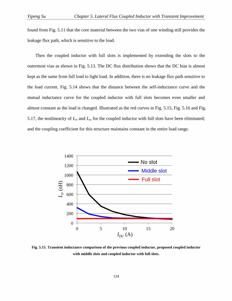
Yipeng Su Chapter 5. Lateral Flux Coupled Inductor with Transient Improvement
124
found from Fig. 5.11 that the core material between the two vias of one winding still provides the
leakage flux path, which is sensitive to the load.
Then the coupled inductor with full slots is implemented by extending the slots to the
outermost vias as shown in Fig. 5.13. The DC flux distribution shows that the DC bias is almost
kept as the same from full load to light load. In addition, there is no leakage flux path sensitive to
the load current. Fig. 5.14 shows that the distance between the self-inductance curve and the
mutual inductance curve for the coupled inductor with full slots becomes even smaller and
almost constant as the load is changed. Illustrated as the red curves in Fig. 5.15, Fig. 5.16 and Fig.
5.17, the nonlinearity of Ltr and Lss for the coupled inductor with full slots have been eliminated;
and the coupling coefficient for this structure maintains constant in the entire load range.
Fig. 5.15. Transient inductance comparison of the previous coupled inductor, proposed coupled inductor
with middle slots and coupled inductor with full slots.
Ltr
(nH
)
IDC (A)
0
200
400
600
800
1000
1200
1400
0 5 10 15 20
No slot
Middle slot
Full slot

Yipeng Su Chapter 5. Lateral Flux Coupled Inductor with Transient Improvement
125
Fig. 5.16. Steady state inductance comparison of the previous coupled inductor, proposed coupled inductor
with middle slots and coupled inductor with full slots.
Fig. 5.17. Coupling coefficient comparison of the previous coupled inductor, proposed coupled inductor with
middle slots and coupled inductor with full slots.
In summary, both the nonlinearity of the steady state inductance and the transient inductance
can be controlled by adding the slots into previous coupled inductor structure. The moderate
No slot
Lss
(nH
)
IDC (A)
0
200
400
600
800
1000
1200
1400
0 5 10 15 20
Middle slot
Full slot
-1
-0.8
-0.6
-0.4
-0.2
0
0 5 10 15 20
IDC (A)
No slot
α
2.42
2.10
1.79
1.51
1.12
1.00
Middle slot
Full slot

Yipeng Su Chapter 5. Lateral Flux Coupled Inductor with Transient Improvement
126
nonlinear inductance is realized by the middle slots structure, while the full slots structure
eliminates all the nonlinearity and achieves constant inductance values in the entire load range.
The stable coupling coefficient only can be achieved when reluctances of all flux paths are
insensitive to the load current. In order to reduce the light load transient inductance to improve
the transient response for the VR application, the light load steady state inductance, namely some
light load efficiency, has to be sacrificed. Fortunately, there are many advance control strategy to
realize the light load efficiency improvement, such as constant-on control, DCM operation by
diode emulation mode.
Besides the air slots, the low permeability magnetic material, whose permeability (µr∆) as a
function of DC bias (HDC) is almost constant value, also can be applied as the material of the
slots, to make the properties of the leakage flux path in the coupled inductor is insensitive to the
load. In addition, it gives another freedom to control the coupling coefficient and the nonlinearity
of the inductance curve, by tuning the relative permeability of the slots, which only can be one
for the air slots structure.
The transient performances of the coupled inductors with middle slots and with full slots are
also evaluated with the same simulated platform, which is used for the previous coupled inductor
structure. The AVP waveforms during the load transient for the coupled inductors with middle
slots and with full slots are shown in Fig. 5.18 and Fig. 5.19. It can be seen the undershoot
voltage spike is decreased significantly by adding the middle slots. The inductor current almost
can follow the required load current. For the coupled inductor with full slots, the inductor current
can exactly follow the required load current, the undershoot voltage spike therefore is totally
eliminated.

Yipeng Su Chapter 5. Lateral Flux Coupled Inductor with Transient Improvement
127
(a)
(b) (c)
Fig. 5.18. Evaluation of the transient performance of the coupled inductor with middle air slots:
(a) AVP waveform of the output voltage during transient, (b) Zoomed-in waveform during load step-up,
(c) Zoomed-in waveform during load step-down.
(a)
50uS/Div
11.6mV
10.7mV
Vo
ut(V
)
iload
iL1
Vout
Total iLCurr
en
t /
AC
urr
en
t /
AV
olta
ge
/
V
iload
iL1
Vout
Total iL
Cu
rre
nt /
AC
urr
en
t /
AV
olta
ge
/
V
50uS/Div
6.2mV
Vo
ut(V
)

Yipeng Su Chapter 5. Lateral Flux Coupled Inductor with Transient Improvement
128
(b) (c)
Fig. 5.19. Evaluation of the transient performance of the coupled inductor with full air slots:
(a) AVP waveform of the output voltage during transient, (b) Zoomed-in waveform during load step-up,
(c) Zoomed-in waveform during load step-down.
5.3 Experimental Verification of the Proposed Structure
In order to verify the proposed structure and the associated analysis, the planar cores for the
coupled inductors with slots are fabricated and tested. The dimensions of the core are labeled in
its conceptually drawing as Fig. 5.20, in which the surface copper traces of the coupled inductor
are intentionally hidden so that the core structure is clearly shown. The air slots are mechanically
cut between the vias of two coupled windings. Right now, the minimal value of the width of the
air slots can be cut is lg=0.7mm based on our fabrication capability. The FEA simulation shows
that further decreasing lg is beneficial to increase the inductance density and the optimal lg value
is around 0.2mm-0.3mm. The lg value smaller than 0.7mm can be achieved through the better
cutting techniques, or filling low permeability magnetic material into the air slots to equivalently
decrease the width of the air slots. In this dissertation, only the coupled inductors with 0.7mm air
slots are used to demonstrate the concept.
iload
iL1
Vout
Total iL
Curr
en
t /
AC
urr
en
t /
AV
olta
ge
/
V
iload
iL1
Vout
Total iL
Curr
en
t /
AC
urr
en
t /
AV
oltage /
V

Yipeng Su Chapter 5. Lateral Flux Coupled Inductor with Transient Improvement
129
Fig. 5.20. Proposed lateral flux coupled inductor with air slots (the surface copper traces are hidden).
(a) (b)
Fig. 5.21. Fabricated prototypes of the coupled inductors with slots:
(a) with middle air slots, (b) with full air slots.
The prototypes of the proposed “middle slots structure” and “full slots structure” are both
manufactured and illustrated in Fig. 5.21 (a) and Fig. 5.21 (b), respectively. In each figure, the
cores only without windings are shown in the left hand side and the cores with windings as the
coupled inductors are in the right hand side. The coupled inductors to be tested work as the
output inductors of a two-phase POL converter, and the current waveforms of inductors are
measured by a tiny rogowski coil, CWT Ultra-mini [87] developed by Power Electronic
Measurements (PEM). The measured current waveforms of the coupled inductor are shown in
Fig.5.22.
g=3mm
d=2.5mm
=0.7mm
h=1.8mm
Core only Coupled L Core only Coupled L

Yipeng Su Chapter 5. Lateral Flux Coupled Inductor with Transient Improvement
130
Fig. 5.22. Measured current waveforms of the tested coupled inductors.
(a) (b)
Fig. 5.23. Comparison between measured inductance and simulated inductance for:
(a) coupled inductor with middle air slots, (b) coupled inductor with full air slots.
Vsw_1
Vsw_2
iL_1
iL_2
T1 T2
Ipp_1
Ipp_2
0
100
200
300
400
500
600
700
0 5 10 15 20 25
Ind
uct
ance
(n
H)
IDC (A)
Lss
Ltr
0
100
200
300
400
500
600
700
0 5 10 15 20 25
Ind
uct
ance
(n
H)
IDC (A)
Lss
Ltr

Yipeng Su Chapter 5. Lateral Flux Coupled Inductor with Transient Improvement
131
The steady state inductance and transient inductance of the coupled inductor are essentially
the equivalent inductance during time intervals T1 and T2 illustrated in Fig. 5.22. By measuring
the peak-to-peak current ripple and the voltage second during different time intervals, Lss and Ltr
can be calculated with (5.1) and (5.2), where Vin and Vout are the input and output voltage of the
converter. The steady state inductance and transient inductance are measured as the dots in Fig. 5.
23. The measured inductance is also compared with the analytically predicted values, which are
shown as the curves in Fig. 5. 23. The good agreement between the measured and predicted
values validates that the proposed coupled inductor structure can well control the nonlinearity of
the inductance in the entire load range.
1_
11
)(
pp
outineqss
I
TVVLL
(5.1)
2_
22
pp
outeqtr
I
TVLL
(5.2)
The efficiencies of the two-phase POL converter with different coupled inductor designs are
measured and compared in Fig. 5.24. It can be seen the converter achieves exactly the same
efficiency at heavy load with different coupled inductors, while the coupled inductor with middle
slots improves the light load efficiency of the converter by 3%-5%, since it still maintains some
nonlinear inductance. To summarize the evaluation and comparison in this section, it is a trade-
off between the light load efficiency and the transient response when choosing different coupled
inductor structures. For the applications without any requirements for the transient performance
or the output capacitance, the coupled inductor with middle slots, or even the previous coupled
inductor can be used to improve the light load efficiency of the system. However, for the high

Yipeng Su Chapter 5. Lateral Flux Coupled Inductor with Transient Improvement
132
density VR application, where very fast transient speed is needed, the coupled inductor with full
slots has to be chosen to meet the transient requirement and minimize the number of output
capacitors. The light load efficiency of the converter also has to be sacrificed a little bit.
Fig. 5.24. Measured efficiencies of the two-phase POL converter with different coupled inductors.
5.4 Two-Phase Integrated POL Module with PCB Embedded Coupled
Inductor Substrate
After the proposed lateral flux coupled inductor with transient speed improvement has been
verified by the experimental measurement, the planar core for coupled inductor with full slots
shown in left hand side of Fig. 5.21 (b) is embedded into multi-layer PCB to demonstrate a high
density POL module with fast transient response for the laptop VR application. The 4-layer PCB
structure in Fig. 5.25 is designed for the two-phase PCB integrated POL module. Similar as the
single phase design, the top layer is the active layer for the connection of other components. The
planar core with full air slots is sandwiched between the third and the forth layers, which work as
the surface windings of the coupled inductor. The second layer is a shielding layer to block the
0.70
0.75
0.80
0.85
0.90
0.95
0 10 20 30 40 50
Eff
icie
ncy
Iout (A)
middle slots
full slots

Yipeng Su Chapter 5. Lateral Flux Coupled Inductor with Transient Improvement
133
electromagnetic interaction between inductor substrate and the active layer, and minimize the
parasitics in the high frequency switching loop of the POL converter. The 4oz copper is used for
the surface windings of the inductor while 2oz copper is chosen for the active and shielding
layers. Different from the single phase design, two ports connected to the terminals of the
inductor for the DCR sensing are implemented in the third layer as shown in Fig. 5.25.
Fig. 5.25. The expanded view of the 4-layer PCB structure for the two-phase 3D integrated
POL module with embedded coupled inductor.
Fig. 5.26. Two-phase 3D integrated POL module with PCB embedded coupled inductor substrate.
VSW1
Vout1
VSW2
Vout2
DCR sensing
coupled L
Shield

Yipeng Su Chapter 5. Lateral Flux Coupled Inductor with Transient Improvement
134
The prototypes of the two-phase PCB integrated POL module with embedded coupled
inductor are fabricated and shown in Fig. 5.26. Its efficiency is measured as the blue curve in Fig.
5.27. It is found a prominent efficiency drop at heavy load (5% at full load) compared with the
red curve, which is the efficiency of the converter tested with the non-embedded coupled
inductor shown in the right hand side of Fig. 5.21 (b). The efficiency drop at heavy load comes
from the significant increasing of the winding resistance after the coupled inductor being
embedded into PCB. As illustrated in Fig. 5.25, the winding of embedded coupled inductor for
each phase is constructed by two through vias, two blind vias and 4oz (0.14mm) surface traces.
In the conventional PCB vias, only 30µm copper is electroplated on the side wall of the vias for
the current conduction. The winding of non-embedded coupled inductor for each phase is
implemented by four solid pins and 0.25mm surface traces. The winding resistance breakdown
and comparison in Fig. 5.28 shows that the winding resistance is increased from 1.1mΩ to
4.3mΩ after the coupled inductor is embedded into PCB, which is mainly caused by the solid
pins are replaced by the conventional PCB through vias and blind vias.
Fig. 5.27. The efficiency comparison before and after the coupled inductor being embedded into PCB.
0.70
0.75
0.80
0.85
0.90
0.95
0 10 20 30 40 50
Eff
icie
ncy
Iout (A)
non-embedded
embedded
Gen. 1 embedded
Gen. 2

Yipeng Su Chapter 5. Lateral Flux Coupled Inductor with Transient Improvement
135
The solid pins can be inserted into the PCB through vias to reduce the resistance of the vias.
However, this solution is not doable for the blind vias. In next generation of two-phase PCB
integrated POL module, all of the vias will be implemented by the through vias and then the
solid pins will be inserted into these through vias. The 4oz copper is kept for the surface traces.
The evolution of the module designs from generation one to generation two is shown in Fig. 5.29.
By doing that, the projected winding resistance of next generation embedded coupled inductor
can be reduced to 1.8mΩ/phase. The projected efficiency of next generation POL module is
shown as the black curve in Fig. 5.27.
The power density achievements of the PCB integrated POL modules developed in chapter 4
and chapter 5 are summarized in Fig. 5.30. The magnetic integration based on embedded metal
flake composite material offers a simple and cost effective way to implement the high density
POL modules. The single-phase module achieves 600W/in3 power density with 20A output
current and the two-phase module achieves 800W/in3 power density with 40A output current.
Fig. 5.28. Winding resistance breakdown and comparison between the embedded
coupled inductor and non-embedded coupled inductor.
0.0
1.0
2.0
3.0
4.0
5.0
embedded winding
non-embedded winding
Blind
vias
through
vias4oz
Cu
Total DCR
win
din
g r
esis
tan
ce (
mΩ
)
Solid
pins
Solid
pins
0.25mm
Cu

Yipeng Su Chapter 5. Lateral Flux Coupled Inductor with Transient Improvement
136
Fig. 5.29. The evolution of the module designs from generation one to generation two.
Fig. 5.30. Power density achievements of the PCB integrated POL modules.
VSW1
VSW2
VSW1
VSW2
through via blind via
Gen. 1 Gen. 2
500
1A 20A10A
300
5A
100
40A
700
1000
Power
density
(W/in3)
15A Current30A
Power density is
calculated with 1.2Vout
The pictures are not
scaled to real size.
with IR’s GaN
with IR’s GaN
with EPC’s GaN

Yipeng Su Chapter 5. Lateral Flux Coupled Inductor with Transient Improvement
137
5.5 Summary
The huge light load transient inductance of the lateral flux coupled inductor proposed in
previous work, brings in a severe transient problem if it is used in the VR to power the micro-
processor, where very fast di/dt is needed. In order to improve the transient performance,
meanwhile keep the low profile design for the 3D PCB integrated POL module, the previous
coupled inductor structure is modified by adding the air slots into the leakage flux path. The
nonlinearity of the inductance can be controlled by different slots structure. More important, the
coupled inductor with air slots can achieve flat coupling coefficient in the entire load range.
Therefore, the benefit of inverse coupling for VR application can be fully utilized in the entire
load range. The coupled inductor with middle slots and with full slots are fabricated and tested,
in order to verify the predicted inductance by FEA simulation. In addition, the planar core with
full air slots is manufactured and sandwich into multi-layer PCB, to demonstrate a two-phase
integrated POL module with 800W/in3 and 40A output current, for laptop VR application.

Yipeng Su Chapter 6. Fundamental Study of the Planar Core with Variable Flux
138
Chapter 6.
Fundamental Study of the Planar Core
with Variable Flux
The planar inductor with lateral flux pattern has been successfully demonstrated as the
substrate for the high density 3D integrated POL module. Although the benefits of the lateral
flux inductor are validated in terms of high density and low profile, the flux distribution in such
planar core is very non-uniform and some parts of the core are pushed into saturation region,
which are totally against the conventional sense of inductor design based on flux uniformity. The
traditional design philosophy assumes the fully utilization of the core only can be achieved by
uniform flux. Any saturation would cause hot spots and worsen the performance of the core [65].
In the lateral flux inductor structure, is the saturated core detrimental for the inductor operation?
Does the saturated core introduce excessive core loss? Does the variable flux lead to non-
uniform distribution of the core loss density and localized hot spots? This chapter tries to answer
these questions and clarifies that the lateral flux planar inductor with variable flux distribution is
beneficial or impedimental for the high current POL application.
6.1 Non-uniform Flux Distribution in Lateral Flux Planar Inductor
The single-turn lateral flux inductor is essentially constructed by two lateral flux unit cells in
square as shown in Fig. 6.1 (a), which can be approximated and simplified by the circular shape
disc core in Fig. 6.1 (b), because of very little flux in the four corners [21]. With 20A DC current,

Yipeng Su Chapter 6. Fundamental Study of the Planar Core with Variable Flux
139
the DC flux distribution (HDC) of the disc core in Fig. 6.2 shows that the DC bias of the core
varies from several hundred to several thousand A/m. The inner part of the disc close to the
exciting current is biased at relatively high DC flux, while the edge of the disc far away from the
excitation is operated at lower DC bias. If the core material is homogeneous, the HDC value can
be calculated by Ampere’s Law in (6.1), which is only related to the DC bias current (IDC) and
the radius of the circular flux path (r).
(a) (b)
Fig. 6.1. Half core of the single-turn lateral flux inductor: (a) unit cell in square, (b) disc core in circle.
𝐻𝐷𝐶 =𝑁 ⋅ 𝐼𝐷𝐶2𝜋𝑟
(6.1)
Once the core material is determined, the large DC bias range of the disc core also can be
reflected on the B-H curve of the magnetic material. For example, the different operating points
of the disc core are associated with the B-H curve of the metal flake composite material from
NEC/Tokin in Fig. 6.3. It can be seen that the innermost part of the disc is pushed to more than
90% of the saturation flux density (Bsat), which would never happen in conventional inductor
design with uniform flux. Besides the variable DC flux, the permeability of the core, which is the
slope at a given operating point, is also non-uniform distributed. The SF metal flake composite
with non-linear permeability is used as the core material for the following discussion. The
conclusion can be extended to other magnetic materials according to the same analytical process.
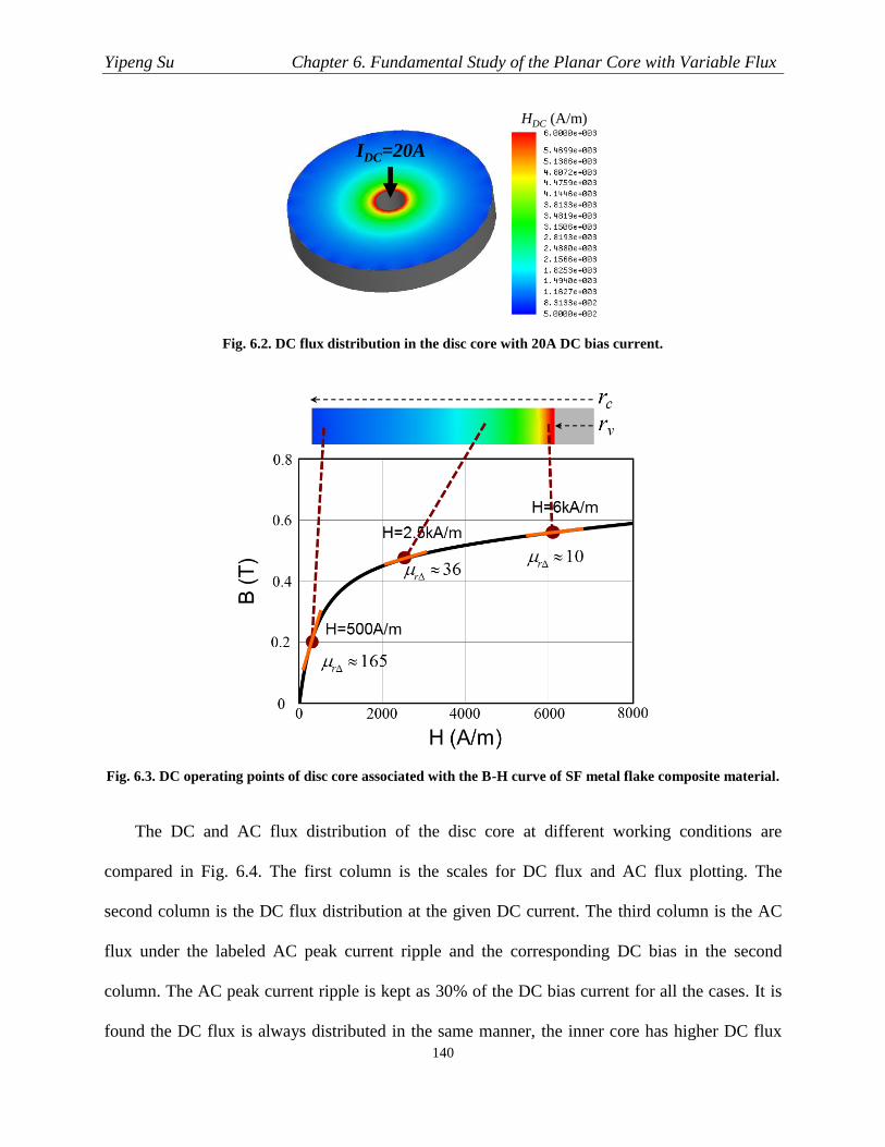
Yipeng Su Chapter 6. Fundamental Study of the Planar Core with Variable Flux
140
Fig. 6.2. DC flux distribution in the disc core with 20A DC bias current.
Fig. 6.3. DC operating points of disc core associated with the B-H curve of SF metal flake composite material.
The DC and AC flux distribution of the disc core at different working conditions are
compared in Fig. 6.4. The first column is the scales for DC flux and AC flux plotting. The
second column is the DC flux distribution at the given DC current. The third column is the AC
flux under the labeled AC peak current ripple and the corresponding DC bias in the second
column. The AC peak current ripple is kept as 30% of the DC bias current for all the cases. It is
found the DC flux is always distributed in the same manner, the inner core has higher DC flux
HDC (A/m)
IDC=20A
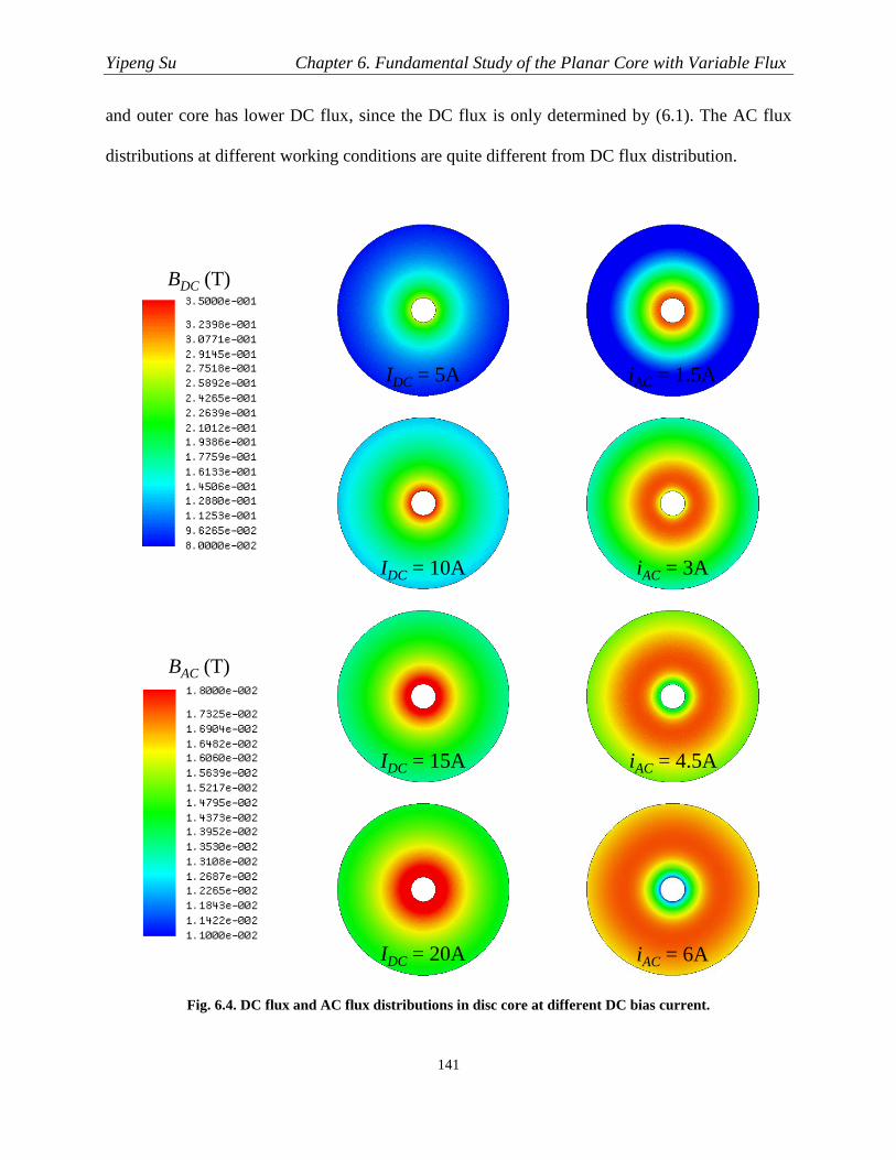
Yipeng Su Chapter 6. Fundamental Study of the Planar Core with Variable Flux
141
and outer core has lower DC flux, since the DC flux is only determined by (6.1). The AC flux
distributions at different working conditions are quite different from DC flux distribution.
Fig. 6.4. DC flux and AC flux distributions in disc core at different DC bias current.
BDC (T)
IDC = 5A iAC = 1.5A
IDC = 10A iAC = 3A
BAC (T)
IDC = 15A iAC = 4.5A
IDC = 20A iAC = 6A

Yipeng Su Chapter 6. Fundamental Study of the Planar Core with Variable Flux
142
When DC bias current is lower, such as 5A and 10A, the pattern of AC flux distribution is
similar as that of DC flux, namely the inner flux is higher and outer flux is lower. If the DC bias
current becomes high enough, like 15A and 20A, to saturate the inner part of the disc core, most
of the AC flux has been pushed to the outer part of the disc core. Because the permeability of the
inner saturated core becomes much lower, its magnetic reluctance is increased significantly, even
though it has shorter flux path. The AC flux will automatically avoid the saturated core, where
the reluctance is large. Only every little AC flux is left in this region with high DC flux. This DC
and AC flux counterbalance mechanism actually limits the AC flux, as well as the core loss in
the saturated core, which makes the saturation not detrimental any more.
(a)
(b)
Fig. 6.5. Lateral flux inductor with different number of turns:
(a) 3D drawing of the real construction, (b) Top view of the half core (r: radial direction).
The DC and AC flux auto-balanced phenomenon also can be found in multi-turn structures
of the lateral flux inductor. Fig. 6.5 (a) shows the real construction of the lateral flux inductor
with different number of turn (N). Due to symmetry, the inductors can be divided into two
identical half-cores, whose top views are illustrated in Fig. 6.5 (b). The amplitude of DC flux and
N=1 N=2 N=3
r r r
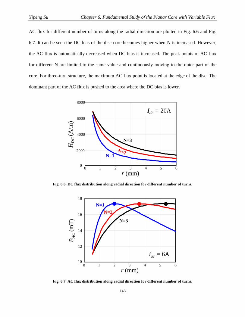
Yipeng Su Chapter 6. Fundamental Study of the Planar Core with Variable Flux
143
AC flux for different number of turns along the radial direction are plotted in Fig. 6.6 and Fig.
6.7. It can be seen the DC bias of the disc core becomes higher when N is increased. However,
the AC flux is automatically decreased when DC bias is increased. The peak points of AC flux
for different N are limited to the same value and continuously moving to the outer part of the
core. For three-turn structure, the maximum AC flux point is located at the edge of the disc. The
dominant part of the AC flux is pushed to the area where the DC bias is lower.
Fig. 6.6. DC flux distribution along radial direction for different number of turns.
Fig. 6.7. AC flux distribution along radial direction for different number of turns.
r (mm)
HD
C(A
/m)
01 2 3 4 5 6
2000
4000
6000
8000
0
N=1
Idc = 20A
N=3
BA
C(m
T)
r (mm)
101 2 3 4 5 6
12
14
16
18
0
iac = 6A
N=1
N=3
N=2

Yipeng Su Chapter 6. Fundamental Study of the Planar Core with Variable Flux
144
The core loss density (Pv) is usually determined by both DC flux and AC flux. General
speaking, either higher DC flux or higher AC flux causes larger core loss density. Because of the
variable DC and AC flux distributed in the disc core, the distribution of the core loss density
should be also non-uniform. The distribution of core loss density in the disc core is modeled
based on the same approach in [63]. The equations to calculate Pv are list as (6.2) and (6.3),
which are the evolution of the Modified Steinmetz Equation (MSE) developed for the high
current POL application. The first part of (6.2) in red is the impact of triangular exciting current
on core loss density, where D is the duty cycle. The second blue part considers the impact of DC
bias on core loss, which is derived as a polynomial of HDC from measured data. The last black
part of (6.2) is Original Steinmetz Equation (OSE).
𝑃𝑣 = [2
𝜋2 ⋅ 𝐷 ⋅ (1 − 𝐷)]𝛼−1
⋅ 𝐹(𝐻𝐷𝐶) ⋅ 𝑘 ⋅ 𝐵𝐴𝐶𝛽⋅ 𝑓𝑠
𝛼 (6.2)
where 𝑘 = 0.0032, 𝛼 = 1.546, 𝛽 = 2.458 for SF metal flake composite
𝐹(𝐻𝐷𝐶) = −2.7𝑒−20 ⋅ 𝐻𝐷𝐶5 + 1.4𝑒−15 ⋅ 𝐻𝐷𝐶
4
−2.4𝑒−11 ⋅ 𝐻𝐷𝐶3 + 1.7𝑒−7 ⋅ 𝐻𝐷𝐶
2
−6.3𝑒−5 ⋅ 𝐻𝐷𝐶 + 1
(6.3)
The core loss density of the disc core is plotted along the radial direction in Fig. 6.8, for
different number of turns. The Pv is calculated for the inductor in POL converter working at
Vin=12V, Vout=1.2V, Iout =20A, iac=6A and fs=2MHz. It can be seen that the innermost saturated
core essentially does not create excessive core loss density. The maximum core loss density
occurs in some place with moderate DC bias. From the outer part to the inner part of the core, the
core loss density is increased first and then decreased. The peak points of Pv for different N have

Yipeng Su Chapter 6. Fundamental Study of the Planar Core with Variable Flux
145
been also kept as the same value shown in Fig. 6.8. In summary, the DC and AC flux
counterbalance mechanism actually limits the core loss density in the saturated core. The core
saturation therefore becomes not detrimental any more in this special structure.
Fig. 6.8. Core loss density along radial direction for different number of turns.
6.2 Evaluation of the Core Utilization
After understanding the radial distributed field in lateral flux inductor, [21] [62] [63]
proposed and validated the inductance and core loss modeling methods by dividing the half core
in Fig. 6.5 (b) into a series of concentric infinitesimal rings and ignoring the flux in the four
corners. The shapes of the rings are circular for one-turn and elliptical for multi-turn. The total
flux and core loss of half core are the integral of that of each infinitesimal ring. In this section,
the inductance density (Ldensity) and performance factor (Pf) are proposed to evaluate the core
utilization of each infinitesimal ring. Actually, both the Ldensity and Pf are the variable functions
along the radial direction of half core, similar as the non-uniform distributed flux and core loss
density. Higher Ldensity or Pf means better utilization of the core.
Pv
(kW
/m3)
r (mm)
4001 2 3 4 5 6
800
1200
1600
2000
0
Vin = 12V
Vout = 1.2V
fs = 2MHz
N=1
N=2
N=3

Yipeng Su Chapter 6. Fundamental Study of the Planar Core with Variable Flux
146
The inductance density is defined as the contributed inductance of the small ring divided by
its volume. In order to meet a required inductance, smaller core volume can be achieved by using
the core with higher Ldensity. As one example, the equation to calculate the inductance density
distribution of one-turn lateral flux inductor is elaborated in (6.4), where r is the radius of the
infinitesimal ring, Δr and h are the width and thickness of the ring core.
𝐿𝑑𝑒𝑛𝑠𝑖𝑡𝑦(𝑟) =∆𝐿
∆𝑉=
𝜇0 ⋅ 𝜇𝑟(𝑟) ⋅ ∆𝑟 ⋅ ℎ2𝜋𝑟⁄
∆𝑟 ⋅ ℎ ⋅ 2𝜋𝑟=𝜇0 ⋅ 𝜇𝑟(𝑟)
(2𝜋𝑟)2
(6.4)
The performance factor is defined as the ratio between the inductance of a small ring and its
core loss. Basically, Pf is a criterion to quantify how much inductance can be obtained when unit
core loss is paid. Higher Pf value is preferred, because less core loss needs to be paid, in order to
achieve a given inductance. If both the inductance and the core loss are divided by the volume of
a small ring, the performance factor can be evolved as the ratio of the inductance density to the
core loss density, as illustrated in (6.5).
𝑃𝑓(𝑟) =∆𝐿
∆𝑃𝑐𝑜𝑟𝑒=
∆𝐿∆𝑉⁄
∆𝑃𝑐𝑜𝑟𝑒∆𝑉⁄
=𝐿𝑑𝑒𝑛𝑠𝑖𝑡𝑦
𝑃𝑣
(6.5)
The inductance density and performance factor along the radial direction of the half core for
different number of turns are shown in Fig 6.9 and Fig. 6.10. The Ldensity value is always
increased by moving the core closer to the excitation. When r is decreased, the permeability of
the core although becomes smaller due to the higher DC bias, the reduction of the denominator
of (6.4) (i.e. (2πr)2) is even much more. The inductance density of the core is actually increased
when it is pushed to higher DC bias. The Pf curves in Fig. 6.10 are derived from the Ldensity

Yipeng Su Chapter 6. Fundamental Study of the Planar Core with Variable Flux
147
curves in Fig.6.9 divided by the Pv curves in Fig. 6.8. Since the incremental Ldensity when r is
decreased is larger than that of Pv. The inner part of the core biased at higher DC flux actually
has higher performance factor. Especially on the left side of the peak point of Pv curves, the core
loss density begins to drop, while the inductance density keeps increasing, the performance
factor becomes much higher in this region.
Fig. 6.9. Inductance density along radial direction for different number of turns.
Fig. 6.10. Performance factor along radial direction for different number of turns.
r (mm)1 2 3 4 5 60
Lden
sity
(nH
/mm
3)
0
0.5
1.0
1.5
Idc = 20A
N=3
N=1
r (mm)1 2 3 4 5 60
N=3
N=1
IDC=20A
iac=6A
Vin = 12V
Vout = 1.2V
fs = 2MHz
0
0.2
1.0
0.4
0.6
0.8
Pf(n
H/m
W)

Yipeng Su Chapter 6. Fundamental Study of the Planar Core with Variable Flux
148
In summary, in the lateral flux planar core with variable flux, the inner core biased at higher
DC flux can better utilize the core material due to higher inductance density and performance
factor. However, the single operating point of the conventional core with constant flux cannot be
pushed to the saturation region, thus the core utilization cannot be as good as the variable flux
core.
6.3 Thermal Evaluation of the Planar Core with Variable Flux
Even through the DC flux and AC flux in the lateral flux planar core can automatically
balance each other, Fig. 6.8 indicates that the distribution of the core loss density is still non-
uniform. Does the variable core loss density cause any localized hot spots and thermal problems?
In this section, the temperature distribution of the planar core is studies by FEA steady state
thermal simulation and the experimental measurement, which are performed on several design
examples of the lateral flux inductors for a specific POL converter.
First, the inductors are designed for a POL converter, working at Vin=12V, Vout=1.2V, Iout
=20A, iac=6A and fs=2MHz. The required inductance is calculated to be 90nH. Two planar disc
cores in Fig. 6.1 are placed side by side to construct the one-turn lateral flux inductor. There are
only two dimensional parameters, core size rc and core thickness h, to be determined, if the via
size has been fixed as rv=0.5mm. Based on the inductance model in [21] [62], different
combinations of rc and h to achieve constant 90nH inductance are derived in Fig. 6.11. It is
found a design trade-off between rc and h, such as design A with smaller rc and larger h, design
C with larger rc and smaller h, as well as the design B in between.

Yipeng Su Chapter 6. Fundamental Study of the Planar Core with Variable Flux
149
Secondly, the Pv distribution along the radial direction for the three designs are plotted in
Fig. 6.12. .It should note that the Pv distribution is only determined by the working condition of
the inductor in the converter, such as DC bias, AC ripple and frequency. Therefore, the Pv curves
for design A, B, C are overlapped at the starting points, their ending points are different. It can be
seen from Fig. 6.12, the non-uniformity of Pv becomes more significant when the core size, rc, is
increased. For design C, the maximum Pv is almost 3 times of the minimum Pv.
Fig. 6.11. Different combination of rc and h to achieve constant 90nH.
Fig. 6.12. Pv distribution along radial direction for disc core designs A, B and C.
0
2
4
6
80 2 4 6
rv=0.5mm
rc (mm)
h(m
m)
AB
C
Pv
(kW
/m3)
r (mm)
400
800
1200
1600
2000
0 2 4 6 8
Crc=8mm
BA
rc=3mm
rc=5mm

Yipeng Su Chapter 6. Fundamental Study of the Planar Core with Variable Flux
150
Fig. 6.13. FEA thermal simulation model for planar core with variable Pv based on concentric ring concept.
The steady state thermal simulation models to study the temperature distribution of planar
cores A, B and C are built in ANSYS as illustrated in Fig. 6.13. In order to emulate the non-
uniform Pv distribution, the disc core is divided into a series of concentric circular rings, in
which the Pv is assumed to be uniform. Each ring is regarded as one heat source with heat flow
exchanging each other. The power loss is applied to each ring individually. The thermal
conductivity of the metal flake composite material is 7.5W/(mK). The simulations are executed
with 25ºC ambient temperature and without forced airflow
The simulated temperature distribution on the different disc cores are shown in Fig. 6.14.
ΔTc is the difference between the peak temperature and valley temperature of the core. For all of
the studied cases, ΔTc is always below 2ºC, which indicates the temperature of the core can be
regarded as uniform distributed. The average value of the core loss density (Pv_avg) is calculated
as the total core loss over the core volume. The average temperature for each core is also marked
in Fig. 6.14, which is found to be almost directly proportional to the Pv_avg value of each core.

Yipeng Su Chapter 6. Fundamental Study of the Planar Core with Variable Flux
151
(a)
(b)
(c)
Fig. 6.14. Thermal evaluation of the planar disc core with variable distributed Pv :
(a) for core design A, (b) for core design B, (c) for core design C.
25˚C 80˚C
ΔTc = 0.4˚C76˚C
25˚C 80˚C
61˚CΔTc = 0.8˚C
25˚C 80˚C
45˚CΔTc = 1.2˚C

Yipeng Su Chapter 6. Fundamental Study of the Planar Core with Variable Flux
152
(a) (b)
Fig. 6.15. Experimental measurement of the temperature distribution of the disc core:
(a). Fabricated prototype, (b) measured thermal image.
A prototype of one-turn lateral flux inductor is fabricated according to the dimensions of
disc core design B as shown in Fig. 6.15 (a). Its temperature distribution is recorded by thermal
camera when it works as the output inductor of the POL converter working at the same
specification as previous calculation and simulation, Vin=12V, Vout=1.2V, Iout =20A, iac=6A and
fs=2MHz. Therefore, the Pv distribution in the core should follow the calculated Pv curve for
design B in Fig. 6.12. The thermal image of the one-turn inductor is shown in Fig. 6.15 (b),
which also proves there is no significant temperature variation on the planar core with variable
Pv distribution. The good agreement between the measured core temperature (56ºC) and the
simulated core temperature (61ºC) validates the accuracy of the FEA thermal simulation models.
It can be seen from Fig. 6.8, the non-uniformity of Pv in one-turn structure is the most
significant. If the uniform temperature has been concluded for the one-turn structure, the
conclusion can be extended to the multi-turn structure, in which the distribution of Pv is
relatively uniform. To summarize the analysis in this section, the planar core of the lateral flux
inductor has almost uniform temperature. No localized hot spots are found despite of 2-3 times
difference in core loss density.

Yipeng Su Chapter 6. Fundamental Study of the Planar Core with Variable Flux
153
6.4 Comparison between the Variable Flux Core and the Uniform Flux Core
In this section, both the lateral flux inductor with variable flux and conventional design with
uniform flux are designed and compared for the same POL converter working at Vin=12V,
Vout=1.2V, Iout=20A, iac=6A and fs=2MHz. The toroidal core shown in Fig. 6.16 is selected to
represent the uniform flux design. The width of the toroidal, w, is chosen as 2mm, in order to
achieve relatively uniform flux in the core. Actually, the magnetic field and core loss density of
this structure is only controlled by the average radius of the toroidal (ravg). By controlling ravg,
the DC bias is determined by Ampere’s Law in (6.1), and then the permeability of the core is
obtained according to the relationship between permeability and DC bias. The length of the
toroidal is derived by the required inductance value, 90nH. Finally, the AC flux and core loss
density can be calculated based on the core structure and the specifications of the converter. The
one-turn lateral flux inductor is designed following the approach proposed in [21]. The total core
loss, core volume and average core loss density, controlled by the core size, rc, are considered in
the design procedure.
Fig. 6.16. Toroidal core with relatively uniform flux distribution.
HDC (A/m)
ravg
w
l

Yipeng Su Chapter 6. Fundamental Study of the Planar Core with Variable Flux
154
The temperatures of the core as a function of average core loss density (Pv_avg) for these two
different structures are compared in Fig. 6.17. It can be seen that the planar disc core has lower
core temperature than the toroidal core when they are designed to be the same Pv_avg. In another
word, the planar disc core can handle higher Pv_avg than toroidal core if they are targeted to be the
same core temperature. The key reason is that the toroidal core is in a cubic shape, which is
usually found in the one-turn surface mounted inductor. While the lateral flux inductor spreads
the core in a horizontal plane. Therefore, the planar structure has larger surface area than the
conventional design to dissipate the heat.
Fig. 6.17. Core temperature as a function of core loss density for different inductor structures.
The core loss and the core volume of the planar disc core are shown as a function of core
size rc in Fig. 6.18 and Fig. 6.19. Reducing rc leads to lower core loss and smaller core volume.
However, the core thickness becomes larger and the core temperature is higher (due to higher
Pv_avg). The similar design trend can be found for the toroidal inductor. By decreasing ravg, lower
core loss and smaller core volume can be achieved, but the temperature of the core is sacrificed
due to higher Pv_avg.
Tc
(˚C
)
Pv_avg (kW/m3)
25
35
45
55
65
75
85
400 600 800 1000 1200 1400 1600 1800
disc core
A
B
TA=25˚C
No air flow
#1thermal limit

Yipeng Su Chapter 6. Fundamental Study of the Planar Core with Variable Flux
155
Fig. 6.18. Core loss comparison between disc core and toroidal core.
Fig. 6.19. Core volume comparison between disc core and toroidal core.
Two approaches are used to compare the performances of the disc core with variable flux
and the toroidal core with uniform flux. In the first comparison, 75ºC core temperatures is
assumed to be the thermal limit for both the disc core and toroidal core. It can be seen from Fig.
6.17, the toroidal core #1 and the disc core A already hit the design limit in terms of thermal
constraint. Then the core loss and core volume of toroidal core #1 and disc core A are compared
rc (mm)
Co
re L
oss
(mW
)
02 4 6 80
200
400
600
AB
Toroidal #1
rc (mm)
Co
re V
olu
me
(mm
3)
2 4 6 800
200
400
600
A
B
Toroidal #1

Yipeng Su Chapter 6. Fundamental Study of the Planar Core with Variable Flux
156
in Fig. 6.18 and Fig. 6.19, respectively. To keep the same maximum acceptable core temperature,
the disc core design achieves both smaller core loss and core volume compared with the toroidal
core design, since the average core loss density of disc core A is higher than that of toroidal core
#1.
Fig. 6.20. Core loss comparison between disc core and toroidal core in the entire load range.
In the second comparison, a conservative disc core design B in Fig. 6.18 and Fig. 6.19 is
used to achieve the same core loss and similar core volume as the toroidal core #1, but the core
temperature of the disc core B is more than 10ºC lower than that of the toroidal core #1 shown in
Fig. 6.17. So far, the core losses are only compared when the inductors are operated at full load
condition (20A). Fig. 6.20 extends the comparison of the core loss in the entire load range, from
which it can be seen the different inductors have the same core loss at full load, but the core loss
reduction at light load of the disc core B is more than that of toroidal core #1. In Fig. 6.20, the
curves are calculated values and dots are measured results. The uniform AC flux in the toroidal
core is clamped by the voltage-second of the POL converter, which is independent on the load
current. Its core loss is only decreased by the lower DC bias at light load.
0 5 10 15 20100
150
200
250
300
350
400
Co
re L
oss
(mW
)
IDC (A)
toroidal core #1
disc core B
calculated
measured

Yipeng Su Chapter 6. Fundamental Study of the Planar Core with Variable Flux
157
Fig. 6.21. AC flux distribution along the radial direction of disc core B at different load currents.
Fig. 6.22. Core loss density distribution along the radial direction of disc core B at different load currents.
The AC flux of the disc core is redistributed when the load current is decreased as shown in
Fig. 6.21. As discussed in previous section, most of the AC flux is pushed to the outer part of the
disc at heavy load, since the inner core is saturated. When the load current is decreased, the AC
flux is moved to the inner part of the disc. Because of that, the core loss density of inner core is
increased while the loss density of outer core is decreased as illustrated in Fig. 6.22. It also
0 1 2 3 4 510
15
20
25
BA
C(m
T)
r (mm)
5A
20A
0
1000
2000
3000
4000
0 1 2 3 4 5
5A
20A
Pv
(kW
/m3)
r (mm)

Yipeng Su Chapter 6. Fundamental Study of the Planar Core with Variable Flux
158
should notice that the total core volume of the disc core is dominated by the outer part of the disc.
The reduction of the core loss density of outer disc is beneficial to save more total core loss at
light load, even though the core loss of inner disc is increased a little bit. From heavy load to
light load, the planar disc core with variable flux has more core loss reduction than the toroidal
core with uniform flux, due to the AC flux and core loss density redistributions.
6.5 Summary
The planar inductor structure with lateral flux pattern provides low profile and high density
magnetic substrate for the high current 3D integrated POL module. However, the variable flux
distribution in the core goes against the conventional sense of the inductor design, which always
tries to achieve the flux uniformity. It seems like the utilization of the core in the lateral flux
inductor is poor. This chapter explores the field distribution, and then reveals the DC and AC
flux counterbalance mechanism in this lateral flux planar core, by which the AC flux as well as
the core loss density in the saturated core are limited. The saturation does not create the
excessive core loss and therefore is not detrimental any more. The inductance density and
performance factor are proposed as the criteria to evaluate the utilization of the core. It is found
that the inner part of the planar core, which is operated at higher DC bias actually has better core
utilization. The variable flux core takes the advantage of the saturated core safely, while the
constant flux core is not able to operate the entirely core in saturation region. Finally, the thermal
performance of the variable flux planar core is investigated by the FEA simulation and
experimental measurement. The temperature distribution over the core is almost uniform despite
of 2-3 times difference in core loss density. Because of the better thermal management capability,
the planar core can be pushed to higher core loss density level than the toroidal core with

Yipeng Su Chapter 6. Fundamental Study of the Planar Core with Variable Flux
159
relatively uniform flux, to realize lower total core loss and smaller core volume. In addition, the
planar core saves more core loss at light load than the toroidal core, due to the the AC flux and
core loss density redistributions.

Yipeng Su Chapter 7. Conclusions and Future Work
160
Chapter 7.
Conclusions and Future Work
7.1 Conclusions
Point-of-load (POL) converters have been used extensively in IT products. Today, almost
every microprocessor is powered by a multi-phase POL converter with high output current,
which is also known as voltage regulator (VR). In the state-of-the-art VRs, the circuits are
mostly constructed with discrete components and situated on the motherboard, where it can
occupy more than 1/3 of the footprint of the motherboard. A compact POL is desirable to save
precious space on motherboards to be used for some other critical functionalities. Recently,
industry has released many modularized POL converters, in which the bulky inductor is
integrated with the active components to increase power density. This concept has been
demonstrated at current levels less than 5A and power density around 600-1000W/in3. This
might address the needs of small hand-held equipment such as smart phones, but it is far from
meeting the needs for the applications such as laptops, desktops and servers, where tens and
hundreds of amperes are needed.
The large thickness of the conventional discrete inductor becomes the bottleneck for the
high current POL converter to achieve high power density. The lateral flux LTCC inductor can
be used as the substrate of the 3D integrated POL module to improve the power density. The size
of the LTCC inductor substrate can be continuously reduced by further pushing the operating
frequency. The impact of the multi-MHz operation on the inductor design is analyzed. Based on

Yipeng Su Chapter 7. Conclusions and Future Work
161
the trade of between core thickness and inductor loss, 3-turns inductor is used for POL module
with EPC’s GaN devices, which is operated from 1MHz to 3MHz. The 2-turns inductor is
preferred for the POL module with IR’s GaN devices running from 3MHz to 5MHz. The high
frequency operation reduces the number of LTCC tape layer to build the inductor substrate, and
the number of turns of the inductor. The fabrication process of the inductor is simplified and the
inductor cost is also decreased. The LTCC inductor substrates working at different frequency are
fabricated and tested on the high frequency POL converter. The measured efficiency and power
density of the module with LTCC inductors are compared with that with some commercial
discrete inductors. It is experimentally demonstrated several benefits of the LTCC inductor, such
as light load efficiency improvement, high power density and capability of integration. The 12V
to 1.2V, 10A-15A integrated POL modules with LTCC inductor substrate achieve more than 85%
efficiency and 800W/in3 power density at the multi-MHz operation.
The performance of the lateral flux inductor substrate can be improved by inverse coupling.
In order to design and analyze the two-phase inverse coupled inductor with very non-uniform
distributed flux, the FEA inductance and core loss models are established. The incremental
inductance is calculated through two-step magneto static simulations with small perturbation;
and the core loss is evaluated by the EEL core loss model with improved DC bias term. With
inversed coupling, the core volume can be reduced by 40% due to the DC flux cancellation. In
addition, lower DC bias leads to the smaller core loss density. However, the smaller core
thickness of the coupled inductor crowds the AC flux density and increases the core loss density.
These two effects balance each other and keep the core loss density of the inverse coupled
inductor at a similar level as that of the non-coupled inductor. However, the inverse coupling can
still reduce the core loss at full load condition, which is mainly coming from the core volume

Yipeng Su Chapter 7. Conclusions and Future Work
162
shrink. The power density of the integrated POL module with LTCC coupled inductor can be
pushed above 1kW/in3 at 5MHz, which is around 5-8 times of the power density of state-of-the-
art alternatives with the same current level.
The ceramic-based integration has not been widely adopted in industry products, since it is
not cost effective and some high temperature fabrication process is involved. The later work
validates the feasibility of using SENFOLIAGE (SF) metal flake composite for the high
frequency PCB integrated POL module. The compatibility of the flake material with
conventional PCB manufacturing technique is studied. After being sandwiched into FR4 epoxy
layers, the key properties of the SF flake core are not changed significantly. As a demonstration,
the 20A, MHz integrated POL modules are designed and fabricated based on a simple and cost
effective 4-layer PCB substrate with embedded magnetic layer, which achieve more than 85%
efficiency and 600W/in3 power density. The thermal performance of the module is evaluated by
measurement and simulation. The PCB integrated POL module is thermally limited by the active
device, rather than the embedded magnetics. The embedded core and winding do not create any
hot spots. The PCB integrated POL module survives after hundreds of thermal cycles, validating
the reliability and compatibility of the flake magnetic material with PCB integration. In addition,
the application of standard PCB process reduces the cost for manufacturing such integrated
modules due to the easy automation and low temperature process.
The huge light load transient inductance of the lateral flux coupled inductor proposed in
previous work, brings in a severe transient problem if it is used in the VR to power the micro-
processor, where very fast di/dt is needed. In order to improve the transient performance,
meanwhile keep the low profile design for the 3D PCB integrated POL module, the previous
coupled inductor structure is modified by adding the air slots into the leakage flux path. The

Yipeng Su Chapter 7. Conclusions and Future Work
163
nonlinearity of the inductance can be controlled by different slots structure. More important, the
coupled inductor with slots can achieve flat coupling coefficient in the entire load range.
Therefore, the benefit of inverse coupling for VR application can be fully utilized in the entire
load range. The coupled inductor with middle slots and with full slots are fabricated and tested,
in order to verify the predicted inductance by FEA simulation. The planar core with full air slots
is manufactured and sandwich into multi-layer PCB, to demonstrate a two-phase integrated POL
module with 800W/in3 and 40A output current, for laptop VR application.
The planar inductor structure with lateral flux pattern provides low profile and high density
magnetic substrate for the high current 3D integrated POL module. However, the variable flux
distribution in the core goes against the conventional sense of the inductor design, which always
tries to achieve the flux uniformity. The final part of this dissertation explores the field
distribution, and then reveals the DC and AC flux counterbalance mechanism in this lateral flux
planar core. Because of that, the AC flux and the core loss density in the saturated core are
limited. The saturation does not create the excessive core loss and therefore is not detrimental
any more. The inductance density and performance factor are proposed as the criteria to evaluate
the utilization of the core. It is found that the inner part of the planar core, which is operated at
higher DC bias actually has better core utilization. The variable flux core takes the advantage of
the saturated core safely, while the constant flux core is not able to operate the entirely core in
saturation region. The thermal performance of the variable flux planar core is investigated by the
FEA simulation and experimental measurement. The temperature distribution over the core is
almost uniform despite of 2-3 times difference in core loss density. Because of the better thermal
management capability, the planar core can be pushed to higher core loss density level than the
toroidal core with relatively uniform flux, to realize lower total core loss and smaller core

Yipeng Su Chapter 7. Conclusions and Future Work
164
volume. In addition, the planar core saves more core loss at light load than the toroidal core, due
to the the AC flux and core loss density redistributions.
7.2 Future Work
The lateral flux planar inductor substrate built with LTCC ferrite or PCB embedded SF core
shows promise for 3D integrated high current POL module. Following this path, there are still
some remaining works can be done to improve this dissertation:
1. The 40A two-phase POL module with PCB embedded coupled inductor substrate designed
and fabricated in chapter 5 still has too large winding resistance, which leads to significant
efficiency drop at heavy load. The related solution has been preliminarily proposed.
Therefore, the next generation two-phase PCB integrated POL module should be fabricated
and evaluated to verify the proposal.
2. The evaluation of the two-phase PCB integrated POL module only covers the open loop
testing. In the future work, the high density and fast transient speed VR platform should be
demonstrated for laptop application, by combining the modules and the advanced controller.
3. The PCB integrated magnetic components can be extended to some other areas, such as the
PCB embedded transformer substrate for isolated DC-DC converters, PCB embedded
capacitors, and furthermore the PCB embedded EMI filters.

Yipeng Su References
165
Reference
[1] www.semiconductors.org
[2] Texas Instrument, “LMZ10501 1A SIMPLE SWITCHER® Nano Module with 5.5V
Maximum Input Voltage,” LMZ10501 datasheet, May 2011 [Revised Jan. 2014].
[3] Murata, “Product brief LXDC series µDCDC converters,” 2014.
[4] Enpirion Power – Altera, “EN5366QI 6A PowerSoC voltage mode synchronous buck
PWM DC-DC converter with integrated inductor external output voltage programming,”
EN5366QI datasheet, Oct. 2013.
[5] Texas Instruments, “10A SIMPLE SWITCHER® power module with 2.95V-17V input and
current sharing in QFN package,” LMZ31710 datasheet, Jul. 2013.
[6] Linear Technology, “LTM4627 15A DC/DC µModule regulator,” LTM4627 datasheet,
2010.
[7] Murata Power Solutions, “OKL2-T/20-W12 series programmable output 20A iLGA SMT
PoL DC-DC converters,” OKL2-T/20-W12P2-C datasheet, 2014.
[8] Delta Electronics, “D12S1R830, non-isolated, power block DC/DC power modules:
7.0~13.2Vin, 0.8V~1.8V/30Aout,” D12S1R830D datasheet, Jan. 2011.
[9] Delta Electronics, “D12S72, non-isolated, power block DC/DC power modules:
7.0~13.2Vin, 0.8V~1.8V/40Aout,” D12S72C datasheet, Mar. 2011.
[10] Roger Allan, “New materials permit inductors to keep pace with smaller systems,” Power
Electronics Technology, Feb. 2009, pp. 26-29.
[11] Haswell (microarchitecture), en.wikipedia.org/wiki/Haswell_(microarchitecture)
[12] Pentium 4, en.wikipedia.org/wiki/Pentium_4
[13] Intel, “Votage regulator module (VRM) and enterprise voltage regulator-down (EVRD)
Yipeng Su References
166
11.1 design guidelines,” Sept. 2009.
[14] Xunwei Zhou, “Low-voltage high-efficiency fast-transient voltage regulator module,”
Ph.D. dissertation, Virginia Tech., Blacksburg, VA, Jul. 1999.
[15] Peng Xu, “Multiphase voltage regulator modules with magnetic integration to power
microprocessors,” Ph.D. dissertation, Virginia Tech., Blacksburg, VA, Jan. 2002.
[16] Kaiwei Yao, “High-frequency and high-performance VRM design for the next generations
of processors,” Ph.D. dissertation, Virginia Tech., Blacksburg, VA, Apr. 2004.
[17] Jia Wei, “High frequency high-efficiency voltage regulators for future microprocessors,”
Ph.D. dissertation, Virginia Tech., Blacksburg, VA, Sept. 2004.
[18] Yuancheng Ren, “High frequency, high efficiency two-stage approach for future
microprocessors,” Ph.D. dissertation, Virginia Tech., Blacksburg, VA, Apr. 2005.
[19] Jinghai Zhou, “High frequency, high current density voltage regulators,” Ph.D. dissertation,
Virginia Tech., Blacksburg, VA, Apr. 2005.
[20] Julu Sun, “Investigation of alternative power architectures for CPU voltage regulators,”
Ph.D. dissertation, Virginia Tech., Blacksburg, VA, Nov. 2008.
[21] Qiang Li, “Low-profile magnetic integration for high-frequency point-of-load converter,”
Ph.D. dissertation, Virginia Tech., Blacksburg, VA, Aug. 2011.
[22] Power MOSFET. en.wikipedia.org/wiki/Power_MOSFET
[23] Jacek Korec, Chris Bull, “History of FET technology and the move to NexFET,” Bodo’s
Power Systems, pp. 44-45, May 2009.
[24] Yucheng Ying, “Device selection criteria -- based on loss modeling and figure of merit,”
M. S. thesis, Virginia Tech., Blacksburg, VA, Mar. 2008.
[25] A. Lidow, J. Strydom, M. de Rooij, and Y. Ma, GaN Transistors for Efficient Power
Conversion, Power Conversion Publications, El Segundo, 2012.

Yipeng Su References
167
[26] International Rectifier, “GaNpowIR Update,” presented at 26th
IEEE Applied Power
Electronics Conference and Exposition (APEC 2011), Fort Worth, TX, USA, 2011.
[27] David C. Reusch, “High frequency, high power density integrated point of load and bus
converters,” Ph.D. dissertation, Virginia Tech., Blacksburg, VA, Apr. 2012.
[28] Yuancheng Ren, Ming Xu, Jinghai Zhou and Fred C. Lee, “Analytical loss model of power
MOSFET,” IEEE Transactions on Power Electronics, vol. 21, no. 2, pp. 310-319, Mar.
2006.
[29] NXP Seminconductors, “Power MOSFET selection guide 2013,” Jan. 2013.
[30] Jason Zhang, “Choosing the right power MOSFET package,” International Rectifier EE
product news, Feb. 2004.
[31] David Jauregui, Bo Wang, and Rengang Chen, “Power loss calculation with common
source inductance consideration for synchronous Buck converters,” Texas Instrument
Application Report, Jun. 2011 [Revised Jul. 2011].
[32] Fairchild Semiconductor, “Generation II XS product overview,” Product Overview, May
2011.
[33] International Rectifier, “60A Integrated PowIRstage®,” IR3550 datasheet, Mar. 2012.
[34] Jeff Sherman and Juan Herbsommer, “Advancing silicon performance beyond the
capabilities of discrete power MOSFETs,” Bodo’s Power Systems, pp. 22-24, Aug. 2010.
[35] Yin Wang, Woochan Kim, Zhemin Zhang, Jesus Calata, Khai D.T Ngo, “Experience with
1 to 3 megahertz power conversion using eGaN FETs,” in Proc. 28th
IEEE Applied Power
Electronics Conference and Exposition (APEC 2013), Mar. 2013, pp. 532-539.
[36] Qiang Li, M. Lim, Julu Sun, A. Ball, Yucheng Ying, F.C. Lee, K. D T Ngo, “Technology
road map for high frequency integrated DC-DC converter,” in Proc. 25th
IEEE Applied
Power Electronics Conference and Exposition (APEC 2010), Feb. 2010, pp. 533-539.
[37] F.C. Lee, Qiang Li, “High-frequency integrated Point-of-Load converters: overview,”

Yipeng Su References
168
IEEE Transactions on Power Electronics, vol. 28, no. 9, pp. 4127-4136, Sept. 2013.
[38] Magetic Inc., “Powder Cores,” www.mag-inc.com.
[39] Matthias Ludwig, Maeve Duffy, Terence O’Donnell, Paul McCloskey, and Seán Cian Ó
Mathùna, “PCB integrated inductors for low power DC/DC converter,” IEEE Transactions
on Power Electronics, vol. 18, no. 4, pp. 937-945, July 2003.
[40] S. Kelly, C. Collins, M. Duffy, F.M.F. Rhen, S. Roy, “Core materials for high frequency
VRM inductors,” in Proc. IEEE Power Electronics Specialists Conference (PESC 2007),
pp.1767-1772, June 2007.
[41] Ningning Wang, Terence O’Donnell, Ronan Meere, Fernando M. F. Rhen, Saibal Roy, and
S. Cian O’Mathuna, “Thin-film-integrated power inductor on Si and its performance in an
8-MHz Buck converter,” IEEE Transactions on Magnetics, vol.44, no.11, pp. 4096-4099,
Nov. 2008.
[42] Di Yao, C.G. Levey, C.R. Sullivan, “Microfabricated V-groove power inductors using
multilayer Co-Zr-O thin films for very-high-frequency DC-DC converters,” in Proc. IEEE
Energy Conversion Congress and Exposition (ECCE 2011), Sept. 2011, pp. 1845-1852.
[43] Yang Zhou, Xiaoming Kou, and et al., “Loss characterization of Mo-doped FeNi flake for
DC-to-DC converter and MHz frequency applications,” Jour. of Applied Physics, vol. 111,
no. 7, 07E329, pp.1-3, Apr. 2012.
[44] Yipeng Su, Wenli Zhang, Qiang Li, Fred C. Lee and Mingkai Mu, “High frequency
integrated Point-of-Load (POL) module with PCB embedded inductor substrate,” in Proc.
IEEE Annual Energy Conversion Congress and Exposition (ECCE 2013), 15-19 Sept.
2013, pp.1243-1250.
[45] Eberhard Waffenschmidt, Bernd Ackermann and J. A. Ferreira, “Design method and
material technologies for passives in printed circuit board embedded circuits,” IEEE
Transactions on Power Electronics, vol. 20, no. 3, pp. 576-584, May. 2005.
[46] Robert Hahn, Steffen Krumbholz, Herbert Reichl, “Low profile power inductors based on

Yipeng Su References
169
ferromagnetic LTCC technology,” in Proc. Electronic Components and Technology
Conference, 2006, pp. 528-533.
[47] Michele Lim, “Low Temperature Co-fired Ceramics Technology for Power Magnetics
Integration,” Ph.D. dissertation, Virginia Tech., Blacksburg, VA, Nov. 2008.
[48] Mingkai Mu, Yipeng Su, Qiang Li, F.C. Lee, “Magnetic characterization of low
temperature co-fired ceramic (LTCC) ferrite materials for high frequency power
converters,” in Proc. IEEE Energy Conversion Congress and Exposition (ECCE 2011),
Sept. 2011, pp. 2133-2138.
[49] P. Artillan, M. Brunet, D. Bourrier, J. -P Laur, N. Mauran, L. Bary, M. Dilhan, B. Estibals,
C. Alonso, J-L Sanchez, “Integrated LC filter on silicon for DC–DC converter
applications,” IEEE Transactions on Power Electronics, vol. 26, no. 8, pp. 2319-2325,
Aug. 2011.
[50] Jian Sun, D.Giuliano, S. Devarajan, Jian-Qiang Lu, T.P. Chow, R.J. Gutmann, “Fully
monolithic cellular Buck converter design for 3-D power delivery,” IEEE Transactions on
Very Large Scale Integration (VLSI) Systems, vol. 17, no. 3, pp. 447-451, Mar. 2009.
[51] V. Pala, Han Peng, P. Wright, M.M. Hella, T. Paul Chow, “Integrated high-frequency
power converters based on GaAs pHEMT: technology characterization and design
examples,” IEEE Transactions on Power Electronics, vol. 27, no. 5, pp. 2644-2656, May
2012.
[52] Zhankun Gong, Qiaoliang Chen, Xu Yang, Bo Yuan, Weiyi Feng, Zhaoan Wang, “Design
of high power density DC-DC converter based on embedded passive substrate,” in Proc.
IEEE Power Electronics Specialists Conference (PESC 2008), 15-19 June 2008, pp. 273-
277.
[53] M. H F Lim, Zhenxian Liang, J.D. Van Wyk, “Low profile integratable inductor fabricated
based on LTCC technology for microprocessor power delivery applications,” IEEE
Transactions on Components and Packaging Technologies, vol. 30, no. 1, pp. 170-177,
March 2007.

Yipeng Su References
170
[54] M. H F Lim, J.D. Van Wyk, F.C. Lee, K. D T Ngo, “A class of ceramic-based chip
inductors for hybrid integration in power supplies,” IEEE Transactions on Power
Electronics, vol. 23, no. 3, pp. 1556-1564, May 2008.
[55] M. H F Lim, J.D. Van Wyk, Zhenxian Liang, “Internal geometry variation of LTCC
inductors to improve light-load efficiency of DC-DC converters,” IEEE Transactions on
Components and Packaging Technologies, vol. 32, no. 1, pp. 3-11, March 2009.
[56] M. H F Lim, J.D. Van Wyk, F.C. Lee, “Hybrid integration of a low-voltage, high-current
power supply Buck converter with an LTCC substrate inductor,” IEEE Transactions on
Power Electronics, vol. 25, no. 9, pp. 2287-2298, Sep. 2010.
[57] Arthur Ball, “Thermal and electrical considerations for the design of highly-integrated
POL converters,” Ph.D. dissertation, Virginia Tech., Blacksburg, VA, Nov. 2008.
[58] Yan Dong, “Investigation of multiphase coupled-inductor buck converters in Point-of-
Load applications,” Ph.D. dissertation, Virginia Tech., Blacksburg, VA, Jul. 2009.
[59] Qiang Li, Yan Dong and F. C. Lee, “High density low profile coupled inductor design for
integrated Point-of-Load converter,” in Proc. 25th
IEEE Applied Power Electronics
Conference and Exposition (APEC 2010), 21-25 Feb. 2010, pp. 79-85.
[60] C. Marxgut, J. Muhlethaler and et al., “Multi-objective optimization of ultra-flat magnetic
components with a PCB-integrated core,” in Proc. IEEE 8th
International Conference on
Power Electronics and ECCE Asia (ICPE & ECCE) 2011, pp. 460-467.
[61] Qiaoliang Chen, Zhankun Gong, Xu Yang, Zhaoan Wang, Lianghua Zhang, “Design
considerations for passive substrate with ferrite materials embedded in printed circuit board
(PCB),” in Proc. IEEE Annual Power Electronics Specialists Conference (PESC), 17-21
June 2007, pp. 1043-1047.
[62] Qiang Li, Yipeng Su, Mingkai Mu, Fred C. Lee and David Gilham, “Modeling of planar
inductors with non-uniform flux distribution and non-linear permeability for high-density
integration,” in Proc. 27th
IEEE Applied Power Electronics Conference and Exposition
(APEC 2012), 5-9 Feb. 2012, pp. 1002-1009.

Yipeng Su References
171
[63] Qiang Li, Mingkai Mu and Fred C. Lee, “Analytical core loss models for planar inductors
with non-uniform flux distribution and non-sinusoidal excitation,” in Proc. 27th
IEEE
Applied Power Electronics Conference and Exposition (APEC 2012), 5-9 Feb. 2012, pp.
1783-1789.
[64] Pit-Leong Wong, “Performance improvements of multi-channel interleaving voltage
regulator modules with integrated coupling inductors,” Ph.D. dissertation, Virginia Tech.,
Blacksburg, VA, Mar. 2001.
[65] Han Cui, Khai D.T. Ngo, “Inductor geometries with significantly reduced height, ” in Proc.
28th
IEEE Applied Power Electronics Conference and Exposition (APEC 2013), Mar. 2013,
pp. 1644-1649.
[66] Shu Ji, “High frequency, high power density GaN-based 3D integrated POL modules,” M.
S. thesis, Virginia Tech., Blacksburg, VA, Feb. 2013.
[67] ESL ElectroScience, “Magnetic tapes 40010, 40011, 40012,” Magnetic LTCC green-tape
datasheets.
[68] Ferroxcube, “4F1 material specification” 4F1 NiZn ferrite datasheet, Sept. 2008.
[69] David Reusch, David Gilham, Yipeng Su and Fred C. Lee, “Gallium nitride based 3D
integrated non-isolated point of load module,” in Proc. 27th
IEEE Applied Power
Electronics Conference and Exposition (APEC 2012), 5-9 Feb. 2012, pp. 38-45.
[70] Shu Ji, D. Reusch, F.C. Lee, “High-frequency high power density 3-D integrated Gallium-
Nitride-based point of load module design,” IEEE Transactions on Power Electronics,
vol.28, no.9, pp.4216-4226, Sept. 2013.
[71] Qiang Li and Fred C. Lee, “Winding AC resistance of low temperature co-fired ceramic
inductor,” in Proc. 27th
IEEE Applied Power Electronics Conference and Exposition
(APEC 2012), 5-9 Feb. 2012, pp. 1790-1796.
[72] Jürgen Reinert, Ansgar Brockmeyer, Rik W. A. A. De Doncker, “Calculation of losses in
ferro- and ferrimagnetic materials based on the modified Steinmetz equation,” IEEE

Yipeng Su References
172
Transactions on Industry Applications, vol. 37, pp. 1055-1061, 2001.
[73] Irma Villar, Alfred Rufer, Unai Viscarret, Frederic Zurkinden and Ion Etxeberria-Otadui,
“Analysis of empirical core loss evaluation methods for non-sinusoidally fed medium
frequency power transformers,” in Proc. IEEE International Symposium on Industrial
Electronics (ISIE) 2008, pp. 208-213.
[74] J. Li, T. Abdallah and C. R. Sullivan, “Improved calculation of core loss with
nonsinusoidal waveforms,” in Proc. 36th
IAS Annual Meeting, Sept.-Oct. 2001, vol. 4, pp.
2203-2210.
[75] K. Venkatachalam, C. R. Sullivan, T. Abdallah and H. Tacca, “Accurate prediction of
ferrite cores loss with nonsinusoidal waveforms using only Steinmetz parameters,” in Proc.
IEEE Workshop on Computers in Power Electronics, June 2002, pp. 36–41.
[76] A. Van den Bossche, V. C. Valchev and G. B. Georgiev, “Measurement and loss model of
ferrites with non-sinusoidal waveforms,” in Proc. IEEE Annual Power Electronics
Specialists Conference (PESC 2004), June 2004, vol. 6, pp. 4814-4818.
[77] D. Lin, P. Zhou, W.N.Fu, Z. Badics and Z. J. Cendes, “A dynamic core loss model for soft
ferromagnetic and power ferrite materials in transient finite element analysis,” IEEE
Transactions on Magnetics, vol. 40, No. 2, pp. 1318–1321, Mar. 2004.
[78] ANSYS Inc, “Core loss measurement and coefficient extraction,” Ansoft Maxwell 3D help
documents.
[79] Mingkai Mu, “High frequency magnetic core loss study,” Ph.D. dissertation, Virginia
Tech., Blacksburg, VA, Feb. 2013.
[80] Isola Group, “FR406N datasheet,” Spet. 2012.
[81] Bo Yang and Jason Zhang, “Effect and utilization of common source inductance in
synchronous rectification,” in Proc. IEEE 20th
Applied Power Electronics Conference and
Exposition (APEC 2005), Mar. 2005, vol. 3, pp. 1407-1411.

Yipeng Su References
173
[82] Texas Instruments, “Synchronous Buck NexFET™ Power Stage,” CSD97370Q5M
datasheet, Jun. 2011 [Revised Feb. 2012].
[83] “JESD51-7, High effective thermal conductivity test board for leaded surface mount
packages,” EIA/JEDEC Standard, ELECTRONIC INDUSTRIES ALLIANCE, JEDEC
Solid State Technology Association, Feb, 1999.
[84] “JESD51-12, Guidelines for reporting and using electronic package thermal information,”
JEDEC Standard, JEDEC Solid State Technology Association, May, 2005
[85] “JESD22-A104D temperature cycling standard”, JEDEC SOLID STATE TECHNOLOGY
ASSOCIATION, March 2009
[86] Pei-Hsin Liu, Fred C. Lee and Qiang Li, “Hybrid interleaving with adaptive PLL loop for
constant on-time controlled switching converters,” in Proc. CPES annual conference, April
6-8, 2014
[87] Power Electronic Measurements, “CWT Ultra-mini specification,” Feb. 2007.