high-frequency modeling and analyses for buck and ... · electronics, infineon, intel,...
TRANSCRIPT

High-Frequency Modeling and Analyses for
Buck and Multiphase Buck Converters
Yang Qiu
Dissertation submitted to the Faculty of the Virginia Polytechnic Institute and State University
in partial fulfillment of the requirements for the degree of
Doctor of Philosophy in
Electrical Engineering
APPROVED
Fred C. Lee, Chairman Daan van Wyk
Ming Xu Yilu Liu
Guo-Quan Lu
November 30th, 2005 Blacksburg, Virginia
Keywords: high frequency, sideband effect, multi-frequency model,
buck converter, multiphase
© 2005, Yang Qiu

High-Frequency Modeling and Analyses for
Buck and Multiphase Buck Converters
Yang Qiu
(Abstract)
Future microprocessor poses many challenges to its dedicated power supplies, the
voltage regulators (VRs), such as the low voltage, high current, fast load transient, etc. For
the VR designs using multiphase buck converters, one of the results from these stringent
challenges is a large amount of output capacitors, which is undesired from both a cost and
a motherboard real estate perspective. In order to save the output capacitors, the control-
loop bandwidth must be increased. However, the bandwidth is limited in the practical
design. The influence from the switching frequency on the control-loop bandwidth has not
been identified, and the influence from multiphase is not clear, either. Since the widely-
used average model eliminates the inherent switching functions, it is not able to predict the
converter’s high-frequency performance. In this dissertation, the primary objectives are to
develop the methodology of high-frequency modeling for the buck and multiphase buck
converters, and to analyze their high-frequency characteristics.
First, the nonlinearity of the pulse-width modulator (PWM) scheme is identified.
Because of the sampling characteristic, the sideband components are generated at the
output of the PWM comparator. Using the assumption that the sideband components are
well attenuated by the low-pass filters in the converter, the conventional average model
only includes the perturbation-frequency components. When studying the high-frequency
performance, the sideband frequency is not sufficiently high as compared with the
perturbation one; therefore, the assumption for the average model is not good any more.
Under this condition, the converter response cannot be reflected by the average model.
Furthermore, with a closed loop, the generated sideband components at the output voltage
appear at the input of the PWM comparator, and then generate the perturbation-frequency
components at the output. This causes the sideband effect to happen. The perturbation-

frequency components and the sideband components are then coupled through the
comparator. To be able to predict the converter’s high-frequency performance, it is
necessary to have a model that reflects the sampling characteristic of the PWM
comparator. As the basis of further research, the existing high-frequency modeling
approaches are reviewed. Among them, the harmonic balance approach predicts the high-
frequency performance but it is too complicated to utilize. However, it is promising when
simplified in the applications with buck and multiphase buck converters. Once the
nonlinearity of the PWM comparator is identified, a simple model can be obtained because
the rest of the converter system is a linear function.
With the Fourier analysis, the relationship between the perturbation-frequency
components and the sideband components are derived for the trailing-edge PWM
comparator. The concept of multi-frequency modeling is developed based on a single-
phase voltage-mode-controlled buck converter. The system stability and transient
performance depend on the loop gain that is affected by the sideband component. Based on
the multi-frequency model, it is mathematically indicated that the result from the sideband
effect is the reduction of magnitude and phase characteristics of the loop gain. With a
higher bandwidth, there are more magnitude and phase reductions, which, therefore, cause
the sideband effect to pose limitations when pushing the bandwidth.
The proposed model is then applied to the multiphase buck converter. For voltage-
mode control, the multiphase technique has the potential to cancel the sideband effect
around the switching frequency. Therefore, theoretically the control-loop bandwidth can be
pushed higher than the single-phase design. However, in practical designs, there is still
magnitude and phase reductions around the switching frequency in the measured loop gain.
Using the multi-frequency model, it is clearly pointed out that the sideband effect cannot
be fully cancelled with unsymmetrical phases, which results in additional reduction of the
phase margin, especially for the high-bandwidth design. Therefore, one should be
extremely careful to push the bandwidth when depending on the interleaving to cancel the
sideband effect.
The multiphase buck converter with peak-current control is also investigated.
Because of the current loop in each individual phase, there is the sideband effect that
iii

cannot be canceled with the interleaving technique. For higher bandwidths and better
transient performances, two schemes are presented to reduce the influence from the current
loop: the external ramps are inserted in the modulators, and the inductor currents are
coupled, either through feedback control or by the coupled-inductor structure. A bandwidth
around one-third of the switching frequency is achieved with the coupled-inductor buck
converter, which makes it a promising circuit for the VR applications.
As a conclusion, the feedback loop results in the sideband effect, which limits the
bandwidth and is not included in the average model. With the proposed multi-frequency
model, the high-frequency performance for the buck and multiphase buck converters can
be accurately predicted.
iv

TO MY PARENTS
FEIZHOU QIU AND CUIZHEN LIU
AND TO MY WIFE
JUANJUAN SUN
v

Acknowledgments
I would like to express my sincere appreciation to my advisor, Dr. Fred C. Lee, for
his continued guidance, encouragement and support. It is an honor to be one of his students
here at the Center for Power Electronics Systems (CPES), one of the best research centers
in power electronics. In the past years, I am always amused by his great intuition, broad
knowledge and accurate judgment. The most precious things I learned from him are the
ability of independent research and the attitude toward research, which can be applied to
every aspects of life and will benefit me for the rest of my life.
I would also like to thank Dr. Ming Xu for his enthusiastic help during my research
at CPES. His selfless friendship and leadership helped to make my time at CPES enjoyable
and rewarding. From him, I learned so much not only in the knowledge of power
electronics but also in the research methodologies. His valuable suggestions helped to
encourage my pursuing this degree.
I am grateful to the other members of my advisory committee, Dr. Daan van Wyk,
Dr. Yilu Liu, Dr. Guo-Quan Lu, and Dr. Dan Y. Chen for their support, comments,
suggestions and encouragement.
I am especially indebted to my colleagues in the VRM group and the ARL group. It
has been a great pleasure to work with the talented, creative, helpful and dedicated
colleagues. I would like to thank all the members of my teams: Dr. Peng Xu, Dr. Pit-Leong
Wong, Dr. Kaiwei Yao, Dr. Wei Dong, Dr. Francisco Canales, Dr. Bo Yang, Dr. Jia Wei,
Mr. Mao Ye, Dr. Jinghai Zhou, Dr. Yuancheng Ren, Mr. Bing Lu, Mr. Yu Meng, Mr.
Ching-Shan Leu, Mr. Doug Sterk, Mr. Kisun Lee, Mr. Julu Sun, Dr. Shuo Wang, Dr. Xu
Yang, Mr. Yonghan Kang, Mr. Chuanyun Wang, Mr. Dianbo Fu, Mr. Arthur Ball, Mr.
Andrew Schmit, Mr. David Reusch, Mr. Yan Dong, Mr. Jian Li, Mr. Bin Huang, Mr. Ya
Liu, Mr. Yucheng Ying, and Mr. Yi Sun. It was a real honor working with you guys.
I would like to thank my fellow students and visiting scholars for their help and
guidance: Dr. Peter Barbosa, Mr. Dengming Peng, Dr. Jinjun Liu, Dr. Jae-Young Choi, Dr.
Qun Zhao, Dr. Zhou Chen, Dr. Jinghong Guo, Dr. Linyin Zhao, Dr. Rengang Chen, Dr.
vi

Zhenxue Xu, Dr. Bin Zhang, Dr. Xigen Zhou, Ms. Qian Liu, Mr. Xiangfei Ma, Mr. Wei
Shen, Dr. Haifei Deng, Ms. Yan Jiang, Ms. Huiyu Zhu, Mr. Pengju Kong. Mr. Jian Yin,
Mr. Wenduo Liu, Dr. Zhiye Zhang, Ms. Ning Zhu, Ms. Jing Xu, Ms. Yan Liang, Ms.
Michele Lim, Mr. Chucheng Xiao, Mr. Hongfang Wang, Mr. Honggang Sheng, and Mr.
Rixin Lai.
I would also like to thank the wonderful members of the CPES staff who were
always willing to help me out, Ms. Teresa Shaw, Ms. Linda Gallagher, Ms. Teresa Rose,
Ms. Ann Craig, Ms. Marianne Hawthorne, Ms. Elizabeth Tranter, Ms. Michelle
Czamanske, Ms. Linda Long, Mr. Steve Chen, Mr. Robert Martin, Mr. Jamie Evans, Mr.
Dan Huff, Mr. Callaway Cass, Mr. Gary Kerr, and Mr. David Fuller.
My heartfelt appreciation goes toward my parents, Feizhou Qiu and Cuizhen Liu,
who have always provided support and encouragement throughout my further education.
Finally, with deepest love, I would like to thank my wife, Juanjuan Sun, who has
always been there with her love, support, understanding and encouragement for all of my
endeavors.
vii

This work was supported by the VRM consortium (Artesyn, Delta Electronics, Hipro
Electronics, Infineon, Intel, International Rectifier, Intersil, Linear Technology, National
Semiconductor, Renesas, and Texas Instruments), and the Engineering Research Center
Shared Facilities supported by the National Science Foundation under NSF Award Number
EEC-9731677. Any opinions, findings and conclusions or recommendations expressed in
this material are those of the author and do not necessarily reflect those of the National
Science Foundation.
This work was conducted with the use of SIMPLIS software, donated in kind by
Transim Technology of the CPES Industrial Consortium.
viii

Table of Contents
Chapter 1. Introduction.......................................................................................................1
1.1 Background: Voltage Regulators..............................................................................1
1.2 Challenges to VR High-Frequency Modeling ..........................................................6
1.3 Dissertation Outlines ..............................................................................................12
Chapter 2. Characteristics of PWM Converters.............................................................14
2.1 Introduction.............................................................................................................14
2.2 Characteristics of the Pulse-Width Modulator........................................................15
2.3 Sideband Effect of PWM Converters with Feedback Loop ...................................23
2.4 Small-Signal Transfer Function Measurements and Simulations ..........................32
2.5 Previous Modeling Approaches..............................................................................34
2.6 Summary.................................................................................................................37
Chapter 3. Multi-Frequency Modeling for Buck Converters ........................................39
3.1 Modeling of the PWM Comparator ........................................................................39
3.2 The Multi-Frequency Model of Buck Converters ..................................................45
3.3 Summary.................................................................................................................52
Chapter 4. Analyses for Multiphase Buck Converters ...................................................54
4.1 Introduction.............................................................................................................54
4.2 The Multi-Frequency Model of Multiphase Buck Converters ...............................55
4.3 Study for the Multiphase Buck Converter with Unsymmetrical Phases ................66
4.4 Summary.................................................................................................................71
Chapter 5. High-Bandwidth Designs of Multiphase Buck VRs with Current-Mode
Control ................................................................................................................................73
5.1 Introduction.............................................................................................................73
ix
5.2 Bandwidth Improvement with External Ramps .....................................................78
5.3 Bandwidth Improvement with Inductor Current Coupling.....................................81
5.4 Summary.................................................................................................................96
Chapter 6. Conclusions......................................................................................................97
6.1 Summary.................................................................................................................97
6.2 Future Works ..........................................................................................................99
Appendix A. Analyses with Different PWM Schemes ..................................................100
Appendix B. Analyses with Input-Voltage Variations..................................................109
References .........................................................................................................................117
Vita ....................................................................................................................................122
x

List of Tables
Table 3.1. Extended describing functions of the trailing-edge PWM comparator...............44
Table 4.1. Extended describing functions of the trailing-edge PWM comparator for the m-
th phase in an n-phase buck converter...........................................................................57
Table A.1. Extended describing functions of the PWM comparator with different
modulations. ................................................................................................................102
Table B.1. Extended describing functions from the input voltage to the phase voltage....111
xi

List of Figures
Figure 1.1. Intel’s roadmap of number of integrated transistors in one microprocessor. ......1
Figure 1.2. Intel’s roadmap of computing performance for the microprocessors..................2
Figure 1.3. The roadmap of microprocessor supply voltage and current...............................3
Figure 1.4. A single-phase synchronous buck converter. ......................................................4
Figure 1.5. A multiphase buck converter. ..............................................................................5
Figure 1.6. Current ripple cancellations in multiphase VRs. .................................................5
Figure 1.7. Future microprocessor demands more capacitors if today’s solution is still
followed...........................................................................................................................6
Figure 1.8. The relationship between VR’s bandwidth and the output bulk capacitance for
future microprocessors based on today’s power delivery path. ......................................7
Figure 1.9. VRs’ efficiency suffers a lot as the switching frequency increases.....................8
Figure 1.10. Simulated loop gains of a 1-MHz buck converter with voltage-mode control..9
Figure 1.11. A single-phase voltage-mode-controlled buck converter. .................................9
Figure 1.12. Comparison of loop gains between SIMPLIS simulation and average model
for a 1-MHz buck converter with voltage-mode control...............................................11
Figure 2.1. An open-loop single-phase buck converter with Vc perturbation. .....................15
Figure 2.2. Inputs and output of the trailing-edge PWM comparator with Vc perturbation.16
Figure 2.3. Sampling result of the PWM scheme. ...............................................................16
Figure 2.4. Aliasing effect happens at half of the switching frequency...............................18
Figure 2.5. Input and output waveforms of the switches in buck converter with constant
input voltage. .................................................................................................................19
Figure 2.6. Input and output spectra of the switches in buck converter with constant input
voltage. ..........................................................................................................................19
xii

Figure 2.7. Simulated waveforms with 10-kHz Vc perturbation for a 1-MHz open-loop
buck converter. ..............................................................................................................20
Figure 2.8. Simulated waveforms with 990-kHz Vc perturbation for a 1-MHz open-loop
buck converter. ..............................................................................................................21
Figure 2.9. The frequency-domain representation including only the perturbation-
frequency components...................................................................................................22
Figure 2.10. The frequency-domain representation for the open-loop buck converter with
sideband components. ...................................................................................................22
Figure 2.11. Control voltage perturbation waveforms at fs/2...............................................23
Figure 2.12. The frequency-domain representation for the open-loop buck converter when
fp=fs/2.............................................................................................................................23
Figure 2.13. The sideband effect in a voltage-mode-controlled buck converter. ................24
Figure 2.14. Space vector representation of output voltage components at fp with sideband
effect. .............................................................................................................................24
Figure 2.15. The frequency-domain representation for a voltage-mode-controlled buck
converter including only the perturbation-frequency components................................25
Figure 2.16. Simulated Vo with a 10-kHz perturbation for a 1-MHz voltage-mode-
controlled buck converter. .............................................................................................26
Figure 2.17. Simulated Vc with a 10-kHz perturbation for a 1-MHz voltage-mode-
controlled buck converter. .............................................................................................27
Figure 2.18. Simulated Vo(fp) and Vo’(fp) for the 1-MHz voltage-mode-controlled buck
converter. .......................................................................................................................28
Figure 2.19. Simulated Vo with a 990-kHz perturbation for a 1-MHz voltage-mode-
controlled buck converter. .............................................................................................29
Figure 2.20. Simulated Vc waveforms with a 990-kHz perturbation for a 1-MHz voltage-
mode-controlled buck converter....................................................................................30
xiii

Figure 2.21. Simulated Vc spectra with a 990-kHz perturbation for a 1-MHz voltage-mode-
controlled buck converter. .............................................................................................30
Figure 2.22. Simulated Vo spectra as the result of Vc(fp) and Vc(fs-fp) for a 1-MHz voltage-
mode-controlled buck converter....................................................................................31
Figure 2.23. Network analyzer block diagram of measuring the control-to-output transfer
function..........................................................................................................................33
Figure 2.24. Partitioning of a converter system: linear subsystem and nonlinear subsystem.
.......................................................................................................................................35
Figure 2.25. A typical nonlinear subsystem.........................................................................35
Figure 2.26. Representation by extended describing functions for a typical nonlinear
subsystem. .....................................................................................................................36
Figure 2.27. Nonlinearity in the single-phase voltage-mode-controlled buck converter with
constant input voltage....................................................................................................37
Figure 3.1. Nonlinearity of the PWM comparator. ..............................................................39
Figure 3.2. Input and output waveforms of the trailing-edge PWM comparator.................40
Figure 3.3. The model of the trailing-edge PWM comparator.............................................45
Figure 3.4. Frequency-domain relationship between the phase voltage and the duty cycle
assuming constant input voltage....................................................................................46
Figure 3.5. A voltage-mode-control buck converter with load-current perturbations. ........47
Figure 3.6. The multi-frequency model of a single-phase voltage-mode-controlled buck
converter. .......................................................................................................................47
Figure 3.7. The average model of a single-phase voltage-mode-controlled buck converter.
.......................................................................................................................................48
Figure 3.8. Simplified multi-frequency model of a single-phase voltage-mode-controlled
buck converter. ..............................................................................................................48
Figure 3.9. Loop gain of a 1-MHz buck converter with voltage-mode control. ..................49
xiv

Figure 3.10. Measured loop gain of a 1-MHz single-phase buck converter with voltage-
mode control..................................................................................................................49
Figure 3.11. Loop gains of a 1-MHz buck converter with voltage-mode control. ..............51
Figure 4.1. A multiphase buck converter with Vc perturbations. .........................................55
Figure 4.2. Trailing-edge modulator waveforms of a 2-phase buck converter with Vc
perturbations. .................................................................................................................55
Figure 4.3. The multi-frequency model of the m-th phase in an n-phase PWM comparators.
.......................................................................................................................................58
Figure 4.4. The multi-frequency model of the n-phase buck converter...............................58
Figure 4.5. Space vectors of the duty cycles for the multiphase buck converters. ..............59
Figure 4.6. Simulated waveforms with 990-kHz Vc perturbation for 1-MHz open-loop buck
converters. .....................................................................................................................60
Figure 4.7. An n-phase buck converter with a load current perturbation. ...........................61
Figure 4.8. The multi-frequency model of the n-phase buck converter...............................61
Figure 4.9. Loop gain of a 1-MHz 2-phase buck converter with voltage-mode control......62
Figure 4.10. Sideband components at the output of the PWM comparator. ........................63
Figure 4.11. Simulated waveforms with a 1.99-MHz Vc perturbation for a 1-MHz 2-phase
open-loop buck converter. .............................................................................................64
Figure 4.12. Simulated loop gain of a high-bandwidth 1-MHz 2-phase buck converter with
voltage-mode control.....................................................................................................65
Figure 4.13. Experimental loop gain of a high-bandwidth 1-MHz 2-phase buck converter
with voltage-mode control.............................................................................................65
Figure 4.14. Simulated Vo waveforms with 990-kHz Vc perturbation for 1-MHz open-loop
buck converters..............................................................................................................67
Figure 4.15. Space vector representations in the 2-phase buck converter with inductor
tolerances.......................................................................................................................69
xv

Figure 4.16. Simulated loop gain of 1-MHz 2-phase voltage-mode-controlled buck
converters. .....................................................................................................................70
Figure 5.1. A 2-phase buck converter with peak-current control. .......................................73
Figure 5.2. A peak-current-controlled 2-phase buck converter with Vc perturbations. .......74
Figure 5.3. Simulated waveforms for the 1-MHz peak-current-controlled 2-phase buck
converter with 990-kHz Vc perturbation........................................................................75
Figure 5.4. Simulated Gvc of 1-MHz buck converters with peak-current control................76
Figure 5.5. Loop gain, T2, of the 1-MHz 2-phase buck converter with peak-current control.
.......................................................................................................................................77
Figure 5.6. Loop gain, Tv, of the 1-MHz 2-phase buck converter with voltage-mode
control............................................................................................................................77
Figure 5.7. Modulators in the voltage-mode control and current-mode control..................78
Figure 5.8. Modulator in peak-current control with external ramp......................................79
Figure 5.9. Loop gain, T2, of the 1-MHz 2-phase buck converter with peak-current control,
Se/Sn=5. ..........................................................................................................................80
Figure 5.10. Q value of the fs/2 double pole as a function of Se/Sn for a 12-V-to-1.2-V buck
converter. .......................................................................................................................81
Figure 5.11. Phase-current-coupling control for a 2-phase buck converter. ........................82
Figure 5.12. A 2-phase coupled-inductor buck converter....................................................82
Figure 5.13. Waveforms of the PWM comparator inputs with inductor current information
coupling for 2-phase buck converters............................................................................83
Figure 5.14. Simulated Gvc with inductor current information coupling for 2-phase buck
converters. .....................................................................................................................84
Figure 5.15. Input waveforms of the PWM comparators in a 2-phase coupled-inductor
buck converter. ..............................................................................................................85
Figure 5.16. System block diagram of the coupled-inductor buck converter with voltage-
loop open. ......................................................................................................................87
xvi

Figure 5.17. Natural response of the phase current, IL1. ......................................................87
Figure 5.18. Forced response of IL2 as a result of IL1 variation. ...........................................88
Figure 5.19. Forced responses of IL1 and IL2 as results of Vc variation. ...............................89
Figure 5.20. Gvc transfer functions of a 2-phase coupled-inductor buck converter. ............92
Figure 5.21. Sample-hold effect in the coupled-inductor buck converters. .........................93
Figure 5.22. Simulated T2 loop gain of a 2-phase coupled-inductor buck converter with
α=0.8. ............................................................................................................................94
Figure 5.23. A 4-phase buck converter with 2-phase coupled-inductor design...................94
Figure 5.24. T2’s loop gain of a 1-MHz 4-phase buck converter with 2-phase coupling. ....95
Figure A.1. Input and output waveform of the PWM comparator with different modulation
schemes. ......................................................................................................................100
Figure A.2. Input and output waveforms of the PWM comparator of constant-frequency
control..........................................................................................................................101
Figure A.3. Magnitude of Fm+ and Fm- as a function of the duty cycle for the double-edge
modulation...................................................................................................................102
Figure A.4. The generalized multi-frequency model of a single-phase open-loop buck
converter. .....................................................................................................................103
Figure A.5. Simulated Vo waveforms with 20% duty cycle for 1-MHz open-loop buck
converters with 990-kHz Vc perturbations and different modulation schemes. ..........104
Figure A.6. Simulated Vo waveforms for 1-MHz open-loop buck converters with 990-kHz
Vc perturbations and the double-edge modulation.......................................................105
Figure A.7. The generalized multi-frequency model of a voltage-mode-controlled buck
converter. .....................................................................................................................105
Figure A.8. Comparison of the magnitude of sideband effect, Fm+*Fm-, assuming VR=1. 106
Figure A.9. Loop gain comparison among PWM methods. ..............................................107
Figure B.1. An open-loop buck converter with the input-voltage perturbations. ..............109
xvii

Figure B.2. The phase voltage waveform with the input-voltage perturbation assuming a
constant duty cycle. .....................................................................................................109
Figure B.3. Switches in the converters. .............................................................................110
Figure B.4. Describing function of vd(ωp-ωs)/vin(ωp).........................................................112
Figure B.5. Multi-frequency model of the buck converter considering the input-voltage
perturbation..................................................................................................................112
Figure B.6. Comparison between the simulation and modeling with the input-voltage
perturbation..................................................................................................................113
Figure B.7. Buck converter with perturbations at both the control voltage and input
voltage. ........................................................................................................................113
Figure B.8. Function of the switches in the buck converters. ............................................113
Figure B.9. Multi-frequency model of the nonlinearities of the buck converter. ..............114
Figure B.10. Multi-frequency model of a voltage-mode-controlled buck converter with the
input-voltage perturbation. ..........................................................................................115
Figure B.11. Comparison of the closed-loop audio-susceptibility.....................................116
xviii

Chapter 1. Introduction
1.1 Background: Voltage Regulators
In the past four decades, the Moore’s law, which states “transistor density … doubles
every eighteen months”, has successfully predicted the evolution of microprocessors, as
shown in Figure 1.1 [1]. Currently, the latest processors from Intel consist of hundreds of
millions of transistors [2]. It is predicted that in 2015, there will be tens of billions of
transistors in a single chip [3].
Year
Transistors
Year
Transistors
Figure 1.1. Intel’s roadmap of number of integrated transistors in one microprocessor.
More integrated transistors leads to better computing performance. As shown in
Figure 1.2 [4], the computing speed, as measured in millions of instructions per second
(MIPS), increases dramatically in the past four decades. It is predicted that in around 2015,
the microprocessor can deal with 10 trillion instructions per second [4].
However, the more transistors packed into smaller spaces, and the higher computing
performances, the more power the microprocessors consume. Currently, a three-percent
increase in power consumption is required for a one-percent improvement in
1

Yang Qiu Chapter 1. Introduction
microprocessor performance [3]. Since all the electric power consumed by the
microprocessor is transferred to heat eventually, stringent challenges have been posed on
the thermal management. There is the prevision that if the development of the processors
still follows Moor’s law but without improvements of the power management, a power
loss density of tens of thousands watts per square centimeter is possible [3].
Figure 1.2. Intel’s roadmap of computing performance for the microprocessors.
New power management technologies for the transistors in the microprocessor have
been introduced in the past decade. One of the solutions is to decrease the microprocessor
supply voltage. Starting with the Intel Pentium processor, microprocessors began to use a
non-standard power supply of less than 5 V, and the supply voltages have been and will
continuously be decreased. On the other hand, the increasing number of transistors in the
microprocessors results in continuous increase of the microprocessor current demands, as
shown in Figure 1.3 [5][6]. Although new technologies, such as the multi-core structure for
the microprocessors, may slow down the trend, it is expected that the challenges to the
power supply is still stringent [6]. Moreover, due to the high computing speed, the
microprocessors’ load transition speeds also increase. In the mean time, the voltage
deviation window during the transient is becoming smaller and smaller, since the output
2

Yang Qiu Chapter 1. Introduction
voltage keeps decreasing. The low voltage, high current, fast load transition speed, and
tight voltage regulation impose challenges on the power supplies of the microprocessors.
020406080
100120140160
2002 2003 2004 2005 2006 2007 2008 2009Year
Icc
(A)
00.20.40.60.811.21.41.6
Vcc
(V)
Vcc
Icc
Figure 1.3. The roadmap of microprocessor supply voltage and current.
When using the 5-V legacy voltage level, the microprocessor was powered by a
centralized silver box. Because the parasitic resistors and inductors of the connections
between it and the microprocessors have a severe negative impact on the power quality, it
is no longer practical for the bulky silver box to provide energy directly to the
microprocessor for the low-voltage high-current applications. Therefore, the voltage
regulator (VR) is introduced as the dedicated power supply.
For the low-end microprocessor VR, a single conventional buck or synchronous buck
topology, as shown in Figure 1.4, is utilized for power conversion [7][8][9]. As the
microprocessor power consumption increases continuously, it is impossible to use a single
device as the top or bottom switches in the buck converter. To handle the required high
current, more devices in parallel are necessary.
Meanwhile, the earlier VRs operated at low switching frequencies with high filter
inductances. However, the large output-filter inductance limits the energy transfer speed.
3

Yang Qiu Chapter 1. Introduction
In order to meet the microprocessor requirements, huge output-filter capacitors and
decoupling capacitors are needed to reduce the voltage spike during the load transient.
Co RoVinQ2
Q1
io
Figure 1.4. A single-phase synchronous buck converter.
In order to reduce the VR output capacitance to save the total cost and to increase the
power density, high inductor current slew rates are preferred. With smaller inductances,
larger inductor current slew rates are obtained; therefore, a smaller output capacitance can
be used to meet the transient requirements. In order to greatly increase the transient
inductor current slew rate, the inductances need to be reduced significantly, as compared
with those in conventional designs.
On the other hand, small inductances result in large current ripples in the circuit’s
operation at the steady state. The large current ripple usually causes a large turn-off loss. In
addition, it generates large steady-state voltage ripples at the VR output capacitors. The
steady-state output voltage ripples can be so large that they are comparable to transient
voltage spikes. It is impractical for the converter to work this way.
To solve the aforementioned issues, VPEC/CPES proposes to parallel phases instead
of devices, as shown in Figure 1.5 [10][11][12][13][1]. It consists of n identical converters
with interconnected inputs and outputs. Based on this structure, the interleaving technology
is introduced by phase shifting the duty cycles of adjacent channels with a degree of
360o/n. With the proposed multiphase buck converter, the output current ripples are greatly
decreased, as shown in Figure 1.6. Therefore, the steady-state output voltage ripples are
significantly reduced, making it possible to use very small inductances in VRs to improve
the transient responses.
4

Yang Qiu Chapter 1. Introduction
Co RoVin
Q2Q1iL1
Q4Q3 iL2
Q6Q5iL3
Q8Q7 iL4
io
Figure 1.5. A multiphase buck converter.
0
0.10.2
0.3
0.40.5
0.6
0.7
0.80.9
1
0 0.1 0.2 0.3 0.4 0.5 0.6 0.7 0.8 0.9 1
Duty Cycle (Vo/Vin)
Rip
ple
Can
cella
tion
2-Phase3-Phase4-Phase
Figure 1.6. Current ripple cancellations in multiphase VRs.
5

Yang Qiu Chapter 1. Introduction
Besides the benefits of smaller steady-state voltage ripples and transient voltage
spikes, the multiphase buck converter makes the thermal dissipation more evenly
distributed. Studies also show that in high-current applications, the overall cost of the
converter can be reduced using this technology. Therefore, many semiconductor
companies, such as Intersil, National Semiconductor, Texas Instruments, Analog Devices,
On Semiconductor, and Volterra, have produced dedicated control ICs for multiphase VRs.
The concept of applying interleaving to VRs is so successful that it has become an industry
standard practice in the VR applications.
1.2 Challenges to VR High-Frequency Modeling
As the microprocessors develops, the power management related issues become
much more critical for future microprocessors and much more difficult to deal with. If
today’s low-frequency solution is still employed to meet the future transient requirement,
more capacitors have to be paralleled. Based on the microprocessor power delivery path
[14] and the specifications, it can be calculated [15][16] that the bulk capacitor number
will increase by 40%, and the decoupling capacitor number will double, as shown in
Figure 1.7. As the result, the cost of capacitors will increase 60%. Therefore, how to meet
the requirement of fast transient response with fewer output capacitors becomes one of the
most challenging issues to the VR designers.
Sensing Point
Decoupling CapBulk Cap
0.23n 59p
0.36m10u*36560u*14
0.43m
1p
3p15p 0.14m
1u1u*23
io
64p 0.3m
(1.4X) (2X)
Figure 1.7. Future microprocessor demands more capacitors if today’s solution is still followed.
6

Yang Qiu Chapter 1. Introduction
To reduce the output capacitors, several nonlinear methods have been proposed
[17][18]. Approaches using hybrid filters have also been introduced [19][20]. However,
these methods are not yet ready for the practical VR applications. From the standpoint of
an industry product, the linear control method is preferred [8][21].
For the buck VRs with linear control methods, it has been shown that there are two
fundamental limitations to the inductor current slew rate [15][16][22][23][24][25].
Assuming constant input and output voltages, the inductance value determines the slew
rate when the duty cycle is saturated. Without the duty-cycle saturation, the feedback
control loop’s bandwidth determines the slew rate. With a higher bandwidth, a faster
inductor current slew rate is achievable. Consequently, fewer output capacitors are needed
for the desired transient performance, as shown in Figure 1.8 [15][16]. Therefore, to reduce
the output capacitance, high-bandwidth designs are mandatory.
Ceramic cap (100µF/1.4mΩ)
Al-poly cap (560µF/7mΩ)
Bandwidth (Hz)104 105 106
10-2
10-3
10-4
10-5
Cap
acita
nce
(F)
Figure 1.8. The relationship between VR’s bandwidth and the output bulk capacitance for
future microprocessors based on today’s power delivery path.
In today’s practice of multiphase buck VRs, the bandwidth can only be pushed to
around 1/10~1/6 of the switching frequency. Higher switching frequencies are required for
higher bandwidths. For example, to eliminate the bulk capacitors, a 390-kHz bandwidth is
7

Yang Qiu Chapter 1. Introduction
necessary. Assuming the bandwidth of one-sixth switching frequency is achievable, a
switching frequency higher than 2.3 MHz is required.
However, higher switching frequency means more switching-related losses and lower
efficiency. As an example, Figure 1.9 compares the efficiency for a 4-phase synchronous
buck VR running at 300-kHz and 1-MHz switching frequencies. This 12-V input, 0.8-V
70-A output VR uses one HAT2168 as the top switch and two HAT2165 as the bottom
switch for each phase. From 300 kHz to 1 MHz, the efficiency degrades around 5% [16].
Output Current (A)
Effic
ienc
y
75%
77%79%
81%83%
85%87%
89%
0 10 20 30 40 50 60 70
300kHz
1MHz
Figure 1.9. VRs’ efficiency suffers a lot as the switching frequency increases.
Because of the efficiency consideration, it is expected that the bandwidth can be
pushed as high as possible with a certain switching frequency. Therefore, it is necessary to
investigate the bandwidth limitations for the buck and multiphase buck converters.
To study the issues of pushing the bandwidth, the switching-model simulation results
from SIMPLIS software are analyzed. Figure 1.10 compares the loop gains, Tv, with
different bandwidths for a 1-MHz single-phase voltage-mode-controlled buck converter, as
in Figure 1.11. With same poles and zeroes but different DC gain in the compensator, there
is more phase delay when the bandwidth is pushed from 100 kHz to 400 kHz. At 400 kHz,
the phase delay is 145o for the 400-kHz-bandwidth design, while it is 126o for the 100-
kHz-bandwidth case. Therefore, a higher bandwidth results in additional phase delays in
the loop gain. Besides, with a 3-pole 2-zero compensator, the phase delay is 270o at the
8

Yang Qiu Chapter 1. Introduction
switching frequency. Therefore, there exists a limitation for the control loop bandwidth,
which is related to the switching frequency.
100 1 .103 1 .104 1 .105 1 .106604020
0204060
100 1 .103 1 .104 1 .105 1 .106270
180
90
0
Frequency (Hz)
Phas
e (o
)M
agni
tude
(dB
)fs=1MHz
fc=100kHzfc=400kHz
Figure 1.10. Simulated loop gains of a 1-MHz buck converter with voltage-mode control.
(Red solid line: 100-kHz-bandwidth design; Blue dotted line: 400-kHz-bandwidth design.)
L
voVin
Cfs
vc Vr
vd
Rod
PWM
Hv
Vref
+-
Tv
Figure 1.11. A single-phase voltage-mode-controlled buck converter.
9

Yang Qiu Chapter 1. Introduction
In the past, most of the feedback controller designs have been based on the average
model [26][27] for buck converters. The multiphase buck has also been simplified to
single-phase buck converters in the average model [23]. However, according to the
observations above, the switching frequency plays an important role in the loop gain at the
high-frequency region. The highest achievable bandwidth is related to the switching
frequency. Because the state-space averaging process eliminates the inherent sampling
nature of the switching converter, the accuracy of the average model is questionable at
frequencies approaching half of the switching frequency [28].
As an example, for the 1-MHz single-phase buck converter with voltage-mode
control, Figure 1.12 compares the loop gain calculated from the average model with that
obtained in the switching-model simulation using SIMPLIS. For the case with a 100-kHz
bandwidth of the voltage loop, the average model agrees with the simulation up to around
half of the switching frequency.
However, for the 400-kHz bandwidth design, the average model is only good up to
100 kHz, i.e., one-tenth of the switching frequency. The simulation result has a 25o more
phase delay at the crossover frequency as compared with the average model. This
excessive phase drop would result in undesired transient or stability problems if a high-
bandwidth converter is designed based on the average model, which cannot predict the
high-frequency behaviors.
For a better understanding of the characteristics of the control loop, the fundamental
relationship between the control-loop bandwidth and the switching frequency should be
clarified. To obtain an analytical insight, a simple model including the switching frequency
information is desired. To address these issues, the primary objective of this dissertation is
to investigate the influence from the switching frequency on the converter performances.
The methodology of high-frequency modeling for the buck and multiphase buck converters
is developed and utilized to analyze their high-frequency characteristics.
10

Yang Qiu Chapter 1. Introduction
100 1 .103 1 .104 1 .105 1 .106604020
0204060
100 1 .103 1 .104 1 .105 1 .106270
180
90
0
Frequency (Hz)
Phas
e (o
)M
agni
tude
(dB
)
fs=1MHz
SIMPLIS simulationAverage model
fc=100kHz
(a) The 100-kHz bandwidth design.
100 1 .103 1 .104 1 .105 1 .106604020
0204060
100 1 .103 1 .104 1 .105 1 .106270
180
90
0
fc=400kHz
25o
Frequency (Hz)
Phas
e (o
)M
agni
tude
(dB
)
SIMPLIS simulationAverage model
fs=1MHz
(b) The 400-kHz bandwidth design.
Figure 1.12. Comparison of loop gains between SIMPLIS simulation and average model
for a 1-MHz buck converter with voltage-mode control.
(Red solid line: SIMPLIS simulation result; Blue dotted line: average-model result.)
11

Yang Qiu Chapter 1. Introduction
1.3 Dissertation Outlines
This dissertation consists of six chapters. They are organized as follows. First, the
background information of VRs and the needs for VR high-frequency modeling are
introduced. Then, the characteristics of the pulse-width modular (PWM) converters are
reviewed. The sideband effect as a result of feedback control is identified. After that, based
on the harmonic balance approach, the concept of multi-frequency modeling is developed
to address the sideband effect for a single-phase voltage-mode-controlled buck converter.
Next, following the same approach, this model is applied to the multiphase buck converter.
At last, the influence from the current feedback loop is investigated. Several methods to
achieve high-bandwidth designs for VR applications are explored.
The detailed outline is elaborated as follows.
Chapter 1 is the background review of existing VR technologies and the need for
high-frequency VR modeling. Multiphase buck converters have become the standard
practice for VRs in the industry. In order to improve the transient response, the control-
loop bandwidth must be increased. However, the bandwidth is limited in the practical
design. The relationship between the switching frequency and the control-loop bandwidth
is not clear. Since the conventional average model eliminates the inherent switching
functions, it is not able to predict the high-frequency performance. The primary objectives
of this dissertation are to develop the methodology of high-frequency modeling for the
buck and multiphase buck converters, and to analyze their high-frequency characteristics.
Chapter 2 discusses the nonlinearity of the PWM scheme and reviews the existing
approaches to model this nonlinearity. Because of the inherent sampling function of the
PWM comparator, sideband-frequency components are generated in the converter. With a
feedback control loop, the sideband component appears at the input of the comparator and
generates the perturbation-frequency component again. Through the comparator, the
sideband components and the perturbation-frequency components are coupled. With the
assumption of low-pass filters in the converter, the conventional average model only
includes the perturbation frequency and regards the PWM comparator as a simple gain.
Therefore, it does not reflect these phenomena. To be able to predict the converter’s high-
frequency performance, it is necessary to have a model that reflects the sampling
12

Yang Qiu Chapter 1. Introduction
characteristic of the PWM comparator. As the basis of further research, the existing high-
frequency modeling approaches are reviewed. The harmonic balance approach is able to
predict the high-frequency performance but it is complicated to utilize. However, for the
applications with buck and multiphase buck converters, once the nonlinearity of the PWM
comparator is identified, a simplified model can be obtained.
Chapter 3 introduces the multi-frequency model to predict the system behavior. With
the Fourier analysis, the relationship between the sideband components and the
perturbation-frequency components are derived for the PWM comparator. The concept of
multi-frequency modeling is developed based on a single-phase voltage-mode-controlled
buck converter. The influences of the sideband effect are investigated quantitatively.
In Chapter 4, the proposed model is applied to the multiphase buck converter. For
voltage-mode control, the multiphase technique has the potential to cancel the sideband
effect around the switching frequency. Therefore, it is theoretically possible to push the
control-loop bandwidth higher than the designs with single-phase buck converter.
However, the asymmetry among phases results in design risks to push the control-loop
bandwidth in implementations. Considering the inductors with practical tolerances as an
example, the limitation of bandwidth is discussed.
Chapter 5 analyzes the multiphase buck converters with peak-current control. In the
current loop of each phase, there is a sideband effect that cannot be canceled with the
interleaving technique. For higher bandwidth and better transient performances, two
schemes are presented to reduce the influence from the current loop: the external ramps are
inserted to the modulators, and the inductor currents are coupled, either through feedback
control or by the coupled-inductor structure. The sample-data model for the coupled-
inductor buck converter is derived, which explains the benefit of strong coupling on
bandwidth improvements.
Chapter 6 is the summary of this dissertation.
13

Chapter 2. Characteristics of PWM Converters
2.1 Introduction
As predicted by Moore’s law, future computer microprocessors will consist of
billions of integrated transistors. To reduce the power consumption, the operating voltages
will continue to drop. The allowed variation of the output voltage will become smaller for
the VRs. On the other hand, the higher speed of future processors leads to more dynamic
load. Consequently, one special issue existing for the VRs is how to meet the stringent
voltage regulation requirements with less output capacitors. This is a strict challenge
because of cost related considerations, as well as limited space for VRs in the computer
system.
To save the output capacitors, the VR inductor current slew rate must be increased. It
has been studied that with linear control methods, the feedback loop’s bandwidth plays a
very important role in the transient response [15][16][22][23][24][25]. With a higher
bandwidth, fewer output capacitors are needed to meet the required transient performance
specifications. On the other hand, high-bandwidth designs normally require high switching
frequency, which is not preferred from an efficiency aspect because of the frequency-
related losses. Pushing the control-loop bandwidth without increasing the switching
frequency is more desirable.
The relationship between the control-loop bandwidth and the switching frequency is
not clear. Conventionally, the control designs of the multiphase buck VRs utilize the
average model, which does not include the switching information. About the voltage loop
gain of a single-phase buck converter shown in Figure 1.12, the average model fails to
predict the performance around or beyond half of the switching frequency, especially with
high-bandwidth designs. To explain the discrepancies between the average model and
switching-model simulation, and to clarify the limitations of the control-loop bandwidth, a
model that can reflect the inherent switching characteristics of the converter is essential for
further studies. Once the model is obtained, it is possible to achieve guidelines for the
control designs and high-bandwidth solutions.
14

Yang Qiu Chapter 2. Characteristics of PWM Converters
To clearly understand the switching feature of the converter, this chapter investigates
the nonlinear characteristics of the pulse-width modulator (PWM). First, the existences of
sideband components are observed as a result of sampling. After that, the influence from
the feedback loop is analyzed based on a single-phase voltage-mode-controlled buck
converter. The sideband effect is identified, i.e. the sideband component appears at the
input of the comparator and generates the perturbation-frequency component again. Then,
the transfer function measurement and simulation are discussed, especially on how they
deal with the sideband effect. As the basis of further research, the existing high-frequency
modeling approaches are reviewed.
2.2 Characteristics of the Pulse-Width Modulator
Before a way can be found to identify the limitation of the average model and to
predict the converter’s high-frequency performance, it is essential to clarify the
characteristics of the PWM converter.
As an example, Figure 2.1 illustrates the structure when studying the response of an
open-loop single-phase buck converter with a perturbation at the control voltage, Vc. For
the small-signal analysis, it is assumed that the perturbation is small enough that it does not
change the operating point of the converter. When studying the performance at a certain
frequency, the perturbation is assumed to be sinusoidal for simplicity.
L
voVin
Cfs
fp
vcvr
vd
Rod
PWM
Figure 2.1. An open-loop single-phase buck converter with Vc perturbation.
For the trailing-edge PWM comparator as shown in Figure 2.2, with a sinusoidal
perturbation frequency at fp, the spectra of the comparator input, Vc, and that of the output,
15

Yang Qiu Chapter 2. Characteristics of PWM Converters
d, are illustrated in Figure 2.3 [29][30][31][32][33]. Because they are periodical in the time
domain, these signals have discrete spectra in the frequency domain.
Vc
Vr
d
Figure 2.2. Inputs and output of the trailing-edge PWM comparator with Vc perturbation.
-fp fp
Vc
(a) Input spectrum of the PWM comparator.
-fp fp -fp+fs fp+fs-fp-fs fp-fs
fs-fsd
(b) Output spectrum of the PWM comparator.
Figure 2.3. Sampling result of the PWM scheme.
Clearly, the spectrum of d consists of the DC component, the components at the
switching frequency, fs, and its harmonic frequencies. The components at the perturbation
frequency, fp and -fp, appear at the comparator output as well. Meanwhile, because the
16

Yang Qiu Chapter 2. Characteristics of PWM Converters
PWM comparator works like a sample-data function, its output, d, has infinite frequency
components at fp-fs, -fp+fs, fp+fs, -fp-fs, etc [29][30][31][32][33]. These frequencies are
called the sideband frequencies or the beat frequencies around fs, -fs, etc., which do not
exist at the input of the comparator. Hence, the PWM comparator is a typical nonlinear
function.
For the PWM comparator, there are special cases existing when fp=kfs/2, k=1, 2, 3, …
As an example, Figure 2.4 illustrates the case when the perturbation frequency is exactly at
half of the switching frequency. Under this condition, the aliasing effect happens
[30][31][34], which means the sideband frequency overlaps with the perturbation
frequency itself, namely fp is equal to fs-fp. Therefore, besides the DC and switching
frequency components, the system contains components at fp, -fp, fp+fs, -fp-fs, etc. For
example, when fp=fs/2, there is only one frequency component below the switching
frequency besides DC, which is different from the perturbation at other frequencies. From
this aspect, again, the PWM comparator is a nonlinear function.
In this chapter, only the perturbation at Vc is considered, as in Figure 2.1. The input
voltage, Vin, is assumed constant. Under this condition, the buck converter’s phase voltage,
Vd, has a similar waveform as d, except its magnitude is Vin times high, as shown in Figure
2.5. Whether there is an aliasing effect or not, for the spectra in Figure 2.6, Vd has the same
number of frequency components as that of d and there is no additional frequencies
generated. The only difference is that the magnitudes of Vd’s frequency components are Vin
times as high as those of d. Therefore, with the constant input voltage assumption, the
function of the two switches in the buck converter is to magnify the duty cycle signal, d, to
be the phase voltage, Vd, which is a typical linear function.
Meanwhile, the output filter topology of buck converters does not change during the
switch on-time and off-time, so it is also a linear function. Thus, all the components at Vd
appear at the output voltage, Vo, through the low-pass filter formed by the output inductor
and capacitor. In summary, the PWM comparator is the only nonlinearity for the open-loop
buck converter with perturbations on the control voltage.
When analyzing the small-signal stability and the transient performance of a
converter, it is not necessary to include the components at DC, the switching frequency,
17

Yang Qiu Chapter 2. Characteristics of PWM Converters
and its harmonics. Only the consequence of the perturbation, i.e. the components at the
perturbation frequency and the sideband frequencies, needs to be included in the models.
-fp fp -fp+fs fp+fs-fp-fs fp-fs
fs-fsd
(a) fp<fs/2.
-fp fp-fp+fs -fp+2fsfp-2fs fp-fs
fs-fsd
(b) fs/2<fp<fs.
-fp fp fp+fs-fp-fs
fs-fsd
(c) fp=fs/2.
Figure 2.4. Aliasing effect happens at half of the switching frequency.
18

Yang Qiu Chapter 2. Characteristics of PWM Converters
Vd
d
0
1
0
Vin
Figure 2.5. Input and output waveforms of the switches in buck converter with constant input voltage.
-fp fp -fp+fs fp+fs-fp-fs fp-fs
fs-fsd
-fp fp -fp+fs fp+fs-fp-fs fp-fs
fs-fsVd
D
D*Vin
Figure 2.6. Input and output spectra of the switches in buck converter with constant input voltage.
In the conventional average model, the describing function of the PWM comparator
only include the perturbation-frequency components, assuming the other frequency can be
well attenuated by the low-pass filters in the converter. It is questionable whether this
assumption is still valid for the high-frequency performance study. Therefore, it is essential
to understand the influence from the sideband frequencies on the system with multiple
frequencies.
First, the phenomena at a more general case of fp≠kfs/2, k=1, 2, 3, …, is observed and
discussed.
19

Yang Qiu Chapter 2. Characteristics of PWM Converters
As an example, a 1-MHz single-phase buck converter is studied with the setup as
shown in Figure 2.1. For this converter, Vin is 12 V, Vo is 1.2 V, L is 200 nH, C is 1 mF, Ro
is 80 mΩ, the peak-to-peak value of the sawtooth ramp, Vr, is 1 V. The sinusoidal
perturbation at the control voltage has the magnitude of 5 mV. With these parameters, the
response of the output voltage is monitored with certain perturbation frequencies. Two
cases with perturbation frequency at 10 kHz and 990 kHz are simulated.
time/mSecs 100µSecs/div
4.6 4.7 4.8 4.9 5
Vc /
mV
100
102
104
106
108
110
(a) Vc waveform.
time/mSecs 100µSecs/div
4.6 4.7 4.8 4.9 5
Vo /
V
1.05
1.1
1.15
1.2
1.25
1.3
1.35
(b) Vo waveform.
Figure 2.7. Simulated waveforms with 10-kHz Vc perturbation for a 1-MHz open-loop buck converter.
With the perturbation frequency, fp, at 10 kHz, the simulated waveforms at Vc and Vo
are illustrated in Figure 2.7. According to Figure 2.6, Vd contains components at 10 kHz
and the sideband frequencies of 990 kHz, 1.01 MHz, 1.99 MHz, etc. Through the output
filter of the converter, these components appear at Vo as well. Since fp is much lower than
20

Yang Qiu Chapter 2. Characteristics of PWM Converters
the switching frequency, fs, all of the sideband frequencies are much higher than fp.
Because of the low-pass feature of the output filter, the dominant component’s frequency
at Vo is fp besides the DC and fs components.
In addition, Figure 2.8 shows the waveforms when fp is 990 kHz, which is beyond
fs/2. The sideband frequencies are 10 kHz, 1.01 MHz, 1.99 MHz, etc. Because fs-fp=10kHz
is much lower than fp, the output filter has more attenuation at fp than at fs-fp. Hence, the
10-kHz sideband frequency component is larger than the perturbation-frequency
component. In the simulated Vo waveforms, the sideband component at 10 kHz is the
dominant one.
time/mSecs 2µSecs/div
4.982 4.986 4.994.992 4.996 5
Vc /
mV
100
102
104
106
108
110
(a) Vc waveform.
time/mSecs 100µSecs/div
4.6 4.7 4.8 4.9 5
Vo /
V
1.05
1.1
1.15
1.2
1.25
1.3
1.35
(b) Vo waveform.
Figure 2.8. Simulated waveforms with 990-kHz Vc perturbation for a 1-MHz open-loop buck converter.
21

Yang Qiu Chapter 2. Characteristics of PWM Converters
In these simulation cases, significant sideband components are observed at Vo when
the perturbation frequency is approaching fs/2 or higher than fs/2. Compared with that of
the perturbation frequency, the magnitude of the sideband component cannot be ignored.
Therefore, the system performance cannot be reflected by only considering the
perturbation-frequency components, as shown in Figure 2.9.
vd(fp)PWM LC Filtervc(fp) o(fp)vd(fp)
Vin
Figure 2.9. The frequency-domain representation including only
the perturbation-frequency components.
Normally, the case with the perturbation frequency, fp, below the switching
frequency, fs, is considered. Under this condition, the lowest sideband frequency is fs-fp.
Assuming the other sideband components can be well attenuated by the low-pass filter,
Figure 2.10 represents the system including the sideband components at fs-fp. For the high-
frequency perturbation cases, the sideband components should be addressed since the low-
pass filter of the power stage does not have good attenuations for them.
Figure 2.10. The frequency-domain representation for the open-loop buck converter
with sideband components.
When the perturbation frequency is fs/2, there is only the perturbation frequency
appearing at the output, as shown in Figure 2.4. It has been demonstrated [34] that the
relative phase, θ, between Vc and Vr, as shown in Figure 2.11, influences the magnitude
and phase responses. Therefore, the system is expressed in the frequency domain as shown
in Figure 2.12, where θ is included in the PWM function.
22

Yang Qiu Chapter 2. Characteristics of PWM Converters
Vc
VR
d
sTπθ
Figure 2.11. Control voltage perturbation waveforms at fs/2.
Figure 2.12. The frequency-domain representation for the open-loop buck converter when fp=fs/2.
In summary, for the open-loop buck converters, when the perturbation frequency is
approaching, equal to, or higher than half of the switching frequency, the system
performance cannot be represented by the conventional average model. The sideband
components and the aliasing effect must be taken into consideration. The focus of this
dissertation is not at half of the switching frequency; therefore, the remaining discussion
addresses the sideband components only. Unless specially mentioned, it is assumed that
0<fp<fs and fp≠fs/2.
2.3 Sideband Effect of PWM Converters with Feedback Loop
For the open-loop buck converter in Figure 2.1, although there exist sideband
components at the output voltage, there is only one perturbation frequency at the PWM
comparator input. If the sideband components can be calculated based on the perturbation,
the system performance is predictable. However, for buck converters with closed-loop
control, as in Figure 1.11, the system becomes much more complicated.
23

Yang Qiu Chapter 2. Characteristics of PWM Converters
Figure 2.13 illustrates the relationship between the components of fp and fs-fp. The
generated sideband component, Vo(fs-fp), is fed back through the voltage compensator, Hv,
and added to the perturbation sources. Consequently, the control voltage, Vc, includes both
the perturbation-frequency component, Vc(fp), and the sideband component, Vc(fs-fp), which
comes from Vo(fs-fp). Again, as Vc(fs-fp) is sent into the PWM comparator, it generates the
perturbation-frequency component of Vd’(fp) at the output of the comparator as well.
Consequently, the fp component at Vo includes two parts, as shown in Figure 2.14. The part
of Vo(fp) is from Vc(fp), and the part of Vo’(fp) comes from Vc(fs-fp).
vp(fp) vd(fp)PWM
v'o(fp-fs)
LC Filter
vd'(fs-fp) LC Filter
Hv Compensator
vc(fp)+ +
vc(fs-fp)
vd(fs-fp)
vo(fp)+
vo'(fs-fp)
vo’(fp)
+vo(fs-fp)
+
+
vd'(fp)
+PWM
+
Figure 2.13. The sideband effect in a voltage-mode-controlled buck converter.
vo'(fp) vo'(fp)vo(fp)+
vo(fp)
Figure 2.14. Space vector representation of output voltage components at fp with sideband effect.
24

Yang Qiu Chapter 2. Characteristics of PWM Converters
Therefore, unlike the open-loop case, the input of the PWM comparator, Vc, contains
not only the perturbation-frequency components, but also the sideband components.
Through the PWM comparator, the sideband components and the perturbation-frequency
components are coupled. The sideband effect happens in the closed-loop converters, i.e.,
the perturbation-frequency components are influenced by the fed back sideband
components, which are generated by the PWM comparator.
In the conventional average model, only the fp component coming from Vc(fp) are
included, as shown in Figure 2.15. If the influence from the sideband components, Vo’(fp),
is so small that it can be ignored, the average model might be good enough. Otherwise, the
sideband frequencies should be considered to accurately represent the system performance
in the model.
vp(fp) vd(fp)PWM LC Filter
Hv Compensator
vc(fp)
+ +
vo(fp)
Figure 2.15. The frequency-domain representation for a voltage-mode-controlled buck converter
including only the perturbation-frequency components.
To qualitatively investigate the validity of the average model for a buck converter
with the voltage-mode control, the switching-model simulation is performed with different
fp. A buck converter with the same parameters as those in Section 2.2 is used as the
example. The voltage-loop bandwidth is 100 kHz with a 67o phase margin.
First, it is studied of the case with a Vc perturbation of 40-mV magnitude and 10-kHz
frequency, which is very low compared with the 1-MHz switching frequency. As shown in
Figure 2.16, Vo is dominated by the 29-mV 10-kHz component and the switching ripples.
The 2-µV 990-kHz sideband component at Vo is much smaller than the 10-kHz component.
When these components go through the compensator and the inserted perturbation source,
25

Yang Qiu Chapter 2. Characteristics of PWM Converters
it is observed that at Vc, there exist a 1-mV 10-kHz component and a 32-µV 990-kHz
sideband component, as shown in Figure 2.17. Therefore, Vc(fp) is the dominant component
at the input of the PWM comparator.
time/mSecs 100µSecs/div
4.6 4.7 4.8 4.9 5
Vo /
V
1.17
1.18
1.19
1.2
1.21
1.22
1.23
(a) Voltage waveform at Vo.
Frequency (Hz)
Mag
nitu
de (V
)
0 1 .104 2 .1041 .10 61 .10 51 .10 41 .10 3
0.01
0.1
1
10
9.8 .105 9.9 .105 1 .106
(b) Spectra at Vo.
Figure 2.16. Simulated Vo with a 10-kHz perturbation for a 1-MHz
voltage-mode-controlled buck converter.
26

Yang Qiu Chapter 2. Characteristics of PWM Converters
time/mSecs 100µSecs/div
4.6 4.7 4.8 4.9 5
Vc /
mV
92949698
100102104106
(a) Voltage waveform at Vc.
9.8 .105 9.9 .105 1 .1060 1 .104 2 .1041 .10 6
1 .10 5
1 .10 4
1 .10 3
0.01
0.1
1
Frequency (Hz)
Mag
nitu
de (V
)
(b) Spectra at Vc.
Figure 2.17. Simulated Vc with a 10-kHz perturbation for a 1-MHz
voltage-mode-controlled buck converter.
Through simulation, it is obtained the waveforms of Vo(fp) and Vo’(fp) as the results of
Vc(fp) and Vc(fs-fp), respectively. As shown in Figure 2.18, the 28-mV Vo(fp) is much larger
than the 1-mV Vo’(fp), which means that the influence from the fs-fp components on the fp
component is small. Therefore, under the condition that the perturbation is much lower
than the switching frequency, the sideband effect is negligible when measuring the
converter responses.
27

Yang Qiu Chapter 2. Characteristics of PWM Converters
time/mSecs 100µSecs/div
4.6 4.7 4.8 4.9 5
Vo /
V
1.17
1.18
1.19
1.2
1.21
1.22
1.23Vo(fp) Vo’(fp)
Figure 2.18. Simulated Vo(fp) and Vo’(fp) for the 1-MHz voltage-mode-controlled buck converter.
(Red line: Vo(fp); Blue line: Vo’(fp).)
With a 990-kHz 40-mV perturbation, Figure 2.19 illustrates the simulated waveform
at Vo. Because the 10-kHz sideband frequency is much lower than the perturbation
frequency, Vo is dominated by the 29-mV 10-kHz component and the switching ripples.
The 2-µV 990-kHz sideband component at Vo is much smaller than the 10-kHz component.
Consequently, there is significant 10-kHz component and small 990-kHz component after
the voltage compensator. However, because of the inserted 990-kHz perturbation source,
Vc includes large magnitude components at both 10 kHz and 990 kHz. As shown in Figure
2.20 and Figure 2.21, the 10-kHz and 990-kHz components have similar magnitude of 39
mV and 40 mV, respectively. Therefore, the influence from Vc(fs-fp) is significant, and the
Vo’(fp) component cannot be ignored.
Through simulation, it is obtained Vo’s spectra as the results of Vc(fp) and Vc(fs-fp),
respectively. As shown in Figure 2.22, the 79-µV Vo’(fp) magnitude is very close to the 81-
µV Vo(fp) component, which means that there is significant influence from the fs-fp
components on the fp component. Therefore, under the condition that the perturbation
frequency is high, the sideband effect cannot be neglected when measuring the converter
responses.
28

Yang Qiu Chapter 2. Characteristics of PWM Converters
From these two cases, it can be told that the sideband effect becomes more
significant with a higher fp and hence lower fs-fp. The reason is that the feedback control
loop (including the power-stage output filter and the compensator) functions as a low-pass
filter. Therefore, there is sufficient attenuation for the sideband components when fp is low.
When fp is high, the attenuation is weak for fs-fp and the sideband effect cannot be ignored.
time/mSecs 100µSecs/div
4.6 4.7 4.8 4.9 5
Vo /
V
1.17
1.18
1.19
1.2
1.21
1.22
1.23
(a) Voltage waveform at Vo.
Frequency (Hz)
Mag
nitu
de (V
)
0 1 .104 2 .1041 .10 61 .10 51 .10 41 .10 3
0.01
0.1
1
10
9.8 .105 9.9 .105 1 .106
(b) Spectra at Vo.
Figure 2.19. Simulated Vo with a 990-kHz perturbation for a 1-MHz
voltage-mode-controlled buck converter.
29

Yang Qiu Chapter 2. Characteristics of PWM Converters
time/mSecs 100µSecs/div
4.6 4.7 4.8 4.9 5Vc
/ m
V0
40
80
120
160
200
(a) Voltage waveform at Vc.
time/mSecs 2µSecs/div
4.532 4.534 4.536 4.538 4.54
Vc /
mV
100
120
140
160
180
(b) Zoomed voltage waveform at Vc: 990-kHz component.
Figure 2.20. Simulated Vc waveforms with a 990-kHz perturbation for a 1-MHz
voltage-mode-controlled buck converter.
9.8 .105 9.9 .105 1 .1060 1 .104 2 .1041 .10 6
1 .10 5
1 .10 4
1 .10 3
0.01
0.1
1
Frequency (Hz)
Mag
nitu
de (V
)
Figure 2.21. Simulated Vc spectra with a 990-kHz perturbation for a 1-MHz
voltage-mode-controlled buck converter.
30

Yang Qiu Chapter 2. Characteristics of PWM Converters
9.8 .105 9.9 .105 1 .1060 1 .104 2 .1041 .10 61 .10 51 .10 41 .10 3
0.01
0.1
1
10
Frequency (Hz)
Mag
nitu
de (V
)
(a) Vo spectra as the result of Vc(fp).
9.8 .105 9.9 .105 1 .1060 1 .104 2 .1041 .10 61 .10 51 .10 41 .10 3
0.01
0.1
1
10
Frequency (Hz)
Mag
nitu
de (V
)
(b) Vo spectra as the result of Vc(fs-fp).
Figure 2.22. Simulated Vo spectra as the result of Vc(fp) and Vc(fs-fp) for a 1-MHz
voltage-mode-controlled buck converter.
So far, the characteristics of the closed-loop PWM converter have been demonstrated
with simulation results qualitatively. Clearly, a simple model only considering the
perturbation-frequency component and ignoring the sideband component is not suitable for
the high-frequency analysis.
31

Yang Qiu Chapter 2. Characteristics of PWM Converters
2.4 Small-Signal Transfer Function Measurements and Simulations
A model may not be suitable for the high-frequency analysis, but the question is
whether the experimental measurement of transfer functions is correct or not. In this
section, it is reviewed how the sideband components are dealt with in the transfer function
experimental measurement and simulations.
Figure 2.23 illustrates the network analyzer block diagram [35][36] when measuring
the control-to-output transfer functions. The oscillator of the analyzer generates a
sinusoidal voltage waveform at a certain perturbation frequency, fp. When the circuit is
running at the steady state, this voltage perturbation is inserted at Vc as shown in Figure
2.1. The vector voltmeter of the analyzer senses the signals at Vc and Vo through two band-
pass filters, whose center frequency tracks the oscillator frequency, fp. The bandwidth of
the band-pass filter is very narrow, so that only the fp components of sensed signals are
sent to the vector voltmeter. Then, it is calculated for the magnitude and phase
relationships between the two signals’ fp components. Normally, to reduce the influence
from noises, the same measurement is repeated several times and then averaged for one
frequency. The perturbation frequency, fp, is swept in the range where the frequency
response is desired to be obtained. After applying this process at numbers of fp values, the
transfer function from Vc to Vo is obtained.
With this measurement scheme, the converter’s small-signal characteristics cannot be
reflected at the switching frequency [36], because at this frequency, the small-signal
perturbation is overwhelmed by the switching ripples. Usually, a spike exists in the transfer
function at the switching frequency.
At half of the switching frequency, since there is the averaging algorithm, the
measured response cannot reflect the characteristics with the different phases between the
perturbation and the sawtooth ramp. Even when the averaging function is disabled, the
measurement result only represents the performance at a certain phase value. Therefore,
the measurement result is not good at half of the switching frequency.
32

Yang Qiu Chapter 2. Characteristics of PWM Converters
Oscillator
Vector Voltmeter
fp
Vc
Vc
Vo
A=Vc(fp)
B=Vo(fp)B/A∠
B/A
fp
fpBandpass filter
fpBandpass filter
Figure 2.23. Network analyzer block diagram of measuring the control-to-output transfer function.
At other frequencies, because it is the total Vo(fp) that is measured, it does not matter
whether it is the result from Vc(fp) or Vc(fs-fp). The influences on Vo(fp) from all the
frequency components at Vc are included. Therefore, the accurate response of Vo(fp) can be
obtained when there is an inserted perturbation. However, it should be noted that the
measurement does not reflect the response of Vo(fs-fp). Under some condition, such as
under very high frequency perturbations, the response at fs-fp is even more important that
that at fp. It results in a limitation if the system response is reflected by using only the
measured transfer function.
To obtain the transfer function by simulation accurately, the switching model should
be used with the same setup as the network analyzer. Although this setup can be achieved
by most kinds of the software, such as Saber, PSpice, MATLAB, etc, the calculation time
are normally very long. Unlike these kinds of software, SIMPLIS can finish the simulation
very fast due to its unique algorithm. Because of these merits, the SIMPLIS simulation is
used as the virtual testbed to analyze the converters and to verify the models in this
dissertation. However, it should be noted that there is one difference between the
measurement and the SIMPLIS simulation at the switching frequency. Since SIMPLIS can
tell the difference between the steady-state ripple and the response from the perturbation
33

Yang Qiu Chapter 2. Characteristics of PWM Converters
[37], the simulated transfer function is different from that of the measurement at the
switching frequency.
In summary, one can use the measured or simulated loop gain to analyze the high-
frequency performance. And the sideband effect is able to be included. However, the
limitation of using the measurement and the simulation tool is that it cannot reflect the
inherent characteristic of the converter. In addition, it cannot predict the sideband
components in the converter and the phenomena at half of the switching frequency.
Therefore, it is an advantage to predict and explain the transfer function by the modeling
approach as well.
2.5 Previous Modeling Approaches
As a basis for the high-frequency modeling to address the sideband effect, the
previous modeling approaches are briefly reviewed in this section.
To predict the sub-harmonic oscillations for peak-current-control converters, several
models based on the sample-data approach have been proposed [38][39][40][41]. Basically,
this approach includes the influences from the sampling, so that the high-frequency
performance is able to be addressed. To include the sampling characteristics, the converter
is modeled in the z-domain first. Then, it is possible to transform the model to the s-
domain. The instability issue with peak-current control is predicted successfully using this
approach. However, with the sample-data approach, it is difficult to explain the physical
sense of the system performances.
The harmonic balance approach was proposed to model the beat-frequency poles in
the resonant converters [42][43][44]. As shown in Figure 2.24, a converter system
normally can be divided into two subsystems: a linear subsystem, which is relatively easy
to model, and a nonlinear subsystem. In the average model, it is assumed that the low-pass
filters in the system sufficiently attenuate all the frequency components except for the
fundamental frequency. Therefore, the describing function is used to model the nonlinear
subsystem only at the fundamental frequency. However, with band-pass filter in the
resonant converter, this assumption is not good any more, and the beat frequency should be
modeled.
34

Yang Qiu Chapter 2. Characteristics of PWM Converters
Nonlinear Subsystem
Linear Subsystem
v, i
v, i
Figure 2.24. Partitioning of a converter system: linear subsystem and nonlinear subsystem.
To include the components at other frequencies, such as the beat frequency, it should
be considered with multiple input and output frequency components. Therefore, the
extended describing functions are used to represent the relationships between the inputs
and outputs.
For example, a typical nonlinear subsystem is illustrated in Figure 2.25 [42], where x
is the state vector, u is the input vector, s(t) is a driving signal, and
))(,,( tsuxfxy iii == & . (2.1)
))(,,( tsuxfi
1x
2x
nx
1y
2y
ny
Figure 2.25. A typical nonlinear subsystem.
Containing multiple components at frequency ωk, xi and yi can be represented as
∑=k
tjiki
keXx ω . (2.2)
and
35

Yang Qiu Chapter 2. Characteristics of PWM Converters
∑=k
tjiki
keYy ω . (2.3)
Using the extended describing functions, the nonlinear subsystem is expressed in the
frequency domain as in Figure 2.26 [42]. z is the coefficient vector for x, representing both
the real parts and the imaginary parts at different frequencies, and p is the control
parameters for s(t). Therefore, in the frequency domain, (2.1) is expressed as
∑∑ =+k
tjik
k
tjikk
ik kk epuzFeXjdt
dX ωωω ),,()( . (2.4)
),,( puzFik
1z
2z
Mz
ikY
Figure 2.26. Representation by extended describing functions for a typical nonlinear subsystem.
The harmonic balance approach equates the coefficients for both sides of (2.4), so
that it removes the terms of ejωkt. Using this approach, different frequency components are
derived and the model for the nonlinear subsystem is obtained. By including the sideband
frequency components in the model, it predicts the resonant converter’s transfer functions
successfully.
For the PWM converters, the sideband frequency cannot be ignored when the
perturbation frequency is relatively high. Under these conditions, the harmonic balance
approach has also been applied [36][45]. This approach is also able to include the
influences from the sampling on the transfer functions. Therefore, the high-frequency
performances of converters are predicted very well.
In summary, the harmonic balance method looks promising for further study to
explain the sideband effect. However, because of large amount of calculations, most
research using the harmonic balance approach are based on computer programs
36

Yang Qiu Chapter 2. Characteristics of PWM Converters
[42][43][44][45]. Therefore, the physical essence of the performance due to the sideband
components is not yet clarified. Although it provides much more accurate high-frequency
results, it is not widely utilized by the designers.
For the VR applications in this dissertation, the investigation target is the buck
converter. As shown in Figure 2.27, considering ideal components and constant input
voltage, the PWM comparator is the only nonlinearity in the single-phase buck converter
with voltage-mode control. Therefore, if the extended describing functions for the PWM
comparator are derived, it is possible to obtain a simple model including the sideband
components.
L
voVin
Cfs
Vr
vd
Rod
PWM
Hv
Vref
+-
Nonlinearity
Figure 2.27. Nonlinearity in the single-phase voltage-mode-controlled buck converter
with constant input voltage.
2.6 Summary
Because of the sampling characteristic of the PWM comparator, sideband
components are generated in the open-loop buck converters. Due to the low-pass output
filter in the power stage, the output voltage is dominated by the perturbation-frequency
components when the perturbation frequency, fp, is low. When fp is approaching half of the
switching frequency or even higher, the sideband components at the output voltage cannot
be ignored anymore.
In a closed-loop buck converter, the sideband component appears at the input of the
comparator and generates the perturbation-frequency component again, and the sideband
37

Yang Qiu Chapter 2. Characteristics of PWM Converters
effect happens. The fp components are partially contributed by the sideband components.
However, in the average model, only the contribution from the fp component is counted.
Therefore, the average model fails to predict the response at the perturbation frequency.
When the network analyzer or the simulation software analyzes the fp components, it does
not tell what the source of these components is. Both the part generated by fp components
itself and that caused by the sideband components through the coupling of the PWM
comparator are counted for calculation the transfer functions. Therefore, they can well
reflect the response at the perturbation frequency.
As the basis for further modeling and analysis, the existing high-frequency modeling
approaches are reviewed. Both the sample-data approach and the harmonic approach have
demonstrated their validity. However, these models depend on computer programs for the
calculations. Therefore, it is not easy to be utilized to explain the physical meaning of the
system performances. Nevertheless, the harmonic balance approach can be simplified for
buck converters in the VR applications. Since the rest of the converter system is linear
functions, the essence is to derive the extended describing functions for the nonlinear
PWM comparator.
In summary, with closed loops, the sideband effect happens in the PWM converters.
To provide an analytical insight, a complete model that includes the sideband components
is needed for further analysis.
38

Chapter 3. Multi-Frequency Modeling for
Buck Converters
Higher bandwidth is desired for less output capacitors in VR applications. However,
as shown in Figure 1.12, there exist excessive phase delays at high frequency for the
single-phase buck converter with high-bandwidth designs. As analyzed in Chapter 2, the
sideband effect happens and results in the observed phase delays. To provide an analytical
insight for the high-frequency characteristics of PWM converters, this chapter develops the
multi-frequency model that includes the sideband effects.
3.1 Modeling of the PWM Comparator
In a buck converter with ideal components and a constant input voltage, the only
nonlinear function is the PWM comparator. If the extended describing functions
considering the sideband components can be derived, the high-frequency performance can
be modeled by combining them with the transfer functions of the linear parts in the
converter.
In the PWM comparator of the buck converter with output voltage feedback, its input
of the control voltage, Vc, and output of the duty cycle, d, both include multiple frequency
components. Considering the perturbation frequency, fp, and the sideband frequency, fs-fp,
the PWM block is represented as in Figure 3.1.
PWM vc(fp) d p)(f
d(fs-fp)vc(fs-fp)
Figure 3.1. Nonlinearity of the PWM comparator.
39

Yang Qiu Chapter 3. Multi-Frequency Modeling for Buck Converters
The describing function of the PWM comparator for the same frequency input and
output has been derived using the Fourier analysis [46]. For the relationship between
different frequencies, a similar approach is employed in this dissertation. As an example,
the trailing-edge modulation, as shown in Figure 3.2, is explored. The same method is
applicable to analyze the leading-edge and double-edge modulations, as demonstrated in
Appendix A.
Vc
Vr
VR
T0
Ts
d
(a) Waveforms at steady state.
Vr
vc
Tk
Ts
d
VR
pωθ
(b) Waveforms with a sinusoidal perturbation at the control voltage.
Figure 3.2. Input and output waveforms of the trailing-edge PWM comparator.
With a sinusoidal control voltage of
)()( θω −+= tsinvVtv pccc , (3.1)
the duty ratio in the k-th cycle is
R
sksspc
s
kk V
TDDDTTkvD
TTD
)])()1[((sinˆ θω −−++−+== , (3.2)
40

Yang Qiu Chapter 3. Multi-Frequency Modeling for Buck Converters
where Tk is the on-time of the k-th cycle, Ts is the switching period, and VR is the peak-to-
peak voltage of the sawtooth ramp of the PWM comparator. The first term is the steady-
state duty cycle,
R
c
s VV
TTD == 0 . (3.3)
Applying the small-signal approximation, the sinusoidal wave’s amplitude, , is
much smaller than the DC value, Vc. Consequently, ωp(Dk-D)Ts is small enough. Therefore,
the instantaneous value of vc at (k-1)Ts+DTs+(Dk-D)Ts can be represented by the value at
(k-1)Ts+DTs. Then it is obtained that
cv
))1((sinˆ
θφω −−−⋅+= spR
ck Tk
VvDD , (3.4)
where
sp DTωφ −= . (3.5)
With the definition, for a periodical signal, f(t), with period of T, the Fourier
coefficient is expressed as
∫ −=T
tj dttfT
f0
)e(1)( ωω . (3.6)
The Fourier coefficient of Vc at ωp is
jvv c
j
pc 2ˆe)(
θ
ω−
= . (3.7)
To calculate the comparator output waveform’s frequency components, it is assumed
in this dissertation that the perturbation frequency, ωp, and the switching frequency, ωs,
have the relationship of
MN
s
p =ωω
, (3.8)
where N and M are positive integers. It has been derived [46] that when ωp≠kωs/2, k=0, 1, 2,
3, …,
41

Yang Qiu Chapter 3. Multi-Frequency Modeling for Buck Converters
R
jc
p jVvd2
eˆ)(
θ
ω−
= . (3.9)
Then, the describing function of the PWM comparator is derived as a simple gain,
Rpc
pm Vv
dF 1
)()(==
ωω
. (3.10)
To derive the relationship between the input and the output signals for different
frequencies, the similar approach is utilized.
As shown in Figure 2.3, a sideband component contains both a positive frequency
and a negative frequency. Mathematically, a real signal can be represented by either one of
them. For example, when fp is less than fs, the lowest sideband frequency can be expressed
by the positive one, fs-fp, or the negative one, fp-fs. The negative frequency, fp-fs, is selected
for modeling, because it leads to a simpler mathematical expression of the relationship
between the sideband and the perturbation-frequency components.
With the assumption in (3.8), the coefficient at the frequency of ωp-ωs for the
comparator’s output, d, is derived as
∫−
−− −−
=−)(2
0
)( ])[()e()(2
1)(MN
sptj
sp tdtdMN
d sp
πωω ωω
πωω . (3.11)
Since
kss TTktTktd +−<<−= )1()1(,1)( . (3.12)
and
sks kTtTTktd <<+−= )1(,0)( , (3.13)
(3.11) is rewritten as
∑ ∫=
−+−−
−−
−− −−
=−M
k
TTk
Tksp
tjsp
kspssp
ssp
sp tdMN
d1
)()1)((
)1)((
)( ])[(e)(2
1)(ωωωω
ωω
ωω ωωπ
ωω . (3.14)
After manipulations, it is obtained that
42

Yang Qiu Chapter 3. Multi-Frequency Modeling for Buck Converters
∑
∑
=
−−−−−−−−
=
−−−−−
−⋅−
+
−⋅−
=−
M
k
DDTjTjTkj
M
k
TjTkjsp
ksspspssp
spssp
MNj
MNjd
1
)()()()1)((
1
)()1)((
1).(eee)(2
1)(ee)(2
)(
0
0
ωωωωωω
ωωωω
π
πωω
(3.15)
The first term,
,0
1)()(2 1
1)(2)(1
0
=
−−
= ∑=
−−−−−
M
k
MMNkjTj ee
MNjT sp
πωω
π (3.16)
when N/M≠0, 1, 2, ….
Applying the small-signal approximation on the second term,
. )]()([e)(2
e
1)(eee)(2
1
))(1()(
1
)()()()1)((2
0
∑
∑
=
−−−−−
=
−−−−−−−−
−−−⋅−
=
−⋅−
=
M
kkssp
TkjDTj
M
k
DDTjTjTkj
DDTjMN
j
MNjT
sspssp
ksspspssp
ωωπ
π
ωωωω
ωωωωωω
(3.17)
With (3.4), it is obtained that
.2
ˆee
)eee(2
ˆe
2
1
)2)1((2)(
1
)()(
2
R
cjjD
M
k
MMNkjj
M
k
j
R
cDTj
jVv
jVv
MT
ssp
θπ
πφθφθωω
−
=
−−−+
=
+−−−
⋅=
+⋅= ∑∑ (3.18)
when N/M≠0, 0.5, 1, 1.5, …, i.e. ωp≠kωs/2, k=0, 1, 2, 3, …, .
Considering the Fourier coefficient of Vc in (3.7), it is derived that
π
ωωω 2e1)(
)( jD
Rpc
spm Vv
dF ⋅=
−=− . (3.19)
With the same approach, it is obtained that at ωp≠kωs/2, k=0, 1, 2, …
π
ωωω 2e1
)()( jD
Rspc
pm Vv
dF −
+ ⋅=−
= . (3.20)
43

Yang Qiu Chapter 3. Multi-Frequency Modeling for Buck Converters
Based on (3.10), (3.19), and (3.20), the extended describing functions of the trailing-
edge PWM comparator are summarized in Table 3.1 when ωp≠kωs/2, k=0, 1, 2, … Because
of the small-signal assumption, the sideband component and the perturbation-frequency
component have the same magnitude.
Table 3.1. Extended describing functions of the trailing-edge PWM comparator.
Output components
)( pd ω )( spd ωω −
)( pcv ω R
m VF 1
= π2e1 jD
Rm V
F ⋅=− Input
components )( spcv ωω − π2e1 jD
Rm V
F −+ ⋅=
Rm V
F 1=
Next, it should be investigated how to establish the relationship when there is
multiple input components at Vc.
If the control voltage contains two frequency components,
)(sinˆ)(sinˆ)( 222111 θωθω −+−+= tvtvVtv cccc , (3.21)
with small-signal approximation,
))1((sinˆ
))1((sinˆ
222111 θωωθωω −−−⋅+−−−⋅+= ssR
css
R
ck DTTk
VvDTTk
VvDD . (3.22)
Based on the characteristic of the Fourier analysis, super-positioning can be used to deal
with the cases with multiple input frequency components. Therefore, with the derived
relationships in Table 3.1, Figure 3.3 illustrates the model of the trailing-edge PWM
comparator.
44

Yang Qiu Chapter 3. Multi-Frequency Modeling for Buck Converters
d(ωp)vc(ωp)1/VR
vc(ωp-ωs)+1/VR
d(ωp-ωs)
+
+
ejD2π/VR
+e-jD2π/VR
Figure 3.3. The model of the trailing-edge PWM comparator.
Compared with the traditional average model, the cross-coupling effect is included
additionally. Combining the model for the comparator with the model of the rest of the
converter, a high-frequency model can be obtained.
3.2 The Multi-Frequency Model of Buck Converters
To obtain the model for the closed-loop buck converter, the relationship from the
duty cycle to the phase voltage is also necessary. For simplicity, the input voltage for the
buck converter is assumed constant. The cases with input perturbations are discussed in
Appendix B. With constant input voltage, the shape of the phase voltage, Vd, is the same as
that the duty cycle, d, as shown in Figure 2.5. There is only a difference of the magnitude
with the relationship of a simple gain.
In the time domain,
ind Vtdtv ⋅= )()( , (3.23)
which leads to the relationship in the frequency domain as
ind Vdv ⋅= )()( ωω . (3.24)
Therefore, the function of the switches with a constant input voltage can be expressed
by Figure 3.4. Since the power stage’s output LC filter and the feedback compensator are
simple linear stages, based on Figure 3.3 and Figure 3.4, the model considering the
sideband effect can be obtained.
45

Yang Qiu Chapter 3. Multi-Frequency Modeling for Buck Converters
d(ω)Vin
vd(ω)
Figure 3.4. Frequency-domain relationship between the phase voltage and
the duty cycle assuming constant input voltage.
For a single-phase voltage-mode-controlled buck converter with load current
perturbations as in Figure 3.5, the model is illustrated in Figure 3.6. In this proposed model,
there are two feedback loops, which represent the perturbation frequency and the sideband
frequency respectively. Therefore, it is named as the multi-frequency model.
Although each feedback loop represents a certain frequency, these two loops are
coupled with each other through the PWM comparator. For the loop representing a certain
frequency ω, the loop gain is
)()(/)( ωωω LCvRinav GHVVT ⋅⋅= , (3.25)
where Hv(ω) is the transfer function of the compensator, and GLC(ω) is the phase-voltage-
to-output transfer function of the LC filter,
o
oLC RCL
RCG)//()(
)//()(ωω
ωω
+= , (3.26)
where Ro is the load resistance, and L(ω), C(ω) are the impedance of the inductor and
capacitor, respectively.
Clearly, the loop gain Tav at the perturbation frequency, ωp, is exactly the loop gain in
the traditional average model in Figure 3.7. The multi-frequency model adds the influence
from sideband effect. Simplifying this influence to a single block, the model is redrawn as
in Figure 3.8. The closed-loop impedance is calculated as
)(1)(
)()(
)(_pv
po
po
popclo T
Ziv
Zωω
ωω
ω+
=−= , (3.27)
where
46

Yang Qiu Chapter 3. Multi-Frequency Modeling for Buck Converters
)-(1)(
)(spav
pavpv T
TT
ωωω
ω+
= , (3.28)
is the loop gain that determines the stability and transient performance. Compared with the
average model shown in Figure 3.7, the influence of the sideband component is shown in
the denominator.
L
voVin
Cfs fp
vc vr
vd
Rod
PWM
Hv
Vref
+-
Tv
Io
Figure 3.5. A voltage-mode-control buck converter with load-current perturbations.
Figure 3.6. The multi-frequency model of a single-phase voltage-mode-controlled buck converter.
47

Yang Qiu Chapter 3. Multi-Frequency Modeling for Buck Converters
Figure 3.7. The average model of a single-phase voltage-mode-controlled buck converter.
Figure 3.8. Simplified multi-frequency model of a single-phase
voltage-mode-controlled buck converter.
To verify the derived model, based on a voltage-mode-controlled 1-MHz single-
phase buck converter, Figure 3.9 compares the loop gain in the SIMPLIS simulation, in the
average model, and in the multi-frequency model. Figure 3.10 shows the measurement
result. For both the magnitude and phase responses, there are significant reductions around
the switching frequency. Clearly, while the average model fails to predict the high-
frequency performance, the multi-frequency model is accurate.
48

Yang Qiu Chapter 3. Multi-Frequency Modeling for Buck Converters
100 1 . 103 1 . 104 1 . 105 1 . 106604020
0204060
100 1 . 103 1 . 104 1 . 105 1 . 106270
180
90
0
Frequency (Hz)
Phas
e (o
)M
agni
tude
(dB
)
fs=1MHz
SIMPLIS simulationAverage modelMulti-frequency model
Figure 3.9. Loop gain of a 1-MHz buck converter with voltage-mode control.
(Red solid line: SIMPLIS simulation result; Blue dashed line: average-model result;
Brown dotted line: multi-frequency model result)
1 . 103 1 . 104 1 . 105 1 . 106604020
0204060
1 . 103 1 . 104 1 . 105 1 . 106270
180
90
0
Frequency (Hz)
Phas
e (o
)M
agni
tude
(dB
)
fs=1MHz
fc=260kHz
Figure 3.10. Measured loop gain of a 1-MHz single-phase buck converter with voltage-mode control.
49

Yang Qiu Chapter 3. Multi-Frequency Modeling for Buck Converters
With the proposed model, it is then possible to explore the sideband effect
analytically. In (3.28), fp-fs is a negative frequency when fp is lower than fs. It has been
derived that for a transfer function g(ω), the relationships for the magnitude and the phase
between a negative frequency and its corresponding positive frequency are expressed by
|)(|)(- ωω g|g| = , (3.29)
and
)]([arg)](-[arg ωω gg −= . (3.30)
With (3.29) and (3.30), the proposed model is capable of explaining the frequency-
domain performance. (3.28) indicates that when fp is located in the low-frequency region,
fp-fs is out of the bandwidth of Tav. Thus, the denominator is approximately equal to one,
which means that the sideband effect is very small. Therefore, the loop gain calculated in
the average model matches well with that from the simulation.
When fp becomes higher and fp-fs is around the crossover frequency of Tav, the
denominator of (3.28) begins to be influenced by the loop gain at fp-fs. The sideband effect
cannot be ignored any more. When fp approaches the switching frequency, fp-fs is at very
low frequency and the magnitude of Tav(fp-fs) is much higher than one and thus dominates
the denominator. There is significant discrepancy between the loop gains from average
model and from simulation result.
Because of the high gain of Tav(fp-fs), there is a lower magnitude of Tv at fp. In
addition, the lower the fp-fs, normally the higher gain of Tav(fp-fs), hence the lower
magnitude of Tv(fp). Consequently, a dip around the switching frequency exists in the
magnitude of the loop gain, Tv.
The phase information of Tv can also be obtained from (3.28). Typically, the phase of
Tav is negative for a positive frequency. From (3.30), it is positive for a negative frequency.
Existing in the denominator of (3.28), Tav(fp-fs) leads to additional phase delays.
50

Yang Qiu Chapter 3. Multi-Frequency Modeling for Buck Converters
100 1 . 103 1 . 104 1 . 105 1 . 106604020
0204060
100 1 . 103 1 . 104 1 . 105 1 . 106270
180
90
0
Phas
e (o
)M
agni
tude
(dB
)
fs=1MHz
SIMPLIS simulationAverage modelMulti-frequency model
Frequency (Hz) (a) The 100-kHz bandwidth design.
100 1 . 103 1 . 104 1 . 105 1 . 106604020
0204060
100 1 . 103 1 . 104 1 . 105 1 . 106270
180
90
0
Frequency (Hz)
Phas
e (o
)M
agni
tude
(dB
)
fs=1MHz
SIMPLIS simulationAverage modelMulti-frequency model
(b) The 400-kHz bandwidth design.
Figure 3.11. Loop gains of a 1-MHz buck converter with voltage-mode control.
(Red solid line: SIMPLIS simulation result; Blue dashed line: average-model result;
Brown dotted line: multi-frequency model result)
51

Yang Qiu Chapter 3. Multi-Frequency Modeling for Buck Converters
According to (3.28) and the previous analysis, the significance of the sideband effect
is determined by the bandwidth of Tav. When the bandwidth of Tav is higher, there is wider
frequency range where the influence from the sideband components is significant.
Meanwhile, because higher bandwidth normally means higher magnitude for a certain
frequency, there is more significant sideband effect.
For example, Figure 3.11 shows the loop gains in the SIMPLIS simulation, in the
average model, and in the multi-frequency model with different bandwidths. The
discrepancy between the average model and the multi-frequency model reflect the
sideband effect. With a bandwidth of 100 kHz, the sideband effect has almost no influence
inside the bandwidth. At half of the switching frequency, there is only a difference of 5o.
While for the case of 400-kHz bandwidth, there is about 25o phase delay at the crossover
frequency because of the sideband effect. At half of the switching frequency, the additional
phase delay increases to 33o.
In summary, phase delays are expected at the crossover frequency as the result of the
sideband effect. Generally, the higher the control bandwidth, the larger impact on the phase
margin from the sideband effect. Therefore, the sideband effect limits the possibility of
high-bandwidth designs. For the stability analysis at these cases, it is necessary to use the
proposed multi-frequency model instead of the conventional average model.
With (3.27), it is also possible to analyze Vo’s response when there is output current
perturbation. However, it is not enough to include only the component of Vo(fp). As
discussed in Chapter 2, the sideband component should also be considered since it may be
stronger than the perturbation-frequency component. Figure 3.6 also provides an approach
to analyze the relationship between different frequency components of Vo’s response.
3.3 Summary
For single-phase buck converters with voltage-mode control, the average model fails
to predict the loop gain’s excessive phase delay. To predict the performance at high
frequency, a valid model should include the sideband effect.
52

Yang Qiu Chapter 3. Multi-Frequency Modeling for Buck Converters
In this chapter, the extended describing functions for the PWM comparators are first
derived. With the Fourier analysis, the relationship between the sideband components and
the perturbation-frequency components are obtained for the comparator’s input and output.
Based on the derived extended describing functions, the multi-frequency model is
proposed. The system stability and transient performance depend on the loop gain that is
affected by the sideband components.
By applying the derived results on the buck converters, the influence from the
sideband effect is clarified. From the multi-frequency model, it is explained that the result
from the sideband effect is the reduction of magnitude and phase response of the loop gain.
The significance of the sideband effect is determined by the bandwidth of the loop gain of
Tav. With a higher bandwidth, there are more magnitude and phase reductions. Therefore,
the sideband effect poses limitations to push the bandwidth.
In summary, the sideband effect in the single-phase buck converter poses bandwidth
limitations. With the models proposed in this chapter, the converter’s performance can be
predicted analytically.
53

Chapter 4. Analyses for Multiphase Buck Converters
4.1 Introduction
In the single-phase buck converters, the sideband component around the switching
frequency generates the components at the perturbation frequency again at the PWM
comparator’s output. The result of this influence is that there is excessive phase delay in
the loop gain when the frequency is approaching the switching frequency. Therefore, the
feedback loop’s bandwidth is limited with a certain switching frequency. It is necessary to
push the switching frequency to achieve a higher bandwidth for better transient response.
In the VR applications, the multiphase buck converter proposed by VPEC/CPES, as
shown in Figure 1.5, is the most widely used design [10][11][12][13]. From the output
voltage point of view, the ripple frequency is effectively increased with the multiphase
buck converter. It has been argued that the equivalent switching frequency for an n-phase
buck converter is n-times that of each phase, so the control loop bandwidth can be
increased with the multiphase buck converters. It has been demonstrated by the switching-
model simulation results that the dip around the switching frequency in the loop gain of
single-phase buck converters is increased to four times switching frequency with a 4-phase
buck converter [23].
By far, most of the previous analysis is based on intuitions or simulation results. The
influence from multiphase has not been investigated theoretically. In this chapter, the
analysis for the single-phase buck converter is extended to analyze the multiphase case.
First, the multi-frequency model is developed for the multiphase buck converters. The
sideband effect in the voltage-mode-controlled multiphase buck converter is investigated
using this model. The influence on the bandwidth limitation from the interleaving
technique is discussed. After that, the practical concerns about unsymmetrical phases are
analyzed. A design considering the output inductor tolerance is used as an example to
elaborate the importance of the symmetry of the multiphase to the control-loop bandwidth.
54

Yang Qiu Chapter 4. Analyses for Multiphase Buck Converters
4.2 The Multi-Frequency Model of Multiphase Buck Converters
Considering the control perturbation as in Figure 4.1, the extended describing
function of the PWM comparators for the m-th phase of the n-phase converter can be
derived using the same method as in Chapter 3. Figure 4.2 illustrates the waveforms of the
trailing-edge modulators for a 2-phase buck converter with a control voltage perturbation.
L
voVin
Cfs
fp
vc
vr1
vd1
Rod1
PWM
L
fs
vrn
vdn
dnPWM
Figure 4.1. A multiphase buck converter with Vc perturbations.
Vr1
d1
vc
Vr2
pωθ
d2
Figure 4.2. Trailing-edge modulator waveforms of a 2-phase buck converter with Vc perturbations.
55

Yang Qiu Chapter 4. Analyses for Multiphase Buck Converters
With this modulation scheme, assuming fp/fs=N/M, and the sinusoidal control voltage
of
)(sinˆ)( θω −+= tvVtv pccc , (4.1)
in a n-phase converter, the duty ratio of the m-th phase in the k-th cycle is
R
smkssspc
R
cmk V
TDDDTnTmTkvVVD
)])(/)1()1[((sinˆ __
θω −−++−+−+= . (4.2)
Applying the small-signal approximation, it is simplified that
))1((sinˆ
_ θφω −−−⋅+= mspR
cmk Tk
VvDD , (4.3)
where
spm TnmD )/)1(( −+−= ωφ . (4.4)
With the definition of the Fourier coefficient,
∑ ∫=
−++−
−+−
−=M
k
nTm
TTk
nTm
Tk
ptj
pm
skpsp
ssp
p tdeN
d1
)1()1(
)1()1(
)(2
1)(ωω
ω
ω ωπ
ω . (4.5)
It is obtained that when ωp≠kωs/2, k=1, 2, 3, …,
R
jc
pm jVvd2
eˆ)(
θ
ω−
= . (4.6)
The describing function of the PWM comparator for the m-th phase is
Rpc
pmmm Vv
dF 1
)()(
_ ==ωω
. (4.7)
Clearly, it does not change with the phase number,
Similarly, the coefficient at the frequency of ωp-ωs for the comparator’s output can
be derived that at ωp≠kωs/2, k=0, 1, 2, …
56

Yang Qiu Chapter 4. Analyses for Multiphase Buck Converters
nmjjD
Rpc
spmmm Vv
dF /2)1(2
_ ee1)(
)( ππ
ωωω −
− ⋅⋅=−
= , (4.8)
and
nmjjD
Rspc
pmmm Vv
dF /2)1(2
_ ee1)(
)( ππ
ωωω −−−
+ ⋅⋅=−
= . (4.9)
The derived extended describing functions for the trailing-edge PWM comparator of
the m-th phase in an n-phase buck converter is summarized as in Table 4.1, when ωp≠kωs/2.
Based on the derived equations, the multi-frequency model for the comparators is
illustrated in Figure 4.3. For the same frequency components of the PWM comparator’s
input and output, their relationships are the same for the interleaved phases. However, for
the relationship between the sideband components and the perturbation-frequency
components, it includes additional information of number of phase.
Assuming a constant input voltage, the model for the open-loop n-phase buck with
perturbation at the control voltage is shown in Figure 4.4, where GLC_m is the transfer
function from the m-th phase voltage to the output voltage. Therefore, the sideband
component at the output voltage is
∑=
−⋅⋅−=−n
mspmLCinspmspo GVdv
1_ )()()( ωωωωωω . (4.10)
Table 4.1. Extended describing functions of the trailing-edge PWM comparator for the m-th phase in
an n-phase buck converter.
Output components
)( pmd ω )( spmd ωω −
)(_ pmcv ω R
mm VF 1
_ = π2_ e1 jD
Rmm V
F ⋅=− Input
components )(_ spmcv ωω − π2
_ e1 jD
Rmm V
F −+ ⋅=
Rmm V
F 1_ =
57

Yang Qiu Chapter 4. Analyses for Multiphase Buck Converters
dm(ωp)vc(ωp)1/VR
vc(ωp-ωs)+1/VR
dm(ωp-ωs)
+
+
ej[(m-1)/n+D]2π/VR
+e-j[(m-1)/n+D]2π/VR
Figure 4.3. The multi-frequency model of the m-th phase in an n-phase PWM comparators.
Figure 4.4. The multi-frequency model of the n-phase buck converter.
In the ideal cases, the transfer functions of the output filter for different phases are
identical,
)()()( _2_1_ ωωω nLCLCLC GGG === L . (4.11)
Assuming Leq is the equivalent single-phase inductor,
, nLnLnLL neq /...// 21 ==== (4.12)
The transfer function for the output filter with Leq and C is
nGnGnGG nLCLCLCLC )/()/()/()( _2_1_ ωωωω ==== L . (4.13)
58

Yang Qiu Chapter 4. Analyses for Multiphase Buck Converters
Combining (4.8), (4.10) and (4.13), it is obtained that when ωp≠kωs/2, k=0, 1, 2, …,
∑=
−⋅⋅
⋅⋅⋅−=−
n
m
nmj
R
inpcjD
spLCsp e
VnVvG
v1
/2)1(2
o
)(e)()( π
π ωωωωω . (4.14)
If n≠1, it leads to
0)( =− spov ωω , (4.15)
which means that the sideband component at the output voltage is cancelled with the
interleaved phases.
This phenomenon can be explained by the space-vector illustration of the duty cycles.
For example, Figure 4.5 shows the case with a 3-phase buck converter. The perturbation-
frequency components of the duty cycles are in phase, while their sideband component at
ωp-ωs are evenly distributed in the space. Therefore, there exists the cancellation effect for
the sideband components in the multiphase buck converters.
d1(ωp-ωs)
d2(ωp-ωs)
2π/3
d1(ωp)=d2(ωp)=d3(ωp)
D2π2π/3
2π/3
d3(ωp-ωs)
Figure 4.5. Space vectors of the duty cycles for the multiphase buck converters.
As proof, Figure 4.6 compares the output voltages between the single-phase and 2-
phase open-loop buck converters with the same 5-mV sinusoidal control-voltage
perturbation at 990-kHz with 1-MHz switching frequencies. In these two circuits, Vin is 12
V, Vo is 1.2 V, C is 1 mF, Ro is 80 mΩ, the peak-to-peak value of VR is 1 V. The single-
59

Yang Qiu Chapter 4. Analyses for Multiphase Buck Converters
phase converter’s inductor value is 200 nH. The 2-phase converter’s phase inductor value
is 400 nH, which results in 200 nH equivalent inductance of the converter.
time/mSecs 100µSecs/div
4.6 4.7 4.8 4.9 5
Vo /
V
1.05
1.1
1.15
1.2
1.25
1.3
1.35
(a) Vo waveform in a single-phase buck.
time/mSecs 100µSecs/div
4.6 4.7 4.8 4.9 5
Vo /
V
1.05
1.1
1.15
1.2
1.25
1.3
1.35
(b) Vo waveform in a 2-phase buck.
Figure 4.6. Simulated waveforms with 990-kHz Vc perturbation for 1-MHz open-loop buck converters.
In the single-phase case, there is a 136-mV 10-kHz sideband component at the output
voltage. While in the 2-phase buck converter, the 10-kHz sideband component cannot be
observed.
For a voltage-mode-controlled n-phase buck converter with load current perturbation
as in Figure 4.7, the multi-frequency model is illustrated in Figure 4.8. For the same reason
as in the open-loop case, if the phases are symmetrical, the interleaving among the phases
cancels the fp-fs sideband component at Vo. Therefore, there is no fp-fs component at Vc.
Consequently, there is no fp component in the converter generated by the fp-fs component at
60

Yang Qiu Chapter 4. Analyses for Multiphase Buck Converters
Vc. Ideally, the sideband effect existing in the single-phase buck is cancelled by the
interleaving technique.
LvoVin
Cfs
vc
vr1
vd1
Rod1PWM
L
fs
vrn
vdn
dnPWM
Hv Vref+-
fp
Io
Figure 4.7. An n-phase buck converter with a load current perturbation.
Figure 4.8. The multi-frequency model of the n-phase buck converter.
61

Yang Qiu Chapter 4. Analyses for Multiphase Buck Converters
With Figure 4.8, the closed-loop impedance is derived as
)(1)(
)()(
)(_pv
po
po
popclo T
Ziv
Zωω
ωω
ω+
=−= . (4.16)
The loop gain
)()(/)()( pLCpvRinpavpv GHVVTT ωωωω ⋅⋅== (4.17)
is not influenced by the sideband components. This is because all the phases share the
same control voltage fp component.
Therefore, for the 2-phase simulated loop gain in Figure 4.9, the average model
predicts much better than that in the single-phase case in Figure 3.9. There is no such
excessive magnitude decrease and phase delays around the switching frequency as in the
single-phase case.
100 1 .103 1 .104 1 .105 1 .106604020
0204060
100 1 .103 1 .104 1 .105 1 .1062702251801359045
0
Frequency (Hz)
Phas
e (o
)M
agni
tude
(dB
)
SIMPLIS simulationAverage model
fs=1MHz
Figure 4.9. Loop gain of a 1-MHz 2-phase buck converter with voltage-mode control.
(Red solid line: SIMPLIS simulation result; Blue dotted line: average-model result.)
62

Yang Qiu Chapter 4. Analyses for Multiphase Buck Converters
However, there is similar phenomenon happening around twice of the switching
frequency. The reason why there are still dips of magnitude and phase reductions can also
be explained by the sampling feature of the PWM comparator, as shown in Figure 4.10.
When the perturbation frequency fp is higher than the switching frequency fs, the
component at 2fs-fp, which is the sideband of 2fs, becomes lower than fs. Therefore, it is no
longer valid for the previous assumption that the sideband components around 2fs can be
ignored because of the low-pass filters in the circuit. This sideband component’s influence
cannot be neglected any more.
-fp fp -fp+fs fp+fs-fp-fs fp-fs
fs-fsd
(a) fp<fs.
-fp fp-fp+fs -fp+2fsfp-2fs fp-fs
fs-fsd
(b) fs<fp<2fs.
Figure 4.10. Sideband components at the output of the PWM comparator.
As proof, Figure 4.11 shows the simulated output voltage with a 1.99-MHz
perturbation with a 1-MHz open-loop 2-phase buck. With the setup in Figure 4.1 and a 5-
mV perturbation, clearly, the 10-kHz component, which is at the sideband frequency of 2fs-
fp, is dominant.
63

Yang Qiu Chapter 4. Analyses for Multiphase Buck Converters
time/mSecs 1µSecs/div
4.991 4.993 4.995 4.997 4.999 5Vc
/ m
V100
102
104
106
108
110
(a) Vc waveform.
time/mSecs 100µSecs/div
4.6 4.7 4.8 4.9 5
Vo /
V
1.05
1.1
1.15
1.2
1.25
1.3
1.35
(b) Vo waveform.
Figure 4.11. Simulated waveforms with a 1.99-MHz Vc perturbation
for a 1-MHz 2-phase open-loop buck converter.
For the higher-frequency analysis, the extended describing functions for the PWM
comparator needs to include the higher-order sideband components. Similar approaches
using the multi-frequency model can be applied. It is possible to extend the concept
develop in the dissertation beyond the switching frequency.
Because of the cancellation of the sideband components at the output voltage in the
interleaving buck converter, it is possible to push the bandwidth higher than the single-
phase case. For example, with voltage-mode control, the bandwidth of the 2-phase buck
converter can be pushed to 400 kHz with a 60o phase margin, as shown in Figure 4.12. As
the validation, Figure 4.13 shows the experimental loop gain.
64

Yang Qiu Chapter 4. Analyses for Multiphase Buck Converters
100 1 .103 1 .104 1 .105 1 .106604020
0204060
100 1 .103 1 .104 1 .105 1 .1062702251801359045
0
Frequency (Hz)
Phas
e (o
)M
agni
tude
(dB
)
fc=400kHz
φm=60o
fs=1MHz
Figure 4.12. Simulated loop gain of a high-bandwidth 1-MHz 2-phase buck converter
with voltage-mode control.
Frequency (Hz)
Phas
e (o
)M
agni
tude
(dB
)
fc=400kHz
φm=60o
1·103 1·104 1·105 1·106
1·103 1·104 1·105 1·106
40200
-20-40-60
60
0-60
-120-180-240-300-360
fs=1MHz
Frequency (Hz)
Phas
e (o
)M
agni
tude
(dB
)
fc=400kHz
φm=60o
1·103 1·104 1·105 1·106
1·103 1·104 1·105 1·106
40200
-20-40-60
60
0-60
-120-180-240-300-360
fs=1MHz
Figure 4.13. Experimental loop gain of a high-bandwidth 1-MHz 2-phase buck converter
with voltage-mode control.
65
Yang Qiu Chapter 4. Analyses for Multiphase Buck Converters
Although the simulation results shows there is no magnitude and phase reductions
around the switching frequency, it appears in the measurement result, which means the
bandwidth is still limited. The practical concern should be answered.
4.3 Study for the Multiphase Buck Converter with Unsymmetrical
Phases
The previous analysis of the multiphase buck converters is based on ideal cases with
symmetrical phases. However, in the measured loop gain as shown in Figure 4.13, there is
still a dip of magnitude and phase reductions, which means that the sideband effect cannot
be fully cancelled in practice. Since the cancellation determines how high the bandwidth
can be pushed, it is necessary to investigate the influences from the asymmetry of the
interleaved phases in the practical cases.
In the interleaving buck converters, the asymmetry of the phases might be a result of
tolerances of inductor value, switch Rdson value, sawtooth ramp voltage value, phase
shifting of the sawtooth ramp, driving delays, etc. In this section, an example is analyzed
considering the inductor tolerance for the 2-phase case.
In the VR applications, the output inductors have tolerances as high as ±20%
[47][48]. In Figure 4.7, the case of L1=320nH and L2=480nH is studied considering the
rated value for the inductors is 400 nH. With open loop and a 5-mV 990-kHz control-
voltage perturbation, the simulated output voltage waveform is shown in Figure 4.14.
Because of the unsymmetrical phases, there is 28-mV 10-kHz sideband component at
Vo. Compare the case with interleaved symmetrical phases, the sideband components
cannot be fully cancelled. On the other hand, it is smaller than the 136-mV 10-kHz Vo
component in the single-phase case, therefore, there is partial cancellation of the sideband
component with unsymmetrical phases.
66

Yang Qiu Chapter 4. Analyses for Multiphase Buck Converters
time/mSecs 100µSecs/div
4.6 4.7 4.8 4.9 5
Vo /
V
1.05
1.1
1.15
1.2
1.25
1.3
1.35
(a) Single-phase buck converter.
time/mSecs 100µSecs/div
4.6 4.7 4.8 4.9 5
Vo /
V
1.05
1.1
1.15
1.2
1.25
1.3
1.35
(b) 2-phase buck converter with symmetrical phases.
time/mSecs 100µSecs/div
4.6 4.7 4.8 4.9 5
Vo /
V
1.05
1.1
1.15
1.2
1.25
1.3
1.35
(c) 2-phase buck converter with ±20% inductor tolerance.
Figure 4.14. Simulated Vo waveforms with 990-kHz Vc perturbation for 1-MHz
open-loop buck converters.
67

Yang Qiu Chapter 4. Analyses for Multiphase Buck Converters
To analyze the phenomena quantitatively, the multi-frequency model shown in
Figure 4.4 is applied. Since only the inductor tolerance is considered here, the describing
functions of the PWM comparators are still valid with perfect phase shifting of the
sawtooth ramp between the phases. Therefore, the ωp-ωs components at Vd1 and Vd2 have
the same magnitude but opposite phases. However, the transfer functions of the power
stage output filters are different for the two phases, which leads to certain ωp-ωs
component at Vo.
For the first phase, the transfer function from the phase voltage to the output is
o
oLC RLCL
RLCG)//()//()(
)//()//()(21
21 ωωω
ωωω
+= , (4.18)
where Ro is the load resistance, C(ω) is the impedance of the output capacitor, and L1(ω)
and L2(ω) are the impedances for the first and second phase, respectively.
Similarly, for the second phase,
o
oLC RLCL
RLCG)//()//()(
)//()//()(12
12 ωωω
ωωω
+= . (4.19)
With equivalent inductance of
21eq // LLL = , (4.20)
the effective transfer function for the two phases is
oeq
oLC RCL
RCG)//()(
)//()(ωω
ωω
+= . (4.21)
It is obtained that
)()(21
21 ωω LCLC G
LLLG ⋅+
= , (4.22)
and
)()(21
12 ωω LCLC G
LLLG ⋅+
= . (4.23)
Because
68

Yang Qiu Chapter 4. Analyses for Multiphase Buck Converters
))()(()(
)(21
2
c
ospLCspLC
R
injD
p
sp GGVVe
vv
ωωωωω
ωω π −−−⋅⋅=−
. (4.24)
Considering (4.22), (4.23) and (4.24),
)()(
)(
21
122
c
ospLC
R
injD
p
sp GLLLL
VVe
vv
ωωω
ωω π −⋅+−
⋅⋅=−
, (4.25)
which means that the magnitude of the sideband component at output voltage is
determined by the relative difference of the inductors. There is less cancellation of the
sideband component at output when the tolerance for the inductors is larger.
The remaining sideband component at Vo can also be explained by the space vector
representation as shown in Figure 4.15. Because of the difference at the LC filter of the
power stage, the sideband components at Vo cannot be fully cancelled.
vd2(ωs-ωp) vd1 (ωs-ωp)
(a) Sideband components at phase voltage.
vo2(ωs-ωp) vo1 (ωs-ωp)
vo(ωs-ωp)
(b) Contributions from the unsymmetrical phases to the sideband components at output.
Figure 4.15. Space vector representations in the 2-phase buck converter with inductor tolerances.
Considering (4.25), the cancellation for the sideband effect is limited in the practical
case with unsymmetrical inductors for the open-loop cases. For the closed-loop case,
applying the model as in Figure 4.8, the loop gain is
69

Yang Qiu Chapter 4. Analyses for Multiphase Buck Converters
.)()(/1
)()(/
)(1
)()(
12
12
12
12
spLCspvRin
pLCpvRin
spav
pavpv
GHVVLLLL
GHVV
TLLLLT
T
ωωωω
ωω
ωω
ωω
−⋅−⋅⋅+−
+
⋅⋅=
−⋅+−
+=
(4.26)
Clearly, the sideband effect is not fully cancelled.
To investigate the influence from the remaining sideband effect, Figure 4.16
compares the loop gains with symmetrical phases and unsymmetrical phases with inductor
tolerances.
In the 400-kHz bandwidth case with ±20% inductor tolerance, because the sideband
cannot be fully canceled at fp-fs, it results in additional 8o phase delay at the crossover
frequency compared with symmetrical phases. Besides, the phase response decreases
rapidly after the crossover frequency. From this aspect, the remaining sideband effect’s
influence cannot be ignored in high-bandwidth designs.
100 1 .103 1 .104 1 .105 1 .106604020
0204060
100 1 .103 1 .104 1 .105 1 .1062702251801359045
0
Frequency (Hz)
Phas
e (o
)M
agni
tude
(dB
)
fs=1MHz
fc=400kHz
Figure 4.16. Simulated loop gain of 1-MHz 2-phase voltage-mode-controlled buck converters.
(Red solid line: with identical inductors; Blue dashed line: with ±20% inductor tolerance.)
70

Yang Qiu Chapter 4. Analyses for Multiphase Buck Converters
In this section, only the influence on the sideband effect from the tolerance of the
phase inductors is discussed. If more components tolerances are considered, the same
analyzing methodology can be used. When depending on the interleaving to cancel the
sideband effect and to push the bandwidth, one should be extremely careful.
4.4 Summary
In this chapter, the extended describing functions for the PWM comparators are
derived for the multiphase buck converters. By applying the obtained results, the sideband
effect is possible to be cancelled with interleaved symmetrical phases. For unsymmetrical
phases, a 2-phase converter with inductor tolerance is discussed as an example.
Intuitively, the multiphase buck converter increases the equivalent switching
frequency. In this chapter, the influence from interleaving on the sideband effect is
investigated. As the fundament of the multi-frequency mode, the extended describing
functions for the PWM comparator for each phase are derived using the Fourier analysis.
Based on ideal cases with symmetrical phases, the interleaving technique is possible to
cancel the sideband components at the output voltage for the open-loop converter.
Considering the perturbation frequency, fp, is lower than the switching frequency, there is
no lowest-frequency sideband component at fs-fp at output voltage. Consequently, with the
voltage-mode control, there is no fs-fp sideband component at the input of the PWM
comparator. In the effective loop gain, there is no influence from fs-fp component.
Therefore, theoretically, there is no excessive phase delay in the loop gain as the result of
sideband effect from fs-fp.
However, the above analysis assumes symmetrical phase with identical components
and perfect interleaving. In practical designs, there is still magnitude and phase reductions
around the switching frequency in the measured loop gain. To investigate this phenomenon,
the components tolerances have to be considered. In this chapter, the example of a 2-phase
buck converter with phase inductor tolerance of ±20% is studied. Using the multi-
frequency model, it is clearly explained that the sideband effect cannot be fully cancelled
in this case, which results in additional reduction of the phase margin. Therefore, one
71

Yang Qiu Chapter 4. Analyses for Multiphase Buck Converters
should be extremely careful to push the bandwidth when depending on the interleaving to
cancel the sideband effect.
In summary, the sideband effect is possible to be cancelled in the ideal multiphase
buck converter with voltage-mode control. However, this cancellation is greatly depended
on the components tolerances in the circuit. Therefore, the performance is still limited by
the switching frequency.
72

Chapter 5. High-Bandwidth Designs of Multiphase Buck
VRs with Current-Mode Control
5.1 Introduction
In the previous analysis, the buck and multiphase buck converter with voltage-mode
control are investigated. The sideband effect that is a result of the feedback loop is also
discussed. With symmetrical phases, the multiphase technique has the potential to cancel
the sideband effect in the voltage loop, while the component tolerances in practical designs
impact the cancellation.
To ensure the current sharing among the parallel phases, the current-mode control is
widely used for the multiphase buck converters. By sharing the same reference for the peak
value among phase currents, the peak-current mode control, as shown in Figure 5.1, can
achieve current sharing without extra efforts. Therefore, it is one of the most widely used
control methods in VR applications [49][50][51][52].
Figure 5.1. A 2-phase buck converter with peak-current control.
73

Yang Qiu Chapter 5. High-Bandwidth Designs of Multiphase Buck VRs with Current-Mode Control
As discussed in Chapter 2, the sideband effect happens with voltage loop closed. If
there is an additional current feedback loop in the converter, the sideband components of
the inductor current influence the performance as well. In this chapter, the high-frequency
performance with the current loop is studied.
For a 2-phase buck converter with peak-current control, the inductor current response
is simulated with a switching model when the voltage-loop is open, as in Figure 5.2. Each
phase’s switching frequency is 1 MHz and the perturbation frequency is 990 kHz. As the
waveforms shown in Figure 5.3, although the output voltage’s sideband component at 10-
kHz is cancelled, each phase’s inductor current contains significant 10-kHz components.
With peak-current control, each phase’s inductor current is fed back as the ramp of
the PWM comparator. Consequently, there are significant sideband components at the
input of each PWM comparator when the perturbation frequency is high.
When designing the voltage-loop compensator, the control-to-output-voltage transfer
function, Gvc(ω)=vo(ω)/vc(ω), is critical to investigate the current loop’s influence. As a
result of the sideband effect in the current loop, there is a quick decrease of both the
magnitude and the phase after half of the switching frequency, fs/2, in the simulated
transfer function, as shown in Figure 5.4. Compared with the transfer function of the
single-phase buck converter, it has identical magnitude and phase responses.
PWM
Vc
Vin
VoIL1
IL2
PWM
C Ro
L1
d1
d2
Vd1
Vd2
L2
Ri
Ri
fp
Figure 5.2. A peak-current-controlled 2-phase buck converter with Vc perturbations.
74

Yang Qiu Chapter 5. High-Bandwidth Designs of Multiphase Buck VRs with Current-Mode Control
time/mSecs 100µSecs/div
4.5 4.6 4.7 4.8 4.9
IL1
/ A13
14
15
16
17
18
(a) First phase’s inductor current, IL1.
time/mSecs 100µSecs/div
4.5 4.6 4.7 4.8 4.9
IL2
/ A
13
14
15
16
17
18
(b) Second phase’s inductor current, IL2.
time/mSecs 100µSecs/div
4.5 4.6 4.7 4.8 4.9
Vo /
V
1.171.181.191.2
1.211.221.231.24
(c) Output voltage, Vo.
Figure 5.3. Simulated waveforms for the 1-MHz peak-current-controlled 2-phase buck converter
with 990-kHz Vc perturbation.
75

Yang Qiu Chapter 5. High-Bandwidth Designs of Multiphase Buck VRs with Current-Mode Control
100 1 . 103 1 . 104 1 . 105 1 . 10660
40
20
0
20
40
100 1 . 103 1 . 104 1 . 105 1 . 106270
180
90
0
Frequency (Hz)
Phas
e (o
)M
agni
tude
(dB
) fs=1MHz
2-phase
Single-phase
Figure 5.4. Simulated Gvc of 1-MHz buck converters with peak-current control.
(Red solid line: 2-phase buck; Blue dotted line: single-phase buck.)
Therefore, unlike the voltage-mode control, because the input of the PWM
comparator contains sideband components even with interleaved phases, there are still dips
of magnitude and phase reductions in the transfer function. Excessive phase delay is
observed in the loop gain around the crossover frequency. As shown in Figure 5.5, there is
only a 25o phase margin with the 350-kHz-bandwidth design for the 1-MHz 2-phase buck
converter. While in the case of voltage-mode control as shown in Figure 5.6, a phase
margin of 64o is obtained. Therefore, the sideband effect in the current loop results in
worse designs with the current feedback.
To obtain an analytical explanation of the influence from the sideband components, it
is expected to extend the multi-frequency model to the case of peak-current control.
However, with additional input of the inductor current information, the model of the PWM
comparator is much more complicated than that of the voltage-model control. Unlike the
voltage-mode control, where there is a fixed PWM ramp, the peak-current control utilizes a
variable ramp of the inductor current. Hence, the Fourier analysis based on the output
waveforms should be improved, which is not a simple mission to accomplish. In this
chapter, the analysis is mostly based on simulations and observations.
76

Yang Qiu Chapter 5. High-Bandwidth Designs of Multiphase Buck VRs with Current-Mode Control
1 . 103 1 . 104 1 . 105 1 . 10640
20
0
20
40
60
1 . 103 1 . 104 1 . 105 1 . 106270
180
90
0
Frequency (Hz)
Phas
e (o
)M
agni
tude
(dB
)
fs=1MHz
fc=350kHz
φm=25o
Figure 5.5. Loop gain, T2, of the 1-MHz 2-phase buck converter with peak-current control.
100 1 . 103 1 . 104 1 . 105 1 . 10640
20
0
20
40
60
100 1 . 103 1 . 104 1 . 105 1 . 106270
180
90
0
Frequency (Hz)
Phas
e (o
)M
agni
tude
(dB
)
fs=1MHz
fc=350kHz
φm=64o
Figure 5.6. Loop gain, Tv, of the 1-MHz 2-phase buck converter with voltage-mode control.
77

Yang Qiu Chapter 5. High-Bandwidth Designs of Multiphase Buck VRs with Current-Mode Control
In the next sections, several approaches are proposed to reduce the sideband effect in
the current loop. Simulations and experiments are performed to verify the improvement.
5.2 Bandwidth Improvement with External Ramps
Figure 5.7 compares the PWM comparators in the voltage-mode control and the
current-mode control. When there is a sinusoidal perturbation in the control voltage, there
are different characteristics for the two modulators. The ramp in the voltage-mode PWM
comparator is fixed, while the ramp in the peak-current control, which utilizes the sensed
inductor current, IL*Ri, is variable as a result of the current feedback loop.
(a) Modulator in the voltage-model control.
(b) Modulator in the current-model control.
Figure 5.7. Modulators in the voltage-mode control and current-mode control.
Because of the nonlinearity of the PWM comparator as shown in Figure 5.3, there are
resulted sideband components in the inductor current. With peak-current control, and even
with the voltage-loop open, there is sideband component at the input of the comparator,
which leads to the magnitude and phase reduction around the switching frequency in the
transfer functions. Hence, the loop gain is much worse in the peak-current control than in
the voltage-mode control.
78
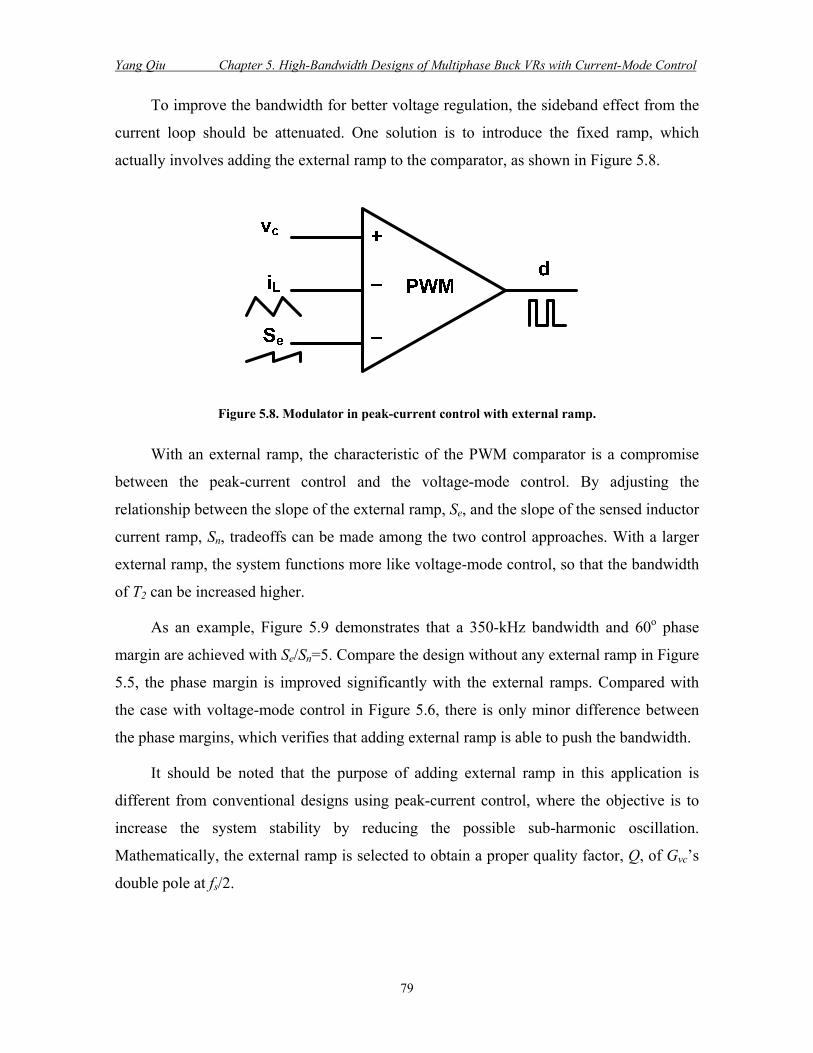
Yang Qiu Chapter 5. High-Bandwidth Designs of Multiphase Buck VRs with Current-Mode Control
To improve the bandwidth for better voltage regulation, the sideband effect from the
current loop should be attenuated. One solution is to introduce the fixed ramp, which
actually involves adding the external ramp to the comparator, as shown in Figure 5.8.
Figure 5.8. Modulator in peak-current control with external ramp.
With an external ramp, the characteristic of the PWM comparator is a compromise
between the peak-current control and the voltage-mode control. By adjusting the
relationship between the slope of the external ramp, Se, and the slope of the sensed inductor
current ramp, Sn, tradeoffs can be made among the two control approaches. With a larger
external ramp, the system functions more like voltage-mode control, so that the bandwidth
of T2 can be increased higher.
As an example, Figure 5.9 demonstrates that a 350-kHz bandwidth and 60o phase
margin are achieved with Se/Sn=5. Compare the design without any external ramp in Figure
5.5, the phase margin is improved significantly with the external ramps. Compared with
the case with voltage-mode control in Figure 5.6, there is only minor difference between
the phase margins, which verifies that adding external ramp is able to push the bandwidth.
It should be noted that the purpose of adding external ramp in this application is
different from conventional designs using peak-current control, where the objective is to
increase the system stability by reducing the possible sub-harmonic oscillation.
Mathematically, the external ramp is selected to obtain a proper quality factor, Q, of Gvc’s
double pole at fs/2.
79

Yang Qiu Chapter 5. High-Bandwidth Designs of Multiphase Buck VRs with Current-Mode Control
1 . 103 1 . 104 1 . 105 1 . 10640
20
0
20
40
60
1 . 103 1 . 104 1 . 105 1 . 106270
180
90
0
Frequency (Hz)
Phas
e (o
)M
agni
tude
(dB
)
fs=1MHz
fc=350kHz
φm=60o
Figure 5.9. Loop gain, T2, of the 1-MHz 2-phase buck converter with peak-current control, Se/Sn=5.
In a typical design where the sub-harmonic oscillation is a concern, the external ramp
is added so that the Q value is around one as a tradeoff between the stability and dynamic
performance. Because
)5.0)1((
1
−−⋅+
=D
SSS
Q
n
neπ,
(5.1)
with small duty cycles in the VR application, Q value is very low even without an external
ramp. For example, a buck converter with 12-V input and 1.2-V output has Q of 0.8 when
Se=0. With a large external ramp, there is a very small Q. Figure 5.10 illustrates Q as a
function of Se/Sn. To achieve more benefit of reducing the influence of the sideband effect
in the current loop, it is desired to add external ramps as more as possible. Hence, Q=1 is
no longer a good practice for this application.
80

Yang Qiu Chapter 5. High-Bandwidth Designs of Multiphase Buck VRs with Current-Mode Control
0 2 4 6 8 10
0.2
0.4
0.6
0.8
1
0
Se/Sn
Q
0 2 4 6 8 10
0.2
0.4
0.6
0.8
1
0
Se/Sn
Q
Figure 5.10. Q value of the fs/2 double pole as a function of Se/Sn for a 12-V-to-1.2-V buck converter.
However, if the external ramp overwhelms the inductor current information, the
peak-current control becomes similar to the voltage-mode control. Under this
circumstance, there is insignificant function on current sharing control among the phases.
Therefore, one has to make the tradeoff between the current sharing performance and
voltage regulation. This is related to another research topic being carried on in the VRM
group in CPES and is not discussed here.
5.3 Bandwidth Improvement with Inductor Current Coupling
As shown in Figure 5.3, with interleaving technique, the sideband effect of fp-fs at Vo
is cancelled because it includes the switching information for all the paralleled phases. In
the current loop, the paralleled phases cannot use the total current information, because
otherwise the current sharing cannot be achieved. Therefore, the sideband components
appear in the current loop.
However, it is noticed that the inductor current sideband component is out of phase in
Figure 5.3. Therefore, if part of other phases’ current information is utilized in the current
loop of one phase, certain cancellation of the sideband component in the current loop can be
achieved, while current sharing is still maintained.
One possible implementation is coupling the phase currents through the feedback
control, as show in Figure 5.11, where k is the coefficient reflecting the coupling between
81

Yang Qiu Chapter 5. High-Bandwidth Designs of Multiphase Buck VRs with Current-Mode Control
the two phases. The other implementation is through the power stage by using the coupled-
inductor structure, as in Figure 5.12 [53]. For symmetrical phases, the mutual inductance is
21 LLM αα == . (5.2)
where α is the coupling coefficient.
Figure 5.11. Phase-current-coupling control for a 2-phase buck converter.
Figure 5.12. A 2-phase coupled-inductor buck converter.
With these two methods, the PWM ramp waveforms contain the components at twice
the switching frequency. As an example, Figure 5.13 illustrates the inputs of the PWM
82

Yang Qiu Chapter 5. High-Bandwidth Designs of Multiphase Buck VRs with Current-Mode Control
comparator for the two methods for k=α=0.5 with the voltage-loop open. Clearly, the 2fs
information is introduced and the fs information is reduced in each phase’s current loop.
The relationships between the fs ripple and 2fs ripple are identical for the two cases. The
only difference is the magnitude of the ripples. Consequently, for the transfer function of
Gvc, the two cases have identical phase response, as shown in Figure 5.14, and there is only
a gain difference between their magnitude responses. Furthermore, with a stronger
coupling, i.e. larger values of k or α, there is less phase delay at the high-frequency region.
time/µSecs 1µSecs/div
0 1 2 3 4 5
V
2.052.1
2.152.2
2.252.3
2.352.4
Vc
Vramp1, Vramp2
(a) Using phase-current-coupling control, k=0.5.
time/µSecs 1µSecs/div
0 1 2 3 4 5
V
1.3
1.4
1.5
1.6
1.7Vc
Vramp1, Vramp2
(b) Using coupled-inductor structure, α=0.5.
Figure 5.13. Waveforms of the PWM comparator inputs with inductor current information
coupling for 2-phase buck converters.
83

Yang Qiu Chapter 5. High-Bandwidth Designs of Multiphase Buck VRs with Current-Mode Control
100 1 .103 1 .104 1 .105 1 .10680
60
40
20
0
100 1 .103 1 .104 1 .105 1 .106270
180
90
0
Frequency (Hz)
Phas
e (o
)M
agni
tude
(dB
) fs=1MHz
(a) Using phase-current-coupling control. (Red solid line: k=0.5; Blue dotted line: k=0.8).
100 1 .103 1 .104 1 .105 1 .10680
60
40
20
0
100 1 .103 1 .104 1 .105 1 .106270
180
90
0
Frequency (Hz)
Phas
e (o
)M
agni
tude
(dB
) fs=1MHz
(b) Using coupled-inductor structure. (Red solid line: α=0.5; Blue dotted line: α=0.8).
Figure 5.14. Simulated Gvc with inductor current information coupling for 2-phase buck converters.
84

Yang Qiu Chapter 5. High-Bandwidth Designs of Multiphase Buck VRs with Current-Mode Control
Comparing the two methods of coupling schemes, they have similar frequency-
domain responses. From the power-stage aspect, the coupled-inductor design has
additional advantages such as the smaller inductor current ripples [53], which leads to less
switching loss and conduction loss in the converter. Therefore, the following discussion is
based on coupled-inductor buck converters.
To investigate the influence from the coupling effect and thus to develop design
guidelines for the phase-current-coupling control and the coupled-inductor structures, a
small-signal model should be derived. Because the benefit of reducing phase delay is from
cancelling the sideband components around the switching frequency, the model should be
valid at high frequency. However, as mentioned above, it is not simple to extend the multi-
frequency model to the peak-current control. From an equivalent circuit using center-tapped
transformers, an approach similar to the sample-data model has been derived for the
coupled inductor buck converter [54][55]. However, this model is not derived directly from
the original topology, which makes it hard to understand the insight with coupled inductors.
In addition, it is difficult to extend to cases with a phase number larger than two. In this
section, the modeling for the coupled-inductor buck converter is improved.
For simplicity, a 2-phase case is studied first, which is shown in Figure 5.12. The self
inductances of the two inductors’ are L, and their mutual inductance is M. With current
sensing gains of Ri, the input waveforms of the modulator is illustrated in Figure 5.15.
IL1
Vc
Sn Sf Sr
IL2
Vc
kTs/2 (k+2)Ts/2(k+1)Ts/2
Vpp
Figure 5.15. Input waveforms of the PWM comparators in a 2-phase coupled-inductor buck converter.
85

Yang Qiu Chapter 5. High-Bandwidth Designs of Multiphase Buck VRs with Current-Mode Control
The slew rates of the sensed currents are
1eq
oinin L
VVRS −⋅= , (5.3)
2eq
oif L
VRS ⋅= , (5.4)
3eq
oir L
VRS −⋅= , (5.5)
where [53]
LDD
Leq ⋅−−
='/1
)1( 2
1 αα , (5.6)
LLeq ⋅−= )1(2 α , (5.7)
LDD
Leq ⋅−−
=/'1)1( 2
3 αα . (5.8)
D is the duty cycle and
DD −=1' . (5.9)
In the derivation, it is assumed that with modifications of the sample-hold effect, He,
and the PWM gain, Fm, the equivalent single-phase block diagram for the non-coupled
buck converter, as shown in Figure 5.16, is still suitable for the coupling cases, while in the
current loop, the coupling effect is included.
It is derived based on the PWM comparator’s input waveforms in Figure 5.15, the
gain of the comparator is
snm TS
F 1= , (5.10)
Same as the non-coupled case, the equivalent sensing gain
2/iie RR = . (5.11)
86

Yang Qiu Chapter 5. High-Bandwidth Designs of Multiphase Buck VRs with Current-Mode Control
Figure 5.16. System block diagram of the coupled-inductor buck converter with voltage-loop open.
To calculate He, the natural response of one phase’s current, the forced response from
the other phases’ currents perturbations and the control-voltage perturbation need to be
derived and are derived.
The first phase’s current, IL1, with a small-signal variation at kTs/2 is shown in Figure
5.17. The natural response for the next sampling instant at (k+2)Ts/2 is calculated as
)(ˆ)2(ˆ11 ki
SS
ki Ln
fL ⋅−=+ . (5.12)
IL1
Vc
Sn Sf Sr
kTs/2 (k+2)Ts/2(k+1)Ts/2
iL1^
Figure 5.17. Natural response of the phase current, IL1.
87

Yang Qiu Chapter 5. High-Bandwidth Designs of Multiphase Buck VRs with Current-Mode Control
Meanwhile, because IL1’s variation is a result of the duty cycle change, it leads to IL2’s
variation as well. From Figure 5.18, it can be derived that
)(ˆ)1(ˆ12 ki
SSS
ki Ln
frL ⋅
+−=+ . (5.13)
IL1
Vc
kTs/2 (k+1)Ts/2
iL2^
IL2
Figure 5.18. Forced response of IL2 as a result of IL1 variation.
Similarly,
)1(ˆ)3(ˆ22 +⋅−=+ ki
SS
ki Ln
fL . (5.14)
and
)1(ˆ)2(ˆ21 +⋅
+−=+ ki
SSS
ki Ln
frL . (5.15)
Figure 5.19 illustrates the currents’ response when there is the control-voltage
perturbation.
88

Yang Qiu Chapter 5. High-Bandwidth Designs of Multiphase Buck VRs with Current-Mode Control
Figure 5.19. Forced responses of IL1 and IL2 as results of Vc variation.
It is derived that
)(ˆ1)(ˆ1 kv
RSSS
ki cin
fnL ⋅⋅
+= , (5.16)
and
)(ˆ1)(ˆ2 kv
RSSS
ki cin
frL ⋅⋅
+= , (5.17)
Similarly, it is obtained that
)1(ˆ1)1(ˆ2 +⋅⋅
+=+ kv
RSSS
ki cin
fnL , (5.18)
)1(ˆ1)1(ˆ1 +⋅⋅
+=+ kv
RSSS
ki cin
frL , (5.19)
Based on (5.3)~(5.8), the relationship between Sn, Sr, and Sf is expressed as
)( fnfr SSSS +⋅=+ α . (5.20)
89

Yang Qiu Chapter 5. High-Bandwidth Designs of Multiphase Buck VRs with Current-Mode Control
Therefore,
).(ˆ)1(ˆ)2(ˆ12
1
)2(ˆ
12
1
kiSS
kiS
SSkv
RSSS
ki
Ln
fL
n
fnc
in
fn
L
⋅−+⋅+
⋅−+⋅⋅+
⋅+
=
+
αα (5.21)
The z-transform of (5.21) is given by
).(ˆ)(ˆ)(ˆ12
1)(ˆ
12
21
1
ziSS
zziS
SSzzv
RSSS
zi
Ln
fL
n
fnc
in
fn
L
⋅⋅−⋅+
⋅⋅−⋅⋅+
⋅+
= −− αα (5.22)
For symmetrical phases,
)(ˆ)(ˆ21 zizi LL = (5.23)
Therefore,
n
f
n
fn
in
fn
c
L
c
L
SS
zS
SSz
RSSS
zvzi
zvzizH
⋅++
⋅⋅+
⋅+
⋅+
===−− 21
21
1
12
1
)(ˆ)(ˆ
)(ˆ)(ˆ
)(α
α
(5.24)
Transform to the s-domain, it is
s
sT
i
n
fsT
n
fnsT
n
fn
c
L
sTe
RSS
eS
SSe
SSS
svsi s
ss
1121
)(ˆ)(ˆ
2/
1 −⋅⋅
+⋅+
⋅+
+⋅
+
=α
α
(5.25)
On the other hand, from Figure 5.16, the transfer function is derived as
eieim
im
c
L
HRFFFF
svsi
+=
1)(ˆ)(ˆ
1 . (5.26)
Since an equivalent single-phase buck converter model is used, the transfer functions in
Figure 5.16 are using the equivalent inductor, whose value is equal to the paralleled two
phases’ transient inductance,
90

Yang Qiu Chapter 5. High-Bandwidth Designs of Multiphase Buck VRs with Current-Mode Control
2)1(
22 LL
L eqeq
α−== . (5.27)
Assuming constant input and output voltage,
).(122)(ˆ
)(ˆ)(ˆ
2
21fn
ieq
inLLi SS
sRsLV
sdsisiF +
+⋅=⋅=
+=
α (5.28)
Combining (5.10), (5.20), (5.25), (5.26), and (5.28), it is obtained that
α
αα
+−
⋅+−
⋅−=
11
2/21
)1()(
2/ss sTs
sTs
eesT
esT
sH . (5.29)
To prove the derived model, Figure 5.20 compares the simulated and calculated Gvc
transfer functions for a 2-phase coupled-inductor buck converter. For both the coupling
coefficients of 0.5 and 0.8, the model predicts the performance very well up to the
switching frequency.
Extending to an n-phase coupled-inductor buck converter, it is obtained using the
same approach that
α
αα
+−
⋅+−
⋅−−=
11
/1
))1(1()(
/ nsTs
sTs
e
ss ensTn
esTn
sH , (5.30)
where α is the coupling coefficient between either two phases.
Mathematically, the sample-hold effect, He, can be used to represent the influence
from the switching frequency. The reason for phase response improvement with coupled
inductors can be clearly indicated in (5.29) and (5.30). With the 2-phase coupled-inductor
structure, the sample-hold effect at fs is reduced when the 2fs sampling is introduced. When
there is no coupling, i.e. α=0, it is exactly the same as conventional buck converters. With a
higher coupling coefficient, there is smaller sample-hold effect at fs, while larger sample-
hold effect at fs/2.
91

Yang Qiu Chapter 5. High-Bandwidth Designs of Multiphase Buck VRs with Current-Mode Control
100 1 .103 1 . 104 1 .105 1 .10680
60
40
20
0
20
100 1 .103 1 . 104 1 .105 1 .1062702251801359045
045
Frequency (Hz)
Phas
e (o
)M
agni
tude
(dB
) fs=1MHz
(a) SIMPLIS simulation result. (Red solid line: α=0.5; Blue dotted line: α=0.8)
100 1 .103 1 .104 1 .105 1 .10680
60
40
20
0
20
100 1 .103 1 .104 1 .105 1 .1062702251801359045
045
Frequency (Hz)
Phas
e (o
)M
agni
tude
(dB
) fs=1MHz
(b) Modeling result. (Red solid line: α=0.5; Blue dotted line: α=0.8)
Figure 5.20. Gvc transfer functions of a 2-phase coupled-inductor buck converter.
92

Yang Qiu Chapter 5. High-Bandwidth Designs of Multiphase Buck VRs with Current-Mode Control
Figure 5.21 illustrates the influence of He with different coupling coefficient. For non-
couple cases, the influence from He can be explained as a pair of right-half-plane (RHP)
zeroes, which leads to magnitude increase and phase delays. With coupling introduced,
there are less magnitude and phase delays near the switching frequency, which means the
sample-hold effect at fs is attenuated. Therefore, when the coupling coefficient is high
enough, it is possible to push the bandwidth higher.
1 .103 1 .104 1 .105 1 .10620
0
20
40
1 .103 1 .104 1 .105 1 .106180
90
0
90
Frequency (Hz)
Phas
e (o
)M
agni
tude
(dB
)
fs=1MHz
Figure 5.21. Sample-hold effect in the coupled-inductor buck converters.
(Red solid line: α=0; Blue dashed line: α=0.5; Brown dotted line: α=0.8)
As a design example, for a 1-MHz 2-phase coupled-buck converter with α=0.8, its T2
loop gain achieves 350-kHz with 60o phase margin, as shown in Figure 5.22. To verify the
analysis, a prototype of a 1-MHz 4-phase buck converter is built with coupled inductors.
Because of the simple structure of coupling two phases, the circuit in Figure 5.23 is used,
where the first and second phases have 180o phase shift with the 2-phase inductor coupling.
The coupling coefficient is 0.8. The third and fourth phases are also coupled. Meanwhile,
they have 90o phase shift from the first two phases. With this prototype, Figure 5.24
compares T2 loop gain of the non-coupled case with the coupled case.
93

Yang Qiu Chapter 5. High-Bandwidth Designs of Multiphase Buck VRs with Current-Mode Control
1 . 103 1 . 104 1 . 105 1 . 10640
20
0
20
40
60
1 . 103 1 . 104 1 . 105 1 . 106270
180
90
0
Frequency (Hz)
Phas
e (o
)M
agni
tude
(dB
)
fs=1MHz
fc=350kHz
φm=60o
Figure 5.22. Simulated T2 loop gain of a 2-phase coupled-inductor buck converter with α=0.8.
Figure 5.23. A 4-phase buck converter with 2-phase coupled-inductor design.
94

Yang Qiu Chapter 5. High-Bandwidth Designs of Multiphase Buck VRs with Current-Mode Control
100 1 . 103 1 . 104 1 . 105 1 . 10640
20
0
20
40
60
100 1 . 103 1 . 104 1 . 105 1 . 106360
270
180
90
0
90
Frequency (Hz)
Phas
e (o
)M
agni
tude
(dB
)
fs=1MHz
fc=180kHz
φm=60o
(a) Without coupling (α=0), fc=180kHz.
100 1 . 103 1 . 104 1 . 105 1 . 10640
20
0
20
40
60
100 1 . 103 1 . 104 1 . 105 1 . 106360
270
180
90
0
90
Frequency (Hz)
Phas
e (o
)M
agni
tude
(dB
)
fs=1MHz
fc=350kHz
φm=60o
(b) With coupling (α=0.8), fc=350kHz.
Figure 5.24. T2’s loop gain of a 1-MHz 4-phase buck converter with 2-phase coupling.
95

Yang Qiu Chapter 5. High-Bandwidth Designs of Multiphase Buck VRs with Current-Mode Control
With coupled inductors, the bandwidth is pushed from 180 kHz, i.e. fs/6, to 350 kHz,
which is around fs/3 with the same phase margin of 60o. According to the previous analysis,
the phase drop at fs still exists in the coupled case because the sample-hold function at fs
cannot be totally eliminated.
5.4 Summary
In this chapter, the influence on the voltage regulation loop bandwidth from the peak-
current control loop is studied. Because the inductor current is fed back for each phase, the
sideband effect cannot be cancelled in the multiphase buck converters. Excessive
magnitude and phase delays are observed in the loop gain.
To increase the bandwidth, the sideband effect in the current loop needs to be
reduced. One solution is to weaken the current loop’s influence with external ramps to the
modulator. With a weak current loop, a faster voltage regulation loop can be achieved.
This chapter also studies another method of increasing the bandwidth by increasing
the effective switching frequency with coupling the inductor current information, which
can be realized either by coupling the phase current through feedback or using the coupled-
inductor structure in the power stage. The derived sample-data model indicates that the fs
information is reduced with coupling. Consequently, the phase delay is decreased and the
high-bandwidth design is obtained. To verify the analysis, a 1-MHz prototype is built and a
bandwidth of 350 kHz is achieved with a 60o phase margin.
96

Chapter 6. Conclusions
6.1 Summary
Future microprocessor poses many challenges to the VRs, such as the low voltage,
high current, fast load transient, etc. In VR designs using multiphase buck converters, one
of the results from these stringent challenges is a large amount of output capacitors, which
is undesired from both the cost and the motherboard real estate aspects. In order to save the
output capacitors, the control-loop bandwidth must be increased. However, the bandwidth
is limited in the practical design. The influence from the switching frequency on the
control-loop bandwidth has not been identified, and the influence from multiphase is not
clear, either. Since the widely-used average model eliminates the inherent switching
functions, it is not able to predict the converter’s high-frequency performance. In this
dissertation, the primary objectives are to develop the methodology of high-frequency
modeling for the buck and multiphase buck converters, and to analyze their high-frequency
characteristics.
First, the nonlinearity of the PWM scheme is identified. Because of the sampling
characteristic, the sideband components are generated at the output of the PWM
comparator. With the assumption that the low-pass filters in the converter well attenuate
the sideband components, the conventional average model only includes the perturbation-
frequency components. When studying the high-frequency performance, the lowest
sideband frequency is not high enough as compared with the perturbation one; therefore,
the assumption for the average model is not good any more. Under this condition, the
converter response cannot be reflected by the average model. Furthermore, with a closed
loop, the generated sideband components at the output voltage appear at the input of the
PWM comparator, and then generate the perturbation frequency at the output, too. This
causes the sideband effect to happen. The perturbation-frequency components and the
sideband components are coupled through the comparator. To be able to predict the
converter’s high-frequency performance, it is necessary to have a model that reflects the
sampling characteristic of the PWM comparator. As the basis of further research, the
97

Yang Qiu Chapter 6. Conclusions
existing high-frequency modeling approaches are reviewed. Among them, the harmonic
balance approach predicts the high-frequency performance but it is too complicated to
utilize. However, it is promising when simplified in the applications with buck and
multiphase buck converters. Once the nonlinearity of the PWM comparator is identified, a
simple model can be obtained because the rest of the converter system is a linear function.
With the Fourier analysis, the relationship between the sideband components and the
perturbation-frequency components are derived for the trailing-edge PWM comparator.
The concept of multi-frequency modeling is developed based on a single-phase voltage-
mode-controlled buck converter. The system stability and transient performance depend on
the loop gain that is affected by the sideband component. From the multi-frequency model,
it is mathematically indicated that the result from the sideband effect is the reduction of
magnitude and phase characteristics of the loop gain. With a higher bandwidth, there are
more magnitude and phase reductions, which cause the sideband effect to pose limitations
when pushing the bandwidth.
The proposed model is then applied to the multiphase buck converter. For voltage-
mode control, the multiphase technique has the potential to cancel the sideband effect
around the switching frequency. Therefore, theoretically the control-loop bandwidth can be
pushed higher than the single-phase design. However, in practical designs, there is still
magnitude and phase reductions around the switching frequency in the measured loop gain.
Using the multi-frequency model, it is clearly pointed out that the sideband effect cannot
be fully cancelled with unsymmetrical phases, which results additional reduction of the
phase margin. Therefore, one should be extremely careful to push the bandwidth when
depending on the interleaving to cancel the sideband effect.
The multiphase buck converter with peak-current control is also investigated.
Because of the current loop in each individual phase, there is the sideband effect that
cannot be canceled with the interleaving technique. For higher bandwidths and better
transient performances, two schemes are presented to reduce the influence from the current
loop: the external ramps are inserted in the modulators, and the inductor currents are
coupled, either through feedback control or by the coupled-inductor structure. A bandwidth
98

Yang Qiu Chapter 6. Conclusions
around one-third of the switching frequency is achieved with the coupled-inductor buck
converter, which makes it a promising circuit for the VR applications.
As a conclusion, the feedback loop results in the sideband effect, which limits the
bandwidth and is not included in the average model. With the proposed multi-frequency
model, the high-frequency performance for the buck and multiphase buck converters can
be accurately predicted.
6.2 Future Works
Most of the research in this dissertation is based on voltage-mode control. The multi-
frequency model, which clearly describes the influences from the sideband components,
has not yet been derived for cases with current loops. The relationship between the multi-
frequency model and the sample-data model has not been clarified. It could be interesting
to extend the modeling work to current-mode control. Meanwhile, it has been proposed to
reduce the influence from the current loop to increase the bandwidth, therefore, there is
tradeoff between the current sharing and voltage regulation. This design tradeoff can be
identified only when the model with current loop is obtained. This exploration could be
another interesting research topic.
99

Appendix A. Analyses with Different PWM Schemes
For the discussions and analysis in this dissertation, the example of trailing-edge type
of PWM comparator is used. The PWM comparator model has not been generalized for
other kinds of modulation schemes, such as the leading-edge and double-edge modulations,
as shown in Figure A.1. There has been interest in how the modulation schemes influences
the control-loop bandwidth, especially for the double-edge modulation [56]. In this
appendix, the extended describing functions for the PWM comparator with different
modulation schemes are derived using the Fourier analysis. The modulation schemes’
influences on the sideband effect and the control-loop bandwidth are compared. The high-
frequency performances are explained using the multi-frequency model.
Vr
vc
Ts
(a) Trailing-edge modulation.
Vr
vc
Ts
(b) Leading-edge modulation.
Vr
vc
Ts
(c) Double-edge modulation.
Figure A.1. Input and output waveform of the PWM comparator with different modulation schemes.
100

Yang Qiu Appendix A. Analyses with Different PWM Schemes
The essence to include the sampling information in the high-frequency model is to
model the PWM comparator. Generally, for constant-frequency controls, the input and
output waveforms of the modulator are shown in Figure A.2. With different ratios between
the rising time, Tr, and the falling time, Tf, the trailing-edge, leading-edge and double-edge
modulations are realized.
In Figure A.2, with given perturbations, the Fourier analysis is performed on the
waveforms of vc and d, using the same approach as in Chapter 3. With calculated Fourier
coefficients of the input and output waveforms, the function of the comparator can be
obtained by comparing their coefficients at different frequencies.
Vr
vc
Tk
Ts
dTr Tf
Figure A.2. Input and output waveforms of the PWM comparator of constant-frequency control.
With a ramp waveform as in Figure A.2 and the peak-to-peak value of VR, for a
control voltage of
)sin(ˆ)( θω −+= tvVtv pccc , (A.1)
with small-signal approximations, the duty ratio for the k-th cycle is
,)])1[(sin(ˆ
)])1[(sin(ˆ
Rs
rfspcr
Rs
ffspcf
s
k
VTDTTTkvT
VTDTTTkvT
DTT
⋅
−++−⋅+
⋅−−+−⋅
+=
θω
θω
(A.2)
where D=Vc/VR, is the DC duty cycle. After going through the similar process as in Chapter
3, the results listed in Table A.1 are obtained for ωp≠kωs/2, k=1, 2, 3, …
101

Yang Qiu Appendix A. Analyses with Different PWM Schemes
Table A.1. Extended describing functions of the PWM comparator with different modulations.
Describing
Functions
Trailing-Edge PWM
(Tf=0)
Leading-Edge PWM
(Tr=0)
Double-Edge PWM
(Tr=Tf)
)()(
ωω
cm v
dF = RV
1 RV
1 RV
1
)()(
pc
spm v
dF
ωωω −
=−
R
jD
Ve π2
R
jD
Ve π2−
RVD )cos( π−
)()(
spc
pm v
dF
ωωω−
=+
R
jD
Ve π2−
R
jD
Ve π2
RVD )cos( π−
Clearly, the describing function of the PWM comparator for the same frequency input
and output is a constant gain for all the three cases. It is not a function of Tr or Tf.
Therefore, for the same input and output frequency, the modulation types do not change
the function of the PWM comparator.
For the extended describing functions between different frequencies, when the duty
cycle changes, the phases change accordingly, while the magnitudes are constant for
trailing-edge and leading-edge modulations. However, for the double-edge modulation, the
magnitude is a function of the duty cycle. Assuming the triangle ramp peak-to-peak
voltage, VR, is 1 V, Figure A.3 illustrates the magnitude of Fm+ and Fm-.
0 0.2 0.4 0.6 0.8 10
0.2
0.4
0.6
0.8
1
|Fm
+| &
|Fm
-|
Duty Cycle0 0.2 0.4 0.6 0.8 10
0.2
0.4
0.6
0.8
1
|Fm
+| &
|Fm
-|
Duty Cycle
Figure A.3. Magnitude of Fm+ and Fm- as a function of the duty cycle for the double-edge modulation.
102
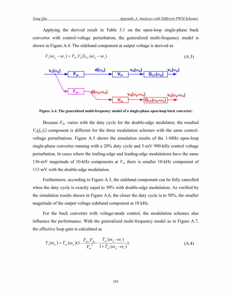
Yang Qiu Appendix A. Analyses with Different PWM Schemes
Applying the derived result in Table 3.1 on the open-loop single-phase buck
converter with control-voltage perturbation, the generalized multi-frequency model is
shown in Figure A.4. The sideband component at output voltage is derived as
)()( spLCinmspo GVFV ωωωω −=− − (A.3)
d(ωp)vc(ωp)Fm
d(ωp-ωs)Fm-
Vin
Vin
vd(ωp)
vd(ωp-ωs)
GLC(ωp)vo(ωp)
vo(ωp-ωs)GLC(ωp-ωs)
Figure A.4. The generalized multi-frequency model of a single-phase open-loop buck converter.
Because Fm- varies with the duty cycle for the double-edge modulator, the resulted
Vo(fp-fs) component is different for the three modulation schemes with the same control-
voltage perturbations. Figure A.5 shows the simulation results of the 1-MHz open-loop
single-phase converter running with a 20% duty cycle and 5-mV 990-kHz control voltage
perturbation. In cases where the trailing-edge and leading-edge modulations have the same
136-mV magnitude of 10-kHz components at Vo, there is smaller 10-kHz component of
113 mV with the double-edge modulation.
Furthermore, according to Figure A.3, the sideband component can be fully cancelled
when the duty cycle is exactly equal to 50% with double-edge modulation. As verified by
the simulation results shown in Figure A.6, the closer the duty cycle is to 50%, the smaller
magnitude of the output voltage sideband component at 10 kHz.
For the buck converter with voltage-mode control, the modulation schemes also
influence the performance. With the generalized multi-frequency model as in Figure A.7,
the effective loop gain is calculated as
).)-(1
)-(-)(1()( 2
spav
spav
m
mmpavpv T
T
FFF
TTωω
ωωωω
+⋅= −+ (A.4)
103

Yang Qiu Appendix A. Analyses with Different PWM Schemes
time/mSecs 100uSecs/div
4.5 4.6 4.7 4.8 4.9
Vo / V
2.152.2
2.252.3
2.352.4
2.452.5
Vo /
V
(a) Trailing-edge modulation.
time/mSecs 100uSecs/div
4.6 4.7 4.8 4.9 5
Vo / V
2.152.2
2.252.3
2.352.4
2.452.5
Vo /
V
time/mSecs 100uSecs/div
4.6 4.7 4.8 4.9 5
Vo / V
2.152.2
2.252.3
2.352.4
2.452.5
Vo /
V
(b) Leading-edge modulation.
time/mSecs 100uSecs/div
4.5 4.6 4.7 4.8 4.9
Vo / V
2.152.2
2.252.3
2.352.4
2.452.5
Vo /
V
(c) Double-edge modulation.
Figure A.5. Simulated Vo waveforms with 20% duty cycle for 1-MHz open-loop buck converters
with 990-kHz Vc perturbations and different modulation schemes.
104

Yang Qiu Appendix A. Analyses with Different PWM Schemes
time/mSecs 100uSecs/div
4.5 4.6 4.7 4.8 4.9
Vo / V
4.454.5
4.554.6
4.654.7
4.754.8
Vo /
V
(a) D=40%.
time/mSecs 100uSecs/div
4.6 4.7 4.8 4.9 5
Vo / V
5.65.655.7
5.755.8
5.855.9
5.95
Vo /
V
(b) D=50%.
Figure A.6. Simulated Vo waveforms for 1-MHz open-loop buck converters with 990-kHz Vc
perturbations and the double-edge modulation.
Figure A.7. The generalized multi-frequency model of a voltage-mode-controlled buck converter.
105

Yang Qiu Appendix A. Analyses with Different PWM Schemes
Since the loop gain’s magnitude and phase reductions around the switching frequency
are caused by the sideband effect represented by the second term, the bandwidth is strongly
dependent on the coupling coefficients of Fm+ and Fm-. From Table 3.1, Fm+·Fm- for the
trailing-edge and leading-edge modulations is independent from the duty cycle, D. However
for the double-edge modulation, it changes with D.
Assuming VR=1, Figure A.8 shows the relative magnitudes of Fm+·Fm- as a function of
the duty cycle. Unlike the other two modulations, the double-edge modulation has the
ability to cancel the sideband effect when the duty cycle is 50%. Consequently, there is less
sideband effect for the double-edge modulations when the duty cycle is close to 50%.
0 0.2 0.4 0.6 0.8 10
0.2
0.4
0.6
0.8
1
1.2
0 0.2 0.4 0.6 0.8 10
0.2
0.4
0.6
0.8
1
1.2
0 0.2 0.4 0.6 0.8 10
0.2
0.4
0.6
0.8
1
1.2
0 0.2 0.4 0.6 0.8 10
0.2
0.4
0.6
0.8
1
1.2
Duty Cycle
F m+*
F m-
Trailing-edge & Leading-edge
Double-edge
Figure A.8. Comparison of the magnitude of sideband effect, Fm+*Fm-, assuming VR=1.
(Red solid line: double-edge modulation; Blue dotted line: trailing-edge and leading-edge modulation.)
As shown in Figure A.9, for the same bandwidth and a 50% duty cycle, more phase
margin is achieved with the double-edge modulation as compared with the trailing-edge and
leading-edge modulations. However, with a small duty cycle of 10%, the cancellation of
the sideband effect is insignificant. This phase margin improvement with the double-edge
modulation is strongly depended on the operation duty cycle. The benefit is maximized
only when the duty cycle is around 50%, however, this is not likely to happen in VR
applications.
106

Yang Qiu Appendix A. Analyses with Different PWM Schemes
100 1 .103 1 .104 1 .105 1 .106604020
0204060
100 1 .103 1 .104 1 .105 1 .1062702251801359045
0
Frequency (Hz)
Phas
e (o
)M
agni
tude
(dB
)
fs=1MHz
fc=400kHz
(a) D=50%.
100 1 .103 1 .104 1 .105 1 .106604020
0204060
100 1 .103 1 .104 1 .105 1 .1062702251801359045
0
Frequency (Hz)
Phas
e (o
)M
agni
tude
(dB
)
fs=1MHz
fc=400kHz
(b) D=10%.
Figure A.9. Loop gain comparison among PWM methods.
(Red solid line: double-edge modulation; Blue dashed line: trailing-edge modulation;
Brown dotted line: leading-edge modulation.)
107

Yang Qiu Appendix A. Analyses with Different PWM Schemes
With 12-V input voltage, most VRs operate with a steady-state duty cycle around 10-
15%. In some applications, such as the two-stage solution or the laptop systems, the duty
cycle might be larger with lower input voltage. However, during the load transient from
the microprocessors, the duty cycle of the VR may be saturated. In the practical design, all
the possible operating conditions should be considered when pushing the bandwidth.
Therefore, the benefit from the double-edge modulation is limited.
In summary, when the duty cycle is around 50%, the double-edge modulation can
cancel the sideband effect for the buck converters. However, the cancellation is
insignificant when the duty cycle is small. Therefore, in practical designs, the advantage is
limited for pushing the control-loop bandwidth.
108

Appendix B. Analyses with Input-Voltage Variations
In the previous discussions, it is assumed that the input voltage of the buck or
multiphase buck converter is constant. The nonlinearity of the switch function has not been
considered. By this way, the function of the switches can be regarded as a simple gain. In
this appendix, the detailed model of the switches is derived considering the influence of the
input-voltage variations.
As an example, the converter with the trailing-edge modulation is considered. For
simplicity, the case for an open-loop buck converter with only the input perturbation is
studied first, as shown in Figure B.1. With only the input-voltage perturbation, the phase
voltage waveform is illustrated as in Figure B.2.
L
vovin
Cfs
vcVr
vd
Rofp d
PWM
Figure B.1. An open-loop buck converter with the input-voltage perturbations.
vin
d
vd
Figure B.2. The phase voltage waveform with the input-voltage perturbation
assuming a constant duty cycle.
109

Yang Qiu Appendix B. Analyses with Input-Voltage Variations
In this case, the nonlinearity exists because of the switches shown in Figure B.3. To
obtain the extended describing functions for the switches, the similar approach of modeling
the PWM comparator using the Fourier analysis is applied.
vin vd
d
Figure B.3. Switches in the converters.
With a sinusoidal input voltage of
)(sinˆ)( θω −+= tvVtv pininin , (B.1)
it is assumed that the perturbation frequency, ωp, and the switching frequency, ωs, have the
relationship of
MN
s
p =ωω
. (B.2)
where N and M are positive integers. Then the Fourier coefficient at ωp for the phase
voltage is expressed as
∑ ∫=
+−
−
−=M
k
DTTk
Tkp
tjinpd
spsp
sp
p tdetvN
v1
)1(
)1(
)()(2
1)(ωω
ω
ω ωπ
ω . (B.3)
It is obtained that when ωp ≠kωs/2, k=1, 2, 3, …,
)()( pinpd Dvv ωω = . (B.4)
Meanwhile,
110

Yang Qiu Appendix B. Analyses with Input-Voltage Variations
∑ ∫=
−+−−
−−
−− −−
=−M
k
DTTk
Tksp
tjinspd
sspssp
ssp
sp tdetvMN
v1
)())(1(
))(1(
)( ))(()()(2
1)(ωωωω
ωω
ωω ωωπ
ωω . (B.5)
It is derived that when ωp ≠kωs/2, k=1, 2, 3, …,
)(2
1)(2
pin
Dj
spd vj
ev ωπ
ωωπ −
=− , (B.6)
Similarly, it is obtained that
)(2
1)(2
spin
Dj
pd vj
ev ωωπ
ωπ
−−
−=
−
. (B.7)
These extended describing functions are summarized in Table B.1. The relationship
between the same frequency input and output components is a simple gain of duty cycle,
which is the same as the result from the average model. The extended describing functions
between different frequencies are illustrated in Figure B.4.
For the case as Figure B.1, the model for the circuit is illustrated in Figure B.5. To
verify the relationship between different frequencies components, the switching-model
simulation with input sinusoidal perturbations are performed. A 999-kHz perturbation is
inserted to the input voltage of a 1-MHz buck converter with 1.2-V output, 80-mΩ load
resistor, 200-nH inductor, and 1-mF capacitor.
Table B.1. Extended describing functions from the input voltage to the phase voltage.
Output components
)( pdv ω )( spdv ωω −
)( pinv ω D π
π
je Dj
212 −
Input
components )( spinv ωω −
π
π
je Dj
212
−−−
D
111
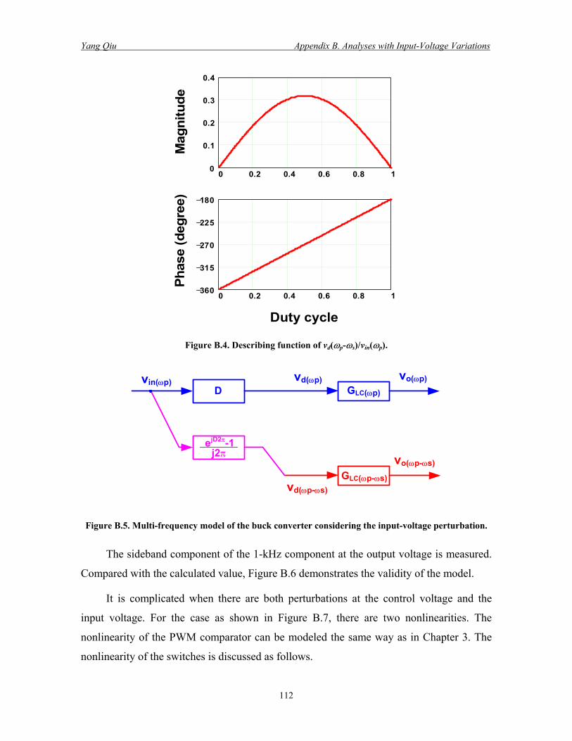
Yang Qiu Appendix B. Analyses with Input-Voltage Variations
0 0.2 0.4 0.6 0.8 10
0.1
0.2
0.3
0.4
0 0.2 0.4 0.6 0.8 1360
315
270
225
180
Mag
nitu
dePh
ase
(deg
ree)
Duty cycle
Figure B.4. Describing function of vd(ωp-ωs)/vin(ωp).
vd(ωp)vin(ωp)D
vd(ωp-ωs)
ejD2π-1j2π
GLC(ωp)
GLC(ωp-ωs)
vo(ωp)
vo(ωp-ωs)
Figure B.5. Multi-frequency model of the buck converter considering the input-voltage perturbation.
The sideband component of the 1-kHz component at the output voltage is measured.
Compared with the calculated value, Figure B.6 demonstrates the validity of the model.
It is complicated when there are both perturbations at the control voltage and the
input voltage. For the case as shown in Figure B.7, there are two nonlinearities. The
nonlinearity of the PWM comparator can be modeled the same way as in Chapter 3. The
nonlinearity of the switches is discussed as follows.
112

Yang Qiu Appendix B. Analyses with Input-Voltage Variations
0 0.2 0.4 0.6 0.8 10
0.1
0.2
0.3
0.4
Duty cycle
|vo(ω
p-ω
s)/v
in(ω
p)|
0 0.2 0.4 0.6 0.8 10
0.1
0.2
0.3
0.4
Duty cycle
|vo(ω
p-ω
s)/v
in(ω
p)|
Figure B.6. Comparison between the simulation and modeling with the input-voltage perturbation.
(Red solid line: prediction using multi-frequency model; Blue dots: switching-model simulation results.)
L
vovin
Cfs
fp
vcvR
vd
Rofp d
PWM
Figure B.7. Buck converter with perturbations at both the control voltage and input voltage.
vin
d
vd
Figure B.8. Function of the switches in the buck converters.
As shown in Figure B.8, the function of the switches is
)()( tvtv ind = when , 1)( =td (B.8)
113

Yang Qiu Appendix B. Analyses with Input-Voltage Variations
0)( =tvd when . 0)( =td (B.9)
Therefore, the phase voltage can be expressed by
)()()( tvtdtv ind ⋅= . (B.10)
In the frequency domain, the relationship is represented by the convolution,
)()()( ωωω ind vdv ⊗= . (B.11)
It is rewritten as
...)0()()()0()( +⋅+⋅= inppinpd vdvdv ωωω . (B.12)
With small signal assumption, the higher order components are ignored. Therefore, it
is obtained that
inppinpd VdvDv ⋅+⋅= )()()( ωωω , (B.13)
and
inspspinspd VdvDv ⋅−+−⋅=− )()()( ωωωωωω . (B.14)
Therefore, the super-positioning can be used to address perturbations from both the
input voltage and control voltage. With (B.14), the multi-frequency model including the
nonlinearities of both the PWM comparator and the switches is illustrated in Figure B.9.
d(ωp)vc(ωp) 1/Vr
vc(ωp-ωs)
+1/Vr d(ωp-ωs)
+
+
ejD2π/Vr
+e-jD2π/Vr
Vinvd(ωp)
D
vin(ωp)
ejD2π-1j2π
vd(ωp-ωs)
+ +
++
Vin
Figure B.9. Multi-frequency model of the nonlinearities of the buck converter.
114

Yang Qiu Appendix B. Analyses with Input-Voltage Variations
Based on the previous analysis, a voltage-mode-controlled buck converter with the
input-voltage perturbation is modeled, as in Figure B.10. It is derived that the audio-
susceptibility considering the sideband effect is
)()(1
)()(2
1
)(1)(
1
)()()(
2
spavpav
spavpLC
jD
spav
pav
pLC
pc
po
TT
TGj
e
TTGD
vv
ωωω
ωωωπ
ωωωω
ωω
π
−++
−⋅⋅−
+
−++
⋅=
−
. (B.15)
d(ωp)vc(ωp) 1/Vr
vc(ωp-ωs)
+1/Vrd(ωp-ωs)
+
+
ejD2π/Vr
+e-jD2π/Vr
Vin
Vin
vd(ωp)
vd(ωp-ωs)
GLC(ωp)
GLC(ωp-ωs)
vo(ωp)
vo(ωp-ωs)
-Hv(ωp-ωs)
-Hv(ωp)
D
vin(ωp)
ejD2π-1
+ +
+ +j2π
Figure B.10. Multi-frequency model of a voltage-mode-controlled buck converter
with the input-voltage perturbation.
The comparison of the closed-loop audio-susceptibility is shown in Figure B.11.
Clearly, the average model is accurate compared with the simulation result in the low-
frequency range. However, because of the existing sideband effect, the high-frequency
performance can only be predicted by the multi-frequency model.
115

Yang Qiu Appendix B. Analyses with Input-Voltage Variations
10 100 1 . 103 1 . 104 1 . 105 1 . 106100
80
60
40
20
10 100 1 . 103 1 . 104 1 . 105 1 . 106180
90
0
90
Frequency (Hz)
Phas
e (o
)M
agni
tude
(dB
) fs=1MHz
(a) D=10%.
10 100 1 . 103 1 . 104 1 . 105 1 . 106100
80
60
40
20
10 100 1 . 103 1 . 104 1 . 105 1 . 106180
90
0
90
Frequency (Hz)
Phas
e (o
)M
agni
tude
(dB
) fs=1MHz
(b) D=40%.
Figure B.11. Comparison of the closed-loop audio-susceptibility.
(Red solid line: SIMPLIS simulation result; Blue dashed line: average-model result; Brown dotted
line: multi-frequency model result)
116

References
[1] R. Hiremane, “From Moore’s Law to Intel Innovation—Prediction to Reality,”
Technology@Intel Magazine, April 2005.
[2] D. P. Jajeh, “Intel Accelerates in A New Direction,” Circuit Posted, November 2004.
[3] Intel Corporation, “Platform 2015: Intel Processor and Platform Evolution for the
Next Decade,” Intel White Paper, March 2005.
[4] B. Crepps, “Building the Multi Building the Multi-Core Future: Power Efficient
Architecture,” Intel Developer Forum, August 2005.
[5] E. Stanford, “New Processors Will Require New Powering Technologies,” Magazine
of Power Electronics Technology, Feburary 2002, pp. 32-42.
[6] E. Stanford, “Microprocessor Roadmap,” Intel Power Summit, August 2005.
[7] A. Rozman, and K. Fellhoelter, “Circuit Considerations for Fast Sensitive, Low-
Voltage Loads in a Distributed Power System,” IEEE APEC, 1995, pp. 33-42.
[8] M. Zhang, M. Jovanovic, and F. C. Lee, “Design Considerations for Low-Voltage
On-board DC/DC Modules for Next Generations of Data Processing Circuits”, IEEE
Transactions on Power Electronics, March 1996, pp. 328-337.
[9] F. Goodenough, “Advanced Microprocessors Demand Amperes of Current at <2V,”
Electronic Design, January 20th, 1997.
[10] X. Zhou, X. Zhang, J. Liu, P.-L. Wong, J. Chen, H. Wu, L. Amoroso, F. C. Lee, and
D. Chen, “Investigation of Candidate VRM Topologies for Future Microprocessors,”
IEEE APEC, 1998, pp. 145-150.
[11] X. Zhou, P.-L. Wong, R. Watson, L. Amoroso, X. Sun, H. Wu, P. Xu, B. Yang, W.
Chen, M. Donati, F. C. Lee and A. Q. Huang, “Voltage Regulator Module for Future
Generation of Processors,” VPEC Annual Seminar Tutorial, 1998.
[12] X. Zhou, “Low-Voltage High-Efficiency Fast-Transient Voltage Regulator Module,”
Ph.D Dissertation, Virginia Tech, Blacksburg, VA, July 1999.
117

Yang Qiu References
[13] P. Xu, X. Zhou, P.-L. Wong, K. Yao, and F. C. Lee, “Design and Performance
Evaluation of Multi-Channel Interleaving Quasi-Square-Wave Buck Voltage
Regulator Module,” HFPC, 2000, pp. 82-88.
[14] Intel Corporation, “Voltage Regulator-Down (VRD) 10.1 Design Guide for Desktop
LGA775 Socket,” Intel Design Guides, April 2005.
[15] Y. Ren, K. Yao, M. Xu, and F. C. Lee, “Analysis of the Power Delivery Path from
the 12-V VR to the Microprocessor,” IEEE Transactions on Power Electronics,
November 2004, pp. 1507-1514.
[16] Y. Ren, “High Frequency, High Efficiency Two-Stage Approach for Future
Microprocessors,” Ph.D Dissertation, Virginia Tech, Blacksburg, VA, April 2005.
[17] L. Amoroso, M. Donati, X. Zhou, and F. C. Lee, “Single Shot Transient Suppressor
(SSTS) for High Current High Slew Rate Microprocessor,” IEEE APEC, 1999, pp.
284-288.
[18] A. M. Wu, and S. R. Sanders, “An Active Clamp Circuit for Voltage Regulation
Module (VRM) Applications,” IEEE Transactions on Power Electronics, September
2001, pp. 623-634.
[19] A. Barrado, R. Vazquez, E. Olias, A. Lazaro, and J. Pleite, “Theoretical Study and
Implementation of a Fast Transient Response Hybrid Power Supply,” IEEE
Transactions on Power Electronics, July 2004, pp. 1003-1009.
[20] Y. Ren, A. Schmit, M. Xu, F. C. Lee, A. Sharma, X. Wu, and K. D. Ngo, “Hybrid
Power Filter with Output Impedance Control,” IEEE PESC, 2005, pp. 1434-1440.
[21] K. Yao, K. Lee, M. Xu, and F. C. Lee, “Optimal Design of the Active Droop Control
Method for the Transient Response,” IEEE APEC, 2003, pp.718-723.
[22] P.-L. Wong, F. C. Lee, P. Xu, and K. Yao, “Critical Inductance in Voltage Regulator
Modules,” IEEE Transactions on Power Electronics, July 2002, pp. 485-492.
[23] P.-L. Wong, “Performance Improvements of Multi-Channel Interleaving Voltage
Regulator Modules with Integrated Coupling Inductors,” Ph.D Dissertation, Virginia
Tech, Blacksburg, VA, March 2001.
118

Yang Qiu References
[24] K. Yao, M. Xu, Y. Meng, and F. C. Lee, “Design Considerations for VRM Transient
Response Based on the Output Impedance,” IEEE Transactions on Power
Electronics, November 2003, pp. 1270-1277.
[25] K. Yao, “High-Frequency and High-Performance VRM Design for the Next
Generations of Processors,” Ph.D Dissertation, Virginia Tech, Blacksburg, VA,
April 2004.
[26] G. W. Wester, and R. D. Middlebrook, “Low-Frequency Characterization of
Switched DC-DC converters,” IEEE Transactions on Aerospace and Electronic
Systems, May 1973, pp. 376-385.
[27] R. D. Middlebrook, and S. Cuk, “A General Unified Approach to Modeling
Switching-Converter Power Stage,” IEEE PESC, 1976, pp. 18-34.
[28] A. R. Brown, and R. D. Middlebrook, “Sampled-Data Modeling of Switching
Regulators,” IEEE PESC, 1981, pp. 349-369.
[29] R. Tymerski, “Frequency Analysis of Time-Interval-Modulated Switched
Networks,” IEEE Transactions on Power Electronics, April 1991, pp. 287-295.
[30] R. Tymerski, “Application of the Time Varying Transfer Function for Exact Small-
Signal Analysis,” IEEE Transactions on Power Electronics, March 1994, pp. 196-
205.
[31] D. J. Perreault, and G. C. Verghese, “Time-Varying Effects and Averaging Issues in
Models for Current-Mode Control,” IEEE Transactions on Power Electronics, May
1997, pp. 453-461.
[32] V. J. Thottuvelil, and G. C. Verghese, “Simulation-Based Exploration of Aliasing
Effects in PWM Power Converters,” IEEE Workshop on Computers in Power
Electronics, 1998, pp. 19-22.
[33] G. C. Verghese, and V. J. Thottuvelil, “Aliasing Effects in PWM Power Converters,”
IEEE PESC, 1999, pp. 1043-1049.
119

Yang Qiu References
[34] R. D. Middlebrook, “Describing Function Properties of a Magnetic Pulse-Width
Modulator,” IEEE Transactions on Aerospace & Electronic Systems, May 1973, pp.
386-398.
[35] Hewlett-Packard Company, Operating and Service Manual for Model 3570A
Network Analyzer, 1977.
[36] J. Groves, “Small Signal Analysis of Nonlinear Systems with Periodic Operating
Trajectories,” Ph.D Dissertation, Virginia Tech, Blacksburg, VA, April 1995.
[37] Transim Technology Corporation, “Power Design Tools,” SIMPLIS Technical
Reference Manual, 1994.
[38] A. R. Brown, and R. D. Middlebrook, “Sampled-Data Modeling of Switching
Regulators,” IEEE PESC, 1981, pp. 349-369.
[39] B. Y. Lau, and R. D. Middlebrook, “Small-Signal Frequency Response Theory for
Piecewise-Constant Two-Switched-Network DC-to-DC Converter Systems,” IEEE
PESC, 1986, pp. 186-200.
[40] G. C. Verghese, C. A. Bruzos, and K. N. Mahabir, “Averaged and Sampled-Data
Models for Current Mode Control: A Re-Examination,” IEEE PESC, 1989, pp. 484-
491.
[41] R. B. Ridley, “A New, Continuous-Time Model for Current-Mode Control,” IEEE
Transactions on Power Electronics, April 1991, pp. 271-280.
[42] E. X. Yang, F. C. Lee, and M. M. Jovanovic, “Small-Signal Modeling of Power
Electronic Circuits Using Extended Describing Function Technique,” VPES
Seminar, 1991, pp. 167-178.
[43] E. X. Yang, F. C. Lee, and M. M. Jovanovic, “Small-Signal Modeling of Series and
Parallel Resonant Converters,” IEEE APEC, 1992, pp. 785-792.
[44] E. X. Yang, F. C. Lee, and M. M. Jovanovic, “Small-Signal Modeling of LCC
Resonant Converter ,” IEEE PESC, 1992, pp. 941-948.
[45] J. Groves, “Small-Signal Analysis Using Harmonic Balance Methods,” IEEE PESC,
1991, pp. 74-79.
120

Yang Qiu References
[46] R. D. Middlebrook, “Predicting Modulator Phase Lag in PWM Converter Feedback
Loops,” Eighth International Solid-State Power Conversion Conference (Powercon
8), 1981, pp. H4.1-H4.6.
[47] Delta Electronics, Power Inductor SPL146 Type Specifications.
[48] Panasonic, Power Choke Coil PCCN6B Specifications.
[49] Linear Technology, “3-Phase Buck Controller for Intel VRM9/VRM10 with Active
Voltage Positioning,” LTC3738 Datasheet, 2004.
[50] Texas Instruments, “High-Frequency, Multiphase Controller,” TPS40090 Datasheet,
2004.
[51] Analog Devices, “6-Bit Programmable 2/3/4-Phase Synchronous Buck Controller,”
ADP3168 Datasheet, 2004.
[52] Maxim, “VRM 9.0, Dual-Phase, Parallelable, Average Current-Mode Controller,”
MAX5037 Datasheet, 2004.
[53] P.-L. Wong, Q. Wu, P. Xu, B. Yang, and F. C. Lee, “Investigating Coupling Inductor
in Interleaving QSW VRM,” IEEE APEC, 2000, pp. 973-978.
[54] J. Zhou, M. Xu, and F. C. Lee, “Small Signal Modeling of a High Bandwidth
Voltage Regulator Using Coupled Inductors,” IEEE PESC, 2005, pp.2790-2796.
[55] J. Zhou, “High Frequency, High Current Density Voltage Regulators,” Ph.D
Dissertation, Virginia Tech, Blacksburg, VA, April 2005.
[56] P. Harriman, “New Control Method Boosts Multiphase Bandwidth,” Power
Electronics Technology, January 2003, pp. 36-45.
121

Vita
The author, Yang Qiu, was born in Beijing, China, in 1976. He received his Bachelor
and Master degrees in Electrical Engineering from Tsinghua University, Beijing, China, in
1998 and 2000, respectively.
Since fall 2000, the author has been working toward the Ph.D. degree in the Center
for Power Electronics Systems (CPES) at Virginia Polytechnic Institute and State
University, Blacksburg, Virginia. His research interests include modeling and control of
converters, high-frequency power conversion, low-voltage high-current conversion
techniques, resonant converters, and distributed power system.
122