high gain adjust range, wideband, voltage … high gain adjust range, wideband and variable gain...
TRANSCRIPT

+5V
-5V
VOUT
VC
0 2V® -
- ®40dB +40dB Gain
VCA810
X1
2
3
V+
V-
1
6
7
5
8
Gain
Adjust
+
Product
Folder
Sample &Buy
Technical
Documents
Tools &
Software
Support &Community
VCA810SBOS275G –JUNE 2003–REVISED DECEMBER 2015
VCA810 High Gain Adjust Range, Wideband and Variable Gain AmplifierOperating from ±5-V supplies, the device gain control1 Featuresvoltage adjusts the gain from –40 dB at a 0-V input to
1• High Gain Adjust Range: ±40 dB 40 dB at a –2-V input. Increasing the control voltage• Differential In, Single-Ended Out above ground attenuates the signal path to greater
than 80 dB. Signal bandwidth and slew rate remain• Low Input Noise Voltage: 2.4 nV/√Hzconstant over the entire gain adjust range. This 40-• Constant Bandwidth vs Gain: 35 MHz dB/V gain control is accurate within ±1.5 dB (±0.9 dB
• High dB/V Gain Linearity: ±0.3 dB for high grade), allowing the gain control voltage in anAGC application to be used as a received signal• Gain Control Bandwidth: 25 MHzstrength indicator (RSSI) with ±1.5-dB accuracy.• Low Output DC Error: < ±40 mVExcellent common-mode rejection and common-• High Output Current: ±60 mAmode input range at the two high-impedance inputs• Low Supply Current: 24.8 mAallow the device to provide a differential receiver(Maximum for –40°C to 85°C Temperature Range) operation with gain adjust. The output signal isreferenced to ground. Zero differential input voltage2 Applications gives a 0-V output with a small DC offset error. Lowinput noise voltage ensures good output SNR at the• Optical Receiver Time Gain Controlhighest gain settings.• Sonar SystemsIn applications where pulse edge information is• Voltage-Tunable Active Filterscritical, and the device is being used to equalize• Log Amplifiers varying channel loss, minimal change in group delay
• Pulse Amplitude Compensation over gain setting retains excellent pulse edgeinformation.• AGC receivers With RSSI
• Improved Replacement for VCA610 An improved output stage provides adequate outputcurrent to drive the most demanding loads. Although
3 Description principally intended to drive analog-to-digitalconverters (ADCs) or second-stage amplifiers, theThe VCA810 is a DC-coupled, wideband,±60-mA output current easily drives doubly-continuously variable, voltage-controlled gainterminated 50-Ω lines or a passive post-filter stageamplifier. The device provides a differential input toover the ±1.7-V output voltage range.single-ended output conversion with a high-
impedance gain control input used to vary the gainDevice Informationover a –40-dB to 40-dB range linear in dB/V.
PART NUMBER PACKAGE BODY SIZE (NOM)VCA810 SOIC (8) 4.90 mm × 3.91 mm
Functional Block Diagram
1
An IMPORTANT NOTICE at the end of this data sheet addresses availability, warranty, changes, use in safety-critical applications,intellectual property matters and other important disclaimers. PRODUCTION DATA.

VCA810SBOS275G –JUNE 2003–REVISED DECEMBER 2015 www.ti.com
Table of Contents8.3 Feature Description................................................. 161 Features .................................................................. 18.4 Device Functional Modes........................................ 202 Applications ........................................................... 1
9 Applications and Implementation ...................... 213 Description ............................................................. 19.1 Application Information............................................ 214 Revision History..................................................... 29.2 Typical Application .................................................. 305 Device Comparison Table ..................................... 3
10 Power Supply Recommendations ..................... 316 Pin Configuration and Functions ......................... 311 Layout................................................................... 317 Specifications......................................................... 4
11.1 Layout Guidelines ................................................. 317.1 Absolute Maximum Ratings ..................................... 411.2 Layout Example .................................................... 327.2 ESD Ratings.............................................................. 4
12 Device and Documentation Support ................. 337.3 Recommended Operating Conditions....................... 412.1 Device Support...................................................... 337.4 Thermal Information .................................................. 412.2 Documentation Support ........................................ 337.5 Electrical Characteristics........................................... 512.3 Community Resources.......................................... 337.6 High Grade DC Characteristics: VS = ±5 V12.4 Trademarks ........................................................... 33(VCA810AID) ............................................................. 912.5 Electrostatic Discharge Caution............................ 337.7 Typical Characteristics ............................................ 1112.6 Glossary ................................................................ 338 Detailed Description ............................................ 16
13 Mechanical, Packaging, and Orderable8.1 Overview ................................................................. 16Information ........................................................... 338.2 Functional Block Diagram ....................................... 16
4 Revision History
Changes from Revision F (December 2010) to Revision G Page
• Added ESD Ratings table, Feature Description section, Device Functional Modes, Application and Implementationsection, Power Supply Recommendations section, Layout section, Device and Documentation Support section, andMechanical, Packaging, and Orderable Information section. ................................................................................................. 1
• Changed DC Performance, Input offset current parameter unit from mA to nA in High Grade DC Characteristics table ..... 9
Changes from Revision E (August 2008) to Revision F Page
• Deleted lead temperature specification from Absolute Maximum Ratings table ................................................................... 4• Corrected typo in Figure 34.................................................................................................................................................. 21
Changes from Revision D (February, 2006) to Revision E Page
• Changed storage temperature minimum value in Absolute Maximum Ratings table from –40°C to –65°C .......................... 4
2 Submit Documentation Feedback Copyright © 2003–2015, Texas Instruments Incorporated
Product Folder Links: VCA810

Gain
Control,
VC
-VS
7
+VS
6
-In
8
A(1)
VOUT
5
VCA810
2
GND
31
+In
4
NC(2)
VCA810www.ti.com SBOS275G –JUNE 2003–REVISED DECEMBER 2015
5 Device Comparison Table
SINGLES DUALS GAIN ADJUST RANGE (dB) INPUT NOISE (nV/√Hz) SIGNAL BANDWIDTH (MHz)
VCA811 — 80 2.4 80
— VCA2612 45 1.25 80
— VCA2613 45 1 80
— VCA2614 45 3.6 40
— VCA2616 45 3.3 40
— VCA2618 45 5.5 30
6 Pin Configuration and Functions
D Package8-Pin SOICTop View
(1) High grade version indicator.(2) NC = Not connected.
Pin FunctionsPIN
I/O DESCRIPTIONNO. NAME1 +In I Noninverting input2 GND P Ground, serves as reference for gain control pin
Gain Control,3 I Gain controlVC
4 NC — No connect5 VOUT O Output6 +VS P Positive supply7 –VS P Negative supply8 –In I Inverting input
Copyright © 2003–2015, Texas Instruments Incorporated Submit Documentation Feedback 3
Product Folder Links: VCA810

VCA810SBOS275G –JUNE 2003–REVISED DECEMBER 2015 www.ti.com
7 Specifications
7.1 Absolute Maximum RatingsOver operating free-air temperature range, unless otherwise noted. (1)
MIN MAX UNITPower supply ±6.5 VInternal power dissipation See Thermal InformationDifferential input voltage ±VS VInput common-mode voltage ±VS VJunction temperature, TJ 150 °CStorage temperature, Tstg –65 125 °C
(1) Stresses beyond those listed under Absolute Maximum Ratings may cause permanent damage to the device. These are stress ratingsonly, which do not imply functional operation of the device at these or any other conditions beyond those indicated under RecommendedOperating Conditions. Exposure to absolute-maximum-rated conditions for extended periods may affect device reliability.
7.2 ESD RatingsVALUE UNIT
Human-body model (HBM), per ANSI/ESDA/JEDEC JS-001 (1) ±2000Charged-device model (CDM), per JEDEC specification JESD22-V(ESD) Electrostatic discharge ±1500 VC101 (2)
Machine Model (MM) ±200
(1) JEDEC document JEP155 states that 500-V HBM allows safe manufacturing with a standard ESD control process.(2) JEDEC document JEP157 states that 250-V CDM allows safe manufacturing with a standard ESD control process.
7.3 Recommended Operating Conditionsover operating free-air temperature range (unless otherwise noted)
MIN NOM MAX UNITTemperature –40 25 85 °CSupply voltage ±4 ±5 ±5.5 V
7.4 Thermal InformationVCA810
THERMAL METRIC (1) D (SOIC) UNIT8 PINS
RθJA Junction-to-ambient thermal resistance 80 °C/WRθJC(top) Junction-to-case (top) thermal resistance 51 °C/WRθJB Junction-to-board thermal resistance 45 °C/WψJT Junction-to-top characterization parameter 14 °C/WψJB Junction-to-board characterization parameter 45 °C/WRθJC(bot) Junction-to-case (bottom) thermal resistance n/a °C/W
(1) For more information about traditional and new thermal metrics, see the Semiconductor and IC Package Thermal Metrics applicationreport, SPRA953.
4 Submit Documentation Feedback Copyright © 2003–2015, Texas Instruments Incorporated
Product Folder Links: VCA810

VCA810www.ti.com SBOS275G –JUNE 2003–REVISED DECEMBER 2015
7.5 Electrical CharacteristicsAt RL = 500 Ω and VIN = single-ended input on V+ with V− at ground, VS = ±5 V, unless otherwise noted.
PARAMETER TEST CONDITIONS TEST LEVEL (1) MIN TYP MAX UNIT
AC PERFORMANCE
TJ = 25°C 35
TJ = 25°C(2) 30Small-signal bandwidth (see −2 V ≤ VC ≤ 0 V MHzFunctional Block Diagram) TJ = 0°C to 70°C(3) B 29
TJ = –40°C to 85°C(3) 29
TJ = 25°C 35
TJ = 25°C(2) 30Large-signal bandwidth VO = 2 VPP, −2 ≤ VC ≤ −1 B MHz
TJ = 0°C to 70°C(3) 29
TJ = –40°C to 85°C(3) 29
TJ = 25°C 0.1
TJ = 25°C(2) 0.5Frequency response peaking VO < 500 mVPP, −2 V ≤ VC ≤ 0 V B dB
TJ = 0°C to 70°C(3) 0.5
TJ = –40°C to 85°C(3) 0.5
TJ = 25°C 350
TJ = 25°C(2) 300VO = 3.5-V step, −2 ≤ VC ≤ −1,Slew rate B V/μs10% to 90% TJ = 0°C to 70°C(3) 300
TJ = –40°C to 85°C(3) 295
TJ = 25°C 30
TJ = 25°C(2) 40Settling time to 0.01% VO = 1-V step, −2 ≤ VC ≤ −1 B ns
TJ = 0°C to 70°C(3) 41
TJ = –40°C to 85°C(3) 41
TJ = 25°C 10
TJ = 25°C(2) 12Rise-and-fall time VO = 1-V step, −2 ≤ VC ≤ −1 B ns
TJ = 0°C to 70°C(3) 12.1
TJ = –40°C to 85°C(3) 12.1
G = 0 dB, VC= −1 V, f = 5 MHz,Group delay TJ = 25°C C 6.2 nsVO = 500 mVPP
VO < 500 mVPP, −2 V ≤ VC ≤ 0 V,Group delay variation TJ = 25°C C 3.5 nsf = 5 MHz
TJ = 25°C –71
TJ = 25°C(2) –51VO = 1 VPP, f = 1 MHz,HD2 Second harmonic distortion B dBcVC = −1 V, G = 0 dB TJ = 0°C to 70°C(3) –50
TJ = –40°C to 85°C(3) –49
TJ = 25°C −35
TJ = 25°C(2) –34VO = 1 VPP, f = 1 MHz,HD3 Third harmonic distortion B dBcVC = −1 V, G = 0 dB TJ = 0°C to 70°C(3) –32
TJ = –40°C to 85°C(3) –29
TJ = 25°C 2.4
TJ = 25°C(2) 2.8Input voltage noise VC = −2 V B nV/√Hz
TJ = 0°C to 70°C(3) 3.4
TJ = –40°C to 85°C(3) 3.5
TJ = 25°C 1.4
TJ = 25°C(2) 1.8Input current noise −2 V ≤ VC ≤ 0 V B pA/√Hz
TJ = 0°C to 70°C(3) 2
TJ = –40°C to 85°C(3) 2.1
TJ = 25°C −80Fully attenuated feedthrough f ≤ 1 MHz, VC > 200 mV B dB
TJ = 25°C(2) −70
TJ = 25°C 100VIN = 2 V to 0 V, VC = −2 V,Overdrive recovery B nsG = 40 dB TJ = 25°C(2) 150
(1) Test levels: (A) 100% tested at 25°C. Over temperature limits set by characterization and simulation. (B) Limits set by characterizationand simulation. (C) Typical value; only for information.
(2) Junction temperature = ambient for 25°C tested specifications.(3) Junction temperature = ambient at low temperature limit; junction temperature = ambient 30°C at high temperature limit for over
temperature specifications.
Copyright © 2003–2015, Texas Instruments Incorporated Submit Documentation Feedback 5
Product Folder Links: VCA810

VCA810SBOS275G –JUNE 2003–REVISED DECEMBER 2015 www.ti.com
Electrical Characteristics (continued)At RL = 500 Ω and VIN = single-ended input on V+ with V− at ground, VS = ±5 V, unless otherwise noted.
PARAMETER TEST CONDITIONS TEST LEVEL (1) MIN TYP MAX UNIT
DC PERFORMANCE (Single-Ended or Differential Input)
TJ = 25°C ±4
TJ = 25°C(2) ±22Output offset voltage (both −2 V ≤ VC ≤ 0 V A mVinputs grounded) (4)TJ = 0°C to 70°C(3) ±30
TJ = –40°C to 85°C(3) ±32
TJ = 0°C to 70°C(3) ±125Output offset voltage drift B V/°C
TJ = –40°C to 85°C(3) ±125
TJ = 25°C ±0.1
TJ = 25°C(2) ±0.25Input offset voltage(4) Both inputs grounded A mV
TJ = 0°C to 70°C(3) ±0.3
TJ = –40°C to 85°C(3) ±0.35
TJ = 0°C to 70°C(3) ±1input offset voltage drift B μV/°C
TJ = –40°C to 85°C(3) ±1.2
TJ = 25°C −6
TJ = 25°C(2) –10Input bias current −2 V ≤ VC ≤ 0 V A μA
TJ = 0°C to 70°C(3) −12
TJ = –40°C to 85°C(3) −14
TJ = 0°C to 70°C(3) ±25Input bias current drift B nA/°C
TJ = –40°C to 85°C(3) ±30
TJ = 25°C ±100
TJ = 25°C(2) ±600Input offset current −2 V ≤ VC ≤ 0 V A nA
TJ = 0°C to 70°C(3) ±700
TJ = –40°C to 85°C(3) ±800
TJ = 0°C to 70°C(3) ±1.4Input offset current drift B nA/°C
TJ = –40°C to 85°C(3) ±2.2
INPUT
TJ = 25°C ±2.4
TJ = 25°C(2) ±2.3Common-mode input range A V
TJ = 0°C to 70°C(3) ±2.3
TJ = –40°C to 85°C(3) ±2.2
TJ = 25°C 95
TJ = 25°C(2) 85VCM = 0.5 V, VC = −2 V, input-Common-mode rejection ratio A dBreferred TJ = 0°C to 70°C(3) 83
TJ = –40°C to 85°C(3) 80
VCM = 0 V, single-ended TJ = 25°C C 1 || 1 MΩ || pFInput impedance
VCM = 0 V, differential TJ = 25°C C > 10 || < 2 MΩ || pF
Differential input range(5) VC = 0 V, VCM = 0 V TJ = 25°C C 3 VPP
OUTPUT
TJ = 25°C ±1.8
TJ = 25°C(2) ±1.7VC = −2 V, RL = 100 Ω A V
TJ = 0°C to 70°C(3) ±1.4
TJ = –40°C to 85°C(3) ±1.3Voltage output swing
TJ = 25°C ±1.7
TJ = 25°C(2) ±1.6VC = −2 V, RL = 100 Ω A V
TJ = 0°C to 70°C(3) ±1.3
TJ = –40°C to 85°C(3) ±1.2
TJ = 25°C ±60
TJ = 25°C(2) ±40Output current VO = 0 V A mA
TJ = 0°C to 70°C(3) ±35
TJ = –40°C to 85°C(3) ±32
Output short-circuit current VO = 0 V TJ = 25°C C ±120 mA
Output impedance VO = 0 V, f < 100 kHz TJ = 25°C C 0.2 Ω
(4) Total output offset is: (Output Offset Voltage ± Input Offset Voltage x Gain).(5) Maximum input at minimum gain for < 1-dB gain compression.
6 Submit Documentation Feedback Copyright © 2003–2015, Texas Instruments Incorporated
Product Folder Links: VCA810

VCA810www.ti.com SBOS275G –JUNE 2003–REVISED DECEMBER 2015
Electrical Characteristics (continued)At RL = 500 Ω and VIN = single-ended input on V+ with V− at ground, VS = ±5 V, unless otherwise noted.
PARAMETER TEST CONDITIONS TEST LEVEL (1) MIN TYP MAX UNIT
GAIN CONTROL (VC, Pin 3, Single-Ended or Differential Input)
Specified gain range ΔVC / ΔdB = 25 mV/dB TJ = 25°C C ±40 dB
Maximum control voltage G = −40 dB TJ = 25°C C 0 V
Minimum control voltage G = 40 dB TJ = 25°C C –2 V
TJ = 25°C ±0.4
TJ = 25°C(2) ±1.5−1.8 V ≤ VC ≤ −0.2 V A dB
TJ = 0°C to 70°C(3) ±2.5
TJ = –40°C to 85°C(3) ±3.5Gain accuracy
TJ = 25°C ±0.5
TJ = 25°C(2) ±2.2VC < −1.8 V, VC > −0.2 V A dB
TJ = 0°C to 70°C(3) ±3.7
TJ = –40°C to 85°C(3) ±4.7
TJ = 0°C to 70°C(3) ±0.02−1.8 V ≤ VC ≤ −0.2 V B dB/°C
TJ = –40°C to 85°C(3) ±0.03Gain drift
TJ = 0°C to 70°C(3) ±0.03VC < −1.8 V, VC > −0.2 V B dB/°C
TJ = –40°C to 85°C(3) ±0.04
Gain control slope 25°C C –40 dB/V
TJ = 25°C ±0.3
TJ = 25°C(2) ±1−1.8 V ≤ VC ≤ 0 V A dB
TJ = 0°C to 70°C(3) ±1.1
TJ = –40°C to 85°C(3) ±1.2Gain control linearity(6)
TJ = 25°C ±0.7
TJ = 25°C(2) ±1.6VC < −1.8 V A dB
TJ = 0°C to 70°C(3) ±2.5
TJ = –40°C to 85°C(3) ±3.2
TJ = 25°C 25
TJ = 25°C(2) 20Gain control bandwidth B MHz
TJ = 0°C to 70°C(3) 19
TJ = –40°C to 85°C(3) 19
Gain control slew rate 80-dB gain step TJ = 25°C C 900 dB/ns
Gain settling time 1%, 80-dB step TJ = 25°C C 0.8 μs
TJ = 25°C –1.5
TJ = 25°C(2) –3.5Input bias current VC = −1 V A μA
TJ = 0°C to 70°C(3) –4.5
TJ = –40°C to 85°C(3) –8
TJ = 25°C 0.5
TJ = 25°C(2) 1.5Gain + power-supply rejection VC = −2 V, G = 40 dB, +VS = 5 V A dB/Vratio ± 0.5 V TJ = 0°C to 70°C(3) 1.8
TJ = –40°C to 85°C(3) 2
TJ = 25°C 0.7
TJ = 25°C(2) 1.5Gain – power-supply rejection VC = −2 V, G = 40 dB, A dB/Vratio –VS = –5 V ± 0.5 V TJ = 0°C to 70°C(3) 1.8
TJ = –40°C to 85°C(3) 2
POWER SUPPLY
Specified operating voltage TJ = 25°C(2) C ±5 V
TJ = 25°C(2) ±4
Minimum operating voltage TJ = 0°C to 70°C(3) A ±4 V
TJ = –40°C to 85°C(3) ±4
TJ =25°C(2) ±6
Maximum operating voltage TJ = 0°C to 70°C(3) A ±6 V
TJ = –40°C to 85°C(3) ±6
(6) Maximum deviation from best line fit.
Copyright © 2003–2015, Texas Instruments Incorporated Submit Documentation Feedback 7
Product Folder Links: VCA810

VCA810SBOS275G –JUNE 2003–REVISED DECEMBER 2015 www.ti.com
Electrical Characteristics (continued)At RL = 500 Ω and VIN = single-ended input on V+ with V− at ground, VS = ±5 V, unless otherwise noted.
PARAMETER TEST CONDITIONS TEST LEVEL (1) MIN TYP MAX UNIT
TJ = 25°C 10
TJ = 25°C(2) 12.5+VS = 5 V, G = −40 dB A mA
TJ = 0°C to 70°C(3) 12.6
TJ = –40°C to 85°C(3) 12.7Positive maximum supplyquiescent current TJ = 25°C 18
TJ = 25°C(2) 20.5+VS = 5 V, G = 40 dB A mA
TJ = 0°C to 70°C(3) 22
TJ = –40°C to 85°C(3) 22.3
TJ = 25°C 10
TJ = 25°C(2) 7.5+VS = 5 V, G = –40 dB A mA
TJ = 0°C to 70°C(3) 7.2
TJ = –40°C to 85°C(3) 7.1Positive minimum supplyquiescent current TJ = 25°C 18
TJ = 25°C(2) 15.5+VS = 5 V, G = 40 dB A mA
TJ = 0°C to 70°C(3) 14.5
TJ = –40°C to 85°C(3) 13.5
TJ = 25°C 12
TJ = 25°C(2) 14.5−VS = −5 V, G = −40 dB A mA
TJ = 0°C to 70°C(3) 14.6
TJ = –40°C to 85°C(3) 14.7Negative maximum supplyquiescent current (7)
TJ = 25°C 20
TJ = 25°C(2) 22.5−VS = −5 V, G = 40 dB A mA
TJ = 0°C to 70°C(3) 24.5
TJ = –40°C to 85°C(3) 24.8
TJ = 25°C 12
TJ = 25°C(2) 9.5−VS = −5 V, G = −40 dB A mA
TJ = 0°C to 70°C(3) 9.4
TJ = –40°C to 85°C(3) 9.3Negative minimum supplyquiescent current(7)
TJ = 25°C 20
TJ = 25°C(2) 17.5−VS = −5 V, G = 40 dB A mA
TJ = 0°C to 70°C(3) 16.5
TJ = –40°C to 85°C(3) 16
TJ = 25°C 90
TJ = 25°C(2) 75Positive power-supply rejection+PSRR Input-referred, VC = −2 V A dBratio TJ = 0°C to 70°C(3) 75
TJ = –40°C to 85°C(3) 73
TJ = 25°C 85
TJ = 25°C(2) 70Negative power-supply–PSRR Input-referred, VC = −2 V A dBrejection ratio TJ = 0°C to 70°C(3) 70
TJ = –40°C to 85°C(3) 68
THERMAL CHARACTERISTICS
Specified operating range, ID C –40 85 °Cpackage
(7) Magnitude.
8 Submit Documentation Feedback Copyright © 2003–2015, Texas Instruments Incorporated
Product Folder Links: VCA810

VCA810www.ti.com SBOS275G –JUNE 2003–REVISED DECEMBER 2015
7.6 High Grade DC Characteristics: VS = ±5 V (VCA810AID)At RL = 500 Ω and VIN = single-ended input on V+ with V− at ground, unless otherwise noted.
PARAMETER TEST CONDITIONS TEST LEVEL (1) MIN TYP MAX UNIT
DC PERFORMANCE (Single-Ended or Differential Input)
TJ = 25°C ±4
TJ = 25°C(2) ±14Output offset voltage −2 V < VC < 0 V A mV
TJ = 0°C to 70°C(3) ±24
TJ = –40°C to 85°C(3) ±26
TJ = 25°C ±0.1
TJ = 25°C(2) ±0.2Input offset voltage A mV
TJ = 0°C to 70°C(3) ±0.25
TJ = –40°C to 85°C(3) ±0.3
TJ = 25°C ±100
TJ = 25°C(2) ±500Input offset current A nA
TJ = 0°C to 70°C(3) ±600
TJ = –40°C to 85°C(3) ±700
GAIN CONTROL (VC, Pin 3, Single-Ended or Differential Input)
TJ = 25°C ±0.4
TJ = 25°C(2) ±0.9−1.8 V ≤ VC ≤ −0.2 V A dB
TJ = 0°C to 70°C(3) ±1.9
TJ = –40°C to 85°C(3) ±2.9Gain accuracy
TJ = 25°C ±0.5
TJ = 25°C(2) ±1.5VC < −1.8 V, VC > −0.2 V A dB
TJ = 0°C to 70°C(3) ±3.0
TJ = –40°C to 85°C(3) ±4.0
TJ = 25°C ±0.3
TJ = 25°C(2) ±0.6−1.8 V ≤ VC ≤ 0 V A dB
TJ = 0°C to 70°C(3) ±0.7
TJ = –40°C to 85°C(3) ±0.8Gain control linearity(4)
TJ = 25°C ±0.7
TJ = 25°C(2) ±1.1VC < −1.8 V A dB/V
TJ = 0°C to 70°C(3) ±1.9
TJ = –40°C to 85°C(3) ±2.7
POWER SUPPLY
TJ = 25°C 10
TJ = 25°C(2) 11.5+VS = 5 V, G = −40 dB A mA
TJ = 0°C to 70°C(3) 11.6
TJ = –40°C to 85°C(3) 11.7Positive maximum supplyquiescent current TJ = 25°C 18
TJ = 25°C(2) 19.5+VS = 5 V, G = 40 dB A mA
TJ = 0°C to 70°C(3) 21
TJ = –40°C to 85°C(3) 21.3
TJ = 25°C 10
TJ = 25°C(2) 8.5+VS = 5 V, G = −40 dB A mA
TJ = 0°C to 70°C(3) 8.2
TJ = –40°C to 85°C(3) 8.1Positive minimum supplyquiescent current TJ = 25°C 18
TJ = 25°C(2) 16.5+VS = 5 V, G = 40 dB A mA
TJ = 0°C to 70°C(3) 15.5
TJ = –40°C to 85°C(3) 14.5
(1) Test levels: (A) 100% tested at 25°C. Over temperature limits set by characterization and simulation. (B) Limits set by characterizationand simulation. (C) Typical value; only for information.
(2) Junction temperature = ambient for 25°C tested specifications.(3) Junction temperature = ambient at low temperature limit; junction temperature = ambient 30°C at high temperature limit for over
temperature specifications.(4) Maximum deviation from best line fit.
Copyright © 2003–2015, Texas Instruments Incorporated Submit Documentation Feedback 9
Product Folder Links: VCA810

VCA810SBOS275G –JUNE 2003–REVISED DECEMBER 2015 www.ti.com
High Grade DC Characteristics: VS = ±5 V (VCA810AID) (continued)At RL = 500 Ω and VIN = single-ended input on V+ with V− at ground, unless otherwise noted.
PARAMETER TEST CONDITIONS TEST LEVEL (1) MIN TYP MAX UNIT
TJ = 25°C 12
TJ = 25°C(2) 14−VS = −5 V, G = −40 dB A mA
TJ = 0°C to 70°C(3) 14.1
TJ = –40°C to 85°C(3) 14.2Negative maximum supplyquiescent current (5)
TJ = 25°C 20
TJ = 25°C(2) 22−VS = −5 V, G = 40 dB A mA
TJ = 0°C to 70°C(3) 24
TJ = –40°C to 85°C(3) 24.3
TJ = 25°C 12
TJ = 25°C(2) 10−VS = −5 V, G = −40 dB A mA
TJ = 0°C to 70°C(3) 9.9
TJ = –40°C to 85°C(3) 9.8Negative minimum supplyquiescent current(5)
TJ = 25°C 20
TJ = 25°C(2) 18−VS = −5 V, G = 40 dB A mA
TJ = 0°C to 70°C(3) 17
TJ = –40°C to 85°C(3) 16.5
(5) Magnitude.
10 Submit Documentation Feedback Copyright © 2003–2015, Texas Instruments Incorporated
Product Folder Links: VCA810

60
40
20
0
20
40
60
80
100
-
-
-
-
-
Ga
in (
dB
)
Control Voltage, V (V)C
0.5 0 -0.5 -1.0 -2.0-1.5 -2.5
Specified Operating Range
Output Disabled for
+0.15V V£ £ +2VC
1.2
1.0
0.8
0.6
0.4
0.2
0
0.2-
Ou
tpu
t V
olta
ge
(V
)
Time (20ns/div)
G = 0dB to 40dB, V = 1V- IN DC
G = 0dB to +40dB, V = 10mVIN DC
Time (20ns/div)
V = 2VIN PPG = 20dB-
G = 40dB-
Outp
ut V
oltage (
mV
)
150
100
50
0
50
100
150-
-
-
Time (20ns/div)
V = 10mVIN PPG = +40dB
G = +20dB
Ou
tpu
t V
olta
ge
(V
)
0.6
0.4
0.2
0
0.2
0.4
0.6
-
-
-
60
40
20
0
20
40
60
-
-
-
Gain
(dB
)
Frequency (MHz)
1 10 100 1000
V = 10mV , V = 1VIN PP OUT PP
V = 100m ,V VV = 1IN PP OUT PP
V = 1 ,V VV = 1IN PP OUT PP
V = 2 , VV V= 200mOUT PP IN PP
V = 2 , VV V= 20mOUT PP IN PP
Frequency (MHz)
1 10 100
R = 500WL
V = 1V- + 10mVC DC PP
3
0
3
6
9
12
15
18-
-
-
-
-
-
Ga
in (
dB
)
VCA810www.ti.com SBOS275G –JUNE 2003–REVISED DECEMBER 2015
7.7 Typical CharacteristicsAt RL = 500 Ω and VIN = single-ended input on V+ with V− at ground, VS = ±5 V, unless otherwise noted.
Figure 1. Small-Signal Frequency Response Figure 2. Gain Control Frequency Response
Figure 3. Attenuated Pulse Response Figure 4. High Gain Pulse Response
Figure 5. Gain Control Pulse Response Figure 6. Gain vs Control Voltage
Copyright © 2003–2015, Texas Instruments Incorporated Submit Documentation Feedback 11
Product Folder Links: VCA810
Gain (dB)
-40 -30 -20 -10 0 10 20 30 40
Max Useful
Input Voltage Range
Resulting
Output Voltage
Input and Output Measured at 1dB Compression
Resulting
Input Voltage
Max Useful
Output Voltage
Range
InputLimited
OutputLimited
10
1
0.1
0.01
Input/O
utp
ut V
oltage (
V)
PP
Attenuation (dB)
-40 -35 -30 -25 -20 -15 -10 -5 0
f = 1MHz
V = 1VIN PP
R = 500WL
Third Harmonic
Second Harmonic
-20
30
40
50
60
70
80
-
-
-
-
-
-
Harm
onic
Dis
tort
ion (
dB
c)
Output Voltage (V )PP
0 0.1 0.2 0.3 0.4 0.5 0.6 0.7 0.8 0.9 1
G = 0dB, Third Harmonic
G = +40dB, Second Harmonic
G = 0dB, Second Harmonic
G = +40dB, Third Harmonic
f = 1MHz
R = 500WL
-20
30
40
50
60
70
80
90
100
-
-
-
-
-
-
-
-
Harm
onic
Dis
tort
ion (
dB
c)
Gain (dB)
0 5 10 15 20 25 30 35 40
Third Harmonic
f = 1MHz
V = 1VO PP
R = 500WL
Second Harmonic
-20
30
40
50
60
70
80
-
-
-
-
-
-
Harm
onic
Dis
tort
ion (
dB
c)
Load ( )W
100 1000
G = 0dB, Third Harmonic
G = +40dB, Third Harmonic
G = 0dB, Second Harmonic
G = +40dB, Second Harmonic
f = 1MHz
V = 1VO PP
R = 500WL
-20
30
40
50
60
70
80
-
-
-
-
-
-
Ha
rmo
nic
Dis
tort
ion
(d
Bc)
Frequency (MHz)
0.1 1 10
G = 0dB, Third Harmonic
G = +40dB, Third Harmonic
G = 0dB, Second Harmonic
G = +40dB, Second Harmonic
V = 1VO PP
R = 500WL
-30
35
40
45
50
55
60
65
70
75
-
-
-
-
-
-
-
-
-
Harm
onic
Dis
tort
ion (
dB
c)
VCA810SBOS275G –JUNE 2003–REVISED DECEMBER 2015 www.ti.com
Typical Characteristics (continued)At RL = 500 Ω and VIN = single-ended input on V+ with V− at ground, VS = ±5 V, unless otherwise noted.
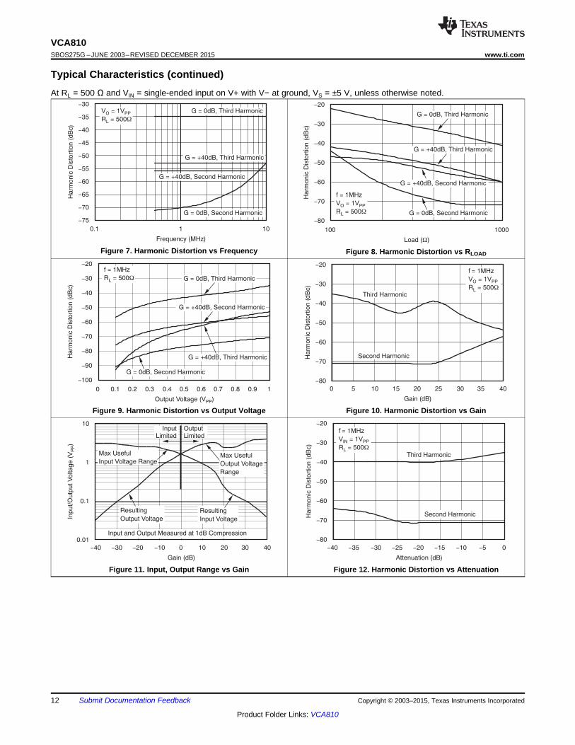
Figure 7. Harmonic Distortion vs Frequency Figure 8. Harmonic Distortion vs RLOAD
Figure 9. Harmonic Distortion vs Output Voltage Figure 10. Harmonic Distortion vs Gain
Figure 11. Input, Output Range vs Gain Figure 12. Harmonic Distortion vs Attenuation
12 Submit Documentation Feedback Copyright © 2003–2015, Texas Instruments Incorporated
Product Folder Links: VCA810

Total Tested = 1462 G = +40dB
Output Offset Voltage (mV)
<50
-
<45
-
<40
-
<35
-
<30
-
<25
-
<20
-
<15
-
<10
- <5
- <0
<5
<10
<15
<20
<25
<30
<35
<40
<45
<50
>50
250
200
150
100
50
0
Count
Control Voltage (V)
0 -0.5 -1 -1.5 -2
Deviation from 40dB/V Gain Slope-
0.4
0.3
0.2
0.1
0
0.1
0.2
0.3
0.4
0.5
-
-
-
-
-
Gain
Err
or
(dB
)
Frequency (Hz)
1M 10M 100M
V = +0.1VC
V = +0.2VC
0
20
40
60
80
100
120
-
-
-
-
-
-
Isola
tion (
dB
)
Gain (dB)
-40 -30 -20 -10 0 10 20 30 40
Maximum Error Band
Typical Devices
50
40
30
20
10
0
10
20
30
40
50-
-
-
-
-
Outp
ut O
ffset E
rror
(mV
)
Control Voltage (V)
0 -0.2 -0.4 -0.6 -0.8 -1.0 -1.2 -1.4 -1.6 -1.8 -2.0
Input-Referred Voltage Noise Density
Output-Referred Voltage Noise Density
R = 20WS
on Each Input
10000
1000
100
10
1
e(n
V/
)n
Hz
e(n
V/
)O
Hz
? ?
Frequency (Hz)
100 1k 10k 100k 1M 10M
Current Noise (1.8pA/ Hz)Ö
Each Input
Differential Input
Voltage Noise (2.4nV/ Hz)Ö
e(n
V/
)n
Hz
i(p
A/
)n
Hz
? ?
10
1
VCA810www.ti.com SBOS275G –JUNE 2003–REVISED DECEMBER 2015
Typical Characteristics (continued)At RL = 500 Ω and VIN = single-ended input on V+ with V− at ground, VS = ±5 V, unless otherwise noted.
Figure 14. Input Voltage and Current NoiseFigure 13. Noise Density vs Control Voltage
Figure 15. Fully Attenuated Isolation vs Frequency Figure 16. Output Offset Voltage Total Error Band vs Gain
Figure 17. Typical Gain Error Plot Figure 18. Output Offset Voltage Distribution
Copyright © 2003–2015, Texas Instruments Incorporated Submit Documentation Feedback 13
Product Folder Links: VCA810

110
100
90
80
70
60
50
40
30
20
10
0
CM
RR
(d
B)
PS
RR
(d
B)
Frequency (MHz)
0.1 1 10 100
PSRR, G = 0dB
CMRR,
G = 40dB±
PSRR,G = +40dB
CMRR,
G = 0dB
0
Gain (dB)
-40 -30 -20 -10 0 10 20 30 40
CMRR
PSRR
Input-Referred110
100
90
80
70
60
50
40
30
20
10
0
CM
RR
(d
B)
PS
RR
(d
B)
Time (100ns/div)
VOUT
10x VIN
2.5
2.0
1.5
1.0
0.5
0
0.5
1.0
1.5
2.0
2.5-
-
-
-
-
Input/O
utp
ut V
oltage (
V)
Time (100ns/div)
VOUT
VIN
200
15
10
5
0
5
10
15
20
25-
-
-
-
-
Inp
ut/
Ou
tpu
t V
olta
ge
(m
V)
Gain (dB)
-40 -30 -20 -10 0 10 20 30 40
V = 1VO PP
R = 500WL
1MHz
5MHz
10MHz
10
9
8
7
6
5
4
Gro
up D
ela
y (
ns)
Frequency (MHz)
1 10 100
V = 1VO PP
R = 500WL
G = 0dB
G = +40dB
10
8
6
4
2
0
Gro
up
De
lay (
ns)
VCA810SBOS275G –JUNE 2003–REVISED DECEMBER 2015 www.ti.com
Typical Characteristics (continued)At RL = 500 Ω and VIN = single-ended input on V+ with V− at ground, VS = ±5 V, unless otherwise noted.
Figure 19. Group Delay vs Gain Figure 20. Group Delay vs Frequency
Figure 21. Overdrive Recovery at Maximum Gain Figure 22. Overdrive Recovery at Maximum Attenuation
Figure 23. Common-Mode Rejection Ratio and Figure 24. Common-Mode Rejection Ratio andPower-Supply Rejection Ratio vs Gain Power-Supply Rejection Ratio vs Frequency
14 Submit Documentation Feedback Copyright © 2003–2015, Texas Instruments Incorporated
Product Folder Links: VCA810

16
14
12
10
8
6
4
2
0
2-
25
20
15
10
5
0
5-
-
-
-
10
15
20
Inp
ut
Bia
s a
nd
Off
se
t C
urr
en
t (
A)
m Ou
tpu
t Offs
et V
olta
ge
(mA
)
Temperature ( C)°
-50 -25 250 50 10075 125
Output Offset Voltage (V )OS
Input Bias Current (I )B
10x Input Offset Current (I )OS
Control Voltage (V)
0 -0.5 -1.0 -1.5 -2.0
Quiescent Current
for V- S
Quiescent Current
for +VS
20
19
18
17
16
15
14
13
12
11
10
Su
pp
ly C
urr
en
t (m
A)
Frequency (Hz)
1k 10k 100k 1M 10M 100M
6
5
4
3
2
1
0
Ga
in (
dB
)
6
5
4
3
2
1
0
Gain
(dB
)
Frequency (Hz)
1k 10k 100k 1M 10M 100M
VCA810www.ti.com SBOS275G –JUNE 2003–REVISED DECEMBER 2015
Typical Characteristics (continued)At RL = 500 Ω and VIN = single-ended input on V+ with V− at ground, VS = ±5 V, unless otherwise noted.
Figure 25. Gain Control +PSRR at Max Gain Figure 26. Gain Control −PSRR at Max Gain
Figure 27. Typical DC Drift vs Temperature Figure 28. Typical Supply Current vs Control Voltage
Copyright © 2003–2015, Texas Instruments Incorporated Submit Documentation Feedback 15
Product Folder Links: VCA810

+5V
-5V
VOUT
VC
0 2V® -
- ®40dB +40dB Gain
VCA810
X1
2
3
V+
V-
1
6
7
5
8
Gain
Adjust
+
G =(V/V) 10-2 (V + 1)C
VCA810SBOS275G –JUNE 2003–REVISED DECEMBER 2015 www.ti.com
8 Detailed Description
8.1 OverviewThe VCA810 is a high gain adjust range, wideband, voltage amplifier with a voltage-controlled gain, as shown inFunctional Block Diagram. The circuit’s basic voltage amplifier responds to the control of an internal gain-controlamplifier. At its input, the voltage amplifier presents the high impedance of a differential stage, permitting flexibleinput impedance matching. To preserve termination options, no internal circuitry connects to the input bases ofthis differential stage. For this reason, the user must provide DC paths for the input base currents from a signalsource, either through a grounded termination resistor or by a direct connection to ground. The differential inputstage also permits rejection of common-mode signals. At its output, the voltage amplifier presents a lowimpedance, simplifying impedance matching. An open-loop design produces wide bandwidth at all gain settings.A ground-referenced differential to single-ended conversion at the output retains the low output offset voltage.
A gain control voltage, VC, controls the amplifier gain magnitude through a high-speed control circuit. Gainpolarity can be either inverting or noninverting, depending upon the amplifier input driven by the input signal. Thegain control circuit presents the high-input impedance of a noninverting operational amplifier connection. Thecontrol voltage pin is referred to ground as shown in Functional Block Diagram. The control voltage VC varies theamplifier gain according to the exponential relationship:
(1)
This translates to the log gain relationship:G(dB) = –40 × (VC + 1)dB (2)
Thus, G(dB) varies linearly over the specified −40 dB to 40 dB range as VC varies from 0 V to −2 V. Optionally,making VC slightly positive (≥ 0.15 V) effectively disables the amplifier, giving greater than 80 dB of signal pathattenuation at low frequencies.
Internally, the gain-control circuit varies the amplifier gain by varying the transconductance, gm, of a bipolartransistor using the transistor bias current. Varying the bias currents of differential stages varies gm to control thevoltage gain of the VCA810. A gm-based gain adjust normally suffers poor thermal stability. The VCA810includes circuitry to minimize this effect.
8.2 Functional Block Diagram
8.3 Feature Description
8.3.1 Input and Output RangeThe VCA810’s 80 dB gain range allows the user to handle an exceptionally wide range of input signal levels. Ifthe input and output voltage range specifications are exceeded, however, signal distortion and amplifier overdrivewill occur. Figure 11 shows the maximum input and output voltage range. This chart plots input and outputvoltages versus gain in dB.
16 Submit Documentation Feedback Copyright © 2003–2015, Texas Instruments Incorporated
Product Folder Links: VCA810

V = V + 10 VOS OSO IOS·
G
20dB( (
VCA810www.ti.com SBOS275G –JUNE 2003–REVISED DECEMBER 2015
Feature Description (continued)The maximum input voltage range is the largest at full attenuation (−40 dB) and decreases as the gain increases.Similarly, the maximum useful output voltage range increases as the input decreases. We can distinguish threeoverloading issues as a result of the operating mode: high attenuation, mid-range gain-attenuation, and highgain.
From –40 dB to –10 dB, gain overdriving the input stage is the only method to overdrive the VCA810. Preventingthis type of overdrive is achieved by limiting the input voltage range.
From –10 dB to 40 dB, overdriving can be prevented by limiting the output voltage range. There are two limitingmechanisms operating in this situation. From –10 dB to 10 dB, an internal stage is the limiting factor; from 10 dBto 40 dB, the output stage is the limiting factor.
Output overdriving occurs when either the maximum output voltage swing or output current is exceeded. TheVCA810 high output current of ±60 mA ensures that virtually all output overdrives will be limited by voltage swingrather than by current limiting. Table 1 summarizes these overdrive conditions.
Table 1. Output Signal CompressionGAIN RANGE LIMITING MECHANISM TO PREVENT, OPERATE DEVICE WITHIN:
−40 dB < G < −10 dB Input Stage Overdrive Input Voltage Range−10 dB < G < 10 dB Internal Stage Overdrive Output Voltage Range
5 dB < G < 40 dB Output Stage Overdrive Output Voltage Range
8.3.2 Overdrive RecoveryAs shown in Figure 11, the onset of overdrive occurs whenever the actual output begins to deviate from the idealexpected output. If possible, the user should operate the VCA810 within the linear regions shown in order tominimize signal distortion and overdrive delay time. However, instances of amplifier overdrive are quite commonin automatic gain control (AGC) circuits, which involve the application of variable gain to input signals of varyinglevels. The VCA810 design incorporates circuitry that allows it to recover from most overdrive conditions in 200ns or less. Overdrive recovery time is defined as the time required for the output to return from overdrive to linearoperation, following the removal of either an input or gain-control overdrive signal. See Typical Characteristics forthe overdrive plots for maximum gain and maximum attenuation.
8.3.3 Output Offset ErrorSeveral elements contribute to the output offset voltage error; among them are the input offset voltage, theoutput offset voltage, the input bias current and the input offset current. To simplify the following analysis, theoutput offset voltage error is dependent only on the output-offset voltage of the VCA810 and the input offsetvoltage. The output offset error can then be expressed as Equation 3:
where• VOS = Output offset error• VOSO = Output offset voltage• GdB = VCA810 gain in dB• VIOS = Input offset voltage (3)
This is shown in Figure 29.
Copyright © 2003–2015, Texas Instruments Incorporated Submit Documentation Feedback 17
Product Folder Links: VCA810

VCA810
1 Fm VCV-
VIN
VOR
V
100kW
R2
10W
V+
R1
10kW
50
40
30
20
10
0
10
20
30
40
50
-
-
-
-
-
Outp
ut O
ffset E
rror
(mV
)
Gain (dB)
-40 -30 -20 -10 0 10 20 30 40
Maximum Error Band
Typical Devices
VCA810SBOS275G –JUNE 2003–REVISED DECEMBER 2015 www.ti.com
Figure 29. Output Offset Error versus Gain
Figure 18 shows the distribution for the output offset voltage at maximum gain.
8.3.4 Offset AdjustmentWhere desired, the offset of the VCA810 can be removed as shown in Figure 30. This circuit simply presents aDC voltage to one of the amplifier inputs to counteract the offset error voltage. For best offset performance, thetrim adjustment should be made with the amplifier set at the maximum gain of the intended application. Theoffset voltage of the VCA810 varies with gain as shown in Figure 29, limiting the complete offset cancellation toone selected gain. Selecting the maximum gain optimizes offset performance for higher gains where highamplification of the offset effects produces the greatest output offset. Two features minimize the offset controlcircuit noise contribution to the amplifier input circuit. First, making the resistance of R2 a low value minimizes thenoise directly introduced by the control circuit. This approach reduces both the thermal noise of the resistor andthe noise produced by the resistor with the amplifier input noise current. A second noise reduction results fromcapacitive bypass of the potentiometer output. This reduction filters out power-supply noise that would otherwisecouple to the amplifier input.
Figure 30. Optional Offset Adjustment
This filtering action diminishes as the wiper position approaches either end of the potentiometer, but practicalconditions prevent such settings. Over its full adjustment range, the offset control circuit produces a ±5-mV inputoffset correction for the values shown. However, the VCA810 only requires one-tenth of this range for offsetcorrection, assuring that the potentiometer wiper will always be near the potentiometer center. With this setting,the resistance seen at the wiper remains high, which stabilizes the filtering function.
18 Submit Documentation Feedback Copyright © 2003–2015, Texas Instruments Incorporated
Product Folder Links: VCA810

RT
VCA810
-5V
EO
VC
IBI
-
+5V
RS
IBN
ENI
ERS
4kTRS
*
*
*
4kTRT
VCA610 VO
RP
CP
VC
f =-3dB
1
2 R CpP P
VCA810www.ti.com SBOS275G –JUNE 2003–REVISED DECEMBER 2015
8.3.5 Gain ControlThe VCA810 gain is controlled by means of a unipolar negative voltage applied between ground and the gaincontrol input, pin 3. If use of the output disable feature is required, a ground-referenced bipolar voltage isneeded. Output disable occurs for 0.15 V ≤ VC ≤ 2 V, and produces greater than 80 dB of attenuation. Thecontrol voltage should be limited to 2 V in disable mode, and –2.5 V in gain mode to prevent saturation of internalcircuitry. The VCA810 gain-control input has a –3-dB bandwidth of 25 MHz and varies with frequency, as shownin Typical Characteristics. This wide bandwidth, although useful for many applications, can allow high-frequencynoise to modulate the gain control input. In practice, this can be easily avoided by filtering the control input, asshown in Figure 31. RP should be no greater than 100 Ω so as not to introduce gain errors by interacting with thegain control input bias current of 6 μA.
Figure 31. Control Line Filtering
8.3.6 Gain Control and Teeple PointWhen the VCA810 control voltage reaches −1.5 V, also referred to as the Teeple point, the signal pathundergoes major changes. From 0 V to the Teeple point, the gain is controlled by one bank of amplifiers: a low-gain VCA. As the Teeple point is passed, the signal path is switched to a higher gain VCA. This gain-stageswitching can be seen most clearly in Figure 13. The output-referred voltage noise density increasesproportionally to the control voltage and reaches a maximum value at the Teeple point. As the gain increasesand the internal stages switch, the output-referred voltage noise density drops suddenly and restarts itsproportional increase with the gain.
8.3.7 Noise PerformanceThe VCA810 offers 2.4-nV/√Hz input-referred voltage noise and 1.8-pA/√Hz input-referred current noise at a gainof 40 dB. The input-referred voltage noise, and the input-referred current noise terms, combine to give low outputnoise under a wide variety of operating conditions. Figure 32 shows the operational amplifier noise analysismodel with all the noise terms included. In this model, all noise terms are taken to be noise voltage or currentdensity terms in either nV/√Hz or pA/√Hz.
Figure 32. VCA810 Noise Analysis Model
Copyright © 2003–2015, Texas Instruments Incorporated Submit Documentation Feedback 19
Product Folder Links: VCA810

External
Pin
+VS
-VS
Internal
Circuitry
ESD Protection diodes internally
connected to all pins.
E = E + (I R ) + 4kT(R + R )N NI BI T S T
2 2+ (I R )BN S
2
E = G E + (I R ) + 4kT(R + R )O NI BI T S T+ (I R )BN S(V/V)·2 2 2
VCA810SBOS275G –JUNE 2003–REVISED DECEMBER 2015 www.ti.com
The total output spot noise voltage can be computed as the square root of the sum of all squared output noisevoltage contributors. Equation 4 shows the general form for the output noise voltage using the terms shown inFigure 32.
(4)
Dividing this expression by the gain will give the equivalent input-referred spot-noise voltage at the noninvertinginput as shown by Equation 5.
(5)
Evaluating these two equations for the VCA810 circuit and component values shown in Figure 34 (maximizinggain) will give a total output spot-noise voltage of 272.3 nV√Hz and a total equivalent input-referred spot-noisevoltage of 2.72 nV√Hz. This total input-referred spot-noise voltage is higher than the 2.4-nV√Hz specification forthe VCA810 alone. This reflects the noise added to the output by the input current noise times the inputresistance RS and RT. Keeping input impedance low is required to maintain low total equivalent input-referredspot-noise voltage.
8.3.8 Input and ESD ProtectionThe VCA810 is built using a very high-speed complementary bipolar process. The internal junction breakdownvoltages are relatively low for these very small geometry devices. These breakdowns are reflected in AbsoluteMaximum Ratings
All pins on the VCA810 are internally protected from ESD by means of a pair of back-to-back, reverse-biaseddiodes to either power supply, as shown in Figure 33. These diodes begin to conduct when the pin voltageexceeds either power supply by about 0.7 V. This situation can occur with loss of the amplifier power supplieswhile a signal source is still present. The diodes can typically withstand a continuous current of 30 mA withoutdestruction. To ensure long-term reliability, however, diode current should be externally limited to 10 mAwhenever possible.
Figure 33. Internal ESD Protection
8.4 Device Functional ModesThe VCA824 functions as a differential input, single-ended output variable gain amplifier. This functional mode isenabled by applying power to the amplifier supply pins and is disabled by turning the power off.
The gain is continuously variable through the analog gain control input. The gain is set by an external, analog,control voltage as shown in the functional block diagram. The signal gain is equal to G = (V/V) 10–2(V + 1) asdetailed in Overview. The gain changes in a linear in dB fashion with over 80 dB of gain range from –2-V to –0-Vcontrol voltage. As with most other differential input amplifiers, inputs can be applied to either one or both of theamplifier inputs. The amplifier gain is controlled through the gain control pin.
In addition to gain control, the gain control pin can also be used to disable the amplifier. This is accomplished byapplying a slightly positive voltage to this pin. This is detailed Feature Description.
20 Submit Documentation Feedback Copyright © 2003–2015, Texas Instruments Incorporated
Product Folder Links: VCA810

VCA810
VC
VI
VO
+5V
6
7
++
2
RC
RT
25W
RL
500W
0.1 Fm
6.8 Fm
35
8
1
-5V
0.1 Fm
6.8 Fm
RS
50W50W
Source
VCA810www.ti.com SBOS275G –JUNE 2003–REVISED DECEMBER 2015
9 Applications and Implementation
NOTEInformation in the following applications sections is not part of the TI componentspecification, and TI does not warrant its accuracy or completeness. TI’s customers areresponsible for determining suitability of components for their purposes. Customers shouldvalidate and test their design implementation to confirm system functionality.
9.1 Application Information
9.1.1 VCA810 OperationFigure 34 shows the circuit configuration used as the basis of the Electrical Characteristics and TypicalCharacteristics. Voltage swings reported in the specifications are taken directly at the input and output pins. Fortest purposes, the input impedance is set to 50 Ω with a resistance to ground. A 25-Ω resistance (RT) is includedon the V− input to get bias current cancellation. Proper supply bypassing is shown in Figure 34, and consists oftwo capacitors on each supply pin: one large electrolytic capacitor (2.2 μF to 6.8 μF), effective at lowerfrequencies, and one small ceramic capacitor (0.1 μF) for high-frequency decoupling.
Figure 34. Variable Gain, Specification and Test Circuit
Notice that both inverting and noninverting inputs are connected to ground with a resistor (RS and RT). Matchingthe DC source impedance looking out of each input will minimize input offset voltage error.
9.1.2 Range-Finding TGC AmplifierThe block diagram in Figure 35 illustrates the fundamental configuration common to pulse-echo range findingsystems. A photodiode preamp provides an initial gain stage to the photodiode.
Copyright © 2003–2015, Texas Instruments Incorporated Submit Documentation Feedback 21
Product Folder Links: VCA810

VCA810
CH
0.1 Fm
V-
VIN
OPA820
VR
V = VOUT PEAK R
VO
R3
1kW HP5082
R1
50kW
2mV to 2V
100kHzRSSIPort
R2
50kW CC
47pF
0.1 VDC
R4
100W
VC
VCA810
VC20W
20W
ADC
and DSP
VC
t0
-2V
Time-Gain Compensated Control Voltage
OPA657
-VB
20kW
CF
VCA810SBOS275G –JUNE 2003–REVISED DECEMBER 2015 www.ti.com
Application Information (continued)
Figure 35. Typical Range-Finding Application
The control voltage VC varies the amplifier gain for a basic signal-processing requirement: compensation fordistance attenuation effects, sometimes called time-gain compensation (TGC). Time-gain compensationincreases the amplifier gain as the signal moves through the air to compensate for signal attenuation. For thispurpose, a ramp signal applied to the VCA810 gain control input linearly increases the dB gain of the VCA810with time.
9.1.3 Wide-Range AGC AmplifierThe voltage-controlled gain feature of the VCA810 makes this amplifier ideal for precision AGC applications withcontrol ranges as large as 60 dB. The AGC circuit of Figure 36 adds an operational amplifier and diode foramplitude detection, a hold capacitor to store the control voltage and resistors R1 through R3 that determineattack and release times. Resistor R4 and capacitor CC phase-compensate the AGC feedback loop. Theoperational amplifier compares the positive peaks of output VO with a DC reference voltage, VR. Whenever a VOpeak exceeds VR, the OPA820 output swings positive, forward-biasing the diode and charging the holdingcapacitor. This charge drives the capacitor voltage in a positive direction, reducing the amplifier gain. R3 and theCH largely determine the attack time of this AGC correction. Between gain corrections, resistor R1 charges thecapacitor in a negative direction, increasing the amplifier gain. R1, R2, and CH determine the release time of thisaction. Resistor R2 forms a voltage divider with R1, limiting the maximum negative voltage developed on CH. Thislimit prevents input overload of the VCA810 gain control circuit.
Figure 37 shows the AGC response for the values shown in Figure 36.
Figure 36. 60-dB Input Range AGC
22 Submit Documentation Feedback Copyright © 2003–2015, Texas Instruments Incorporated
Product Folder Links: VCA810

VCA810
CH
1 Fm
V-
OPA820VR
0.1 VDC
V = VOPEAK R
VO
R3
1kW HP5082
R1
50kW
CW1
4700pF
R4
100W
R2
50kW
RW1
300W
RW2
300W
CW2
4700pF
CC
10pF
f = 1/2 R Cp W1 W1
VC
R = RW1 W2
C = CW1 W2
f =W
1
2 R CpW W
Time (5 s/div)m
V = 10mVIN PP
V = 100mVIN PPV = 1VIN PP
0.15
0.10
0.05
0
0.05
0.10
0.15
0.20-
-
-
-
Outp
ut V
oltage (
50m
V/d
iv)
VCA810www.ti.com SBOS275G –JUNE 2003–REVISED DECEMBER 2015
Application Information (continued)
Figure 37. AGC Output Voltage for 100-kHz Sinewave at 10 mVPP, 100 mVPP, and 1 VPP
9.1.4 Stabilized Wein-Bridge OscillatorAdding Wein-bridge feedback to the above AGC amplifier produces an amplitude-stabilized oscillator. AsFigure 38 shows, this alternative requires the addition of just two resistors (RW1, RW2) and two capacitors(CW1, CW2).
Connecting the feedback network to the amplifier noninverting input introduces positive feedback to induceoscillation. The feedback factor displays a frequency dependence due to the changing impedances of the CWcapacitors. As frequency increases, the decreasing impedance of the CW2 capacitor increases the feedbackfactor. Simultaneously, the decreasing impedance of the CW1 capacitor decreases this factor. Analysis shows
that the maximum factor occurs at Hz, making this the frequency most conducive to oscillation. Atthis frequency, the impedance magnitude of CW equals RW, and inspection of the circuit shows that this conditionproduces a feedback factor of 1/3. Thus, self-sustaining oscillation requires a gain of three through the amplifier.The AGC circuitry establishes this gain level. Following initial circuit turn-on, R1 begins charging CH negative,increasing the amplifier gain from its minimum. When this gain reaches three, oscillation begins at fW; thecontinued charging effect of R1 makes the oscillation amplitude grow. This growth continues until that amplitudereaches a peak value equal to VR. Then, the AGC circuit counteracts the R1 effect, controlling the peak amplitudeat VR by holding the amplifier gain at a level of three. Making VR an AC signal, rather than a DC reference,produces amplitude modulation of the oscillator output.
Figure 38. Amplitude-Stabilized Oscillator
Copyright © 2003–2015, Texas Instruments Incorporated Submit Documentation Feedback 23
Product Folder Links: VCA810

V =OL - 1 +R
R2
1( ( 1 + 0.5 log··
V
VIN
R( (-
V =C
R V
R + R
1 OL
1 2
·
10-2 (V + 1)CV = V = V-OA IN R ·
R1
470W
VCA810
R2
330W
VOL
VR
-10mV
OPA820
VIN
V = GV-OA R
CC
50pF
R3
100W
V = 1 +- 1 + 0.5 Log( V /V )-OL IN R( )VC R
R1
2
G = 10-2 (V + 1)C
VCA810SBOS275G –JUNE 2003–REVISED DECEMBER 2015 www.ti.com
Application Information (continued)9.1.5 Low-Drift Wideband Log AmplifierThe VCA810 can be used to provide a 2.5-MHz (–3 dB) log amp with low offset voltage and low gain drift. Theexponential gain-control characteristic of the VCA810 permits simple generation of a temperature-compensatedlogarithmic response. Enclosing the exponential function in an op-amp feedback path inverts this function,producing the log response. Figure 39 shows the practical implementation of this technique. A DC referencevoltage, VR, sets the VCA810 inverting input voltage. This configuration makes the amplifier output voltage
VOA = −GVR, where .
Figure 39. Temperature-Compensated Log Response
A second input voltage also influences VOA through control of gain G. The feedback operational amplifier forcesVOA to equal the input voltage VIN connected at the operational amplifier inverting input. Any difference betweenthese two signals drops across R3, producing a feedback current that charges CC. The resulting change in VOLadjusts the gain of the VCA810 to change VOA.
At equilibrium:
(6)
The operational amplifier forces this equality by supplying the gain control voltage, .
Combining the last two expressions and solving for VOL yields the circuit’s logarithmic response:
(7)
An examination of this result illustrates several circuit characteristics. First, the argument of the log term, −VIN/VR,reveals an option and a constraint. In Figure 39, VR represents a DC reference voltage. Optionally, making thisvoltage a second signal produces log-ratio operation. Either way, the log term’s argument constrains thepolarities of VR and VIN. These two voltages must be of opposite polarities to ensure a positive argument. Thispolarity combination results when VR connects to the inverting input of the VCA810. Alternately, switching VR tothe amplifier noninverting input removes the minus sign of the log term argument. Then, both voltages must be ofthe same polarity in order to produce a positive argument. In either case, the positive polarity requirement of theargument restricts VIN to a unipolar range. Figure 40 illustrates these constraints.
24 Submit Documentation Feedback Copyright © 2003–2015, Texas Instruments Incorporated
Product Folder Links: VCA810

G = 10-2 (V + 1)C
G
2 R Cp2
f =P
5
4
3
2
1
0
1
2
3
4
5
-
-
-
-
-
Outp
ut V
oltage (
V)
V /VIN R Voltage Ratio
0.001 0.01 0.1 1 10 100
I
II
III
VCA810www.ti.com SBOS275G –JUNE 2003–REVISED DECEMBER 2015
Application Information (continued)
Figure 40. Test Result for LOG Amp for VR = −100 mV
The above VOL expression reflects a circuit gain introduced by the presence of R1 and R2. This feature adds aconvenient scaling control to the circuit. However, a practical matter sets a minimum level for this gain. Thevoltage divider formed by R1 and R2 attenuates the voltage supplied to the VC terminal by the operationalamplifier. This attenuation must be great enough to prevent any possibility of an overload voltage at the VCterminal. Such an overload saturates the VCA810 gain-control circuitry, reducing the amplifier’s gain. For thefeedback connection of Figure 39, this overload condition permits a circuit latch. To prevent this, choose R1 andR2 to ensure that the operational amplifier cannot possibly deliver a more negative input than −2.5 V to the VCterminal.
Figure 40 exhibits three zones of operation described below:
Zone I: VC > 0 V. The VCA810 is operating in full attenuation (−80 dB). The noninverting input of the OPA820will see ∼0 V. VOL is going to be the integration of the input signal.
Zone II: −2 V < VC < 0 V. The VCA810 is in its normal operating mode, creating the log relationship inEquation 7.
Zone III: VC < −2 V. The VCA810 control pin is out of range, and some measure should be taken so that it doesnot exceed –2.5 V. A limiting action could be achieved by using a voltage limiting amplifier.
9.1.6 Voltage-Controlled Low-Pass FilterIn the circuit of Figure 41, the VCA810 serves as the variable-gain element of a voltage-controlled low-pass filter.This section discusses how this implementation expands the circuit voltage swing capability over that normallyachieved with the equivalent multiplier implementation. The circuit response pole responds to control voltage VC,according to the relationship in Equation 8:
where
• (8)
With the components shown, the circuit provides a linear variation of the low-pass cutoff from 300 Hz to 1 MHz.
Copyright © 2003–2015, Texas Instruments Incorporated Submit Documentation Feedback 25
Product Folder Links: VCA810
f =P
G
2 R Cp2
f =P
G
2 R Cp2
OPA820
VCA810
VC
VO
VOA
R2
330W
R1
330W
C
0.047 Fm
VI
G
2 R Cp 2
f =P
V
VO
I
R
R2
1
= -R C
G2 2
1 + s
1·
G = 10-2 (V + 1)C
VCA810SBOS275G –JUNE 2003–REVISED DECEMBER 2015 www.ti.com
Application Information (continued)
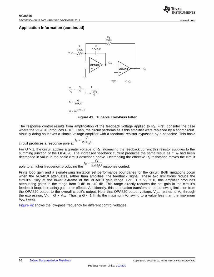
Figure 41. Tunable Low-Pass Filter
The response control results from amplification of the feedback voltage applied to R2. First, consider the casewhere the VCA810 produces G = 1. Then, the circuit performs as if this amplifier were replaced by a short circuit.Visually doing so leaves a simple voltage amplifier with a feedback resistor bypassed by a capacitor. This basic
circuit produces a response pole at .
For G > 1, the circuit applies a greater voltage to R2, increasing the feedback current this resistor supplies to thesumming junction of the OPA820. The increased feedback current produces the same result as if R2 had beendecreased in value in the basic circuit described above. Decreasing the effective R2 resistance moves the circuit
pole to a higher frequency, producing the response control.
Finite loop gain and a signal-swing limitation set performance boundaries for the circuit. Both limitations occurwhen the VCA810 attenuates, rather than amplifies, the feedback signal. These two limitations reduce thecircuit’s utility at the lower extreme of the VCA810 gain range. For −1 ≤ VC ≤ 0, this amplifier producesattenuating gains in the range from 0 dB to −40 dB. This range directly reduces the net gain in the circuit’sfeedback loop, increasing gain error effects. Additionally, this attenuation transfers an output swing limitation fromthe OPA820 output to the overall circuit’s output. Note that OPA820 output voltage, VOA, relates to VO throughthe expression, VO = G × VOA. Thus, a G < 1 limits the maximum VO swing to a value less than the maximumVOA swing.
Figure 42 shows the low-pass frequency for different control voltages.
26 Submit Documentation Feedback Copyright © 2003–2015, Texas Instruments Incorporated
Product Folder Links: VCA810

OPA846
VCA810
VC50W
50W
OPA820
VOA
C
2 Fm
R3
3W
VO
R2
750W
R1
750W
VI
fZ ≈
1
2 (GR + R C)p 1 3with G = 10
-2 (V + 1)C
fZ≈
1
2 R GCp1
fZ≈
1
2 R Cp1
G
2 GR Cp1
fZ≈
Frequency (Hz)
10k 100k 1M 10M
V = 1.4V-C
V = 2V-C
V = 1.6V-C V = 1.8V-C
3
0
3
6
9
12
15-
-
-
-
-
Gain
(dB
)
VCA810www.ti.com SBOS275G –JUNE 2003–REVISED DECEMBER 2015
Application Information (continued)
Figure 42. Voltage-Controlled Low-Pass Filter Frequency Response
9.1.7 Tunable EqualizerA circuit analogous to the above low-pass filter produces a voltage-controlled equalizer response. The gaincontrol provided by the VCA810 of Figure 43 varies this circuit response zero from 1 Hz to 10 kHz, according tothe relationship of Equation 9:
(9)
To visualize the circuit’s operation, consider a circuit condition and an approximation that permit replacing theVCA810 and R3 with short circuits. First, consider the case where the VCA810 produces G = 1. Replacing thisamplifier with a short circuit leaves the operation unchanged. In this shorted state, the circuit is simply a voltageamplifier with an R-C bypass around R1. The resistance of this bypass, R3, serves only to phase-compensate thecircuit, and practical factors make R3 << R1. Neglecting R3 for the moment, the circuit becomes just a voltage
amplifier with a capacitive bypass of R1. This circuit produces a response zero at .
Adding the VCA810 as shown in Figure 43 permits amplification of the signal applied to capacitor C, andproduces voltage control of the frequency fZ. Amplified signal voltage on C increases the signal currentconducted by the capacitor to the operational amplifier feedback network. The result is the same as if C hadbeen increased in value to GC. Replacing C with this effective capacitance value produces the circuit control
expression .
Figure 43. Tunable Equalizer
Copyright © 2003–2015, Texas Instruments Incorporated Submit Documentation Feedback 27
Product Folder Links: VCA810

Q = n · 10- (V + 1)C
=
s +2
+G
R C2 2
s
nRC
s
nRC-
V
V
O
I
fO =10
-(V + 1)C
2 RCp
Frequency (Hz)
1 10 100 1k 10k 100k 1M 10M 100M
G = +40dB
G = +15dB
G = 15dB-
G = 40dB-
AOL
100
90
80
70
60
50
40
30
20
10
0
Gain
(dB
)
VCA810SBOS275G –JUNE 2003–REVISED DECEMBER 2015 www.ti.com
Application Information (continued)Another factor limits the high-frequency performance of the resulting high-pass filter: the finite bandwidth of theoperational amplifier. This limits the frequency duration of the equalizer response. Limitations such as bandwidthand stability are clearly shown in Figure 44.
Figure 44. Amplifier Noise Gain and AOL for Different Gain
Other limitations of this circuit are stability versus VCA810 gain and input signal level for the circuit. Figure 44also illustrates these two factors. As the VCA810 gain increases, the crossover slope between the AOL curve ofthe OPA846 and noise gain will be greater than 20 dB/decade, rendering the circuit unstable. The signal level forhigh gain of the VCA810 will meet two limitations: the output voltage swings of both the VCA810 and theOPA846. The expression VOA = GVI relates these two voltages. Thus, an output voltage limit VOAL constrains theinput voltage to VI ≤ VOAL/G.
With the components shown, BW = 50 kHz. This bandwidth provides an integrator response duration of fourdecades of frequency for fZ = 1 Hz, dropping to one decade for fZ = 10 kHz.
9.1.8 Voltage-Controlled Band-Pass filterThe variable gain of the VCA810 also provides voltage control over the center frequency of a band-pass filter. Asshown in Figure 45, this filter follows from the state-variable configuration with the VCA810 replacing the invertercommon to that configuration. Variation of the VCA810 gain moves the filter’s center frequency through a 100:1range following the relationship of Equation 10:
(10)
As before, variable gain controls a circuit time constant to vary the filter response. The gain of the VCA810amplifies or attenuates the signal driving the lower integrator of the circuit. This amplification alters the effectiveresistance of the integrator time constant, producing the response of Equation 11:
(11)
Evaluation of this response equation reveals a passband gain of AO = –1, a bandwidth of BW = 1/(2πRC), and aselectivity of . Note that variation of control voltage VC alters Q but not bandwidth.
The gain provided by the VCA810 restricts the output swing of the filter. Output signal VO must be constrained toa level that does not drive the VCA810 output, VOA, into its saturation limit. Note that these two outputs havevoltage swings related by VOA = GVO. Thus, a swing limit VOAL imposes a circuit output limit of VOL ≤ VOAL/G.
See Figure 46 for the frequency response for two different gain conditions of the schematic shown in Figure 45.In particular, notice the center frequency shift and the selectivity of Q changing as the gain is increased.
28 Submit Documentation Feedback Copyright © 2003–2015, Texas Instruments Incorporated
Product Folder Links: VCA810

0
5
10
15
20
25
30
35
40
45
50
-
-
-
-
-
-
-
-
-
-
Gain
(dB
)
Frequency (Hz)
100 1k 10k 100k
VCA810
nR
5kW
R
330W
nR
5kW
C
0.047 Fm
VC
R
330W
50W
50W
VOA
C
0.047 Fm
VI
VO
1/2
OPA2822
1/2
OPA2822
=
s +2
+G
R C2 2
s
nRC
s
nRC-
V
VO
I
fO =10
-(V + 1)C
2 RCp
BW =1
2 RCp
(V + 1)C
Q = n-
·10
A = 1-O
VCA810www.ti.com SBOS275G –JUNE 2003–REVISED DECEMBER 2015
Application Information (continued)
Figure 45. Tunable Band-Pass Filter
Figure 46. Tunable Band-Pass Filter Response
Copyright © 2003–2015, Texas Instruments Incorporated Submit Documentation Feedback 29
Product Folder Links: VCA810

Input Voltage (V)
+3.0 +2.5 +2.0 +1.5 +1.0 +0.5 0
1
0.1
0.01
0.001
Outp
ut V
oltage (
V)
R2
330W
VCA810
R1
470W
VR
-10mV
VC
500W 500W
OPA698
VIN
VL
VI
-3.4V
+0.5V V = V- x 10OL R
-2R V
R + R1 IN
1 2
+1( (
VCA810SBOS275G –JUNE 2003–REVISED DECEMBER 2015 www.ti.com
9.2 Typical ApplicationA common use of the log amplifier above involves signal compounding. The inverse function, signal expanding,requires an exponential transfer function. The VCA810 produces this latter response directly, as shown inFigure 47. DC reference VR again sets the amplifier input voltage, and the input signal VIN now drives the gaincontrol point. Resistors R1 and R2 attenuate this drive to prevent overloading the gain control input. Setting theseresistors at the same values as in the preceding log amp produces an exponential amplifier with the inversefunction of the log amplifier.
Testing the circuit given in Figure 47 gives the exponential response shown in Figure 48.
Figure 47. Exponential Amplifier
9.2.1 Design RequirementsTo build a wide dynamic range wide exponential amplifier we need an amplifier with continuous voltage gaincontrol, gain range over 40 dB, low noise, and high maximum gain. The VCA810 has ±40 dB of gain range, so itmeets this criteria. It also has continuous voltage gain control and can support up to 100 V/V of voltage gain.
9.2.2 Detailed Design ProcedureAn exponential amplifier will have a linear response on a logarithmic scale. The linear in dB gain control of theVCA810 is ideal for this application. Note that the input to this circuit is the gain control pin. Using the gaincontrol pin as the input is what gives an exponential gain response. The design involves the use of an OPA698to provide the proper DC bias voltage to the gain control pin on the VCA810. The OPA698 supply voltage waschosen based on the input voltage requirement of the VCA810. The reference voltage (VR) is used to set the DCoutput voltage. The reference voltage cannot be 0 V, but it must be small so that at maximum gain the amplifieroutputs are not saturated. In Figure 47 design the reference voltage is set to –10 mV.
9.2.3 Application Curve
Figure 48. Exponential Amplifier Response
30 Submit Documentation Feedback Copyright © 2003–2015, Texas Instruments Incorporated
Product Folder Links: VCA810

VCA810www.ti.com SBOS275G –JUNE 2003–REVISED DECEMBER 2015
10 Power Supply RecommendationsThe VCA810 is designed for split supply operation with a nominal supply condition of 6 V. A power supply in therange of 8 V to 12 V is acceptable, and balanced supplies (negative and positive voltages equal) arerecommended.
The power supply should be regulated to 10% or better accuracy and capable of sourcing 100 mA of current.The device quiescent current is approximately 20 mA and the load current can be up to 60 mA.
Single supply applications are possible, however, the control voltage is referenced to the ground pin, so a singlesupply application will require a mid supply reference voltage that can be applied to the ground pin. Thisreference voltage should be set to 5% accuracy or better for accurate gain control.
11 Layout
11.1 Layout GuidelinesAchieving optimum performance with a high-frequency amplifier such as the VCA810 requires careful attention toboard layout parasitic and external component types. Recommendations that will optimize performance include:• Minimize parasitic capacitance to any AC ground for all of the signal I/O pins. This includes the ground pin
(pin 2). Parasitic capacitance on the output can cause instability: on both the inverting input and thenoninverting input, it can react with the source impedance to cause unintentional band limiting. To reduceunwanted capacitance, a window around the signal I/O pins should be opened in all of the ground and powerplanes around those pins. Otherwise, ground and power planes should be unbroken elsewhere on the board.Place a small series resistance (> 25 Ω) with the input pin connected to ground to help decouple packageparasitic.
• Minimize the distance (less than 0.25” or 6.35 mm) from the power-supply pins to high-frequency 0.1-μFdecoupling capacitors. At the device pins, the ground and power plane layout should not be in close proximityto the signal I/O pins. Avoid narrow power and ground traces to minimize inductance between the pins andthe decoupling capacitors. The power-supply connections should always be decoupled with these capacitors.Larger (2.2 μF to 6.8 μF) decoupling capacitors, effective at lower frequencies, should also be used on themain supply pins. These capacitors may be placed somewhat farther from the device and may be sharedamong several devices in the same area of the PCB.
• Careful selection and placement of external components will preserve the high-frequency performance of theVCA810. Resistors should be a very low reactance type. Surface-mount resistors work best and allow atighter overall layout. Metal-film and carbon composition, axially-leaded resistors can also provide good high-frequency performance. Again, keep the leads and PCB trace length as short as possible. Never use wire-wound type resistors in a high-frequency application. Since the output pin is the most sensitive to parasiticcapacitance, always position the series output resistor, if any, as close as possible to the output pin. Othernetwork components, such as inverting or noninverting input termination resistors, should also be placedclose to the package.
• Careful selection and placement of external components will preserve the high-frequency performance of theVCA810. Resistors should be a very low reactance type. Surface-mount resistors work best and allow atighter overall layout. Metal-film and carbon composition, axially-leaded resistors can also provide good high-frequency performance. Again, keep the leads and PCB trace length as short as possible. Never use wire-wound type resistors in a high-frequency application. Since the output pin is the most sensitive to parasiticcapacitance, always position the series output resistor, if any, as close as possible to the output pin. Othernetwork components, such as inverting or noninverting input termination resistors, should also be placedclose to the package.
• Socketing a high-speed part like the VCA810 is not recommended. The additional lead length and pin-to-pincapacitance introduced by the socket can create an extremely troublesome parasitic network, which canmake it almost impossible to achieve a smooth, stable frequency response. Best results are obtained bysoldering the VCA810 onto the board.
Copyright © 2003–2015, Texas Instruments Incorporated Submit Documentation Feedback 31
Product Folder Links: VCA810
T = T + P ´ qJ D JAA
VCA810SBOS275G –JUNE 2003–REVISED DECEMBER 2015 www.ti.com
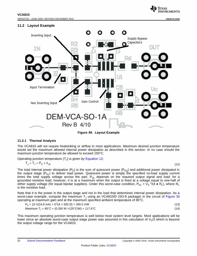
11.2 Layout Example
Figure 49. Layout Example
11.2.1 Thermal AnalysisThe VCA810 will not require heatsinking or airflow in most applications. Maximum desired junction temperaturewould set the maximum allowed internal power dissipation as described in this section. In no case should themaximum junction temperature be allowed to exceed 150°C.
Operating junction temperature (TJ) is given by Equation 12:
(12)
The total internal power dissipation (PD) is the sum of quiescent power (PDQ) and additional power dissipated inthe output stage (PDL) to deliver load power. Quiescent power is simply the specified no-load supply currenttimes the total supply voltage across the part. PDL depends on the required output signal and load; for agrounded resistive load, however, it is at a maximum when the output is fixed at a voltage equal to one-half ofeither supply voltage (for equal bipolar supplies). Under this worst-case condition, PDL = VS.2/(4 RL), where RLis the resistive load.
Note that it is the power in the output stage and not in the load that determines internal power dissipation. As aworst-case example, compute the maximum TJ using an VCA810ID (SO-8 package) in the circuit of Figure 34operating at maximum gain and at the maximum specified ambient temperature of 85°C.
PD = 10 V(24.8 mA) + 52/(4 × 500 Ω) = 260.5 mW (13)Maximum TJ = 85°C + (0.260 W ×125°C/W) = 117.6°C (14)
This maximum operating junction temperature is well below most system level targets. Most applications will belower since an absolute worst-case output stage power was assumed in this calculation of VS/2 which is beyondthe output voltage range for the VCA810.
32 Submit Documentation Feedback Copyright © 2003–2015, Texas Instruments Incorporated
Product Folder Links: VCA810

VCA810www.ti.com SBOS275G –JUNE 2003–REVISED DECEMBER 2015
12 Device and Documentation Support
12.1 Device Support
12.1.1 Development Support
12.1.1.1 Demonstration BoardsA printed circuit board (PCB) is available to assist in the initial evaluation of circuit performance using theVCA810. This evaluation board (EVM) is available free, as an unpopulated PCB delivered with descriptivedocumentation. The summary information for this board is shown in the DEM-VCA-SO-1A user's guide.
12.1.1.2 Macromodels and Applications SupportComputer simulation of circuit performance using SPICE is often useful when analyzing the performance ofanalog circuits and systems. This is particularly true for video and RF amplifier circuits where parasiticcapacitance and inductance can play a major role in circuit performance. A SPICE model for the VCA810 isavailable through the TI web page. The applications group is also available for design assistance. The modelsavailable from TI predict typical small-signal AC performance, transient steps, DC performance, and noise undera wide variety of operating conditions. The models include the noise terms found in the electrical specifications ofthe relevant product data sheet.
12.2 Documentation Support
12.2.1 Related DocumentationUnity-Gain Stable, Low-Noise, Voltage-Feedback Operational Amplifier, SBOS303
12.3 Community ResourcesThe following links connect to TI community resources. Linked contents are provided "AS IS" by the respectivecontributors. They do not constitute TI specifications and do not necessarily reflect TI's views; see TI's Terms ofUse.
TI E2E™ Online Community TI's Engineer-to-Engineer (E2E) Community. Created to foster collaborationamong engineers. At e2e.ti.com, you can ask questions, share knowledge, explore ideas and helpsolve problems with fellow engineers.
Design Support TI's Design Support Quickly find helpful E2E forums along with design support tools andcontact information for technical support.
12.4 TrademarksE2E is a trademark of Texas Instruments.All other trademarks are the property of their respective owners.
12.5 Electrostatic Discharge CautionThese devices have limited built-in ESD protection. The leads should be shorted together or the device placed in conductive foamduring storage or handling to prevent electrostatic damage to the MOS gates.
12.6 GlossarySLYZ022 — TI Glossary.
This glossary lists and explains terms, acronyms, and definitions.
13 Mechanical, Packaging, and Orderable InformationThe following pages include mechanical packaging and orderable information. This information is the mostcurrent data available for the designated devices. This data is subject to change without notice and revision ofthis document. For browser-based versions of this data sheet, refer to the left-hand navigation.
Copyright © 2003–2015, Texas Instruments Incorporated Submit Documentation Feedback 33
Product Folder Links: VCA810

PACKAGE OPTION ADDENDUM
www.ti.com 25-Oct-2016
Addendum-Page 1
PACKAGING INFORMATION
Orderable Device Status(1)
Package Type PackageDrawing
Pins PackageQty
Eco Plan(2)
Lead/Ball Finish(6)
MSL Peak Temp(3)
Op Temp (°C) Device Marking(4/5)
Samples
VCA810AID ACTIVE SOIC D 8 75 Green (RoHS& no Sb/Br)
CU NIPDAU Level-2-260C-1 YEAR -40 to 85 VCA810A
VCA810AIDG4 ACTIVE SOIC D 8 75 Green (RoHS& no Sb/Br)
CU NIPDAU Level-2-260C-1 YEAR -40 to 85 VCA810A
VCA810AIDR ACTIVE SOIC D 8 2500 Green (RoHS& no Sb/Br)
CU NIPDAU Level-2-260C-1 YEAR -40 to 85 VCA810A
VCA810ID ACTIVE SOIC D 8 75 Green (RoHS& no Sb/Br)
CU NIPDAU Level-2-260C-1 YEAR -40 to 85 VCA810
VCA810IDG4 ACTIVE SOIC D 8 75 Green (RoHS& no Sb/Br)
CU NIPDAU Level-2-260C-1 YEAR -40 to 85 VCA810
VCA810IDR ACTIVE SOIC D 8 2500 Green (RoHS& no Sb/Br)
CU NIPDAU Level-2-260C-1 YEAR -40 to 85 VCA810
VCA810IDRG4 ACTIVE SOIC D 8 2500 Green (RoHS& no Sb/Br)
CU NIPDAU Level-2-260C-1 YEAR -40 to 85 VCA810
(1) The marketing status values are defined as follows:ACTIVE: Product device recommended for new designs.LIFEBUY: TI has announced that the device will be discontinued, and a lifetime-buy period is in effect.NRND: Not recommended for new designs. Device is in production to support existing customers, but TI does not recommend using this part in a new design.PREVIEW: Device has been announced but is not in production. Samples may or may not be available.OBSOLETE: TI has discontinued the production of the device.
(2) Eco Plan - The planned eco-friendly classification: Pb-Free (RoHS), Pb-Free (RoHS Exempt), or Green (RoHS & no Sb/Br) - please check http://www.ti.com/productcontent for the latest availabilityinformation and additional product content details.TBD: The Pb-Free/Green conversion plan has not been defined.Pb-Free (RoHS): TI's terms "Lead-Free" or "Pb-Free" mean semiconductor products that are compatible with the current RoHS requirements for all 6 substances, including the requirement thatlead not exceed 0.1% by weight in homogeneous materials. Where designed to be soldered at high temperatures, TI Pb-Free products are suitable for use in specified lead-free processes.Pb-Free (RoHS Exempt): This component has a RoHS exemption for either 1) lead-based flip-chip solder bumps used between the die and package, or 2) lead-based die adhesive used betweenthe die and leadframe. The component is otherwise considered Pb-Free (RoHS compatible) as defined above.Green (RoHS & no Sb/Br): TI defines "Green" to mean Pb-Free (RoHS compatible), and free of Bromine (Br) and Antimony (Sb) based flame retardants (Br or Sb do not exceed 0.1% by weightin homogeneous material)
(3) MSL, Peak Temp. - The Moisture Sensitivity Level rating according to the JEDEC industry standard classifications, and peak solder temperature.

PACKAGE OPTION ADDENDUM
www.ti.com 25-Oct-2016
Addendum-Page 2
(4) There may be additional marking, which relates to the logo, the lot trace code information, or the environmental category on the device.
(5) Multiple Device Markings will be inside parentheses. Only one Device Marking contained in parentheses and separated by a "~" will appear on a device. If a line is indented then it is a continuationof the previous line and the two combined represent the entire Device Marking for that device.
(6) Lead/Ball Finish - Orderable Devices may have multiple material finish options. Finish options are separated by a vertical ruled line. Lead/Ball Finish values may wrap to two lines if the finishvalue exceeds the maximum column width.
Important Information and Disclaimer:The information provided on this page represents TI's knowledge and belief as of the date that it is provided. TI bases its knowledge and belief on informationprovided by third parties, and makes no representation or warranty as to the accuracy of such information. Efforts are underway to better integrate information from third parties. TI has taken andcontinues to take reasonable steps to provide representative and accurate information but may not have conducted destructive testing or chemical analysis on incoming materials and chemicals.TI and TI suppliers consider certain information to be proprietary, and thus CAS numbers and other limited information may not be available for release.
In no event shall TI's liability arising out of such information exceed the total purchase price of the TI part(s) at issue in this document sold by TI to Customer on an annual basis.

TAPE AND REEL INFORMATION
*All dimensions are nominal
Device PackageType
PackageDrawing
Pins SPQ ReelDiameter
(mm)
ReelWidth
W1 (mm)
A0(mm)
B0(mm)
K0(mm)
P1(mm)
W(mm)
Pin1Quadrant
VCA810AIDR SOIC D 8 2500 330.0 12.4 6.4 5.2 2.1 8.0 12.0 Q1
VCA810IDR SOIC D 8 2500 330.0 12.4 6.4 5.2 2.1 8.0 12.0 Q1
PACKAGE MATERIALS INFORMATION
www.ti.com 4-Mar-2014
Pack Materials-Page 1

*All dimensions are nominal
Device Package Type Package Drawing Pins SPQ Length (mm) Width (mm) Height (mm)
VCA810AIDR SOIC D 8 2500 367.0 367.0 35.0
VCA810IDR SOIC D 8 2500 367.0 367.0 35.0
PACKAGE MATERIALS INFORMATION
www.ti.com 4-Mar-2014
Pack Materials-Page 2

IMPORTANT NOTICE
Texas Instruments Incorporated and its subsidiaries (TI) reserve the right to make corrections, enhancements, improvements and otherchanges to its semiconductor products and services per JESD46, latest issue, and to discontinue any product or service per JESD48, latestissue. Buyers should obtain the latest relevant information before placing orders and should verify that such information is current andcomplete. All semiconductor products (also referred to herein as “components”) are sold subject to TI’s terms and conditions of salesupplied at the time of order acknowledgment.TI warrants performance of its components to the specifications applicable at the time of sale, in accordance with the warranty in TI’s termsand conditions of sale of semiconductor products. Testing and other quality control techniques are used to the extent TI deems necessaryto support this warranty. Except where mandated by applicable law, testing of all parameters of each component is not necessarilyperformed.TI assumes no liability for applications assistance or the design of Buyers’ products. Buyers are responsible for their products andapplications using TI components. To minimize the risks associated with Buyers’ products and applications, Buyers should provideadequate design and operating safeguards.TI does not warrant or represent that any license, either express or implied, is granted under any patent right, copyright, mask work right, orother intellectual property right relating to any combination, machine, or process in which TI components or services are used. Informationpublished by TI regarding third-party products or services does not constitute a license to use such products or services or a warranty orendorsement thereof. Use of such information may require a license from a third party under the patents or other intellectual property of thethird party, or a license from TI under the patents or other intellectual property of TI.Reproduction of significant portions of TI information in TI data books or data sheets is permissible only if reproduction is without alterationand is accompanied by all associated warranties, conditions, limitations, and notices. TI is not responsible or liable for such altereddocumentation. Information of third parties may be subject to additional restrictions.Resale of TI components or services with statements different from or beyond the parameters stated by TI for that component or servicevoids all express and any implied warranties for the associated TI component or service and is an unfair and deceptive business practice.TI is not responsible or liable for any such statements.Buyer acknowledges and agrees that it is solely responsible for compliance with all legal, regulatory and safety-related requirementsconcerning its products, and any use of TI components in its applications, notwithstanding any applications-related information or supportthat may be provided by TI. Buyer represents and agrees that it has all the necessary expertise to create and implement safeguards whichanticipate dangerous consequences of failures, monitor failures and their consequences, lessen the likelihood of failures that might causeharm and take appropriate remedial actions. Buyer will fully indemnify TI and its representatives against any damages arising out of the useof any TI components in safety-critical applications.In some cases, TI components may be promoted specifically to facilitate safety-related applications. With such components, TI’s goal is tohelp enable customers to design and create their own end-product solutions that meet applicable functional safety standards andrequirements. Nonetheless, such components are subject to these terms.No TI components are authorized for use in FDA Class III (or similar life-critical medical equipment) unless authorized officers of the partieshave executed a special agreement specifically governing such use.Only those TI components which TI has specifically designated as military grade or “enhanced plastic” are designed and intended for use inmilitary/aerospace applications or environments. Buyer acknowledges and agrees that any military or aerospace use of TI componentswhich have not been so designated is solely at the Buyer's risk, and that Buyer is solely responsible for compliance with all legal andregulatory requirements in connection with such use.TI has specifically designated certain components as meeting ISO/TS16949 requirements, mainly for automotive use. In any case of use ofnon-designated products, TI will not be responsible for any failure to meet ISO/TS16949.
Products ApplicationsAudio www.ti.com/audio Automotive and Transportation www.ti.com/automotiveAmplifiers amplifier.ti.com Communications and Telecom www.ti.com/communicationsData Converters dataconverter.ti.com Computers and Peripherals www.ti.com/computersDLP® Products www.dlp.com Consumer Electronics www.ti.com/consumer-appsDSP dsp.ti.com Energy and Lighting www.ti.com/energyClocks and Timers www.ti.com/clocks Industrial www.ti.com/industrialInterface interface.ti.com Medical www.ti.com/medicalLogic logic.ti.com Security www.ti.com/securityPower Mgmt power.ti.com Space, Avionics and Defense www.ti.com/space-avionics-defenseMicrocontrollers microcontroller.ti.com Video and Imaging www.ti.com/videoRFID www.ti-rfid.comOMAP Applications Processors www.ti.com/omap TI E2E Community e2e.ti.comWireless Connectivity www.ti.com/wirelessconnectivity
Mailing Address: Texas Instruments, Post Office Box 655303, Dallas, Texas 75265Copyright © 2016, Texas Instruments Incorporated