high performance, low cost lateral metal-semiconductor
TRANSCRIPT
High Performance, Low Cost LateralMetal-Semiconductor-Metal
Photodetector for Large AreaIndirect X-Ray Imaging
by
Sina Ghanbarzadeh
A thesis
presented to the University of Waterloo
in fulfillment of the
thesis requirement for the degree of
Master of Applied Science
in
Electrical and Computer Engineering
Waterloo, Ontario, Canada, 2013
c© Sina Ghanbarzadeh 2013

I hereby declare that I am the sole author of this thesis. This is a true copy of the thesis,
including any required final revisions, as accepted by my examiners.
I understand that my thesis may be made electronically available to the public.
ii
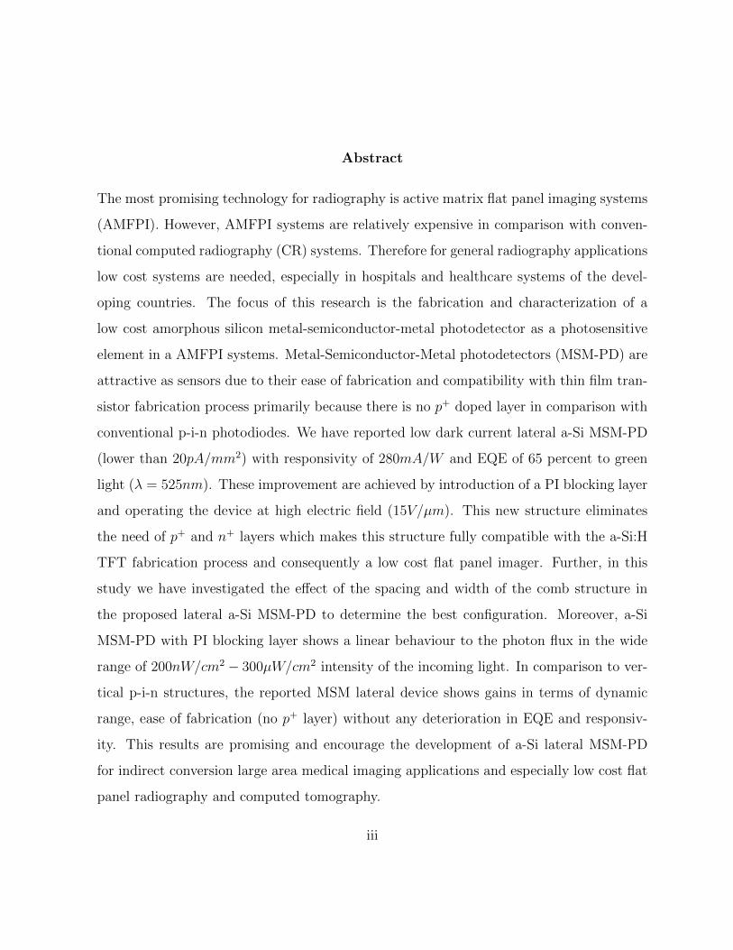
Abstract
The most promising technology for radiography is active matrix flat panel imaging systems
(AMFPI). However, AMFPI systems are relatively expensive in comparison with conven-
tional computed radiography (CR) systems. Therefore for general radiography applications
low cost systems are needed, especially in hospitals and healthcare systems of the devel-
oping countries. The focus of this research is the fabrication and characterization of a
low cost amorphous silicon metal-semiconductor-metal photodetector as a photosensitive
element in a AMFPI systems. Metal-Semiconductor-Metal photodetectors (MSM-PD) are
attractive as sensors due to their ease of fabrication and compatibility with thin film tran-
sistor fabrication process primarily because there is no p+ doped layer in comparison with
conventional p-i-n photodiodes. We have reported low dark current lateral a-Si MSM-PD
(lower than 20pA/mm2) with responsivity of 280mA/W and EQE of 65 percent to green
light (λ = 525nm). These improvement are achieved by introduction of a PI blocking layer
and operating the device at high electric field (15V/µm). This new structure eliminates
the need of p+ and n+ layers which makes this structure fully compatible with the a-Si:H
TFT fabrication process and consequently a low cost flat panel imager. Further, in this
study we have investigated the effect of the spacing and width of the comb structure in
the proposed lateral a-Si MSM-PD to determine the best configuration. Moreover, a-Si
MSM-PD with PI blocking layer shows a linear behaviour to the photon flux in the wide
range of 200nW/cm2 − 300µW/cm2 intensity of the incoming light. In comparison to ver-
tical p-i-n structures, the reported MSM lateral device shows gains in terms of dynamic
range, ease of fabrication (no p+ layer) without any deterioration in EQE and responsiv-
ity. This results are promising and encourage the development of a-Si lateral MSM-PD
for indirect conversion large area medical imaging applications and especially low cost flat
panel radiography and computed tomography.
iii

Acknowledgements
I would like to thank all the people who made this possible.
iv

Dedication
This is dedicated to the one I love.
v

Table of Contents
List of Tables ix
List of Figures x
1 Introduction 1
1.1 Conventional Method for X-Ray Imaging . . . . . . . . . . . . . . . . . . . 2
1.2 Digital Flat Panel Imaging . . . . . . . . . . . . . . . . . . . . . . . . . . . 4
1.2.1 Indirect Conversion . . . . . . . . . . . . . . . . . . . . . . . . . . . 5
1.2.2 Direct Conversion . . . . . . . . . . . . . . . . . . . . . . . . . . . . 6
1.3 Low Cost Direct Radiography Imaging . . . . . . . . . . . . . . . . . . . . 7
1.4 Dark Current Significance . . . . . . . . . . . . . . . . . . . . . . . . . . . 9
1.5 Objective . . . . . . . . . . . . . . . . . . . . . . . . . . . . . . . . . . . . 10
1.6 Thesis Organization . . . . . . . . . . . . . . . . . . . . . . . . . . . . . . . 11
2 Background Theory 13
2.1 Amorphous Silicon Challenges . . . . . . . . . . . . . . . . . . . . . . . . . 13
vi
2.2 History on Metal-Semiconductor-Metal Photodetector . . . . . . . . . . . . 16
2.3 Fundamental of MSM PD . . . . . . . . . . . . . . . . . . . . . . . . . . . 17
2.3.1 Dark Current . . . . . . . . . . . . . . . . . . . . . . . . . . . . . . 17
2.3.2 Photocurrent . . . . . . . . . . . . . . . . . . . . . . . . . . . . . . 23
2.3.3 Capacitance . . . . . . . . . . . . . . . . . . . . . . . . . . . . . . . 24
2.3.4 Dynamic Range . . . . . . . . . . . . . . . . . . . . . . . . . . . . . 26
3 Experimental and Instrumental Methodology 28
3.1 Fabrication Process . . . . . . . . . . . . . . . . . . . . . . . . . . . . . . . 28
3.1.1 Wafer preparing . . . . . . . . . . . . . . . . . . . . . . . . . . . . . 29
3.1.2 a-Si deposition . . . . . . . . . . . . . . . . . . . . . . . . . . . . . 29
3.1.3 Thin Polyimide . . . . . . . . . . . . . . . . . . . . . . . . . . . . . 30
3.1.4 Electrodes . . . . . . . . . . . . . . . . . . . . . . . . . . . . . . . . 32
3.1.5 Device Structure . . . . . . . . . . . . . . . . . . . . . . . . . . . . 33
3.2 Characterization Techniques . . . . . . . . . . . . . . . . . . . . . . . . . . 35
4 Lateral Amorphous Silicon Based MSM Photodetector 36
4.1 Introduction . . . . . . . . . . . . . . . . . . . . . . . . . . . . . . . . . . . 36
4.2 Lateral a-Si MSM (without blocking layer) . . . . . . . . . . . . . . . . . . 37
4.2.1 Dark Current and its instability . . . . . . . . . . . . . . . . . . . . 37
4.2.2 Photoresponse . . . . . . . . . . . . . . . . . . . . . . . . . . . . . . 41
vii
4.3 Introducing the Blocking layer . . . . . . . . . . . . . . . . . . . . . . . . . 43
4.3.1 Dark Current and its stability . . . . . . . . . . . . . . . . . . . . . 43
4.3.2 Photoresponse . . . . . . . . . . . . . . . . . . . . . . . . . . . . . . 46
4.3.3 Responsivity and EQE . . . . . . . . . . . . . . . . . . . . . . . . . 49
4.3.4 Pulse modulation . . . . . . . . . . . . . . . . . . . . . . . . . . . . 52
4.3.5 Linearity to Photon Flux . . . . . . . . . . . . . . . . . . . . . . . . 53
4.3.6 Effect of Electrode Width and Spacing . . . . . . . . . . . . . . . . 56
4.3.7 Wavelength Dependence . . . . . . . . . . . . . . . . . . . . . . . . 62
4.3.8 Temporal Response . . . . . . . . . . . . . . . . . . . . . . . . . . . 64
5 Vertical a-Si MSM Photodetector 66
5.1 Device Structure . . . . . . . . . . . . . . . . . . . . . . . . . . . . . . . . 67
5.2 Dark and Photoresponse . . . . . . . . . . . . . . . . . . . . . . . . . . . . 68
6 Conclusion 71
References 74
viii

List of Tables
1.1 X-ray classification and application base on its energy [1] . . . . . . . . . . 2
2.1 Atomic structure effects on electronic properties in a-Si [2] . . . . . . . . . 16
3.1 PI spin coating process steps . . . . . . . . . . . . . . . . . . . . . . . . . . 32
3.2 Pre-baking process . . . . . . . . . . . . . . . . . . . . . . . . . . . . . . . 32
3.3 Curing process . . . . . . . . . . . . . . . . . . . . . . . . . . . . . . . . . 32
4.1 Physical properties of inorganic phosphors . . . . . . . . . . . . . . . . . . 63
ix

List of Figures
1.1 Schematic of image intensifier. [3] . . . . . . . . . . . . . . . . . . . . . . . . 3
1.2 Schematic of indirect detection technique. [4] . . . . . . . . . . . . . . . . . . 6
1.3 Schematic of direct detection technique. [4] . . . . . . . . . . . . . . . . . . . 7
2.1 Illustration of periodic network of c-Si (a) and random network of a-Si (b). Taken
from [5]. . . . . . . . . . . . . . . . . . . . . . . . . . . . . . . . . . . . . . 14
2.2 Illustration of dansity of state versus energy of c-Si (a) and a-Si (b). Taken from
[5]. . . . . . . . . . . . . . . . . . . . . . . . . . . . . . . . . . . . . . . . . 15
2.3 Electron transport in a-Si layer; F represents the electric field, Et, shows the
Fermi level in a-Si, and w is the depletion width. [6] . . . . . . . . . . . . . . 19
2.4 Transient current cause by dispersive transient. [6, 7] . . . . . . . . . . . . . . 20
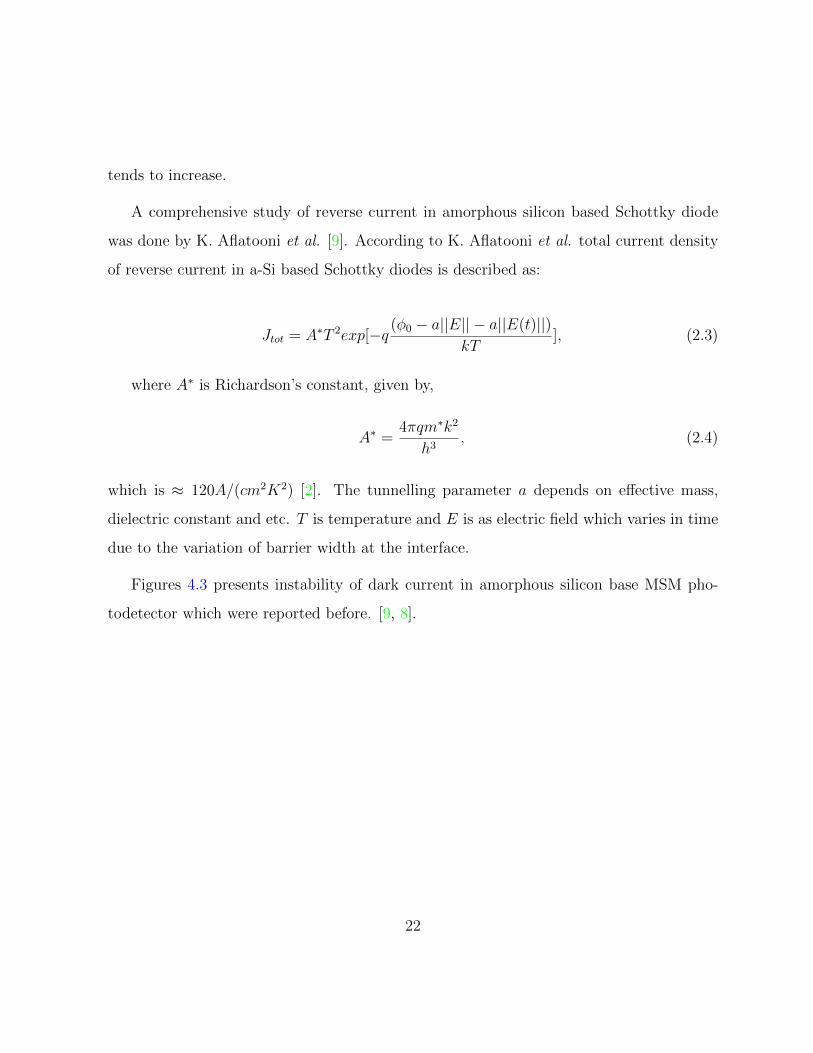
2.5 Dark current instability under constant voltage over time. Reported by (a)
Taghibakhsh et al. [8] (b) Aflatooni et al. [9]. . . . . . . . . . . . . . . . . . . 23
2.6 Lateral Device structure of MSM-PD, (b) Electrode schematic showing comb
structure. . . . . . . . . . . . . . . . . . . . . . . . . . . . . . . . . . . . . 25
2.7 Lateral PPS architecture using a-Si detector for digital imaging . . . . . . . . 27
x
3.1 Cross section of vertical structure. . . . . . . . . . . . . . . . . . . . . . . . 34
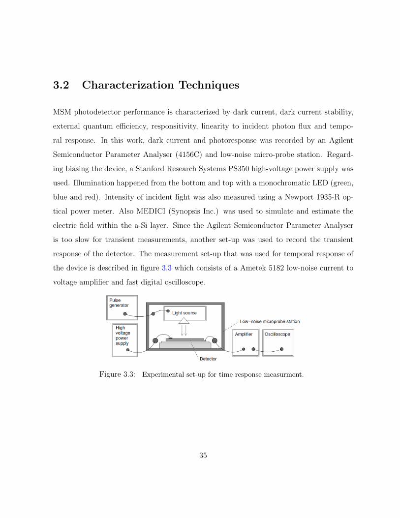
3.2 (a) Lateral a-Si device layout structure (comb structure), (b) Micrograph of
the fabricated detector, and (c) Cross section schematic of a-Si MSM with
blocking layer. . . . . . . . . . . . . . . . . . . . . . . . . . . . . . . . . . . 34
3.3 Experimental set-up for time response measurment. . . . . . . . . . . . . . . 35
4.1 Lateral MSM a-Si:H device structure (left) and lateral MSM a.Si:H with blocking
layer (right). As you can see we have both option of lighting from top and bottom.
Thin PI can be considered transparent for green light. . . . . . . . . . . . . . 37
4.2 Dark current versus voltage for MSM detector without blocking layer. . . . . . 39
4.3 Dark current instability under constant voltage over time. Reported by (a)
Taghibakhsh et al. (b) Aflatooni et al.. . . . . . . . . . . . . . . . . . . . . . 39
4.4 Dark current instability of in house fabricated MSM-PD under constant voltage
of 2.5V . . . . . . . . . . . . . . . . . . . . . . . . . . . . . . . . . . . . . . 40
4.5 Photocurrent density versus voltage of the in-house fabricated a-Si MSM with
width and spacing of 10µ to green light with 73.2µW/cm2 intensity. . . . . . . 42
4.6 Dark and Photoresponse at different voltages for a-Si MSM-PD. Width and spac-
ing of 10µ Incoming light: green light with 73.2µW/cm2 intensity. . . . . . . . 42
4.7 Darkcurrent (before and after illumination) as a function of applied voltage for
a-Si MSM-PD with PI. Width and spacing of 10µ and 15µ respectively. . . . . 44
4.8 Time diagram of darkcurrent measurment. . . . . . . . . . . . . . . . . . . . 44
4.9 Energy level schematic for the a-Si MSM with blocking layer investigated in this
study. . . . . . . . . . . . . . . . . . . . . . . . . . . . . . . . . . . . . . . 45
xi
4.10 Dark current stability of lateral MSM detector with Polyimide Biased at 150V. 46
4.11 Photocurrent density versus voltage of in-house fabricated a-Si MSM with the PI
blocking layer exposed to green light (λ = 525nm) with 9.5µW/cm2 intensity . 47
4.12 Conduction path of the proposed a-Si MSM photodetector with PI blocking layer.
R1 and R3 are the resistance of 100nm PI, R2 is resistance of channel which varies
based on incident light . . . . . . . . . . . . . . . . . . . . . . . . . . . . . . 48
4.13 Photocurrent and dark current as a function of voltage. Dark current was recorded
60sec after illumination. Incident light: Green (λ = 525nm) at intensity of
9.5µW/cm2 . . . . . . . . . . . . . . . . . . . . . . . . . . . . . . . . . . . . 49
4.14 EQE and responsivity of the in-house fabricated a-Si MSM with PI blocking
layer. Incident light: Green (λ = 525nm) at intensity of 10µW/cm2 . . . . 51
4.15 Pulse modulation photoresponse of lateral MSM detector with Polyimide. Inci-
dent light: Green (λ = 525nm) at intensity of 9.5µW/cm2. Pulse period = 50sec
and Width = 20sec . . . . . . . . . . . . . . . . . . . . . . . . . . . . . . . . 52
4.16 Photoresponse versus photon flux at 150V voltage . . . . . . . . . . . . . . . 53
4.17 Normalized responsivity as a function of intensity at 150V and 210V applied
voltage . . . . . . . . . . . . . . . . . . . . . . . . . . . . . . . . . . . . . . 55
4.18 Photocurrent as a function of intensity at 210V bias. This result demonstrates
high detection dynamic rage. Light source: Green (λ = 525nm) . . . . . . . . 55
4.19 (a) Lateral a-Si device layout structure (comb structure), (b) Cross section
schematic of a-Si MSM with PI blocking layer. . . . . . . . . . . . . . . . . 56
4.20 (a) Cross section of simulated device structure (width and spacing of 10µm
(b) Electrical field distribution in amorphous silicon layer in a single device 57
xii
4.21 Photo and darkcurrent of sample 1 (spacing and width of 10µm) and sample 2
(spacing and width of 10µm and 5µm respectively. Light source: Green λ =
525nm at intensity of 9.5µW/cm2) . . . . . . . . . . . . . . . . . . . . . . . 59
4.22 Electrical filed distribution in Polyimide - sample 1 (spacing and width of 10µm) 60
4.23 Top and bottom illumination response at 120V (12V/µm) - Green light at inten-
sity of 10µW/cm2 (spacing and width of 10µm) . . . . . . . . . . . . . . . . . 61
4.24 Responsitivity for three different wavelength. Device: a-Si MSM-PD with thin
PI and width and spacing of 10µm. Intensity: 18µW/cm2. . . . . . . . . . . . 63
4.25 Temporal response of lateral a-Si MSM-PD to pulse light width of 5msec and
period of 10msec. Device is biased at 120V with width and spacing of 10µm .
Light source: Blue - Intensity: 18µW/cm2. . . . . . . . . . . . . . . . . . . . 65
5.1 Cross section of vertical structure. . . . . . . . . . . . . . . . . . . . . . . . 68
5.2 Dark current as a function of voltage in vertical MSM photodetector. . . . . . 69
5.3 Dark and photoresponse of vertical MSM structure. Light source: Green λ =
525nm at intensity of 80µW/cm2. . . . . . . . . . . . . . . . . . . . . . . . . 70
xiii
Chapter 1
Introduction
X-rays have found their place not only in medical imaging, but also in security, industrial
and purely scientific purpose since their discovery in 1895 by German Physicist W. K.
Roentgen. X-ray discovery opened a new phase in medical diagnosis. X-ray allows us
to see things that are invisible to the naked eye and in medicine, it made it possible to
diagnose everything from broken bones to breast cancer. For diagnostic purposes, the
energy range of incident X-rays to the patient are in the range of 20− 120KeV . Typically,
X-ray is categorised by its energy, as shown in table 1.1. Due to the high energy of x-
ray photons, the penetration depth is high and is determined by atomic density of the
attenuating medium. Therefore, density variation, in the medium can be defined by the
x-ray attenuation distribution after exposure.
1
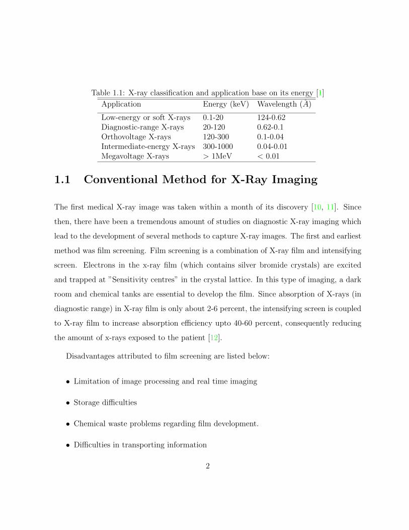
Table 1.1: X-ray classification and application base on its energy [1]
Application Energy (keV) Wavelength (A)
Low-energy or soft X-rays 0.1-20 124-0.62Diagnostic-range X-rays 20-120 0.62-0.1Orthovoltage X-rays 120-300 0.1-0.04Intermediate-energy X-rays 300-1000 0.04-0.01Megavoltage X-rays > 1MeV < 0.01
1.1 Conventional Method for X-Ray Imaging
The first medical X-ray image was taken within a month of its discovery [10, 11]. Since
then, there have been a tremendous amount of studies on diagnostic X-ray imaging which
lead to the development of several methods to capture X-ray images. The first and earliest
method was film screening. Film screening is a combination of X-ray film and intensifying
screen. Electrons in the x-ray film (which contains silver bromide crystals) are excited
and trapped at ”Sensitivity centres” in the crystal lattice. In this type of imaging, a dark
room and chemical tanks are essential to develop the film. Since absorption of X-rays (in
diagnostic range) in X-ray film is only about 2-6 percent, the intensifying screen is coupled
to X-ray film to increase absorption efficiency upto 40-60 percent, consequently reducing
the amount of x-rays exposed to the patient [12].
Disadvantages attributed to film screening are listed below:
• Limitation of image processing and real time imaging
• Storage difficulties
• Chemical waste problems regarding film development.
• Difficulties in transporting information
2
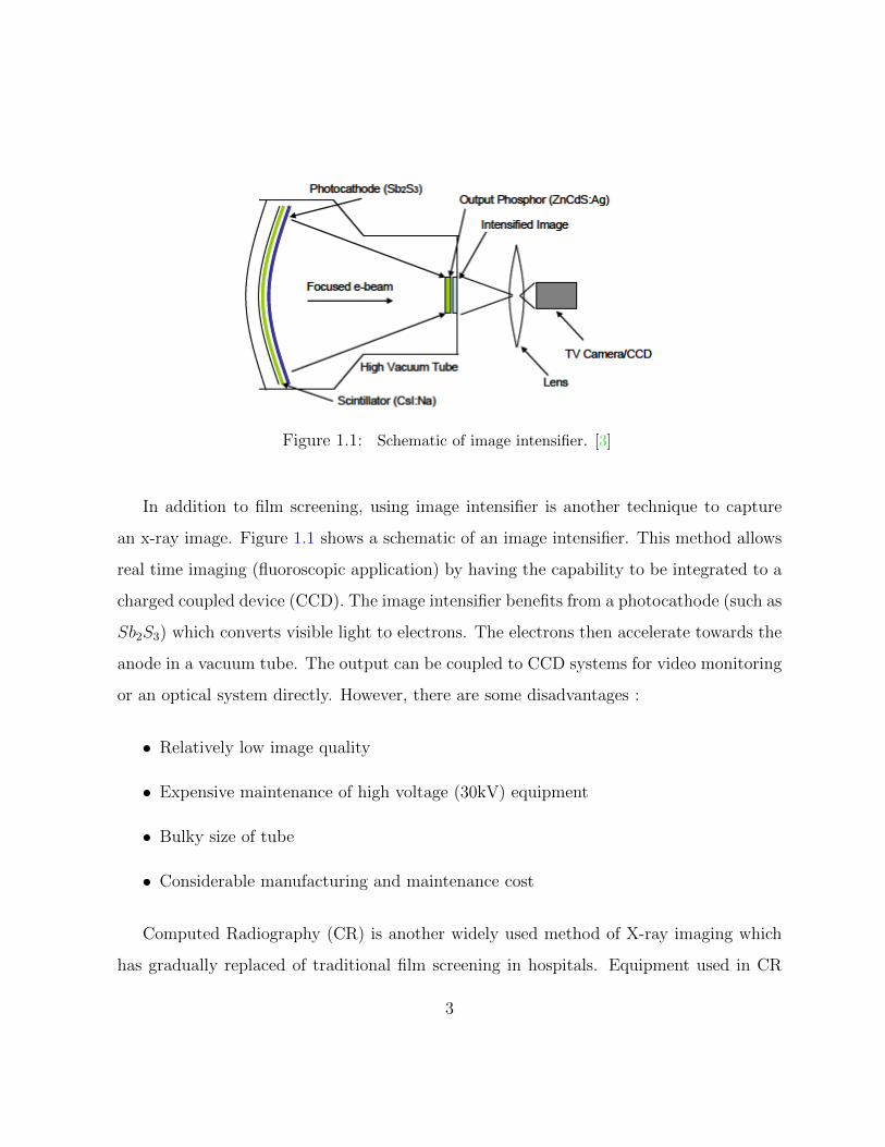
Figure 1.1: Schematic of image intensifier. [3]
In addition to film screening, using image intensifier is another technique to capture
an x-ray image. Figure 1.1 shows a schematic of an image intensifier. This method allows
real time imaging (fluoroscopic application) by having the capability to be integrated to a
charged coupled device (CCD). The image intensifier benefits from a photocathode (such as
Sb2S3) which converts visible light to electrons. The electrons then accelerate towards the
anode in a vacuum tube. The output can be coupled to CCD systems for video monitoring
or an optical system directly. However, there are some disadvantages :
• Relatively low image quality
• Expensive maintenance of high voltage (30kV) equipment
• Bulky size of tube
• Considerable manufacturing and maintenance cost
Computed Radiography (CR) is another widely used method of X-ray imaging which
has gradually replaced of traditional film screening in hospitals. Equipment used in CR
3
imaging is very similar to film screening expect that in place of the film to create image, an
imaging plate (IP) made of photostimulatable phosphor is used. This method can be used
to creat a digital image. The IP stores energy and is scanned by red laser light to develop
the image. Therefore computed radiography provides feasibility of image processing to
enhance quality of the image.
1.2 Digital Flat Panel Imaging
Digital flat panel X-ray image detectors are the most promising technique for radiography.
Ideally, an x-ray imaging system should provide instantaneous and real-time imaging in a
digital format with the least amount of exposure as well as reasonable manufacturing and
maintenance cost. Conventional X-ray imaging systems, as mentioned, take advantage of
photostimulatable phosphor plates (i.e. CR) which prevents any instantaneous and real-
time imaging and in order to digitize the image information, scanning by laser system is
necessary. Therefore, like traditional film screening, this technique is time consuming and
the quality of the image is poor in comparison.
Digital flat panel imaging system are compromised two main components:
1. X-ray detector: Convert X-ray to electrical charge
2. Readout circuit: Store and transfer electrical charge to off-panel circuitry.
Optical imaging systems have a major difference in compared to X-ray imaging. Optical
imaging benefits from lenses which project large area field of view on to a device the size
of fingernail. On the other hand, x-rays, cannot be focused, so in order to capture x-ray an
image of the chest or any other parts of body, an imager with that size is required. Thus,
4
taking advantage of crystalline silicon technology is limited and tiling would be required
to manufacture a large area detector, for example 20cm by 20cm (chest radiography).
Conversely, active matrix flat panel imagers (AMFPI) offer great advantage in term of size
of the detector. AMFPI uses thin film transistors (TFTs) which are compatible with large
are fabrication.
Currently there are two techniques to detect x-rays in flat panel imagers. One is utilizing
a photoconductor to convert incident x-ray photons to electrical charge so called as direct
conversion. The other is indirect conversion which benefits from a phosphor layer (also
known as scintillator) to convert X-ray to visible light and a photodetector which converts
visible light to electrical charge.
1.2.1 Indirect Conversion
Figure 1.2 demonstrates mechanism of indirect detection. Here a phosphor layer (typically
Gd2S : Tb or CsI : T l) is placed in intimate contact with the active matrix array. The
phosphor layer converts X-ray photons to light with a specific conversion gain at a certain
wavelength (conversion gain is defined as the number of emitted photons per incident X-
ray photon). The intensity of light emitted from a particular location of the phosphor
is proportional to the intensity of the incident x-ray photons. In order to convert light
to electrical charge, each pixel in the active matrix has a photosensitive element (which
can be either Schottky M-I-S/M-S-M diode or p-i-n photodiode). The amount of charge
determines intensity of light emitted from the phosphor in the region near the pixel. In this
type of detection the total conversion gain is a product of scintillator conversion efficiency
and the effective quantum efficiency [13]. Hence in order to achieve maximum efficiency,
the peak of the emission spectrum of the scintillator should match the absorption spectrum
5
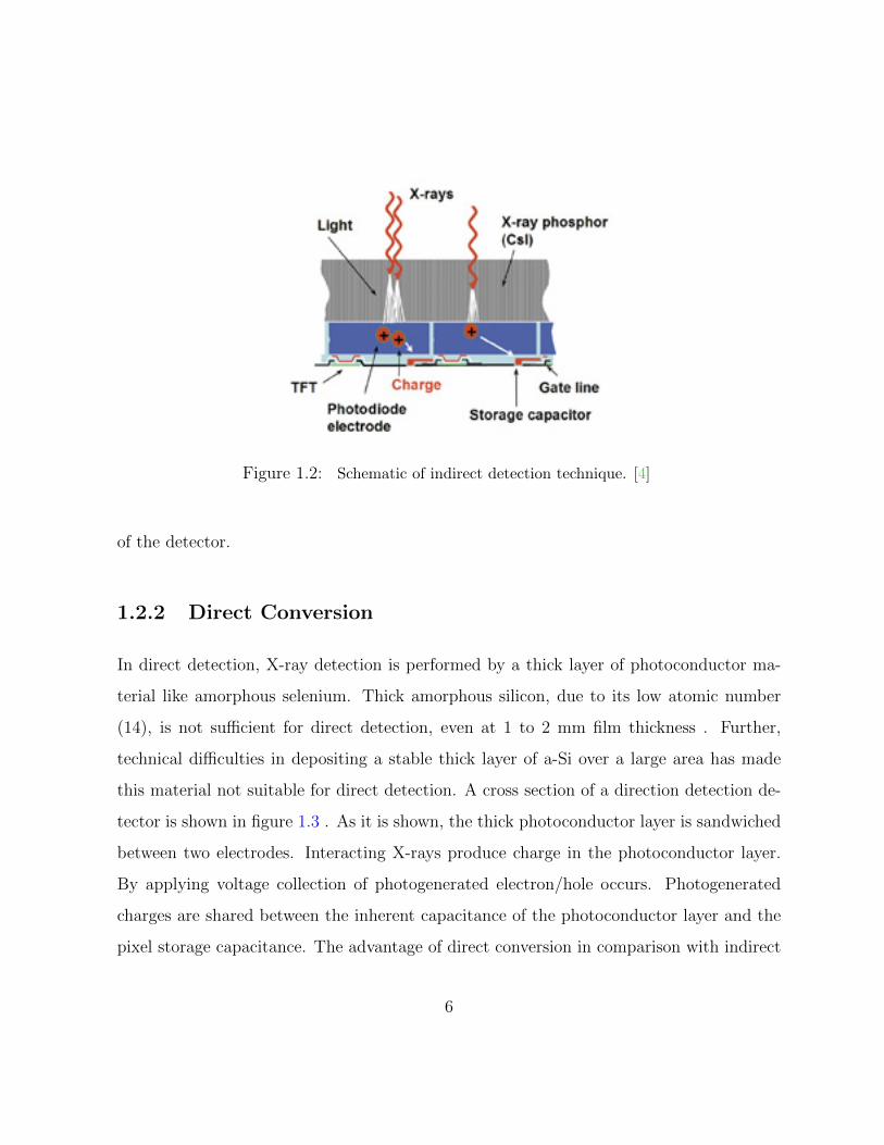
Figure 1.2: Schematic of indirect detection technique. [4]
of the detector.
1.2.2 Direct Conversion
In direct detection, X-ray detection is performed by a thick layer of photoconductor ma-
terial like amorphous selenium. Thick amorphous silicon, due to its low atomic number
(14), is not sufficient for direct detection, even at 1 to 2 mm film thickness . Further,
technical difficulties in depositing a stable thick layer of a-Si over a large area has made
this material not suitable for direct detection. A cross section of a direction detection de-
tector is shown in figure 1.3 . As it is shown, the thick photoconductor layer is sandwiched
between two electrodes. Interacting X-rays produce charge in the photoconductor layer.
By applying voltage collection of photogenerated electron/hole occurs. Photogenerated
charges are shared between the inherent capacitance of the photoconductor layer and the
pixel storage capacitance. The advantage of direct conversion in comparison with indirect
6
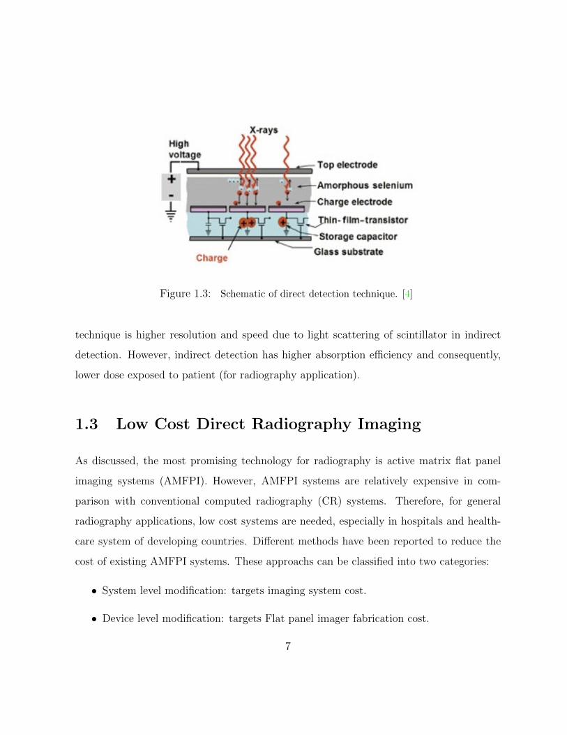
Figure 1.3: Schematic of direct detection technique. [4]
technique is higher resolution and speed due to light scattering of scintillator in indirect
detection. However, indirect detection has higher absorption efficiency and consequently,
lower dose exposed to patient (for radiography application).
1.3 Low Cost Direct Radiography Imaging
As discussed, the most promising technology for radiography is active matrix flat panel
imaging systems (AMFPI). However, AMFPI systems are relatively expensive in com-
parison with conventional computed radiography (CR) systems. Therefore, for general
radiography applications, low cost systems are needed, especially in hospitals and health-
care system of developing countries. Different methods have been reported to reduce the
cost of existing AMFPI systems. These approachs can be classified into two categories:
• System level modification: targets imaging system cost.
• Device level modification: targets Flat panel imager fabrication cost.
7
In system level modification, we can consider scanned projection x-ray which was re-
ported by M. J. Yaffe et al. [14]. In this technique instead of a two dimensional detector,
a one-dimensional image receptor used. The second dimensional is obtained by scanning
the x-ray beam and detector across patient. This technique demonstrated an improvement
in scattered radiation rejection [14]. Further the cost of the detector is decreased due to
the single dimension needed. However, this method requires quite complex and accurate
mechanical systems to synchronize scanning of the x-ray tube and the detector. Another
method that may reduce cost of the digital radiography system is optically demagnified
x-ray screen/camera system. Theoretically, this approach requires a low cost screen and a
CCD or even CMOS digital camera. However, coupling x-ray film to a cheap CCD camera
without a secondary quantum sink (such as a lens) would result in poor DQE and no
significant demagnification [15]. Also introducing a lens raises the cost of the detector and
in the best case, quality and cost of the detector would be the same as indirect detection
with AMFPI system (which due to the identical size of the screen and flat panel, such that
100 percent optical coupling occurs).
Another approach to lower cost is reducing the cost of flat panel imager itself. Digital
flat panel technology initially targeted indirect detection. Active matrix technology that is
used in flat panel imagers is the same as standard a-Si:H TFT manufacturing technology
used to make displays. One part of AMFPIs that increases the cost is the photosensitive
element. Currently most AMFPIs take advantage of p-i-n photodiodes primarily due to
their low leakage current, high quantum efficiency. However due to existence of doped
p+ layer, fabrication of photosensitive elements cannot perform with the same process of
a-Si:H TFT and it requires separate process which increases final cost of AMFPI. On the
other hand, eliminating p+ layer would increase dark current which is not favourable for
detector performance.
8
1.4 Dark Current Significance
To have an efficient collection process within the photoconductor (direct detection) or
photosensitive element of AMFPIs (indirect detection), application of an electrical field is
required. By applying an external voltage, photogenerated electrons and holes will flow
towards anode and cathode respectively. However, even in absence of x-rays, current will
flow through the photodetector, i.e. so-called dark current. Dark current of the photode-
tector determines the lowest amount of x-ray that is detectable by a single pixel of the
detector. Thus, having high dark current corresponds to higher exposure of x-rays to the
patient in order to be detectable. In addition to shrinking dynamic range of the detector,
dark current introduces noise into readout circuity of the AMFPI which increases with the
amplitude of the dark current. Typically dark current of photoconductor should not ex-
ceed 20pA/mm2 [13] especially in integration mode of imaging like computed tomography
and general radiography. In fluoroscopy, (real-time imaging) higher dark current is less
problematic in comparison with integration mode imaging. In AMFPIs, the photosensitive
elements are typically p-i-n photodiodes. Dark current in amorphous silicon stems from
two mechanisms. Thermal generation of amorphous silicon and injection of carriers from
anode and cathode. Thermal generation of a-Si for a 1mm by 1mm device with thickness
of 500nm is approximately 2-3 pA (it will calculate in next chapter). However by applying
voltage, the dominant source of dark current is injection of carriers from electrodes. p-i-n
photodiodes exhibit great performance because of their high quantum efficiency and low
dark current (p and n layers block carrier injection). However, as mentioned earlier, the
fabrication of p-i-n photodiodes (due to doped p+ layer) should be performed separately
from a-Si:H TFTs, making the detector relatively expensive.
9
1.5 Objective
The focus of this research is primarily related to the investigation of possibilities to cre-
ate a low cost indirect conversion digital x-ray imager utilizing amorphous silicon metal-
semiconductor-metal (MSM) photodetector as a photosensitive element in a flat panel
imager. The criteria considered for the MSM photodetector is performance quality and
potential to be manufacturable as a low cost digital radiography system to permit its use
for general application, especially in hospitals and healthcare systems in developing coun-
tries. In order to lower cost of the x-ray imager, in this work we a propose new structure
of a-Si MSM-PD as a replacement for p-i-n photodiode which is commercially used as
the photosensitive element in flat panel imagers. The main challenge in this research was
finding an approach to minimize dark current without any significant deterioration in its
performance through systematic studies on photoresponse of the detector. In this study,
in order to achieve the optimum MSM structure having low dark current and compara-
ble quantum efficiency to a p-i-n photodiode, over 100 devices have been produced. The
experiments that were carried out to characterize the proposed structure are addressed
below:
• Investigation of dark current mechanisms and its stability in proposed a-Si MSM-PD
• Investigation of responsivity and quantum efficiency at different electrical fields.
• Study the effect of fill factor and electrode spacing/width on dark and photocurrent.
• Investigation of detector behaviour under incident power at high and low electrical
fields.
• Investigation of temporal response
10
• Fabrication and study of vertical MSM structure and address challenges
Previously reported a-Si MSM photodetectors exhibit high dark current, dark current
instability, low dynamic range and limited EQE to fill factor [16, 8]. Based on results of
experiments, we have been able to propose a lateral MSM structure as an alternative to
the p-i-n photodiode. These improvement are achieved by introduction of a thin polymer
(polyimide) layer as a blocking layer and operating device at high electric field (15V/µm).
This new structure eliminates the need of p+ and n+ layers which makes this structure
fully compatible with the a-Si:H TFT fabrication process and consequently a low cost flat
panel imager. These results are promising and encourage the development of a-Si lateral
MSM devices for indirect conversion large area medical imaging applications, especially for
low-cost flat panel radiography and computed tomography.
1.6 Thesis Organization
This chapter has described introductory information on conventional methods for medical
imaging, digital flat panel imagers and the importance of low cost x-ray imaging systems.
Further, we discussed that in order to bring down the cost of flat panel imagers, a re-
placement for the p-i-n photodiode as a photosensitive element in flat panel imagers is
needed. The next chapter covers brief background information on amorphous silicon and
history of the MSM photodetector, followed by fundamentals of a-Si MSM photodetectors
including dark current, photocurrent and dynamic range. In chapter 3, the fabrication
process of both lateral and vertical structure are briefly described and continues with a
brief description of characterization techniques that were used in this work.
Chapter 4 starts with demonstrating improvement of dark current and dark current
11
stability of the proposed lateral MSM structure without any deterioration in its respon-
sivity. In following, high external quantum efficiency (about 66 percent) is demonstrated
and it is discussed that by introducing an anti-reflective layer, EQE can rise up to 80-85
percent. The chapter continues with a study of fill factor and the effect of electrode spac-
ing and width to suggest the best configuration. Further, this chapter covers linearity and
non-linearity behaviour of the detector to incident photon flux at high and low electric
field. Finally, the detector’s temporal response is studied and we demonstrate fall and
rise time of 1 ms for 10µm spacing and width. In chapter 5, the performance (dark and
photo response) of the vertical MSM structure is presented and remaining challenges are
addressed to improve EQE. Lastly, Chapter 6 concludes this work and summarizes the
contributions of this thesis to the field of amorphous silicon technology.
12
Chapter 2
Background Theory
2.1 Amorphous Silicon Challenges
Amorphous silicon in comparison to crystalline silicon offers some advantages and disad-
vantages. On the good side, a-Si provides high absorption efficiency within the thin layer
(300 - 500 nm), low cost process and large area fabrication which are essential for digital flat
panel imagers. On the other hand, due to lack of long range order in amorphous silicon, the
density of state concept needs to be revised. However, amorphous silicon retains its short
range order because covalent bonds of silicon in a-Si are relatively similar to silicon bonds
in crystalline silicon in terms of bond angles, length and number of neighbouring atoms [2].
Since short range order is preserved in a-Si and the energy bond diagram strongly depends
on local band configuration [17], with some modifications, DOS of crystalline silicon is
applicable to amorphous silicon.
Figure 2.1 illustrates the difference between an atomic network of crystalline silicon
and amorphous silicon. Loss of long range order in amorphous silicon results in deviation
13
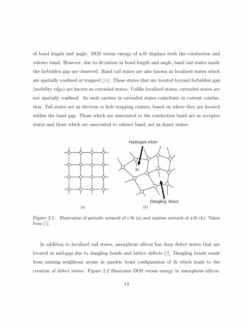
of bond length and angle. DOS versus energy of a-Si displays both the conduction and
valence band. However, due to deviation in bond length and angle, band tail states inside
the forbidden gap are observed. Band tail states are also known as localized states which
are spatially confined or trapped [18]. Those states that are located beyond forbidden gap
(mobility edge) are known as extended states. Unlike localized states, extended states are
not spatially confined. As such carriers in extended states contribute in current conduc-
tion. Tail states act as electron or hole trapping centers, based on where they are located
within the band gap. Those which are associated to the conduction band act as acceptor
states and those which are associated to valence band, act as donor states.
Figure 2.1: Illustration of periodic network of c-Si (a) and random network of a-Si (b). Takenfrom [5].
In addition to localized tail states, amorphous silicon has deep defect states that are
located at mid-gap due to dangling bonds and lattice defects [2]. Dangling bonds result
from missing neighbour atoms in quadric bond configuration of Si which leads to the
creation of defect states. Figure 2.2 illustrates DOS versus energy in amorphous silicon.
14
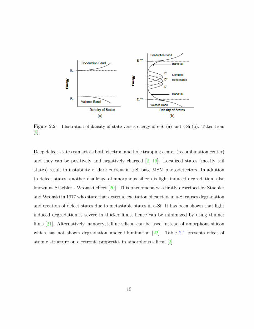
Figure 2.2: Illustration of dansity of state versus energy of c-Si (a) and a-Si (b). Taken from[5].
Deep defect states can act as both electron and hole trapping center (recombination center)
and they can be positively and negatively charged [2, 19]. Localized states (mostly tail
states) result in instability of dark current in a-Si base MSM photodetectors. In addition
to defect states, another challenge of amorphous silicon is light induced degradation, also
known as Staebler - Wronski effect [20]. This phenomena was firstly described by Staebler
and Wronski in 1977 who state that external excitation of carriers in a-Si causes degradation
and creation of defect states due to metastable states in a-Si. It has been shown that light
induced degradation is severe in thicker films, hence can be minimized by using thinner
films [21]. Alternatively, nanocrystalline silicon can be used instead of amorphous silicon
which has not shown degradation under illumination [22]. Table 2.1 presents effect of
atomic structure on electronic properties in amorphous silicon [2].
15
Table 2.1: Atomic structure effects on electronic properties in a-Si [2]
Atomic Structure Electronic Properties
Bonding Disorder Band tails, localization, scatteringStructural Defects Electronic states within the bandgapAlternative bonding configurations Metastable states
2.2 History on Metal-Semiconductor-Metal Photode-
tector
Metal-Semiconductor-Metal photodetector (MSM-PD) are attractive as sensors due to
their ease of fabrication and compatibility with thin film transistor fabrication process
and/or field-effect-transistors (FETs) in optoelectronic integrated circuits (OEICSs) [23]
primarily because there is no p+ doped layer in comparison with conventional p-i-n pho-
todiodes. Moreover, these type of detector would dramatically lower cost and MSM-PDs
have demonstrated high operation speed primarily due to low capacitance and consequently
lower RC constant time.
MSM structure was first studied at Bell Telephone Laboratories by S. M. Sze et al. in
1971 [24]. In 1979, the first MSM photodetector was proposed for high speed optoelectronic
circuits, followed by other structures from C. W. Slayman, L. Figueroa and C. J. Wei et al.
[25, 26, 27]. Between 1988 to 1999, in order to reduce dark current in MSM-PDs, the idea
of introducing different passivation layers had obtained much interest among researchers.
Sulfured passivation layer for Schottky contacts [28, 29, 30], ultra-thin Au islands [31],
introducing SiO2 layer for InGaAs base MSM-PD [32, 33] and also Polyimide passivation
layer [34] have all been studied. Since then, there has been much progress to improve
MSM-PD performance in terms of sensitivity, efficiency and speed. The speed of detectors
is determined by transient time of photogenerated charge carriers and RC constant time
16
(charging time) of the external circuit. Typically, transient time of coplanar MSM-PD
is less than conventional p-i-n structure due to long travelling distance for carriers in
MSM structure in comparison with p-i-n photodiodes. One of the common ways to reduce
transient time is shrinking the spacing between electrodes. However, this would increase
capacitance of MSM-PD. Therefore there is always a trade-off between these two factors. In
literature different MSM structures have been proposed to compromise between transient
time andRC time constant [35, 36]. Moreover, there has been some effort to solve the trade-
off problem by introducing trench-electrodes Si base MSM [37, 38, 39, 40, 41]. However to
fabricate trench electrode reactive ion etching (RIE) is required which makes fabrication
complex and expensive due to two stage photolithography. Basically, amorphous silicon
MSM structure are favourable for large area medical imaging from an integration point
of view and large area fabrication compatibility. Recently a-Si base MSM-PD for indirect
large area medical imaging application has been reported [16, 8]. However the earlier
devices exhibited high dark current which is problematic for integration mode imaging. In
the other words, they were limited in term of dynamic range. Furthermore in the year 2013
Molybdenum disulfide and amorphous silicon heterojunction MSM photodetector has been
proposed to improve transient response for fast imaging application such as fluoroscopy
imaging [42]
2.3 Fundamental of MSM PD
2.3.1 Dark Current
Charge transport in amorphous silicon is primarily due to two mechanisms, Band-like
transport (mobile and extended states) and hopping transport (localized states). Both
17
mechanisms contribute in reverse current of the Schottky diode. Dark current in Metal-
Semiconductor-Metal Schottky diodes stems from four sources: [2, 43, 44, 45, 46]
1. Thermal generation
2. Trapped charges
3. Thermionic emission
4. Tunnelling through junction barrier
MSM photodetectors consist of two back-to-back Schottky diodes. In symmetric MSM
photodetectors, metal/semiconductor barrier for both contacts are the same. By applying
voltage, one of the diodes will be in reverse mode and the other in forward bias, so most
of the voltage would be across the diode which is in reverse mode. Hence, dark current of
the MSM structure is determined by reverse current of the Schottky metal/semiconductor
contact. The dominant component of dark current is determined by the magnitude of
applied voltage [47, 9]. At low voltage (low electrical fields at interface) prevailing sources
of current are thermal generation and trapped charges in deep defect states. On the other
hand, dominant components of dark current at higher electrical field are tunnelling and
thermionic emission (also called thermionic field emission).
In the low voltage case (E < 2 × 10⁵V/cm2), charge carriers at the conduction band
and extended states would sweep away to the output terminal quickly. At this time, the
balance between mid-gap states and extended states would be removed. Those mid-gap
states which are located below Fermi level are occupied by electrons. After a short time of
applying bias and disturbing the equilibrium, electrons in mid-gap states will gain enough
energy to reach the conduction band and contribute to dark current. These released charges
from mid-gap states would also experience scattering phenomena during travel towards the
18
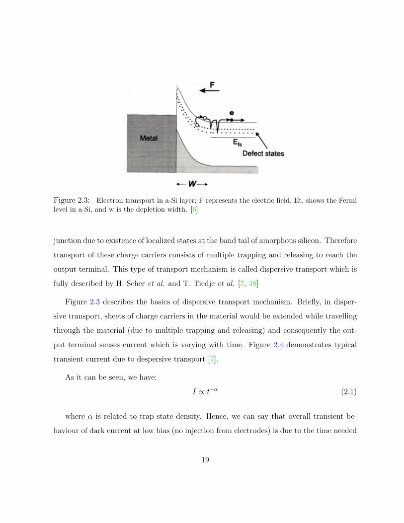
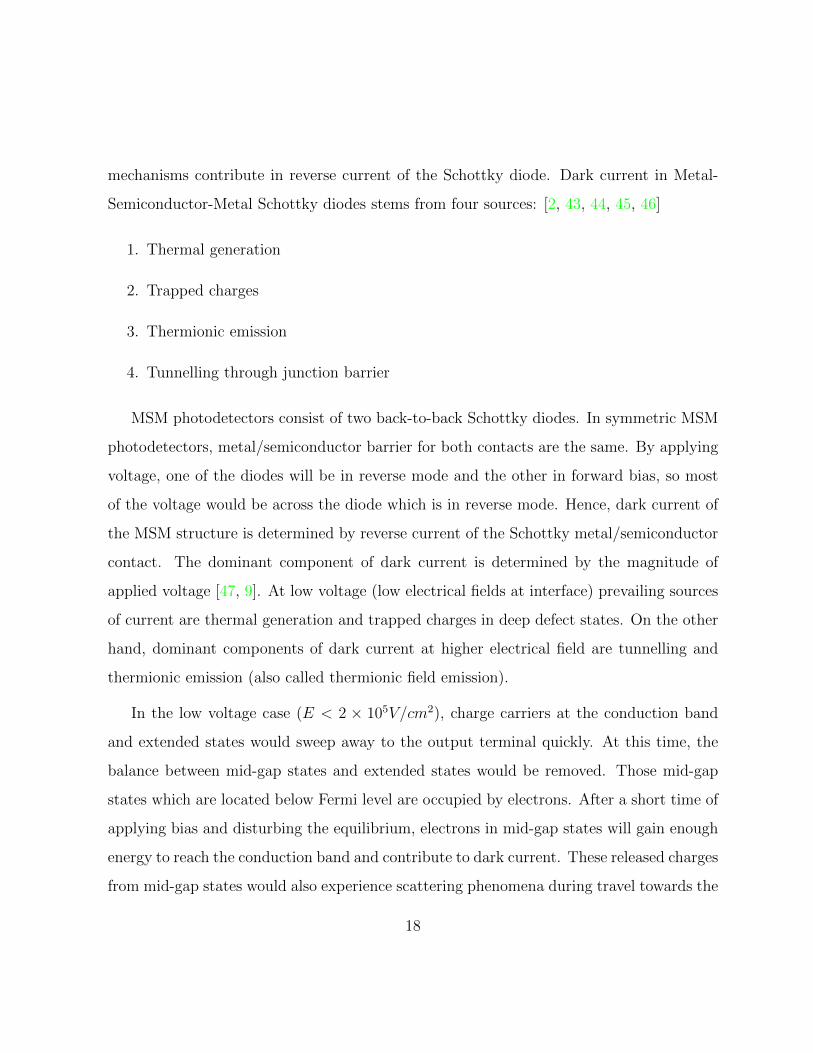
Figure 2.3: Electron transport in a-Si layer; F represents the electric field, Et, shows the Fermilevel in a-Si, and w is the depletion width. [6]
junction due to existence of localized states at the band tail of amorphous silicon. Therefore
transport of these charge carriers consists of multiple trapping and releasing to reach the
output terminal. This type of transport mechanism is called dispersive transport which is
fully described by H. Scher et al. and T. Tiedje et al. [7, 48]
Figure 2.3 describes the basics of dispersive transport mechanism. Briefly, in disper-
sive transport, sheets of charge carriers in the material would be extended while travelling
through the material (due to multiple trapping and releasing) and consequently the out-
put terminal senses current which is varying with time. Figure 2.4 demonstrates typical
transient current due to despersive transport [7].
As it can be seen, we have:
I ∝ t−α (2.1)
where α is related to trap state density. Hence, we can say that overall transient be-
haviour of dark current at low bias (no injection from electrodes) is due to the time needed
19
Figure 2.4: Transient current cause by dispersive transient. [6, 7]
to released trapped charges from mid-gap states, plus time it takes to reach the contact
terminal due to dispersive transport [47]. Also it’s worthwhile to note that dispersive
transport would also explain transient behaviour of the Schottky diodes after a short light
pulse based on rate of trap filling. We will briefly discuss this in following sections.
At steady state and in absence of injection from contacts, the dominant component of
dark current will be thermal generation of a-Si which can be shown as below [2],
Jth = eN(EqF )kTω0exp[−(EC − EqF )/kT ]Ad, (2.2)
where ω0 = 1013s−1 and EqF is quasi fermi level. N is density of trapped states which we
take as N = 1017cm−3eV −1, where A and d are area and thickness of the film respectively.
Also, for intrinsic amorphous silicon we have EC − EqF = 0.9eV [2] which would result in
a current of ≈ 1− 2pA/mm2 for detector with a 400nm i-layer.
20
By increasing the bias voltage (E > 2 ∗ 105V/cm), in addition to thermal generation,
thermal field emission and quantum mechanical tunnelling also contribute to dark current.
It has been understood that both of these mechanism strongly depend on width and height
of the barrier at the metal/semiconductor interface. It has been shown before that the
height of the barrier at the metal/amorphous silicon is fairly dependent on the metal work
function due to similar densities and energy distribution of surface state at the metal/a-Si
interface [49]. However width of the barrier is strongly dependent on electric field and
trapped charges at the interface and their release over time. These trapped charges at the
interface arise from dangling bonds and defect state in the mid-gap of amorphous silicon [2].
Instability of dark current in amorphous silicon based Schottky diodes has been attributed
to release of trapped charge at the interface over time [9]. This implies the fact that the
width of the Schottky barrier (which determines rate of tunnelling) changes over time due
to release of trapped charges at the interface until it reaches a steady state condition.
As mentioned, before applying voltage, at equilibrium condition, mid-gap states located
below Fermi level are occupied by electrons. By applying voltage, mobile carriers in the
conduction band and extended states would move towards junction barrier. During the
time that it takes trapped charges at mid-gap states to gain enough energy to reach the
conduction band, these trapped charges mask the depletion region and bulk of amorphous
silicon. Consequently band bending at the metal/a-Si interface would go further than its
steady state to bulk of amorphous silicon. Thus, at the moment of applying voltage to
the Schottky diode, the width of the barrier at the metal/a-Si would be larger than its
steady state, which means a lower chance of quantum mechanical tunnelling through the
barrier. As time elapses, those trapped charges which had masked the depletion region
would gradually release and reach to conduction band. As a result, depletion width shrinks
over time to steady state. Hence, after a few seconds of applying voltage, dark current
21
tends to increase.
A comprehensive study of reverse current in amorphous silicon based Schottky diode
was done by K. Aflatooni et al. [9]. According to K. Aflatooni et al. total current density
of reverse current in a-Si based Schottky diodes is described as:
Jtot = A∗T 2exp[−q (φ0 − a||E|| − a||E(t)||)kT
], (2.3)
where A∗ is Richardson’s constant, given by,
A∗ =4πqm∗k2
h3, (2.4)
which is ≈ 120A/(cm2K2) [2]. The tunnelling parameter a depends on effective mass,
dielectric constant and etc. T is temperature and E is as electric field which varies in time
due to the variation of barrier width at the interface.
Figures 4.3 presents instability of dark current in amorphous silicon base MSM pho-
todetector which were reported before. [9, 8].
22
Figure 2.5: Dark current instability under constant voltage over time. Reported by (a)Taghibakhsh et al. [8] (b) Aflatooni et al. [9].
2.3.2 Photocurrent
Photocurrent in all photodetectors determines the level of responsivity and efficiency of the
detector. Photocurrent in steady state arises from different mechanisms including drift,
diffusion and recombination of excess carriers. It’s been shown that at low electric field,
diffusion is the dominant component of photocurrent and by increasing the bias voltage,
drift of generated charges would dominant at steady state [50].
By assuming drift is the main component of photocurrent and no space-charge-limited
phenomena, we can drive photocurrent in steady state based on optical charge generation
[8, 51],
Jph = qGopµτrE, (2.5)
where Gop is optical generation, q is charge of electron, E is electric field (which we assumed
is constant in between electrode spacing) and µτr is mobility-lifetime product which is
23
dependent on electric field. We should note that due to optical refractive index differences
at the interface, some portion of light will reflect at the interface and that the thickness of
the active layer determines how much of incoming light will be absorbed. Hence, we can
write optical generation as:
Gop = (1−R)(1− exp(−αta−si))Popt
hνta−Si, (2.6)
where R is refelectivity, ta−Si is thickness of a-Si, Popt is power of incoming light and ν is
frequency of light. Consequently we would have current of a single MSM PD with gap of
L and width of W given as:
Iph = q(1−R)(1− exp(−αta−si))Popthν
µτVW
L. (2.7)
It should be noted that we consider infinite surface recombination at the contacts
and we neglect the effect of charge diffusion and recombination in the bulk of amorphous
silicon. Comprehensive study of photocurrent at steady state in lateral MSM structure
by 1D approximation is done by A. W. Sarto et al. [50]. However equation (2.7) implies
a linear relation between photon flux and photocurrent which is a critical property of
photodetectors. We should also consider that by increasing photon flux, we expect to see
sub-linear behaviour from the photodetector which can be explained by the effect of the
number of incoming photons to mobility-lifetime product [52].
2.3.3 Capacitance
Generally coplanar metal-semiconductor-metal photodetectors are well-known for their low
capacitance in compare to vertical p-i-n photodiodes and consequently lower charge and
24
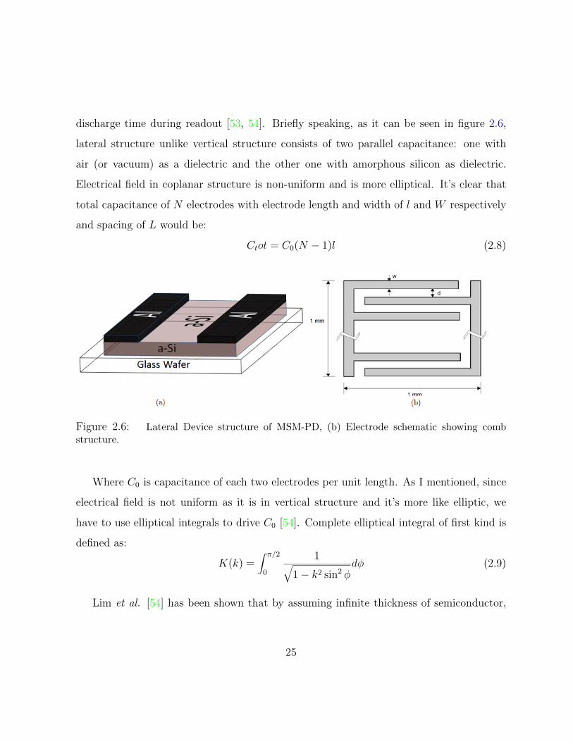
discharge time during readout [53, 54]. Briefly speaking, as it can be seen in figure 2.6,
lateral structure unlike vertical structure consists of two parallel capacitance: one with
air (or vacuum) as a dielectric and the other one with amorphous silicon as dielectric.
Electrical field in coplanar structure is non-uniform and is more elliptical. It’s clear that
total capacitance of N electrodes with electrode length and width of l and W respectively
and spacing of L would be:
Ctot = C0(N − 1)l (2.8)
Figure 2.6: Lateral Device structure of MSM-PD, (b) Electrode schematic showing combstructure.
Where C0 is capacitance of each two electrodes per unit length. As I mentioned, since
electrical field is not uniform as it is in vertical structure and it’s more like elliptic, we
have to use elliptical integrals to drive C0 [54]. Complete elliptical integral of first kind is
defined as:
K(k) =∫ π/2
0
1√1− k2 sin2 φ
dφ (2.9)
Lim et al. [54] has been shown that by assuming infinite thickness of semiconductor,
25
C0 is given by
C0 = ε0(1 + εs)K(k)
K(k‘)(2.10)
where
k = tan2 π
4
L
W + L(2.11)
and
k‘ = 1− k2 (2.12)
2.3.4 Dynamic Range
Dynamic range is one of the most critical factor that determines performance of detectors,
specially in medical imaging application where lower dose to the patient is matter of inter-
est. Dynamic rang as detection point of view defines as the range of incoming photon flux
that is detectable by detector. It is obvious that dark current of the detector or readout
electronic noise determines lower limit of dynamic range. On the other hand, as readout
point of view, especially in integration mode , dynamic rang defines as a ability of pixel
detector in accumulating charges during integration. Figure 2.7 demonstrate a simple PPS
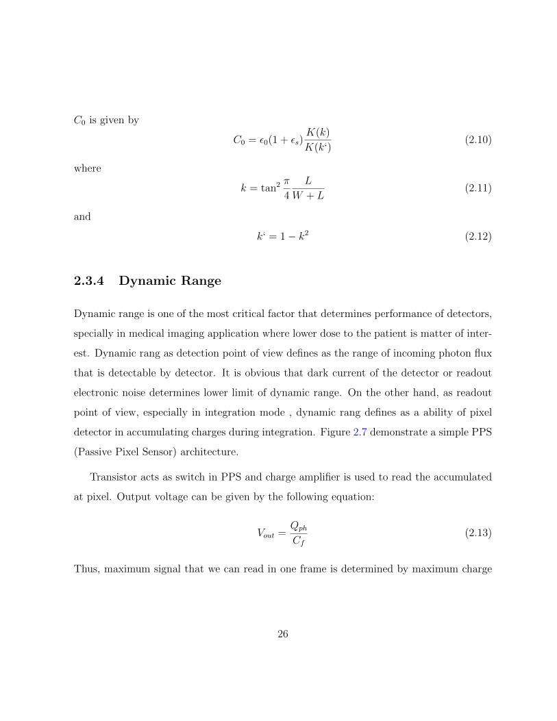
(Passive Pixel Sensor) architecture.
Transistor acts as switch in PPS and charge amplifier is used to read the accumulated
at pixel. Output voltage can be given by the following equation:
Vout =Qph
Cf(2.13)
Thus, maximum signal that we can read in one frame is determined by maximum charge
26
Figure 2.7: Lateral PPS architecture using a-Si detector for digital imaging
that can be accumulated by pixel capacitance. For the maximum charge we have
Qph−max = Vpix−max.Cdet (2.14)
Vpix−max is determined by working range of detector in term of applied voltage. In conven-
tional p-i-n detector which is widely used in indirect medical imaging, the rang of applied
bias to the detector is around 5− 10V (due to breakdown point). By considering the fact
that detector should maintain its linearity behaviour in integration mode, the maximum
swing of voltage across detector is going to be 250 − 500mV . Hence, by having a ability
to operate detector in high voltage biases, we will improve dynamic range of the detector
in integration mode imaging.
27
Chapter 3
Experimental and Instrumental
Methodology
Advantages of amorphous silicon stem from its radiation resistivity, suitability in fabri-
cation and integration with large area flat panels and film uniformity. First, the device
structure and process aspects involved with the fabrication of both vertical and lateral a-Si
MSM photodetectors are presented in this chapter, followed by various characterization
techniques that were used in this research. The fabrication process for lateral and vertical
structures takes a 2 and 3 day run respectively based on how the facility operates at that
time and the success of each step goes.
3.1 Fabrication Process
Fabrication of the proposed MSM photodetector consists of following process:
• Wafer cleaning and substrate preparation
28
• Preparation of thin polyimide solution
• Amorphous silicon deposition
• Spin coating of desired polyimide layer (twice for the vertical structure)
• Aluminium magnetron sputtering
• Photo-lithography (required for the lateral structure)
3.1.1 Wafer preparing
High quality deposition of amorphous silicon film requires a clean substrate clear of any
contamination such as dust, organic particles, oil, etc. Two different substrates were
used in the course of this work: uncoated Corning 7059 type glass (high resistivity) and
Corning 1737F glass with one surface coated with a 50nm ITO (indium tin oxide) layer
for lateral and vertical structure respectively. Regarding the uncoated glass wafer, the
cleaning process starts with a typical RCA type 1 to remove organic residue and films.
This is followed by ultrasonica bath substrate cleaning with Acetone and Propanol for
approximately 5 minutes each. Finally, substrates are dried by using purified Nitrogen gas
for about 2 minutes. In the case of ITO coated glass, the cleaning process only includes
ultrasonic cleaning with Acetone and Propanol for 15 minutes each and drying.
3.1.2 a-Si deposition
The performance of the proposed MSM photodetector depends strongly on the quality
of amorphous silicon which acts as an active layer in the device. The usual method of
depositing intrinsic a-Si is by plasma decomposition of Silane gas (SiH4). Typically, in
29
absence of plasma, silane decomposes at the temperature of above 450C which result in poor
quality amorphous silicon film (the high temperature of the substrate prevents hydrogen
retention) [2]. An intrinsic a-Si layer for the lateral structure has been deposited using
a plasma enhancement chemical vapour deposition (PECVD) cluster tool system. This
cluster tool is multi-chambered and has a dedicated chamber for intrinsic a-Si capable
of pumping down to 1E − 8 Torr. Substrate temperature is controlled by a heater flush
with the substrate and the RF deposition system is capacitively coupled parallel plate RF
(13.56MHz). During deposition, the substrate faces down in the chamber. Amorphous
silicon was deposited at 250C using pure SiH4 (no hydrogen dilution).
Due to limitations with the PECVD cluster tool, we weren’t able to deposit the i-layer
for the vertical structure with the same system and recipe that we used for the lateral
structure. As mentioned, in the PECVD cluster tool, during deposition the substrate is
facing down. In the lateral structure, since the substrate is uncoated corning glass, this
won’t cause a problem. However, for the vertical structure -where a-Si is sandwiched
between two thin polyimide layers- the substrate is ITO coated glass with cured polyimide
coated on it. Since the deposition is happening at 250C, by putting the ITO substrate with
polyimide inside the PECVD cluster tool chamber, the risk of polyimide peeling off to the
chamber is high. In courtesy of other lab users and to avoid contamination, I switched to
a single chamber Plasma Therm VII PECVD system (Substrate faces up in this machine).
3.1.3 Thin Polyimide
Polyimide is a well-known insulator in CMOS fabrication. Recently, there has been several
studies on polyimide conduction mechanisms at high electric field [conduction PI] as well
as using polyimide as a blocking layer to prevent injection of carriers into the active layer
30
[13]. Polyimide is available commercially in both sheets (needs only curing process) and
solution (needs spin coating and curing process). In this research we have used polyimide in
solvent. 1µm polyimide is reported as a blocking layer for a-Se MSM structures [13]. Since
resistivity and thickness of the proposed a-Si base MSM-PD is lower than the previously
reported a-Se MSM-PD, polyimide films with a thickness of equal or less than 300nm was
needed. The least viscose polyimide solution that is available commercially is PI 2610 from
HD-MicroSystems. The coating process for this type of polyimide is spin coating and the
thickness of the film is determined by RPM. As it is mentioned in PI 2610 data sheet,
the thickness of the film is going to saturate at at 5000rpm which leads to a minimum
thickness of 800nm− 1µm. In order to spin coat thin polyimide, I dilute the solution with
adhesion promoter T-9038 with equal volume weight. Some points should be considered
during the making of a thin polyimide solution, otherwise film quality after spin coating
and curing would be likely poor.
• Polyimide should be kept inside freezer (between -10 to -18C) and before using it,
it is necessary to wait untill solution temperature reaches room temperature other-
wise humanity will diffuse into polyimide. Moisture contamination is detrimental to
polyimide stability and must be avoided based on datasheet.
• First certain amount of polyimide (i.e 3 − 6ml) should be poured into clean bottle
(preferably no syringe used), followed by adding known amount of adhesion promoter
(T-9038) (i.e 3− 6ml).
• In order to mix the solution, any kind of quick movement should be avoided to prevent
creation bubbles inside the solution. It is recommended to turn bottle rotated very
gently for about 3-4 minutes.
31
• The thinned solution should be allowed to age 12 hours at room temperature (20 C,
70 F) before use. This time is needed for the solution to reach equilibrium condition.
To coat around 150 ± 25nm polyimide, spin coating at speed of 5 krpm is needed for
30 sec. Table 3.1 shows spin coating steps and condition.
Table 3.1: PI spin coating process steps
Duration(sec) Speed (rpm) Acceleration (rpm/sec)
Step 1 7 500 250Step 2 35 5000 1000
After spin coating, in order to vaporize the solvent we carry out two prebaking steps
and one curing step which are described in tables 3.2 and 3.3 respectively.
Table 3.2: Pre-baking process
Duration(sec) Temperature (C)
Step 1 90 90Step 2 90 150
Table 3.3: Curing process
Duration(hr) Temperature (C) Ramp (C/hr)
2 350 240
3.1.4 Electrodes
In both the lateral and vertical structure, the last step of fabrication is sputtering and
patterning electrodes. Aluminium has been chosen as a metal electrode. In the vertical
case, since the area of a single pixel device is big (1mm2), no photo-lithography is needed
32
and pattering can be done by using shadow masks. In the lateral structure, patterning
electrodes is an unavoidable step. MA6 was used for the lithography step. Different device
configurations have been designed to understand performance of the detector.
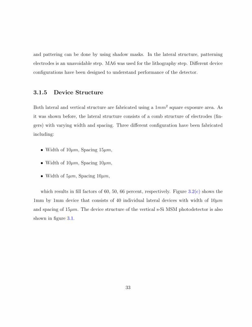
3.1.5 Device Structure
Both lateral and vertical structure are fabricated using a 1mm2 square exposure area. As
it was shown before, the lateral structure consists of a comb structure of electrodes (fin-
gers) with varying width and spacing. Three different configuration have been fabricated
including:
• Width of 10µm, Spacing 15µm,
• Width of 10µm, Spacing 10µm,
• Width of 5µm, Spacing 10µm,
which results in fill factors of 60, 50, 66 percent, respectively. Figure 3.2(c) shows the
1mm by 1mm device that consists of 40 individual lateral devices with width of 10µm
and spacing of 15µm. The device structure of the vertical s-Si MSM photodetector is also
shown in figure 3.1.
33
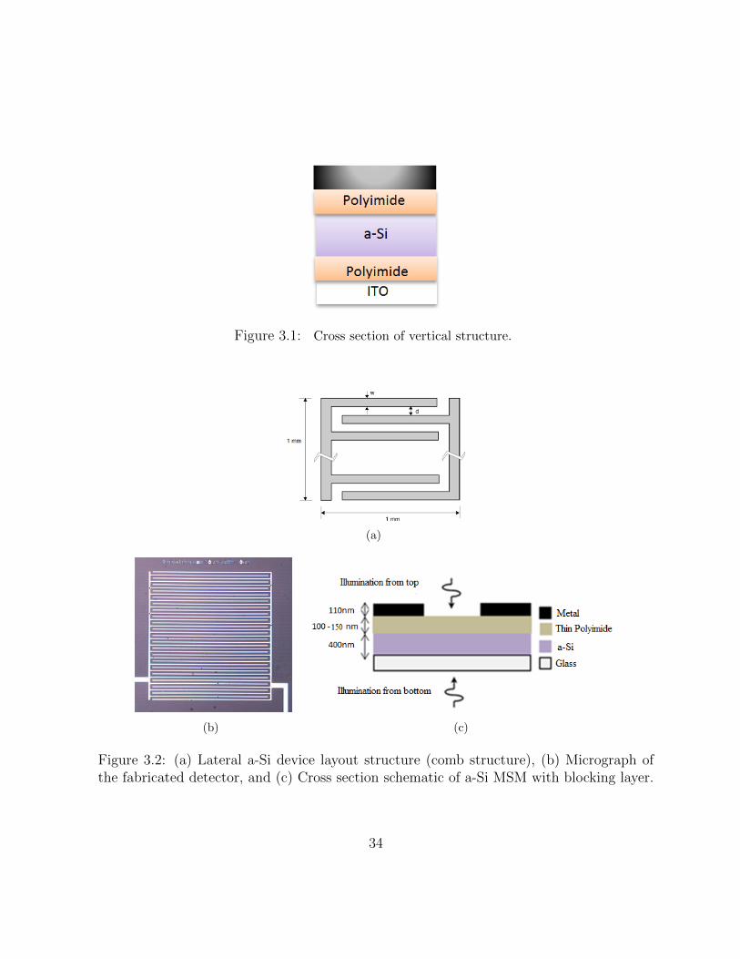
Figure 3.1: Cross section of vertical structure.
(a)
(b) (c)
Figure 3.2: (a) Lateral a-Si device layout structure (comb structure), (b) Micrograph ofthe fabricated detector, and (c) Cross section schematic of a-Si MSM with blocking layer.
34
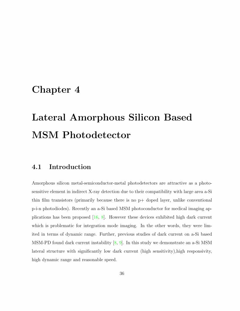
3.2 Characterization Techniques
MSM photodetector performance is characterized by dark current, dark current stability,
external quantum efficiency, responsitivity, linearity to incident photon flux and tempo-
ral response. In this work, dark current and photoresponse was recorded by an Agilent
Semiconductor Parameter Analyser (4156C) and low-noise micro-probe station. Regard-
ing biasing the device, a Stanford Research Systems PS350 high-voltage power supply was
used. Illumination happened from the bottom and top with a monochromatic LED (green,
blue and red). Intensity of incident light was also measured using a Newport 1935-R op-
tical power meter. Also MEDICI (Synopsis Inc.) was used to simulate and estimate the
electric field within the a-Si layer. Since the Agilent Semiconductor Parameter Analyser
is too slow for transient measurements, another set-up was used to record the transient
response of the detector. The measurement set-up that was used for temporal response of
the device is described in figure 3.3 which consists of a Ametek 5182 low-noise current to
voltage amplifier and fast digital oscilloscope.
Figure 3.3: Experimental set-up for time response measurment.
35
Chapter 4
Lateral Amorphous Silicon Based
MSM Photodetector
4.1 Introduction
Amorphous silicon metal-semiconductor-metal photodetectors are attractive as a photo-
sensitive element in indirect X-ray detection due to their compatibility with large area a-Si
thin film transistors (primarily because there is no p+ doped layer, unlike conventional
p-i-n photodiodes). Recently an a-Si based MSM photoconductor for medical imaging ap-
plications has been proposed [16, 8]. However these devices exhibited high dark current
which is problematic for integration mode imaging. In the other words, they were lim-
ited in terms of dynamic range. Further, previous studies of dark current on a-Si based
MSM-PD found dark current instability [8, 9]. In this study we demonstrate an a-Si MSM
lateral structure with significantly low dark current (high sensitivity),high responsivity,
high dynamic range and reasonable speed.
36
Figure 4.1: Lateral MSM a-Si:H device structure (left) and lateral MSM a.Si:H with blockinglayer (right). As you can see we have both option of lighting from top and bottom. Thin PI canbe considered transparent for green light.
In this chapter, as a base line, performance of a simple in house fabricated a-Si MSM
structure (figure 4.1 left) was investigated in terms of dark current, photoresponse and
responsivity. This structure is similar to previously studied a-Si MSM-PD [16, 8]. This
is followed by a comprehensive characterization and development of a high performance
MSM lateral structure with low and stable dark current. The improvements of the proposed
structure in terms of dark current and stability are achieved by the introduction of a thin
polymer layer as a blocking layer. Figure 4.1 demonstrates two lateral MSM structures.
4.2 Lateral a-Si MSM (without blocking layer)
4.2.1 Dark Current and its instability
In this section the performance of the a-Si MSM lateral photodetector (without blocking
layer) is going to be investigated. As mentioned in the second chapter, MSM photodetectors
consist of two back to back Schottky diodes and since the proposed structure is symmetric,
by applying voltage results in one being in reverse mode and the other in forward mode.
37
Therefore, dark current of MSM-PD is controlled by reverse current of the a-Si Schottky
diode. It is understood that dark current in MSM diodes stems from two mechanisms:
thermionic emission and tunnelling (at medium bias voltage range). Both strongly depend
on width and height of the barrier at metal/semiconductor interface. It has been shown
before that the height of the barrier at the metal/amorphous Si is fairly dependent on
the metal work function due to similar densities and energy distribution of surface states
at the metal/a-Si interface for different metals [49]. This implies that by increasing the
voltage across MSM-PD, a dramatic increase in dark current is expected since at medium
rage electric field (> 2 × 10⁵V/cm), dark current is controlled by quantum mechanical
tunnelling which is highly dependent to the field at barrier rather than thermal generation
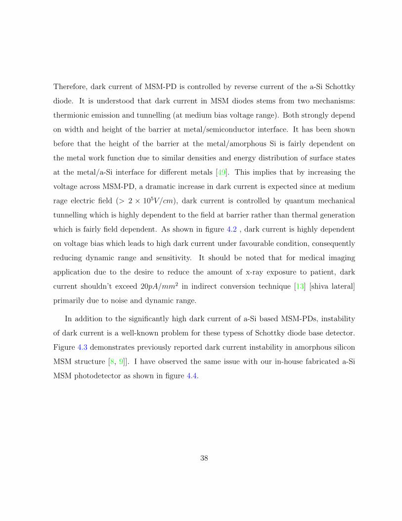
which is fairly field dependent. As shown in figure 4.2 , dark current is highly dependent
on voltage bias which leads to high dark current under favourable condition, consequently
reducing dynamic range and sensitivity. It should be noted that for medical imaging
application due to the desire to reduce the amount of x-ray exposure to patient, dark
current shouldn’t exceed 20pA/mm2 in indirect conversion technique [13] [shiva lateral]
primarily due to noise and dynamic range.
In addition to the significantly high dark current of a-Si based MSM-PDs, instability
of dark current is a well-known problem for these typess of Schottky diode base detector.
Figure 4.3 demonstrates previously reported dark current instability in amorphous silicon
MSM structure [8, 9]]. I have observed the same issue with our in-house fabricated a-Si
MSM photodetector as shown in figure 4.4.
38
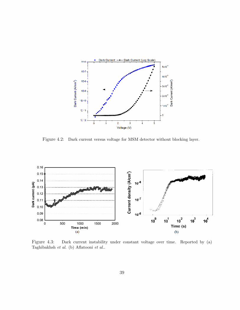
Figure 4.2: Dark current versus voltage for MSM detector without blocking layer.
Figure 4.3: Dark current instability under constant voltage over time. Reported by (a)Taghibakhsh et al. (b) Aflatooni et al..
39
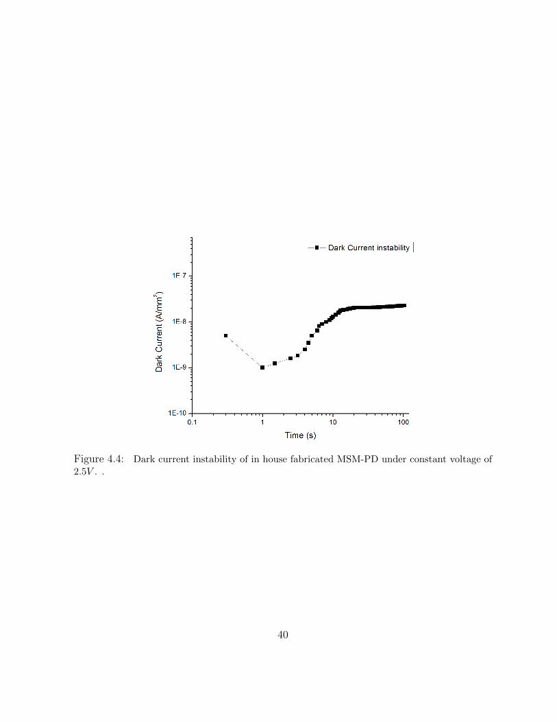
Figure 4.4: Dark current instability of in house fabricated MSM-PD under constant voltage of2.5V . .
40
4.2.2 Photoresponse
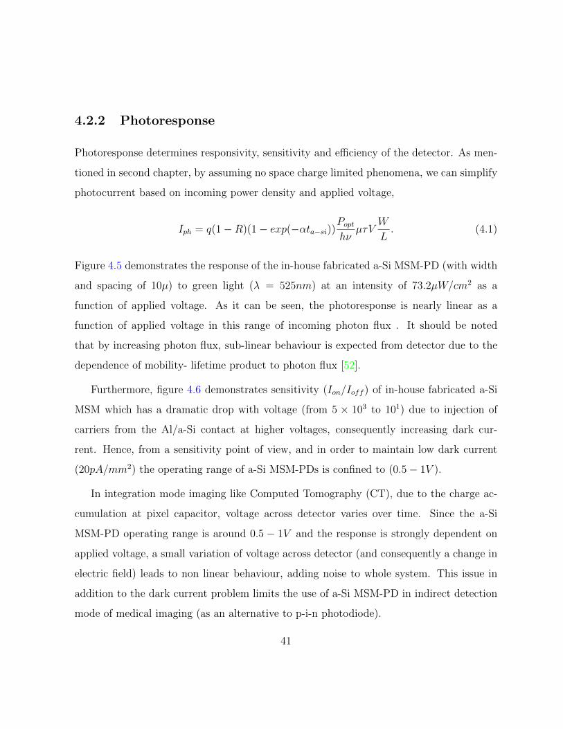
Photoresponse determines responsivity, sensitivity and efficiency of the detector. As men-
tioned in second chapter, by assuming no space charge limited phenomena, we can simplify
photocurrent based on incoming power density and applied voltage,
Iph = q(1−R)(1− exp(−αta−si))Popthν
µτVW
L. (4.1)
Figure 4.5 demonstrates the response of the in-house fabricated a-Si MSM-PD (with width
and spacing of 10µ) to green light (λ = 525nm) at an intensity of 73.2µW/cm2 as a
function of applied voltage. As it can be seen, the photoresponse is nearly linear as a
function of applied voltage in this range of incoming photon flux . It should be noted
that by increasing photon flux, sub-linear behaviour is expected from detector due to the
dependence of mobility- lifetime product to photon flux [52].
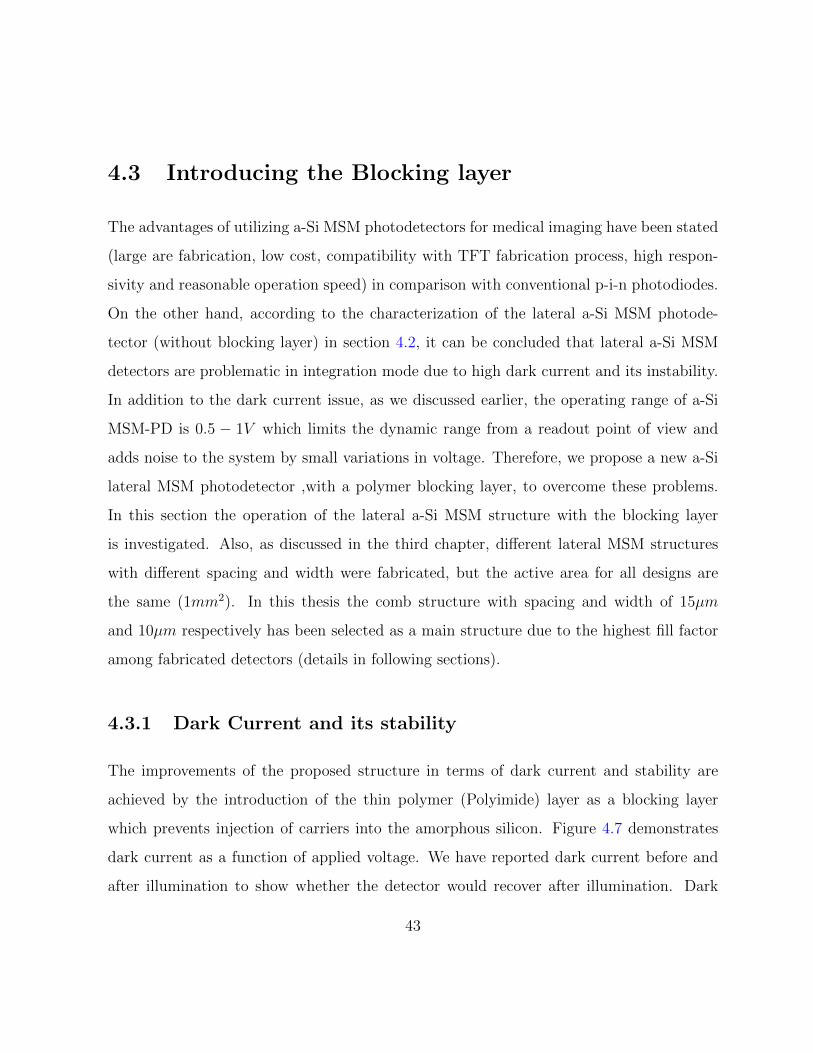
Furthermore, figure 4.6 demonstrates sensitivity (Ion/Ioff ) of in-house fabricated a-Si
MSM which has a dramatic drop with voltage (from 5 × 10³ to 101) due to injection of
carriers from the Al/a-Si contact at higher voltages, consequently increasing dark cur-
rent. Hence, from a sensitivity point of view, and in order to maintain low dark current
(20pA/mm2) the operating range of a-Si MSM-PDs is confined to (0.5− 1V ).
In integration mode imaging like Computed Tomography (CT), due to the charge ac-
cumulation at pixel capacitor, voltage across detector varies over time. Since the a-Si
MSM-PD operating range is around 0.5 − 1V and the response is strongly dependent on
applied voltage, a small variation of voltage across detector (and consequently a change in
electric field) leads to non linear behaviour, adding noise to whole system. This issue in
addition to the dark current problem limits the use of a-Si MSM-PD in indirect detection
mode of medical imaging (as an alternative to p-i-n photodiode).
41
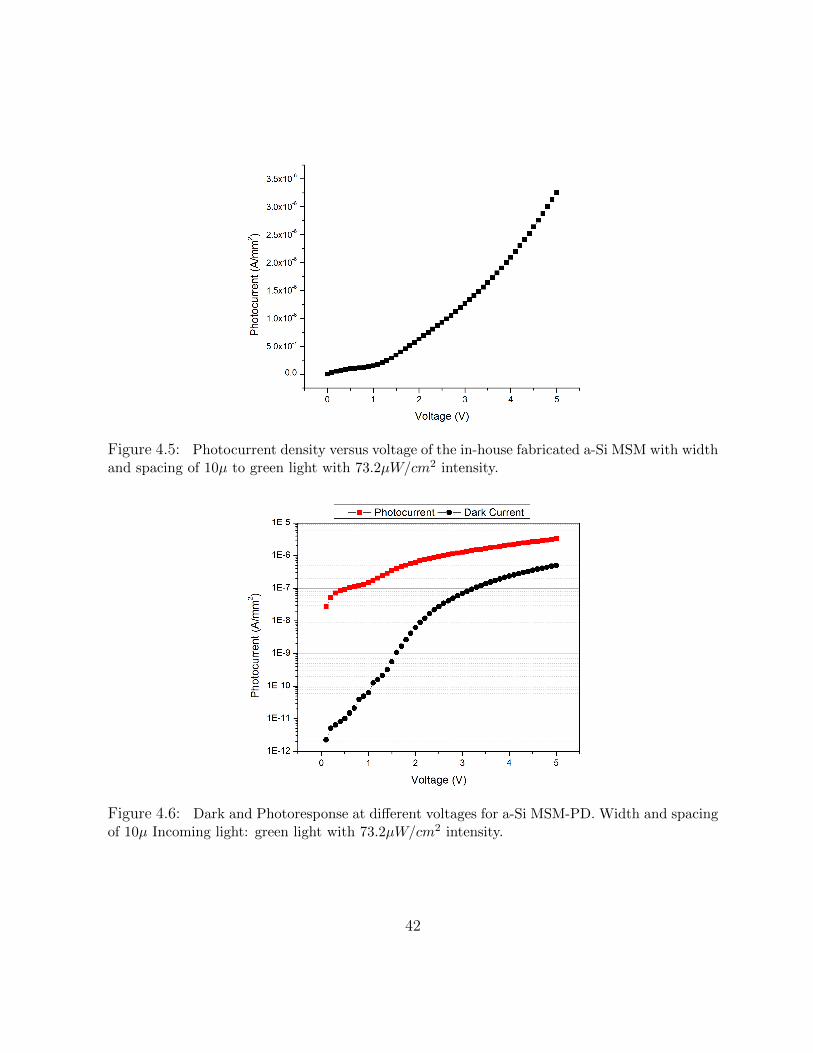
Figure 4.5: Photocurrent density versus voltage of the in-house fabricated a-Si MSM with widthand spacing of 10µ to green light with 73.2µW/cm2 intensity.
Figure 4.6: Dark and Photoresponse at different voltages for a-Si MSM-PD. Width and spacingof 10µ Incoming light: green light with 73.2µW/cm2 intensity.
42
4.3 Introducing the Blocking layer
The advantages of utilizing a-Si MSM photodetectors for medical imaging have been stated
(large are fabrication, low cost, compatibility with TFT fabrication process, high respon-
sivity and reasonable operation speed) in comparison with conventional p-i-n photodiodes.
On the other hand, according to the characterization of the lateral a-Si MSM photode-
tector (without blocking layer) in section 4.2, it can be concluded that lateral a-Si MSM
detectors are problematic in integration mode due to high dark current and its instability.
In addition to the dark current issue, as we discussed earlier, the operating range of a-Si
MSM-PD is 0.5 − 1V which limits the dynamic range from a readout point of view and
adds noise to the system by small variations in voltage. Therefore, we propose a new a-Si
lateral MSM photodetector ,with a polymer blocking layer, to overcome these problems.
In this section the operation of the lateral a-Si MSM structure with the blocking layer
is investigated. Also, as discussed in the third chapter, different lateral MSM structures
with different spacing and width were fabricated, but the active area for all designs are
the same (1mm2). In this thesis the comb structure with spacing and width of 15µm
and 10µm respectively has been selected as a main structure due to the highest fill factor
among fabricated detectors (details in following sections).
4.3.1 Dark Current and its stability
The improvements of the proposed structure in terms of dark current and stability are
achieved by the introduction of the thin polymer (Polyimide) layer as a blocking layer
which prevents injection of carriers into the amorphous silicon. Figure 4.7 demonstrates
dark current as a function of applied voltage. We have reported dark current before and
after illumination to show whether the detector would recover after illumination. Dark
43
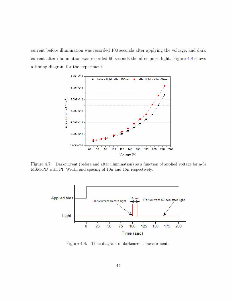
current before illumination was recorded 100 seconds after applying the voltage, and dark
current after illumination was recorded 60 seconds the after pulse light. Figure 4.8 shows
a timing diagram for the experiment.
Figure 4.7: Darkcurrent (before and after illumination) as a function of applied voltage for a-SiMSM-PD with PI. Width and spacing of 10µ and 15µ respectively.
Figure 4.8: Time diagram of darkcurrent measurment.
44
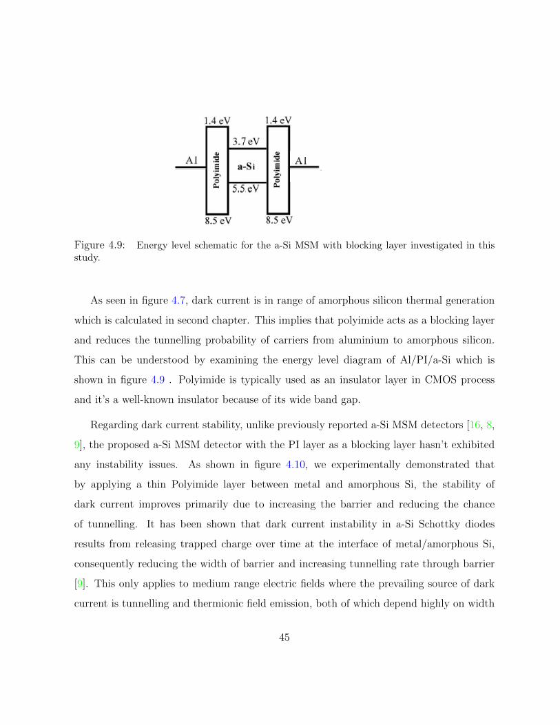
Figure 4.9: Energy level schematic for the a-Si MSM with blocking layer investigated in thisstudy.
As seen in figure 4.7, dark current is in range of amorphous silicon thermal generation
which is calculated in second chapter. This implies that polyimide acts as a blocking layer
and reduces the tunnelling probability of carriers from aluminium to amorphous silicon.
This can be understood by examining the energy level diagram of Al/PI/a-Si which is
shown in figure 4.9 . Polyimide is typically used as an insulator layer in CMOS process
and it’s a well-known insulator because of its wide band gap.
Regarding dark current stability, unlike previously reported a-Si MSM detectors [16, 8,
9], the proposed a-Si MSM detector with the PI layer as a blocking layer hasn’t exhibited
any instability issues. As shown in figure 4.10, we experimentally demonstrated that
by applying a thin Polyimide layer between metal and amorphous Si, the stability of
dark current improves primarily due to increasing the barrier and reducing the chance
of tunnelling. It has been shown that dark current instability in a-Si Schottky diodes
results from releasing trapped charge over time at the interface of metal/amorphous Si,
consequently reducing the width of barrier and increasing tunnelling rate through barrier
[9]. This only applies to medium range electric fields where the prevailing source of dark
current is tunnelling and thermionic field emission, both of which depend highly on width
45
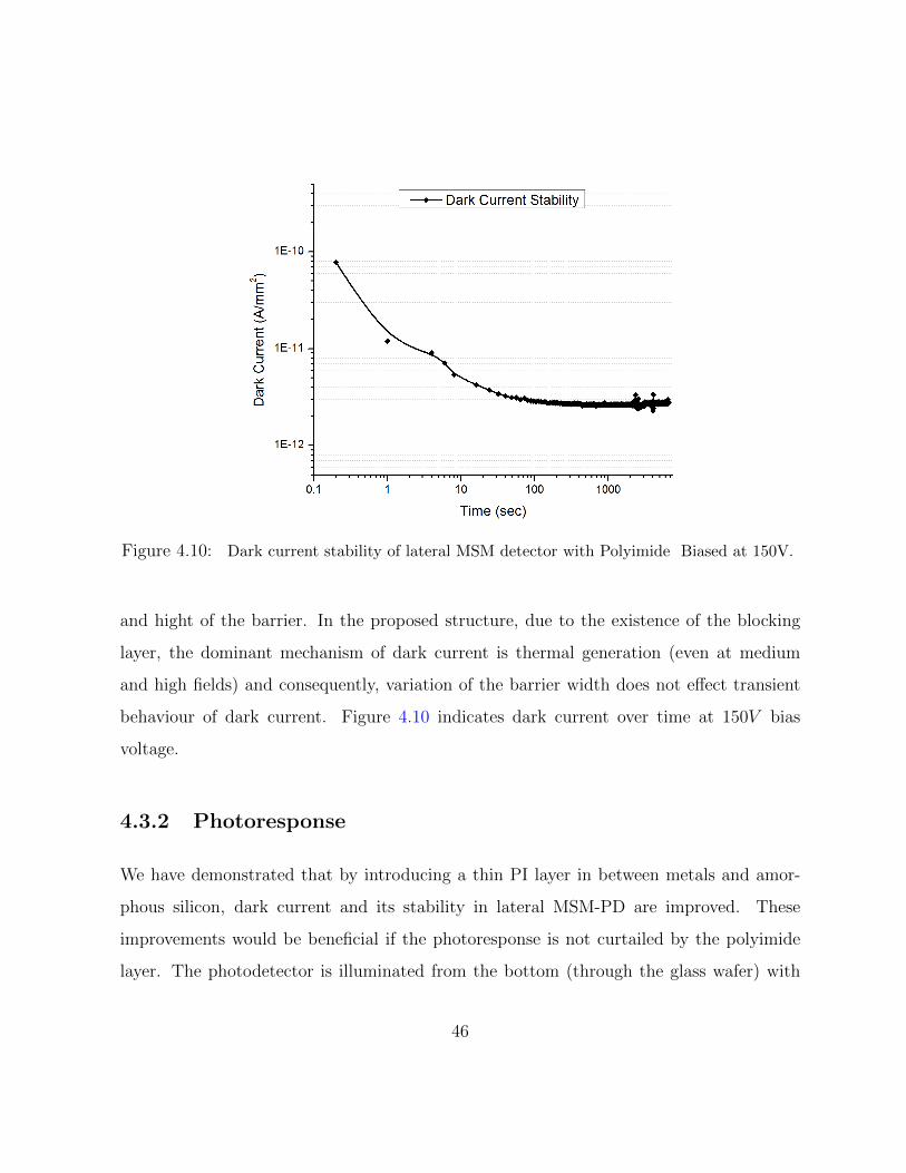
Figure 4.10: Dark current stability of lateral MSM detector with Polyimide Biased at 150V.
and hight of the barrier. In the proposed structure, due to the existence of the blocking
layer, the dominant mechanism of dark current is thermal generation (even at medium
and high fields) and consequently, variation of the barrier width does not effect transient
behaviour of dark current. Figure 4.10 indicates dark current over time at 150V bias
voltage.
4.3.2 Photoresponse
We have demonstrated that by introducing a thin PI layer in between metals and amor-
phous silicon, dark current and its stability in lateral MSM-PD are improved. These
improvements would be beneficial if the photoresponse is not curtailed by the polyimide
layer. The photodetector is illuminated from the bottom (through the glass wafer) with
46
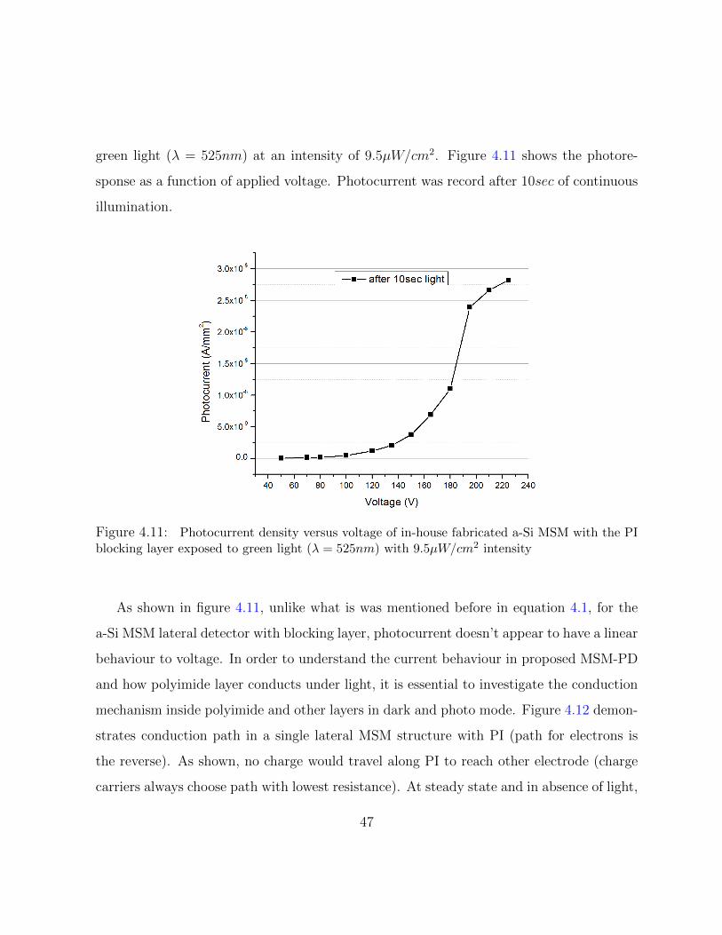
green light (λ = 525nm) at an intensity of 9.5µW/cm2. Figure 4.11 shows the photore-
sponse as a function of applied voltage. Photocurrent was record after 10sec of continuous
illumination.
Figure 4.11: Photocurrent density versus voltage of in-house fabricated a-Si MSM with the PIblocking layer exposed to green light (λ = 525nm) with 9.5µW/cm2 intensity
As shown in figure 4.11, unlike what is was mentioned before in equation 4.1, for the
a-Si MSM lateral detector with blocking layer, photocurrent doesn’t appear to have a linear
behaviour to voltage. In order to understand the current behaviour in proposed MSM-PD
and how polyimide layer conducts under light, it is essential to investigate the conduction
mechanism inside polyimide and other layers in dark and photo mode. Figure 4.12 demon-
strates conduction path in a single lateral MSM structure with PI (path for electrons is
the reverse). As shown, no charge would travel along PI to reach other electrode (charge
carriers always choose path with lowest resistance). At steady state and in absence of light,
47
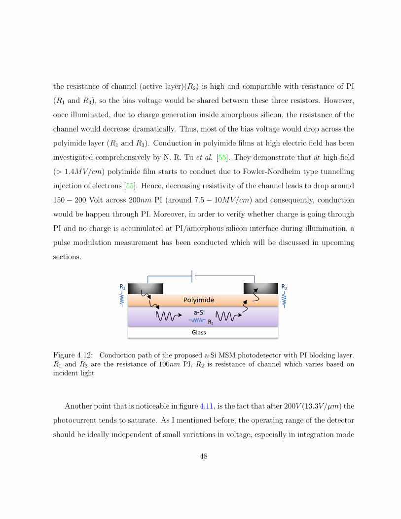
the resistance of channel (active layer)(R2) is high and comparable with resistance of PI
(R1 and R3), so the bias voltage would be shared between these three resistors. However,
once illuminated, due to charge generation inside amorphous silicon, the resistance of the
channel would decrease dramatically. Thus, most of the bias voltage would drop across the
polyimide layer (R1 and R3). Conduction in polyimide films at high electric field has been
investigated comprehensively by N. R. Tu et al. [55]. They demonstrate that at high-field
(> 1.4MV/cm) polyimide film starts to conduct due to Fowler-Nordheim type tunnelling
injection of electrons [55]. Hence, decreasing resistivity of the channel leads to drop around
150 − 200 Volt across 200nm PI (around 7.5 − 10MV/cm) and consequently, conduction
would be happen through PI. Moreover, in order to verify whether charge is going through
PI and no charge is accumulated at PI/amorphous silicon interface during illumination, a
pulse modulation measurement has been conducted which will be discussed in upcoming
sections.
Figure 4.12: Conduction path of the proposed a-Si MSM photodetector with PI blocking layer.R1 and R3 are the resistance of 100nm PI, R2 is resistance of channel which varies based onincident light
Another point that is noticeable in figure 4.11, is the fact that after 200V (13.3V/µm) the
photocurrent tends to saturate. As I mentioned before, the operating range of the detector
should be ideally independent of small variations in voltage, especially in integration mode
48
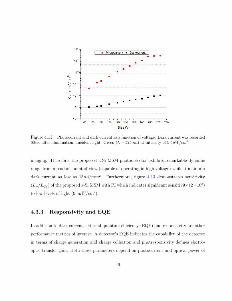
Figure 4.13: Photocurrent and dark current as a function of voltage. Dark current was recorded60sec after illumination. Incident light: Green (λ = 525nm) at intensity of 9.5µW/cm2
imaging. Therefore, the proposed a-Si MSM photodetector exhibits remarkable dynamic
range from a readout point of view (capable of operating in high voltage) while it maintain
dark current as low as 15pA/mm2. Furthermore, figure 4.13 demonstrates sensitivity
(Ion/Ioff ) of the proposed a-Si MSM with PI which indicates significant sensitivity (2×10³)
to low levels of light (9.5µW/cm2).
4.3.3 Responsivity and EQE
In addition to dark current, external quantum efficiency (EQE) and responsivity are other
performance metrics of interest. A detector’s EQE indicates the capability of the detector
in terms of charge generation and charge collection and photresponsivity defines electro-
optic transfer gain. Both these parameters depend on photocurrent and optical power of
49
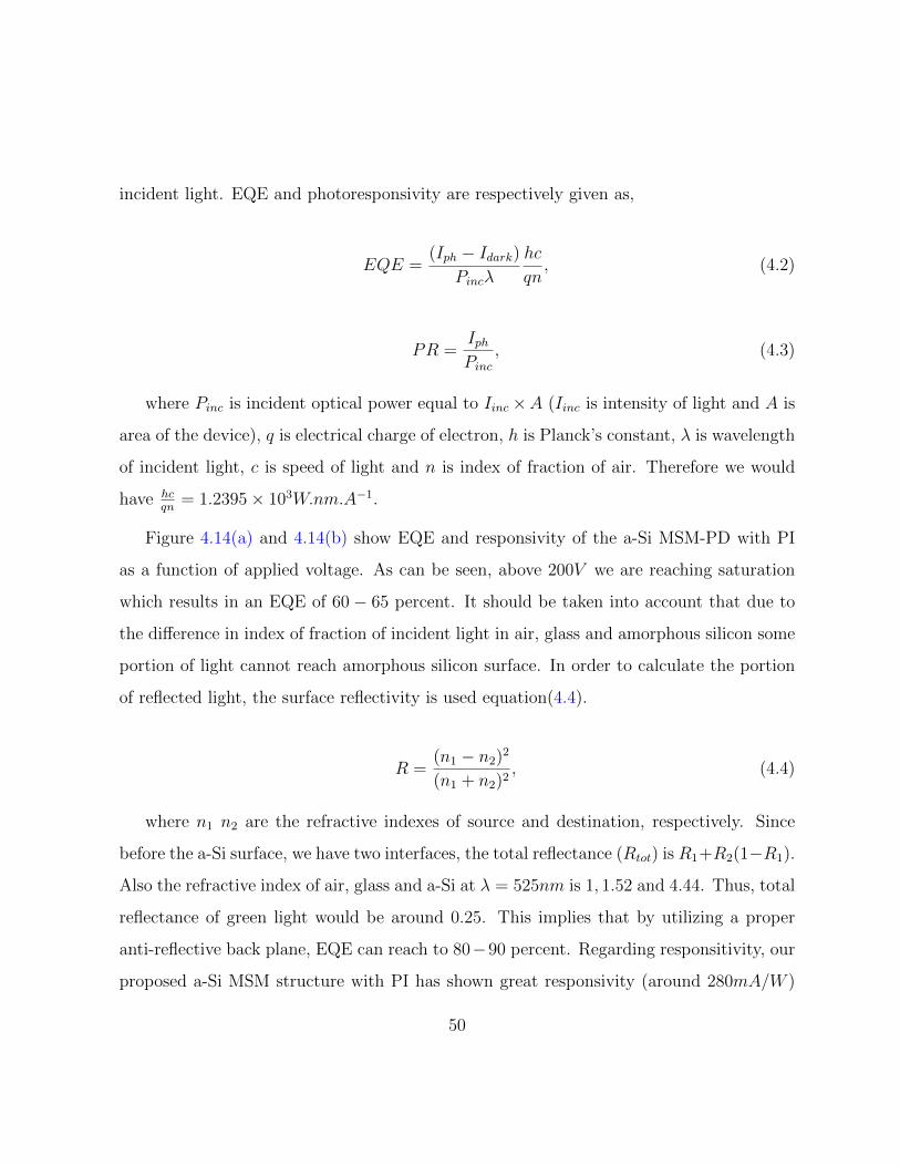
incident light. EQE and photoresponsivity are respectively given as,
EQE =(Iph − Idark)
Pincλ
hc
qn, (4.2)
PR =IphPinc
, (4.3)
where Pinc is incident optical power equal to Iinc×A (Iinc is intensity of light and A is
area of the device), q is electrical charge of electron, h is Planck’s constant, λ is wavelength
of incident light, c is speed of light and n is index of fraction of air. Therefore we would
have hcqn
= 1.2395× 10³W.nm.A−1.
Figure 4.14(a) and 4.14(b) show EQE and responsivity of the a-Si MSM-PD with PI
as a function of applied voltage. As can be seen, above 200V we are reaching saturation
which results in an EQE of 60 − 65 percent. It should be taken into account that due to
the difference in index of fraction of incident light in air, glass and amorphous silicon some
portion of light cannot reach amorphous silicon surface. In order to calculate the portion
of reflected light, the surface reflectivity is used equation(4.4).
R =(n1 − n2)
2
(n1 + n2)2, (4.4)
where n1 n2 are the refractive indexes of source and destination, respectively. Since
before the a-Si surface, we have two interfaces, the total reflectance (Rtot) is R1+R2(1−R1).
Also the refractive index of air, glass and a-Si at λ = 525nm is 1, 1.52 and 4.44. Thus, total
reflectance of green light would be around 0.25. This implies that by utilizing a proper
anti-reflective back plane, EQE can reach to 80−90 percent. Regarding responsitivity, our
proposed a-Si MSM structure with PI has shown great responsivity (around 280mA/W )
50
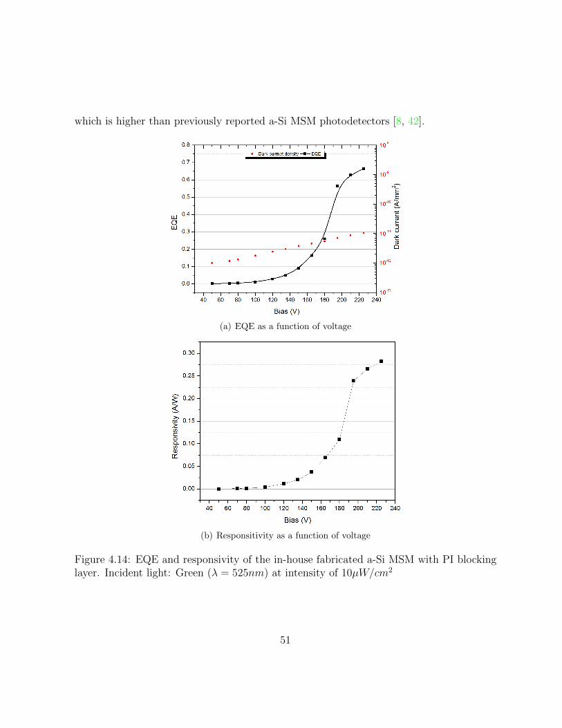
which is higher than previously reported a-Si MSM photodetectors [8, 42].
(a) EQE as a function of voltage
(b) Responsitivity as a function of voltage
Figure 4.14: EQE and responsivity of the in-house fabricated a-Si MSM with PI blockinglayer. Incident light: Green (λ = 525nm) at intensity of 10µW/cm2
51
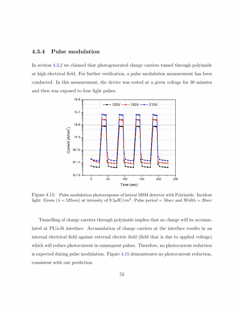
4.3.4 Pulse modulation
In section 4.3.2 we claimed that photogenerated charge carriers tunnel through polyimide
at high electrical field. For further verification, a pulse modulation measurement has been
conducted. In this measurement, the device was rested at a given voltage for 30 minutes
and then was exposed to four light pulses.
Figure 4.15: Pulse modulation photoresponse of lateral MSM detector with Polyimide. Incidentlight: Green (λ = 525nm) at intensity of 9.5µW/cm2. Pulse period = 50sec and Width = 20sec
Tunnelling of charge carriers through polyimide implies that no charge will be accumu-
lated at PI/a-Si interface. Accumulation of charge carriers at the interface results in an
internal electrical field against external electric field (field that is due to applied voltage)
which will reduce photocurrent in sunsequent pulses. Therefore, no photocurrent reduction
is expected during pulse modulation. Figure 4.15 demonstrates no photocurrent reduction,
consistent with our prediction.
52
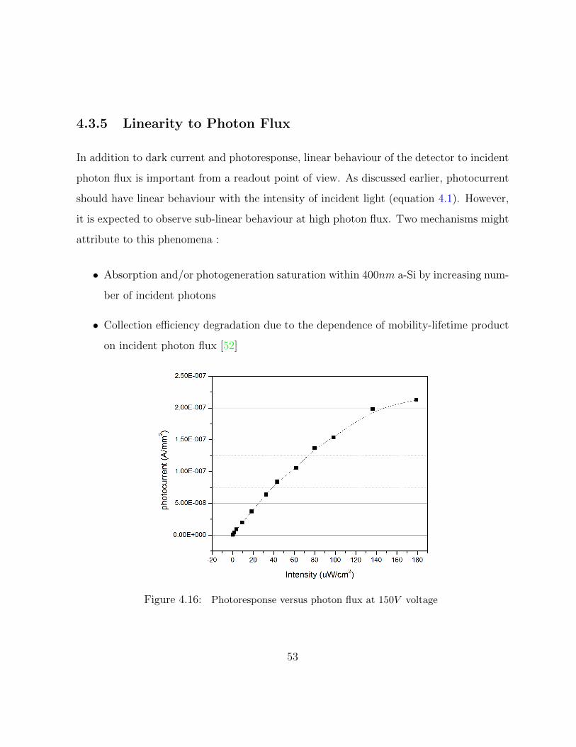
4.3.5 Linearity to Photon Flux
In addition to dark current and photoresponse, linear behaviour of the detector to incident
photon flux is important from a readout point of view. As discussed earlier, photocurrent
should have linear behaviour with the intensity of incident light (equation 4.1). However,
it is expected to observe sub-linear behaviour at high photon flux. Two mechanisms might
attribute to this phenomena :
• Absorption and/or photogeneration saturation within 400nm a-Si by increasing num-
ber of incident photons
• Collection efficiency degradation due to the dependence of mobility-lifetime product
on incident photon flux [52]
Figure 4.16: Photoresponse versus photon flux at 150V voltage
53
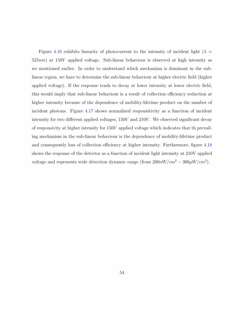
Figure 4.16 exhibits linearity of photocurrent to the intensity of incident light (λ =
525nm) at 150V applied voltage. Sub-linear behaviour is observed at high intensity as
we mentioned earlier. In order to understand which mechanism is dominant in the sub-
linear region, we have to determine the sub-linear behaviour at higher electric field (higher
applied voltage). If the response tends to decay at lower intensity at lower electric field,
this would imply that sub-linear behaviour is a result of collection efficiency reduction at
higher intensity because of the dependence of mobility-lifetime product on the number of
incident photons. Figure 4.17 shows normalized responsitivity as a function of incident
intensity for two different applied voltages, 150V and 210V . We observed significant decay
of responsivity at higher intensity for 150V applied voltage which indicates that th prevail-
ing mechanism in the sub-linear behaviour is the dependence of mobility-lifetime product
and consequently loss of collection efficiency at higher intensity. Furthermore, figure 4.18
shows the response of the detector as a function of incident light intensity at 210V applied
voltage and represents wide detection dynamic range (from 200nW/cm2 − 300µW/cm2).
54
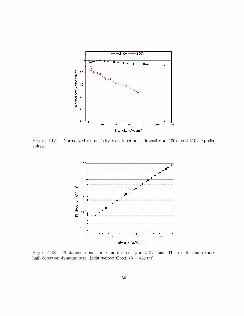
Figure 4.17: Normalized responsivity as a function of intensity at 150V and 210V appliedvoltage
Figure 4.18: Photocurrent as a function of intensity at 210V bias. This result demonstrateshigh detection dynamic rage. Light source: Green (λ = 525nm)
55
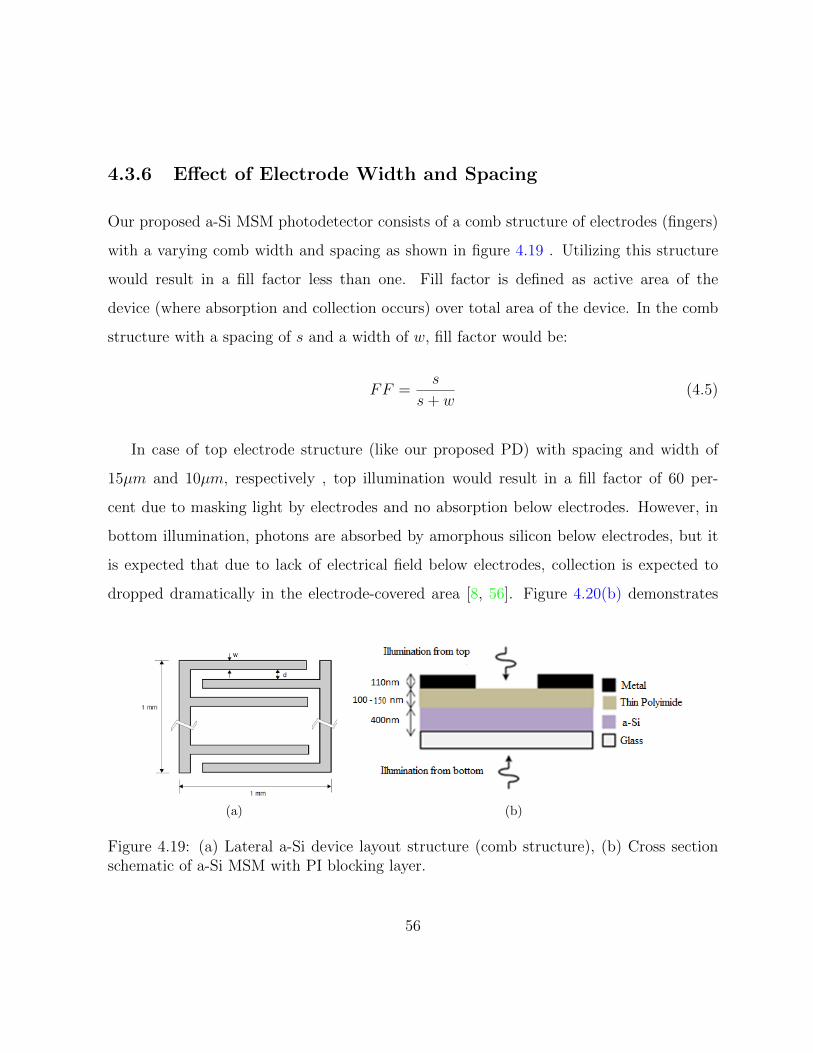
4.3.6 Effect of Electrode Width and Spacing
Our proposed a-Si MSM photodetector consists of a comb structure of electrodes (fingers)
with a varying comb width and spacing as shown in figure 4.19 . Utilizing this structure
would result in a fill factor less than one. Fill factor is defined as active area of the
device (where absorption and collection occurs) over total area of the device. In the comb
structure with a spacing of s and a width of w, fill factor would be:
FF =s
s+ w(4.5)
In case of top electrode structure (like our proposed PD) with spacing and width of
15µm and 10µm, respectively , top illumination would result in a fill factor of 60 per-
cent due to masking light by electrodes and no absorption below electrodes. However, in
bottom illumination, photons are absorbed by amorphous silicon below electrodes, but it
is expected that due to lack of electrical field below electrodes, collection is expected to
dropped dramatically in the electrode-covered area [8, 56]. Figure 4.20(b) demonstrates
(a) (b)
Figure 4.19: (a) Lateral a-Si device layout structure (comb structure), (b) Cross sectionschematic of a-Si MSM with PI blocking layer.
56
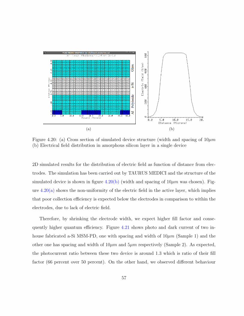
(a) (b)
Figure 4.20: (a) Cross section of simulated device structure (width and spacing of 10µm(b) Electrical field distribution in amorphous silicon layer in a single device
2D simulated results for the distribution of electric field as function of distance from elec-
trodes. The simulation has been carried out by TAURUS MEDICI and the structure of the
simulated device is shown in figure 4.20(b) (width and spacing of 10µm was chosen). Fig-
ure 4.20(a) shows the non-uniformity of the electric field in the active layer, which implies
that poor collection efficiency is expected below the electrodes in comparison to within the
electrodes, due to lack of electric field.
Therefore, by shrinking the electrode width, we expect higher fill factor and conse-
quently higher quantum efficiency. Figure 4.21 shows photo and dark current of two in-
house fabricated a-Si MSM-PD, one with spacing and width of 10µm (Sample 1) and the
other one has spacing and width of 10µm and 5µm respectively (Sample 2). As expected,
the photocurrent ratio between these two device is around 1.3 which is ratio of their fill
factor (66 percent over 50 percent). On the other hand, we observed different behaviour
57
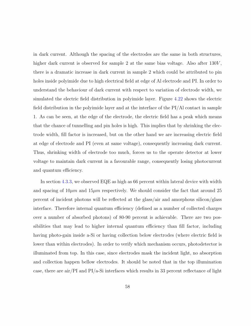
in dark current. Although the spacing of the electrodes are the same in both structures,
higher dark current is observed for sample 2 at the same bias voltage. Also after 130V ,
there is a dramatic increase in dark current in sample 2 which could be attributed to pin
holes inside polyimide due to high electrical field at edge of Al electrode and PI. In order to
understand the behaviour of dark current with respect to variation of electrode width, we
simulated the electric field distribution in polyimide layer. Figure 4.22 shows the electric
field distribution in the polyimide layer and at the interface of the PI/Al contact in sample
1. As can be seen, at the edge of the electrode, the electric field has a peak which means
that the chance of tunnelling and pin holes is high. This implies that by shrinking the elec-
trode width, fill factor is increased, but on the other hand we are increasing electric field
at edge of electrode and PI (even at same voltage), consequently increasing dark current.
Thus, shrinking width of electrode too much, forces us to the operate detector at lower
voltage to maintain dark current in a favourable range, consequently losing photocurrent
and quantum efficiency.
In section 4.3.3, we observed EQE as high as 66 percent within lateral device with width
and spacing of 10µm and 15µm respectively. We should consider the fact that around 25
percent of incident photons will be reflected at the glass/air and amorphous silicon/glass
interface. Therefore internal quantum efficiency (defined as a number of collected charges
over a number of absorbed photons) of 80-90 percent is achievable. There are two pos-
sibilities that may lead to higher internal quantum efficiency than fill factor, including
having photo-gain inside a-Si or having collection below electrodes (where electric field is
lower than within electrodes). In order to verify which mechanism occurs, photodetector is
illuminated from top. In this case, since electrodes mask the incident light, no absorption
and collection happen bellow electrodes. It should be noted that in the top illumination
case, there are air/PI and PI/a-Si interfaces which results in 33 percent reflectance of light
58
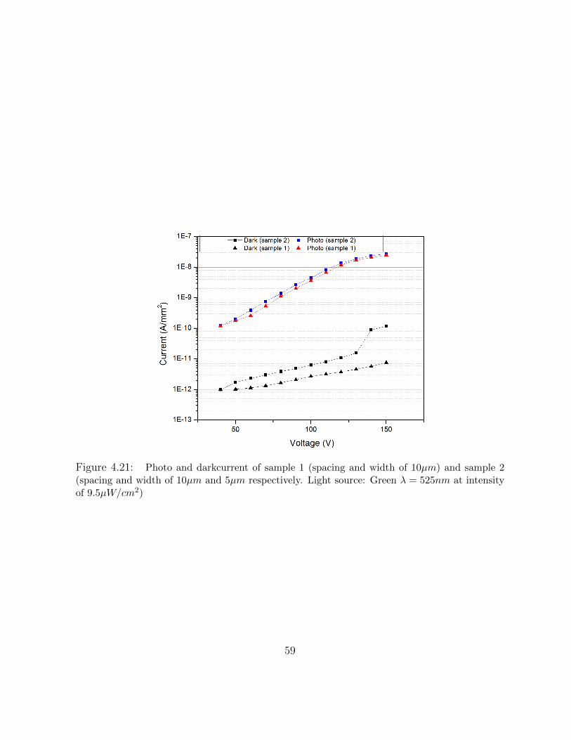
Figure 4.21: Photo and darkcurrent of sample 1 (spacing and width of 10µm) and sample 2(spacing and width of 10µm and 5µm respectively. Light source: Green λ = 525nm at intensityof 9.5µW/cm2)
59
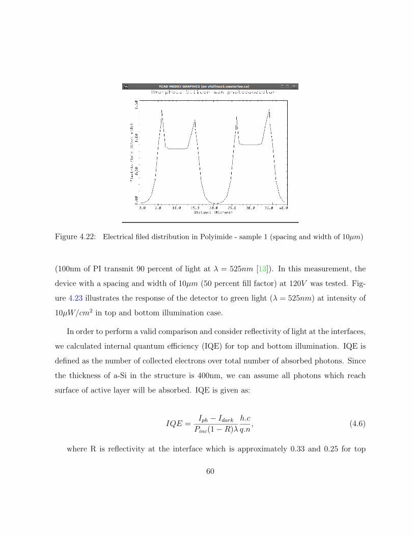
Figure 4.22: Electrical filed distribution in Polyimide - sample 1 (spacing and width of 10µm)
(100nm of PI transmit 90 percent of light at λ = 525nm [13]). In this measurement, the
device with a spacing and width of 10µm (50 percent fill factor) at 120V was tested. Fig-
ure 4.23 illustrates the response of the detector to green light (λ = 525nm) at intensity of
10µW/cm2 in top and bottom illumination case.
In order to perform a valid comparison and consider reflectivity of light at the interfaces,
we calculated internal quantum efficiency (IQE) for top and bottom illumination. IQE is
defined as the number of collected electrons over total number of absorbed photons. Since
the thickness of a-Si in the structure is 400nm, we can assume all photons which reach
surface of active layer will be absorbed. IQE is given as:
IQE =Iph − IdarkPinc(1−R)λ
h.c
q.n, (4.6)
where R is reflectivity at the interface which is approximately 0.33 and 0.25 for top
60
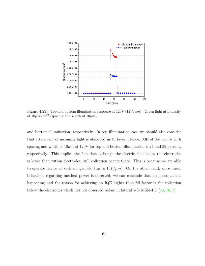
Figure 4.23: Top and bottom illumination response at 120V (12V/µm) - Green light at intensityof 10µW/cm2 (spacing and width of 10µm)
and bottom illumination, respectively. In top illumination case we should also consider
that 10 percent of incoming light is absorbed in PI layer. Hence, IQE of the device with
spacing and width of 10µm at 120V for top and bottom illumination is 24 and 35 percent,
respectively. This implies the fact that although the electric field below the electrodes
is lower than within electrodes, still collection occurs there. This is because we are able
to operate device at such a high field (up to 15V/µm). On the other hand, since linear
behaviour regarding incident power is observed, we can conclude that no photo-gain is
happening and the reason for achieving an IQE higher than fill factor is the collection
below the electrodes which has not observed before in lateral a-Si MSM-PD [56, 16, 8]
61
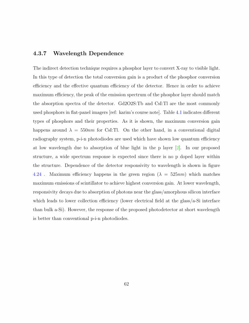
4.3.7 Wavelength Dependence
The indirect detection technique requires a phosphor layer to convert X-ray to visible light.
In this type of detection the total conversion gain is a product of the phosphor conversion
efficiency and the effective quantum efficiency of the detector. Hence in order to achieve
maximum efficiency, the peak of the emission spectrum of the phosphor layer should match
the absorption spectra of the detector. Gd2O2S:Tb and CsI:Tl are the most commonly
used phosphors in flat-panel imagers [ref: karim’s course note]. Table 4.1 indicates different
types of phosphors and their properties. As it is shown, the maximum conversion gain
happens around λ = 550nm for CsI:Tl. On the other hand, in a conventional digital
radiography system, p-i-n photodiodes are used which have shown low quantum efficiency
at low wavelength due to absorption of blue light in the p layer [2]. In our proposed
structure, a wide spectrum response is expected since there is no p doped layer within
the structure. Dependence of the detector responsivity to wavelength is shown in figure
4.24 . Maximum efficiency happens in the green region (λ = 525nm) which matches
maximum emissions of scintillator to achieve highest conversion gain. At lower wavelength,
responsivity decays due to absorption of photons near the glass/amorphous silicon interface
which leads to lower collection efficiency (lower electrical field at the glass/a-Si interface
than bulk a-Si). However, the response of the proposed photodetector at short wavelength
is better than conventional p-i-n photodiodes.
62
Table 4.1: Physical properties of inorganic phosphors
Type Z K-edge energy (keV) Maximum emission Conversion gain
wavelength (nm) Γ (keV −1)
CaWO4 74 69.5 480±100 30Gd2O2S:Tb 64 50.2 550±20 60
CsI:Na 55/53 36/33 415±50 40CsI:Tl 55/53 36/33 560±80 55
Figure 4.24: Responsitivity for three different wavelength. Device: a-Si MSM-PD with thin PIand width and spacing of 10µm. Intensity: 18µW/cm2.
63
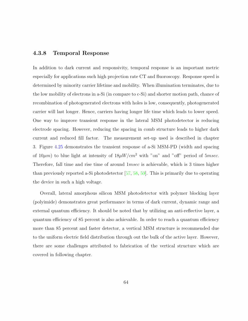
4.3.8 Temporal Response
In addition to dark current and responsivity, temporal response is an important metric
especially for applications such high projection rate CT and fluoroscopy. Response speed is
determined by minority carrier lifetime and mobility. When illumination terminates, due to
the low mobility of electrons in a-Si (in compare to c-Si) and shorter motion path, chance of
recombination of photogenerated electrons with holes is low, consequently, photogenerated
carrier will last longer. Hence, carriers having longer life time which leads to lower speed.
One way to improve transient response in the lateral MSM photodetector is reducing
electrode spacing. However, reducing the spacing in comb structure leads to higher dark
current and reduced fill factor. The measurement set-up used is described in chapter
3. Figure 4.25 demonstrates the transient response of a-Si MSM-PD (width and spacing
of 10µm) to blue light at intensity of 18µW/cm2 with ”on” and ”off” period of 5msec.
Therefore, fall time and rise time of around 1msec is achievable, which is 3 times higher
than previously reported a-Si photodetector [57, 58, 59]. This is primarily due to operating
the device in such a high voltage.
Overall, lateral amorphous silicon MSM photodetector with polymer blocking layer
(polyimide) demonstrates great performance in terms of dark current, dynamic range and
external quantum efficiency. It should be noted that by utilizing an anti-reflective layer, a
quantum efficiency of 85 percent is also achievable. In order to reach a quantum efficiency
more than 85 percent and faster detector, a vertical MSM structure is recommended due
to the uniform electric field distribution through out the bulk of the active layer. However,
there are some challenges attributed to fabrication of the vertical structure which are
covered in following chapter.
64
Figure 4.25: Temporal response of lateral a-Si MSM-PD to pulse light width of 5msec andperiod of 10msec. Device is biased at 120V with width and spacing of 10µm . Light source: Blue- Intensity: 18µW/cm2.
65
Chapter 5
Vertical a-Si MSM Photodetector
Hitherto, we have discussed the performance of a lateral a-Si MSM photodetector and
demonstrated improvements by introducing a thin blocking layer (polyimide) between
amorphous silicon and the metal contacts. Advantages which are attributed to lateral
MSM photodetectors have been named including low cost and simple fabrication process,
compatibility with TFT fabrication process, no top electrode to block incoming photons,
low dark current, high quantum efficiency and etc.. In order to achieve high transient
response (fall and rise time less than 1ms), shrinking electrode spacing in the lateral struc-
ture is one way to be considered. However, shrinking electrode spacing leads to higher
dark current and consequently reduces operating voltage of the detector, losing quantum
efficiency. Therefore, in order to have the ability to operate the detector at high frame
rates and obtain quantum efficiency greater than 85 percent, using vertical structure is
suggested primarily due to uniform electric field through out the bulk of a-Si as well as
shorter spacing between electrodes. However, there are some challenges attributed to the
vertical structure that need more investigation to overcome. In this chapter, first perfor-
66
mance of fabricated vertical MSM photodetector is demonstrated in terms of dark current
and response, followed by challenges which need more investigation to obtain desirable
performance.
5.1 Device Structure
Since the lateral a-Si MSM structures exhibit remarkable performance in dark current and
responsivity by utilizing a blocking layer, the same structure was applied to the vertical
MSM. Figure 5.1 shows vertical structure. Two types of Indium Tin Oxide coated glass
(ITO) have been used as a bottom transparent electrode, including textured and smooth
surface. Textured surface improves responsivity of the detector due to inhibiting photons
from escaping layers. However, it has been understood that a textured substrate increases
dark current. Polyimide on both sides has been spin coated in the same way that it has been
done on the lateral structure. Regarding amorphous silicon, due to limitations on Plasma
Enhanced Chemical Vapour Deposition (PECVD) machine, we weren’t able to deposit the
i-layer with the same machine and recipe that we did for the lateral structure. In the
PECVD machine that was used for lateral structure, the substrate faces down inside the
chamber. In the vertical structure, unlike lateral, for a-Si deposition, ITO glass is coated
with the polyimide layer which is facing down in the chamber of the PECVD machine with
a deposition temperature of 260C, therefore there is a risk of polyimide delaminatingis
high. in courtesy of other lab users and to avoid contamination, I switched to different
machine (Plasmatherm system). Also, Aluminium was used for top electrode.
67
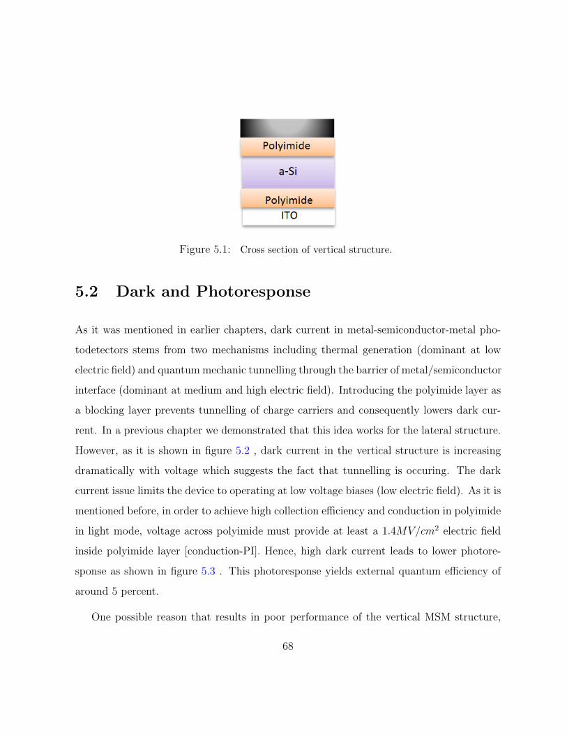
Figure 5.1: Cross section of vertical structure.
5.2 Dark and Photoresponse
As it was mentioned in earlier chapters, dark current in metal-semiconductor-metal pho-
todetectors stems from two mechanisms including thermal generation (dominant at low
electric field) and quantum mechanic tunnelling through the barrier of metal/semiconductor
interface (dominant at medium and high electric field). Introducing the polyimide layer as
a blocking layer prevents tunnelling of charge carriers and consequently lowers dark cur-
rent. In a previous chapter we demonstrated that this idea works for the lateral structure.
However, as it is shown in figure 5.2 , dark current in the vertical structure is increasing
dramatically with voltage which suggests the fact that tunnelling is occuring. The dark
current issue limits the device to operating at low voltage biases (low electric field). As it is
mentioned before, in order to achieve high collection efficiency and conduction in polyimide
in light mode, voltage across polyimide must provide at least a 1.4MV/cm2 electric field
inside polyimide layer [conduction-PI]. Hence, high dark current leads to lower photore-
sponse as shown in figure 5.3 . This photoresponse yields external quantum efficiency of
around 5 percent.
One possible reason that results in poor performance of the vertical MSM structure,
68
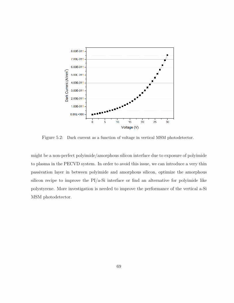
Figure 5.2: Dark current as a function of voltage in vertical MSM photodetector.
might be a non-perfect polyimide/amorphous silicon interface due to exposure of polyimide
to plasma in the PECVD system. In order to avoid this issue, we can introduce a very thin
passivation layer in between polyimide and amorphous silicon, optimize the amorphous
silicon recipe to improve the PI/a-Si interface or find an alternative for polyimide like
polystyrene. More investigation is needed to improve the performance of the vertical a-Si
MSM photodetector.
69
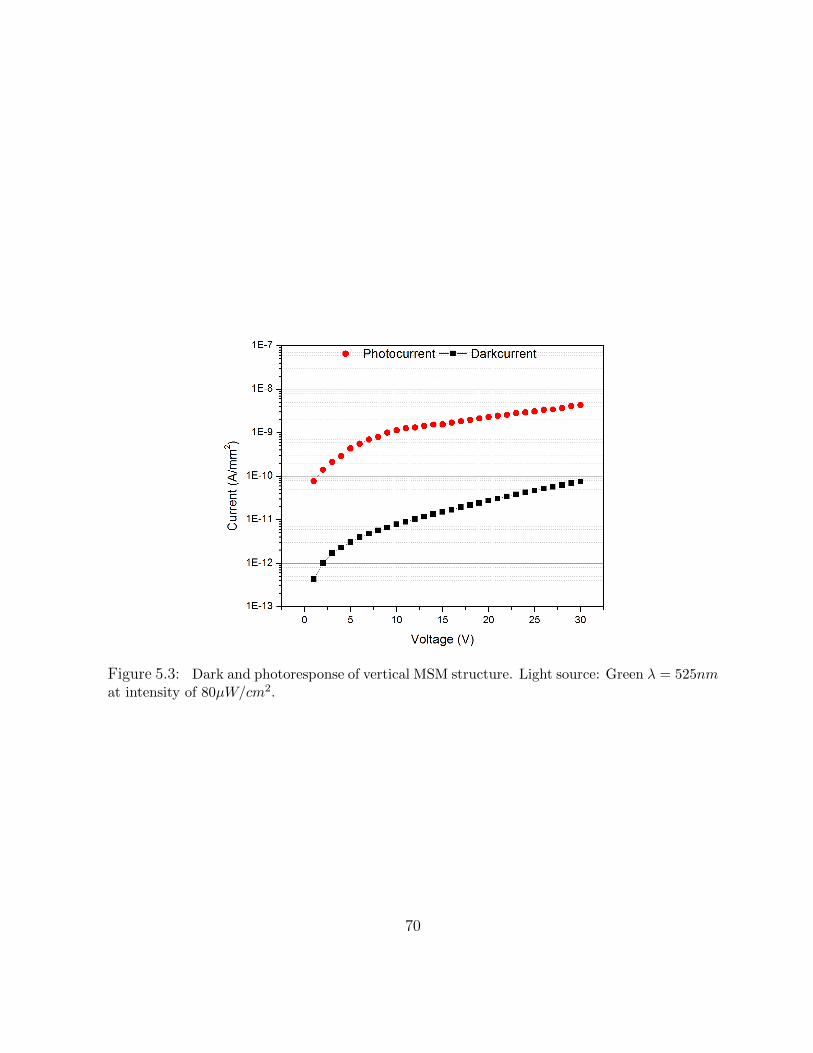
Figure 5.3: Dark and photoresponse of vertical MSM structure. Light source: Green λ = 525nmat intensity of 80µW/cm2.
70
Chapter 6
Conclusion
The most promising technology for radiography is active matrix flat panel imaging sys-
tems (AMFPI). However, AMFPI systems are relatively expensive in comparison with
conventional computed radiography (CR) systems. Therefore for general radiography ap-
plications low cost systems are needed, especially in hospitals and healthcare systems of
the developing countries. The focus of this research is the fabrication and characterization
of a low cost amorphous silicon metal-semiconductor-metal photodetector as a photosen-
sitive element in a AMFPI systems. Here the criteria considered for the MSM-PD are
performance quality and potential to be manufacturable as a low cost digital radiography
system. AMFPI technology is the same as a-Si:H TFT manufacturing technology used to
make display. Photosensitive element in AMFPI is a part that increases the cost of the flat
panel imager. Currently most of AMFPIs benefit from the p-i-n photodiodes. However,
due to the necessity of doped p+ layer, fabrication of photodiode cannot be performed
with the same process as a-Si:H TFT. In this work a new lateral a-Si MSM-PD structure
is proposed as a replacement for p-i-n photodiode which is commercially used in flat panel
71
imager.
Metal-Semiconductor-Metal photodetectors (MSM-PD) are attractive as sensors due
to their ease of fabrication and compatibility with thin film transistor fabrication process
primarily because there is no p+ doped layer in comparison with conventional p-i-n pho-
todiodes. Previously reported a-Si MSM-PDs exhibited high dark current, instability of
dark current and lower EQE in compared to the conventional p-i-n photodiodes. The main
challenge in this research was finding an approach to minimize and stabilize dark current
without any significant deterioration in its performance through systematic studies on pho-
toresponse of the detector. We have demonstrated low dark current a-Si MSM-PD (lower
than 20pA/mm2) with responsivity of 280mA/W and EQE of 65 percent to green light
(λ = 525nm). These improvement are achieved by introduction of a PI blocking layer and
operating the device at high electric field (15V/µm). This new structure eliminates the
need of p+ and n+ layers which makes this structure fully compatible with the a-Si:H TFT
fabrication process and consequently a low cost flat panel imager.
Dark current in the a-Si MSM-PD origins from thermal generation and quantum me-
chanical tunnelling (thermionic emission) of carriers through the metal/a-Si barrier. In-
stability of dark current in previously reported a-Si MSM-PDs stems from the variation
of the barrier width at the metal/a-Si interface overtime. This leads to variation of tun-
nelling rate and consequently instability of dark current. Introducing PI blocking layer
reduces the tunnelling rate and maintain dark current in the range of the thermal gener-
ation of a-Si. Hence, variation of the barrier width at the metal/a-Si interface does not
affect dark current in a-Si MSM-PD with PI blocking layer. In addition to dark current
and responsivity, we have studied the behaviour of the detector to the flux of the incident
photons. Linear behaviour is expected in all range of the photon flux. However, at high
intensity sub-linear behaviour is observed. We demonstrated that since the detector main-
72
tains its linear behaviour better at higher electric field (15V/µm) than lower electric field
(10V/µm), the mechanism that attributed to the sub-linear behaviour at high intensity
is the dependence of the mobility life-time product to the number of incoming photons.
Moreover, we presented a wide detection dynamic range from 200nW/cm2 − 300µW/cm2
with linear responsivity.
Further, in order to find the best configuration of the lateral structure, we have stud-
ied the effect of the spacing and width of the comb structure. Based on the electric field
simulation in the lateral structure and the non-uniform electric field distribution, although
absorption occurs below the electrodes (bottom illumination case), lower collection effi-
ciency is expected there. Hence, higher fill factor is favourable to have higher quantum
efficiency. However, due to the shape of the electric field distribution in PI layer at the
edge of the Al/PI interface, shrinking the width of the electrode will result in higher dark
current (even at the same voltage and spacing) and consequently confines the detector to
operated at lower bias voltage which results in lower EQE. Based on experimental results,
lateral structure with spacing and width of 15µm and 10µm (fill factor of 60 percent)
demonstrated the best performance at 210 V bias voltage. Moreover, for the first time
we experimentally showed that although the electric field below the electrodes is lower
than within the electrodes in bulk of the a-Si, collection occurs below the electrodes (but
with lower efficiency). This implies that even with fill factor of 60 percent, EQE more
than 60 is achievable. We also present the response spectrum of the detector which shows
wider spectrum than p-i-n photodiodes especially in lower wavelength (blue region) due to
eliminating p+ layer. Finally, we demonstrated rise and fall time of 1msec which is three
times lower than previously reported a-Si MSM-PD which can be attributed to operating
the detector at high electrical filed and having higher collection efficiency.
73
References
[1] F. H. Attix. Introduction to Radiological Physics and Radiation Dosimetry. John
Wiley, New York, 1986.
[2] R. A. Street. Hydrogenated Amorphus Silicon. Cambridge University, London, 1991.
[3] Mohammad Hadi Izadi. Multi-mode Pixel Architectures for Large Area Real-Time
X-ray Imaging. PhD thesis, University of Waterloo, 2010.
[4] Siebert JA. Digital radiography: the bottom line comparison of cr and dr technology.
Appl Radiol, 2009.
[5] Michael Musashi Adachi. Development and characterization of PECVD grown silicon
nanowires for thin film photovoltaics. PhD thesis, University of Waterloo, 2012.
[6] Koorosh Aflatooni. X-Ray Detection Using Amorphous Silicon Technology. PhD
thesis, University of Waterloo, 1998.
[7] H. Scher and E. W. Montroll. Anomalous transit-the dispertion in amorphous solids.
Phys. Rev. B, 1975.
74
[8] F. Taghibakhsh, I. Khodami, and K. S. Karim. Characterization of short-wavelength-
selective a-si:h msm photoconductors for large-area digital-imaging applications. IEEE
Trans Electron Devices, 2008.
[9] K. Aflatooni, R. Homsey, and A. Nathan. Reverse current instabilities in amorphous
silicon schottky diodes: Modeling and experiments. IEEE Trans. Electron Devices,
1999.
[10] Kevles and Bettyann Holtzmann. Naked to the Bone Medical Imaging in the Twentieth
Century. Camden, NJ, 1996.
[11] Sample Sharro. The electromagnetic spectrum., x-rays. Technical report, NASA,
2007.
[12] W.R. Hendee and E.R. Ritenour. Medical Imaging Physics. Wiley-Liss, NY, 2002.
[13] S. Abbaszadeh, N. Allec, S. Ghanbarzadeh, U. Shafique, and K. S. Karim. Investiga-
tion of hole-blocking contact for high conversion gain amorphous selenium detectors
for x-ray imaging. IEEE Trans Electron Devices, 2012.
[14] M.J. Yaffe and J.A. Rowlands. X-ray detectors for digital radiology. Physics in
Medicine and Biology, 1997.
[15] M. Bath, P. Sund, and L.G. Mansson. Evaluation of the imaging properties of two
generations of a ccd-based system for digital chest radiography. Medical Physics, 2002.
[16] F. Taghibakhsh and K. S. Karim. Fabrication and characterization of nickel amor-
phous silicon metalsemiconductormetal photoconductors. Proc. 20th Can. Conf. Elect.
Comput. Eng., 2007.
75
[17] C. Kittel. Introduction to Solid State Physics. John Wiley and Sons, New York, 1986.
[18] A. Madan and M.P. Shaw. The Physics and Applications of Amorphous Semiconduc-
tors. Academic Press, 1988.
[19] Z. E.Smith and S. Wagner. Implications of the defect pool concept for metastable and
stable defects in amorphous silicon. Amorphous Silicon and Related Materials. World
Scientific, 1989.
[20] D.L. Staebler and C.R. Wronski. Reversible conductivity changes in dischargepro-
duced amorphous si. Appl. Phys. Lett, 1977.
[21] A. Shah, P. Torres, R. Tscharner, N. Wyrsch, and H. Keppner. Photovoltaic technol-
ogy: The case for thin-film solar cells. Science, 1999.
[22] J. Meier, R. Fluckiger, H. Keppner, and A. Shah. Complete microcrystalline p-i-n
solar cell crystalline or amorphous cell behavior? Appl. Phys. Lett, 1994.
[23] D. L. Rogers. Integrated optical receivers using msm detectors. J. Lightwave Technol.,
1991.
[24] S. M. SZE, D. J. COLEMAN, and A. LOYA. Current transport in metal-
semiconductor-metal (msm) structures. Solid-Stare EIecfronics, 1971.
[25] C. W. Slayman and L. Figueroa. Frequency and pulse response of a novel high speed
interdigital surface photoconductor (idpc). IEEE Electron Dev. Lett., 1981.
[26] L. Figueroa and C. W. Slayman. A novel heterostructure interdigital photodetector
(hip) with picosecond optical response. IEEE Electron Dev. Lett., 1981.
76
[27] C. J. Wei, H. J. Klein, and H. Beneking. Symmetrical mott barrier as a fast photode-
tector. Electron Lett, 1981.
[28] U. Schade, S. Kollakowski, E. H. Bottcher, and D. Bimberg. Improved performance
of large-area inp/ingaas metal-semiconductor-metal photodetectors by sulfured passi-
vation. Appl. Phys. Lett, 1994.
[29] S. D. Kwon, C. H. Kim, H. K. Kwon, B. D. Choe, and H. J. Lim. Interface properties
of (nh4)2sx-treated in0.5ga0.5p schottky contacts. J. Appl. Phys., 1995.
[30] C. R. Moon, B. D. Choe, S. D. Kwon, and H. Lim. Difference of interface trap
passivation in schottky contacts formed on (nh4)2sx-treated gaas and in0.5ga0.5p. J.
Appl. Phys., 1997.
[31] W. C. Koscielniak, R. M. Kolbas, , and M. A. Littlejohn. Photocurrent enhancement
in a gaas metal-semiconductor-metal photodetector due to ultrasmall au islands. Appl.
Phys. Lett., 1988.
[32] P. Ambree and K. Wandel. Plasma enhanced chemical vapor deposited sio2 layers for
passivation of ingaas:fe metal-semiconductor-metal photodetectors. J. Appl. Phys.,
1995.
[33] S. Kollakowski, U. Schade, E. H. Bottcher, D. Bimberg D. Kuhl, P. Ambree, and
K. Wandel. Silicon dioxide passivation of inp/ingaas metal-semiconductormetal pho-
todetectors. J. Vac. Sci. Technol., 1996.
[34] M. A. Martin and J. G. Simmons. Polyimide passivated semitransparent
in0.49ga0.51p/gaas msm photodetector operating at 840 nm wavelength. Microwave
and Optical Technol. Lett., 1999.
77
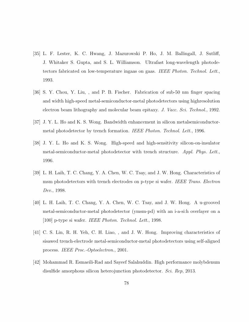
[35] L. F. Lester, K. C. Hwang, J. Mazurowski P. Ho, J. M. Ballingall, J. Sutliff,
J. Whitaker S. Gupta, and S. L. Williamson. Ultrafast long-wavelength photode-
tectors fabricated on low-temperature ingaas on gaas. IEEE Photon. Technol. Lett.,
1993.
[36] S. Y. Chou, Y. Liu, , and P. B. Fischer. Fabrication of sub-50 nm finger spacing
and width high-speed metal-semiconductor-metal photodetectors using highresolution
electron beam lithography and molecular beam epitaxy. J. Vacc. Sci. Technol., 1992.
[37] J. Y. L. Ho and K. S. Wong. Bandwidth enhancement in silicon metalsemiconductor-
metal photodetector by trench formation. IEEE Photon. Technol. Lett., 1996.
[38] J. Y. L. Ho and K. S. Wong. High-speed and high-sensitivity silicon-on-insulator
metal-semiconductor-metal photodetector with trench structure. Appl. Phys. Lett.,
1996.
[39] L. H. Laih, T. C. Chang, Y. A. Chen, W. C. Tsay, and J. W. Hong. Characteristics of
msm photodetectors with trench electrodes on p-type si wafer. IEEE Trans. Electron
Dev., 1998.
[40] L. H. Laih, T. C. Chang, Y. A. Chen, W. C. Tsay, and J. W. Hong. A u-grooved
metal-semiconductor-metal photodetector (ymsm-pd) with an i-a-si:h overlayer on a
[100] p-type si wafer. IEEE Photon. Technol. Lett., 1998.
[41] C. S. Lin, R. H. Yeh, C. H. Liao, , and J. W. Hong. Improving characteristics of
sisawed trench-electrode metal-semiconductor-metal photodetectors using self-aligned
process. IEEE Proc.-Optoelectron., 2001.
[42] Mohammad R. Esmaeili-Rad and Sayeef Salahuddin. High performance molybdenum
disulfide amorphous silicon heterojunction photodetector. Sci. Rep, 2013.
78
[43] N. Kramer and C. V. Berkel. Reverse current mechanisms in amorphous silicon diodes.
Appl. Phys. Lett, 1994.
[44] R A. Street. Long-time transient conduction in a-si:h p-i-n devices. Phil. Mag. B,
1991.
[45] J. K. Aron and S. J. Fonash. Origins of reverse bias leakage current in hydrogenated
amorphous silicon p-i-n detector structures. Appl. Phys. Lett., 1992.
[46] J. K. Aron and S. J. Fonash. Using reverse bias currents to differentiate between
bulk degradation and interfacial degradation in hydrogenated amorphous silicon p-i-n
structures. J. Appl. Phys., 1992.
[47] R. Homsey, K. Aflatooni, and A. Nathan. Reverse current transient behaviour in
amorphous silicon schottky diodes at low biases. Appl. Phys. lett., 1997.
[48] T. Tiedje and A. Rose. A physical interpretation of dispresive transport in disordered
semiconductors. Solid state communications, 1980.
[49] C. R. Wronski and D. E. Carison. Surface states and barrier heights of metal-
amorphous silicon schottky barriers. Solid State Comm., 1977.
[50] Anthony W. Sarto and Bart J. Van Zeghbroeck. Photocurrents in a metalsemiconduc-
tormetal photodetector. IEEE JOURNAL OF QUANTUM ELECTRONICS, 1997.
[51] J. I. Ruy, S. H. Won, J. H. Hur, H. J. Kim, and J. Jang. Simulation of a novel
amorphous silicon photoconductor array. J. Korean Phys. Soc., 2001.
[52] R. E. Stearns and R. L. Weisfield. Two dimensional amorphous-silicon photoconductor
array for optical imaging. J. Appl. Opt., 1992.
79
[53] Masanori Ito and Osamu Wada. Low dark current gaas metal-semiconductor-
metal(msm) photodiodes using wsix contacts. IEEE JOURNAL OF QUANTUM
ELECTRONICS, 1986.
[54] Yu Chin Lim and Robert A. Moore. Properties of alternately charged coplanar parallel
strips by conformal mappings. IEEE TRANSACTIONS ON ELECTRON DEVICES,,
1968.
[55] N. R. Tu and K. C. Kao. High-field electrical conduction in polyimide films. J. Appl.
Phys, 1999.
[56] S. Abbaszadeh, N. Allec, and K.S. Karim. Characterization of low dark-current lat-
eral amorphous-selenium metal-semiconductor-metal photodetectors. Sensors Jour-
nal, IEEE, 2013.
[57] J. H Siewerdsen and D. A. Jaffray. A ghost story: Spatio-temporal response charac-
teristics of an indirect-detection flat-panel imager. Med. Phys., 1999.
[58] S. Takayama, K. Mori, K. Suzuki, and C. Tanuma. An a-si:h photoconductive sensor
with a gate electrode. IEEE Trans. Electron Devices, 1993.
[59] J. A Seibert. Flat-panel detectors: how much better are they? Pediatr Radiol, 2006.
80