high performance multi-channel audio codec · pdf file20 tst3 21 tst4 22 33 32 31 30 29 28 27...
TRANSCRIPT

[AK4626A]
MS0397-E-01 2012/09 - 1 -
GENERAL DESCRIPTION The AK4626A is a single chip CODEC that includes two channels of ADC and six channels of DAC. The ADC outputs 24bit data and the DAC accepts up to 24bit input data. The ADC has the Enhanced Dual Bit architecture with wide dynamic range. The DAC introduces the newly developed Advanced Multi-Bit architecture, and achieves wider dynamic range and lower outband noise. An auxiliary digital audio input interface maybe used instead of the ADC for passing audio data to the primary audio output port. Control may be set directly by pins or programmed through a separate serial interface. The AK4626A has a dynamic range of 102dB for ADC, 106dB for DAC and is well suited for digital surround for home theater and car audio. An AC-3 system can be built with a IEC60958(SPDIF) receiver such as the AK4112B. The AK4626A is available in a small 44pin LQFP package which will reduce system space. *AC-3 is a trademark of Dolby Laboratories.
FEATURES 2ch 24bit ADC
- 64x Oversampling - Sampling Rate up to 96kHz - Linear Phase Digital Anti-Alias Filter - Single-Ended Input - S/(N+D): 92dB - Dynamic Range, S/N: 102dB - Digital HPF for offset cancellation - I/F format: MSB justified, I2S or TDM - Overflow flag
6ch 24bit DAC - 128x Oversampling - Sampling Rate up to 192kHz - 24bit 8 times Digital Filter - Single-Ended Outputs - On-chip Switched-Capacitor Filter - S/(N+D): 90dB - Dynamic Range, S/N: 106dB - I/F format: MSB justified, LSB justified(20bit,24bit), I2S or TDM - Individual channel digital volume with 128 levels and 0.5dB step - Soft mute - De-emphasis for 32kHz, 44.1kHz and 48kHz - Zero Detect Function
High Jitter Tolerance TTL Level Digital I/F 3-wire Serial and I2C Bus µP I/F for mode setting Master clock: 256fs, 384fs or 512fs for fs=32kHz to 48kHz
128fs, 192fs or 256fs for fs=64kHz to 96kHz 128fs for fs=120kHz to 192kHz
Power Supply: 4.5 to 5.5V Power Supply for output buffer: 2.7 to 5.5V Small 44pin LQFP AK4626 Pin Compatible
High Performance Multi-channel Audio CODECAK4626A

[AK4626A]
MS0397-E-01 2012/09 - 2 -
Block Diagram
AudioI/F
LPF
LPF DAC DATT
LPF DAC DATT
LPF DAC DATT
LPF DAC DATT
LPF DAC DATT
LOUT1
ROUT1
LOUT2
ROUT2
LOUT3
ROUT3
DAC DATT
AK4626A
ADC HPF
ADC HPF RIN
LIN
LRCK BICK
SDOUT1 SDOUT2 SDOUT3
AC3
SDIN
MCKO LRCK BICK
XTI
XTO DIR
SDTO
AK4112B
RX4RX3 RX2 RX1
LRCKBICK
SDTI1SDTI2SDTI3
DAUX
SDOS
MCLK
LRCKBICK
SDOUT
SDIN1SDIN2SDIN3
MCLK
SDTO
Format Converter
Block Diagram (DIR and AC-3 DSP are external parts)
[AK4626A]
MS0397-E-01 2012/09 - 3 -
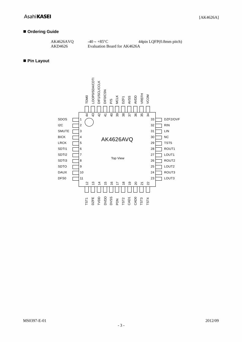
Ordering Guide AK4626AVQ -40 ∼ +85°C 44pin LQFP(0.8mm pitch)
AKD4626 Evaluation Board for AK4626A
Pin Layout
SDOS
TDM
0
1
I2C
44
2
SMUTE 3
BICK 4
LRCK 5
SDTI1 6
SDTI2 7
SDTI3 8
SDTO 9
DAUX 10
DFS0 11
LOO
P0/
SD
A/C
DTI
43
DIF
1/S
CL/
CC
LK
42 41 40
MC
LK
39
DZF
1 38
AVS
S
37
AVD
D
36
VR
EFH
35
VC
OM
34
TST1
12
DZF
E
13
TVD
D
14
DV
DD
15
DV
SS
16
17
TST2
18
CA
D1
19
CA
D0
20
TST3
21
TST4
22
33
32
31
30
29
28
27
26
25
24
23
DZF2/OVF
RIN
LIN
NC
TST5
ROUT1
LOUT1
ROUT2
LOUT2
ROUT3
LOUT3
AK4626AVQ
Top View
PD
N
DIF
0/C
SN
P/S

[AK4626A]
MS0397-E-01 2012/09 - 4 -
Compatibility with AK4527B 1. Functions
Functions AK4527B AK4626A DAC Sampling frequency Up to 96kHz Up to 192kHz TDM128 (96kHz) Not available Available Digital Attenuator 256 levels 128 levels Soft Mute Soft mute function is independent of
Digital attenuator. Soft mute function is not independent of Digital attenuator.
Analog Input (ADC) Differential input Single-ended Input 2. Pin Configuration
pin# AK4527B AK4626A 11 DFS DFS0 12 NC TST1 18 TEST TST2 19 NC CAD1 20 ADIF CAD0 21 CAD1 TST3 22 CAD0 TST4 29 LIN- TST5 30 LIN+ NC 31 RIN- LIN 32 RIN+ RIN 44 LOOP1 TDM0
3. Register
Addr AK4527B AK4626A 00H Not available TDM0 00H Not available TDM1 01H DFS DFS0 01H Not available DFS1 09H Not available ATS1, ATS0 0AH Not available DZFM3

[AK4626A]
MS0397-E-01 2012/09 - 5 -
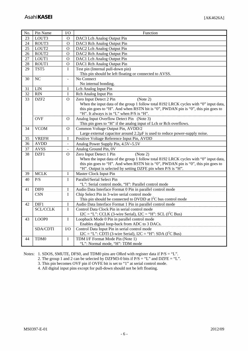
PIN/FUNCTION No. Pin Name I/O Function 1 SDOS I SDTO Source Select Pin (Note 1)
“L”: Internal ADC output, “H”: DAUX input SDOS pin should be set to “L” when TDM= “1”.
2 I2C I Control Mode Select Pin “L”: 3-wire Serial, “H”: I2C Bus
3 SMUTE I Soft Mute Pin (Note 1) When this pin goes to “H”, soft mute cycle is initialized. When returning to “L”, the output mute releases.
4 BICK I Audio Serial Data Clock Pin 5 LRCK I Input Channel Clock Pin 6 SDTI1 I DAC1 Audio Serial Data Input Pin 7 SDTI2 I DAC2 Audio Serial Data Input Pin 8 SDTI3 I DAC3 Audio Serial Data Input Pin 9 SDTO O Audio Serial Data Output Pin
10 DAUX I AUX Audio Serial Data Input Pin 11 DFS0 I Double Speed Sampling Mode Pin (Note 1)
“L”: Normal Speed, “H”: Double Speed 12 TST1 I Test Pin
This pin should be connected to DVSS. 13 DZFE I Zero Input Detect Enable Pin
“L”: mode 7 (disable) at parallel mode, zero detect mode is selectable by DZFM3-0 bits at serial mode
“H”: mode 0 (DZF1 is AND of all six channels) 14 TVDD - Output Buffer Power Supply Pin, 2.7V∼5.5V 15 DVDD - Digital Power Supply Pin, 4.5V∼5.5V 16 DVSS - Digital Ground Pin, 0V 17 PDN I Power-Down & Reset Pin
When “L”, the AK4626A is powered-down and the control registers are reset to default state. If the state of P/S or CAD1-0 changes, then the AK4626A must be reset by PDN.
18 TST2 I Test Pin This pin should be connected to DVSS.
19 CAD1 I Chip Address 1 Pin 20 CAD0 I Chip Address 0 Pin 21 TST3 O Test Pin
This pin should be left floating. 22 TST4 O Test Pin
This pin should be left floating.
[AK4626A]
MS0397-E-01 2012/09 - 6 -
No. Pin Name I/O Function 23 LOUT3 O DAC3 Lch Analog Output Pin 24 ROUT3 O DAC3 Rch Analog Output Pin 25 LOUT2 O DAC2 Lch Analog Output Pin 26 ROUT2 O DAC2 Rch Analog Output Pin 27 LOUT1 O DAC1 Lch Analog Output Pin 28 ROUT1 O DAC1 Rch Analog Output Pin 29 TST5 I Test pin (Internal pull-down pin)
This pin should be left floating or connected to AVSS. 30 NC - No Connect
No internal bonding. 31 LIN I Lch Analog Input Pin 32 RIN I Rch Analog Input Pin
DZF2 O Zero Input Detect 2 Pin (Note 2) When the input data of the group 1 follow total 8192 LRCK cycles with “0” input data, this pin goes to “H”. And when RSTN bit is “0”, PWDAN pin is “0”, this pin goes to “H”. It always is in “L” when P/S is “H”.
33
OVF O Analog Input Overflow Detect Pin (Note 3) This pin goes to “H” if the analog input of Lch or Rch overflows.
34 VCOM O Common Voltage Output Pin, AVDD/2 Large external capacitor around 2.2µF is used to reduce power-supply noise.
35 VREFH I Positive Voltage Reference Input Pin, AVDD 36 AVDD - Analog Power Supply Pin, 4.5V∼5.5V 37 AVSS - Analog Ground Pin, 0V 38 DZF1 O Zero Input Detect 1 Pin (Note 2)
When the input data of the group 1 follow total 8192 LRCK cycles with “0” input data, this pin goes to “H”. And when RSTN bit is “0”, PWDAN pin is “0”, this pin goes to “H”. Output is selected by setting DZFE pin when P/S is “H”.
39 MCLK I Master Clock Input Pin 40 P/S I Parallel/Serial Select Pin
“L”: Serial control mode, “H”: Parallel control mode DIF0 I Audio Data Interface Format 0 Pin in parallel control mode 41 CSN I Chip Select Pin in 3-wire serial control mode
This pin should be connected to DVDD at I2C bus control mode DIF1 I Audio Data Interface Format 1 Pin in parallel control mode 42 SCL/CCLK I Control Data Clock Pin in serial control mode
I2C = “L”: CCLK (3-wire Serial), I2C = “H”: SCL (I2C Bus) LOOP0 I Loopback Mode 0 Pin in parallel control mode
Enables digital loop-back from ADC to 3 DACs. 43
SDA/CDTI I/O Control Data Input Pin in serial control mode I2C = “L”: CDTI (3-wire Serial), I2C = “H”: SDA (I2C Bus)
44 TDM0 I TDM I/F Format Mode Pin (Note 1) “L”: Normal mode, “H”: TDM mode
Notes: 1. SDOS, SMUTE, DFS0, and TDM0 pins are ORed with register data if P/S = “L”.
2. The group 1 and 2 can be selected by DZFM3-0 bits if P/S = “L” and DZFE = “L”. 3. This pin becomes OVF pin if OVFE bit is set to “1” at serial control mode. 4. All digital input pins except for pull-down should not be left floating.

[AK4626A]
MS0397-E-01 2012/09 - 7 -
ABSOLUTE MAXIMUM RATINGS (AVSS=DVSS=0V; Note 5) Parameter Symbol min max Unit Power Supplies Analog
Digital Output buffer |AVSS-DVSS| (Note 6)
AVDD DVDD TVDD ΔGND
-0.3 -0.3 -0.3
-
6.0 6.0 6.0 0.3
V V V V
Input Current (any pins except for supplies) IIN - ±10 mA Analog Input Voltage VINA -0.3 AVDD+0.3 V Digital Input Voltage
(Expect LRCK, BICK pins) (LRCK, BICK pins)
VIND1 VIND2
-0.3 -0.3
DVDD+0.3 TVDD+0.3
V V
Ambient Temperature (power applied) Ta -40 85 °C Storage Temperature Tstg -65 150 °C Notes: 5. All voltages with respect to ground.
6. AVSS and DVSS must be connected to the same analog ground plane. WARNING: Operation at or beyond these limits may result in permanent damage to the device. Normal operation is not guaranteed at these extremes.
RECOMMENDED OPERATING CONDITIONS (AVSS=DVSS=0V; Note 5) Parameter Symbol min typ max Unit Power Supplies
(Note 7) Analog Digital Output buffer
AVDD DVDD TVDD
4.5 4.5 2.7
5.0 5.0 5.0
5.5 5.5 5.5
V V V
Notes: 5. All voltages with respect to ground.
7. The power up sequence between AVDD, DVDD and TVDD is not critical. Do not turn off only the AK4626A under the condition that a surrounding device is powered on and the I2C bus is in use.
WARNING: AKM assumes no responsibility for the usage beyond the conditions in this datasheet.

[AK4626A]
MS0397-E-01 2012/09 - 8 -
ANALOG CHARACTERISTICS (Ta=25°C; AVDD=DVDD=TVDD=5V; AVSS=DVSS=0V; VREFH=AVDD; fs=48kHz; BICK=64fs; Signal Frequency=1kHz; 24bit Data; Measurement Frequency=20Hz∼20kHz at 48kHz, 20Hz~40kHz at fs=96kHz,
20Hz~40kHz at fs=192kHz; unless otherwise specified) Parameter min typ max Unit ADC Analog Input Characteristics Resolution 24 Bits S/(N+D) (-0.5dBFS) fs=48kHz
fs=96kHz 84 -
92 86
dB dB
DR (-60dBFS) fs=48kHz, A-weighted fs=96kHz fs=96kHz, A-weighted
94 88 93
102 96 102
dB dB dB
S/N (Note 8) fs=48kHz, A-weighted fs=96kHz fs=96kHz, A-weighted
94 88 93
102 96 102
dB dB dB
Interchannel Isolation 90 110 dB DC Accuracy Interchannel Gain Mismatch 0.2 0.3 dB Gain Drift 20 - ppm/°CInput Voltage AIN=0.62xVREFH 2.90 3.10 3.30 Vpp Input Resistance (Note 9) 15 25 kΩ Power Supply Rejection (Note 10) 50 dB DAC Analog Output Characteristics Resolution 24 Bits S/(N+D) fs=48kHz
fs=96kHz fs=192kHz
80 78 -
90 88 88
dB dB dB
DR (-60dBFS) fs=48kHz, A-weighted fs=96kHz fs=96kHz, A-weighted fs=192kHz fs=192kHz, A-weighted
95 88 94 - -
106 100 106 100 106
dB dB dB dB dB
S/N (Note 11) fs=48kHz, A-weighted fs=96kHz fs=96kHz, A-weighted fs=192kHz fs=192kHz, A-weighted
95 88 94 - -
106 100 106 100 106
dB dB dB dB dB
Interchannel Isolation 90 110 dB DC Accuracy Interchannel Gain Mismatch 0.2 0.5 dB Gain Drift 20 - ppm/°COutput Voltage AOUT=0.6xVREFH 2.75 3.0 3.25 Vpp Load Resistance 5 kΩ Power Supply Rejection (Note 10) 50 dB Notes: 8. S/N measured by CCIR-ARM is 98dB(@fs=48kHz).
9. Input resistance is 16kΩ typically at fs=96kHz. 10. PSR is applied to AVDD, DVDD and TVDD with 1kHz, 50mVpp. VREFH pin is held a constant voltage. 11. S/N measured by CCIR-ARM is 102dB(@fs=48kHz).

[AK4626A]
MS0397-E-01 2012/09 - 9 -
Parameter min typ max Unit Power Supplies Power Supply Current (AVDD+DVDD+TVDD)
Normal Operation (PDN = “H”) AVDD fs=48kHz,96kHz
fs=192kHz DVDD+TVDD fs=48kHz (Note 12)
fs=96kHz fs=192kHz
Power-down mode (PDN = “L”) TST=”L” (Note 13)
45 34 18 24 27 80
67 51 27 36 40 200
mA mA mA mA mA µA
Notes: 12. TVDD=0.1mA(typ).
13. In the power-down mode. All digital input pins including clock pins (MCLK, BICK, LRCK) are held DVSS.

[AK4626A]
MS0397-E-01 2012/09 - 10 -
FILTER CHARACTERISTICS (Ta=25°C; AVDD=DVDD=4.5∼5.5V; TVDD=2.7∼5.5V; fs=48kHz) Parameter Symbol min typ max Unit ADC Digital Filter (Decimation LPF): Passband (Note 14) ±0.1dB
-0.2dB -3.0dB
PB 0 - -
20.0 23.0
18.9 - -
kHz kHz kHz
Stopband SB 28 kHz Passband Ripple PR ±0.04 dB Stopband Attenuation SA 68 dB Group Delay (Note 15) GD 16 1/fs Group Delay Distortion ΔGD 0 µs ADC Digital Filter (HPF): Frequency Response (Note 14) -3dB
-0.1dB FR 1.0
6.5 Hz
Hz DAC Digital Filter: Passband (Note 14) -0.1dB
-6.0dB PB 0
-
24.0 21.8
- kHz kHz
Stopband SB 26.2 kHz Passband Ripple PR ±0.02 dB Stopband Attenuation SA 54 dB Group Delay (Note 15) GD 19.2 1/fs DAC Digital Filter + Analog Filter: Frequency Response: 0 ∼ 20.0kHz
40.0kHz (Note 16)80.0kHz (Note 16)
FR FR FR
±0.2 ±0.3 ±1.0
dB dB dB
Notes:
14. The passband and stopband frequencies scale with fs. For example, 21.8kHz at –0.1dB is 0.454 x fs.
15. The calculating delay time which occurred by digital filtering. This time is from setting the input of analog signal to setting the 24bit data of both channels to the output register for ADC. For DAC, this time is from setting the 20/24bit data of both channels on input register to the output of analog signal.
16. 40.0kHz; fs=96kHz , 80.0kHz; fs=192kHz.
DC CHARACTERISTICS (Ta=25°C; AVDD=DVDD=4.5∼5.5V; TVDD=2.7∼5.5V) Parameter Symbol min typ max Unit High-Level Input Voltage Low-Level Input Voltage
VIH VIL
2.2 -
- -
- 0.8
V V
High-Level Output Voltage (SDTO, LRCK, BICK pin: Iout=-100µA)(DZF1, DZF2/OVF pins: Iout=-100µA)
Low-Level Output Voltage (SDTO, DZF1, DZF2/OVF pins: Iout= 100µA)(SDA, LRCK, BICK pin: Iout= 3mA)
VOH VOH VOL VOL
TVDD-0.5AVDD-0.5
- -
- - - -
- -
0.5 0.4
V V
V V
Input Leakage Current (Note 17) Iin - - ±10 µA Note 17: TST2 pin has an internal pull-down device, nominally 100kohm.

[AK4626A]
MS0397-E-01 2012/09 - 11 -
SWITCHING CHARACTERISTICS (Ta=-40°C∼85°C; AVDD=DVDD=4.5∼5.5V; TVDD=2.7∼5.5V; CL=20pF) Parameter Symbol min typ max Unit Master Clock Timing
256fsn, 128fsd: Pulse Width Low Pulse Width High
384fsn, 192fsd: Pulse Width Low Pulse Width High
512fsn, 256fsd: Pulse Width Low Pulse Width High
fCLK tCLKL tCLKH fCLK tCLKL tCLKH fCLK tCLKL tCLKH
8.192
27 27
12.288 20 20
16.384 15 15
12.288
18.432
24.576
MHz
ns ns
MHz ns ns
MHz ns ns
LRCK Timing Normal mode (TDM0= “0”, TDM1= “0”)
Normal Speed Mode Double Speed Mode Quad Speed Mode Duty Cycle
fsn fsd fsq Duty
32 64
120 45
48 96
192 55
kHz kHz kHz %
TDM256 mode (TDM0= “1”, TDM1= “0”)LRCK frequency “H” time “L” time
fsn tLRH tLRL
32
1/256fs 1/256fs
48
kHz ns ns
TDM128 mode (TDM0= “1”, TDM1= “1”)LRCK frequency “H” time “L” time
fsd
tLRH tLRL
64
1/128fs 1/128fs
96
kHz ns ns
Audio Interface Timing Normal mode (TDM0= “0”, TDM1= “0”)
BICK Period BICK Pulse Width Low
Pulse Width High LRCK Edge to BICK “↑” (Note 18) BICK “↑” to LRCK Edge (Note 18) LRCK to SDTO(MSB) BICK “↓” to SDTO SDTI1-3,DAUX Hold Time SDTI1-3,DAUX Setup Time
tBCK tBCKL tBCKH tLRB tBLR tLRS
tBSD tSDH tSDS
81 32 32 20 20
20 20
40 40
ns ns ns ns ns ns ns ns ns ns
TDM256 mode (TDM0= “1”, TDM1= “0”)BICK Period BICK Pulse Width Low
Pulse Width High LRCK Edge to BICK “↑” (Note 18) BICK “↑” to LRCK Edge (Note 18) BICK “↓” to SDTO SDTI1 Hold Time SDTI1 Setup Time
tBCK tBCKL tBCKH tLRB tBLR
tBSD tSDH tSDS
81 32 32 20 20
10 10
20
ns ns ns ns ns ns ns ns ns
TDM128 mode (TDM0= “1”, TDM1= “1”)BICK Period BICK Pulse Width Low
Pulse Width High LRCK Edge to BICK “↑” (Note 18) BICK “↑” to LRCK Edge (Note 18) BICK “↓” to SDTO SDTI1-2 Hold Time SDTI1-2 Setup Time
tBCK tBCKL tBCKH tLRB tBLR
tBSD tSDH tSDS
81 32 32 20 20
10 10
20
ns ns ns ns ns ns ns ns ns
Notes: 18. BICK rising edge must not occur at the same time as LRCK edge.

[AK4626A]
MS0397-E-01 2012/09 - 12 -
Parameter Symbol min typ max UnitControl Interface Timing (3-wire Serial mode):
CCLK Period CCLK Pulse Width Low
Pulse Width High CDTI Setup Time CDTI Hold Time CSN “H” Time CSN “↓” to CCLK “↑” CCLK “↑” to CSN “↑”
tCCK tCCKL tCCKH tCDS tCDH tCSW tCSS tCSH
200
80 80 40 40
150 50 50
ns ns ns ns ns ns ns ns
Control Interface Timing (I2C Bus mode): SCL Clock Frequency Bus Free Time Between Transmissions Start Condition Hold Time (prior to first clock pulse) Clock Low Time Clock High Time Setup Time for Repeated Start Condition SDA Hold Time from SCL Falling (Note 19) SDA Setup Time from SCL Rising Rise Time of Both SDA and SCL Lines Fall Time of Both SDA and SCL Lines Setup Time for Stop Condition Pulse Width of Spike Noise Suppressed by Input Filter
fSCL tBUF tHD:STA tLOW tHIGH tSU:STA tHD:DAT tSU:DAT tR tF tSU:STO tSP
-
4.7 4.0 4.7 4.0 4.7 0
0.25 - -
4.0 0
100
- - - - - - -
1.0 0.3 -
50
kHzμs μs μs μs μs μs μs μs μs μs ns
Power-down & Reset Timing PDN Pulse Width (Note 20) PDN “↑” to SDTO valid (Note 21)
tPD tPDV
150
522
ns
1/fs Notes: 19. Data must be held for sufficient time to bridge the 300 ns transition time of SCL.
20. The AK4626A can be reset by bringing PDN “L” to “H” upon power-up. 21. These cycles are the number of LRCK rising from PDN rising. 22. I2C-bus is a trademark of NXP B.V.

[AK4626A]
MS0397-E-01 2012/09 - 13 -
Timing Diagram 1/fCLK
tCLKL
VIH
tCLKH
MCLKVIL
1/fsn, 1/fsd
LRCKVIH
VIL
tBCK
tBCKL
VIH
tBCKH
BICKVIL
Clock Timing (TDM= “0”)
1/fCLK
tCLKL
VIH
tCLKH
MCLKVIL
1/fs
LRCKVIH
VIL
tLRLtLRH
tBCK
tBCKL
VIH
tBCKH
BICKVIL
Clock Timing (TDM= “1”)

[AK4626A]
MS0397-E-01 2012/09 - 14 -
tLRB
LRCK
VIHBICK
VIL
tLRS
SDTO 50%TVDD
tBSD
VIH
VIL
tBLR
tSDS
SDTIVIH
VIL
tSDH
Audio Interface Timing (TDM= “0”)
tLRB
LRCK
VIHBICK
VIL
SDTO 50%TVDD
tBSD
VIH
VIL
tBLR
tSDS
SDTIVIH
VIL
tSDH
Audio Interface Timing (TDM= “1”)

[AK4626A]
MS0397-E-01 2012/09 - 15 -
tCSS
CSN
VIHCCLK
VIL
VIHCDTI
VIL
VIH
VIL
C1 C0 R/W A4
tCCKL tCCKH
tCDS tCDH
WRITE Command Input Timing (3-wire Serial mode)
CSN
VIHCCLK
VIL
VIHCDTI
VIL
VIH
VIL
D3 D2 D1 D0
tCSW
tCSH
WRITE Data Input Timing (3-wire Serial mode)
tHIGH
SCL
SDAVIH
tLOWtBUF
tHD:STA
tR tF
tHD:DAT tSU:DAT tSU:STA
Stop Start Start Stop
tSU:STO
VIL
VIH
VIL
tSP
I2C Bus mode Timing
tPD
VILPDN
tPDV
SDTO 50%TVDD
VIH
Power-down & Reset Timing

[AK4626A]
MS0397-E-01 2012/09 - 16 -
OPERATION OVERVIEW
System Clock The external clocks, which are required to operate the AK4626A, are MCLK, LRCK and BICK. MCLK should be synchronized with LRCK but the phase is not critical. There are two methods to set MCLK frequency. In Manual Setting Mode (ACKS = “0”: Default), the sampling speed is set by DFS0, DFS1 (Table 1). The frequency of MCLK at each sampling speed is set automatically. (Table 2, 3, 4). In Auto Setting Mode (ACKS = “1”), as MCLK frequency is detected automatically (Table 5), and the internal master clock becomes the appropriate frequency (Table 6), it is not necessary to set DFS. External clocks (MCLK, BICK) should always be present whenever the AK4626A is in normal operation mode (PDN = “H”). If these clocks are not provided, the AK4626A may draw excess current because the device utilizes dynamic refreshed logic internally. If the external clocks are not present, the AK4626A should be in the power-down mode (PDN = “L”) or in the reset mode (RSTN = “0”). After exiting reset at power-up etc., the AK4626A is in the power-down mode until MCLK and LRCK are input.
DFS1 DFS0 Sampling Speed (fs) 0 0 Normal Speed Mode 32kHz~48kHz 0 1 Double Speed Mode 64kHz~96kHz
Default
1 0 Quad Speed Mode 120kHz~192kHz
Table 1. Sampling Speed (Manual Setting Mode)
LRCK MCLK (MHz) BICK (MHz) fs 256fs 384fs 512fs 64fs
32.0kHz 8.1920 12.2880 16.3840 2.0480 44.1kHz 11.2896 16.9344 22.5792 2.8224 48.0kHz 12.2880 18.4320 24.5760 3.0720
Table 2. System Clock Example (Normal Speed Mode @Manual Setting Mode)
LRCK MCLK (MHz) BICK (MHz) fs 128fs 192fs 256fs 64fs
88.2kHz 11.2896 16.9344 22.5792 5.6448 96.0kHz 12.2880 18.4320 24.5760 6.1440
Table 3. System Clock Example (Double Speed Mode @Manual Setting Mode)
(Note: At Double speed mode(DFS1= “0”, DFS0 = “1”), 128fs and 192fs are not available for ADC.)
LRCK MCLK (MHz) BICK (MHz) fs 128fs 192fs 256fs 64fs
176.4kHz 22.5792 - - 11.2896 192.0kHz 24.5760 - - 12.2880
Table 4. System Clock Example (Quad Speed Mode @Manual Setting Mode)
(Note: At Quad speed mode(DFS1= “1”, DFS0 = “0”) are not available for ADC.)

[AK4626A]
MS0397-E-01 2012/09 - 17 -
MCLK Sampling Speed512fs Normal 256fs Double 128fs Quad
Table 5. Sampling Speed (Auto Setting Mode)
LRCK MCLK (MHz) fs 128fs 256fs 512fs
Sampling Speed
32.0kHz - - 16.3840 44.1kHz - - 22.5792 48.0kHz - - 24.5760
Normal
88.2kHz - 22.5792 - 96.0kHz - 24.5760 - Double
176.4kHz 22.5792 - - 192.0kHz 24.5760 - - Quad
Table 6. System Clock Example (Auto Setting Mode)
De-emphasis Filter The AK4626A includes the digital de-emphasis filter (tc=50/15µs) by IIR filter. De-emphasis filter is not available in Double Speed Mode and Quad Speed Mode. This filter corresponds to three sampling frequencies (32kHz, 44.1kHz, 48kHz). De-emphasis of each DAC can be set individually by register data of DEMA1-C0 (DAC1: DEMA1-0, DAC2: DEMB1-0, DAC3: DEMC1-0, see “Register Definitions”).
Mode Sampling Speed DEM1 DEM0 DEM
0 Normal Speed 0 0 44.1kHz 1 Normal Speed 0 1 OFF 2 Normal Speed 1 0 48kHz 3 Normal Speed 1 1 32kHz
Default
Table 7. De-emphasis control
Digital High Pass Filter The ADC has a digital high pass filter for DC offset cancel. The cut-off frequency of the HPF is 1.0Hz at fs=48kHz and scales with sampling rate (fs).
[AK4626A]
MS0397-E-01 2012/09 - 18 -
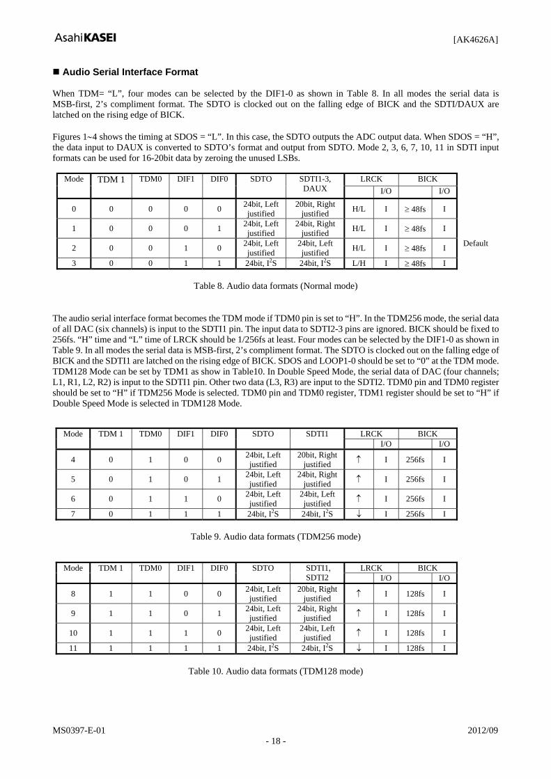
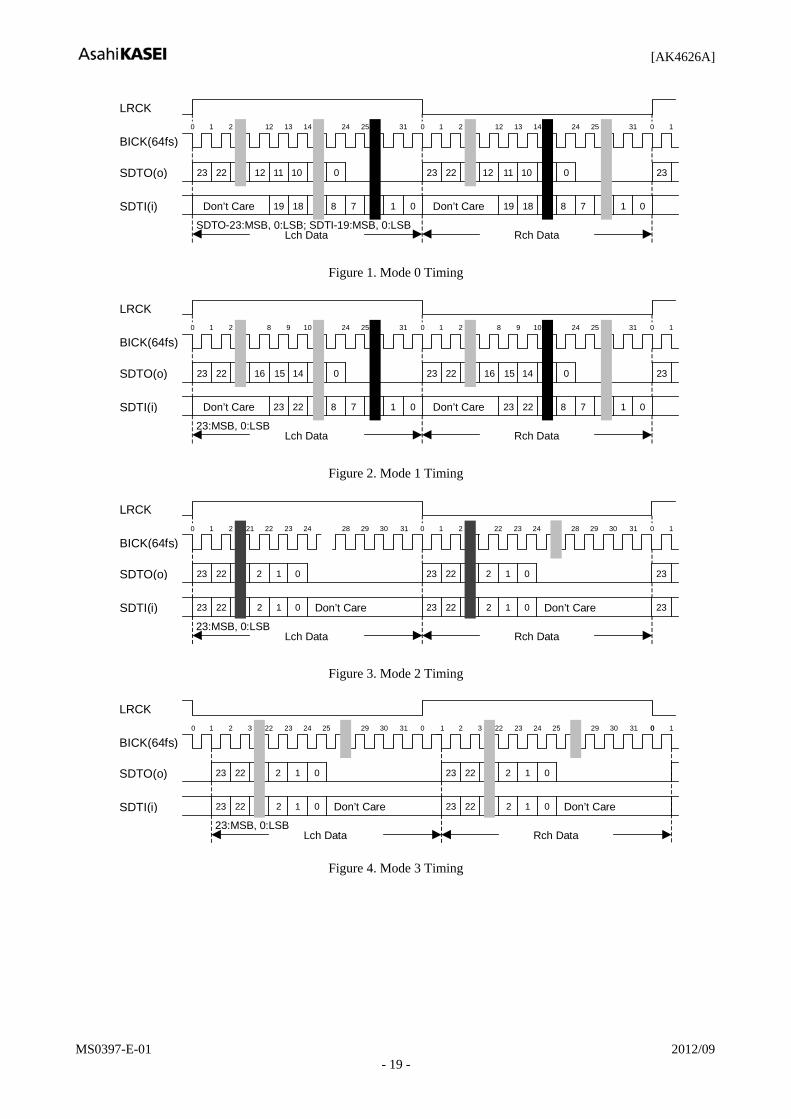
Audio Serial Interface Format When TDM= “L”, four modes can be selected by the DIF1-0 as shown in Table 8. In all modes the serial data is MSB-first, 2’s compliment format. The SDTO is clocked out on the falling edge of BICK and the SDTI/DAUX are latched on the rising edge of BICK. Figures 1∼4 shows the timing at SDOS = “L”. In this case, the SDTO outputs the ADC output data. When SDOS = “H”, the data input to DAUX is converted to SDTO’s format and output from SDTO. Mode 2, 3, 6, 7, 10, 11 in SDTI input formats can be used for 16-20bit data by zeroing the unused LSBs.
LRCK BICK Mode TDM 1 TDM0 DIF1 DIF0 SDTO SDTI1-3, DAUX I/O I/O
0 0 0 0 0 24bit, Left justified
20bit, Right justified H/L I ≥ 48fs I
1 0 0 0 1 24bit, Left justified
24bit, Right justified H/L I ≥ 48fs I
2 0 0 1 0 24bit, Left justified
24bit, Left justified H/L I ≥ 48fs I Default
3 0 0 1 1 24bit, I2S 24bit, I2S L/H I ≥ 48fs I
Table 8. Audio data formats (Normal mode) The audio serial interface format becomes the TDM mode if TDM0 pin is set to “H”. In the TDM256 mode, the serial data of all DAC (six channels) is input to the SDTI1 pin. The input data to SDTI2-3 pins are ignored. BICK should be fixed to 256fs. “H” time and “L” time of LRCK should be 1/256fs at least. Four modes can be selected by the DIF1-0 as shown in Table 9. In all modes the serial data is MSB-first, 2’s compliment format. The SDTO is clocked out on the falling edge of BICK and the SDTI1 are latched on the rising edge of BICK. SDOS and LOOP1-0 should be set to “0” at the TDM mode. TDM128 Mode can be set by TDM1 as show in Table10. In Double Speed Mode, the serial data of DAC (four channels; L1, R1, L2, R2) is input to the SDTI1 pin. Other two data (L3, R3) are input to the SDTI2. TDM0 pin and TDM0 register should be set to “H” if TDM256 Mode is selected. TDM0 pin and TDM0 register, TDM1 register should be set to “H” if Double Speed Mode is selected in TDM128 Mode.
LRCK BICK Mode TDM 1 TDM0 DIF1 DIF0 SDTO SDTI1 I/O I/O
4 0 1 0 0 24bit, Left justified
20bit, Right justified ↑ I 256fs I
5 0 1 0 1 24bit, Left justified
24bit, Right justified ↑ I 256fs I
6 0 1 1 0 24bit, Left justified
24bit, Left justified ↑ I 256fs I
7 0 1 1 1 24bit, I2S 24bit, I2S ↓ I 256fs I
Table 9. Audio data formats (TDM256 mode)
LRCK BICK Mode TDM 1 TDM0 DIF1 DIF0 SDTO SDTI1, SDTI2 I/O I/O
8 1 1 0 0 24bit, Left justified
20bit, Right justified ↑ I 128fs I
9 1 1 0 1 24bit, Left justified
24bit, Right justified ↑ I 128fs I
10 1 1 1 0 24bit, Left justified
24bit, Left justified ↑ I 128fs I
11 1 1 1 1 24bit, I2S 24bit, I2S ↓ I 128fs I
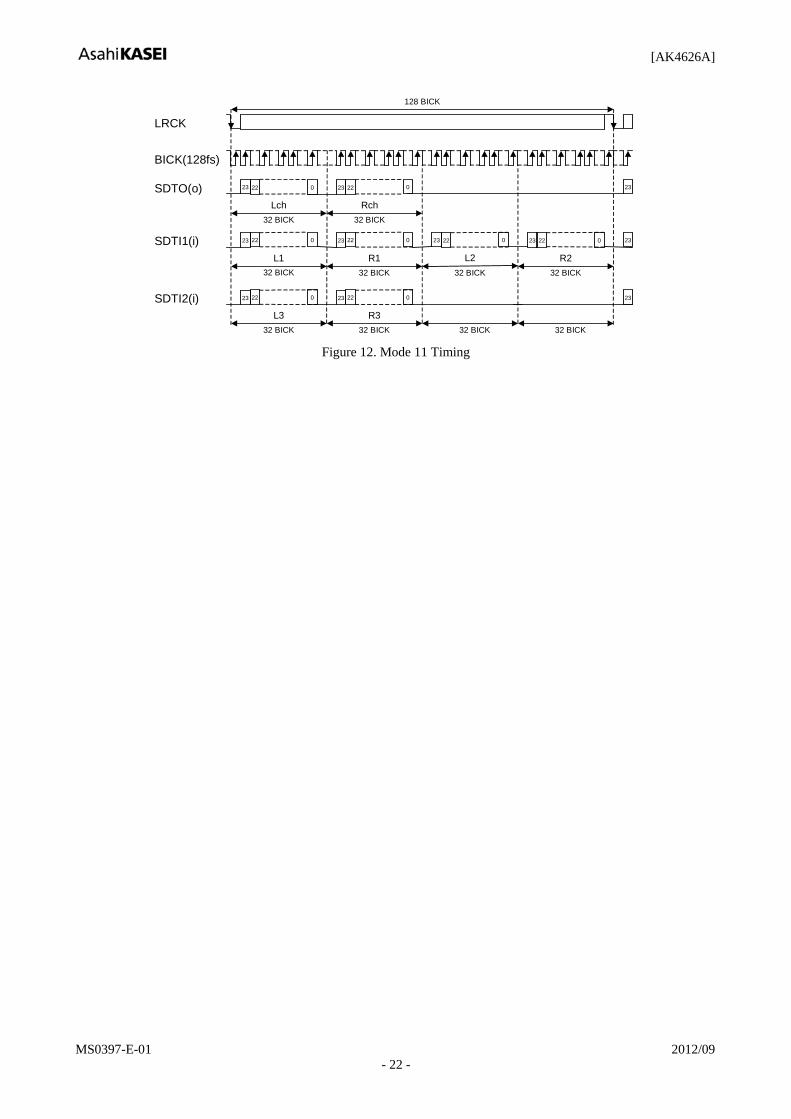
Table 10. Audio data formats (TDM128 mode)
[AK4626A]
MS0397-E-01 2012/09 - 19 -
LRCK
BICK(64fs)
SDTO(o)
0 1 2 12 13 14 24 25 31 0 1 2 12 13 14 24 25 31 0
23
1
22 0 23 22 12 11 10 0 23
SDTI(i) 118 019 8 7 118 019 8 7
Lch Data Rch Data
Don’t Care Don’t Care
12 11 10
SDTO-23:MSB, 0:LSB; SDTI-19:MSB, 0:LSB
Figure 1. Mode 0 Timing
LRCK
BICK(64fs)
SDTO(o)
0 1 2 8 9 10 24 25 31 0 1 2 8 9 10 24 25 31 0
23
1
22 0 23 22 16 15 14 0 23
SDTI(i) 122 023 8 7 122 023 8 7
23:MSB, 0:LSBLch Data Rch Data
Don’t Care Don’t Care
16 15 14
Figure 2. Mode 1 Timing
LRCK
BICK(64fs)
SDTO(o)
0 1 2 21 22 23 24 31 0 1 2 0
23
1
22 1 23 22 23
SDTI(i) 22 23 0 2223
23:MSB, 0:LSB Lch Data Rch Data
Don’t Care
2
2 1
28 29 30
23
0
22 23 24 31
1
0 Don’t Care
2
2 1
28 29 30
0
Figure 3. Mode 2 Timing
LRCK
BICK(64fs)
SDTO(o)
0 1 2 3 22 23 24 25 0 0 1
SDTI(i)
3129 30
23 22 1
22 23 0
23:MSB, 0:LSB Lch Data Rch Data
Don’t Care
2
2 1
0
2 3 22 23 24 25 031 29 30
23 22 1
2223 0 Don’t Care
2
2 1
0
1
Figure 4. Mode 3 Timing

[AK4626A]
MS0397-E-01 2012/09 - 20 -
256 BICK
BICK(256fs)
SDTO(o)
SDTI1(i)
22 0
Lch 32 BICK
18 0
L1 32 BICK
18 0
R1 32 BICK
18 0
L2 32 BICK
18 0
R2 32 BICK
18 0
L3 32 BICK
18 0
R3 32 BICK
18 0
32 BICK
18 0
32 BICK
22 0
Rch 32 BICK
22 23
19 19 19 19 19
23
19 19 19
23
19
LRCK
Figure 5. Mode 4 Timing
256 BICK
BICK(256fs)
SDTO(o)
SDTI1(i)
22 0
Lch 32 BICK
22 0
L1 32 BICK
22 0
R1 32 BICK
22 0
L2 32 BICK
22 0
R2 32 BICK
22 0
L3 32 BICK
22 0
R3 32 BICK
22 0
32 BICK
22 0
32 BICK
22 0
Rch 32 BICK
22 23
23 23 23 23 23
23
23 23 23
23
23
LRCK
Figure 6. Mode 5 Timing
256 BICK
BICK(256fs)
SDTO(o)
SDTI1(i)
22 0
Lch 32 BICK
22 0
L1 32 BICK
22 0
R1 32 BICK
22 0
L2 32 BICK
22 0
R2 32 BICK
22 0
L3 32 BICK
22 0
R3 32 BICK
22 0
32 BICK
22 0
32 BICK
22 0
Rch 32 BICK
22
22
23
23 23 23 23 23
23
23 23 23
23
23
LRCK
Figure 7. Mode 6 Timing
256 BICK
BICK(256fs)
SDTO(o)
SDTI1(i)
23 0
Lch 32 BICK
23 0
L1 32 BICK
23 0
R1 32 BICK
23 0
L2 32 BICK
23 0
R2 32 BICK
23 0
L3 32 BICK
23 0
R3 32 BICK
23 0
32 BICK
23 0
32 BICK
23 0
Rch 32 BICK
23
23
LRCK
Figure 8. Mode 7 Timing

[AK4626A]
MS0397-E-01 2012/09 - 21 -
128 BICK
BICK(128fs)
SDTO(o) 22 0
Lch 32 BICK
L1 32 BICK
R1 32 BICK
L2 32 BICK
R2 32 BICK
L3 32 BICK
R3 32 BICK
32 BICK
32 BICK
22 0
Rch 32 BICK
22 23 23 23
SDTI1(i) 18 0 18 0 18 0 18 0 19 19 19 19 19
LRCK
SDTI2(i) 18 0 18 0 18 0 18 0 19 19 19 19 19
Figure 9. Mode 8 Timing
128 BICK
BICK(128fs)
22 0
Lch 32 BICK
L1 32 BICK
R1 32 BICK
L2 32 BICK
R2 32 BICK
L3 32 BICK
R3 32 BICK
32 BICK
32 BICK
22 0
Rch 32 BICK
22 23 23 23
SDTI1(i) 22 0 22 0 22 0 22 0 23 23 23 23 19
LRCK
SDTI2(i) 22 0 22 0 22 0 22 0 23 23 23 23 19
Figure 10. Mode 9 Timing
128 BICK
BICK(128fs)
SDTO(o) 22 0
Lch 32 BICK
L1 32 BICK
R1 32 BICK
L2 32 BICK
R2 32 BICK
L3 32 BICK
R3 32 BICK
32 BICK
32 BICK
22 0
Rch 32 BICK
22 23 23 23
LRCK
SDTI1(i) 22 0 22 0 22 0 22 0 23 23 23 23 22 23
SDTI2(i) 22 0 22 0 22 0 22 0 23 23 23 23 22 23
Figure 11. Mode 10 Timing
[AK4626A]
MS0397-E-01 2012/09 - 22 -
128 BICK
BICK(128fs)
SDTO(o) 22 0
Lch 32 BICK
L1 32 BICK
R1 32 BICK
L2 32 BICK
R2 32 BICK
L3 32 BICK
R3 32 BICK
32 BICK
32 BICK
22 0
Rch 32 BICK
23 23 23
SDTI1(i) 22 0 22 0 22 0 22 0 23 23 23 23 23
SDTI2(i) 22 0 22 0 22 0 22 0 23 23 23 23 23
LRCK
Figure 12. Mode 11 Timing

[AK4626A]
MS0397-E-01 2012/09 - 23 -
Overflow Detection The AK4626A has overflow detect function for analog input. Overflow detect function is enable if OVFE bit is set to “1” at serial control mode. OVF pin goes to “H” if analog input of Lch or Rch overflows (more than -0.3dBFS). OVF output for overflowed analog input has the same group delay as ADC (GD = 16/fs = 333μs @fs=48kHz). OVF is “L” for 522/fs (=11.8ms @fs=48kHz) after PDN = “↑”, and then overflow detection is enabled.
Zero Detection The AK4626A has two pins for zero detect flag outputs. Channel grouping can be selected by DZFM3-0 bits if P/S = “L” and DZFE = “L” (Table 11). DZF1 pin corresponds to the group 1 channels and DZF2 pin corresponds to the group 2 channels. However DZF2 pin becomes OVF pin if OVFE bit is set to “1”. Zero detection mode is set to mode 0 if DZFE= “H” regardless of P/S pin. DZF1 is AND of all six channels and DZF2 is disabled (“L”) at mode 0. Table 12 shows the relation of P/S, DZFE, OVFE and DZF. When the input data of all channels in the group 1(group 2) are continuously zeros for 8192 LRCK cycles, DZF1(DZF2) pin goes to “H”. DZF1(DZF2) pin immediately goes to “L” if input data of any channels in the group 1(group 2) is not zero after going DZF1(DZF2) “H”.
DZFM AOUT Mode 3 2 1 0 L1 R1 L2 R2 L3 R3 0 0 0 0 0 DZF1 DZF1 DZF1 DZF1 DZF1 DZF1 1 0 0 0 1 DZF1 DZF1 DZF1 DZF1 DZF1 DZF2 2 0 0 1 0 DZF1 DZF1 DZF1 DZF1 DZF2 DZF2 3 0 0 1 1 DZF1 DZF1 DZF1 DZF2 DZF2 DZF2 4 0 1 0 0 DZF1 DZF1 DZF2 DZF2 DZF2 DZF2 5 0 1 0 1 DZF1 DZF2 DZF2 DZF2 DZF2 DZF2 6 0 1 1 0 DZF2 DZF2 DZF2 DZF2 DZF2 DZF2 7 0 1 1 1 disable (DZF1=DZF2 = “L”) 8 1 0 0 0 9 1 0 0 1
Not Available
10 1 0 1 0 11 1 0 1 1 12 1 1 0 0 13 1 1 0 1 14 1 1 1 0 15 1 1 1 1
disable (DZF1=DZF2 = “L”)
Default
Table 11. Zero detect control
P/S pin DZFE pin OVFE bit DZF mode DZF1 pin DZF2/OVF pin
“L” disable Mode 7 “L” “L” “H” (parallel mode) “H” disable Mode 0 AND of 6ch “L”
“0” Selectable Selectable Selectable “L” “1” Selectable Selectable OVF output “0” Mode 0 AND of 6ch “L”
“L” (serial mode)
“H” “1” Mode 0 AND of 6ch OVF output
Table 12. DZF1-2 pins outputs
[AK4626A]
MS0397-E-01 2012/09 - 24 -
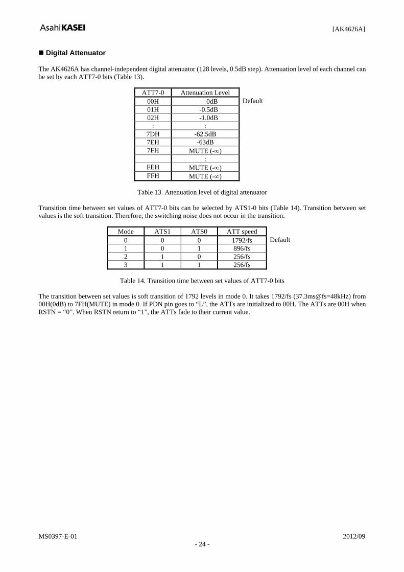
Digital Attenuator The AK4626A has channel-independent digital attenuator (128 levels, 0.5dB step). Attenuation level of each channel can be set by each ATT7-0 bits (Table 13).
ATT7-0 Attenuation Level 00H 0dB 01H -0.5dB 02H -1.0dB
: : 7DH -62.5dB 7EH -63dB 7FH MUTE (-∞)
: FEH MUTE (-∞) FFH MUTE (-∞)
Default
Table 13. Attenuation level of digital attenuator
Transition time between set values of ATT7-0 bits can be selected by ATS1-0 bits (Table 14). Transition between set values is the soft transition. Therefore, the switching noise does not occur in the transition.
Mode ATS1 ATS0 ATT speed 0 0 0 1792/fs 1 0 1 896/fs 2 1 0 256/fs 3 1 1 256/fs
Default
Table 14. Transition time between set values of ATT7-0 bits
The transition between set values is soft transition of 1792 levels in mode 0. It takes 1792/fs (37.3ms@fs=48kHz) from 00H(0dB) to 7FH(MUTE) in mode 0. If PDN pin goes to “L”, the ATTs are initialized to 00H. The ATTs are 00H when RSTN = “0”. When RSTN return to “1”, the ATTs fade to their current value.

[AK4626A]
MS0397-E-01 2012/09 - 25 -
Soft mute operation Soft mute operation is performed at digital domain. When the SMUTE pin goes to “H”, the output signal is attenuated by -∞ during ATT_DATA×ATT transition time (Table 14) from the current ATT level. When the SMUTE pin is returned to “L”, the mute is cancelled and the output attenuation gradually changes to the ATT level during ATT_DATA×ATT transition time. If the soft mute is cancelled before attenuating to -∞ after starting the operation, the attenuation is discontinued and returned to ATT level by the same cycle. The soft mute is effective for changing the signal source without stopping the signal transmission.
SMUTE bit
Attenuation
DZF1,2
ATT Level
-∞
AOUT
8192/fs
GD GD
(1)
(2)
(3)
(4)
(1)
Notes:
(1) ATT_DATA×ATT transition time (Table 14). For example, in Normal Speed Mode, this time is 1792LRCK cycles (1792/fs) at ATT_DATA=00H. ATT transition of the soft-mute is from 00H to 7FH
(2) The analog output corresponding to the digital input has a group delay, GD. (3) If the soft mute is cancelled before attenuating to -∞ after starting the operation, the attenuation is discontinued and
returned to ATT level by the same cycle. (4) When the input data at all the channels of the group are continuously zeros for 8192 LRCK cycles, DZF pin of each
channel goes to “H”. DZF pin immediately goes to “L” if the input data of either channel of the group are not zero after going DZF “H”.
Figure 13. Soft mute and zero detection
System Reset The AK4626A should be reset once by bringing PDN = “L” upon power-up. The AK4626A is powered up and the internal timing starts clocking by LRCK “↑” after exiting reset and power down state by MCLK. The AK4626A is in the power-down mode until MCLK and LRCK are input.

[AK4626A]
MS0397-E-01 2012/09 - 26 -
Power-Down The ADC and DACs of AK4626A are placed in the power-down mode by bringing PDN “L” and both digital filters are reset at the same time. PDN “L” also reset the control registers to their default values. In the power-down mode, the analog outputs go to VCOM voltage and DZF1-2 pins go to “L”. This reset should always be done after power-up. In case of the ADC, an analog initialization cycle starts after exiting the power-down mode. Therefore, the output data, SDTO becomes available after 522 cycles of LRCK clock. In case of the DAC, an analog initialization cycle starts after exiting the power-down mode. The analog outputs are VCOM voltage during the initialization. Figure 14 shows the sequences of the power-down and the power-up. The ADC and all DACs can be powered-down individually by PWADN and PWDAN bits. In this case, the internal register values are not initialized. When PWADN = “0”, SDTO goes to “L”. When PWDAN = “0”, the analog outputs go to VCOM voltage and DZF1-2 pins go to “H”. Because some click noise occurs, the analog output should muted externally if the click noise influences system application.
ADC Internal State
PDN522/fs
Normal Operation Power-down Init Cycle Normal Operation
(1)
Don’t care
GD GD
Clock InMCLK,LRCK,SCLK
ADC In (Analog)
“0”dataADC Out (Digital)
Normal Operation Power-down Normal OperationDAC Internal State
“0”dataDAC In (Digital)
DAC Out (Analog)
GD
External Mute Mute ON
GD
(3)
(3)
(4)(5)
(6) (6)
(9)
516/fs
Init Cycle
(2)
DZF1/DZF2
(7)
(8)
10∼11/fs (10)
Notes:
(1) The analog part of ADC is initialized after exiting the power-down state. (2) The analog part of DAC is initialized after exiting the power-down state. (3) Digital output corresponding to analog input and analog output corresponding to digital input have the group delay
(GD). (4) ADC output is “0” data at the power-down state. (5) Click noise occurs at the end of initialization of the analog part. Please mute the digital output externally if the click
noise influences system application. (6) Click noise occurs at the falling edge of PDN and at 512/fs after the rising edge of PDN. (7) When the external clocks (MCLK, BICK and LRCK) are stopped, the AK4626A should be in the power down mode. (8) DZF pins are “L” in the power-down mode (PDN = “L”). (9) Please mute the analog output externally if the click noise (6) influences system application. (10) DZF= “L” for 10∼11/fs after PDN= “↑”.
Figure 14. Power-down/up sequence example

[AK4626A]
MS0397-E-01 2012/09 - 27 -
Reset Function When RSTN = “0”, ADC and DACs are powered-down but the internal register are not initialized. The analog outputs go to VCOM voltage, DZF1-2 pins go to “H” and SDTO pin goes to “L”. Because some click noise occurs, the analog output should muted externally if the click noise influences system application. Figure 15 shows the power-up sequence.
ADC Internal State
RSTN bit
Normal Operation Digital Block Power-down Normal Operation
Don’t care
GD GD
Clock InMCLK,LRCK,SCLK
ADC In (Analog)
“0”dataADC Out (Digital)
Normal Operation Normal OperationDAC Internal State
“0”dataDAC In (Digital)
DAC Out (Analog)
GD GD
(2)
(2)
(3)(4)
(6) (6)
DZF1/DZF2
(7)
InternalRSTN bit
Digital Block Power-down
1~2/fs (9)4~5/fs (9)
4∼5/fs (8)
(5)
516/fs
Init Cycle
(1)
Notes:
(1) The analog part of ADC is initialized after exiting the reset state. (2) Digital output corresponding to analog input and analog output corresponding to digital input have the group delay
(GD). (3) ADC output is “0” data at the power-down state. (4) Click noise occurs when the internal RSTN bit becomes “1”. Please mute the digital output externally if the click
noise influences system application. (5) The analog outputs go to VCOM voltage. (6) Click noise occurs at 4∼5/fs after RSTN bit becomes “0”, and occurs at 1∼2/fs after RSTN bit becomes “1”. This
noise is output even if “0” data is input. (7) The external clocks (MCLK, BICK and LRCK) can be stopped in the reset mode. When exiting the reset mode, “1”
should be written to RSTN bit after the external clocks (MCLK, BICK and LRCK) are fed. (8) DZF pins go to “H” when the RSTN bit becomes “0”, and go to “L” at 6~7/fs after RSTN bit becomes “1”. (9) There is a delay, 4~5/fs from RSTN bit “0” to the internal RSTN bit “0”.
Figure 15. Reset sequence example

[AK4626A]
MS0397-E-01 2012/09 - 28 -
Serial Control Interface The AK4626A can control its functions via registers. Internal registers may be written by 2 types of control mode. The chip address is determined by the state of the CAD0 and CAD1 inputs. PDN = “L” initializes the registers to their default values. Writing “0” to the RSTN bit can initialize the internal timing circuit. But in this case, the register data is not be initialized. When the state of P/S pin is changed, the AK4626A should be reset by PDN pin.
* Writing to control register is invalid when PDN = “L”. * AK4626A does not support the read command.
(1) 3-wire Serial Control Mode (I2C = “L”)
Internal registers may be written to the 3 wire µP interface pins (CSN, CCLK and CDTI). The data on this interface consists of Chip address (2bits, CAD0/1), Read/Write (1bit, Fixed to “1”, Write only), Register address (MSB first, 5bits) and Control data (MSB first, 8bits). Address and data is clocked in on the rising edge of CCLK and data is clocked out on the falling edge. For write operations, data is latched after a low-to-high transition of CSN. The clock speed of CCLK is 5MHz(max).
CDTI
CCLK
CSN
C1
0 1 2 3 4 5 6 7 8 9 10 11 12 13 14 15
D4D5D6D7A1A2A3A4R/WC0 A0 D0D1D2D3
C1-C0: Chip Address (C1=CAD1, C0=CAD0) R/W: Read/Write (Fixed to “1”, Write only) A4-A0: Register Address D7-D0: Control Data
Figure 16. 3-wire Serial Control I/F Timing

[AK4626A]
MS0397-E-01 2012/09 - 29 -
(2) I2C-bus Control Mode (I2C= “H”) AK4626A supports the standard-mode I2C-bus (max:100kHz). Then AK4626A does not support a fast-mode I2C-bus system (max:400kHz). The CSN pin should be connected to DVDD at the I2C-bus mode. Figure 17 shows the data transfer sequence at the I2C-bus mode. All commands are preceded by a START condition. A HIGH to LOW transition on the SDA line while SCL is HIGH indicates a START condition (Figure 21). After the START condition, a slave address is sent. This address is 7 bits long followed by an eighth bit which is a data direction bit (R/W) (Figure 18). The most significant five bits of the slave address are fixed as “00100”. The next two bits are CAD1 and CAD0 (device address bits). These two bits identify the specific device on the bus. The hard-wired input pins (CAD1 pin and CAD0 pin) set them. If the slave address match that of the AK4626A and R/W bit is “0”, the AK4626A generates the acknowledge and the write operation is executed. If R/W bit is “1”, the AK4626A generates the not acknowledge since the AK4626A can be only a slave-receiver. The master must generate the acknowledge-related clock pulse and release the SDA line (HIGH) during the acknowledge clock pulse (Figure 22). The second byte consists of the address for control registers of the AK4626A. The format is MSB first, and those most significant 3-bits are fixed to zeros (Figure 20). Those data after the second byte contain control data. The format is MSB first, 8bits (Figure 20). The AK4626A generates an acknowledge after each byte has been received. A data transfer is always terminated by a STOP condition generated by the master. A LOW to HIGH transition on the SDA line while SCL is HIGH defines a STOP condition (Figure 20). The AK4626A is capable of more than one byte write operation by one sequence. After receipt of the third byte, the AK4626A generates an acknowledge, and awaits the next data again. The master can transmit more than one byte instead of terminating the write cycle after the first data byte is transferred. After the receipt of each data, the internal 5bits address counter is incremented by one, and the next data is taken into next address automatically. If the address exceed 1FH prior to generating the stop condition, the address counter will “roll over” to 00H and the previous data will be overwritten. The data on the SDA line must be stable during the HIGH period of the clock. The HIGH or LOW state of the data line can only change when the clock signal on the SCL line is LOW (Figure 23) except for the START and the STOP condition.
SDA
START
ACK
ACK
S SlaveAddress
ACK
SubAddress(n) Data(n) P
STOP
Data(n+x)
ACK
Data(n+1)
ACK
R/W
ACK
Figure 17. Data transfer sequence at the I2C-bus mode
0 0 1 0 0 CAD1 CAD0 R/W
(Those CAD1/0 should match with CAD1/0 pins) Figure 18. The first byte
* * * A4 A3 A2 A1 A0
(*: Don’t care) Figure 19. The second byte
D7 D6 D5 D4 D3 D2 D1 D0
Figure 20. Byte structure after the second byte

[AK4626A]
MS0397-E-01 2012/09 - 30 -
SCL
SDA
stop conditionstart condition
S P
Figure 21. START and STOP conditions
SCL FROMMASTER
acknowledge
DATAOUTPUT BYMASTER
DATAOUTPUT BYSLAVE(AK4529)
1 98
STARTCONDITION
not acknowledge
clock pulse foracknowledgement
S
2
Figure 22. Acknowledge on the I2C-bus
SCL
SDA
data linestable;
data valid
changeof dataallowed
Figure 23. Bit transfer on the I2C-bus

[AK4626A]
MS0397-E-01 2012/09 - 31 -
Mapping of Program Registers
Addr Register Name D7 D6 D5 D4 D3 D2 D1 D0 00H Control 1 0 0 TDM1 TDM0 DIF1 DIF0 0 SMUTE01H Control 2 0 DFS1 LOOP1 LOOP0 SDOS DFS0 ACKS 0 02H LOUT1 Volume Control ATT7 ATT6 ATT5 ATT4 ATT3 ATT2 ATT1 ATT0 03H ROUT1 Volume Control ATT7 ATT6 ATT5 ATT4 ATT3 ATT2 ATT1 ATT0 04H LOUT2 Volume Control ATT7 ATT6 ATT5 ATT4 ATT3 ATT2 ATT1 ATT0 05H ROUT2 Volume Control ATT7 ATT6 ATT5 ATT4 ATT3 ATT2 ATT1 ATT0 06H LOUT3 Volume Control ATT7 ATT6 ATT5 ATT4 ATT3 ATT2 ATT1 ATT0 07H ROUT3 Volume Control ATT7 ATT6 ATT5 ATT4 ATT3 ATT2 ATT1 ATT0 08H De-emphasis 0 0 DEMA1 DEMA0 DEMB1 DEMB0 DEMC1 DEMC009H ATT speed & Reset
Control 0 0 ATS1 ATS0 0 0 0 RSTN
0AH Zero detect OVFE DZFM3 DZFM2 DZFM1 DZFM0 PWVRN PWADN PWDAN Note: For addresses from 0BH to 1FH, data is not written.
When PDN goes to “L”, the registers are initialized to their default values. When RSTN bit goes to “0”, the internal timing is reset and DZF1-2 pins go to “H”, but registers are not initialized to their default values. SMUTE, DFS0, SDOS and TDM0 are ORed with pins.
[AK4626A]
MS0397-E-01 2012/09 - 32 -
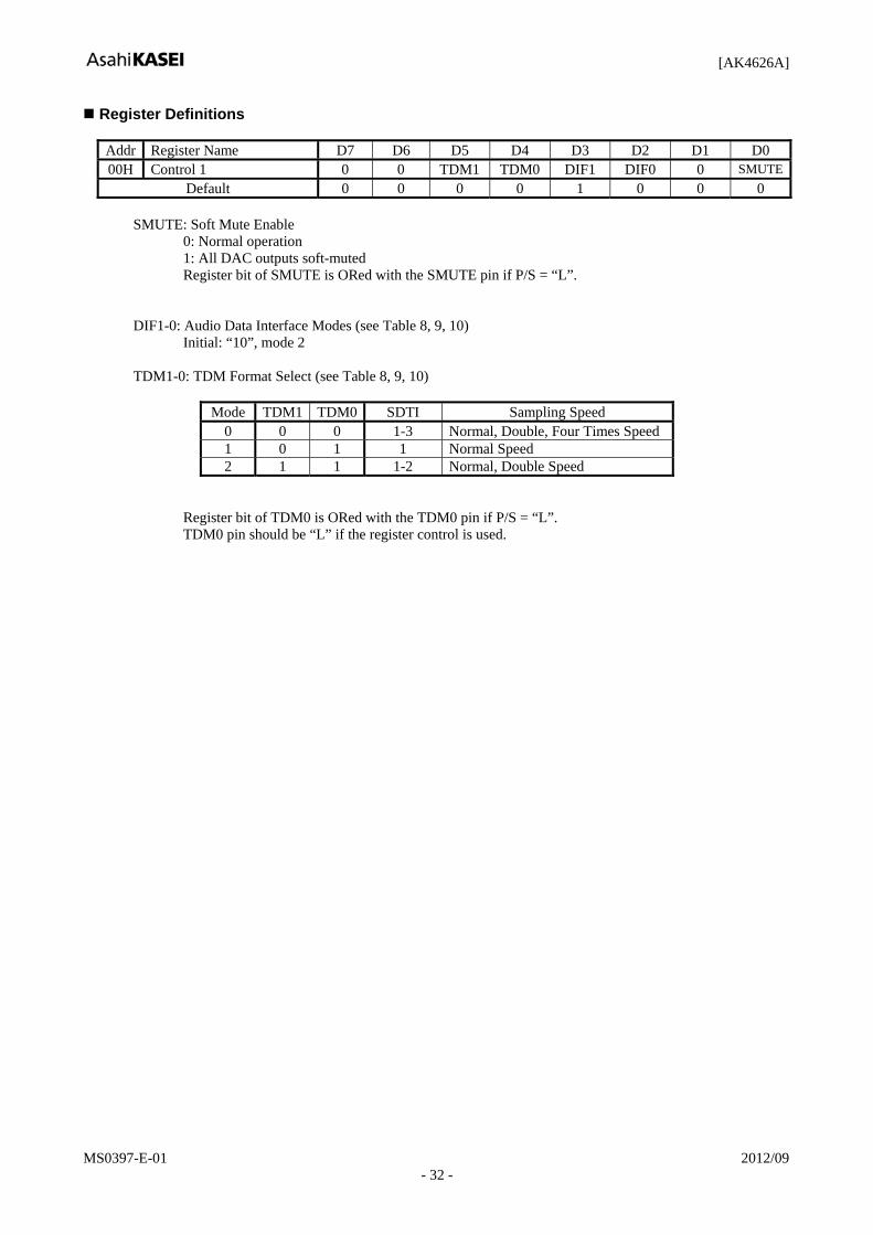
Register Definitions
Addr Register Name D7 D6 D5 D4 D3 D2 D1 D0 00H Control 1 0 0 TDM1 TDM0 DIF1 DIF0 0 SMUTE
Default 0 0 0 0 1 0 0 0 SMUTE: Soft Mute Enable 0: Normal operation 1: All DAC outputs soft-muted Register bit of SMUTE is ORed with the SMUTE pin if P/S = “L”.
DIF1-0: Audio Data Interface Modes (see Table 8, 9, 10) Initial: “10”, mode 2 TDM1-0: TDM Format Select (see Table 8, 9, 10)
Mode TDM1 TDM0 SDTI Sampling Speed 0 0 0 1-3 Normal, Double, Four Times Speed 1 0 1 1 Normal Speed 2 1 1 1-2 Normal, Double Speed
Register bit of TDM0 is ORed with the TDM0 pin if P/S = “L”. TDM0 pin should be “L” if the register control is used.

[AK4626A]
MS0397-E-01 2012/09 - 33 -
Addr Register Name D7 D6 D5 D4 D3 D2 D1 D0 01H Control 2 0 DFS1 LOOP1 LOOP0 SDOS DFS0 ACKS 0
Default 0 0 0 0 0 0 0 0
ACKS: Master Clock Frequency Auto Setting Mode Enable 0: Disable, Manual Setting Mode 1: Enable, Auto Setting Mode Master clock frequency is detected automatically at ACKS bit “1”. In this case, the setting of DFS are ignored. When this bit is “0”, DFS0, 1 set the sampling speed mode.
DFS1-0: Sampling speed mode (see Table 1.)
Register bit of DFS0 is ORed with DFS0 pin if P/S = “L”. The setting of DFS is ignored at ACKS bit “1”.
SDOS: SDTO source select 0: ADC 1: DAUX Register bit of SDOS is ORed with SDOS pin if P/S = “L”.
SDOS should be set to “0” at TDM bit “1”. In the case of PWADN=”0” and PWDAN=”0”, the setting of SDOS becomes invalid. And ADC is selected. The output of SDTO becomes “L” at PWADN=”0”.
LOOP1-0: Loopback mode enable 00: Normal (No loop back) 01: LIN → LOUT1, LOUT2, LOUT3
RIN → ROUT1, ROUT2, ROUT3 The digital ADC output (DAUX input if SDOS = “1”) is connected to the digital DAC input. In this mode, the input DAC data to SDTI1-3 is ignored. The audio format of SDTO at loopback mode becomes mode 2 at mode 0, and mode 3 at mode 1, respectively.
10: SDTI1(L) → SDTI2(L), SDTI3(L) SDTI1(R) → SDTI2(R), SDTI3(R) In this mode the input DAC data to SDTI2-3 is ignored. 11: N/A
LOOP1-0 should be set to “00” at TDM bit “1”. In the case of PWADN=”0” and PWDAN=”0”, the setting of LOOP1-0 becomes invalid. And ADC is selected. And it becomes the normal operation (No loop back).

[AK4626A]
MS0397-E-01 2012/09 - 34 -
Addr Register Name D7 D6 D5 D4 D3 D2 D1 D0 02H LOUT1 Volume Control ATT7 ATT6 ATT5 ATT4 ATT3 ATT2 ATT1 ATT003H ROUT1 Volume Control ATT7 ATT6 ATT5 ATT4 ATT3 ATT2 ATT1 ATT004H LOUT2 Volume Control ATT7 ATT6 ATT5 ATT4 ATT3 ATT2 ATT1 ATT005H ROUT2 Volume Control ATT7 ATT6 ATT5 ATT4 ATT3 ATT2 ATT1 ATT006H LOUT3 Volume Control ATT7 ATT6 ATT5 ATT4 ATT3 ATT2 ATT1 ATT007H ROUT3 Volume Control ATT7 ATT6 ATT5 ATT4 ATT3 ATT2 ATT1 ATT0
Default 0 0 0 0 0 0 0 0 ATT7-0: Attenuation Level (see Table 13.)
Addr Register Name D7 D6 D5 D4 D3 D2 D1 D0 08H De-emphasis 0 0 DEMA1 DEMA0 DEMB1 DEMB0 DEMC1 DEMC0
Default 0 0 0 1 0 1 0 1 DEMA1-0: De-emphasis response control for DAC1 data on SDTI1 (see Table 7.) Initial: “01”, OFF DEMB1-0: De-emphasis response control for DAC2 data on SDTI2 (see Table 7.) Initial: “01”, OFF DEMC1-0: De-emphasis response control for DAC3 data on SDTI3 (see Table 7.) Initial: “01”, OFF
[AK4626A]
MS0397-E-01 2012/09 - 35 -
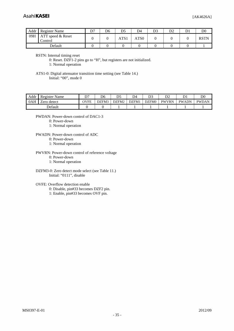
Addr Register Name D7 D6 D5 D4 D3 D2 D1 D0 09H ATT speed & Reset
Control 0 0 ATS1 ATS0 0 0 0 RSTN
Default 0 0 0 0 0 0 0 1 RSTN: Internal timing reset
0: Reset. DZF1-2 pins go to “H”, but registers are not initialized. 1: Normal operation ATS1-0: Digital attenuator transition time setting (see Table 14.) Initial: “00”, mode 0
Addr Register Name D7 D6 D5 D4 D3 D2 D1 D0 0AH Zero detect OVFE DZFM3 DZFM2 DZFM1 DZFM0 PWVRN PWADN PWDAN
Default 0 0 1 1 1 1 1 1 PWDAN: Power-down control of DAC1-3 0: Power-down 1: Normal operation PWADN: Power-down control of ADC 0: Power-down 1: Normal operation PWVRN: Power-down control of reference voltage 0: Power-down 1: Normal operation DZFM3-0: Zero detect mode select (see Table 11.) Initial: “0111”, disable
OVFE: Overflow detection enable 0: Disable, pin#33 becomes DZF2 pin. 1: Enable, pin#33 becomes OVF pin.

[AK4626A]
MS0397-E-01 2012/09 - 36 -
SYSTEM DESIGN Figure 24 shows the system connection diagram. An evaluation board is available which demonstrates application circuits, the optimum layout, power supply arrangements and measurement results.
Condition: TVDD=5V, 3-wire serial control mode, CAD1-0 = “00”
TDM
044
43
42
41
40
39
38
37
36
35
34
SDOS 1
2
3
4
5
6
7
8
9
11
10
I2C
BICK
LRCK
SDTI1
SDTI2
SDTI3
SDTO
DAUX
DFS0
RIN
CD
TI
CC
LK
MC
LK
DZF
1
AVS
S
VR
EFH
AVD
D
VC
OM
TST1
DZF2 33
32
31
30
29
28
27
26
25
24
23
12
13
14
15
16
17
18
19
20
21
22 D
VD
D
DZF
E
TVD
D
DV
SS
TST2
CA
D1
CA
D0
TST3
TST4
LIN
NC
TST5
ROUT1
LOUT1
ROUT2
LOUT2
ROUT3
LOUT3
AK4626A
+
0.1u
0.1u2.2u
+
5
uP
Analog Ground Digital Ground
(DIR)
DSP
Analog 5V
+10u
Audio
(MPEG/ AC3)
Digital Audio Source
PD
N
CS
N
P/S
SMUTE
0.1u10u
MUTE
MUTE
MUTE
MUTE
MUTE
MUTE
Power-down control
Figure 24. Typical Connection Diagram
[AK4626A]
MS0397-E-01 2012/09 - 37 -
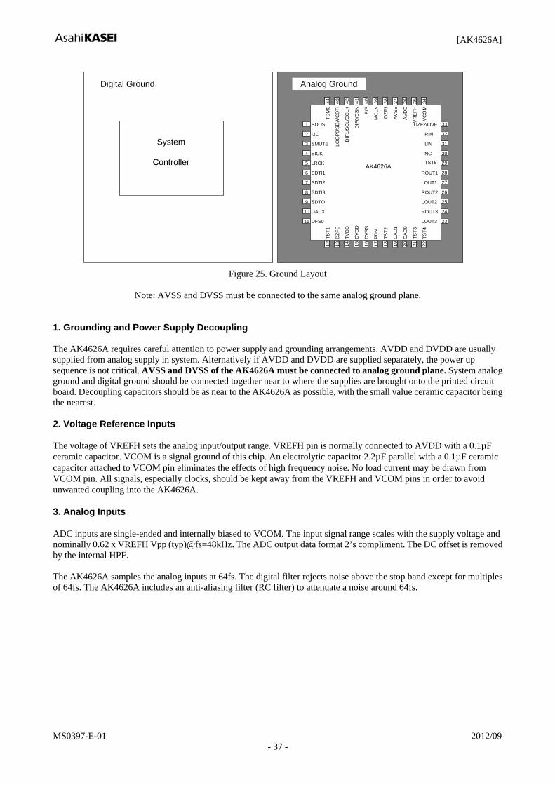
Analog Ground Digital Ground
System
Controller
TDM
0
SDOS1
2
3
4
5
6
7
8
9
11
10
I2C
BICK
LRCK
SDTI1
SDTI2
SDTI3
SDTO
DAUX
DFS0
RIN
LOO
P0/
SDA
/CD
TI
DIF
1/S
CL/
CC
L K
MC
LK
DZF
1
AVS
S
VR
EFH
AVD
D
VC
OM
TST1
DZF2/OVF
12
13
14
15
16
17 18
19
20
21
22 D
VD
D
DZF
E
TVD
D
DV
SS
TST2
CA
D1
CA
D0
TST3
TST4
LIN
NC
TST5
ROUT1
LOUT1
ROUT2
LOUT2
ROUT3
LOUT3
AK4626A
PD
N
DIF
0/C
SN P/S
SMUTE
33
32
31
30
29
28
27
26
25
23
24
44
43
42
41
40
39 38
37
36
35
34
Figure 25. Ground Layout
Note: AVSS and DVSS must be connected to the same analog ground plane.
1. Grounding and Power Supply Decoupling The AK4626A requires careful attention to power supply and grounding arrangements. AVDD and DVDD are usually supplied from analog supply in system. Alternatively if AVDD and DVDD are supplied separately, the power up sequence is not critical. AVSS and DVSS of the AK4626A must be connected to analog ground plane. System analog ground and digital ground should be connected together near to where the supplies are brought onto the printed circuit board. Decoupling capacitors should be as near to the AK4626A as possible, with the small value ceramic capacitor being the nearest. 2. Voltage Reference Inputs The voltage of VREFH sets the analog input/output range. VREFH pin is normally connected to AVDD with a 0.1µF ceramic capacitor. VCOM is a signal ground of this chip. An electrolytic capacitor 2.2µF parallel with a 0.1µF ceramic capacitor attached to VCOM pin eliminates the effects of high frequency noise. No load current may be drawn from VCOM pin. All signals, especially clocks, should be kept away from the VREFH and VCOM pins in order to avoid unwanted coupling into the AK4626A. 3. Analog Inputs ADC inputs are single-ended and internally biased to VCOM. The input signal range scales with the supply voltage and nominally 0.62 x VREFH Vpp (typ)@fs=48kHz. The ADC output data format 2’s compliment. The DC offset is removed by the internal HPF. The AK4626A samples the analog inputs at 64fs. The digital filter rejects noise above the stop band except for multiples of 64fs. The AK4626A includes an anti-aliasing filter (RC filter) to attenuate a noise around 64fs.

[AK4626A]
MS0397-E-01 2012/09 - 38 -
4. Analog Outputs The analog outputs are also single-ended and centered around the VCOM voltage. The input signal range scales with the supply voltage and nominally 0.6 x VREFH Vpp. The DAC input data format is 2’s complement. The output voltage is a positive full scale for 7FFFFFH(@24bit) and a negative full scale for 800000H(@24bit). The ideal output is VCOM voltage for 000000H(@24bit). The internal analog filters remove most of the noise generated by the delta-sigma modulator of DAC beyond the audio passband. DC offsets on analog outputs are eliminated by AC coupling since DAC outputs have DC offsets of a few mV.
Peripheral I/F Example The AK4626A can accept the signal of device with a nominal 3.3V supply because of TTL input. The power supply for output buffer (TVDD) of the AK4626A should be 3.3V when the peripheral devices operate at a nominal 3.3V supply. Figure 26 shows an example with the mixed system of 3.3V and 5V.
3.3V Analog
5V Analog
3.3V Digital
5V Digital
PLL I/F
Audio signal
DSP
AK4112B
Analog Digital
Control signal
uP &Others
AK4626A
5V for input
3.3V for output
Figure 26. Power supply connection example

[AK4626A]
MS0397-E-01 2012/09 - 39 -
PACKAGE
0.15
0.09 ~ 0.20 0.37±0.10
10.0
1.70max
1 11
2333
44pin LQFP (Unit: mm)
10.0
12.0
34
44
0.80
22
1212
.0
0 ~ 0.2
0°∼10°
0.60±0.20
Package & Lead frame material Package molding compound: Epoxy Lead frame material: Cu Lead frame surface treatment: Solder (Pb free) plate
[AK4626A]
MS0397-E-01 2012/09 - 40 -
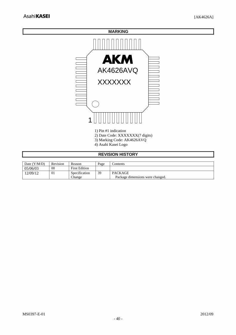
MARKING
AK4626AVQXXXXXXX
1
1) Pin #1 indication 2) Date Code: XXXXXXX(7 digits) 3) Marking Code: AK4626AVQ 4) Asahi Kasei Logo
REVISION HISTORY
Date (Y/M/D) Revision Reason Page Contents 05/06/03 00 First Edition 12/09/12 01 Specification
Change 39 PACKAGE
Package dimensions were changed.
[AK4626A]
MS0397-E-01 2012/09 - 41 -
IMPORTANT NOTICE
These products and their specifications are subject to change without notice. When you consider any use or application of these products, please make inquiries the sales office of Asahi Kasei Microdevices Corporation (AKM) or authorized distributors as to current status of the products.
Descriptions of external circuits, application circuits, software and other related information contained in this document are provided only to illustrate the operation and application examples of the semiconductor products. You are fully responsible for the incorporation of these external circuits, application circuits, software and other related information in the design of your equipments. AKM assumes no responsibility for any losses incurred by you or third parties arising from the use of these information herein. AKM assumes no liability for infringement of any patent, intellectual property, or other rights in the application or use of such information contained herein.
Any export of these products, or devices or systems containing them, may require an export license or other official approval under the law and regulations of the country of export pertaining to customs and tariffs, currency exchange, or strategic materials.
AKM products are neither intended nor authorized for use as critical componentsNote1) in any safety, life support, or other hazard related device or systemNote2), and AKM assumes no responsibility for such use, except for the use approved with the express written consent by Representative Director of AKM. As used here:
Note1) A critical component is one whose failure to function or perform may reasonably be expected to result, whether directly or indirectly, in the loss of the safety or effectiveness of the device or system containing it, and which must therefore meet very high standards of performance and reliability. Note2) A hazard related device or system is one designed or intended for life support or maintenance of safety or for applications in medicine, aerospace, nuclear energy, or other fields, in which its failure to function or perform may reasonably be expected to result in loss of life or in significant injury or damage to person or property.
It is the responsibility of the buyer or distributor of AKM products, who distributes, disposes of, or otherwise places the product with a third party, to notify such third party in advance of the above content and conditions, and the buyer or distributor agrees to assume any and all responsibility and liability for and hold AKM harmless from any and all claims arising from the use of said product in the absence of such notification.