high power radio frequency solid-state amplifiers and...
TRANSCRIPT

ACTAUNIVERSITATIS
UPSALIENSISUPPSALA
2019
Digital Comprehensive Summaries of Uppsala Dissertationsfrom the Faculty of Science and Technology 1881
High Power Radio FrequencySolid-State Amplifiers andCombiners for ParticleAccelerators
From module to system design approach
LONG HOANG
ISSN 1651-6214ISBN 978-91-513-0818-0urn:nbn:se:uu:diva-397500

Dissertation presented at Uppsala University to be publicly examined in Häggsalen,Ångströmlaboratoriet, Lägerhyddsvägen 1, Uppsala, Wednesday, 15 January 2020 at 09:15 forthe degree of Doctor of Philosophy. The examination will be conducted in English. Facultyexaminer: Professor Paul Tasker (School of Engineering, Cardiff University).
AbstractHoang, L. 2019. High Power Radio Frequency Solid-State Amplifiers and Combiners forParticle Accelerators. From module to system design approach. Digital ComprehensiveSummaries of Uppsala Dissertations from the Faculty of Science and Technology 1881. 98 pp.Uppsala: Acta Universitatis Upsaliensis. ISBN 978-91-513-0818-0.
The rise of Big Science projects brings issues related to the energy consumption and theassociated environmental impacts of such large-scale facilities. Therefore, environmentally-sustainable developments are undertaken towards the adoption of energy savings and improvedenergy-efficient approaches. The advent of the superconducting (SC) radio frequency (RF)accelerating cavity is bringing answers to these issues. Such superconducting RF (SRF) cavityis made of niobium that allows much higher accelerating gradients with a minimization ofthe energy consumption. The SC RF technology is increasingly used in many modern particleaccelerators, including: the European Spallation Source (ESS), the X-ray Free Electron Laser(XFEL), the Linac Coherent Light Source (LCLS)-II and the proposed International LinearCollider (ILC).
The innovation of solid state PA technology pushes limits regarding packaging, efficiency,frequency capability, thermal stability, making them more attractive than other well-establishedalternative technologies, such as vacuum tube technology in mid-range power applications.Through the investigations of designs and techniques, this research goal of the thesis allows toimprove solid-state based power generation systems from module to the overall system design.This thesis introduces the single-ended PA design approach in planar technology and at kilowattlevel. The design solution unlocks different possibilities including: improved integration, layoutflexibility for tuning, and suitably for mass productions that are demanded in future highpeak power generation systems. The novel amplifier design is followed by time domaincharacterization to fully evaluate the pulse profiles of such amplifiers when delivering kilowattoutput power level for operation in conjunction with SRF accelerating cavities. Amplitude andphase stability of those amplifiers are also investigated in time-domain. The extracted data canthen be used as measurement-based model for predicting factors which could degrade the overallstability of the associated PA.
Future RF power generation systems built around solid state PAs need also efficientcombining strategies. Two engineering design solutions are investigated in this thesis aimingfor mid- and high- range power combination. One solution is based on a combination of theGysel structure using suspended strip-line technology for improved power handling capability.Another solution is implementing a radial combiner, which uses re-entrant cavity resonatorat 352 MHz and door-nob geometry for coupling at inputs and at the output. These solutionsfacilitate the scaling up 400 kW for powering ESS spoke cavities while maintaining a highdegree of efficiency in RF power generation. This thesis gives insights of system integrationand tuning procedures with a demonstration of combining 8 modules, delivering a total of 10kW output power. Along with the proposed combining solutions at higher power levels, thenominal power block of 10 kW is used as an elementary block to propose scaling up in powertill the 400 kW nominal power required by ESS.
Finally, this thesis focuses on implementing an optimal charging scheme for SRF cavities,which helps reducing the wasted energy and improves the overall efficiency operation at futureaccelerating facilities. Therefore, these results contribute further to the larger adoption of solidstate technologies in the future power generation systems for particle accelerators.
Keywords: solid state technology, power amplifier, superconducting cavities, optimalcharging, high efficiency, particle accelerators
Long Hoang, Department of Engineering Sciences, Solid State Electronics, Box 534, UppsalaUniversity, SE-75121 Uppsala, Sweden. Department of Physics and Astronomy, FREIA, Box516, Uppsala University, SE-751 20 Uppsala, Sweden.
© Long Hoang 2019ISSN 1651-6214ISBN 978-91-513-0818-0urn:nbn:se:uu:diva-397500 (http://urn.kb.se/resolve?urn=urn:nbn:se:uu:diva-397500)

Dành cho bố mẹ, và vợ Dương Ngọc HươngDedicated to my parents, and my wife Duong Ngoc Huong
”Move fast, and break things” Mark Zuckerberg


List of papers
This thesis is based on the following papers, which are referred to in the textby their Roman numerals.
I Linus Haapala, Aleksander Eriksson, Long Hoang Duc and DragosDancila, "Kilowatt-level power amplifier in a single-ended
architecture at 352 MHz," in Electronics Letters, vol. 52, no. 18,pp. 1552-1554, 2016.
II Long Hoang Duc, Anirban Bhattacharyya, Vitaliy Goryasko, RogerRuber, Anders Rydberg, Jorgen Olsson, and Dragos Dancila, "Time
domain characterization of high power solid state amplifiers for
the next generation linear accelerators," in Microwave and OpticalTechnology Letters, vol. 60, no. 1, pp. 163–171, 2018.
III Long Hoang Duc, Anh Nguyen Dinh The, Duong Bach Gia, MagnusJobs, Roger Ruber and Dragos Dancila, "High-power low-loss
air-dielectric stripline Gysel divider/combiner for particle
accelerator applications at 352 MHz," in The Journal ofEngineering, vol. 2018, no. 5, pp. 264-267, 2018.
IV Vitaliy Goryashko, Magnus Jobs, Long Hoang Duc, Johan Ericssonand Roger Ruber, "12-Way 100 kW Reentrant Cavity-Based Power
Combiner With Doorknob Couplers," in IEEE Microwave andWireless Components Letters, vol. 28, no. 2, pp. 111-113, Feb. 2018.
V Long Hoang Duc, Magnus Jobs, Tor Lofnes, R. Ruber, Jorgen Olsson,and Dragos Dancila, "Feedback compensated 10 kW solid-state
pulsed power amplifier at 352 MHz for particle accelerators," inReview of Scientific Instruments , vol. 90, no. 10, p. 104707, 2019.
VI Long Hoang Duc, Tran Van Nghia, Arniban Bhattacharya, Tor Lofnes,Roger Ruber, Jorgen Olsson, and Dragos Dancila, "A Highly Efficient
Solid State RF Power Source for Optimal Power Consumption
during the Charging of Superconducting Cavities," Manuscript.
Reprints were made with permission from the publishers.

Other publications
The following papers were not included in this thesis.
VII Long Hoang Duc, Mans Holmberg, Adam Hjort, Roger Ruber, AndersRydberg, and Dragos Dancila, "Monitoring of RF high power SSA
with Arduino," in Swedish Microwave Days, March 15-16,Linkoping, Sweden, 2016.
VIII Long Hoang Duc, Anders Rydberg, Jorgen Olsson, Vitaliy Goryashko,Roger Ruber, and Dragos Dancila, "Time domain characterization of
high power RF pulsed solid state amplifiers for linear
accelerators," in Ninth CW and High Average Power RF Workshop,June 20-24, Grenoble, France, 2016.
IX Dragos Dancila, Long Hoang Duc, Magnus Jobs, Mans Holmberg,Adam Hjort, Anders Rydberg, and Roger Ruber, "A compact 10 kW
solid-state RF power amplifier at 352 MHz," in Journal of Physics:Conference Series, vol. 874, p. 012093, July 2017.
X Stefan Book, Long Hoang Duc, Dragos Dancila, "Design, fabrication
and measurement of 1 kW class-E amplifier at 100 MHz," inSwedish Microwave Days, May 24-25, Lund, Sweden, 2018.
XI Long Hoang Duc, Anirban Bhattacharyya, Jorgen Olsson and DragosDancila, "Optimal Power Consumption during the Charging of
Superconducting Cavities using Drain Voltage Modulation of Solid
State Power Amplifiers," in Swedish Microwave Days, May 24-25,Lund, Sweden, 2018.
XII Long Hoang Duc, Anirban Bhattacharyya, Jorgen Olsson and DragosDancila, "Implementation of a Highly Efficient Solid State RF
Power Source for Superconducting Cavities," in Swedish MicrowaveDays, May 24-25, Lund, Sweden, 2018.


Contents
1 Introduction 11
1.1 An overview of Microwave Power Generation Systems . . . . . 131.2 Solid state power amplifiers (SSPAs) for particle accelerators. . 151.3 Thesis contributions and outline. . . . . . . . . . . . . . . . . 19
2 Accelerators system 21
2.1 Particle Accelerators Basics . . . . . . . . . . . . . . . . . . . 212.1.1 The European Spallation Source (ESS) Linac . . . . . . 232.1.2 Some basic definitions . . . . . . . . . . . . . . . . . . 26
2.2 Review of power generation sources for particle accelerators . . 292.2.1 Tetrode-based amplifiers . . . . . . . . . . . . . . . . . 292.2.2 Inductive output tube amplifiers . . . . . . . . . . . . . 302.2.3 Klystron amplifiers . . . . . . . . . . . . . . . . . . . . 31
3 Results 33
3.1 High efficiency LDMOS-based power amplifiers . . . . . . . 343.1.1 Realization of single-ended design at kilowatt level . . . 34
3.2 High power time-domain characterization . . . . . . . . . . . . 403.2.1 Measurement setup . . . . . . . . . . . . . . . . . . . . 413.2.2 Simulation and measurement results discussion . . . . . 42
3.3 High power combiner approach . . . . . . . . . . . . . . . . . 463.3.1 Low and mid range power combining solution . . . . . 473.3.2 High power combiner . . . . . . . . . . . . . . . . . . 49
3.4 Integration of solid-state high power generation for particle ac-celerators . . . . . . . . . . . . . . . . . . . . . . . . . . . . . 543.4.1 Integration of sub-block 10 kW amplifiers . . . . . . . 543.4.2 System-level characterization . . . . . . . . . . . . . . 613.4.3 Summary. . . . . . . . . . . . . . . . . . . . . . . . . . 63
4 An experimental investigation of the optimal filling scheme for
possible conceptual architectures of the 400 kW system. 65
4.1 The possibilities of 400 kW conceptual designs using 10 kWsub-blocks and high-power combining solutions. . . . . . . . . 66
4.2 Proof-of-concept kilowatt-level design system for optimalcharging scheme. . . . . . . . . . . . . . . . . . . . . . . . . . 694.2.1 A proof-of-concept design for optimal charging scheme. 704.2.2 Results and discussions . . . . . . . . . . . . . . . . . 73

5 Conclusions and future works 76
5.1 Conclusions . . . . . . . . . . . . . . . . . . . . . . . . . . . 765.2 Future Works . . . . . . . . . . . . . . . . . . . . . . . . . . . 77
6 Summary of the papers 78
7 Sammanfattning pa Svenska 81
8 Acknowledgement 83
References 86
1. Introduction
"As the saying goes, the Stone Age did not end because we ran out of stones;we transitioned to better solutions. The same opportunity lies before us withenergy efficiency and clean energy." – Steven Chu - Nobel laureate 1997.
The emergence of Big Science
The term "Big Science" was first introduced by Alvin Weinberg from OakRidge National Laboratory in 1961 to characterize Mega-projects with large-scale instruments and facilities i.e. huge rockets, high-energy accelerators,high-flux research reactors, in which research is carried out by large teamsof scientists and technicians working in collaboration [1]. Originally, "BigScience" prospects began from the collaboration between the US government,US army, and academia in the Manhattan project during the Second WorldWar [2]. For such large-scale projects labeled Big Science projects, a commoncharacter emerges, a model of 5 M’s: money, manpower, machines, media andmilitary [3]. During the era of Big Science, several of the best-known projectswere developed also for high-energy physics, allowing i.e. the explorationof the matter at nuclear and sub-nuclear length scales i.e. Stanford LinearAccelerator Center (SLAC) and FermiLab in US, KEK in Japan, and the high-energy large Hardron Collider (LHC) CERN [4].
The trend of Big Science
Research in large-scale projects has been shifted away from high-energyphysics to material science at materials-science facilities (i.e. synchrotronlight sources and neutron-scattering facilities) allowing for probing matter atatomic, molecular, and also at larger scales. Such facilities are considered em-blematic of the new Big Science era. The "new" means that the character ofnew facilities are expanding in new scales of physical footprints and costs, inthe scope and complexity of multidisciplinary networks, in providing opportu-nities for new users coming from industry and multi-disciplinary research suchas: archaeology, geology, and medicine, in providing state-of-the-art materialsknowledge to address the grand challenges related to climate change, energysecurity, health and well-being, food preservation, etc [5, 6].
Two major examples of such new experimental facilities in Sweden include:the MAX IV and the European Spallation Source (ESS) Big Science projects.The MAX IV is a synchrotron radiation facility where X-rays are used to inves-tigate properties of materials. The construction was completed in 2015 witha linear accelerator (linac), two storage rings in which one has an energy of
11

1.5 GeV and the other one, 3 GeV, and there are 30 beamlines for user ex-periments [7]. The neutron scattering method is an essential tool to explorematerials properties and relies on the scattering behaviour when neutrons passthrough materials. Thus, the method allows researchers to get insightful un-derstanding of the structure, composition, or dynamics of samples at atomicscale. ESS is a neutron source [8], which is under construction in Lund Swe-den. ESS consists of a 500-m long linear proton accelerator with an averagebeam of 5 MW, the world’s most powerful neutron source. It is expected thatthe first experiments at the ESS will begin in 2023, with a full capacity of 40instruments for users.
The trend of big machines at new Big Science facilities
"Following Paris agreement, it will be imperative to have a climate-neutralEurope by 2050. It is therefore vital that new big-science initiatives lead theway in greening their technologies and facilities." – from the open symposiumof the European Strategy for Particle Physics (ESPP) in May 2019.
The rise of new Big Science projects brings issues related to energy con-sumption and the associated environmental impacts at large-scale facilities.Since such facilities require extremely high demands of energy quality andconsumption levels during their operation i.e. the target goal for ESS’s powerconsumption is under 270 GWh per year. Therefore, the adoption of en-ergy savings and efficiency improvement approaches is imperative allowingfor environmentally-sustainable development at large-scale research facilitiesi.e. ESS wants to be the world’s first green facility. These approaches are usedtowards achieving the renewable goal, the recyclable goal, and the responsiblegoal of the United Nations (UN) sustainable development goals (SDGs) [10]in order to build a sustainable ESS facility. For ESS, the renewable goal isimplemented using renewable resources that allows for providing the facility’sannual power consumption at a stable, competitive and predictable cost. Thisgoal results in the savings of 135000 tones of CO2 emissions. For the recy-clable goal, the facility features no cooling towers as compared to traditional
Subsystems of facility Annual electric-ity use [GWh]
Annual coolingneed [GWh]
Accelerator 167 138Target 31 57Conventional facilities 4 -6Neutron scattering system 32 32Heat Pumps 44 44
Total 278 265
Table 1.1. Energy inventory at ESS facility [9].
12

designs. Instead, the generated waste heat is recycled and transported to thenearby district heating networks. Unique features of the cooling system canhelp reducing 15000 tones in CO2 emissions annually. Energy efficiency is avaluable figure-of-merit for a sustainable research facility design to meet theresponsible goal i.e. 270 GWh per year in energy consumption at ESS facility.For the responsible goal, energy-savings enhancement can result in a reduc-tion of 40000 tones of CO2 as compared to the original design, with 350 GWhof the energy consumption, without preventing the availability and intensityof the ESS neutron facility. To fulfill the responsible goal, there is a need forenabling energy-savings innovations, including: regular energy inventories,energy culture and energy management and systems [9]. The energy inven-tory (EnI) method is a measure of the progress towards the responsible goal,providing support to identify the areas with high energy consumption and de-sign rooms for improvement of the energy performance which is then focusedon the top energy consumers of the facility. An energy culture is combinedwith EnI method as supporting tools for a systematic energy management. En-ergy management system adopts energy management plan which is based onan energy inventory of energy flows, see Table 1.1. Energy flow mappingis implemented by the energy management system enabling more insights inthe energy flow towards executing proper actions for improvement of energyperformance. Energy efficiency approaches is part of the energy managementsystem aiming for major consumers of the facility i.e. linac’s energy consump-tion accounts for 70% of energy supplied to ESS facility [9]. Any increase inefficiency has therefore a significant contributor in reducing the overall CO2emissions. For the future circular collider [11], an enhancement of 10% i.e.from 70% to 80% in the efficiency of Klystron-based power generation sys-tems would represent a reduction in the energy consumption up to 1 TGWhduring a time span of 10 years. Energy efficiency approaches will be drivenby addressing the methods and innovative technologies for RF systems of thelinac, the cryogenic system, and the RF test stands. These are related to the useof superconducting cavities i.e. in the spoke sections (352.21 MHz) and ellip-tical sections (704.42 MHz) of ESS linac [8], the use of stacked multi-leveltopology in Klystron modulators [12], the use of permanent magnets, the useof Klystron, Gridded tubes, and Solid State Amplifiers at RF power generationsystems, the use of optimal filling scheme [13] as implemented in Chapter 4,the optimized design and energy management of cryogenic and conventionalsystems [14].
1.1 An overview of Microwave Power GenerationSystems
Microwave power generation systems include at least one power supply, oneor more power amplifiers (PAs) for the amplification of a received signal, and
13

a system controller. An amplifier is a circuit allowing the conversion of DC-input power into RF output power [15]. The input RF power, which can begenerated by a RF synthesizer [16], is distributed to each of power ampli-fiers. At ESS facility, a low level radio frequency (LLRF) module creates ahigh-quality RF signal for the power generation systems. Power amplifiersare the work-horse to carry the RF power in transmitters for radar applica-tions [17, 18], for existing and next-generation telecommunications [19], forbroadcasting communications [20–22], for satellite communications [23, 24],for heating applications [15], and for powering accelerating sections in lin-ear accelerators [8]. For the amplifier design, there are many considerationsof interest including: output power, efficiency, gain, bandwidth, frequency,reliability, stability, cost, etc. Depending on applications, trade-offs amongparameters have to be made. For future wireless communication systems careshould be taken in power amplifier (PA) design for linearity, large peak to av-erage power ratio (PAPR), large signal bandwidth up to 100 MHz, carrier ag-gregation, beamforming and multi-input multi-output (MIMO) architectures.Future particle accelerators requires stringent requirements of high energy ef-ficiency, beam availability and intensity. The future power generation systemsfor particle accelerators therefore impose challenges for their PA designs i.e.improved energy efficiency, higher output power, better stability and reliabil-ity, smaller footprint. Energy efficiency is a critical factor in a PA design andin power generation system design. For a PA design, efficiency is defined astwo common terms consisting of power added efficiency (PAE) and drain effi-ciency (DE). PAE is a measure of efficiency in which the gain of the amplifieris taken into account allowing for the evaluation the conversion efficiency be-tween the direct current (DC) input power and the produced output power i.e.η = (Pout−Pin)/PDC. PAE is widely used factor of merit as industry standardsfor power amplifiers [25], especially the ones for wireless communicationsand radar systems. DE is regarded as the ratio of RF output power to DC inputpower, i.e. η = Pout/PDC. For power generation systems incorporating a num-ber of amplifier modules and passive combining stages, the overall efficiencyis then calculated as a combined efficiency of the sub-systems, see [Paper V].At particle facilities, definition of energy efficiency of the power generationsystem is expanded in the form of the grid-to-beam efficiency which is a prod-uct of efficiency of the modulator, efficiency of power generation system, andefficiency of RF power to accelerated beam power [26].
To power the accelerating cavities, the output power is required in the rangefrom 10 kW to MW that is realizable by employing either vacuum tube orsolid state technology. Vacuum-tube power sources use extremely high voltagesupplies on the order of few kV to hundreds kVs to generate RF power up toMW per tube, whereas solid-state RF power transistors are operated at lowvoltage i.e. tens of V with output power up to a few kW per transistor, thus thepower combination needs to be also considered.
14

(a)
(b)
Figure 1.1. Pictures of damages found at a vacuum tube. (a) Damage found in thetube due to arcing happening at high voltage grid, (b) Arcing caused burn-out at thecooling hose connected to a tetrode-based tube.
The footprint of power generation system is determined by the size of am-plifiers, which is dependent on the DC voltage and the operating frequency.To reduce the footprint of a power generation system with a given requirementof output power and efficiency, a designer should address challenges relatedto the increase of energy density within the amplifier. The increase causeshigher operating temperature of amplifier, thus reducing the output handlingcapabilities of the amplifier. Also, a reduction of size of amplifier leads to anincreased complexity, and higher cost for its maintenance.
For a power generation system, a power distribution system includes pas-sive waveguide-based transmission lines or coaxial-based transmission linesdepending on the power levels. The system distributes power to the target (antennas in communications, cavities in heating applications or in accelera-tor applications) with minimized loss i.e. 5% of total loss in [27]. Attentionshould be given in the design phase of power generation system for the powerdistribution system to save space and facilitate the installation i.e. in the ESSgallery [8].
1.2 Solid state power amplifiers (SSPAs) for particleaccelerators.
The rapid and continuous improvement of solid-state technology allows fore-seeing a replacement of high power vacuum tubes in the frequency range from100 to 3000 MHz. The main driver for the adoption of the solid-state technol-
15

Figure 1.2. A profile of ESS operation of spoke cavities in time domain for cavityvoltage, RF power source, and reflection power. During the filling time, the RF powergeneration suffers from a large amount of reflected power caused by mismatch of thecavitiy.
ogy is that the vacuum tubes with their extremely high voltage power supplies,typically in multi-kV, have lower reliability as compared to solid-state basedamplifiers operating at a decreased voltage, two or three orders of magnitudelower. In addition and as we will demonstrate in this thesis, the use of SSPAallows for a drastic reduction of the energy used in driving SRF cavities, whenadopting an optimal feeding profile in pulsed operation. Using SSPA technol-ogy, there are no multiple and strict constraints on the DC power supplies i.e.fast switching protection, cooling and space requirements of multi-kV powersupplies for the vacuum tube amplifiers are not necessary. SSPA-based powersources show an extreme modularity, high efficiency, low phase noise, low har-monics, lower maintenance and operating cost, redundant design, no warm-uptime, cost effectiveness and simple start-up procedures. Klystron [8, 28–34]and multi-beam inductive output tube (MB-IOT) [35, 36] remain strong can-didates for mega-watt level projects, while SSPAs have already been a main-stream technology for mid-range power level projects in the range from a fewkW to several hundreds kWs.
16

The development of SSPA technology was pioneered at SOLEIL syn-chrotron to replace vacuum tube amplifiers for powering its booster (35 kW)and four storage rings (180 kW each). These amplifiers were based onmetal–oxide–semiconductor field-effect (MOSFET) transistors, each deliver-ing 330 W output power [37]. After a long operation of 11 years, these ampli-fiers have demonstrated an excellent operational availability and mean time be-tween failures (MTBF ≈ 32000 hours) [38]. The successful development anddemonstration at SOLEIL is then followed by ever-growing adoptions of SSPAtechnology at other facilities around the world, resultng in energy savings,cost reduction, compactness, improved reliability, ease for mass productionand lifetime along with extending the technology to other frequencies rangingfrom the FM to the L band. Based on the scientific collaborations and tech-nology transfer to industry from SOLEIL, a large number of projects amongparticle laboratories and industries have been realized, including: 50 kW SS-PAs (476 MHz) for the storage rings at LNLS [39], 50 kW SSPAs (500 MHz)for driving SIRIUS boosters [40], 75 kW amplifier towers (352.2 MHz) withefficiency of 59% for booster ring at ESRF, [41], 50 kW SSPAs (500 MHz)with optimized efficiency of 56% for X-ray source ThomX [42], 4x80 kWSSPAs for SEASAME storage rings [43]. At conventional accelerator facil-ities, more issues are caused by mid-range power vacuum tubes during highpower operation i.e. high voltage arcing, tube arcing, grid emission, increasedprice, and shortage of supply from broadcasting manufacturers [44, 45]. Thisleads to the need of collaborations with major industry actors using their ex-pertise and experience in high power broadcasting applications to implementimproved SSPA designs with superior performances to fully replace mid-rangepower vacuum tubes. Such projects include: 40 kW and 4x75 kW (500 MHz)delivered by Cryoelectra GmbH for synchrotron radiation source BESSY IIwith a reduction of the mains power in the order of 30% as compared to theuse of Klystron amplifiers [46], 100 kW (500 MHz) SSPAs designed by Cry-oelectra for CLS booster with extremely high redundancy i.e. no interrup-tion if up to 14 transistors fail [45], 50 kW SSPAs (500 MHz) provided byBTesa for replacing IOTs of ALBA booster with hot-swap replacement capa-bility even when operating at full power [47], 192 kW amplifiers (176 MHz)for radio frequency quadrupoles (RFQs) at MYRRHA injector produced byIBA [48], Rhode & Schwarz supplied 60 kW liquid-cooled SSPAs (100 MHz)to be used at MAX IV facility [49] with an option of using broadband am-plifiers in a feedback loop to reduce the size and energy distribution of par-ticle beam within the ring, SSPA technology is planned for the first time toreach MW-level i.e. 1.6 MW for powering RF cavities at CERN Super Pro-ton Synchrotron (SPS) RF acceleration system [50]. Thanks to the emergenceof Gallium Nitride (GaN) semiconductor technology, more projects are car-ried out using this disruptive technology at higher frequency up to L-band,such as: 20 kW CW GaN-based SSPAs (1.3 GHz) developed by SPE in LU-CRECE project [51], 8 kW CW (1497 MHz) at JLAB as an replacement of
17

its Klystron [33], 5.2 kW (1.3 GHz) SSPAs for superconducting (SC) linearaccelerator at SHINE [52]. Advances in solid-state amplifier technology alsoopen new approaches for MeV-energy accelerators to be used for other ap-plications i.e. aurora mapping, magnetic resonance imaging (MRI), radiationtherapy [53]. Moreover, such advances in high breakdown voltage allows foraddressing new concepts and new architectures (switched-mode matching net-works in combination with coupling loop of cavity input) with the aim of im-proving efficiency and reduced footprint [54, 55]. Though GaN technologyshows excellent performance in efficiency for accelerator applications, therestill lacks of insightful reports regarding its reliability during a long run ofoperation as compared to LDMOS technology. Therefore, LDMOS technol-ogy is still a strong contender for applications in the frequency range below600 MHz.
ESS aims at being the first carbon-neutral research facility [8]. There-fore challenges are taken to reduce the energy consumption, and improvethe energy efficiency of next-generation power sources. An increase of 10%in efficiency of RF power sources results not only in a large reduction ofthe operational costs. Efficiency enhancement is a challenging topic in theRF/microwave community. Improved efficiency design comes at the cost ofdegrading other properties, such an increased complexity and cost, see [55].A higher complexity makes it more challenging to implement PAs. Highercomplexity of PA also leads to difficulties of tuning SSPA modules in a sys-tem due to amplitude and phase spread otherwise. For next-generation RFpower sources, there is a growing demand of approaches towards improvedefficiency, compactness, ease of productions and low-cost. Another issue ofRF power sources when powering accelerating cavities is the capability ofhandling full power reflection due to mismatch during the cavity filling pe-riod [13], see Fig. 1.2. For high peak power amplifiers required in high in-tensity accelerator facilities, full reflection can cause damage if the die tem-perature is over even though high power solid state transistors demonstrate itsruggedness [56]. The reflection power is wasted and thus we should improvethe overall energy savings of the RF power sources. Few solutions are carriedout, however, remain theoretical studies [13, 57]. To our best knowledge, nopractical study has been demonstrated for solving the reflection problem forSC linac, especially in case of ESS with requirements (RF pulsed 352 MHz,14 Hz of repetition rate).
From module to system design of RF power sources, all SSPA modulesand sub-systems (dividers, combiners) properties are correlated, i.e. as statedin [58]. For designers, prioritizing those different properties is challenging,especially regarding three key factors: the efficiency, cost and complexity.A good design is not only achieving the best DC-to-RF conversion but alsooffering a low cost and reduced complexity.
18

1.3 Thesis contributions and outline.The research goal of this thesis is to develop the core technologies for ad-dressing the needs of the next-generation RF power sources to be used forlarge-scale projects for particle accelerators i.e. ESS. The first part of the the-sis gives some insightful perspectives on the design of SSPA modules, systemdesign and use with ESS superconducting (SC) cavities [8]. These elementsare required for the conceptual of a 400 kW peak power station, fulfilling ESSspecifications (352 MHz and 14 Hz repetition period). In this thesis, the chal-lenge of implementing an efficient design, which is a compromise of highefficiency, low complexity, and low cost, is undertaken in [Paper I, III, IV,
V]. The efficiency improvement consists of innovative engineering solutionsand is continued with high power combiners for the scaling up in power.
In chapter 2, the basic knowledge of linear accelerators is given through thearchitecture of the ESS linac [8], consisting of a normal conducting (NC) sec-tion and a superconducting (SC) section. This thesis presents a brief overviewof the established vacuum tube technology in particle accelerator facilities.Such conventional technologies are a crucial core of RF power generation sys-tems allowing for powering the accelerating structures and the linac. Somecomments regarding the advantages and disadvantages of vacuum tubes-basedsystems are provided.
Chapter 3 focuses on the core corporate-combining architecture: a kW-levelsingle-ended amplifier module, combining solutions from dozens Watts up to200 kW power handling capabilities are demonstrated in [Paper I, II, III, IV].A demonstration of a 10 kW SSPAs block is presented with an excellent per-formance in DC-to-RF conversion on the order of 71% in efficiency underESS specifications in [Paper V]. Design considerations of the system levelare presented from the tuning procedure to the evaluation of the stability inamplitude and phase. The unitary 10 kW sub-block uses a bank of capacitorsto eliminate the extend of the associated power supply, however, this results ina drop of the drain voltage waveform, thus a drop of the output power withinthe pulse. A low-level RF controller realized in-house implements a feedbackloop to facilitate solving the issue that may cause instabilities. Chapter 4 isa follow-up discussion based on the sub-block 10 kW SSPAs established bycombining 8 individual modules. In the first part of the chapter, a few possi-bilities of architectures are discussed aiming for scaling up 400 kW to fulfillthe requirements of the ESS spoke cavities. In the second part, the challengeof the full reflection happening during the filling period of the first 300 μsis addressed. For the first time, this thesis experimentally investigates experi-mentally the feasibility of adopting an optimal charging scheme, theoreticallydeveloped [13], to a high power generation system for powering the acceler-ating cavities. A demonstration of the feasibility using an amplifier moduledeveloped in [Paper I] is given in [Paper VI]. This demonstration is realizedusing envelope tracking techniques at kW level. This allows for realizing the
19
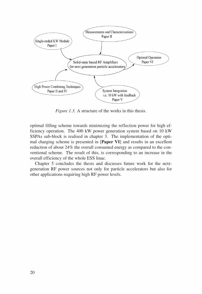
Figure 1.3. A structure of the works in this thesis.
optimal filling scheme towards minimizing the reflection power for high ef-ficiency operation. The 400 kW power generation system based on 10 kWSSPAs sub-block is realised in chapter 3. The implementation of the opti-mal charging scheme is presented in [Paper VI] and results in an excellentreduction of about 24% the overall consumed energy as compared to the con-ventional scheme. The result of this, is corresponding to an increase in theoverall efficiency of the whole ESS linac.
Chapter 5 concludes the thesis and discusses future work for the next-generation RF power sources not only for particle accelerators but also forother applications requiring high RF power levels.
20

2. Accelerators system
2.1 Particle Accelerators BasicsThere are two kinds of radio frequency (RF) particle accelerators mostly inlarge-scale facilities: synchrotrons and linear accelerators. Several large-scaleaccelerator facilities are introduced in Table 2.1. For the synchrotron, the prin-ciple is based on the physical phenomenon that a moving electron emits energywhen it changes direction. An electron gun produces the electrons by applyinghigh voltage through a heated cathode, which is similar to the operating prin-ciple of cathode ray tube in standard televisions [59]. The produced electronsare guided to the linear accelerator (linac) in the form of pulses. The linacaccelerates the electrons to an energy level which is required for injection intoa storage ring. The high energy electrons are transferred from the booster ringto the storage ring, moving in the circumference at nearly the speed of light.As electrons move around the storage ring, they pass a number of magnetsections inside the accelerator ring allowing for the generation of X-rays (thesynchrotron light). The X-ray beams tangent to the storage ring are conveyedinto beamlines where experiments are performed.
Linear accelerator is another type of accelerators where acceleration of thebeam is linear by RF electromagnetic fields and the beam passes the accel-erating sections only once [60]. The concept of RF linear accelerator wasfirst demonstrated experimentally in 1927 [61]. In this paper, an RF volt-age with a peak of 25 kV was applied to a single metal tube between twoground electrodes, producing time-alternating electric field in each gap. Abeam of charged sodium ions, emitted from the cathode, was then acceler-ated and gained with maximum energy when travelling through the gap. Thebeam energy was measured on the order of 50 keV, twice of the gap voltage of25 kV. The experiment established the principle that the voltage gain of an RFaccelerator could exceed the maximum applied voltage [62], since the particlesarrive in gap at the right time to be accelerated. Therefore, the principle couldbe repeated on several drift-tube sections, allowing to achieve higher energiesi.e. [8, 63, 64]. Fig. 2.1 shows a block diagram of a conventional linac struc-ture. Beam of particles is generated by a DC injector system [65,66]. Beam isthen accelerated along a waveguide towards the target. The waveguide struc-ture contains a series of accelerating resonant cavities, which are excited byE-fields created by an external RF power system, see Fig. 2.1. The RF systemprimarily converts DC power provided by a DC power system into RF power.The accelerating structures transfer the electromagnetic energy to the beam,
21

Figure 2.1. A simplified block diagram of a linear structure.
SNS [67] J-PARC [68] ESS ISIS [69] LHC [70]Particle Type H− H− p H− pBeam Current 35 mA 15 μA 62.5 mA 0.25 mA 580 mABeam Energy 1 GeV 30 GeV 2 GeV 800 MeV 7 TeVBeam Power 1 MW 0.75 MW 5 MW 200 kW 200 MW
Table 2.1. A table of existing large accelerator facilities across the world.
allowing for the particles to travel along the linac and help to focus the beamwith support of focusing/steering magnets. Note that the shunt impedance isa valuable figure-of-merit for characterizing the accelerating efficiency of agiven cavity geometry. A vacuum system is provided to make sure that thebeam is not impeded by other particles during the acceleration. The entiresystem is cooled by water i.e. in a normal conducting accelerator, or by liquidhelium i.e. in a superconducting accelerator. The continuous beam comingout of the DC injector system must be grouped into bunches when it enters thesequence of accelerating structures. In order to achieve maximum accelera-tion, the time period between bunches must be a multiple of one or more RFwavelengths.
The linear accelerator offers the capability for reaching high-intensity par-ticle beams and for operating with high repetition pulses or continuous wave(CW), which allows for the acceleration of beams with high average cur-rent [62]. For the linear accelerator, the energy loss is minimized as comparedto the circular accelerator since the beam is accelerated along the straight line.However, the advantage of the high energy comes at the cost of adding accel-erating segments to the length of the linear accelerator, thus increasing its costand maintenance.
RF superconductivity [71] is generating an increasing interest in technol-ogy of choice for future accelerators such as: ESS [8], the X-ray Free Electron
22

Figure 2.2. A layout of ESS linear accelerator.
Laser (XFEL) [72], the Linac Coherent Light Soucre (LCLS) - II [73] , andthe proposed International Linear Collider (ILC) [74]. The use of supercon-ductivity in accelerating cavities brings superior performances for applicationsrequiring CW or long-pulse accelerating fields. This is due to the low Ohmiclosses allowing for a high-field gradient and low power dissipation. This fol-lowing section describes the ESS linac including the linac’s components andsome basic knowledge related to the operation of the linear accelerator with itssuperconducting spokes and elliptical cavities.
2.1.1 The European Spallation Source (ESS) LinacAs can be seen in Fig. 2.2, the ESS linac consists of a proton source, warmconducting sections, cold conducting sections, and a tungsten-based target. Inthe first step, the ion source generates hydrogen ions from heating hydrogengas, which are later stripped of electrons in order to collect the protons. Theformed protons are then guided and accelerated into a 48-meter-long normalconducting (NC) sections. The NC section includes: Low energy beam trans-port (LEBT) section, radio frequency quadrupole (RFQ) section, medium en-ergy beam transport (MEBT) section, and drift tube linac (DTL) section. Allof these sections are operated at a frequency of 352 MHz. The normal con-ducting section provides an energy of 90 MeV to the proton beam. The super-conducting section is followed with 26 spoke cavities operated at 352.21 MHz,60 medium-β and 120 high-β elliptical cavities operated at 704.42 MHz. Atthe end of the ESS linac, a tungsten-based target is bombarded by the protonbeam with an energy of 2 GeV at nearly the speed of light, resulting in thegeneration of neutrons. The following paragraphs cover the details of severalseveral sub-systems and give more insight into the ion source and supercon-ducting sections.
23

Microwave Discharge Ion Source (MDIS):
The microwave-discharge source (MDIS) is placed at the pulsing heart of theESS linac. This is required to produce a proton beam with a high current of62.5 mA. The MDIS system is based on a microwave charge ion source [75]which is widely used for proton production. It uses alternating electric fieldsi.e. at 2.7 GHz to generate a plasma. The ESS proton source design is com-posed of a plasma chamber, an RF generator and RF distribution network,magnetic system, and an extraction system. The RF energy and the hydro-gen gas are injected into a water-cooled, cylindrical plasma chamber througha RF waveguide-based distribution network in which the RF energy is pro-vided to the chamber by using an RF generator at a resonance frequency of2.7 GHz. The magnetic system includes three solenoids providing the axialmagnetic field which allows tuning for matching the injected RF signals andthe hydrogen gas. The ion source, the RF generator and distribution chain,and other components are installed on the high voltage 75 kV platform. Theextraction system is composed of a plasma electrode, two extraction groundelectrodes, and a repeller electrode. The proton beam is expected to achievea beam energy of 75 keV with a maximum emittance of 0.2 π .mm.mrad, dur-ing the 2.86 ms pulse length at 5% duty cycle, and 99.9% reliability definedin [76]. The extracted beam is guided toward the first focusing solenoid of theLEBT.
Low Energy Beam Transport (LEBT):
The LEBT section is the first part of the warm conducting linac, following theextraction system of the ion source. The LEBT consists of two solenoids plustwo correctors, one for the horizontal direction and one for vertical direction.The two solenoids are used for transverse focusing whereas the steerers areused for trajectory corrections. Two devices including an iris and a fast chop-per, allow beam shaping. The LEBT provides the beam matching between theion source and the next section RF quadrupole (RFQ).
Radio Frequency Quadrupole (RFQ):
The RFQ section takes charge of accelerating the extracted proton beamfrom the ion source, transversely focusing it, and longitudinally bunchingit in providing the performance of acceleration in the further stages of thelinac.The RFQ is based on a 4-vane structure resonating in the TE210 mode at352.21 MHz. It is divided into 5 sections for a total length of 4.6 m. The beamenergies at the output of the RFQ are on the order of a few MeV (i.e. for ESSRFQ the beam energy is 3.6 MeV). More details can be found in [77].
Medium Energy Beam Transport (MEBT):
The MEBT section acts as a steering and matching section between the up-stream RFQ and the adjacent section DTL. It has 11 magnets, 3 buncher cavi-ties, 1 fast chopper, 1 beam dump, 2 beam scrappers, and a set of beam instru-
24

mentation for diagnostics. The length of this section is on the order of 4 m.The use of the scrappers allows to remove the pulse head/tail during the tran-sient times of the ion source and the LEBT, improves the beam quality as wellas the beam losses due to the partially-chopped bunches [78].
Drift Tube Linac (DTL):
The drift-tube section is located in the last stage of the warm conducting partof the linac. It is made by 5 tanks with 173 drift tubes, which are equipped withbeam position monitor (BPM), electromagnetic dipole (EDM) , and permanentquadrupole magnet (PMQ) [79]. Each of the tanks requires a power generationof 2.2 kW to increase an energy for a proton beam current of 62.5 mA from3.6 MeV to 90 MeV. The DTL is designed to operate at 352 MHz with a dutycycle of 4% and 2.86 ms pulse length.
Spoke cavities:
The superconducting linac starts with the spoke section, which will acceleratethe proton beam extracted from the DTL section from 90 MeV up to 216 MeV.The spoke section has a total of 26 cavities for a total of 56 m in length.The spoke cavities are made of Niobium, designed to be matched at relativebeam velocity of β = 0.5. Two spoke cavities are paired in a cryomodule andare immersed in helium liquid at 2K since Niobium becomes superconductorwhen cooled below 9K. The SRF spoke cavities require an accelerating fieldof 9 V/m, which is realizable by using an average power of 250 kW per cavity.Insights of design and testing can be found in [80, 81].
Medium-β and High-β sections:
The spoke section is followed by the accelerating structures, consisting of60 medium-β and 120 high-β elliptical cavities. Those cavities occupy thelongest portion of the ESS linac (about 256 m in length). In this section, ac-celeration is performed at the resonating frequency of 704.42 MHz with anenergy transition at 571 MeV until the proton beam reaches 2 GeV at gradi-ent of 18 MV/m, prior to the HEBT section [82]. Testing performance of thesection can be found in [83].
High Energy Beam Transport (HEBT):
After acceleration up to 2 GeV, the proton beam is transported from the linactunnel to the target which is 4 m higher at the surface level. The HEBT sec-tion inclues: a 128-m upgrade high-β (UHB) sub-section, a 69-m-long dog-leg, acceleration to target with total length of 45 m, and a beam dump linesub-section [84]. The UHB sub-section provides space for extended cryomod-ules if upgrades in the future are made, and for contingency purposes. Then,the achromatic dogleg is to steer the proton beam 4 m up to the target level.The last sub-section is to transport the beam to the target using a set of 6quadrupoles and 8 raster magnets. More details are given in [84].
25

Tungsten Target Station:
At the target section, the spallation process is performed, resulting in the pro-duction of high-intensity neutron beams. The more neutrons are produced inthe collision of the spallation process, the brighter the neutron source is. ESSwill be 100 times brighter than any of the existing spallation sources. Thetarget is made of tungsten, divided into 33 sectors with 2.5 m in diameter.Proton beam pulses are synchronized with the rotation speed of the target at25 rpm. The high-energy spallation neutrons are transformed into slow neu-trons at the speed of sound by using the moderator-reflector assembly carefullysurrounding the target [85]. A radiation shielding system of 7000 tons of steelis surrounded the target and allows to prevent unwanted radiation from leak-ing. The beam extraction system provides the neutron beams via beam guideslocated in arcs around the station. These slow neutron beams are accessibleat the surface of the station to spectrometers, allowing scientists to carry outtheir experiments.
2.1.2 Some basic definitionsThis section covers insightful explanations of the basic terms and definitionswhich are commonly used in particle accelerators.
Acceleration and focusing:
The acceleration/bending/focusing processes are described by the Lorentzforce, as the total force on a charged particle moving through both an elec-tric field and a magnetic field:
d�pdt
= q(�E +�v�B) (2.1)
in which �p is the particle momentum,�v is the velocity, q is the electric charge.Particles are accelerated by electric fields, whereas they are focused and bentby magnetic fields (i.e. quadrupole focusing with 4-poles magnets).
Particle velocity and energy:
Particles are divided into light particles and heavy particles. The light par-ticles (i.e. electrons) reach a constant velocity at relatively low energy. Theacceleration process occurs at constant particle velocity. Heavy particles (i.eprotons and neutrons) reach a constant velocity at high energy. The velocitychanges along the linac during the acceleration process. ESS proton linac hasa number of accelerating structures, each optimized in geometry and energyfor accelerating the proton beam to a high energy of 2 GeV.
Electrostatic acceleration:
The principle of electrostatic acceleration was used for the first time in theCockcroft-Walton accelerator [86]. If a particle travels through an electric
26

Figure 2.3. A picture of RF acceleration in time.
Figure 2.4. A schematic of resonant cavity with a RF generator, a coupler, and highpower transmission lines.
field generated by a potential V, it will gain a kinetic energy:
ΔE = q× e×V (2.2)
in which 1 eV is the energy of an electron accelerated under a potential of 1 V.Electrostatic acceleration is often used at the sources section of accelerator.
RF acceleration:
The electrostatic accelerator is limited in accelerated energy since it requirespractical potential difference. The particle is passed through an RF field whichis provided by a RF generator. This concept was first used in the accelerationof particles of higher energy, with low gap voltage [61]. The accelerating elec-trodes must be arranged such that the accelerating field changes as the particlepasses at the right point. This is also a conventional method of producingbunched beam [87], see Fig. 2.3.
RF accelerating cavities:
The acceleration technique presented in [61] requires the relativistic factorβ << 1, thus it is unable to apply for relativistic particles. The relativistic
27

factor β is defined as the ratio between the velocity of a moving particle andthe speed of light. As particles get high velocities, the energy gain per unitlength decreases, resulting in a longer drift spaces in order to deliver higheraccelerating gradient. Therefore, a design of high frequency is needed al-lowing a required increase in the accelerating gradient. To do so, a popularscheme in particle accelerators is to have a series of resonant cavities in whichthe resonant frequency matches the RF generator frequency. The RF cavityis a metallic chamber that confines an electric field in the form of the cavitymodes. For almost all RF cavities, the T M010 accelerating mode is preferablyused since it has a longitudinal electric field, therefore it accelerates particlesin the direction of propagation. The modes of the cavities can be excited by RFgenerators coupled to cavities using waveguides, capacitive/inductive coaxialcables, etc. Resonant modes of EM waves in a cavity can be represented by aequivalent resonant R-L-C circuit, in Fig. 2.4. The equivalent circuit is used al-lowing for analyzing the build-up of electric fields as the result of a reflectionof waves inside the cavity during the charging time, see [Paper VI]. Cavitiescan be made of normal conducting or superconducting materials depending onrequirements of accelerating gradient, pulse length, duty cycle, average beamcurrent, etc. Multi-cell structure is an array of accelerating single cavities withonly one RF input coupler, thus reducing the number of RF sources [88].
Principle of phase stability:
As mentioned in previous sections, energy gain of the particles travelling alongthe accelerating cavities depends on the arrival time of the particles (or arrivalphase φS). The accelerated particles in the linac remain to be synchronizedwith the accelerating fields, called synchronous particle with a synchronousphase on the positive slope of the RF voltage see Fig. 2.5. The particles thatarrive earlier than the synchronous phase point (black dot) will gain less energywhereas the particles coming at late phase will experience higher energy. Thisprovides longitudinal focusing of the beam in which a longitudinal restoring
Figure 2.5. Energy gained by a particle as a function of arrival time.
28

force exists when the synchronous phase is chosen corresponding to a time-varying field [62]. Forces keep the beam oscillating about the synchronousphase, providing phase stability. For ESS baseline design, phase stability isone of stringent requirements. This is specified to be 0.1o [8].
2.2 Review of power generation sources for particleaccelerators
In this section, a review of technologies for power generation systems to beused in particle accelerators is introduced. The review covers a broad rangeof established technologies including: Tetrode amplifiers, Inductive OutputTubes (IoTs), Klystron amplifiers.
2.2.1 Tetrode-based amplifiersTetrode vacuum tubes are established in the frequency band ranging from30 MHz to 400 MHz. The output power is technically dependent on the max-imum current density from the cathode and the maximum power density dis-sipated by the anode [89]. Similar to a conventional grid tube, the TetrodeTH595 has 4 active- electrodes, including: a filament, a control grid, a screengrid and an anode plate. They are arranged in coaxial structure in which thecathode is inside and the insulated anode is outside, see Fig. 2.6. The spac-ings between electrodes must be small enough to allow the short transit timeof electrons from cathode to anode. Each of the electrodes is connected to asingle power supply. For the 400 kW tetrode-based amplifier at FREIA, twotetrode (TH595) from Thales are used, each delivering 200 kW peak power inpulsed mode. A single anode power supply from Astron Electronic AG is usedto provide DC voltage of 16 kW for two tetrode amplifiers combined with abank of capacitors, crowbar unit for protection, high voltage limiters, and fil-ters [90]. The disadvantage of this configuration is that once arcing happensat one amplifier, this could lead to a damage to the other amplifier. The highvoltage anode power supply is quite bulky and accounts for 3 racks 5U-19-inchplus room occupied by the high voltage capacitor in the system [91]. For thefilament power supply, an AC voltage single phase supply is used to ramp thevoltage from 0V to 8V for the filament. It takes 10 minutes for the warm-upoperation. For the control grid power supply, it generates negative voltage of-173 V with respect to the cathode for a class AB operation. The screen grid isused for suppressing the Miller effect, thus avoiding instability at high frequen-cies. The power supply for the screen grid is maintained constant at 900 V, farbelow the anode voltage. Along with the water-cooled and air-cooled system,each of tetrode amplifiers accounts for 25% of the power station’s space.
The available gain of the TH595 is on the order of 12 dB. Therefore, a10 kW driver stage is required in oder to deliver an output peak power of
29

(a)
(b)Figure 2.6. A picture of Tetrode-based amplifier in the power station installed atFREIA. (a) Tetrode TH595, (b) Tetrode cavity TH18595.
200 kW. Yet another requirement of space for the tetrode-based station whendelivering higher output power is that a bulky combiner is necessary i.e. a3-dB hybrid combiner is located on the top of the station for combining 2outputs from tetrode amplifiers into a total of 400 kW output power. Usingsuch hybrid combiners results in an addition of high power loads (i.e. 200 kWat the load arm of the combiner). For such configuration, the loads should becapable of handling high power if one tube fails and isolate the other one. Theanode efficiency of the system is measured on the order of 60% at the nominalmax output power of 200 kW [91] under ESS pulsed condition [8].
2.2.2 Inductive output tube amplifiersFor tetrode amplifiers, the output power is limited due to the power dissipationwithin a small volume [89]. Such constraint can be overcome by isolatingthe electron beam and the RF output circuit, see Fig. 2.7. This was firstlydemonstrated by Haeff in his invention called "Inductive Output Tube" [92].In an IOT amplifier, major components include: electron gun, anode, inputcavity, output cavity, collector, see Fig. 2.7. An electron gun is used to emitelectrons, which then are accelerated towards the collector. An RF signal isapplied to the gap between the grid electrode and the cathode. The grid isbased at a negative DC voltage (i.e. similar to a class-B operation). Thisallows the formation of electron bunches. The bunches are accelerated by theelectric fields between the anode and cathode. The bunches excite resonantfields at the output re-entrant-based cavity and the magnetic field induces acurrent in the cavity. The output power is then extracted via an inductivelycoupled coaxial line.
30

Figure 2.7. The architecture of a conventional IOT amplifier. Reprinted with permis-sion from [93]. Copyright IEEE 2009.
IOTs generates their output power from the modulation of the beam viathe output cavity. Therefore, the output power can be increased as high asthe beam voltage, resulting in a high conversion efficiency in the range from70% to 80%. For IOTs, the output and input are completely isolated, thusthe input and output are easily tuned. The lifetime of IOTs is reported tobe over 40000 hours as compared to 20000 hours for tetrode amplifiers [94].Mutli-beam IOT is demonstrated [36] with 1.2 MW output power at 704 MHzand is a potential candidate to replace the Klystron technology for ESS high-β cavities. However, this technology is still under development and somechallenges should be taken into consideration. The limit of the beam voltagedue to the voltage breakdown in vacuum practically results in a boundary of theoutput power for this technology (i.e. 100 kW output power for a single IOT).Due to a large potential between anode electrode (more than 27 kV of appliedvoltage) and cathode electrode, arcing might happen causing the deteriorationof performance, thus reducing the lifetime of the tube.
2.2.3 Klystron amplifiersTo date, Klystron is the technology of choice in particle accelerators when re-quiring extremely high power (i.e. in the range of MW) and high frequency(i.e. up to GHz). Klystron amplifiers work on the principle of velocity mod-ulation. An electron gun produces a stream of electrons travelling at samespeed. The electron beam then passes through a pair of spaced grids, whichis called buncher grids. The buncher grids are connected to a resonant cavityproducing an electric field between them. The electric field alternately accel-
31

Figure 2.8. The architecture of a conventional Klystron amplifier. Reprinted withpermission from [97]. Copyright Research Study Press (1994).
erates and decelerates the electron beam passing the section, forming bunchesof electrons. The buncher grids are followed by the catcher grids. The RF cur-rent carried by the beam produces an RF magnetic field, which then excitesby using the second catcher cavity. The position of the cavity is determinedby the transit time of the bunches at the same frequency of the buncher andcatcher cavities, thus allowing for maximally transferring energy to the out-put. The number of cavities can be more than two allowing for an increasedgain or bandwidth. For ESS elliptical cavities [8], Klystron amplifiers fromToshia are used allowing for 1.5 MW peak power at 704 MHz in pulsed modeat a repetition frequency of 14 Hz. A high power modulator [95] is needed tooperate the Klystron. Insights of test stand and results can be found in [96].
32

3. Results
The working principle of the solid-state based power system is determined byboth how the individual modules are operated and how the outputs are com-bined. The choice of system architecture depends on the demand of outputpower, transistor technology, and combining method, see Fig. 3.1. This chap-ter gives the insights needed to understand and design the system from ampli-fier modules to combiners. The know-how to integrate individual componentsfor scaling up the output power is also discussed. In this chapter, the systemdesign approach starts with a discussion about the single-ended architectureat the kilowatt module. It is shown that the feasibility of single-ended con-figuration allows for high efficiency, simple architecture for mass production[Paper I] as compared to other major configurations i.e. the push-pull config-uration [98]. Since ESS SC cavities require high peak power i.e. 400 kW forESS spoke cavities, thus a few hundreds of kW modules are needed. The sim-plicity of the single-ended architecture facilitates the fabrication and the tuningprocedure when combining them. The validation of the single-ended solutionapplied to a PA design is characterized in time domain to make sure that itmeets the stringent demands for amplitude and phase at kilowatt level [Paper
II]. This chapter shows also engineering solutions of combiners based on con-
Figure 3.1. A conventional block diagram of N-way power amplifier system with Nnumber of power amplifier modules and divider/combiner.
33

ventional Gysel topology [Paper III] and re-entrant cavity structure [Paper
IV]. All combiners satisfy the requirements of low loss and high power. Forthe Gysel-based combiner, it was demonstrated to operate with low loss at10 kW [99], 20 kW power level [Paper III]. The reentrant-cavity combineris tested at a power level of few hundreds kW. This chapter provides insightsof the integration process in which each of stages is designed and fine-tunedfollowing a specific procedure to achieve the objectives of performance i.e.output power, stability, linearity, amplitude and phase imbalance, etc. Each ofthe single modules in the system is tuned in a systematic way to achieve thebest combining efficiency regarding amplitude and phase [Paper V].
3.1 High efficiency LDMOS-based power amplifiersPush-pull circuit configuration has been widely used [100,101] since it allowsfor the realization of wide-band power amplifiers [102–104] usually combinedwith an ultra-wide-band balun [105], high output power [106–111], and en-hanced even-order harmonic suppression [112, 113]. The push-pull configu-ration uses a pair of similar transistors, connected through a balun (balanced-unbalanced) transformer at both input and output. The two devices are biasedin deep class AB mode [114–117]. The key benefits of push pull configurationare reduced common lead effects and impedance benefit for easy in/out match-ing [118]. However, the requirements of balance among branches in baluns ischallenging, since any imbalance reflects back to the transistors, i.e. amplitudedifference among input signals to each of branches or among unequal loads tothe transistors. The design of power stations for particle accelerators, baluns(i.e. coaxial type) seems not to be practically suitable when a few hundreds ofpower amplifier modules are needed. The push pull configuration was not
chosen for the solid-state based system in this thesis. Instead, the require-ments from ESS i.e. the extremely narrow bandwidth [8] justifies the use ofthe single-ended configuration [Paper I] with the specifications for EuropeanSpallation Source (ESS) at 352 MHz in pulsed mode with a duty cycle of 5%.In addition, the distributed design approach for single-ended amplifiers bringsa range of advantages, i.e. simplicity in design without a need of baluns, suit-able for mass production to build up 400 kW stations [119], and representsan economical design. It was demonstrated that the single-ended amplifier[Paper I] can deliver output power in the kilowatt level with superior perfor-mance in efficiency thanks to the choice of transistors and harmonics suppres-sion of the developed resonant matching technique.
3.1.1 Realization of single-ended design at kilowatt levelThe solid state power amplifier (SSPA) module was built around the LDMOSBLF188XR transistor, see in Fig. 3.2. Efficiency and output power are thetwo most important design constraints imposed on the design approach. In the
34
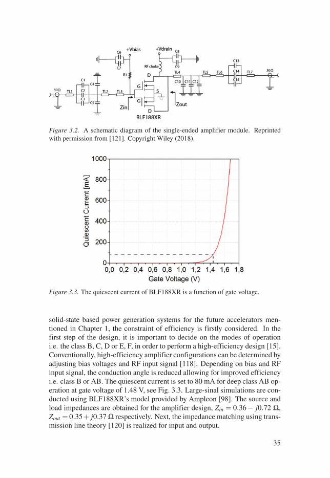
Figure 3.2. A schematic diagram of the single-ended amplifier module. Reprintedwith permission from [121]. Copyright Wiley (2018).
Figure 3.3. The quiescent current of BLF188XR is a function of gate voltage.
solid-state based power generation systems for the future accelerators men-tioned in Chapter 1, the constraint of efficiency is firstly considered. In thefirst step of the design, it is important to decide on the modes of operationi.e. the class B, C, D or E, F, in order to perform a high-efficiency design [15].Conventionally, high-efficiency amplifier configurations can be determined byadjusting bias voltages and RF input signal [118]. Depending on bias and RFinput signal, the conduction angle is reduced allowing for improved efficiencyi.e. class B or AB. The quiescent current is set to 80 mA for deep class AB op-eration at gate voltage of 1.48 V, see Fig. 3.3. Large-sinal simulations are con-ducted using BLF188XR’s model provided by Ampleon [98]. The source andload impedances are obtained for the amplifier design, Zin = 0.36− j0.72 Ω,Zout = 0.35+ j0.37 Ω respectively. Next, the impedance matching using trans-mission line theory [120] is realized for input and output.
35

Figure 3.4. Layout of the SIR structure with one end terminated ZL.
Both input matching and output matching networks are based on stepped-impedance resonator (SIR) structure [122–127] at frequency of interest352 MHz ± 2 MHz. In the design approach, SIR structures are formedby a cascade of two-stepped transmission lines with different characteristicimpedance. Fig. 3.4 shows the SIR structure with one end connected to loadZL. The input impedance seen from the open-end of the structure is denotedas Zin. The input admittance can then be derived as following:
Yin =1
Zin= Y2
Z1Z2 + jZ2ZL tanθ1 + jZ1ZL tanθ2−Z21 tanθ1 tanθ2
Z1ZL + jZ21 tanθ1 + jZ1Z2 tanθ2−Z2ZL tanθ1 tanθ2
(3.1)
in which θ1andθ2 are the electrical length of transmission line sections. Theparallel resonance occurs when Yin = 0. The resonance condition can be writ-ten as:
Z1Z2 + jZ2ZL tanθ1 + jZ1ZL tanθ2−Z21 tanθ1 tanθ2 = 0 (3.2)
or,Z1(Z2−Z1 tanθ1 tanθ2)+ jZL(Z2 tanθ1 + jZ1 tanθ2) = 0 (3.3)
K is defined as the electrical length ratio of the resonator:
θ1 = KθT (3.4)
θ2 = (1−K)θT (3.5)
, in which θT is the overall electrical length of the resonator. The Eq. 3.3 canbe re-written as:
Z2(Z1 + jZL tan(KθT ))+ jZ1(ZL + jZ1 tan(KθT )) tan(1−K)θT = 0 (3.6)
Numerical simulations are performed for the input and output resonantmatching networks using Keysight Advanced Design System (ADS). For the
36

Figure 3.5. Characteristic of harmonic filtering as a function of frequency at the outputmatching network.
nominal power PL = 1250 W , the simulated input and output impedances areclose to the short-circuit. These matching networks at input and output arebased on SIR structure and act as band-pass filters at the resonant frequencyof 352 MHz allowing for enhancing attenuation of the second and third har-monics. In this design approach, the harmonic filtering shapes waveforms atthe drain towards i.e. class F [15]. The simulated results of harmonic filter-ing are shown in Fig. 3.5. At the output port of the amplifier [Paper I], thesecond harmonic and third harmonic levels are obtained -17 dB and -15 dBrespectively.
Figure 3.6. The return loss versus frequency is simulated at the input and output.
37

Figure 3.7. Characteristic of harmonic filtering as a function of frequency at the inputmatching network.
(a) (b)Figure 3.8. Gain and efficiency simulation results are as a function of output power.Adapted with permission from [128]. Copyright (2016) IET.
For the input matching port of the amplifier, second harmonic level is simu-lated as better as -25 dB, while the third harmonic level is -15 dB. Large-signalharmonic balance is then performed with BLF188XR model using ADS [129].Harmonic balance solver allow for validating the full amplifier with input andoutput matching networks as simulated in Fig. 3.5 and Fig. 3.7. A capacitoris added close to the drain of the transistor for improving the matching condi-tions of resonance. The optimal value of the capacitor is 27 pF and was splittedinto 3 smaller capacitors (C10,C11,C12) to avoid overheating, which is causedby high current i.e. 35 A at kilowatt output power, see Fig. 3.2. Efficiencyand output power can be slightly tuned by moving those capacitors furtherfrom or towards the transistor. For a large number of similar modules, thisfine tuning process can be used to compensate the variation among active de-vices, allowing for improved combining efficiency. In this high power design,
38

Figure 3.9. A picture of the prototype amplifier manufactured in RO3003. Adaptedwith permission from [128]. Copyright (2016) IET.
several coupling capacitors are used at the input (C1,C2,C3) and the output(C13,C14,C15). Details of the design considerations can be found in [Paper
I]. The simulated characteristics of the gain and the efficiency are obtained,see in Fig. 3.8. The simulated efficiency is on the order of 73% as delivering1.25 kW output power at 5% duty cycle.
The design is realized on RO3003 substrate with εr = 3, tanδ = 0.001, cop-per thickness = 35 μm, substrate thickness = 76 μm. All of the microwave ca-pacitors are chosen from American Technical Ceramics 800B’s series, whichoffer low equivalent series resistance (ESR), very good heat transfer for highpower applications. The heat is dissipated through an aluminum base plate.The base plate is provided with a tube of 10 mm in diameter. Water-coolingis located 10 mm under the transistor flange, see Fig. 3.9. One should notethat if there is a drop of more than 5% in power over a short period of time, itis probably due to overheating. The cooling system might be improved [130],allowing for better thermal transfer from heat sources to heat-sink.
The characterization is performed in both frequency and time domain. Inthe frequency domain, hot S-parameter measurements [131–133] are imple-mented allowing for fine-tuning matching networks at high power level, i.e.above 1 kW. Fig. 3.10 introduces a block diagram of hot S-parameter setup atkilowatt power level. Details can be found in [119] regarding the measurementsetup and results. For the RF power generation systems to be used at ESS,the requirements of amplitude and phase variations are stringent i.e. 0.1% inamplitude and 0.5% in phase [8]. To validate the design in [Paper I], time-domain characterization is implemented with a measurement setup [Paper II]developed for high power level. The integration of SSPA-based system willbenefit from time-domain measurements i.e. evaluating any imbalances inamplitude and phase among individual modules in order to achieve the bestperformance in combining efficiency. In the following sub-chapter, the timedomain characterization and measurement results will be presented.
39

Figure 3.10. A picture of block diagram of hot S-parameter setup. Reprinted withpermission from [119]. Copyright (2014) JACoW .
Figure 3.11. An example of pulse profile in time domain.
3.2 High power time-domain characterizationThe energy use for accelerating the particles should be constant during thepulse of 3.5 ms. The particle accelerator, i.e. superconducting cavities, mustestablish a stable accelerating voltage to supply the same energy. The sta-ble accelerating voltage needs from the RF power station with a stability per-formance in amplitude of 0.1% and phase of 0.5o [8]. Concerns about suchpower generation system include pulse drop, variations during the flat-top ofthe pulse, pulse-to-pulse stability, rise time, fall time, see Fig. 3.11. Theseconstraints are of paramount importance when using solid state amplifiers asa power generation system. One issue about solid-state based power ampli-fiers is that they exhibit pulse drop in which the amplitude of a pulse trailsoff over time [117, 134–138] as delivering high peak output power, i.e. kWoutput range. This causes instability in particle accelerators when the beam is
40

Figure 3.12. A picture of RF pulse profile measurement setup. Adapted with permis-sion from [121]. Copyright (2018) Wiley.
injected with inconsistent experienced energy during the pulse. Another causeof instability considered is the risk of pulse-to-pulse (P2P) stability. P2P insta-bility is characterized by variations of envelope amplitude and phase over timefor successive RF pulses. For system level characterization, P2P stability isnormally characterized at the very final step of the design process. This leadsto insufficient knowledge on the limitations for the power amplifier module re-garding amplitude and phase noise. This sub-chapter presents the developmentof a time-domain characterization methodology for high power SSPA module[Paper I] operated in pulsed mode. The non-linear time-domain simulationsat the circuit level allow to gain an early insight into the design matching so-lutions and identify actual causes of instabilities. Such instabilities are dueto over-heating or pulse-to-pulse random variations, and transistor technolo-gies [139]. The time-domain characterized results are then be used by thelow level RF (LLRF) controller [140] as priori knowledge for implementingthe suitable control strategies, i.e. strategy for the compensation of the powerdroop compensation, see [Paper V].
3.2.1 Measurement setupIn [Paper II], the block diagram of the time domain characterization setupis presented, see Fig. 3.12. The measurement setup is well-suited for highpower levels ranging from few hundreds of W to kW. Two receiver architec-tures are used for the realization of the time-domain measurement setup in-cluding zero-IF [141–143] and heterodyne [139, 144, 145] architecture. The
41

setup in [Paper II] is based on heterodyne architecture in which the local os-cillator (LO) can be tuned to bring the input frequency range into intermediatefrequency (IF) for extracting desired information. After mixing, the image fre-quency is suppressed by a low-pass filter, allowing to meet the image rejectionrequirements. An additional mixing is implemented to extract the I (In-phase)and Q (Quadrature) signals. The extracted data is captured and analyzed via aMatlab-based platform to realize the characterization of the pulse profile. Theheterodyne technique offers a wide range of advantages including DC-offsetcancellation, an extent relaxation of I-Q mismatch, good sensitivity. These arethe main reasons why the heterodyne architecture is used for measuring time-domain performance of the SSPA module [Paper I]. In the heterodyne setup[Paper II], the RTO1024 oscilloscope is used as heterodyne receiver [146].Details of measurement setup can be found in [Paper II].
For time-domain characterization, the acquisition of N pulses is realizedat sample rate of 500 kS/s after the mixer stage with the support of softwareRTO-K11. The corresponding IQ data at 500 KS/s is then exported to Matlabto be analyzed. The transmission lines (πmeasure2 and πout ; πmeasure1,and πin)are connected together by passive networks consisting of high power couplers,attenuators, power splitters, and RF cables, see Fig. 3.12. The calibrationprocedure is described as following:• Step 1: To capture voltage waveforms at SSPA input and output reference
planes, normalization must be performed to take into account for offsetcoefficients depending on the passive networks. A commercial vectornetwork analyzer (N5221A) performs S-parameter measurements of thetwo-port passive networks. From these measurements, the offset coeffi-cients are derived and used to correct values at (πin, πout). In this step, itis assumed that couplers offer high directivity and negligible mismatchuncertainty among individual components.
• Step 2: The phase offset between πmeasure1 and πmeasure2 is characterizedwith a through transmission between πin and πout from extracted IQ data.
• Step 3: Two power meters (N1912A) measure the average envelopepower at the πin input and πout output planes as power calibration ref-erences.
• Step 4: A Matlab-based script executes the measurements of envelopeamplitude and phase by extracting the IQ data and correcting with cali-brated data from Step 1 to Step 3. Then, P2P stability normalization andcalculations can be realized.
3.2.2 Simulation and measurement results discussionThe non-linear simulations are based on the circuit envelope (CE) method de-scribed in [147, 148]. In the CE method, the input waveforms are representedas RF carrier in frequency domain, with modulation envelopes in time do-
42

Figure 3.13. A modulated RF signal with its simulated time-varying spectrum in step-by-step simulation process. Adapted with permission from [149].
main. The CE method is a combination of harmonic balance and time-domainsimulation techniques, see Fig. 3.13. First, a time-domain analysis is realizedto sample the modulation envelope. Then at each time sample the circuit en-velope simulator performs harmonic balance to compute a time-varying spec-trum. Therefore, the method offers a greatly reduced computation for completeanalysis of the modulated RF signals and P2P stability.
The simulated results are compared with the measured results in time do-main for a single pulse. The design in [Paper I] includes an energy storagecapacitor. This allows avoiding using a big power supply [138]. For the pulsedRF system in Fig. 3.1, the storage capacitors in a capacitor bank accumulatethe energy during the silence of the pulse. The accumulated energy is thenprovided for amplification [Paper I] during the pulse. This leads to a verycompact design solution for the system. As demonstrated in [Paper II], thedesign in [Paper I] exhibits a voltage droop due to the storage capacitor dis-charge. The voltage droop is caused by the equivalent series resistance (ESR)of the capacitor and the capacitor discharge. The energy storage capacitanceis chosen as follows:
C =IxdtdV
(3.7)
, where I = peak current, dt = pulse length, dV = pulse voltage drop.Fig. 3.14 shows the measured voltage drop when the SSPA module delivers
1.25 kW output power. The drop is measured on the order of 1 V at the endof the pulse of 3.5 ms. Due to the voltage droop, it is observed that there is adroop of 0.2 dB corresponding to 4% reduction in amplitude. The measureddrop agrees well with the simulation results, see Fig. 3.15. This leads also toa drop of the insertion phase, which can be found in [121]. The use of storagecapacitors is unavoidable in pulsed RF power amplifiers. For pulsed particleaccelerator systems, the inherent drop results in the charged particles’ instabil-ities during acceleration. A control strategy is adopted using LLRF controllerallowing for compensating the inherent drop. The details regarding the LLRF
43

Figure 3.14. Measured result of drain voltage at 1.25 kW output power. Adapted withpermission from [Paper II] [121].
Figure 3.15. A drop of amplitude within the pulse in time domain at 1.25 kW outputpower. Reprinted with permission from [Paper II] [121]. Copyright (2018) Wiley.
controller and implementation of the control strategy will be discussed in sec-tion 3.4. The lifespan of storage capacitors is degraded due to current ripple,over-heating caused by the ESR, applied voltages beyond the rated voltage ofthe capacitors, etc. Therefore, it is important to consider all of the factors thatcan accelerate the failure rate of the storage capacitors in the pulsed powergeneration systems for particle accelerators. In the section 3.4, some practicalconsiderations regarding selection of storage capacitors will be discussed.
As mentioned, P2P stability is of prime importance in power generation sys-tems. Power amplifiers might adversely affect stability. Therefore, precise sta-bility measurements of such amplifiers is paramount in order to maximize theoverall stability of the whole system. The P2P stability is calculated by usinga regular and repetitive sequence of the pulse-modulated RF carrier with iden-
44

Figure 3.16. The envelope diagram of the RF pulsed signal with arbitrary pulse width(PW) and repetition rate period (PRP). Reprinted with permission from [Paper II][121].Copyright (2018) Wiley.
(a) (b)Figure 3.17. Measured results of amplitude and phase stability using time-domainenvelope measurement [Paper II]. Reprinted with permission from [121]. Copyright(2018) Wiley.
tical pulse widths and identical pulse repetition periods of the envelope [139].In this thesis, the P2P stability is characterized by using the time-domain enve-lope measurement setup [Paper II]. From envelope diagram of the RF pulsedsignal in Fig. 3.16, the values for the stability can be given as follows:
Stab(tk) = 10× log
[1N
N
∑i=1
(Vout_i(tk)−Vout(tk)
)2
](3.8)
Vout(tk) =1N
N
∑i=1
Vout_i(tk) (3.9)
where the index i refers to the ith pulse in the sequence. The value Vout_ican be either amplitude or phase at sampling points of given N pulses in
45

case of amplitude stability or phase stability measurements. In this thesis,the time-domain envelope measurements of amplitude and phase P2P stabilityare performed under periodic RF pulses without silence. The P2P stability inamplitude and phase are obtained on the order of -80 dB and -24 dB. This isbecause non-linear distortions (thermal effects) are similar from pulse to pulse,see Fig. 3.17. In addition to stability measurements, simulations on amplitudeand phase stability are performed by using circuit envelope method. To evalu-ate how attributable the design [Paper I] is on overall stability, an input signalis applied with uniform distribution of amplitude. Then the envelope simula-tor runs Monte Carlo analysis to obtain P2P variability in amplitude and phaseat the output, see Fig. 3.17. The simulated results match well to the measuredresults at 1.25 kW output power. By using the envelope simulation presentedin [Paper II], it is possible to use the non-linear model for the transistor inorder to predict P2P stability performances. This allows for early insights onacceptable levels of amplitude and phase on critical components such as poweramplifiers, which specifies by the tolerance of amplitude and phase of particleaccelerators, i.e. for ESS requirements of 0.1% in amplitude and 0.5o in phase.The achieved results give the upper limits for the LLRF controller, to regulateits amplitude and phase errors.
3.3 High power combiner approachAs can be seen in the combining architecture described in Fig. 3.1, the low-power amplifier modules are combined in a way to achieve the output powerlevels with the best efficiency performance. For solid-state based power gener-ation systems, the system efficiency is determined by the mismatch in ampli-tude and phase among power amplifier modules, loss of the combiner, numberof failure modules, output matching of the combiner, and number of combin-ing modules [58, 150–152]. The mismatch among amplifier modules will bediscussed in the section 3.4. This section presents several engineering solu-tions [Paper III and Paper IV] allowing for the realization of the power sum-mation of individual PA modules with improved efficiency and high powerhandling capability. Power combiners are mostly based on quarter-wavelengthstructure such as: Wilkinson [153], Gysel [154], coupled-line [155], rat-racering [156], etc. The combining stage might include single or multiple stagesfrom low power to high power, see Fig. 3.18. The combiner is designed in pla-nar technology [99, 157] or is waveguide-based structure [158–160], depend-ing on the demand and power-handling levels. In this thesis, two engineeringsolutions are adopted for power summation of individual modules. The firstdesign [Paper III] is based on a conventional Gysel configuration using shieldstrip-lines in order to improve the power handling capability. The other [Paper
IV] combiner design uses re-entrant cavity structure, with 12 inputs.
46

Figure 3.18. A picture of combining architecture for a conceptual design of solid-state 400-kW system. The combining stage consists of 3 stages including Gysel-typecombiner for 10 kW level, cavity-based combiner for 100 kW level, and waveguide-based combiner for 400 kW level. Reprinted with permission from [Paper VI].
3.3.1 Low and mid range power combining solutionFor high power applications, Gysel-based structure [154] has widely beenused. The Gysel type structure offers the use of external isolation loads,monitoring capability of tolerances among input ports, and is an easy-to-implement geometry. The use of external high-power isolating loads makes theGysel-based structure far better in comparison to the Wilkinson structure. Astacked arrangement, implemented on planar technology, leads to a very com-pact assembly at very high frequency (VHF) or ultra high frequency (UHF)range [99, 161]. However, it can be demonstrated that such Gysel combiner isnot suitable for a large number of inputs, i.e. more than 10 inputs due to thefloating common star point. This explains why Gysel is chosen in this thesisfor combining a sub-block of 8 inputs allowing to achieve 10 kW output power[Paper V]. For higher power levels, the cavity and radial design approach arepreferred [158,160, 162–164] due to the availability of more inputs.
In Paper III, a Gysel-based combiner is adopted employing shielded strip-line techniques [165–167] with an air gap above and below the strip-line. Thepower handling capability of this configuration depends on the breakdownvoltage of strip-lines and connectors. As can be seen in Fig. 3.19b, the spacingbetween copper traces (in yellow) and ground planes (lower and upper plates)are supported and held by fixed spacers. The traces are in conjunction withassociated ground planes and define the suspended striplines. This allows forhigh power operation with inherent ventilation capability. For shielded strip-lines, the impedance can be optimized by adjusting the width of the tracesand the spacing between the strip-lines and ground planes. In the assembly,spacing is 17.5 mm, the thickness of copper plates is 1.5 mm to handle the
47

(a) (b)
Figure 3.19. (a) The fabricated Gysel-based combiner. (b) A cross section of thestrip-line structure with the mechanical tuner above and below the strip metal traces.[Paper III]. Reprinted with permission from [170]. Copyright (2018) IET.
temperature rise of strip conductor at high power levels [168]. The width ofcharacteristic impedance is then deduced using Cohn’s approximation [169]as following:
Z =94.15
√εr
(W/H
1−t/H +C′f
0.0885εr
)Ω (3.10)
where C′f is the fringing capacitance in μF per centimetre, which is eval-uated from one corner of the strip to the adjacent ground plane; εr = 1 isused as the relative dielectric constant of air; H is the plate spacing; W andt are the width and thickness dimensions of the transmission lines. Each ofinput/output ports includes a N-type connector mounted on strip plates withrespective stepped matching networks. Dimension details of the combiner canbe found in [Paper III]. It might happen that the impedance is not set to anoptimal value due to imperfect balance between ground planes. A mechanicaltuner is provided including upper and lower aluminum plates that are madeadjustable, see Fig. 3.19b.
The design is validated and characterized at the frequency of interest i.e.352 MHz. S-parameter measurements are performed at low power, seeFig. 3.20. The simulated results agree well with the measured results. It isshown that the combining approach offers low insertion loss of only 0.1 dB,good return loss, high isolation of more than 30 dB, and superior phase im-balance among ports. High power measurements are performed at an outputpower of 22 kW with 5% duty cycle, see Fig. 3.20. Several long hours of oper-ation showed no detection of sudden heating, degradation in performance, orarcing. The temperature of the combiner stabilizes at 27.5o C. The high powermeasurement results are comparable with low power results.
The Gysel combining solution using strip-line technique [Paper III] is im-plemented and validated at ESS frequency of interest. It is here demonstratedthat the solution can be adopted for mid-range power combining stages up tofew dozens of kilowatts. For solid-state based power generation systems, this
48

(a) (b)
(c) (c)Figure 3.20. A comparison between simulated results and measured results (top). Apicture of high power tests and monitoring with infrared camera (bottom). Reprintedwith permission from [Paper III] [170]. Copyright (2018) IET.
solution unlocks a new way of designing power combiners, with improvedpower handling capability with good performance in insertion loss, isolation,and return loss. To reduce the footprint of the design as well as the whole sys-tem at low frequency, meander lines [171] and/or stacked arrangement [161]are adopted. The 2-way combiner at high power presented in this thesis isa very good example for facilitating Gysel multi-port combiner design, seeFig. 3.21
3.3.2 High power combinerThe use of strip-lines allows reducing the size of the design but the powerhandling capability is limited below 100 kW. Cavity-based approach bringsadvantages of a multi-port design in combination with high power handling
49

Figure 3.21. A design of 8-port Gysel combiner is realized in CST design platform.
capability up to hundreds of kilowatts. In the conceptual design Fig. 3.18,the cavity combiner [Paper IV] is used to combine 12 sub-blocks of 10 kW[Paper V]. The presented combiner consists of three sections: 1) the re-entrantcavity resonator [172,173]; 2) the door-know type couplers [174] at inputs; 3)the output port whose post is combined with the ridge at the bottom of there-entrant cylindrical cavity forming a doorknob geometry, see Fig. 3.22. Theinput ports are 7/16” flange-mount connectors screwed to input doorknob cou-plers, whereas the upper plate of the combiner embodies a 3-1/8” flange at theoutput. High-power connectors allow for an enhancement of power handlingcapability at inputs and output [175]. To start it off, the re-entrant cavity isequivalently treated as a shorted coaxial line terminated by a capacitor. Thesmall spacing corresponds to the capacitor formed by parallel plates, whereasthe other parts of the cavity can be modeled as a coaxial line, see Fig. 3.22.Assuming that the resonant wavelength is much greater than the dimensionsof the cavity, the cavity then can be analyzed in a quasi-static approximation.The resonant condition of the cavity is given below:
Zr = ZoZC + jZo tanβoHZo + jZC tanβoH
= 0 (3.11)
50

Figure 3.22. Cross section of cavity-based combiner [Paper IV] with doorknob-typegeometry at inputs and output.
Figure 3.23. Numbering of the ports of a 12-way combiner in [Paper IV].
From the Eq. 3.11, the resonant condition is then given as:
jZo tanβoH +1
jωoC= 0 (3.12)
in which βo =2πλo
= ωo√μoεo is the propagating constant at the resonant fre-
quency; the gap capacitance C = εoπr2
(H−h)The characteristic impedance of coaxial line can be represented as in [158]:
Zo =1
2π
√μo
εoln
Rr
(3.13)
From Eq. 3.12, , the resonance wavelength can be derived as:
51

λr =
√4π2r2H2(H−h)
ln(
Rr
)= 2πr
√R
2(1− hH )R/r
ln(
Rr
)(3.14)
Values of R, r, H, h then are chosen for resonant frequency of 352 MHz. Inthe next step, it is necessary to realize the critical matching for the combiner’sinputs and output by employing coaxial-to-waveguide junctions. The matchingjunctions transform the TE10 mode transmitted by the wave-guide to the TEMmode transmitted by the coaxial line [176, 177]. Doorknob-type structure areadopted for such junctions, in which the inner conductor of the coaxial lineis connected to a doorknob structure on the other side of the wave-guide, seeFig. 3.22. The doorknob type geometry allows improved high power carryingcapability of the coaxial-to-wave-guide junction up to the limit breakdownpoint which is imposed by the breakdown voltage of the coaxial line [178].It is found that the inductance of the output coupler is equivalent to one halfof the inductance of the input coupler Li. The inductance of input coupler Lican be approximated by considering the input coupler in combination with thewalls of the cavity and adjacent couplers as a coaxial line with inner radius riand outer radius (R-d). The inductance then can be written as following [179]:
Li =μoH
πln
R−di
ro(3.15)
The output inductance L can be given as:
Lo =μoH
πln
Rro
(3.16)
From Eq. 3.15 and Eq. 3.16, one can find an approximation for the opti-mal distance di as a function of the cavity’s parameters and the input couplerradius:
di = R− ri
(Rro
)2
(3.17)
Values of the combiner’s parameters are chosen following Eq. 3.14 andEq. 3.17. The chosen design parameters are then simulated numerically usingthe CST studio. The details of dimensions can be found in [Paper IV] [180].
Simulation of the electric field for an input power of 1 W is shown inFig. 3.24. For 100 kW output signal, the peak electric field can be predictedon the order of 0.38 MV/m, which is 7 times smaller than the breakdown fieldstrength of dry air 2.9 MV/m [181, 182]. The maximum predicted power han-dling capability of the proposed combiner is superior than other radial com-biners i.e [158] with E-field strength of 3 kV/m at 0.05 W output signal, whichwould suffer electrical breakdown upon output power of 50 kW. S-parametersimulated and low-power measured results can be found in [Paper IV] [180].
52
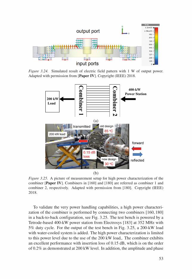
Figure 3.24. Simulated result of electric field pattern with 1 W of output power.Adapted with permission from [Paper IV]. Copyright (IEEE) 2018.
(a)
(b)Figure 3.25. A picture of measurement setup for high power characterization of thecombiner [Paper IV]. Combiners in [160] and [180] are referred as combiner 1 andcombiner 2, respectively. Adapted with permission from [180]. Copyright (IEEE)2018.
To validate the very power handling capabilities, a high power characteri-zation of the combiner is performed by connecting two combiners [160, 180]in a back-to-back configuration, see Fig. 3.25. The test bench is powered by aTetrode-based 400-kW power station from Electrosys [183] at 352 MHz with5% duty cycle. For the output of the test bench in Fig. 3.25, a 200-kW loadwith water-cooled system is added. The high power characterization is limitedto this power level due to the use of the 200 kW load,. The combiner exhibitsan excellent performance with insertion loss of 0.15 dB, which is on the orderof 0.2% as demonstrated at 200 kW level. In addition, the amplitude and phase
53

Figure 3.26. A block diagram of the sub-block 10-kW amplifiers with time-domainmeasurement setup. Adapted with permission from [Paper V].
imbalances among the ports are 0.1% and 0.036o, respectively. It is concludedthat the proposed combiner is well-suited to be used as a second combinationstage (i.e. in Fig. 3.18 the combiner carries 12 sub-blocks of 10 kW to real-ize power combination of 120 kW.) that is required for power capability up to400 kWs.
3.4 Integration of solid-state high power generation forparticle accelerators
Integration process consists of two parts: system design and system-levelcharacterization. In the system-level characterization procedure, the system[Paper V] is fully characterized under ESS specifications [8] using the time-domain setup described in [Paper II].
3.4.1 Integration of sub-block 10 kW amplifiersThe conceptual 400 kW system (i.e. in Fig. 3.18) is based on a number ofsub-blocks of 10 kW amplifier system [Paper V]. Fig. 3.26 shows the blockdiagram of the 10-kW sub-block. Each of the modules delivers more than1 kW output power at the frequency of interest, allowing for minimizing thenumber of ports to achieve 10 kW, thus, reducing the complexity of the com-bining topology. The 10-kW system is modular and it consists of 8 individualamplifier modules [Paper I]. The construction is integrated in a standardized
54

Figure 3.27. A picture of 10 kw system housed in 19-inch 3U rack with 4 modules onthe top and 4 modules at the bottom. Reprinted with permission from [Paper V]
.
19-inch 3U rack around a water-cooled heatsink in which 4 of modules areon the top and 4 of modules are at the bottom. The cooling system used forthe 10-kW system includes a cold aluminum plate and a water cooling pipeinserted in the middle of the plate, for thermal dissipation. The water inlettemperature is kept around 30o C with minimum water flow of 15 l/min. Apower supply (EA-PS 9063-90 from Elektro-Automatik) with high efficiencyprovides the DC power to the amplifiers using a capacitor bank as mentionedin section 3.2. The capacitor bank is composed of eight of 68-mF capacitors tostore energy within the pulse, one capacitor for each of the associated modules[Paper I] [8]. In addition, current breakers are used to implement measure-ments of the graceful degradation [162] by switching off DC power supplyapplied to a certain number of associated modules. DC power consumptionof the amplifier modules are monitored, as described in [Paper II]. All of thecollected data is then analyzed for system efficiency calculations. Calibrationprocess of voltage and current sensors is required for an improved accuracy.The test bench shown in Fig. 3.26, has a driver amplifier, a two-stage am-plifier including a linear amplifier (ZHL100W-52+) from Mini-circuits. Theoutput from the driver stage is splitted by a quarter-wavelength divider, whichis required to operate at about 200 W. The 1:8 divider distributes the RF sig-nal to each of the amplifier modules. To produce 10 kW of output power, an8:1 combiner is used to combine the output signals from the amplifier mod-ules. The combiner [99] is based on Gysel configuration [154]. Challenges
55

Figure 3.28. Drain efficiency of amplifier module [Paper I] at several drain voltages.
related to the microstrip technology integration with stack arrangement aresolved with a stack arrangement, as reported in [99]. The stack arrangementresults in a high degree of compactness despite the 352 MHz frequency witha quite long wavelength. In the layered approach, issues related to the ven-tilation capabilities are settled by using cut-out slots carried on layer-to-layerboards. Board-to-board coupling can cause a degradation of the combiner’sperformance, even worst in the stacked approach. To reduce the mutual cou-pling among boards, stubs are added in the common layer of the combinerand are located λ
8 from the floating common point. The full design of thedivider/combiner is further described in [Paper V].
Integration is a sequential step-by-step process. Firstly, every single com-ponent of the system is validated to make sure that it meets key performanceobjectives, depending upon the stage where it is located, i.e. footprint, har-monic levels, required output power levels, noise, insertion loss, stability, etc.In this section, the integration process is realized in three stages: driver stage,dividing/combining stage, and amplifier stage.
An amplifier stage:The first step is to realize the mechanical mounting of transistors to heat-sink.Steps should be taken to avoid any burn-out during high power operation, asfollows:• All holes are clear screw fastener with 3 mm in diameter. A lock washer
should also be used.
56

• It is recommended to keep mounting surface flat for the matching boardsat the input and output.
• At the bottom of the active device, a thin layer of thermal compound isused with no more than a thickness of 0.03 mm.
The second step is to realize the electrical connections following the stepsbelow:• Applying 50 V from power supply EA-PS9063-90 to the capacitor bank.
Supply cables are twisted using ferrite beads to diminish mutual inter-ferences. All of amplifier modules can be operated between 48 V to upto 52 V, see Fig. 3.28, however, the modules are optimized for 50 V at1250 W.
• All units are set to 40 mA quiescent current per transistor (2 transistors ineach package) at drain voltage of 50 V. The monitoring boards [Paper II]including the bias circuitry provides the gate bias voltage to the modules.Note that the bias point of 80 mA offers the best compromise betweenefficiency and gain.
• By-pass capacitors should be chosen properly at DC voltages to avoidspurs and instability during the operation of the modules.
The 3rd step is to characterize the imbalance in power and phase shift amongthe modules followed by a tuning procedure, allowing to keep variations withinreasonable limits, i.e. 0.5 dB in amplitude and 5o in phase, to reduce combin-ing loss [58, 151]. The tuning procedure is realized at both input and outputmatching networks. Due to manufacturing tolerance of active devices, pas-sive components, tuning procedure implemented at each of amplifier modules[Paper I] is varied, though the steps are similar. Depending upon the numberof input ports, the tuning procedure can be relaxed to some degree as demon-strated in [58] i.e. ± 5o in phase and ± 0.5 dB in amplitude among the 16amplifier modules [184]. The use of 8 amplifier modules in the 10 kW sub-block requires a more stringent tuning process with limits of amplitude andphase variations on the order of ± 0.25 dB and ± 2.5o, respectively. As men-tioned at step 2, the tuning procedure is optimized for 50 V at 1250 W outputpower. Details of the tuning procedure at each of the amplifier modules canbe found in Table 3.1. The current consumption is varied when moving thematching capacitor closer or further from the transistor. Initially, the distancebetween output matching capacitors and active device of all amplifier modulesis in the order of 1.6 cm. During the tuning process, trade-offs are made amongthe return loss, output power, and efficiency. Depending on the trade-offs, thedistance is adjusted, see Table 3.1. The tuning process includes:• Step 1: Adjusting gate voltage bias and measuring the quiescent current.• Step 2: Evaluating the performance of amplifier module regarding out-
put power, current consumption, gain, efficiency using the time domainmeasurement setup [Paper II].
• Step 3: Realizing tuning procedure.• Step 4: Return to step 2.
57

Module Tuning procedure
1 Vg = 1.58 V
Idq = 86 mA
Use of 10 pF + 8.2 pF + 6.8 pF for inputmatching at C5.Use of 27 pF and displace 1.8 cm far fromtransistor for output matching
2 Vg = 1.69 V
Idq = 88 mA
Use of 33 pF + 15 pF for input matching atC5.Use of 27 pF and displace 1.68 cm far fromtransistor for output matching
3 Vg = 1.57 V
Idq = 88 mA
Use of 33 pF + 10 pF + 3.7 pF for inputmatching at C5.Use of 27 pF and displace 1.6 cm far fromtransistor for output matching
4 Vg = 1.57 V
Idq = 88 mA
Use of 33 pF + 15 pF + 1 pF for inputmatching at C5.Use of 27 pF and displace 1.4 cm far fromtransistor for output matching
5 Vg = 1.58 V
Idq = 85 mA
Use of 33 pF + 8.2 pF + 6.8 pF for inputmatching at C5.Use of 27 pF and displace 1.75 cm far fromtransistor for output matching
6 Vg = 1.58 V
Idq = 84 mA
Use of 33 pF + 10 pF for input matching atC5.Use of 27 pF and displace 1.95 cm far fromtransistor for output matching
7 Vg = 1.59 V
Idq = 85 mA
Use of 33 pF + 10 pF for input matching atC5.Use of 27 pF and displace 1.75 cm far fromtransistor for output matching
8 Vg = 1.63 V
Idq = 86 mA
Use of 33 pF + 12 pF for input matching atC5.Use of 27 pF and displace 1.55 cm far fromtransistor for output matching
Table 3.1. Tuning procedure for each of the eight amplifier modules. The tuning pro-cedure is included and consists in adjusting: gate voltage and input/output matchingtuning.
58

(a) (b)Figure 3.29. Measurement results of one amplifier module during the tuning proce-dure. Output envelope of the RF pulse (left) and current waveform (right).
(a) (b)Figure 3.30. Optimal output waveform and drain efficiency waveform in time domainwith different amplifier modules at 1250 W. Reprinted with permission from [Paper
V].
• Step 5: Assessing the tuned performance with the requirements of inputreturn loss, output return loss, output power and efficiency.
The tuning procedure for one module with several power levels is shown inFig. 3.29. Insights of time domain measurement results with all of 8 amplifiermodules can be seen in [Paper V]. All of amplifiers are optimally tuned todeliver 1.25 kW average output power along with more than 70% in efficiencywithin the pulse. The droop, caused by the capacitor bank, is in the order of0.25 dB for all of modules [Paper V], see Fig. 3.30.
The combining stage:The goal is to realize the power summation of the individual modules in
order to achieve the targeted output power with minimum degradation in thecombining efficiency. Output loss is a figure-of-merit allowing the charac-terization of the combining efficiency. Such loss is influenced by combiner
59

topology, amplifier characteristics, device failures, and S-parameters of com-biner structure [58]. For the combining stage of the presented 10 kW system,some considerations must be taken, as follows:• The combiner structure should offer low insertion loss, matching at input
and output ports along with a good power handling capability.• The failure of a module causes a reduction in the output power propor-
tional to (1− kN )
2 in which kN is the fraction of failed devices [58]. A
good combining structure means a good isolation among the ports toavoid any degradation once a failure happens.
• When choosing combiner structure, reliability is an important factor toconsider. The reliability at the combining stage should be far beyond ascompared to the reliability at the amplifier stage and at the driver stage.
• Connectors at combiner terminations should be capable of carrying highpower even in case of mismatch. Interconnection losses between con-nectors and transmission lines should be minimized i.e. in [Paper II]and [99].
• Design of the combiner should be of small footprint, cost effectiveness.For the dividing stage of the 10 kW sub-block, the divider is required to
distribute about 20 W to each amplifier modules. A quarter-wavelength coax-ial configuration is chosen. The divider offers low insertion loss i.e. 0.05 dB,return loss of 25 dB, and isolation of 8.33 dB among the ports. Details can befound in [Paper V]. For the combining stage, the choice goes to a Gysel-basedapproach realized on planar technology with stack arrangement allowing fora reduced footprint. Reduced footprint results in an increase of the mutualcoupling among transmission lines. This is also used to reason to degrade thebalances among the ports in amplitude and phase. A tuning solution is in-vestigated using coupling stubs in order to reduce the mutual coupling, thus,enhancing the isolation up to 20 dB and phase imbalance within 4o. The tuningprocedure in the dividing/combining stage consists of the following steps:• Choosing the topology of divider/combiner based on the targeted output
power, power handling capability i.e, in the 10 kW, the number of PAs isfixed with 8 modules.
• Measuring divider/combiner’s characteristics including: amplitude andphase imbalances, isolation, return loss.
• Depending on the phase variations among ports at the divid-ing/combining stage and the amplifier stages, each of the amplifiers ischosen to be connected to a suitable port at the combining stage to reduceany imbalances, see Table 3.2. Other solutions can be realized including:using variable-length cables or using gain/phase variable modules [185]at each of amplifier module. However, these solutions are complicatedand costly and will not be covered in the scope of the thesis.
For the driving stage:For the driving stage, it is very flexible to design the architecture of the
stage. There is no restriction of how many stages it supposed to have, but it is
60

Divider Stage Amplifier Stage Combiner StagePort 2 Amplifier 1 Port 3Port 3 Amplifier 2 Port 5Port 4 Amplifier 3 Port 8Port 5 Amplifier 4 Port 7Port 8 Amplifier 5 Port 4Port 7 Amplifier 6 Port 2Port 6 Amplifier 7 Port 1Port 1 Amplifier 8 Port 6
Table 3.2. Inter-stage connections among components in 10 kW system for compen-sating imbalances.
Figure 3.31. Characteristics of driver stage in the presented 10 kW system.
influenced by the input from the LLRF controller and output power needed forthe dividing stage. Care should be taken for linearity at this stage. Linearityis an important factor for realizing the control loop, which will be presentedin the following. The driving stage should also provide a margin of 10-15% inoverhead power to compensate the losses of RF cables and circulator, as canbe seen in Fig. 3.26.
3.4.2 System-level characterizationSystem-level characterization is realized in time domain once all of stages inthe system are connected and tuned following the tuning process, previouslydescribed. Combining loss is a valuable figure-of-merit at the system-levelcharacterization. The combining loss reflects how good the integration pro-cess could be. As can be seen in Fig. 3.32, there is a significant loss at theoutput of low power levels, which tends to diminish at the nominal outputpower delivering output power below 6 kW whereas the loss is minimized as
61

Figure 3.32. Combining loss of the 10 kW sub-block system. Reprinted with permis-sion from [Paper V].
each of amplifier modules reach 1 kW.Since the imbalances in amplitude andphase among the modules are not optimized at such power levels. The overallcombining loss at high power level is only on the order of 0.15 dB, equivalentto approximately a 3% loss in power. Due to the use of the storage capacitorbank, there is a drop at the output power envelope of the 10 kW sub-block,see Fig. 3.33. The drop is measured on the order of 1 kW within the pulse,which is equivalent to 0.36 dB. The drop within the pulse is due to the use ofcapacitor bank required in pulsed operation. The power drop causes instabili-ties in the linac which could lead to the acceleration of charged particles withinconsistent energies. We need to address this issue when developing solid-state amplifiers for particle accelerators operated in pulsed mode. A feedbackcontrol loop is realized allowing for stabilizing the amplitude and phase dis-turbances of the RF 10 kW system and compensating the drop caused by thecapacitor bank. The control loop is implemented by an LLRF system devel-oped at FREIA. Fig. 3.34 shows a block diagram of the proposed system. Thecontrol loop is based on Proportional-Integral (PI) controller implemented onthe platform FlexRIO NI-5782 from National Instruments. More insights ofthe architecture can be found in [Paper V]. A reference signal is coupled tothe output of 10 kW subblock system and is used as the reference signal ofthe control loop. The reference signal is then fed to the control loop. Theimplementation of the control loop includes the following procedure:• Use LLRF to generate the RF pulsed signal at 352 MHz instead of using
a vector signal generator. Calibration process is realized at this step.• Open-loop testing with LLRF controller (no feedback) to evaluate the
linearity of the system versus output power levels.
62

Figure 3.33. Output power and DC power waveforms at 10 kW power level. Reprintedwith permission from [Paper V].
Figure 3.34. A block diagram of 10 kW system along with the feedback control loop.Reprinted with permission from [Paper V].
• Running the feedback loop in amplitude and phase at low power levels.Increasing power levels from low to 1 kW as to avoid any instabilitywhich could damage the amplifiers.
• Once the system works properly, the system-level is operated in severalhours i.e. at least 4 hours and the RF 10 kW sub-block is characterizedin operation.
3.4.3 Summary.This thesis work developed in details the design, manufacturing and charac-terisation of a 10 kW solid-state amplifier starting from modules to the systemintegration. This work allows for a scale-up in power (i.e. targeting 400 kW)
63

Figure 3.35. Measurement results of 10 kW system with compensated drop at theflat-top. Reprinted with permission from [Paper V].
to be used for next generation particle accelerators i.e. ESS superconductingcavities. Combining loss, pulse drop and stability are needed to characterizehigh power pulsed amplifiers using solid state technology. All of these needto be fully characterized using time-domain measurement setup in [Paper II].A feedback loop [Paper V] addresses the pulse drop issue by using a PI-basedcontrol strategy in order to pre-distort the input signal for compensating theinherent droop caused by capacitor bank. In addition to pulse drop, the am-plitude and phase stability also can be improved with the feedback loop. Itis demonstrated that there is arcing, sudden heating, or degradation in perfor-mance of the 10 kW system during long hours of operation when delivering10 kW output power. The system can be operated with 10-20% margin ofoutput power in case of failure modules.
64

4. An experimental investigation of theoptimal filling scheme for possibleconceptual architectures of the 400 kWsystem.
This chapter discusses the scaling up in power of the conceptual design of400 kW starting from the sub-block of a 10 kW power amplifier, as presentedin Chapter 3. Fig.4.1 shows a system design of sub-blocks layer-over-layerassembly consisting of controller system, dividing/combining stage, capacitorbank, AC/DC power supply, and cooling system. Depending on the targetedoutput power, the choice of combiner topology and available power deliveredby the modules are of paramount importance. The output from each of the sub-blocks is fed to a passive combining stage for realizing the power combinationtill 400 kW. In this chapter, several combining strategies will be discussedbased on 10 kW amplifier sub-blocks. The strategies are described in [Paper
III] and [Paper IV]. For all of these combining strategies, there is a demand ofa distribution network which is based on a WR-2300 half-height wave-guide.
Figure 4.1. A block diagram of full sub-block design. A number of sub-blocks areused for combining 400 kW of output power.
65

Figure 4.2. A schematic outline of the combining network I. Adapted with permissionfrom [160].
The wave-guide-based system allows distributing high power to the cavitieswith low loss.
In the second part of this chapter, we discuss the realization of an optimalcharging scheme [13] using solid-state amplifiers. This scheme is demon-strated using an envelope tracking technique applied to a kW-level module.The proof-of-concept of this design is realized in [Paper VI]. In this paper,we demonstrate the feasibility of implementing the optimal charging schemeon solid-state amplifiers for the next generation particle accelerators using SCcavities in pulsed mode with minimized reflection, energy-saving operationup to 24% in total [Paper VI]. The experiment-based results shown in [Paper
VI] unlock a new way to efficiently operate high power RF systems for nextgeneration particle accelerators. In addition to merits of this scheme, a sig-nificant reduction of reflection power during filling time i.e. 400 kW in caseof ESS superconducting cavities, is obtained. This allows for reducing therequirements of the sub-components i.e circulators for protection, the rugged-ness of the PA modules, thus leads to cost-effectiveness, and reliable systems.
4.1 The possibilities of 400 kW conceptual designsusing 10 kW sub-blocks and high-power combiningsolutions.
The core technology is the single-ended architecture and different combiningstrategies are demonstrated in Chapter 3. The demonstration of the powercombination at 10 kW level allows foreseeing the possibility for scaling up inpower of 400 kW. To realize this implementation, it is important to discuss theconceptual possibilities of the combining architectures and investigate advan-tages and disadvantages, thus discussing the best choice for a 400 kW solid-state based power station for the ESS accelerator facility.
66

Figure 4.3. A schematic outline of the combining network II.
Combination strategy 1:
As can be seen in Fig. 4.2, 48 sub-blocks of 10 kW represent 384 kilowatt-level amplifier modules. There are four groups of amplifiers, each including12 modules. The outputs are then fed to 12-way combiners in [Paper IV]. Thefollowing combining stage is based on half-wave-guide (WR2300) combiner.The high power combiner realizes power summation of 100 kW inputs allow-ing for delivering 400 kW output power. Coaxial 3-1/8” connectors are usedfor interconnecting combining stage 1 and stage 2. Details of design can befound in [Paper VI].
Advantages:• Ultra high power carrying capability.• A section of power transmission line for final power combining, i.e.
WR2300 half-height wave-guide, could avoid the use of extra connec-tors and adapters.
Disadvantages:• Large-size design.
Combination strategy II:
The second combining strategy makes use of two stages of combining, in-cluding: binary combiners and 12-way combiners in [Paper IV] for highpower levels. The binary combiners adopt the strip-line technique described in[Paper III] for combining a group of 4 sub-blocks. The output of the binarystage is in the order of 40 kW. At the last stage, it is based on a wave-guidecombiner, similar to the one introduced in the strategy 1. This configurationallows for the combination of 12 outputs from the binary stages, see Fig. 4.3.Coaxial 3-1/8” connectors are used for high power connecting stage 1 andstage 2. Advantages:• Use of striplines makes the design more compact.• Good isolation design.• Advantages of Gysel-based configuration once mismatch happens.• Tuning process is more accessible.
67

Figure 4.4. A schematic outline of the combining network 3 with resonant structures.
Disadvantages:• External loads at the binary stages are needed. An associated cooling
system for the loads should be included.• High power transition between striplines and output connectors could
cause losses and might be difficult to design.
Combination strategy III:
Cavity and radial combiners are becoming more and more available at acceler-ator facilities, i.e. at ESRF [111], CERN [186]. In the multi-port combiner de-signs, the number of the inputs can be extended up to dozens i.e. 144 inputs atCERN’s cavity combiner design. In the combination strategy III, we considerthe conceptual design of 400 kW using a 400:1 cavity combiner stage, 400kW-level modules, and their associated driver amplifiers. This strategy allowsto eliminate the use of the dividing stage, see in Fig. 4.4. Each of the 400 driveramplifiers is fed by a single direct digital synthesis (DDS) based module, al-lowing the generation of a digital signal. Each of 400 DDS-based modules iscapable of adjusting amplitude, phase, and frequency. A synchronized clockinterface is needed for the synchronization among i.e. the DDS-based signalgenerators or phase-locked loop for the synchronization of voltage-controlledoscillators. The cavity combiner in this configuration allows the capability of
68

Figure 4.5. Pulse profile in time domain in case of conventional filling scheme andoptimal filling scheme. Reprinted with permission from [Paper VI].
tuning at the input coupling ports by implementing movable coupling struc-tures, as described in [111].
Advantages:• The combination strategy allows implementing the optimized feeding
power profile for operation with SC RF cavities.• This configuration is highly tunable and adaptive, thus it results in a
highly efficient, reliable system that could self-adapt to unpredictablesituations.
Disadvantages:• The processor board used to control 400 DDS-based modules might be
complicated.• The realization of the control strategies is challenging i.e. when control-
ling 400 modules as required at ESS facility.
4.2 Proof-of-concept kilowatt-level design system foroptimal charging scheme.
The optimal charging scheme [13] allows significantly reducing power reflec-tion when charging superconducting cavities as compared to the conventionalstep-filling scheme. For ESS spoke cavities [8], the wasted energy caused byfull power reflection in the step filling process is estimated to be in the orderof 30 MWh during long operation, i.e. 8000 hours. Estimates of the wastedenergy are even worse for medium-β and high-β cavities at 150 MWhrs and
69

Figure 4.6. The pulse profile in time domain for one module as a function of time.Reprinted with permission from [Paper VI].
550 MWh, respectively [187]. Thus, the energy savings of 730 MWh in totalwith 684 e/MWh brings a reduction of the annual cost of 500 Ke. Therefore,it is necessary to implement the optimal control scheme during the filling timeof cavities allowing for accelerator designs towards sustainability and energyefficiency, as presented in Chapter 1.
The combination strategy I in section 4.1 is considered for the optimalcharging scheme. The pulse profile in time domain is shown in Fig. 4.5. Dur-ing a period of about 300 μ s, the RF power increases exponentially till thenominal power level. The power generation system based on SSPAs suffersof a sub-optimum efficiency i.e. at low and medium-range power level theefficiency of the amplifiers is rather low. To realize an optimal charging, theefficiency of the solid-state based generation system, using envelope trackingtechniques, is highly increased. The implementation is realized on a kilowatt-level module as a proof-of-concept. This proof-of-concept design could bethen scaled up in power till the nominal 400 kW using passive components, ascan be seen in 4.1.
4.2.1 A proof-of-concept design for optimal charging scheme.Envelope tracking (ET) is a well-established technique in communication sys-tems [188–190]. In this thesis, we have adapted this technique to the single-ended kW module described in [Paper I] in pulse operation referring to thepulse profile in Fig. 4.6. The realization on the kilowatt-level module in[Paper I] consists of two parts: one is to generate an input RF signal fol-
70

lowing the shaping function in Fig. 4.6, the other part is to apply the generatedshaping signal for the envelope tracking amplifier module.
Generating the input shaping function:The shaping function generator makes use of a field-programmable gate ar-ray (FPGA) platform KC705 from XIlinx [191] and a quad-channel 16-bitDAC34SH84EVM from Texas Instrument [192]. The shaping function is rep-resented by a mathematical expression as follows:
f (t/ f ) =
⎧⎪⎪⎨⎪⎪⎩
K1∗1010log10
e(Xrise(t/ f )∗K2)2
K3∗(sinh(2))2−10
20 if 0≤ t ≤ 300μs1 if 300μs < t ≤ 3.5ms0 elsewhere
(4.1)
where K1, K2 and K3 are fitting parameters and f is the sampling frequency.These parameters are adjusted to fit the shaping function as provided inFig. 4.6. A script written in Verilog Hardware Description Language (VHDL)is then used to implement the shaping function with a clock of 125 MHz.The KC705 platform transmits the data to a DAC34SH84EVM via 32-bit low-voltage differential signaling (LVDS) interface. The LVDS data goes througha multi-stage interpolation filter before feeding the digital mixing stage. Agraphic user interface (GUI) provided from Texas Instruments is used to setdifferent parameters via a serial interface i.e. frequency of built-in frequency(NCO), number of interpolation filters, gain of digital-to-converter (DAC),programmable delays, etc. A wide-band transformer [193] in combinationwith a matching network allows to convert the 32-bit LVDS output to a 50 Ωunbalanced output for the proof-of-concept amplifier in [Paper VI]. Detailscan be found in [Paper VI].
Implementation of the envelope tracking solution:The proof-of-concept envelope tracking system consists of several compo-nents, including: a fast-switching power supply modulator (SM52-30 fromDelta Elektronika), FPGA-based signal generator, driver stage, kilowatt-levelsingle-ended amplifier module in [Paper I], and a measurement setup as de-scribed in [Paper II] in time domain. The signal generator produces an en-velope control shaping function allowing to control dynamically the supplymodulator . The envelope control function is tailored from Eq. 4.1 in the formof a time domain modified function Mopt , as follows:
71

Figure 4.7. Control voltage and drain voltage of the proof-of-concept design as afunction of time. Reprinted with permission from [Paper VI].
Mopt(t/ f ) =
⎧⎪⎪⎪⎪⎪⎪⎨⎪⎪⎪⎪⎪⎪⎩
0.3815 if−200μs < t ≤ 0
7.75∗1010log10
e(Xrise(t/ f ))2
4∗(sinh(2))2−10
20 if 0≤ t ≤ 300μs1 if 300μs < t ≤ 3.5ms0 elsewhere
(4.2)
The modification of Mopt depends mostly on the supply modulator’s char-acteristics, and modes of operation of the envelope tracking amplifier [194] asdescribed in [Paper VI], see Fig. 4.7. Care should be taken for the time align-ment between the envelope control path and the RF pulsed signal path. Thetime alignment is programmable in a FPGA platform and is adapted to achievethe best performance in terms of efficiency. The capacitance at the drain ofthe proof-of-concept design is removed as to allow the fast supply modulation,following the recommendation in [195,196]. This might lead to instability dueto the low capacitance at the drain terminal. A measurement setup in time do-main is used to characterize the performances of the proof-of-concept designregarding output power waveform, efficiency waveform, especially during thefirst 300μs that are particularly of interest.
As can be seen in Fig. 4.7, the supply modulator exhibits saturation whensupplying the amplifier in the high power range. This inhibits the linearityof the amplifier, as described in [Paper VI] when full power is reached (i.e.the transition region prior to the flat-top of the pulsed RF). In this thesis, a
72

(a) (b)Figure 4.8. (a) Output power and DC power waveform as a function of time withand without the linearized approach. (b) Efficiency as a function of time in case ofconstant drain voltage and dynamic drain voltage. Reprinted with permission from[Paper VI].
linearized function is implemented in order to enhance the linearity for theproof-of-concept design. More insights can be found in [Paper VI].
4.2.2 Results and discussionsCharacterization results:
Efficiency waveform is clearly an important figure-of-merit for the charac-terization of the envelope tracking (ET) system as described in [Paper VI].The efficiency of the ET system is characterized in terms of the efficiency ofthe amplifier module [Paper I] associated with the efficiency of the supplymodulator (SM52-30), as follows:
ηET_system = ηSM×ηSSPA (4.3)
The characterization of the supply modulator (SM52-30) is performed us-ing a power analyzer (PCE-830) allowing for measuring the input power witha constant nominal 230 VAC. At the output load of the supply modulator, thevoltage and current sensors record the measure of the output power with highaccuracy. For the efficiency of the amplifier module described in [Paper I], adedicated measurement setup is realized in time domain which allows to char-acterize the amplifier’s efficiency waveform, output power waveform, currentwaveform, and voltage waveform. Some preliminary results shown in Fig 4.8,are compared to the obtained results with a fixed drain voltage of 50 V. A sig-nificant improvement in efficiency at low and medium-range power levels isobtained when applying the optimal shaping profile with the envelope trackingtechnique. The results allow to validate the energy efficiency improvement andnew power amplifier design approach to practically implement optimal charg-
73

ing scheme for very high power system using the solid state technology [13].The over-arching realization would allow reaching key objectives i.e. the de-velopment of greener and more sustainable Big Science infrastructures.
Discussions:
Implementing the envelope tracking modulation at 400 kW would allow a sig-nificant reduction of the energy consumption up to 24% in addition to a min-imized reduction of reflection power during the charging time. For a largesystem, a valuable figure-of-merit Rwall , as defined in [13], is used allowingfor analyzing the benefit of the optimal charging scheme as compared to thestep filling scheme. From the theoretical analysis realized in [13], it is con-cluded that the particles should be injected at an optimal cavity charging timeof 1.5 times the cavity step filling time for best performance of the energyconsumption. The optimal charging time is then computed on the order of312 μs. As a result, the value of the energy savings from wall plug Rwall canbe represented as a function of charging time with respect to other establishedtechnologies in accelerator community, see Fig. 4.9.
The analysis of Rwall demonstrates the optimal filling scheme is most suit-able to the solid-state based amplifiers in comparison with other types of am-plifiers i.e. Tetrodes, and Klystrodes. The feasibility study of the optimal fill-ing scheme is realized in this chapter and the results have the potentials to in-spire the next-generation particle accelerators to adopt the solid state technol-ogy, as the technological choice for envelope-tracking energy-efficient poweramplifiers.
74

Figure 4.9. Energy efficiency Rwall as a function of charging time with several tech-nologies i.e. Tetrodes, Inductive Tube Outputs (IOTs), and ET amplifiers in [Paper
VI]. Reprinted with permission from [Paper VI].
75

5. Conclusions and future works
5.1 ConclusionsThis thesis contributes to the development of the next generation RF powersystems for particle accelerators in Big Science projects, implementing the lat-est solid-state technology (i.e. LDMOS) and high power low loss combiningstrategies. One new design is introduced, the single-ended architecture at kilo-watt level based on a two-stepped impedance matching network. The work isrealized for the European Spallation Source (ESS) specifications i.e. 352 MHzpulsed mode operation with 5% duty cycle. The design approach in [Paper
I] combined with advances in LDMOS technology results in a superior per-formance design for pulsed operation. Time-domain characterization methodsare improved in [Paper II] and are applicable to extend for the measurementsat higher frequency and higher power levels.
In this thesis, new engineering solutions for the power combination are pro-posed and realized [Paper III and Paper IV]. These solutions focus on power-handling capability, compactness, low loss and cost reduction. Suspended-stripline technology with air dielectric results in extremely low loss powercombiner. The re-entrant cavity in combiner with doornob-based geometry[Paper IV] allows for an excellent performance of 0.2% insertion loss, 0.1%amplitude imbalance, 0.036o in phase spread among ports and good thermalproperties for high power combination. Other high power tests demonstrate thepower handling capability of these solutions at 20 kW peak power level for 2-way combiner in [Paper III] and 100-kW peak power level for 12-way cavitycombiner in [Paper IV]. These engineering solutions presented in this thesisare suitable for mid-range and high-range power level up to a few hundreds ofkilo-watts. The demonstration of a 10 kW SSPAs [Paper V], which is thenconsidered as an elementary block supporting the engineering discussion forscaling up in power till 400 kW, the nominal power per SC RF cavity at ESSlinac. To the best of our knowledge, the presented system is by far improv-ing the state-of-the-art in terms of efficiency and compactness for a system at10 kW power level and at 352 MHz. Insights of system design presented inthis thesis can be used as baseline for the integration of the next generationparticle accelerators. With the LLRF controller demonstration of the compen-sation and stabilization of the power delivered are essential for the scale-up inpower required for the accelerating structures [Paper V]. The demonstrationof the droop compensation is realized, using a digital feedback loop and theresults show 0.4 dB droop within the pulse is compensated when operating at10 kW output power level.
76

This thesis investigates and gives solutions for more and more actual chal-lenge which is of energy efficiency and reduction of the wasted energy due tomismatch during the filling period of accelerating cavities. For the first time,an optimal charging scheme is applied using a solid-state based amplifier with-out degrading the efficiency during operation i.e. the system is ramped-up inpower to charge cavities, low reflection levels from the SC RF cavity. Thisis facilitated by realizing a very fast envelope tracking power supply (ETPS)operated over a charging time of 300 μs, as would be required by ESS [8]. TheETPS system is implemented on a single module and it is possible to realizethe up-scaling in power till the nominal power level of 400 kW. This thesis dis-cusses some of the possible architectures based on the demonstrated the ETPSmodule and gives a calculated improvement of just 24% of energy savings incomparison to the step filling scheme. The results of this thesis will facilitatethe development of sustainable next generation particle accelerators in NewBig Science projects and other future high power applications, all using solidstate power amplifiers.
5.2 Future WorksSome of the future works that the author believes are highly relevant and in-teresting to be considered.• In accelerator community, reliability is of paramount importance since
the accelerator facilities require stringent demand of availability. There-fore, the reliability analysis of solid-state based power generation sys-tems is paramount. A feasible extensive of the measurement setup in[Paper I] can be performed as a smart testing system with capabilityof harvesting sensors data and extracting the RF behavior towards theprediction and avoidance of failure i.e. stress tests, and optimizing RFamplifier’s properties, and increasing its reliability.
• After successful demonstration of the proof-of-concept design presentedin [Paper IV], a higher integration could be developed considering in-dividual DC modulators instead of using commercial ones as in [Paper
VI]. This will facilitate the integration that is required high power i.e.400 kW for ESS spoke cavities. In addition to this, using individual sup-ply modulators helps implementing corporate-combining architecture incase of using multi-inputs separately without the use of divider stage.
• The ultimate goal of this thesis is to provide a methodology allowingfor implementing high power high efficiency power systems requirednot only in accelerator applications but also in other higher-frequencyapplications. For these purposes, it would be interesting to address allof this work on GaN technology at high power levels i.e. hundreds ofkilowatts, or even MW, aiming to fully replace tube amplifiers in futuresustainable systems.
77

6. Summary of the papers
Paper [I]: Kilowatt-level power amplifier in a single-ended architecture at 352
MHz
In this paper, a design approach of single-ended kW-level SSPA isadopted. The feasibility of single-ended architecture is demonstratedallowing for delivering more than 1.25 kW peak power in deep class ABunder ESS specifications (352 MHz RF pulsed with 5% duty cycle). Thedesign in [Paper I] is also tested in CW operation, however, efficiencydrops to 60% due to thermal issue. To the best knowledge of authors,the design achieves a high efficiency of 71%. The adopted architectureopens up a new perspective towards kilowatt-level power amplifiers witha similar efficiency and output power, without requiring more complexcircuits structures,such as baluns. This, therefore, contributes to improv-ing the competitiveness of solid-state based power generation systemsi.e. low manufacturing cost, ease for tuning and scaling in power, etc.
Paper [II]: Time domain characterization of high power solid state amplifiers
for the next generation linear accelerators
For next-generation linacs i.e. ESS linac, the requirements of RF powersources are stringent regarding output power, efficiency, amplitude andphase stability. Characterizing SSPA modules of such power sourcesplay an important role to validate PA design, thus reducing the designcycle. This paper presents the time domain characterization of highpower pulsed solid state amplifiers in [Paper I] to be used for linearaccelerator applications. All of PA properties are fully characterized inlarge-signal measurements when operating at kW level. In this paper, thetime-domain measurement setup allows measuring pulse-to-pulse (P2P)stability in both amplitude and phase, then gives insights to which factorsdegrade the P2P stability during high power operation. Since a degradedstability in RF power sources might cause instabilities in particle accel-erators when beam is injected i.e. no consistent energy is provided to theaccelerated particles.
Paper [III]: High-power low-loss air-dielectric stripline Gysel divider/combiner
for particle accelerator applications at 352 MHz
This paper focuses on an engineering solution to improve the powerhandling capability of a Gysel structure. The solution is based on anair-dielectric stripline which allows to handle very high radio-frequencypower levels with low-loss suitable for power combination in accelera-tor applications. A test of 2-way combiner using the proposed structure
78

is performed under 22 kW peak power level. The efficiency and powerhandling capability of the combiner are greatly improved by choosingappropriate thickness of striplines and using air as a dielectric. This en-gineering solution presented in this paper allows realizing combiners inthe mid-range power states of a few dozens kW level of power.
Paper [IV]: 12-Way 100 kW Reentrant Cavity-Based Power Combiner With
Doorknob Couplers
In this paper, we proposed an engineering solution of high power com-biner aiming for power-combining stage at hundreds of kW to be used in400 kW power generation system for ESS spoke cavities. The combineris based on a re-entrant cavity with 12 input doorknob couplers and oneoutput coupler that is integrated with the post of the cavity and formsdoorknob type geometry. The presented design allows for an excellentmechanical quality and RF performance i.e. 0.2% insertion loss and arelative rms amplitude imbalance between the ports of 0.1% and phaseimbalance of 0,036o rms, suitably for industrial mass production, simplescalability, and good thermal characterization for high power handling.A high-power test implemented at 200 kW (352 MHz pulsed RF, 5%duty cycle) in back-to-back configuration shows good RF loss to be com-parable to the low-power measurements and in the long run the combinertemperature stabilizes at 10o C above ambient.
Paper [V]: Feedback compensated 10 kW solid-state pulsed power amplifier at
352 MHz for particle accelerators
This paper presents insights of a modular and scalable 10 kW solid-statebased RF system, which consists of 8 single-ended amplifier modulesin [Paper I]. In the presented 10 kW system, the single-ended designapproach toward compactness, high stability, high efficiency, and easyrepeatability is validated at the kilowatt level, each of the power amplifiermodules delivering up to about 1.3 kW output power. The 10 kW systemuses a Gysel-based combiner realizing on the planar technology with alayer-by-layer approach. The layer-by-layer design approach makes theintegration of 10 kW realizable in the 4U rack unit. For the 10 kWsystem, a combination of 8 modules is demonstrated. For ESS specifi-cations, the SSPA-based 10 kW system exhibits 72% within the pulsein drain efficiency at 10 kW of output power. To best of our knowl-edge, the presented system is by far the best regarding compactness, ef-ficiency at 10 kW of output power at this frequency of interest. In thesecond part, we characterize the power droop due to capacitor banks inthe time domain. In open loop of compensation, it is about 1 kW withinthe pulse of peak value 10 kW and a duration of 3.5 ms. This maylead to the beam instability of the accelerator as particles are not pro-vided with the same energy during the pulse. The compensation usingan in-house LLRF is performed to facilitate the stringent requirementsof droop within the pulse. The feedback 10 kW system is a contender
79

for scaling up in 400 kW power required in ESS spoke cavities’ powergeneration systems.
Paper [VI]: A proof-of-concept design of a highly efficiency solid state RF power
source for Optimal Power Consumption during the charging of su-
perconducting cavities
This paper focuses on a very fast envelope tracking system (ETPS), real-izing theoretical developments related to an optimal charging in pulsedmodes of ESS SC cavities [13]. The ETPS is the first to demon-strate kilowatt power level envelope modulation with rising time asfast as 300 μs that would be required for ESS. This implementationis performed using an FPGA platform (KC705) along with ADC/DACboards, controlling both a fast DC power supply (SM52-30 from Delta-Elecktronika) and generating RF signals. For 400 kW system to powerESS spoke cavities, the use of optimal charging scheme in combinedwith the ETPS results in an improvement of 25% in overall energy sav-ings as compared to the conventional filling method (i.e. full power isprovided to cavities in the beginning). This demonstration opens a newparadigm in accelerator facilities when considering design of RF powergeneration systems for accelerating cavities towards minimized wastedreflection power during charging time, optimized efficiency while inhigh power operation, thus reducing overall energy consumption.
80

7. Sammanfattning pa Svenska
En losning som uppfyller krav pa effektivitet, komplexitet och kostnad ar ettmaste i RF-kraftsystem for acceleratordelen i nasta generations partikelaccel-eratorer. Denna avhandling handlar om design- och konstruktionslosningar foratt na en sadan losning. En slutsats fran avhandlingsarbetet ar att utvecklin-gen av nasta generations RF-kraftsystem kommer att implementeras med densenaste solid-state-teknologin (dvs. LDMOS eller GaN) och kombination-sstrategier for hog effekt. En single-ended arkitektur baserad pa en tvastegsimpedansmatchningsteknik anvands for att realisera en forstarkarkonstruktionfor effektnivaer over kilo-Watt. For att mota ESS-specifikationer vid pulseratlage pa 352 MHz ar LDMOS den teknologi som kan erbjuda hog effekttathet,hog effektivitet, och hog matningsspanning pa 50 V. Designmetoden i [PaperI] i kombination med sadana framsteg i RF LDMOS-teknologin resulterar ioverlagsen prestanda i pulserat lage for att erhalla hogre effektivitet, hog utef-fekt och samtidigt erbjuda enkel anpassning och massproduktion till lag kost-nad. Designmetoden i [Paper I] oppnar ocksa ett nytt paradigm for andra pul-sade hogeffektsystem som kraver kompakthet, effektivitet och effekt for andratillampningar, som t ex material-uppvarmning, kommunikation, radar, etc. Enstorsignals-matmetod for hogeffektmatning i tidsdoman [Paper II ] presenterasfor att fullstandigt karakterisera forstarkarkonstruktionerna [Paper I] vilketmojliggor kortare designcykler och anvandandet av hogre frekvenser. Kom-binerare (vilka anvands for att blanda flera effektsignaler) ar vanligtvis my-cket skrymmande strukturer i ett RF-kraftproduktionssystem. I denna avhan-dling foreslas tekniska losningar for nya strategier for kombinerare [PaperIV] och realiseras i [Paper III and Paper IV]. Dessa losningar fokuserar paformagan att hantera effekterna, kompakthet, laga forluster och kostnadsmin-skningar. I [Paper III] resulterar den upphangda stripline-tekniken med luftdielektrika i en extremt lag forluststruktur som implementeras pa en Gysel-baserad topologi, med 0.1 dB ingangsdampning vid 352 MHz. En annan kon-struktion av kombinerare i [Paper IV] mojliggor en utmarkt prestanda pa 0.2%i inforingsforlust, 0.1% i amplitudobalans, 0.036 grader i fasspridning mel-lan portarna och god termisk prestanda vid hoga effektnivaer. Hogeffekttestervisar effekthanteringsformagan hos dessa losningar vid 20 kW toppeffektnivafor 2-vags kombinerare i [Paper III] och 100 kW toppeffektniva for 12-vagskavitets-kombinerare i [Paper IV]. Dessa tekniska losningar som presenteras iavhandlingen ar lampliga for medium- till hogeffektniva. Design och integra-tionsmetoder som presenteras i avhandlingen kan anvandas for att forbattraprestanda for system som bestar av ett antal moduler inom kombinerande
81

arkitekturer. Designmetoden for [Paper I] bidrar till att framgangsrikt demon-strera en integration av 10 kW (Solid State Power Amplifier) SSPA: er [PaperV], som sedan anvands som byggblock, med stod for nya tekniska losningar,[Paper III och Paper IV] for att skala upp till 400 kW i effekt . Sa vittforfattaren vet ar det presenterade systemet overlagset bast nar det galler kom-pakthet, effektivitet vid 10 kW uteffekt. Insikter om systemdesign som presen-teras i denna avhandling kan ocksa anvandas som grund for att integrera ochrealisera hogeffektiva pulssystem som ska anvandas for nasta generations par-tikelacceleratorer. Det 10 kW SSPA-baserade systemet ar enkelt att integreramed LLRF-regulatorn for att kompensera och stabilisera systemegenskapernanar man utvecklar acceleratorerna. For forsta gangen utfors droppkompensa-tionen inom pulsen baserat pa PI-regulatorn [Paper V]. Vid implementeringenresulterar den digitala aterkopplingsslingan i att framgangsrikt kompensera for0.4 dB dropp i pulsen, vilket motsvarar 1 kW i effekt, vilket ar orsakat avanvandning av en kondensatorbank. Denna avhandling undersoker en intres-sant utmaning i alla acceleratoranlaggningar som har lag verkningsgrad un-der pafyllningsperioden, vilket orsakas av missanpassnings hos accelererandekaviteten nar man bygger upp det elektromagnetiska faltet inuti kaviteten.For forsta gangen tillampas ett optimalt laddningsschema pa en SSPA sommojliggor minimering av energireflexion utan att forsamra effektiviteten underdess drift, dvs systemet rampas upp for att ladda kaviteten. Detta underlattasgenom att realisera ett mycket snabbt envelope tracking power supply (ETPS),dvs ett styrbart spanningsaggregat, under en laddningstid pa 300 μs, som kravsav ESS [8]. ETPS-systemet implementeras pa en enda modul och kan realis-eras for att skala upp till 400 kW enligt proceduren som bescrivs i [Paper V].Avhandlingen diskuterar nagra mojliga arkitekturer baserade pa den demon-strerade ETPS och ger en beraknad forbattring med 25% i energibesparingarmed ett upprampat system, jamfort med stegfyllningssystemet. Resultaten idenna avhandling kan underlatta utvecklingen av nasta generations hallbarapartikelacceleratorer i nya stora vetenskapsprojekt och andra framtida applika-tioner med hog RF-effekt.
82

8. Acknowledgement
I took my very first steps in Uppsala during the dark, wet, and extremely colddays five years ago in November 2014. Today is also a rainy day that remindsme of the turning moment I never ever forget in my life. To me, it was hap-pening like yesterday. Every journey has an end and it is the time for my Phdjourney to come to an end with a happy ending. Even though the journey waslike a bumpy road with the chronic stress, long nights staying in the labora-tories, hours-long controversies to solve scientific problems along the way, itis very much enjoyable to find new things and to challenge myself. I herebywould like to take the opportunity to express my deepest gratitude to peoplewho helped me throughout the studies to make this thesis happen.
First and foremost, I would like to express the deepest gratitude to my mainadvisor Dragos Dancila who gave me the chance to write an unforgettablechapter of Sweden in my life, always believes in me during the last four anda half years. For me, you are the best supervisor and no words can describemy appreciation to you. Thank you for always pushing and reminding me thatthe scientific research results must be delivered in time. Thank you for roughwords sometimes which wake me up and allow me to grow after any mistakes.I am sure that without your supervision this thesis could not be completed. Je
vous remercie du fond du coeur!
Thank you Roger Ruber, the head of FREIA laboratory, for letting mebe part of FREIA research team and finance support. Thank you for alwaysencouraging me when you see me working lately at FREIA. It is an honor tobe your student and your colleague!
My big thanks go to my co-advisor Jorgen Olsson who, for me, is the bestco-advisor in the world. Thank you for providing fantastic guidance, discus-sions, advice, and perspectives on scientific things. Thank you for giving mean opportunity to be an course assistant for the last four years. Thank you forlistening to me and spending time for me over the years.
I would like to express my gratitude to my co-supervisor Anders Rydberg.Thank you for helping me over the years from the required documents for Phdstudies to scientific advice and discussions. Thank you for providing valuablefeedback to my scientific works during my Phd studies. Thank you also foryour dedication and great contribution to the Microwave Group as always.
My sincere thanks go to Vitaliy Goryashko for providing me guidance onscientific lessons and also writing lessons. I have learned a lot from you andadvice to not get papers rejected. Thank you!
83

I would like to thank other colleagues at FREIA, Tord Ekelof, Volker Zie-
mann, Han Li, Magnus, Rolf, Tor Lofnes, Akira, Lars, Rocio, Maja, Kon-
grad, Kjell, Ake, Johan, Kevin, Anders Wiren. I am honored to be yourcolleagues. You are fantastic colleagues.
I would like to take opportunity to thank my mates Imran and Renbin
who I respect as my big brothers in the Microwave Group. Thank you for youravailability as always when I do need, for your scientific and life discussionsand help. We are Bros! Wish you bros best of luck with your Phd studies.
I would like to thank my awesome mate Chenyu who I am following as anexample of being a good and inspiring researcher. I am very much appreciatedyour advice for the meaning of being a research Phd when I was almost lostin my sophomore year of Phd. Thank you for accompanying with me in theteaching courses and beers after work. I wish you best of luck and soon to bea professor, could be 5 years, 10 years, or even less. Who knows?
I would like to thank my other mates at FREIA, Krish, Jim, Micheal,
Georgii, Alan for fun discussions and beers after works. Thank you Krishfor providing your great knowledge of calculations to complete my last paper.Without your contribution, this paper might not have been done. Thank you,guys!
I would like to give thanks to other colleagues in the Microwave GroupSyaiful, Ida, Robin, Jacob and Mauricio. It is honorable to be your col-leagues. Thank you Syaiful for spending time with me over the years, andespecially giving me a ride all the ways during the Norway trip. We got unfor-gettable moments.
I would like to thank colleagues in solid-state division, Xing Xing, Xi
Chen, Shuang Shuang, Nishant, Lukas, Lars, Michelle, Shiyu, Ngan
Pham, Katharina, Lars Vestling, Hakan Eklund, Ingrid. I am gratefulto be your colleagues. Thank you Ramy for helping finance reports and docu-ments.
Special thanks to Uwe and other members of Friday beer clubs. Thank youUwe for letting me steal your instruments and for your help as always. Thankyou captain Adam for guiding me to ride in style in your annual snowboardschool.
I would like to express my deep gratitude to my close mate Nguyen Dinh
The Anh for being supportive over the years before and during my Phd studies.I never forget your invaluable help for the supporting documents so I could begranted a visa to travel for my Phd interview in 2014. Thank you!
I would like to thank my brothers Nguyen Viet Hung and Tran Van Nghia
for helping in research works and scientific discussions.My appreciation goes to my close Vietnamese friend in Uppsala, Trinh
Cong Quy - Ngan Ha Pham - Diana Trinh Thuy Duong, Minh Anh
Nguyen - Thuy Ngoc Ta, Diep Bui - Diu Cap. You are fantastic mates andparts of my Sweden family in Uppsala.
84

I would like to thank other Vietnamese mates, Huong Brussels, Kien, Le
Anh Ma, Tuan Phong Ngo, Lam - Thuy, Tuan - Oanh, Lan Vu, Tuan Anh
Dao, Vo Huu Phuc - Tram Anh, Long - Thai, Minh Thao Nguyen, Viet
Dung - Nhim Xu, Tuan Anh Vu Oslo. You guys make my life abroad morefun and enjoyable.
Xin dành những lời biết ơn sâu sắc nhất để gửi tới bố mẹ người có công sinhthành và nuôi dưỡng con. Không có bố mẹ sẽ không bao giờ có con của ngàyhôm nay. Xin dành lời tri ân sâu sắc nhất đặc biệt tới mẹ của con, người luônluôn động viên, tin tưởng và kiên nhẫn đầu tư tài chính để con vượt qua chínhmình và đạt được giấc mơ của ngày hôm nay.
Cuối cùng xin dành lời chân thành nhất tới người bạn đời Dương NgọcHương, một trong những người phụ nữ quan trọng nhất của cuộc đời chồng.Cám ơn vợ đã luôn động viên những lúc chồng gặp khó khăn nhất thời gianqua. Cám ơn vợ đã chỉ cho chồng thấy ý nghĩa của cuộc sống và cách thưởngthức cuộc sống để chồng thêm động lực hoàn thành luận văn này. Với chồngvợ là người phụ nữ ngọt ngào và tinh tế nhất.
Uppsala, where my Sweden story beginsNovember, 2019
Long Hoang Duc
85

References
[1] A. M. Weinberg, “Impact of large-scale science on the united states,” Science,vol. 134, no. 3473, pp. 161–164, 1961.
[2] J. Hughes, The Manhattan Project: Big Science and the Atom Bomb.Revolutions in science, Columbia University Press, 2003.
[3] J. Capshew and K. Rader, “Big science: Price to the present,” Osiris, vol. 7,pp. 3–25, 02 1992.
[4] T. S. Pettersson and P. Lefèvre, “The Large Hadron Collider: Conceptualdesign,” 1995.
[5] J. V. Rekers and K. Sandell, “New big science in focus : Perspectives on essand max iv,” 2016.
[6] ESS, “Netrons for science and technology.”[7] M. Magnuson, M. Fahlman, R. Uhrberg, L. Johansson, and T. of 100 authors
in alphabetical orders, “Max iv conceptual design report (cdr),” tech. rep.,Linkoping University, Thin Film Physics, 2006.
[8] S. Peggs Tech. Rep. ESS-2013-001, European Spallation Source, April, 2007.[9] T. e. a. Parker, “Ess energy design report,” tech. rep., European Spallation
Source ESS AB, 2013.[10] A. Miola and F. Schiltz, “Measuring sustainable development goals
performance: How to monitor policy action in the 2030 agendaimplementation?,” Ecological Economics, vol. 164, p. 106373, 2019.
[11] A. Abada and et al, “Fcc-hh: The hadron collider,” The European PhysicalJournal Special Topics, vol. 228, pp. 755–1107, Jul 2019.
[12] C. Martins, M. Collins, G. Goransson, and M. Kalafatic, “Pulsed High PowerKlystron Modulators for ESS Linac Based on the Stacked Multi-LevelTopology,” in Proceedings, 28th International Linear Accelerator Conference(LINAC16): East Lansing, Michigan, September 25-30, 2016, p. TU2A02,2017.
[13] A. K. Bhattacharyya, V. Ziemann, R. Ruber, and V. Goryashko, “Minimizationof power consumption during charging of superconducting acceleratingcavities,” Nuclear Instruments and Methods in Physics Research Section A:Accelerators, Spectrometers, Detectors and Associated Equipment, vol. 801,pp. 78 – 85, 2015.
[14] V. Yakovlev, J. Grillenberger, S.-H. Kim, M. Seidel, and M. Yoshii, “TheEnergy Efficiency of High Intensity Proton Driver Concepts,” in Proceedings,8th International Particle Accelerator Conference (IPAC 2017): Copenhagen,Denmark, May 14-19, 2017, p. FRXCB1, 2017.
[15] F. H. Raab, P. Asbeck, S. Cripps, P. B. Kenington, Z. B. Popovic,N. Pothecary, J. F. Sevic, and N. O. Sokal, “Power amplifiers and transmittersfor rf and microwave,” IEEE Transactions on Microwave Theory andTechniques, vol. 50, pp. 814–826, March 2002.
86

[16] B. Razavi, RF Microelectronics (2Nd Edition) (Prentice Hall CommunicationsEngineering and Emerging Technologies Series). Upper Saddle River, NJ,USA: Prentice Hall Press, 2nd ed., 2011.
[17] R. A. Cormier and A. Mizuhara, “250 kw cw klystron amplifier for planetaryradar,” IEEE Transactions on Microwave Theory and Techniques, vol. 40,pp. 1056–1062, June 1992.
[18] M. Hanczor and M. Kumar, “12-kw s-band solid-state transmitter for modernradar systems,” IEEE Transactions on Microwave Theory and Techniques,vol. 41, pp. 2237–2242, Dec 1993.
[19] P. M. Asbeck, N. Rostomyan, M. Ozen, B. Rabet, and J. A. Jayamon, “Poweramplifiers for mm-wave 5g applications: Technology comparisons andcmos-soi demonstration circuits,” IEEE Transactions on Microwave Theoryand Techniques, vol. 67, pp. 3099–3109, July 2019.
[20] J. H. Qureshi, W. Sneijers, R. Keenan, L. C. N. deVreede, and F. van Rijs, “A700-w peak ultra-wideband broadcast doherty amplifier,” in 2014 IEEE MTT-SInternational Microwave Symposium (IMS2014), pp. 1–4, June 2014.
[21] N. Giovannelli, A. Cidronali, P. Singerl, S. Maddio, C. Schuberth, A. DelChiaro, and G. Manes, “A 250 W LDMOS Doherty PA with 31% of fractionalbandwidth for DVB-T applications,” in 2014 IEEE MTT-S InternationalMicrowave Symposium (IMS2014), pp. 1–4, June 2014.
[22] X. A. Nghiem and R. Negra, “A 100 W GaN HEMT SPA-D with 57%fractional bandwidth for dvb-t applications,” in 2016 IEEE MTT-SInternational Microwave Symposium (IMS), pp. 1–4, May 2016.
[23] Y. S. Noh and I. B. Yom, “A linear gan high power amplifier mmic for ka-bandsatellite communications,” IEEE Microwave and Wireless Components Letters,vol. 26, pp. 619–621, Aug 2016.
[24] E. F. Nicol and J. M. Robison, “Twta on-orbit reliability for satellite industry,”IEEE Transactions on Electron Devices, vol. 65, pp. 2366–2370, June 2018.
[25] J. Walker, High-power GaAs FET Amplifiers. ARTECH HOUSE ANTENNASAND PROPAGATION LIBRARY, Artech House, 1993.
[26] M. Seidel, J. E., G. R., S. J., S. P., and T. Parker, “Improving the energyefficiency of accelerator facilities,” 2015.
[27] R. Yogi et al., “Uppsala High Power Test Stand for ESS Spoke Cavities,” inProceedings, 26th International Linear Accelerator Conference (LINAC12):Tel Aviv, Israel, September 9-14, 2012, p. TUPB108, 2013.
[28] E. Jensen and i. Syratchev, “Clic 50 mw l-band multi-beam klystron,” 01 2006.[29] D. Sprehn, A. Haase, A. Jensen, E. Jongewaard, C. Nantista, and A. Vlieks, “A
12 GHz 50MW Klystron for Support of Accelerator Research,” Conf. Proc.,vol. C100523, p. THPEB065, 2010.
[30] T. Habermann, A. Balkcum, R. Begum, H. Bohlen, M. Cattelino, E. Eisen,D. Gajaria, A. Staprans, B. Stockwell, and L. Zitelli, “High-powerhigh-efficiency l-band multiple-beam klystron development at cpi,” IEEETransactions on Plasma Science, vol. 38, pp. 1264–1269, June 2010.
[31] A. Y. Baikov, C. Marrelli, and I. Syratchev, “Toward high-power klystronswith rf power conversion efficiency on the order of 90IEEE Transactions onElectron Devices, vol. 62, pp. 3406–3412, Oct 2015.
[32] M. J. e. a. Boland, Updated baseline for a staged Compact Linear Collider.
87

CERN Yellow Reports: Monographs, Geneva: CERN, Aug 2016. Comments:57 pages, 27 figures, 12 tables.
[33] A. Smirnov et al., “Progress on 1.5 GHz Multi-kW CW Amplifier,” inProceedings, 9th International Particle Accelerator Conference (IPAC 2018):Vancouver, BC Canada, p. THPAL073, 2018.
[34] S.-J. Park, S. Cha, J. Hwang, D. Kim, Y. J. Park, and D. Yu, “Beam LossSuppression by Beam Matching in Klystron,” in Proceedings, 10thInternational Particle Accelerator Conference (IPAC2019): Melbourne,Australia, May 19-24, 2019, p. THPTS052, 2019.
[35] M. Boyle, B. Weatherford, M. Kirshner, A. Sy, R. Kowalczyk, H. Schult,A. Zubyk, and L. Turek, “L3 l6200 multibeam iot for the european spallationsource,” IEEE Transactions on Electron Devices, vol. 65, pp. 2096–2100, June2018.
[36] M. Jensen et al., “Testing of the ESS MB-IOT Prototypes,” in Proceedings, 9thInternational Particle Accelerator Conference (IPAC 2018): Vancouver, BCCanada, April 29-May 4, 2018, p. WEXGBF1, 2018.
[37] P. Marchand, T. Ruan, F. Ribeiro, and R. Lopes, “High power 352-mhz solidstate amplifiers developed at the synchrotron soleil,” Phys. Rev. ST Accel.Beams, vol. 10, p. 112001, 2007.
[38] P. Marchand, “Review and Prospects of RF Solid State Amplifiers for ParticleAccelerators,” in Proceedings, 8th International Particle AcceleratorConference (IPAC 2017): Copenhagen, Denmark, May 14-19, 2017,p. WEZB1, 2017.
[39] R. Farias, F. Arroyo, E. Hayashi, L. Oliveira, C. Pardine, C. Rodrigues,F. Santiago de Oliveira, and P. Tavares, “Status of the 476 MHz 50 kW SolidState Amplifier for the LNLS Storage Ring,” Conf. Proc., vol. C100523,p. THPEB041, 2010.
[40] R. Rodrigues et al., “SIRIUS ACCELERATORS STATUS REPORT,” inProceedings, 6th International Particle Accelerator Conference (IPAC 2015):Richmond, Virginia, USA, May 3-8, 2015, p. TUPWA006, 2015.
[41] G. Gautier, J. Jacob, M. L. Langlois, and J. M. Mercier, “352.2 MHz ? 150 kWSolid State Amplifiers at the ESRF,” Conf. Proc., vol. C110904, pp. 71–73,2011.
[42] L. Amoudry, K. Cassou, K. Dupraz, A. Martens, H. Monard, F. Zomer, andP. Favier, “The compact x-ray source thomx,” p. 17, 08 2017.
[43] H. Schopper, “The light of SESAME: A dream becomes reality,” Riv. NuovoCim., vol. 40, no. 4, pp. 199–239, 2017.
[44] J. Ocampo et al., “Operational Experience with IOTs at Alba Synchrotron,” inProceedings, 9th International Particle Accelerator Conference (IPAC 2018):Vancouver, BC Canada, April 29-May 4, 2018, p. WEPMF002, 2018.
[45] J. Patel, A. Bachtior, D. Bertwistle, A. Borisov, P. Hartmann, N. Pupeter, andJ. Stampe, “Upgrade of the Canadian Light Source Booster RF System to SolidState,” in Proceedings, 10th International Particle Accelerator Conference(IPAC2019): Melbourne, Australia, May 19-24, 2019, p. THPTS006, 2019.
[46] W. Anders et al., “Renewal of Bessy Ii Rf System - Solid State Amplifiers andHom Damped Cavities,” in Proceedings, 8th International Particle AcceleratorConference (IPAC 2017): Copenhagen, Denmark, May 14-19, 2017,
88

p. THPIK013, 2017.[47] P. Solans et al., “New 50 KW SSPA Transmitter for the ALBA Booster,” in
Proceedings, 10th International Particle Accelerator Conference (IPAC2019):Melbourne, Australia, May 19-24, 2019, p. THPTS058, 2019.
[48] D. Vandeplassche et al., “Integrated Prototyping in View of the 100 MeVLinac for Myrrha Phase 1,” in Proceedings, 9th International ParticleAccelerator Conference (IPAC 2018): Vancouver, BC Canada, April 29-May 4,2018, p. TUPAF003, 2018.
[49] M. Eriksson, E. Al-Dmour, Andersson, M. Johansson, S. Leemann,L. Malmgren, P. Tavares, and S. Thorin, “Commissioning of the MAX IVLight Source,” in Proceedings, 7th International Particle AcceleratorConference (IPAC 2016): Busan, Korea, May 8-13, 2016, p. MOYAA01, 2016.
[50] F. Gerigk, “Status and Future Strategy for Advanced High Power MicrowaveSources for Accelerators,” in Proceedings, 9th International ParticleAccelerator Conference (IPAC 2018): Vancouver, BC Canada, April 29-May 4,2018, p. MOYGB1, 2018.
[51] M. E. Couprie and et al., “Strategies towards a compact xuv free electron laseradopted for the lunex5 project,” Journal of Modern Optics, vol. 63, no. 4,pp. 309–323, 2016.
[52] Y. Zhao, Q. Chang, K. Xu, Z. Zhang, S. Zhao, and X. Zheng, “Solid StateAmplifier of SC Linac for Shine,” in Proceedings, 10th International ParticleAccelerator Conference (IPAC2019): Melbourne, Australia, May 19-24, 2019,p. TUPRB059, 2019.
[53] D. Nguyen et al., “The Path to Compact, Efficient Solid-StateTransistor-Driven Accelerators,” in Proceedings, 9th International ParticleAccelerator Conference (IPAC 2018): Vancouver, BC Canada, April 29-May 4,2018, p. MOPML052, 2018.
[54] Y. Otake, T. Asaka, and T. Inagaki, “Design of a 100 kW Solid-State RF PulseAmplifier with a TE011 Mode RF Combiner at 476 MHz,” in Proceedings, 8thInternational Particle Accelerator Conference (IPAC 2017): Copenhagen,Denmark, May 14-19, 2017, p. THPIK038, 2017.
[55] M. Gaudreau, D. Cope, E. Johnson, M. Kempkes, R. Simpson, and N. Stuart,“High Efficiency High Power Resonant Cavity Amplifier For PIP-II,” inProceedings, 10th International Particle Accelerator Conference (IPAC2019):Melbourne, Australia, May 19-24, 2019, p. THPTS095, 2019.
[56] S. Theeuwen, J. Boet, V. Bloem, and W. Sneijers, “Ldmos ruggednessreliability,” Microwave Journal, vol. 52, 04 2009.
[57] S. Dillon, A. Butenko, H. Holtermann, H. Podlech, U. Ratzinger, and J. Reid,“Development of a Range of High Peak Power Solid-State Amplifiers for Usein the Heavy Ion Linac at JINR, Dubna,” in Proceedings, 8th InternationalParticle Accelerator Conference (IPAC 2017): Copenhagen, Denmark, May14-19, 2017, p. THPIK002, 2017.
[58] R. A. York, “Some considerations for optimal efficiency and low noise in largepower combiners,” IEEE Transactions on Microwave Theory and Techniques,vol. 49, pp. 1477–1482, Aug 2001.
[59] S. Larach and A. E. Hardy, “Cathode-ray-tube phosphors: Principles andapplications,” Proceedings of the IEEE, vol. 61, pp. 915–926, July 1973.
89

[60] R. Andersson, A Machine Protection Risk Management Method for ComplexSystems. PhD thesis, University of Oslo, 2017.
[61] R. Widerøe, “Uber ein neues Prinzip zur Herstellung hoher Spannungen,”Arch. Elektrotech., vol. 21, pp. 387–406, 1928.
[62] T. P. Wangler, RF Linear Accelerators, pp. 32–44. New York, NY: Wiley, 2008.[63] L. W. Alvarez, H. Bradner, J. V. Franck, H. Gordon, J. D. Gow, L. C. Marshall,
F. Oppenheimer, W. K. H. Panofsky, C. Richman, and J. R. Woodyard,“Berkeley proton linear accelerator,” Review of Scientific Instruments, vol. 26,no. 2, pp. 111–133, 1955.
[64] K. L. Brown and et al., “Linear Electron Accelerator Progress At StanfordUniversity,” in Proceedings, 3rd International Conference on High-EnergyAccelerators, HEACC 1961: Upton, NY, USA, September 06-12, 1961,pp. 79–116, 1961.
[65] J. Wang, D. Wang, and M. Reiser, “Electron beam injector for longitudinalbeam physics experiments,” Nuclear Instruments and Methods in PhysicsResearch Section A: Accelerators, Spectrometers, Detectors and AssociatedEquipment, vol. 316, no. 2, pp. 112 – 122, 1992.
[66] M. K. et al., “High energy negative-ion based neutral beam injection systemfor jt-60u,” Fusion Engineering and Design, vol. 26, no. 1, pp. 445 – 453,1995. Proceedings of the Fifth International Toki Conference on PlasmaPhysics and Controlled Nuclear Fusion.
[67] J. R. Alonso, “Status report on the Spallation Neutron Source (SNS) project,”in Particle accelerator. Proceedings, 6th European conference, EPAC’98,Stockholm, Sweden, June 22-26, 1998. Vol. 1-3, pp. 493–495, 1998.
[68] Y. Yamazaki, K. Hasegawa, M. Ikegami, Y. Irie, T. Kato, H. Kobayashi,S. Machida, Y. Mori, F. Noda, H. Suzuki, et al., “Accelerator technical designreport for J-PARC,” 2003.
[69] A. Taylor, “A second target station for isis,” Physica B: Condensed Matter,vol. 276-278, pp. 36 – 37, 2000.
[70] O. S. Bruning, P. Collier, P. Lebrun, S. Myers, R. Ostojic, J. Poole, andP. Proudlock, LHC Design Report. CERN Yellow Reports: Monographs,Geneva: CERN, 2004.
[71] A. P. Banford and G. H. Stafford, “The feasibility of a superconducting protonlinear accelerator,” Journal of Nuclear Energy. Part C, Plasma Physics,Accelerators, Thermonuclear Research, vol. 3, pp. 287–290, jan 1961.
[72] M. e. a. Altarelli, ed., XFEL: The European X-Ray Free-Electron Laser.Technical design report. 2006.
[73] J. Stohr, “Linac coherent light source ii (lcls-ii) conceptual design report,” 112011.
[74] B. T. et al., “The International Linear Collider Technical Design Report -Volume 1: Executive Summary,” 2013.
[75] L. Celona, “Microwave Discharge Ion Sources,” in Proceedings, CAS - CERNAccelerator School: Ion Sources: Senec, Slovakia, May 29-June 8, 2012,pp. 421–441, 2013. [,421(2013)].
[76] L. Celona, L. Allegra, C. Caliri, G. Castro, G. Ciavola, R. Di Giugno,S. Gammino, D. Mascali, and L. Neri, “Design Issues of the Proton Source forthe ESS Facility,” in Proceedings, 26th International Linear Accelerator
90

Conference (LINAC12): Tel Aviv, Israel, September 9-14, 2012, p. THPB076,2013.
[77] R. Garoby and et al, “The european spallation source design,” Physica Scripta,vol. 93, p. 014001, dec 2017.
[78] R. Miyamoto, B. Cheymol, R. de Prisco, M. Eshraqi, E. Sargsyan, andI. Bustinduy, “Dynamics of bunches partially chopped with the mebt chopperin the ess linac,” pp. 146–148, JACoW, 2014.
[79] P. Mereu, D. Castronovo, F. Grespan, M. Mezzano, A. Pisent, M. Poggi,C. Roncolato, and R. Visintini, “Ess dtl mechanical design and prototyping.,”2016.
[80] S. Bousson, C. Darve, P. Duthil, N. Elias, S. Molloy, D. Reynet, and J.-P.Thermeau, “The ess spoke cavity cryomodules,” AIP Conference Proceedings,vol. 1573, no. 1, pp. 665–672, 2014.
[81] H. Li, R. Santiago-Kern, M. Jobs, A. Bhattacharyya, V. Goryashko,L. Hermansson, K. Gajewski, T. Lofnes, K. Fransson, and R. Ruber, “Firsthigh power test of the ess double spoke cavity,” Tech. Rep. 2017/10, UppsalaUniversity, FREIA, 2017.
[82] C. Darve, N. Elias, S. Molloy, P. Bosland, B. Renard, S. Bousson, G. Olivier,D. Reynet, and J. Thermeau, “The ess superconducting rf cavity andcryomodule cryogenic processes,” Physics Procedia, vol. 67, pp. 1123 – 1128,2015. Proceedings of the 25th International Cryogenic EngineeringConference and International Cryogenic Materials Conference 2014.
[83] H. Li, G. Devanz, T. Hamelin, L. Hermansson, M. Jobs, R. Ruber, andR. Santiago Kern, “First High Power Test of the ESS High Beta EllipticalCavity,” in Proceedings, 29th International Linear Accelerator Conference(LINAC18): Beijing, China, September 16-21, 2018, p. THPO066, 2018.
[84] H. Thomsen and S. Møller, “The ESS High Energy Beam Transport after the2013 Design Update,” in Proceedings, 5th International Particle AcceleratorConference (IPAC 2014): Dresden, Germany, June 15-20, 2014,p. WEPRO073, 2014.
[85] T. Shea, F. Plewinski, A. Nordt, A. Sadeghzadeh, R. Linander, andC. Kharoua, “Instrumentation around the ess 5mw spallation tungsten targetsubmitted to 2 gev proton pulses,” in 2013 3rd International Conference onAdvancements in Nuclear Instrumentation, Measurement Methods and theirApplications (ANIMMA), pp. 1–8, June 2013.
[86] J. D. Cockcroft and E. T. S. Walton, “Experiments with High Velocity PositiveIons. (I) Further Developments in the Method of Obtaining High VelocityPositive Ions,” Proc. Roy. Soc. Lond., vol. A136, pp. 619–630, 1932.
[87] J. G. Cramer, “A new technique for the bunching of charged particle beams,”Nuclear Instruments and Methods, vol. 128, no. 3, pp. 597 – 598, 1975.
[88] S. Belomestnykh, Superconducting Radio-Frequency Systems for High-ÃParticle Accelerators, pp. 147–184.
[89] R. G. Carter, “Rf power generation,” 2011.[90] R. Wedberg, R. A. Yogi, V. Goryashko, R. Santiago-Kern, L. Hermansson,
T. Lofnes, K. Gajewski, D. Dancila, A. Rydberg, V. Ziemann, T. Ekelof, andR. Ruber, “Power supplies for tetrode high power amplfiers at freia : Ess tdrcontribution,” Tech. Rep. 2012/02, Uppsala University, The Svedberg
91

Laboratory, 2012.[91] M. Jobs, R. Wedberg, and K. Gajewski, “Db science 400 kw rf station site
acceptance test,” Tech. Rep. 2017/01, Uppsala University, Department ofPhysics and Astronomy, 2017.
[92] A. Haeff, “Electron discharge device,” dec 1940. Patent US2225447A, FiledSeptember 13rd., 1939, Issued Dec. 17th., 1940.
[93] R. G. Carter, “Simple model of an inductive output tube,” in 2009 IEEEInternational Vacuum Electronics Conference, pp. 427–428, April 2009.
[94] R. Seviour, “Comparative overview of inductive output tubes,” tech. rep., ESS,Accelerator Division, June 2011.
[95] Ampegon AG, Technical Description, 2014.[96] H. Li, R. Santiago-Kern, M. Jobs, L. Hermansson, K. Gajewski, T. Lofnes,
K. Fransson, and R. Ruber, “First high power test of the ess high beta ellipticalcavity package,” Tech. Rep. 2018/07, Uppsala University, FREIA, 2018.
[97] M. Smith and G. Phillips, Power klystrons today. Research Studies Press, 1994.[98] Tech. Rep. AN10967: ’BLF578 demo for 352 MHz 1 kW CW power’,
Ampleon BV, September, 2015.[99] M. Jobs, D. Dancila, J. Eriksson, and R. Ruber, “An 8-1 single-stage 10-kw
planar gysel power combiner at 352 mhz,” IEEE Transactions on Components,Packaging and Manufacturing Technology, vol. 8, pp. 851–857, May 2018.
[100] N. Dye and H. Granberg, “7 - power amplifier design,” in Radio FrequencyTransistors (N. Dye and H. Granberg, eds.), EDN Series for Design Engineers,pp. 107 – 128, Boston: Newnes, 1993.
[101] S. C. Cripps, “The evolution of the push-pull rfpa,” in 2015 IEEE MTT-SInternational Microwave Symposium, pp. 1–4, May 2015.
[102] A. C. Chen, A. Pham, and R. E. Leoni, “A 6-18 ghz push-pull power amplifierwith wideband even-order distortion cancellation in lcp module,” in 2007IEEE/MTT-S International Microwave Symposium, pp. 1079–1082, June 2007.
[103] A. Cidronali, N. Giovannelli, T. Vlasits, R. Hernaman, and G. Manes, “A 240wdual-band 870 and 2140 mhz envelope tracking gan pa designed by aprobability distribution conscious approach,” in 2011 IEEE MTT-SInternational Microwave Symposium, pp. 1–4, June 2011.
[104] J. J. Yan, Y. Hong, S. Shinjo, K. Mukai, and P. M. Asbeck, “Broadband highpae gan push-pull power amplifier for 500mhz to 2.5 ghz operation,” in 2013IEEE MTT-S International Microwave Symposium Digest (MTT), pp. 1–3, June2013.
[105] C. V. Pham, A. Pham, and R. E. Leoni, “Design of 600-w low-lossultra-wideband ferriteless balun,” IEEE Transactions on Microwave Theoryand Techniques, vol. 66, pp. 902–910, Feb 2018.
[106] J. Fredriksson and D. Johansson, “1 kw solid-state power amplifier at 100 mhzfor use in cyclotron,” Master’s thesis, Department of Science and Technology,Linkoping University, Norrkoping, Sweden, 2015.
[107] F. J. Ortega-Gonzalez, D. Tena-Ramos, M. Patino-Gomez, J. M. Pardo-Martin,and D. Madueno-Pulido, “High-power wideband l-band suboptimum class-epower amplifier,” IEEE Transactions on Microwave Theory and Techniques,vol. 61, pp. 3712–3720, Oct 2013.
[108] J. He, J. H. Qureshi, W. Sneijers, D. A. Calvillo-Cortes, and L. C. N. deVreede,
92

“A wideband 700w push-pull doherty amplifier,” in 2015 IEEE MTT-SInternational Microwave Symposium, pp. 1–4, May 2015.
[109] T. Kikkawa, T. Maniwa, H. Hayashi, M. Kanamura, S. Yokokawa, M. Nishi,N. Adachi, M. Yokoyama, Y. Tateno, and K. Joshin, “An over 200 W outputpower GaN HEMT push-pull amplifier with high reliability,” in 2004 IEEEMTT-S International Microwave Symposium Digest (IEEE Cat.No.04CH37535), vol. 3, pp. 1347–1350 Vol.3, June 2004.
[110] S. Tang, L. Gu, Q. Wang, X. Li, Y. Xu, T. Chen, and Y. Yang, “A 700wpush-pull algan/gan power amplifier for p-band aerospace application,” in2016 International Conference on Electromagnetics in Advanced Applications(ICEAA), pp. 453–455, Sep. 2016.
[111] G. Gautier, J. Jacob, M. L. Langlois, and J. M. Mercier, “352.2 MHz - 150 kWSolid State Amplifiers at the ESRF,” Conf. Proc., vol. C110904, pp. 71–73,2011.
[112] H. Noto, K. Yamauchi, M. Nakayama, M. Kohama, and Y. Hirano, “Abroadband 200w gan push-pull power amplifier enhanced second harmonicsuppression with point-symmetric 2-stage baluns,” in 2011 6th EuropeanMicrowave Integrated Circuit Conference, pp. 252–255, Oct 2011.
[113] T. T. Nguyen, K. Fujii, and A. Pham, “A 420?ghz, multi-watt level, fullyintegrated pushpull distributed power amplifier with wideband even-orderharmonic suppression,” IET Microwaves, Antennas Propagation, vol. 13,no. 13, pp. 2279–2283, 2019.
[114] C. Fager, J. C. Pedro, N. B. de Carvalho, H. Zirath, F. Fortes, and M. J.Rosario, “A comprehensive analysis of imd behavior in rf cmos poweramplifiers,” IEEE Journal of Solid-State Circuits, vol. 39, pp. 24–34, Jan 2004.
[115] B. Park, S. Jin, D. Jeong, J. Kim, Y. Cho, K. Moon, and B. Kim, “Highly linearmm-wave cmos power amplifier,” IEEE Transactions on Microwave Theoryand Techniques, vol. 64, pp. 4535–4544, Dec 2016.
[116] S. Kulkarni and P. Reynaert, “A 60-ghz power amplifier with ampm distortioncancellation in 40-nm cmos,” IEEE Transactions on Microwave Theory andTechniques, vol. 64, pp. 2284–2291, July 2016.
[117] H.-J. Kim, W.-J. Cho, J.-H. Kwon, and J.-W. Lee, “An x-band 100 W GaNHEMT power amplifier using a hybrid switching method for fast pulseswitching,” Progress In Electromagnetics Research B, vol. 78, pp. 1–14, 012017.
[118] S. C. Cripps, RF Power Amplifiers for Wireless Communications, SecondEdition (Artech House Microwave Library (Hardcover)). Norwood, MA, USA:Artech House, Inc., 2006.
[119] D. Dancila, A. Rydberg, A. Eriksson, V. Goryashko, L. Haapala, R. Ruber,R. Wedberg, R. Yogi, and V. Ziemann, “Solid-State Amplifier Development atFREIA,” in Proceedings, 5th International Particle Accelerator Conference(IPAC 2014): Dresden, Germany, June 15-20, 2014, p. WEPME012, 2014.
[120] D. Pozar, Microwave Engineering, Fourth Edition. John Wiley & Sons,Incorporated, 2013.
[121] L. Hoang Duc, A. Bhattacharyya, V. Goryasko, R. Ruber, A. Rydberg,J. Olsson, and D. Dancila, “Time domain characterization of high power solidstate amplifiers for the next generation linear accelerators,” Microwave and
93

Optical Technology Letters, vol. 60, no. 1, pp. 163–171, 2018.[122] M. Makimoto and S. Yamashita, “Bandpass filters using parallel coupled
stripline stepped impedance resonators,” IEEE Transactions on MicrowaveTheory and Techniques, vol. 28, pp. 1413–1417, Dec 1980.
[123] W. Chang and C. Chang, “Analytical design of microstrip short-circuitterminated stepped-impedance resonator dual-band filters,” IEEE Transactionson Microwave Theory and Techniques, vol. 59, pp. 1730–1739, July 2011.
[124] P. Deng, M. Lai, S. Jeng, and C. H. Chen, “Design of matching circuits formicrostrip triplexers based on stepped-impedance resonators,” IEEETransactions on Microwave Theory and Techniques, vol. 54, pp. 4185–4192,Dec 2006.
[125] S. Chao, C. Wu, Z. Tsai, H. Wang, and C. H. Chen, “Electronically switchablebandpass filters using loaded stepped-impedance resonators,” IEEETransactions on Microwave Theory and Techniques, vol. 54, pp. 4193–4201,Dec 2006.
[126] J. . Kuo and E. Shih, “Microstrip stepped impedance resonator bandpass filterwith an extended optimal rejection bandwidth,” IEEE Transactions onMicrowave Theory and Techniques, vol. 51, pp. 1554–1559, May 2003.
[127] H. Wu and R. Yang, “A new quad-band bandpass filter using asymmetricstepped impedance resonators,” IEEE Microwave and Wireless ComponentsLetters, vol. 21, pp. 203–205, April 2011.
[128] L. Haapala, A. Eriksson, L. Hoang Duc, and D. Dancila, “Kilowatt-level poweramplifier in a single-ended architecture at 352 mhz,” Electronics Letters,vol. 52, no. 18, pp. 1552–1554, 2016.
[129] AN5992-1453EN, Harmonic Balance (HB) Simulation. Keysight,http://literature.cdn.keysight.com/litweb/pdf/5992-1453EN.pdf?cmpid=54648&mcr=true.
[130] A. Grebennikov, RF and Microwave Transmitter Design. 07 2011.[131] Tech. Rep. Application Note. ’Hot S22 and Hot K-factor Measurements’,
Anritsu.[132] J. Verspecht, D. Barataud, J. Teyssier, and J. Nébus, “Hot s-parameter
techniques: 6 = 4 + 2,” in 2005 66th ARFTG Microwave MeasurementConference (ARFTG), pp. 1–9, Dec 2005.
[133] T. Gasseling, D. Barataud, S. Mons, J. M. Nebus, J. P. Villotte, and R. Quere,“A new characterization technique of "four hot s parameters" for the study ofnonlinear parametric behaviors of microwave devices,” in IEEE MTT-SInternational Microwave Symposium Digest, 2003, vol. 3, pp. 1663–1666vol.3, June 2003.
[134] D. M. FitzPatrick, The Design and Construction of a 6 kW Solid State PulsedAmplifier for 1.2 - 1.4 Ghz Applications. Milmega Ltd.
[135] G. Sharkov, R. Cisneros, A. Krasnov, R. Patrick, and S. Polikhov, “100 kWVery Compact Pulsed Solid-State RF Amplifier. Development and Tests,” inProceedings, 2nd North American Particle Accelerator Conference(NAPAC2016): Chicago, Illinois, USA, October 9-14, 2016, p. WEB4CO04,2017.
[136] Nai-Shuo Cheng, Pengcheng Jia, D. B. Rensch, and R. A. York, “A 120-wx-band spatially combined solid-state amplifier,” IEEE Transactions on
94

Microwave Theory and Techniques, vol. 47, pp. 2557–2561, Dec 1999.[137] A. Kaftoosian and P. González, “2 kw balanced amplifier module for a 30 kw
solid-state pulsed rf power amplifier at 352 mhz,” in Proceedings, 5thInternational Particle Accelerator Conference (IPAC 2014): Dresden,Germany, June 15-20, 2014, p. WEPME011, 2014.
[138] M. Skolnik, Radar Handbook, Third Edition. McGraw-Hill Education,Newyork, 2008.
[139] J. Delprato, D. Barataud, M. Campovecchio, G. Neveux, C. Tolant, andP. Eudeline, “Measured and simulated impact of irregular radar pulse trains onthe pulse-to-pulse stability of microwave power amplifiers,” IEEE Transactionson Microwave Theory and Techniques, vol. 62, pp. 3538–3548, Dec 2014.
[140] H. Li, A. Bhattacharyya, L. Hermansson, M. Jobs, R. Ruber, and R. S. Kern,“High Power Testing of the First ESS SPOKE Cavity Package,” in Proc. ofInternational Conference on RF Superconductivity (SRF’17), Lanzhou, China,July 17-21, 2017, no. 18 in International Conference on RF Superconductivity,(Geneva, Switzerland), pp. 817–820, JACoW, Jan. 2018.https://doi.org/10.18429/JACoW-SRF2017-THPB035.
[141] B. Razavi, “Design considerations for direct-conversion receivers,” IEEETransactions on Circuits and Systems II: Analog and Digital SignalProcessing, vol. 44, pp. 428–435, June 1997.
[142] U. L. Rohde, A. K. Poddar, and A. M. Apte, “Getting its measure: Oscillatorphase noise measurement techniques and limitations,” IEEE MicrowaveMagazine, vol. 14, pp. 73–86, Sep. 2013.
[143] C. Salmer, P. Eudeline, and P. A. Rolland, “Pulse to pulse stability of solidstate transmitter module for radars application,” in 1998 28th EuropeanMicrowave Conference, vol. 2, pp. 79–84, Oct 1998.
[144] G. Abbas, V. Chan, and Ting Yee, “A dual-detector optical heterodyne receiverfor local oscillator noise suppression,” Journal of Lightwave Technology,vol. 3, pp. 1110–1122, October 1985.
[145] N. R. Erickson, “A 200-350-ghz heterodyne receiver,” IEEE Transactions onMicrowave Theory and Techniques, vol. 29, pp. 557–561, Jun 1981.
[146] Tech. Rep. Application Note RTO-K11 SW-IQ: ’How to utilize the I/QSoftware Interfaceof the R&S Oscilloscope with MATLAB’, Rohde &Schwarz, November, 2013.
[147] Elena de Cos, A. Suarez, and S. Sancho, “Envelope transient analysis ofself-oscillating mixers,” IEEE Transactions on Microwave Theory andTechniques, vol. 52, pp. 1090–1100, April 2004.
[148] E. Ngoya and R. Larcheveque, “Envelop transient analysis: a new method forthe transient and steady state analysis of microwave communication circuitsand systems,” in 1996 IEEE MTT-S International Microwave SymposiumDigest, vol. 3, pp. 1365–1368 vol.3, June 1996.
[149] Tech. Rep. Application Note: ’Theory of Operation for Circuit EnvelopeSimulation’, Keysight, 2009.
[150] R. L. Ernst, R. L. Camisa, and A. Presser, “Graceful degradation properties ofmatched n-port power amplifier combiners,” in 1977 IEEE MTT-SInternational Microwave Symposium Digest, pp. 174–177, June 1977.
[151] M. S. Gupta, “Degradation of power combining efficiency due to variability
95

among signal sources,” IEEE Transactions on Microwave Theory andTechniques, vol. 40, pp. 1031–1034, May 1992.
[152] K. W. Eccleston, “Efficiency of lossless power combiners,” Microwave andOptical Technology Letters, vol. 10, no. 1, pp. 9–12, 1995.
[153] E. J. Wilkinson, “An n-way hybrid power divider,” IRE Transactions onMicrowave Theory and Techniques, vol. 8, pp. 116–118, January 1960.
[154] U. H. Gysel, “A new n-way power divider/combiner suitable for high-powerapplications,” in 1975 IEEE-MTT-S International Microwave Symposium,pp. 116–118, May 1975.
[155] S. Gruszczynski, K. Wincza, and K. Sachse, “Design of compensatedcoupled-stripline 3-db directional couplers, phase shifters, and magic-t’spart ii:Broadband coupled-line circuits,” IEEE Transactions on Microwave Theoryand Techniques, vol. 54, pp. 3501–3507, Sep. 2006.
[156] R. K. Settaluri, G. Sundberg, A. Weisshaar, and V. K. Tripathi, “Compactfolded line rat-race hybrid couplers,” IEEE Microwave and Guided WaveLetters, vol. 10, pp. 61–63, Feb 2000.
[157] G. J. Fourie, “10 kw l-band planar power combiner,” Master’s thesis,University of Stellenbosch, South Africa, 2006.
[158] D. I. L. de Villiers, P. W. van der Walt, and P. Meyer, “Design of a ten-wayconical transmission line power combiner,” IEEE Transactions on MicrowaveTheory and Techniques, vol. 55, pp. 302–308, Feb 2007.
[159] K. Song, Y. Fan, and Z. He, “Broadband radial waveguide spatial combiner,”IEEE Microwave and Wireless Components Letters, vol. 18, pp. 73–75, Feb2008.
[160] V. Goryashko, D. Dancila, A. Rydberg, R. Yogi, and R. Ruber, “A megawattclass compact power combiner for solid-state amplifiers,” Journal ofElectromagnetic Waves and Applications, vol. 28, no. 18, pp. 2243–2255,2014.
[161] J. P. Robert, “N-way power combiner having n reject loads with a commonheat sink,” May 5 19992. US Patent 5,111,166.
[162] A. A. M. Saleh, “Planar electrically symmetric n-way hybrid powerdividers/combiners,” IEEE Transactions on Microwave Theory andTechniques, vol. 28, pp. 555–563, Jun 1980.
[163] X. Shan and Z. Shen, “A suspended-substrate ku-band symmetric radial powercombiner,” IEEE Microwave and Wireless Components Letters, vol. 21,pp. 652–654, Dec 2011.
[164] R. D. Beyers and D. I. L. de Villiers, “Compact conical-line power combinerdesign using circuit models,” IEEE Transactions on Microwave Theory andTechniques, vol. 62, pp. 2650–2658, Nov 2014.
[165] R. Mittra and T. Itoh, “Charge and potential distributions in shieldedstriplines,” IEEE Transactions on Microwave Theory and Techniques, vol. 18,pp. 149–156, March 1970.
[166] R. Mittra and T. Itoh, “Analysis of microstrip transmission lines,” vol. 8 ofAdvances in Microwaves, pp. 67 – 141, Elsevier, 1974.
[167] R. Garg, I. Bahl, and M. Bozzi, Microstrip Lines and Slotlines. 05 2013.[168] I. J. Bahl and K. C. Gupta, “Average power-handling capability of microstrip
lines,” IEE Journal on Microwaves, Optics and Acoustics, vol. 3, pp. 1–4,
96

January 1979.[169] S. B. Cohn, “Problems in strip transmission lines,” IRE Transactions on
Microwave Theory and Techniques, vol. 3, pp. 119–126, March 1955.[170] L. Hoang Duc, A. Nguyen Dinh The, D. Bach Gia, M. Jobs, R. Ruber, and
D. Dancila, “High-power low-loss air-dielectric stripline gyseldivider/combiner for particle accelerator applications at 352 mhz,” TheJournal of Engineering, vol. 2018, no. 5, pp. 264–267, 2018.
[171] L. Young, L. Robinson, and C. Hacking, “Meander-line polarizer,” IEEETransactions on Antennas and Propagation, vol. 21, pp. 376–378, May 1973.
[172] K. Fujisawa, “General treatment of klystron resonant cavities,” IRETransactions on Microwave Theory and Techniques, vol. 6, pp. 344–358,October 1958.
[173] R. G. Carter, J. Feng, and U. Becker, “Calculation of the properties ofreentrant cylindrical cavity resonators,” IEEE Transactions on MicrowaveTheory and Techniques, vol. 55, pp. 2531–2538, Dec 2007.
[174] V. M. Butorin, “The doorknob transformer,” Radiophys. Quantum Electron.,vol. 35, pp. 529–535, March 1992.
[175] Tech. Rep. Application Note. ’RF Connector Power Handling’, Instrument forIndustry.
[176] Tech. Rep. ’A Telescopic RF Input Coupler for TESLA’, Universite deParis-Sud, Orsay, October, 1996.
[177] Z. Volker, Hands-On Accelerator Physics Using MATLAB R©. Taylor & FrancisGroup, 2019.
[178] G. Ragan and M. I. of Technology. Radiation Laboratory, MicrowaveTransmission Circuits. Dover books on engineering and engineering physics,Dover Publications, 1965.
[179] R. D. Harrington, R. C. Powell, and P. Haas, “A re-entrant cavity formeasurement of complex permeability in the very-high-frequency region,”1956.
[180] V. A. Goryashko, M. Jobs, L. H. Duc, J. Ericsson, and R. Ruber, “12-way 100kw reentrant cavity-based power combiner with doorknob couplers,” IEEEMicrowave and Wireless Components Letters, vol. 28, pp. 111–113, Feb 2018.
[181] S. B. Cohn, “Rounded corners in microwave high-power filters and othercomponents,” IRE Transactions on Microwave Theory and Techniques, vol. 9,pp. 389–397, Sep. 1961.
[182] L. Gould and L. W. Roberts, “Breakdown of air at microwave frequencies,”Journal of Applied Physics, vol. 27, no. 10, pp. 1162–1170, 1956.
[183] M. Jobs, K. Gajewski, V. Goryashko, H. Li, R. Ruber, and R. Wedberg, “352MHz Tetrode RF Stations for Superconducting Spoke Cavities,” inProceedings, 8th International Particle Accelerator Conference (IPAC 2017):Copenhagen, Denmark, May 14-19, 2017, p. THPIK090, 2017.
[184] A. Yushin and M. Perelstein, “Design of 7 kw c-band solid state modulartransmitter,” in 2010 20th International Crimean Conference "MicrowaveTelecommunication Technology", pp. 131–133, Sep. 2010.
[185] I. Electrosys, YT4P400K 352 MHz/400 kW Tetrode Power Station. ItelcoElectrosys, 2 2015.
[186] K. Hanke et al., “The LHC Injectors Upgrade (LIU) Project at CERN: Proton
97

Injector Chain,” in Proceedings, 8th International Particle AcceleratorConference (IPAC 2017): Copenhagen, Denmark, May 14-19, 2017,p. WEPVA036, 2017.
[187] A. Bhattacharyya, From Macroscopic to Microscopic Dynamics ofSuperconducting Cavities. PhD thesis, Uppsala University, High EnergyPhysics, 2018.
[188] B. Kim, J. Kim, D. Kim, J. Son, Y. Cho, J. Kim, and B. Park, “Push theenvelope: Design concepts for envelope-tracking power amplifiers,” IEEEMicrowave Magazine, vol. 14, pp. 68–81, imsspecialissuemay 2013.
[189] Z. Wang, “Demystifying envelope tracking: Use for high-efficiency poweramplifiers for 4g and beyond,” IEEE Microwave Magazine, vol. 16,pp. 106–129, April 2015.
[190] P. Asbeck and Z. Popovic, “Et comes of age: Envelope tracking forhigher-efficiency power amplifiers,” IEEE Microwave Magazine, vol. 17,pp. 16–25, March 2016.
[191] Xilinx, KC705 Evaluation Board for the Kintex-7 FPGA, 2 2019. V 1.9.[192] Texas Instruments, User’s Guide: DAC348x EVM, 2012.[193] Mini-Circuits, Surface Mount RF Transformer. Datasheet.[194] E. McCune, “Operating modes of dynamic power supply transmitter
amplifiers,” IEEE Transactions on Microwave Theory and Techniques, vol. 62,pp. 2511–2517, Nov 2014.
[195] C. F. et al., “Efficient programmable pulse shaping for x -band gan mmic radarpower amplifiers,” IEEE Transactions on Microwave Theory and Techniques,vol. 65, pp. 881–891, March 2017.
[196] T. C. et al., “Efficient x-band transmitter with integrated gan power amplifierand supply modulator,” IEEE Transactions on Microwave Theory andTechniques, vol. 67, pp. 1601–1614, April 2019.
98


Acta Universitatis UpsaliensisDigital Comprehensive Summaries of Uppsala Dissertationsfrom the Faculty of Science and Technology 1881
Editor: The Dean of the Faculty of Science and Technology
A doctoral dissertation from the Faculty of Science andTechnology, Uppsala University, is usually a summary of anumber of papers. A few copies of the complete dissertationare kept at major Swedish research libraries, while thesummary alone is distributed internationally throughthe series Digital Comprehensive Summaries of UppsalaDissertations from the Faculty of Science and Technology.(Prior to January, 2005, the series was published under thetitle “Comprehensive Summaries of Uppsala Dissertationsfrom the Faculty of Science and Technology”.)
Distribution: publications.uu.seurn:nbn:se:uu:diva-397500
ACTAUNIVERSITATIS
UPSALIENSISUPPSALA
2019