high resolution ion beam analysis - physics.rutgers.edubart/627/p627_s13_l09_tg_22feb13_meis.pdf•...
TRANSCRIPT

High resolution ion beam analysis
Torgny Gustafsson

Review articles and Books
• L. C. Feldman, J. W. Mayer and S. T. Picraux, Materials Analysis by Ion Channeling, Academic Press (1982)
• I. Stensgaard, Surface studies with high-energy ion beams. Reports on Progress in Physics 55 989-1033 (1992).
• H. Niehus, W. Heiland and E. TagIauer, Low-energy ion scattering at surfaces. Surface Science Reports 17 (1993) 213-303.
• J.F. van der Veen, Ion beam crystallography of surfaces and interfaces. Surface Science Reports 5 199-288 (1985).
• R. Hellborg, H. J. Whitlow and Y. Zhang, Ion Beams in Nanoscience and Technology, Springer (2009)

Ion backscattering for materials analysis: 3 energy regimes
• Low energy ion scattering (~10 keV or less): LEIS
– Hard to quantify, very surface specific
• Medium energy (~ 50 – 200 keV) MEIS
– Quantitative, somewhat elaborate equipment, surface specific
• High energy (1 – 2 MeV) RBS
– Quantitative, simpler equipment

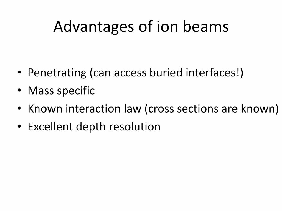
Advantages of ion beams*
• Penetrating (can access buried interfaces!)
• Mass specific
• Known interaction law (cross sections are known)
• Excellent depth resolution
*Mostly high and medium energy beams
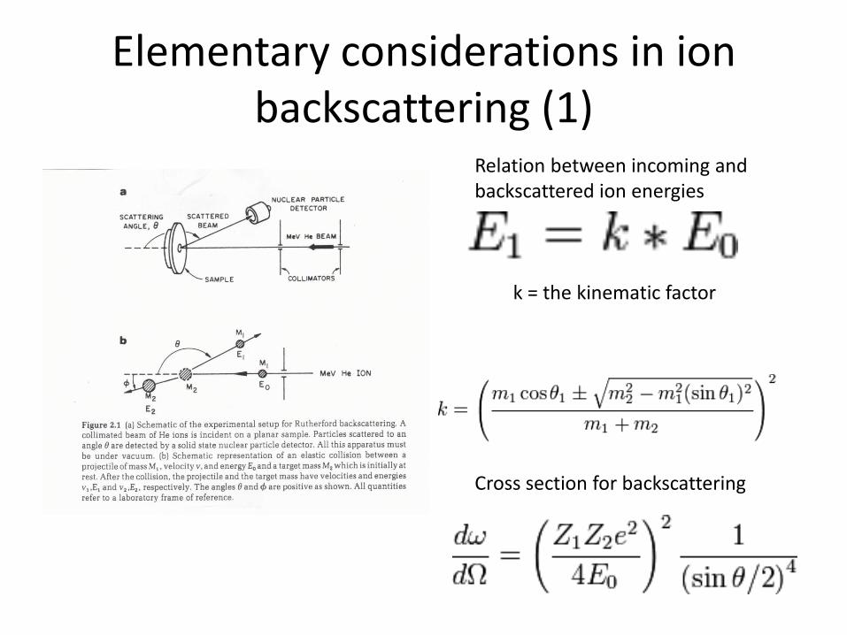
Elementary considerations in ion backscattering (1)
k = the kinematic factor
Relation between incoming and backscattered ion energies
Cross section for backscattering

Elementary considerations in ion backscattering (2)
Depth profiling

Structural work using Medium Energy Ion Scattering (MEIS)

8
MEIS lab at Rutgers
ALD XPS
XPS
IR
NRP
MEIS

Electrostatic ion detector
9 Angle
Ener
gy
~20°
• Depth resolution of ~3 Å near surface • Angular resolution 0.2° • Mass-sensitive: E = E(M, θ) • Quantitative (cross sections are known)
Al
18O
16O

Surface structure and dynamics
N
i i
i
calc
i
Y
YY
NR
1
2
exp
exp1
100
-5 0 5 10 15
-15
-10
-5
0
50.6000
0.8200
1.040
1.260
1.480
1.700
1.920
2.140
2.360
2.580
2.800
3.020
3.240
3.400(a)
d
12 (
%)
d23
(%)
blocking cone
shadow cone
Monte Carlo simulation in the
binary-encounter approximation
Input:
• individual atomic positions
• anisotropic rms vibration amplitude
Output:
Δd
12
Δd
23
50 60 70 80 90 1001101201302
4
6
8
10
[211] [110] [011][011][011][101]
II IIII
Yie
ld (
ML)
Scattering angle (deg)


An (oversimplified) picture of the origin of the oscillatory relaxation
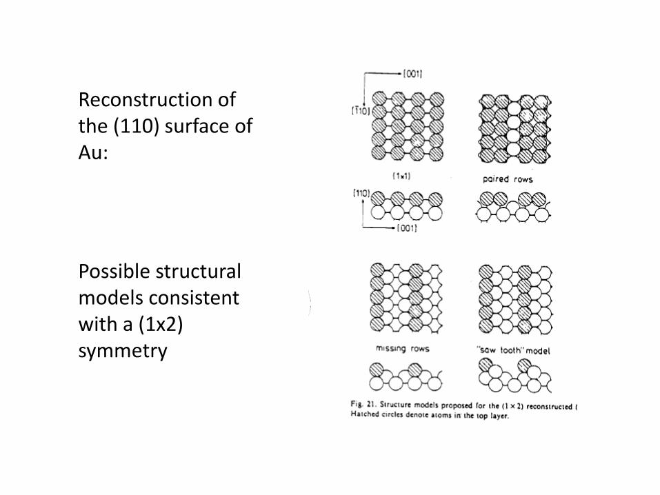
Reconstruction of the (110) surface of Au:
Possible structural models consistent with a (1x2) symmetry


Conclusions:
Missing row structure
Large first layer inwards contraction
Buckling in the lower layers, results in charge density smoothing

Another research example: Surface structure of TiC(001)
Y. Kido et al, PRB 61 1748 (2000)

Sub-nm Depth Resolution from a Materials Perspective:
• Who needs monolayer resolution?
• In this talk, three techniques:
– Elastic Recoil Detection Analysis (ERDA)
– Nuclear Resonance Profiling (NRP)
– Medium Energy Ion Scattering (MEIS)
• Research examples

Gate oxide
Barrier?
Gate
Source Drain Silicon
CMOS Gate Structure
>10nm
The SiO2/Si system: interface
of choice in microelectronics for
40+ years
Moore’s law says that the
gateoxide thickness will soon be
too small (~ 1 nm) due to large
leakage currents from quantum
mechanical tunneling
Motivation for a lot of work in this field today
SiO2 needs to be replaced by a higher dielectric constant material (“high-k”)
Advantages of ion beams
• Penetrating (can access buried interfaces!)
• Mass specific
• Known interaction law (cross sections are known)
• Excellent depth resolution

Medium Energy Ion Scattering (MEIS) - a low-energy, high resolution version of conventional Rutherford Backscattering (RBS)

A comparison between RBS and MEIS
RBS MEIS
Ion energy ~ 2 MeV ~ 100 keV
Detector resolution ~ 15 keV ~0.15 keV
Depth resolution ~ 100 Å ~ 3 Å
2 basic advantages vs. RBS: Often better dE/dx, superior detection equipment
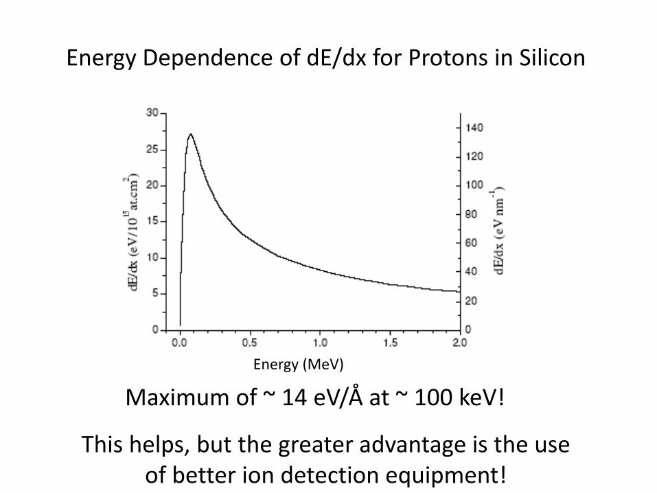
Energy Dependence of dE/dx for Protons in Silicon
Maximum of ~ 14 eV/Å at ~ 100 keV!
This helps, but the greater advantage is the use of better ion detection equipment!
Energy (MeV)

Ion detection equipment
Magnetic
spectrometers
Electrostatic
spectrometers
Kyoto university
(Kimura)
Kobelco
FOM – IBM
(Tromp, van der
Veen, Saris ..)
High Voltage
Engineering
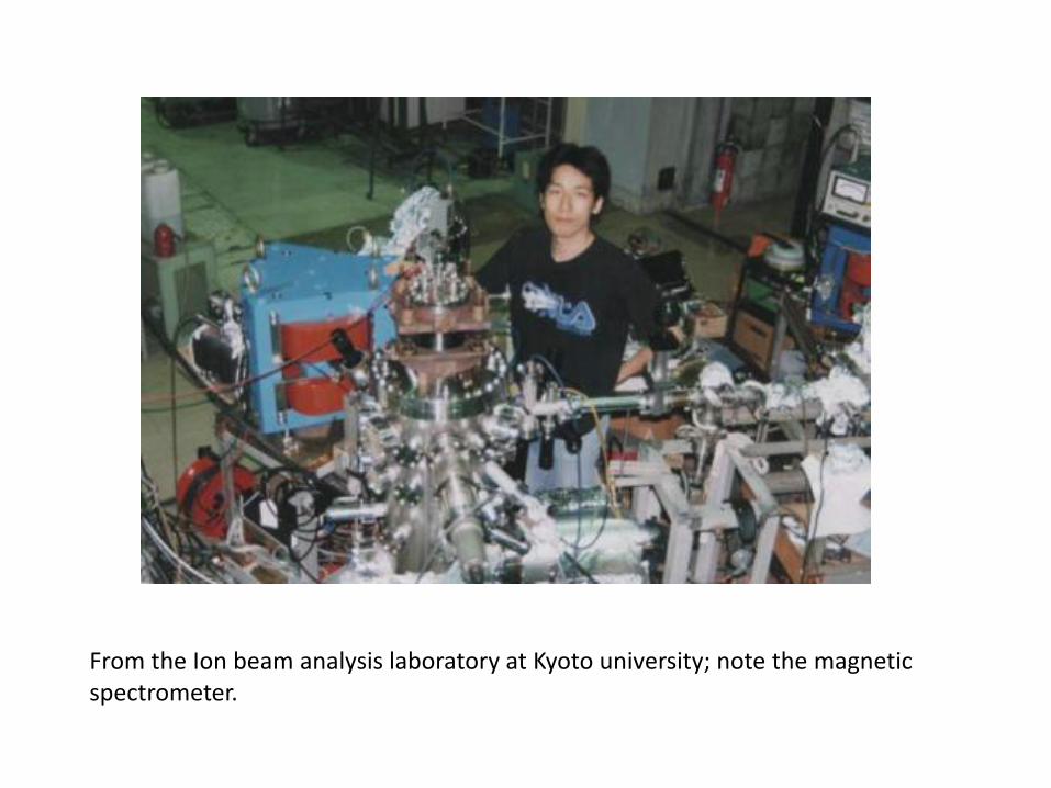
From the Ion beam analysis laboratory at Kyoto university; note the magnetic spectrometer.
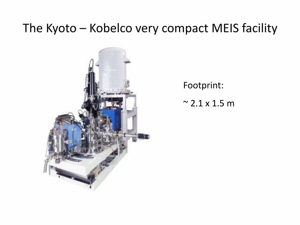
The Kyoto – Kobelco very compact MEIS facility
Footprint:
~ 2.1 x 1.5 m
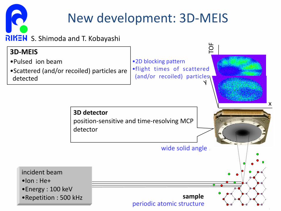
3D-MEIS •Pulsed ion beam
•Scattered (and/or recoiled) particles are detected
periodic atomic structure sample
New development: 3D-MEIS
S. Shimoda and T. Kobayashi
incident beam •Ion : He+ •Energy : 100 keV •Repetition : 500 kHz
x
TOF
wide solid angle
•2D blocking pattern •flight times of scattered (and/or recoiled) particles
3D detector position-sensitive and time-resolving MCP detector

6
4
2
0
-2
-4
42403836343230282624222018Scattered angle 2(°)
[110][331]
f-1 f-2 f-3 f-4
35.3°
Si
22.0°
Angle
fro
m t
he S
i(1
1̄0)
pla
ne (
°)
1 = 67.2° 1 = 62.2° 1 = 57.2° 1 = 52.2°
6
4
2
0
-2
-4
42403836343230282624222018Scattered angle 2(°)
f-1 f-2 f-3 f-4
b-1 b-2 b-3
22.3° 28.8° 39.3°
Er
Angle
fro
m t
he S
i(1
1̄0)
pla
ne (
°)
[011̄1][022̄3][011̄2]
1 = 67.2° 1 = 62.2° 1 = 57.2° 1 = 52.2°
Structural analysis of an Er-silicide on Si(111) substrate using 3D-MEIS
Fig. 3 Structural model of the ErSi2
Cross section cut by the ErSi2(2110) plane
__ Fig.1 3D-MEIS images of the intensities of He particles scattered (a) from Er atoms in the Er-silicide film and (b) from Si atoms in the Si substrate.
Fig. 2 TOF spectra obtained from the data detected in regions indicated by A and B in Fig.1.
(2110) __
A
B
(a)
(b)
S. Shimoda and T. Kobayashi
c
a2a1
B
A
70
60
50
40
30
20
10
0
Inte
nsi
ty (
counts
)
360340320300280260
TOF (ns)
A
B
Er
Si
Er Si
b-1
b-2
b-3
c=0.403nm
b-1 : [0112]
b-2 : [0223]
b-3 : [0111]
_
_
3a=0.665nm

K. Kimura et al. (Kyoto) NIM B99, 472 (1995)
Early High Resolution Work
Sb on Si(100) with caps of varying thickness; some Sb segregates to the surface

Recent Very High Resolution Work
Carstanjen et al. (Stuttgart) (to be published)
Note use of N+ and N2+ ions and charge exchange effects

The Stuttgart high resolution ion analyzer

Determining interface strain using monolayer resolution ion scattering and blocking (Moon et al.)
Ozone oxide, no strain
Thermally grown oxide, significant strain

ZrO
2 (ZrO2)x(SiO2)y
Si(100)
100 keV p+ Backscattered proton
energy spectrum
depth
profile
• Sensitivity: 10+12 atoms/cm2 (Hf, Zr) 10+14 atoms/cm2 (C, N)
• Accuracy for determining total amounts: 5% absolute (Hf, Zr, O), 2% relative 10% absolute (C, N)
• Depth resolution: (need density) 3 Å near surface 8 Å at depth of 40 Å
?
Spectra and information content

Depth resolution for 100 keV protons (resolution of the spectrometer 150 eV)
Stopping power SiO2 12 eV/Å; Si3N4 20 eV/Å; Ta2O5 18 eV/Å
"Near surface" depth resolution 3-5 Å; worse for deeper layers due to energy straggling
Depth resolution and concentration profiling
Layer model:
raw spectrum
5
4
3 2 1
layer numbers
Energy, keV3 Å
H+
SUBSTRATE
Layer 1
Layer 2
Layer 3
….
Layer n
• Areas under each peak
corresponds to the concentration
of the element in a 3Å slab
• Peak shapes and positions come
from energy loss, energy
straggling and instrumental
resolution.
• The sum of the contributions of
the different layers describes the
depth profile.

1. O18 uptake at the surface!
2. Growth at the interface
3. O16 loss at the surface
4. O16 movement at the interface!
Oxygen Isotope Experiments: SiO2 growth mode
Gusev, Lu, Gustafsson, Garfunkel, PRB 52, 1759 (1995)

Schematic model
SiO2
Transition zone,
SiOx
Si (crystalline)
Surface exchange
Growth
Deal and Grove

75 80 85 90 95
0
5
10
15
20 (3)(2)(1)
(1) as deposited film
(2) vacuum anneal at 600 oC
(3) vacuum anneal at 800 oC
no change in
O or Si profiles
minor rearrangement
of La upon annealing
high-K La-Si-O film
yie
ld (
a.u
.)
proton energy (keV)
Annealing up to 800 °C in vacuum shows no significant change in
MEIS spectra.
Surface remains flat by AFM.
Work on high-k films: MEIS spectra of La2SiO5
before and after vacuum anneal

75 80 85 90 95
0
5
10
15
20
25high-K La-Si-O film
(3)
(2)
(1)
(3)
(2)(1)
SiO
surfsurf intint
La
surfint
(1) as deposited film
(2) anneal in air at 400 oC
(3) anneal in air at 800 oC
La diffusionSiO2 growth at 800
oC
yie
ld (
a.u
.)
proton energy (keV)
stoichiometry and thickness
consistent with other analyses
400°C anneal leads to minor
broadening of the La, O and Si
distributions
800°C anneal shows significant
SiO2 growth at interface
La diffusion towards the Si
substrate
La2SiO5 before and after in-air anneal
MOx
Si
MOx
Si
SiO2+MOx + O2
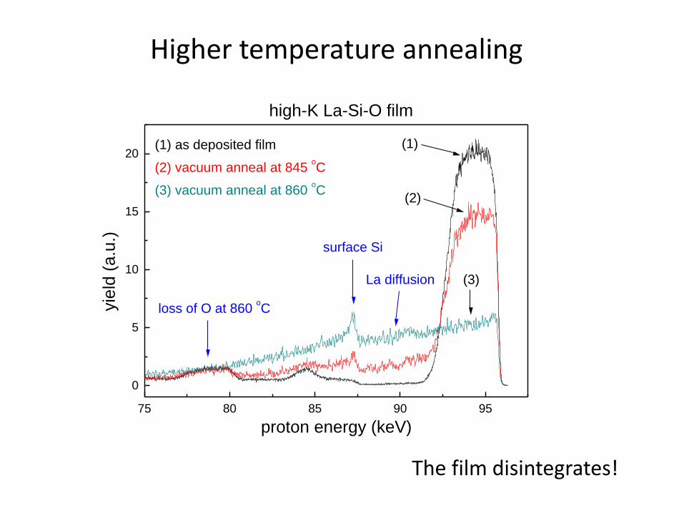
Higher temperature annealing
75 80 85 90 95
0
5
10
15
20
high-K La-Si-O film
(1) as deposited film
(2) vacuum anneal at 845 oC
(3) vacuum anneal at 860 oC
(3)
(2)
(1)
La diffusion
surface Si
loss of O at 860 oC
yie
ld (
a.u
.)
proton energy (keV)
The film disintegrates!

ZrO2 film re-oxidized in 18O2
76 78 80 82 84 86 88 90 92 94 960
100
200
300
400
500
x518
O
16O
Si
Zr
as-deposited film
18
O2 reox. (1 Torr, 500
oC, 5 min)
Yie
ld (
a.u
.)
Proton Energy (keV)
No change in Zr profile
Surface flat by AFM Deeper O and Si
Significant interfacial SiO2 growth for
ZrO2, less for Al2O3
Dramatic oxygen exchange: 18O incorporation and 16O removal
SiO2 growth rate faster than for O2 on Si
Growth faster under ZrO2 than Al2O3
76 78 80 82 84 86 88
0
1
2
3
4
5
6
700 oC
600 oC
500 oC
400 oC
Si interfaceoxygen exchange Al
18O
16O
MEIS spectra of 30 Å Al2O
3 annealed in
3 Torr 18
O2 at 400, 500, 600, 700
oC for 5 min
yie
ld (
a.u
.)
proton energy (keV)
30Å Al2O3 annealed in
3 Torr 18O2
0 200 400 600 800 10000
5
10
15
20
25
30Å ZrO2
30Å Al2O
3
SiO
2 G
row
th (
Å)
O2 Anneal Temp (
oC)
Why GaAs (or Ge)?
• Potentially great advantages over Si-based devices for both high-speed and high-power applications
• The electron mobility of GaAs is 5x that in Si
• Much thinner interfacial oxide

HfO2 on GaAs: MEIS and TEM comparison
No etch
HF etch
*Grazul &
Muller,
Cornell
• TEM and MEIS results are consistent
GaAsa-C
HfO2
Ga-rich oxide
GaAsa-C
HfO2
Ga-rich oxide
TEM* MEIS
O
Hf
O
Hf

TEM of Al2O3 on GaAs
(J. Grazul and D. Muller, Cornell)
HF etch No etch
• no contrast between Al2O3 and GaxAsyO

n(Ga+As), Å-2
n(Al), Å-2
n(O), Å-2
n(O)/n(Al)
HF etch 0.33 1.48 2.23 1.51
No etch 0.55 1.30 2.22 1.70
MEIS data of Al2O3 on GaAs: one-parameter fitting
No etch
HF etch
• interfacial oxide is much thinner
for the HF-etched sample
1.51
1.70
Interfacial oxide: (Ga2O3)0.37(Ga2O)0.63(As2O3)0.17, porous oxide: = 0.5 bulk
80 85 90 95
H+ Energy (keV)
0 10 20 30 40 50 60 700.00
0.01
0.02
0.03
0.04
0.05
Ga
As
Al
O
N (
Å-3)
Depth (Å)
80 85 90 95
H+ Energy (keV)
0 10 20 30 40 50 60 700.00
0.01
0.02
0.03
0.04
0.05
Al
O
N (
Å-3)
Depth (Å)
0 5 10 15 20 25 30
0.85
0.90
0.95
1.00
No
etch
Etched
rms e
rror
Interface thickness (Å)

Epitaxial Oxides
Very versatile materials:
– Small changes in composition → big changes in properties (high-Tc!)
– Combining two different oxides may give multifunctionality and/or entirely new phenomena.
48
Oxides

49
Metallic LaAlO3/SrTiO3 (LAO/STO) interface
LaAlO3 (Eg = 5.8 eV) by PLD or MBE band insulator
SrTiO3 (Eg = 3.2 eV) band insulator
2D Electron Gas
• Metallic conductivity Ohtomo & Hwang, Nature (2004)
• Superconductivity Reyren et al, Science (2007)
• Magnetic order Brinkman et al, Nat. Mat. (2007)
Reyren et al., Science (2007) Brinkman et al., Nat. Mat. (2007) Ohtomo & Hwang, Nature (2004)
T(K)

Origin of metallic state at the interface
50
• Polar catastrophe: polar-nonpolar discontinuity Ohtomo &Hwang, Nature 427 (2004)
This model assumes an abrupt interface

51
Important points
Cationic interdiffusion Nakagawa et al, Nature 5 (2006), Kalabukhov et al, PRL 103 (2009); Willmott et al, PRL 99 (2007).
Oxygen vacancies – have been shown by many to influence carrier concentrations
Conductivity only observed on TiO2 terminated substrates

Samples
• We have investigated samples from three different labs.
• None of the samples were made at Rutgers.
• All made by PLD on TiO2 terminated substrates.
• Post-annealed in oxygen.
• Most data presented today from samples by Prof. H. Hwang, Tokyo (now Stanford).
52

53
He+ channeling spectrum of 4-unit-cell LAO/STO(001)
The measured Sr and Ti peaks fall
at significantly higher ion energies
than those calculated for a sharp
interface:
The energies for the Sr and Ti
peaks are those of both species
present within the outermost u.c.
of LAO outdiffusion of Sr and Ti
to the LAO film
4 u.c. LAO
STO (001)
198.6 KeV He+ [001] [111]
rastering beam
140 150 160 170 180
0
50
100
150
Co
un
ts
He+
Energy [keV]
Experiment
Simulation-no outdiffusion
of Sr and Ti
x4
Sr
Ti
LaTokyo-LO4

54
85 90 95
0
100
200
300
400
500
600
H+ Energy [keV]
Experiment
Simulation-no outdiffusion of Sr and Ti
Yie
ld
Tokyo-MID4 La
SrTi
Al
H+ channeling spectrum of a 4-unit-cell LAO/STO film

55
85 90 95
0
100
200
300
400
500
Experiment
Simulation-no outdiffusion of Sr and Ti
Yie
ld
H+ Energy [keV]
Al
Ti Sr
LaAugsburg
H+ channeling spectrum of a 4-unit-cell LAO/STO film

56
Angle dependent XPS shows poor agreement with sharp interface model (Chambers et al)

57
The LaAlO3/SrTiO3 interface shows evidence for substantial interdiffusion, a useful result for understanding the origin of the many interesting effects shown by this system. More details: Surf. Sci. Rep. 65, 317 (2010)
Conclusions