high resolution pid controller using tapped delay line
DESCRIPTION
Project on High resolution PID controller.TRANSCRIPT
ABSTRACT
Monitoring and controlling of temperature in multi core and many core SOC is an
important criteria in present technology. Thus need for thermal management has
tremendously increased over time. Proportional-Integral-Derivative (PID) controllers is one
such controller for temperature control. It is widely used in automation control systems.
A PID is the most commonly used feedback controller and offers a good solution to many
practical control problems in small as well as large distributed systems.
A 16 bit PID controller using tapped delay line is developed. The controller
parameters are designed using MATLAB/SIMULINK. The circuit under test is a PID
Controller circuit implemented on a low-cost FPGA from XILINX.A multiplierless digital
PID controller is design and implementation on FPGA device. It is more compact, power
efficient and provides high speed capabilities and hardware compatibility for implementing
on FPGA. The proposed method is based on Distributed Arithmetic (DA) architecture which
utilizes less resources.
iii
CONTENTS
Page No
DECLARATION i
ACKNOWLEDGEMENT ii
ABSTRACT iii
LIST OF FIGURES vi
LIST OF TABLES vi
LIST OF ABBREVATIONS vii
CHAPTER 1: INTRODUCTION 1
1.1 Problem statement 2
1.2 Objective of The Project 2
1.3 Applications 2
1.4 Software and hardware used 3
1.5 Organization of The Report 3
CHAPTER 2: LITERATURE SURVEY
2.1 Background 4
2.2 Types of PID Controller 4
2.3 Tunning of PID Controller 7
CHAPTER 3: PROPOSED PID CONTROLLER 8
3.1 Control Terms 9
3.2 Mathematical Analysis 10
3.3 Distributed Arithmetic 13
3.4 Distributed Arithmetic in LUT’s 15
3.5 Tapped Delay Line 16
3.6 Pulse Width Modulation 16
3.7 Peltier Cooler 17
iv

CHAPTER 4: TOOLS USED
4.1 Xilinx ISE 9.2i 19
4.2 Introduction to VHDL 20
4.3 Matlab R2010 a 21
CHAPTER 5: SYNTHESIS OF PID CONTROLLER USING XILINX ISE9.2
5.1 Design Flow 23
5.2 Synthesis Report 24
CHAPTER 6: RTL SCHEMATICS
6.1 RTL Schematic of Top Module 36
6. 2 RTL Schematic of PID Controller 37
6. 3 RTL Schematic of PWM Module 37
6. 4 RTL schematic of proposed PID control with PWM 38
CHAPTER 7: SIMULATIONS AND RESULTS 39
7.1 Hardware Setup and Xilinx XC3S400 Board
40
7.2 Waveforms 41
CHAPTER 8: CONCLUSION AND SCOPE FOR FUTURE WORK 43
REFERENCES 44
APPENDIX A 46
APPENDIX B 53
APPENDIX C 58
v

LIST OF FIGURES
Fig No
Fig.1.1
Titles
Block diagram of sensor and controller
Page No
1
Fig.2.1 Control Loop Employing a PID Control Function 5
Fig.2.2 Block diagram of PID Controller 6
Fig.3.1 Architecture of the Proposed PID Controller 8
Fig.3.2 Distributed Arithmetic with Four Constant Multiplicands 13
Fig.3.3 Four-Bit Multiplication with Constant Coefficient 15
Fig.3.4 Tapped Delay Line 16
Fig.3.5 Input analog signal and a sawtooth waveform 17
Fig.3.6 Peltier cooler module 18
Fig.5.1 synthesis design flow 23
Fig.6.1 Top Module 36
Fig.6.2 PID Controller Module 37
Fig 6.3 PWM Module 37
Fig 6.4 Proposed PID control with PWM module 38
Fig.7.1 Hardware setup and Spartan board 40
Fig.7.2 Simulation result of PID controller 41
Fig.7.3 Simulation results of PWM wave 41
Fig.7.4 Temperature vs Duty cycle curve 42
Fig 7.5 Device summary report of PID controller 42
LIST OF TABLES
Table No. Titles Page No.
3.1 Effects of increasing a given term in a closed-loop system 10
3.2 ROM Table 12
3.3 Module Parameters and Types of Peltier Cooler 18
vi

LIST OF ABBREVATIONS
DA Distributed arithmetic DTDL
Digital Tapped Delay Line
FPGA Field Programmable Gate Array
LUT Look Up Table
NOC Network On Chip
PID Proportional Integral Derivative PWM Pulse Width Modulation
ROM Read Only Memory SOC System On Chip
TEC Thermoelectric Cooler
vii

High Resolution PID Controller Using Tapped Delay Line
INTRODUCTION
CHAPTER 1
More densely packed transistors within the chips are generating more heat per unit area.
Monitoring and controlling the temperature of the chip using digital sensors has the advantages
of having less chip area ,less power consumption and cost effective over analog sensors . The
basic principle block diagram of Digital temperature sensor and control is as shown in figure 1.1.
Figure 1.1: Block diagram of sensor and controller
The principle of temperature sensor is based on the relationship between temperature and
propagation delay of the transistor. Propagation delay of the transistor varies with temperature of
the chip, which is captured by master counter and LUT. Proportional(P), Integral(I) and
Derivative(D) controller is used to maintain the temperature of the die to a setpoint by varying
width of the Pulse Width Modulator signal. The PWM signal changes the direction of current in
Peltier cooler to control the temperature.
M.Tech ( Dept of E&C) 1

High Resolution PID Controller Using Tapped Delay Line
1.1 Problem Statement
Requirement is to design and implement a high Resolution PID Controller using Tapped
delay line for temperature control with less hardware utilization.
1.2 Objective of the Project
In multi core and many core embedded system-on-chip (SoC) millions of transistors are
integrated on a single chip to add more features to the system. In the same way Network on Chip
(NoC) configuration has more number of Intellectual property (IP) cores, which are integrated
and are controlled by a router. In NoC the load is not equally distributed at each part or to each
IP core hence thermal management is more concern in such systems because the heat increases
rapidly where work load is more and it is less at where work load is less. The testing of such
systems through software Built-In-Self-Test (BIST) becomes inconvenient due to its speed
restrictions and more power consumption. Hence the proposed Distributed Temperature Sensor
and Control can be used as hardware Built-In-Self-Test (BIST).The main Objective of this
project is to design and implement a Temperature sensor and control on FPGA. The whole
project is divided into two parts, temperature sensing and temperature controlling. In this report
temperature controlling is discussed using PID Controller. Proportional-Integral-Derivative
(PID) controllers are widely used in automation control systems. A PID is the most commonly
used feedback controller and offers a good solution to many practical control problems in small
as well as large distributed systems. The PID controller compares the measured process value
with a reference setpoint value. The difference or error is then processed to calculate a new
process input, which will try to adjust the measured process value back to the desired setpoint. In
this project we have designed PID controller based on Distributed Arithmetic (DA) architecture
and output of the PID controller is then applied to the Pulse Width Modulator (PWM).PWM
drives the peltier cooler which controls the temperature of the FPGA.
1.3 Applications
Monitoring and controlling the temperature of the chip without using on board temperature
sensor finds its uses in many industrial applications. The demand for small sized, high accuracy
chips has grown over time, and with that, the demand for low consumption smart temperature
M.Tech ( Dept of E&C) 2

High Resolution PID Controller Using Tapped Delay Line
sensors has also grown. The distributed temperature sensor serve as the core circuit for highly
sophisticated temperature sensitive systems like CPU, CCD Cameras.
PID is an important tool for the embedded real-time digital controls designer. The PID is
used extensively in fields such as servo/motor control, robotics, temperature control, and power
electronics. More recently, the PID has been adopted into variant forms that incorporate adaptive
and non-linear controllers.
The major requirement for current applications is low cost, high resolution, and wide
measurement.
1.4 Software and Hardware Used
Xilinx 9.2 is used as VHDL design entry tool, schematic, and also for simulation, synthesis
and implementation. Spartan 3 XC3s400-4pq208 FPGA kit is used as target device for
implementation. Matlab/Simulink is used for tuning of the PID parameters. Peltier cooler to
control the temperature
1.5 Organization of the Report
This dissertation consists of 8 chapters including the present introductory one. Chapter 2
consists of background of PID controller explanation. Chapter 3 explains block diagram and the
architecture of PID controller. Chapter 4 deals with the introductory part of tools used. Chapter 5
explains the program flow, modern developments and the detailed hardware report i.e. Synthesis
Report. Chapter 6 covers the RTL schematics obtained by the Xilinx Synthesis tool. Chapter 7
shows the Simulations Results and the waveforms obtained using different tool. Chapter 8
concludes the dissertation with suggestions for further work.
M.Tech ( Dept of E&C) 3

High Resolution PID Controller Using Tapped Delay Line
2.1 Background
LITERATURE SURVEY
CHAPTER 2
The PID controller enjoys the honor of being the most commonly used dynamic control
technique. Over 85% of all dynamic (low-level) controllers are of the PID variety. The basic idea
is that the controller reads the system state by a sensor. Then it subtracts the measurement from a
desired reference to generate the error value e(t). The error will be managed in three ways, to
handle the present, through the proportional term, recover from the past, using the integral term,
and to anticipate the future, through the derivate term. Early feedback control devices implicitly
or explicitly used the ideas of proportional, integral and derivative action in their structures.
However, it was probably not until Minorsky’s work on ship steering published in 1922, that
rigorous theoretical consideration was given to PID control [5]. This was the first mathematical
treatment of the type of controller that is now used to control almost all industrial processes.
Initially, digital PID controller was designed by using microprocessors or
microcontrollers. This method has a disadvantage in speed of operations because the operations
depend on software which has a sequence of instructions and commands which needs many
machine cycles to execute. [6]
2.2 Types of PID Controller
There are different types of Controllers like On-Off Controller, Proportional controller ,
PID Controller etc, each having its own advantages. An on-off controller is the simplest form of
speed control device. The output from the device is either on or off, with no middle state. An on-
off controller will switch the output only when the speed crosses the setpoint.
Proportional controls are designed to eliminate the cycling associated with on-off control.
A proportional controller decreases the average power supplied to the motor as the speed
approaches setpoint. This proportioning action can be accomplished by turning the output on and
off for short time intervals.
PID controller combines proportional control with two additional adjustments, which
helps the unit automatically compensate for changes in the system. The proportional, integral and
M.Tech ( Dept of E&C) 4
High Resolution PID Controller Using Tapped Delay Line
derivative terms must be individually adjusted or “tuned” to a particular system using trial and
error[14]. It provides the most accurate and stable control of the three controller types, and is
best used in systems which have a relatively small mass, those which react quickly to changes in
the energy added to the process.
Systems that are subject to wide temperature cycling need proportional control.
Depending on the precision required, some processes may require full "PID" control. It provides
the most accurate and stable control of the three controller types, and is best used in systems
which have a relatively small mass, those which react quickly to changes in energy added to the
process. It is recommended in systems where the load changes often, and the controller is
expected to compensate automatically due to frequent changes in setpoint, the amount of energy
available, or the mass to be controlled.
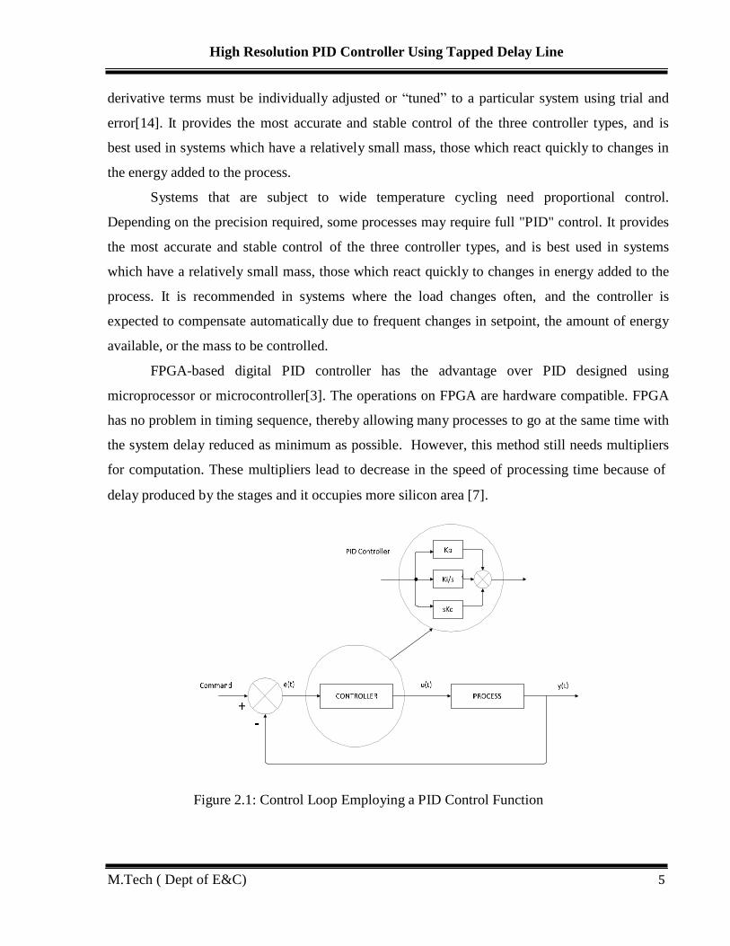
FPGA-based digital PID controller has the advantage over PID designed using
microprocessor or microcontroller[3]. The operations on FPGA are hardware compatible. FPGA
has no problem in timing sequence, thereby allowing many processes to go at the same time with
the system delay reduced as minimum as possible. However, this method still needs multipliers
for computation. These multipliers lead to decrease in the speed of processing time because of
delay produced by the stages and it occupies more silicon area [7].
Figure 2.1: Control Loop Employing a PID Control Function
M.Tech ( Dept of E&C) 5

High Resolution PID Controller Using Tapped Delay Line
For the temperature control application, the desired temperature is called the setpoint
(SP). The input to the process is called the manipulated variable (MV). The difference between
the temperature measurement and the setpoint is the error (e) PID control is useful in systems
where the load is continually varying and the controller is expected to respond automatically to
frequent changes in setpoint—or deviations of the regulated variable. The FPGA-based
controllers offer advantages such as high-speed computation, complex functionality, real-time
processing capabilities and low power. An FPGA chip consists of a lot of memory blocks,
referred to as Look-Up Tables (LUT) [13], which can be utilized to improve performance of
certain operations such as multiplication while the trade-off for speed can be tolerated. In this
project, we study the design of an efficient PID controller using the distributed arithmetic (DA)
scheme. Based on the LUT scheme, the proposed PID controller reduces the cost of the FPGA
design by enabling the chip to accommodate more logic and arithmetic functions while requiring
less power consumption[4][16].
Figure 2.2 : Block diagram of PID Controller
Also, due to the flexibility of using look-up tables in FPGAs. This is due to the fact that
custom-made logic can generally outperform the general purpose microcontrollers [8]. This has
been designed using distributed arithmetic (DA).
M.Tech ( Dept of E&C) 6

High Resolution PID Controller Using Tapped Delay Line
DA hides the explicit multiplications by ROM look-ups hence it reduces the area by 50%
in the hardware design. The excess of temperature on the FPGA is modulated by pulse width
modulation (PWM) whose duty cycle depends on the output of the PID controller. The PWM
signal drives the Peltier cooler which is mounted on the FPGA. Peltier cooler is also known as
thermoelectric cooler (TEC), works on the principle of Peltier effect i.e. whenever current
flows through the peltier cooler (conductor) depending on the change in polarity of the current
flow, the junction of two conductors will either release or absorb heat.
2.3 Tuning a PID (Three-Mode) Controller
Tuning a temperature controller involves setting the proportional, integral, and derivative
values to get the best possible control for a particular process. If the controller does not include
an auto-tune algorithm or the auto-tune algorithm does not provide adequate control for the
particular application, the unit must then be tuned using a trial and error method.
Implementations using a single architecture, shared to perform different PID controllers,
have also been considered [9]. Since with FPGAs we are not constrained to a specific number of
bits to represent data such is the case when using e.g. microcontrollers, the implementation of
PID controllers using FPGAs may permit to use in embedded systems more efficient, robust and
stable controllers and auto-tuning schemes[10].
M.Tech ( Dept of E&C) 7

High Resolution PID Controller Using Tapped Delay Line
PROPOSED PID CONTROLLER
Chapter 3
The PID algorithm, now widely used in industrial process control, has been recognized
and employed for many pneumatic controllers. Fig3.1 shows the architecture of the proposed
PID controller using Tapped delay line.
Figure 3.1: Architecture of the Proposed PID Controller
This has been designed using distributed arithmetic (DA). DA hides the explicit
multiplications by ROM look-ups hence it reduces the area by 50% in the hardware design.
M.Tech ( Dept of E&C) 8
High Resolution PID Controller Using Tapped Delay Line
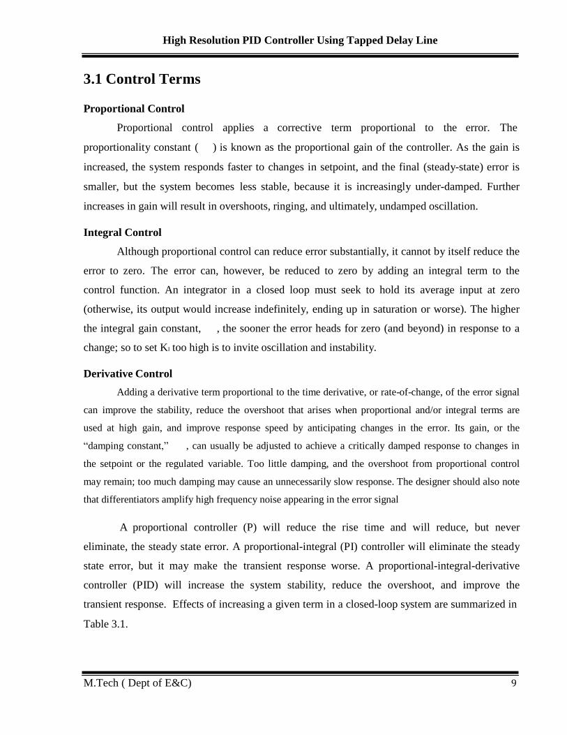
3.1 Control Terms
Proportional Control
Proportional control applies a corrective term proportional to the error. The
proportionality constant ( ) is known as the proportional gain of the controller. As the gain is
increased, the system responds faster to changes in setpoint, and the final (steady-state) error is
smaller, but the system becomes less stable, because it is increasingly under-damped. Further
increases in gain will result in overshoots, ringing, and ultimately, undamped oscillation.
Integral Control
Although proportional control can reduce error substantially, it cannot by itself reduce the
error to zero. The error can, however, be reduced to zero by adding an integral term to the
control function. An integrator in a closed loop must seek to hold its average input at zero
(otherwise, its output would increase indefinitely, ending up in saturation or worse). The higher
the integral gain constant, , the sooner the error heads for zero (and beyond) in response to a
change; so to set KI too high is to invite oscillation and instability.
Derivative Control
Adding a derivative term proportional to the time derivative, or rate-of-change, of the error signal
can improve the stability, reduce the overshoot that arises when proportional and/or integral terms are
used at high gain, and improve response speed by anticipating changes in the error. Its gain, or the
“damping constant,” , can usually be adjusted to achieve a critically damped response to changes in
the setpoint or the regulated variable. Too little damping, and the overshoot from proportional control
may remain; too much damping may cause an unnecessarily slow response. The designer should also note
that differentiators amplify high frequency noise appearing in the error signal
A proportional controller (P) will reduce the rise time and will reduce, but never
eliminate, the steady state error. A proportional-integral (PI) controller will eliminate the steady
state error, but it may make the transient response worse. A proportional-integral-derivative
controller (PID) will increase the system stability, reduce the overshoot, and improve the
transient response. Effects of increasing a given term in a closed-loop system are summarized in
Table 3.1.
M.Tech ( Dept of E&C) 9

High Resolution PID Controller Using Tapped Delay Line
Table 3.1 : Effects of increasing a given term in a closed-loop system
Gain
Constant
Rise
Time
Overshoot Settling
Time
Steady State
Error
Kp Decreases Increases Little Change Decreases
Ki Decreases Increases Increases Eliminate
Kd Little Change Decreases Decreases Little Change
3.2 Mathematical Analysis
The analytical equation of PID controller is given by
U(t) = + ∫edt + (de/dt) + PI(0) (3.1)
Where,
Kp = proportional gain
Kd = derivative gain
e = error in % of full scale range
Ki = integral gain
PI(0) = value of integral term at t=0
U(t) is the control signal and e is the control error .The reference value is also called the
setpoint. The control signal is thus a sum of three terms: the P-term (which is proportional to the
error), the I-term (which is proportional to the integral of the error), and the D term (which is
proportional to the derivative of the error). The controller parameters are proportional gain
integral gain and derivative gain . The controller can also be parameterized as
= + +
(3.2)
where is called integral time and derivative time. The proportional part acts on the
present value of the error, the integral represent and average of past errors and the derivative can
be interpreted as a prediction of future errors based on linear extrapolation.
M.Tech ( Dept of E&C) 10

$
High Resolution PID Controller Using Tapped Delay Line
Laplace transform of equation (3.1) will result in,
= + + (3.3)
Also the transfer function of PID controller is
= + + (3.4)
Where, D(S) is transfer of PID controller.
Transforming equation (3.4) into digital domain gives the transfer function of digital PID
controller.
!
!
= + " + (3.5)
Equation (3.5) can be realized to,
= # ! ! % $ &
(3.6)
# !' $ !'
$ &
And the coefficients () , (* and (+ can be given as
= +
+
(3.7)
= − +
−
(3.8)
% =
(3.9)
Where , and are proportional, integral and derivative parameters respectively
of digital PID controller and T is sampling period.
Taking Inverse z- transform of equation (3.7) and deriving it into difference equation it will give:
- ' = - ' − + ' + ' − + % ' − (3.10)
M.Tech ( Dept of E&C) 11
High Resolution PID Controller Using Tapped Delay Line
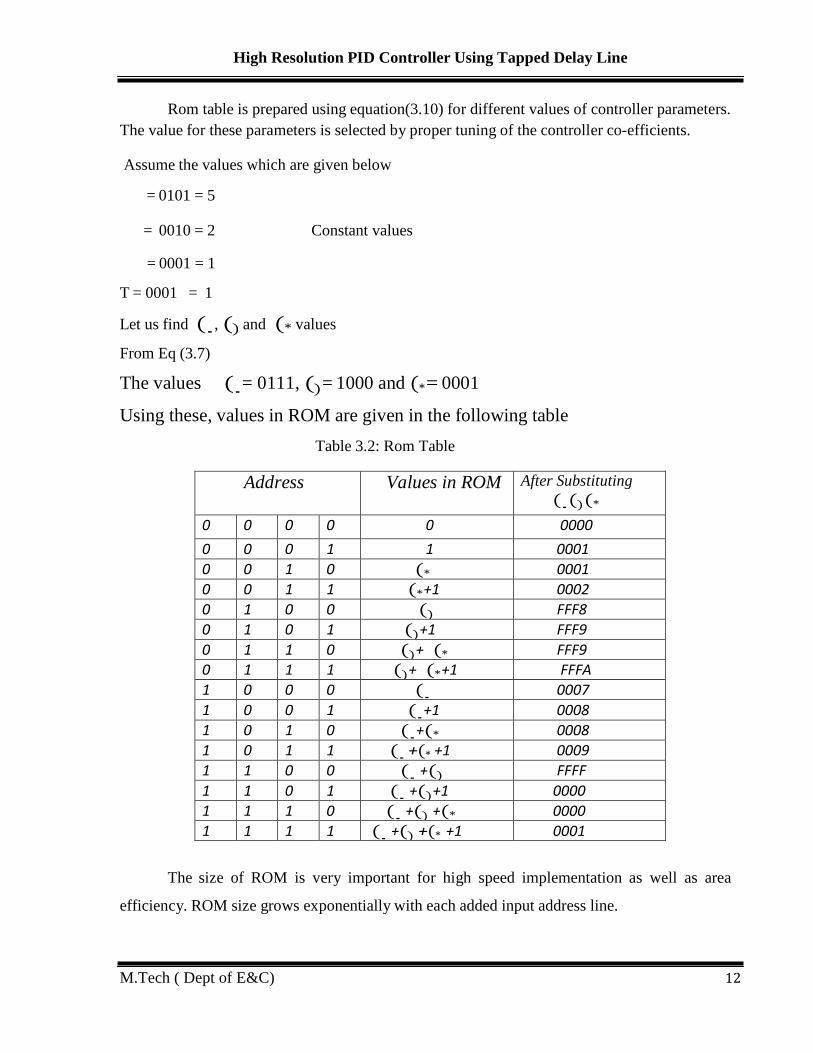
Rom table is prepared using equation(3.10) for different values of controller parameters.
The value for these parameters is selected by proper tuning of the controller co-efficients.
Assume the values which are given below
= 0101 = 5 = 0010 = 2 Constant values
= 0001 = 1
T = 0001 = 1
Let us find (., () and (* values
From Eq (3.7)
The values (.= 0111, () = 1000 and (*= 0001
Using these, values in ROM are given in the following table
Table 3.2: Rom Table
Address Values in ROM After Substituting
(. () (*
0 0 0 0 0 0000
0 0 0 1 1 0001
0 0 1 0 (* 0001
0 0 1 1 (* +1 0002
0 1 0 0 () FFF8
0 1 0 1 () +1 FFF9
0 1 1 0 () + (* FFF9
0 1 1 1 () + (* +1 FFFA
1 0 0 0 (. 0007
1 0 0 1 (. +1 0008
1 0 1 0 (. +(* 0008
1 0 1 1 (. +(* +1 0009
1 1 0 0 (. +() FFFF
1 1 0 1 (. +() +1 0000
1 1 1 0 (. +() +(* 0000
1 1 1 1 (. +() +(* +1 0001
The size of ROM is very important for high speed implementation as well as area
efficiency. ROM size grows exponentially with each added input address line.
M.Tech ( Dept of E&C) 12

High Resolution PID Controller Using Tapped Delay Line
3.3 Distributed Arithmetic
Distributed arithmetic is a method of performing multiplication by distributing the
operation over many LUTs. Figure 3.2 shows a four product MAC function that uses sequential
shift and add to multiply four pairs, and then sums their partial product to obtain a final result.
Each multiplier forms partial products by multiplying the multiplicand by one bit of the input
data (multiplier) at a time, using an AND gate.
Figure 3.2: Distributed Arithmetic with Four Constant Multiplicands
The multiplierless distributed arithmetic (DA)-based technique has gained substantial
popularity, due to its high-throughput processing capability and increased regularity, results in
cost-effective and area-time efficient computing structures. The main operations required for
DA-based computation of inner product are a sequence of lookup table (LUT) accesses followed
by shift accumulation operations of the LUT output. DA-based computation is well suited for
FPGA realization, because the LUT as well as the shift-add operations, can be efficiently
mapped to the LUT-based FPGA logic structures.
At the end of the process, each partial product result of each input bit is summed prior to
the final scaling accumulator stage, which performs a shift-accumulate. The distributed-
M.Tech ( Dept of E&C) 13

High Resolution PID Controller Using Tapped Delay Line
arithmetic circuit simultaneously performs four multiplications and sums the results when all of
the products are completed. The scaling accumulator shifts the sums of partial products
according to the appropriate number of bits and accumulates the result to provide the final
multiplier output.
Consider the following Eq (3.11) inner product of two M dimensional vectors K and 0,
where K is a constant vector, 0 is the input sample vector, and 1 is the result.
4"
1 = 2 3 03 %.
35
Using B-bit 2's complement binary representation scaled such that |03 | < 1 produces
8"
03 = −73 + 2 73'
"' %.
'5
Where 73' are the bits (0 or 1) of 03 , 73 is the most significant bit, and 73 (8− ) is the least
significant bit. Thus
4" 8"
1 = 2 3 9−73 + 2 73' "' : %. %
35 '5
by rearranging summation terms
4" 8" ;"
1 = 2 3 73 + 2 92 3 73' : "' %. <
35 '5 35
The computation in distributed arithmetic is represented by Eq (3.14) shown above. The
values of 73' are either 0 or 1, resulting in bracketed term having only ' possible values. Since
K is a constant vector, the bracketed term can be Pre computed and stored in memory using
either lookup table (LUT) or ROM. The lookup table is then addressed using the individual bits
of input samples, 0 with the final result y computed after B cycles, regardless of lengths of
vectors K and 0. This leads to a multiplier less realization of vector multiplication.
M.Tech ( Dept of E&C) 14
High Resolution PID Controller Using Tapped Delay Line
3.4 Distributed Arithmetic in LUTs
Figure 3.3 shows how to implement distributed arithmetic using LUTs. The combined
product and adder tree are reduced for the LUT implementation. LUT contains the sums of
constant coefficients for all possible input combinations to the LUT. The sums of the bits from
the LUTs are added together in the scaling accumulator and shifted by the appropriate weights.
Figure 3.3: Four-Bit Multiplication with Constant Coefficients
Steps to be followed for the computation of inner product using Distributed Arithmetic:
1. Depending on the length of inner product, store all pre-computed partial products in LUT (ex:
if M=3, 2+ =8 partial products should be stored).
2. Use LSB of all inputs as address, to get partial product from LUT.
3. All inputs are right shifted to get the new address and corresponding partial product from
LUT.
4. The partial product obtained in step 1 is right shifted and added with partial product obtained
in step 2 and store the result in register.
5. Repeat the step 2 to get new partial product which is added with right shifted value of register
and store the result in same register. Repeat step 4 until MSB of inputs reaches LSB position.
6. Use LSB of all inputs as address to get partial product from LUT which is subtracted with
right shifted value of register and store the result in same register which gives inner product.
M.Tech ( Dept of E&C) 15

High Resolution PID Controller Using Tapped Delay Line
3.5 Tapped Delay Line
New digital tapped delay line (DTDL) systems have been designed and demonstrated
which leverage low cost FPGA and data converter technology. A tap refers to the extraction of
the signal at a certain position within the delay-line. Fig 3.4 shows a tapped delay line for a delay
of M1 samples. The tap may be interpolating or non-interpolating, and also may be scaled and
implements a shorter delay line within a larger one. Digital methods mainly use tapped delay line
configurations such as Vernier delay line. Vernier Delay Line is one of the digital method to
achieve nanosecond resolution by using a Vernier method. Two delay element chains are used in
Vernier Delay Line. The delay time Tds of delay element in lower delay chain is greater than that
Tdf in upper delay chain
Figure 3.4: A delay line tapped after a delay of M1 samples.
3.6 Pulse Width Modulator (PWM)
Pulse-width modulation (PWM), or pulse-duration modulation (PDM), is a commonly
used technique for controlling power to inertial electrical devices, made
electronic power switches.
practical by modern
The PWM signal is a signal that is either high or low with no intermediate values. The
average value of voltage (and current) fed to the load is controlled by turning the switch between
supply and load on and off
at a fast pace. The longer the switch is on
compared to the off
periods, the higher the power supplied to the load is. The PWM switching frequency has to be
much faster than what would affect the load, which is to say the device that uses the power.
The term duty cycle describes the proportion of 'on' time to the regular interval or 'period'
of time. A low duty cycle corresponds to low power, because the power is off for most of the
time. Duty cycle is expressed in percent, 100% being fully on. The main advantage of PWM is
M.Tech ( Dept of E&C) 16
High Resolution PID Controller Using Tapped Delay Line
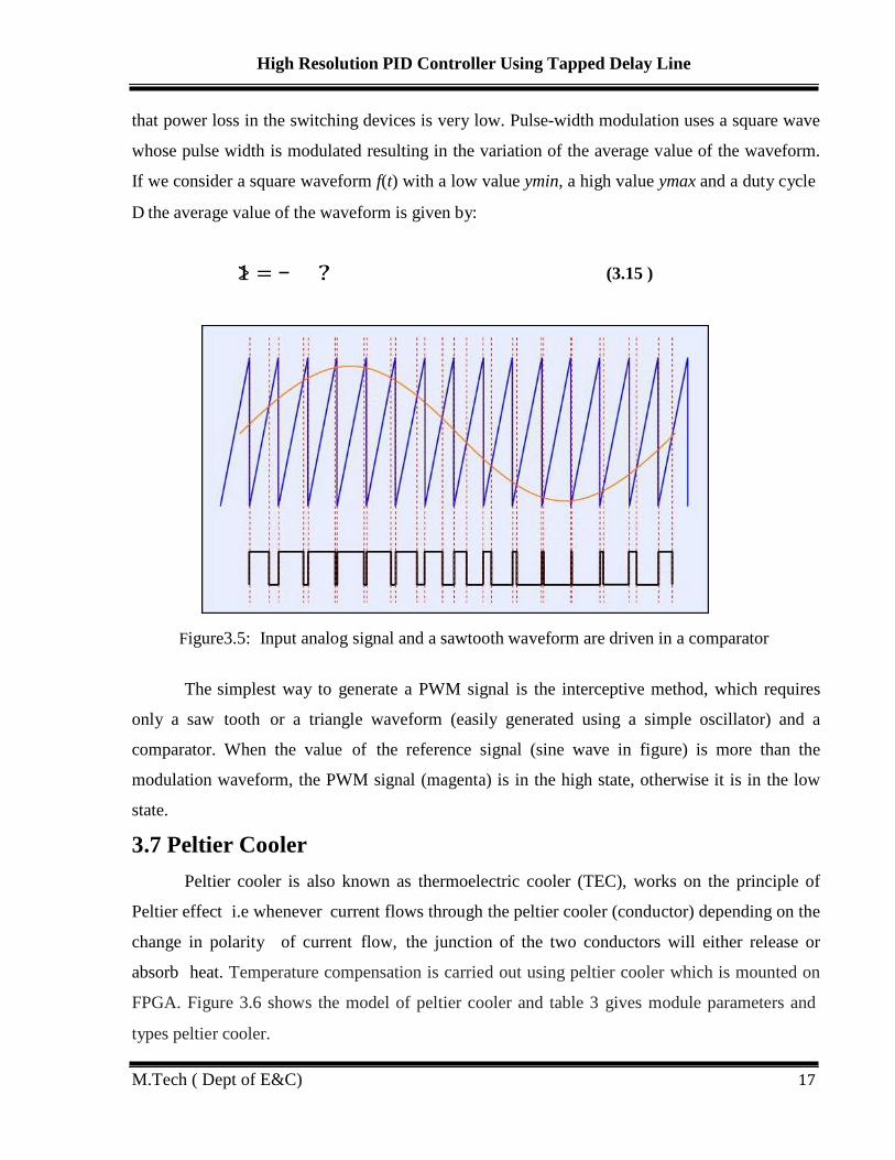
that power loss in the switching devices is very low. Pulse-width modulation uses a square wave
whose pulse width is modulated resulting in the variation of the average value of the waveform.
If we consider a square waveform f(t) with a low value ymin, a high value ymax and a duty cycle
D the average value of the waveform is given by:
1> =
?
(3.15 )
Figure3.5: Input analog signal and a sawtooth waveform are driven in a comparator
The simplest way to generate a PWM signal is the interceptive method, which requires
only a saw tooth or a triangle waveform (easily generated using a simple oscillator) and a
comparator. When the value of the reference signal (sine wave in figure) is more than the
modulation waveform, the PWM signal (magenta) is in the high state, otherwise it is in the low
state.
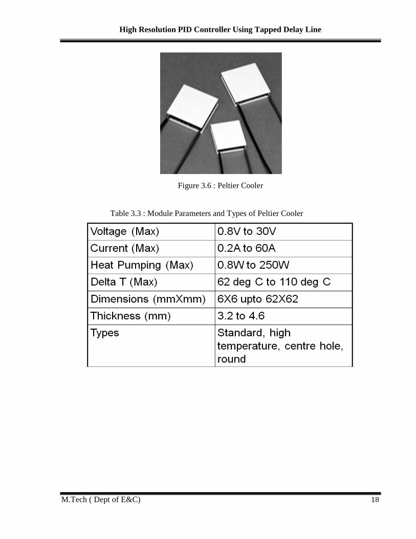
3.7 Peltier Cooler
Peltier cooler is also known as thermoelectric cooler (TEC), works on the principle of
Peltier effect i.e whenever current flows through the peltier cooler (conductor) depending on the
change in polarity of current flow, the junction of the two conductors will either release or
absorb heat. Temperature compensation is carried out using peltier cooler which is mounted on
FPGA. Figure 3.6 shows the model of peltier cooler and table 3 gives module parameters and
types peltier cooler.
M.Tech ( Dept of E&C) 17
High Resolution PID Controller Using Tapped Delay Line
Figure 3.6 : Peltier Cooler
Table 3.3 : Module Parameters and Types of Peltier Cooler
M.Tech ( Dept of E&C) 18

High Resolution PID Controller Using Tapped Delay Line
TOOLS USED
Chapter 4
The tools used for the project are Xilinx ISE 9.2i for writing and synthesizing the VHDL
code, ISE simulator for simulating the code and MATLAB R2010a to test the tuning
functionality of proposed architecture.
4.1 Xilinx ISE 9.2i
Xilinx integrated tool environment is a software tool which enables to write HDL code
and synthesize and optimize to various required user constraints and simulate and implement on
different FPGA and CPLD devices. ISE simulator key features include multi-threaded
compilation, post processing capacity, TCL scriptable GUI and batch mode simulation run and
Standalone waveform viewing capability. It also include debug capabilities like waveform
tracing, waveform viewing, HDL source debugging, power analysis and optimization and
memory editor for viewing and debugging memory elements. There are in-built Xilinx
simulation libraries, so additional mapping or compilation not required.
ISE 9.2i includes new key ease-of-use features to speed engineers through the design
flow faster with easily visible implementation results each step of the way. ISE 9.2i design tools
radically improve utilization of computing resources, providing with greater design flexibility,
enabling to design with higher density FPGAs with widely available 32-bit version of Windows
XP. Improvements in ISE 9.2i design tools permit greater flexibility for designs which leverage
embedded processors. Tighter integration with Xilinx integrated development environment for
embedded design, the Platform Studio, allows embedded users improved access to the design
closure tools residing within the ISE design environment. All versions of ISE design tools
software packages support Windows XP, Windows XP x64, Windows Vista Business, and Linux
Red Hat Enterprise WS.
The standard design flow for Xilinx consists of the following three major steps. The
entire design implementation flow is run simply by selecting the desired result in the Xilinx
graphical User Interface (GUI). The tools automatically determine which programs and files are
needed to bring the appropriate output up to date. M.Tech ( Dept of E&C) 19

High Resolution PID Controller Using Tapped Delay Line
Design Entry and Synthesis
In this step of the design flow, to create the design using a Xilinx-supported schematic
Editor, a Hardware Description Language (HDL) for text based entry or both. Use an HDL for
text-based entry; it must synthesize the HDL file into an industry standard Electronic Data
Interchange Format (EDIF) file. To use the Xilinx Synthesis Technology (XST) tool, a Xilinx –
specific NGC net list file is created, which can be converted to an EDIF file.
Design Implementation
Implementing stage converts the logical design file format, such as EDIF, that is created
in the design entry or synthesis stage into a physical file format. The physical information is
contained in the Native Circuit Description (NCD) file. Then to create a bit stream file from
these files and optionally program a PROM for subsequent programming of the device. Design
Implementation begins with the translating and then mapping of a logical design file to a specific
generation device. It is complete when the physical design is successfully routed and a bit stream
is generated.
Design Verification
Using a gate level simulator, to ensure that the design meets your timing requirements
and functions properly. Verification can be done by simulation which involves testing the design
using software models. It is most effective when testing the functionality of the design and its
performance under worst-case conditions. In circuit verification can be performed by
downloading the design to the device using Xilinx iMPACT Programming software. Design
verification can begin immediately after design entry and can be repeated after various steps of
design implementation.
4.2 Introduction To VHDL
HDL- Hardware Description Language is a computer aided design (CAD) tool for the
modern design and synthesis of digital systems. The recent steady advances in semiconductor
technology continued to increase the power and complexity of digital systems due to their
M.Tech ( Dept of E&C) 20

High Resolution PID Controller Using Tapped Delay Line
complexity, systems cannot be realized using discrete integrated circuits (ICs) they are usually
realized using high density programmable gate arrays (FPGA’s) and require sophisticated CAD
tool. HDL is an integral part of such tools HDL offers the designer a very efficient tool for
implementing and synthesizing designs on chip
The designer uses HDL to describe the system in a computer language that is similar to
several commonly used software languages, such as C. Debugging the design is easy, since HDL
packages implement simulators and test benches. The two widely used hardware description
languages are VHDL and Verilog. Since each language is equally implemented in both academia
and industry [11].
VHDL is acronym for “Very-high-speed-integrated-circuit Hardware Description
Language”. VHDL was introduced as a means to provide a detailed design specification of a
digital circuit, with little thought given to how a circuit might be implemented based on that
specification (the assumption was the requirements in the source file would be captured as a
schematic by a skilled engineer). At the time, the creation of a design specification, although
involved, was almost trivial in comparison to the amount of work required to translate the
specification to a schematic-based structural description needed to fabricate a device. Over
several years, it became clear that a computer program could be written to automatically translate
a VHDL behavioral specification to a structural circuit, and a new class of computer programs
called synthesizers began appearing. A synthesizer produces a low-level, structural description of
a circuit based on its HDL description.
4.3 MATLAB R2010a
MATLAB, which stands for matrix laboratory, is a state-of-the-art mathematical software
package, which is used extensively in both academia and industry. It is an interactive program
for numerical computation and data visualization, which along with its programming capabilities
provides a very useful tool for almost all areas of science and engineering. Unlike other
mathematical packages, such as MAPLE or MATHEMATICA, MATLAB cannot perform
symbolic manipulations without the use of additional toolboxes. It remains however one of the
leading software packages for numerical computation. MATLAB can be used in a wide range of
M.Tech ( Dept of E&C) 21

High Resolution PID Controller Using Tapped Delay Line
applications, including signal and image processing, communications, control design, test and
measurement, financial modelling and analysis, and computational biology.
Simulink is software for modelling, simulating, and analyzing dynamic systems.
Simulink enables you to pose a question about a system, model it, and see what happens. With
Simulink, you can easily build models from scratch, or modify existing models to meet your
needs. Simulink supports linear and nonlinear systems, modelled in continuous time, sampled
time, or a hybrid of the two. Systems can also be multirate — having different parts that are
sampled or updated at different rates. Thousands of scientists and engineers around the world use
Simulink® to model and solve real problems in a variety of industries.
Simulink can use MATLAB to:
• Define model inputs.
• Store model outputs for analysis and visualization.
• Perform functions within a model, through integrated calls to MATLAB
operators and functions.
M.Tech ( Dept of E&C) 22

High Resolution PID Controller Using Tapped Delay Line
Chapter 5
Synthesis Of PID Controller Design Using XILINX ISE 9.2i
5.1 Design Flow
Figure 5.1: Design Flow
M.Tech ( Dept of E&C) 23

High Resolution PID Controller Using Tapped Delay Line
SYNTHESIS:
After validating the RTL model, logic synthesis is performed to map the RTL code to
logic gates in the targeted foundry library. Logic synthesis is the process of automatically
converting a given RTL Hardware Descriptive Language of a design to technology gates; based
on some design constraints. The result of the synthesis process is a net list composed of registers,
combinational logic, interconnects and macro cell instantiations. The tool used in this step is
XILINX ISE 9.2i synthesized net list should be simulated using the same test vectors used to
validate the RTL. In addition, after creating the source files verifies the design’s behavior with
simulation and add constraints. The design is ready to be synthesized and implemented. XILINX
ISE 9.2i Project Navigator) is used for post-simulation purpose. RTL Schematic and Technology
Schematic can be generated and viewed in the synthesizer. Moreover, post-synthesis simulation
will give layout of the design. The design is then Synthesis with XST (default) followed by
translate and mapping. The logic gates of the controller are placed and routed on the CLB’s of
the FPGA. Following PAR, additional verification can be done on the design before creating a
configuration files for downloading to the FPGA. RTL code is synthesized, implementation and
generated bit file using XILINX ISE 9.2i. Then this bit file is loaded into the FPGA.
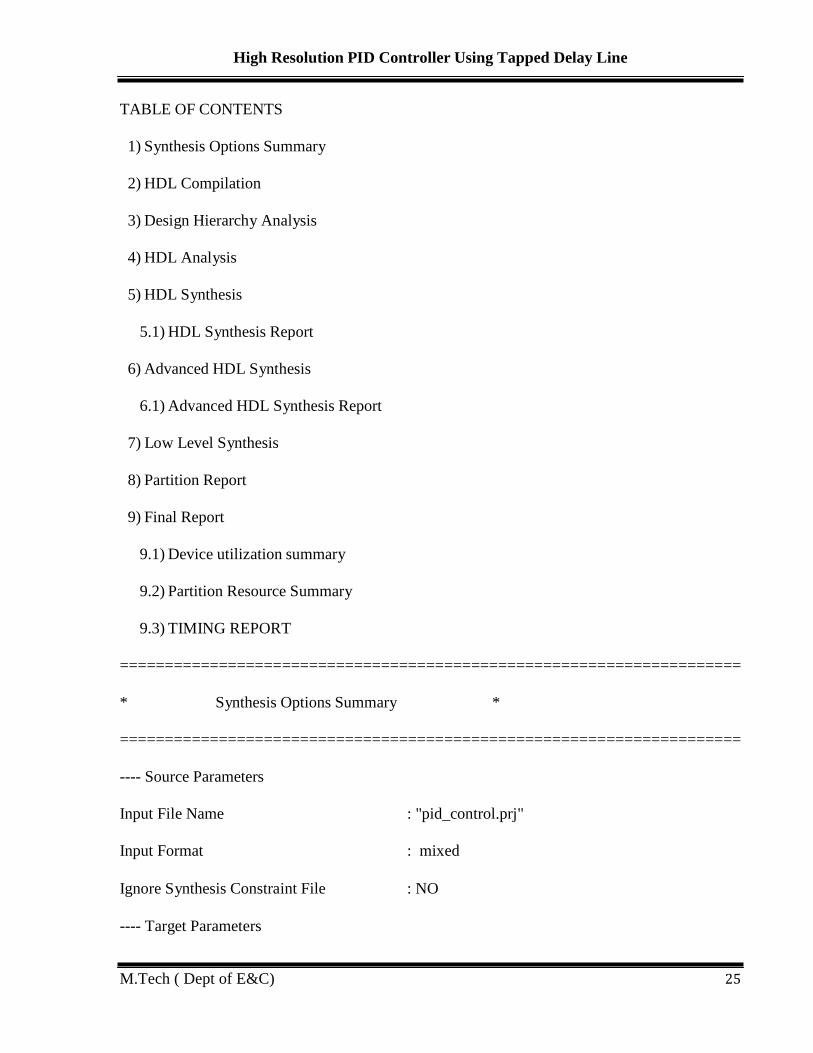
5.2 Synthesis Report Release 9.2i - xst J.30
Copyright (c) 1995-2007 Xilinx, Inc. All rights reserved.
--> Parameter TMPDIR set to ./xst/projnav.tmp
CPU : 0.00 / 0.09 s | Elapsed : 0.00 / 0.00 s
--> Parameter xsthdpdir set to ./xst
CPU : 0.00 / 0.09 s | Elapsed : 0.00 / 0.00 s
--> Reading design: pid_control.prj
M.Tech ( Dept of E&C) 24
High Resolution PID Controller Using Tapped Delay Line
TABLE OF CONTENTS
1) Synthesis Options Summary
2) HDL Compilation
3) Design Hierarchy Analysis
4) HDL Analysis
5) HDL Synthesis
5.1) HDL Synthesis Report
6) Advanced HDL Synthesis
6.1) Advanced HDL Synthesis Report
7) Low Level Synthesis
8) Partition Report
9) Final Report
9.1) Device utilization summary
9.2) Partition Resource Summary
9.3) TIMING REPORT
=====================================================================
* Synthesis Options Summary *
=====================================================================
---- Source Parameters
Input File Name : "pid_control.prj"
Input Format : mixed
Ignore Synthesis Constraint File : NO
---- Target Parameters
M.Tech ( Dept of E&C) 25
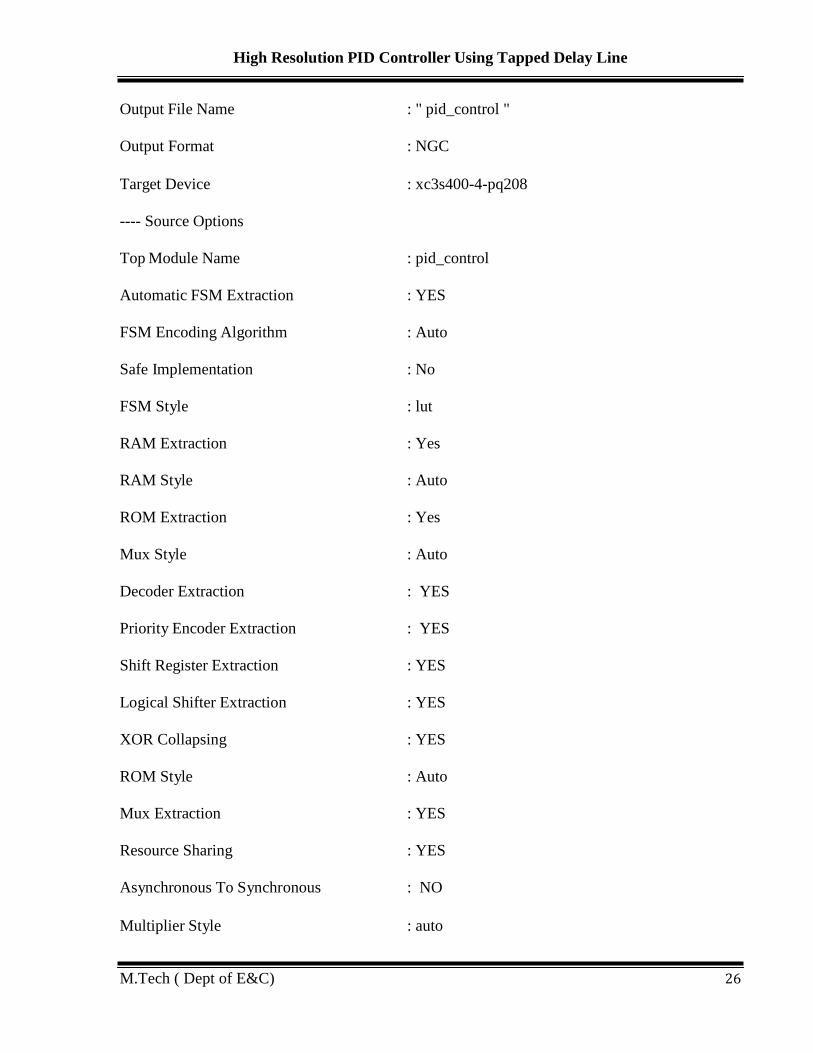
High Resolution PID Controller Using Tapped Delay Line
Output File Name : " pid_control "
Output Format : NGC
Target Device : xc3s400-4-pq208
---- Source Options
Top Module Name : pid_control
Automatic FSM Extraction : YES
FSM Encoding Algorithm : Auto
Safe Implementation : No
FSM Style : lut
RAM Extraction : Yes
RAM Style : Auto
ROM Extraction : Yes
Mux Style : Auto
Decoder Extraction : YES
Priority Encoder Extraction : YES
Shift Register Extraction : YES
Logical Shifter Extraction : YES
XOR Collapsing : YES
ROM Style : Auto
Mux Extraction : YES
Resource Sharing : YES
Asynchronous To Synchronous : NO
Multiplier Style : auto
M.Tech ( Dept of E&C) 26

High Resolution PID Controller Using Tapped Delay Line
Automatic Register Balancing : No
---- Target Options
Add IO Buffers : YES
Global Maximum Fan out : 500
Add Generic Clock Buffer(BUFG) : 8
Register Duplication : YES
Slice Packing : YES
Optimize Instantiated Primitives : NO
Use Clock Enable : Yes
Use Synchronous Set : Yes
Use Synchronous Reset : Yes
Pack IO Registers into IOBs : auto
Equivalent register Removal : YES
---- General Options
Optimization Goal : Speed
Optimization Effor : 1
Library Search Order : pid_control.lso
Keep Hierarchy : NO
RTL Output : Yes
Global Optimization : All Clock Nets
Read Cores : YES
Write Timing Constraints : NO
Cross Clock Analysis : NO
M.Tech ( Dept of E&C) 27

High Resolution PID Controller Using Tapped Delay Line
Hierarchy Separator : /
Bus Delimiter : <>
Case Specifier : maintain
Slice Utilization Ratio : 100
BRAM Utilization Ratio : 100
Verilog 2000 : YES
Auto BRAM Packing : NO
Slice Utilization Ratio Delta : 5
=====================================================================
HDL Synthesis Report
Macro Statistics
# ROMs : 1
16x16-bit ROM : 1
# Adders/Subtractor : 5
15-bit adder : 1
15-bit subtractor : 2
16-bit adder : 1
16-bit subtractor : 1
# Counters : 1
16-bit up counter : 1
# Registers : 53
1-bit register : 49
16-bit register : 4
M.Tech ( Dept of E&C) 28
High Resolution PID Controller Using Tapped Delay Line
# Comparators : 3
15-bit comparator greater : 1
15-bit comparator less : 1
16-bit comparator greater : 1
=====================================================================
* Advanced HDL Synthesis *
=====================================================================
Loading device for application Rf_Device from file '3s400.nph' in environment C:\Xilinx92i.
INFO:Xst:2506 - Unit <rom> : In order to maximize performance and save block RAM
resources, the small ROM <Mrom_d_mux0000> will be implemented on LUT. If you want to
force its implementation on block, use option/constraint rom_style.
=====================================================================
Advanced HDL Synthesis Report
Macro Statistics
# ROMs : 1
16x16-bit ROM : 1
# Adders/Subtractors : 5
15-bit adder : 1
15-bit subtractor : 2
16-bit adder : 1
16-bit subtractor : 1
# Counters : 1
1 6-bit up counter : 1
M.Tech ( Dept of E&C) 29

High Resolution PID Controller Using Tapped Delay Line
# Registers : 115
Flip-Flops : 115
# Comparators : 3
15-bit comparator greater : 1
15-bit comparator less : 1
16-bit comparator greater : 1
=====================================================================
Final Register Report
Macro Statistics
# Registers : 120
Flip-Flops : 120
=====================================================================
* Final Report *
=====================================================================
Final Results
RTL Top Level Output File Name : pid_control.ngr
Top Level Output File Name : pid_control
Output Format : NGC
Optimization Goal : Speed
Keep Hierarchy : NO
Design Statistics
# IOs : 36
M.Tech ( Dept of E&C) 30

High Resolution PID Controller Using Tapped Delay Line
Cell Usage :
# BELS : 443
# GND : 1
# INV : 46
# LUT1 : 41
# LUT2 : 72
# LUT3 : 33
# LUT4 : 22
# LUT4_D : 2
# LUT4_L : 2
# MUXCY : 133
# VCC : 1
# XORCY : 90 # FlipFlops/Latches : 120
# FD : 36
# FDE : 17
# FDR : 51
# FDS : 16
# Clock Buffers : 1
# BUFGP : 1
# IO Buffers : 35
# IBUF : 34
# OBUF : 1
=====================================================================
M.Tech ( Dept of E&C) 31

High Resolution PID Controller Using Tapped Delay Line
Device utilization summary:
---------------------------
Selected Device : 3s400pq208-4
Number of Slices:
143
out of
3584
3%
Number of Slice Flip Flops:
120
out of
7168
1%
Number of 4 input LUTs:
218
out of
7168
3%
Number of IOs:
36
Number of bonded IOBs: 36 out of 141 25%
Number of GCLKs: 1 out of 8 12%
---------------------------
Partition Resource Summary:
---------------------------
No Partitions were found in this design.
=====================================================================
TIMING REPORT
NOTE: THESE TIMING NUMBERS ARE ONLY A SYNTHESIS ESTIMATE.
FOR ACCURATE TIMING INFORMATION PLEASE REFER TO THE TRACE REPORT
GENERATED AFTER PLACE-and-ROUTE.
Clock Information:
-----------------------------------+------------------------+-------+
Clock Signal | Clock buffer(FF name) | Load |
-----------------------------------+------------------------+-------+
Clk | BUFGP | 120 |
M.Tech ( Dept of E&C) 32
High Resolution PID Controller Using Tapped Delay Line
-----------------------------------+------------------------+-------+
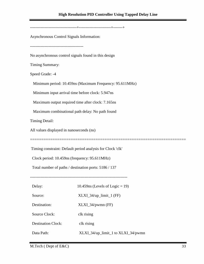
Asynchronous Control Signals Information:
----------------------------------------
No asynchronous control signals found in this design
Timing Summary:
Speed Grade: -4
Minimum period: 10.459ns (Maximum Frequency: 95.611MHz)
Minimum input arrival time before clock: 5.947ns
Maximum output required time after clock: 7.165ns
Maximum combinational path delay: No path found
Timing Detail:
All values displayed in nanoseconds (ns)
=====================================================================
Timing constraint: Default period analysis for Clock 'clk'
Clock period: 10.459ns (frequency: 95.611MHz)
Total number of paths / destination ports: 5186 / 137
-------------------------------------------------------------------------
Delay: 10.459ns (Levels of Logic = 19)
Source: XLXI_34/up_limit_1 (FF)
Destination: XLXI_34/pwmn (FF)
Source Clock: clk rising
Destination Clock: clk rising
Data Path: XLXI_34/up_limit_1 to XLXI_34/pwmn
M.Tech ( Dept of E&C) 33

High Resolution PID Controller Using Tapped Delay Line
Gate Net
Cell:in->out fanout Delay Delay Logical Name (Net Name)
---------------------------------------- ------------
Total 10.459ns (6.374ns logic, 4.085ns route)
(60.9% logic, 39.1% route)
=====================================================================
Timing constraint: Default OFFSET IN BEFORE for Clock 'clk'
Total number of paths / destination ports: 492 / 116
-------------------------------------------------------------------------
Offset: 5.947ns (Levels of Logic = 2)
Source: rst (PAD)
Destination: XLXI_34/up_limit_15 (FF)
Destination Clock: clk rising
Data Path: rst to XLXI_34/up_limit_15
Gate Net
Cell:in->out fanout Delay Delay Logical Name (Net Name)
---------------------------------------- ------------
IBUF:I->O 53 0.821 2.312 rst_IBUF (rst_IBUF)
LUT4:I0->O 16 0.551 1.237 XLXI_34/up_limit_or000094
(XLXI_34/up_limit_or0000)
FDR:R 1.026 XLXI_34/up_limit_0
----------------------------------------
Total 5.947ns (2.398ns logic, 3.549ns route)
(40.3% logic, 59.7% route)
M.Tech ( Dept of E&C) 34

Number of errors : 0 ( 0 filtered)
Number of warnings :
0 (
0 filtered)
Number of infos :
1 (
0 filtered)
High Resolution PID Controller Using Tapped Delay Line
=====================================================================
Timing constraint: Default OFFSET OUT AFTER for Clock 'clk'
Total number of paths / destination ports: 1 / 1
-------------------------------------------------------------------------
Offset: 7.165ns (Levels of Logic = 1)
Source: XLXI_34/pwmn (FF)
Destination: pwm_out (PAD)
Source Clock: clk rising
Data Path: XLXI_34/pwmn to pwm_out
Gate Net
Cell:in->out fanout Delay Delay Logical Name (Net Name)
---------------------------------------- ------------
FDR:C->Q 1 0.720 0.801 XLXI_34/pwmn (XLXI_34/pwmn)
OBUF:I->O 5.644 pwm_out_OBUF (pwm_out)
----------------------------------------
Total 7.165ns (6.364ns logic, 0.801ns route)
(88.8% logic, 11.2% route)
=====================================================================
CPU : 4.93 / 5.04 s | Elapsed : 5.00 / 5.00 s
Total memory usage is 180452 kilobytes
M.Tech ( Dept of E&C) 35
High Resolution PID Controller Using Tapped Delay Line
RTL SCHEMATICS
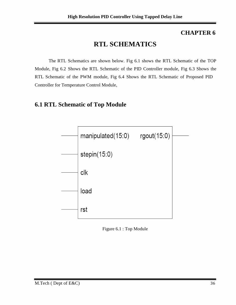
CHAPTER 6
The RTL Schematics are shown below. Fig 6.1 shows the RTL Schematic of the TOP
Module, Fig 6.2 Shows the RTL Schematic of the PID Controller module, Fig 6.3 Shows the
RTL Schematic of the PWM module, Fig 6.4 Shows the RTL Schematic of Proposed PID
Controller for Temperature Control Module,
6.1 RTL Schematic of Top Module
Figure 6.1 : Top Module
M.Tech ( Dept of E&C) 36

High Resolution PID Controller Using Tapped Delay Line
6.2 RTL Synthesis result of PID controller
Figure 6.2 : PID Controller Module
6.3 RTL Synthesis result of PWM Module
Figure 6.3: PWM Module
M.Tech ( Dept of E&C) 37

High Resolution PID Controller Using Tapped Delay Line
6.4 RTL schematic of proposed PID control with PWM
Figure 6.4: Proposed PID control with PWM module
M.Tech ( Dept of E&C) 38
High Resolution PID Controller Using Tapped Delay Line
RESULTS AND SIMULATIONS
Chapter 7
The figure below shows the hardware setup and the waveforms of the proposed PID
controller for temperature control. The fig 7.1 shows the hardware setup of the project, which
shows the Spartan3 Board. The Project is implemented on the Spartan3 board and the results are
displayed on the Seven Segment display. A separate VHDL code is written for the Seven
Segment display. The fig 7.3 shows the simulation result of PID controller and fig 7.4 shows the
simulation result of pwm wave. Fig 7.5 shows the duty cycle of the pwm wave with Temperature
curve. From this curve it is concluded that as the temperature increases the load driving the
FPGA or die must increase the On period to bring back the temperature to normal. The fig 7.6
shows the design device summary of the proposed PID controller.
M.Tech ( Dept of E&C) 39

High Resolution PID Controller Using Tapped Delay Line
7.1 Hardware Setup and Xilinx XC3S400 Board
Figure 7.1 : Hardware setup of the Project
Figure 7.2 : Spartan 3 XC3S400 Board used for Implementation
M.Tech ( Dept of E&C) 40

High Resolution PID Controller Using Tapped Delay Line
7.2 Waveforms
Figure 7.3: Simulation result of PID controller
Figure 7.4: Simulation results of PWM wave
M.Tech ( Dept of E&C) 41

High Resolution PID Controller Using Tapped Delay Line
Figure 7.5 : Temperature vs Duty Cycle curve
Figure 7.6 : Device summary report of PID controller
M.Tech ( Dept of E&C) 42

High Resolution PID Controller Using Tapped Delay Line
Chapter 8
CONCLUSION AND SCOPE FOR FUTURE WORK
PID is implemented using Distributed Arithmetic which reduces the silicon area used by
50%. Also implementing PID controller on FPGA features high processing speed, accuracy,
power, compactness, and cost improvement over other digital implementation techniques and
hardware compatibility for implementing on FPGA. FPGA has another advantage of less design
cycle time for the controller rather than using other methods.
Proposed design is described using VHDL language, simulated using ISE simulator,
synthesized in Xilinx ISE 9.2 tool and implemented on Spartan 3 FPGA kit.
FUTURE SCOPE
Due to the use of Distributed Arithmetic algorithm, the number of PID controllers on
single FPGA chip can be increased immensely.
Co-design Implementation of Controllers
Important and evolving aspect of FPGA based control is the concept of hardware
software co-design using FPGA. in which a microprocessor/ microcontroller is embedded in an
FPGA. Control algorithms that require a large number of computationally involved operations
like matrix manipulations cannot be effectively implemented on a single microprocessor based
set up, as the microprocessor gets bogged down while performing these operations. It is in this
regard that the parallel architecture of the FPGA can be exploited to develop a matrix co-
processor for performing these computations, while the general purpose microprocessor that was
embedded in the chip can be used to perform other operations.
M.Tech ( Dept of E&C) 43
High Resolution PID Controller Using Tapped Delay Line
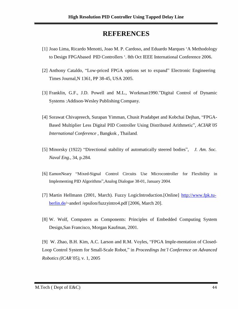
REFERENCES
[1] Joao Lima, Ricardo Menotti, Joao M. P. Cardoso, and Eduardo Marques ‘A Methodology
to Design FPGAbased PID Controllers ‘. 8th Oct IEEE International Conference 2006.
[2] Anthony Cataldo, “Low-priced FPGA options set to expand” Electronic Engineering
Times Journal,N 1361, PP 38-45, USA 2005.
[3] Franklin, G.F., J.D. Powell and M.L., Workman1990.”Digital Control of Dynamic
Systems :Addison-Wesley Publishing Company.
[4] Sorawat Chivapreech, Surapan Yimman, Chusit Pradabpet and Kobchai Dejhan, “FPGA-
Based Multiplier Less Digital PID Controller Using Distributed Arithmetic”, ACIAR’05
International Conference , Bangkok , Thailand.
[5] Minorsky (1922) “Directional stability of automatically steered bodies”, J. Am. Soc.
Naval Eng., 34, p.284.
[6] EamonNeary “Mixed-Signal Control Circuits Use Microcontroller for Flexibility in
Implementing PID Algorithms”,Analog Dialogue 38-01, January 2004.
[7] Martin Hellmann (2001, March). Fuzzy LogicIntroduction.[Online] http://www.fpk.tu-
berlin.de/~anderl /epsilon/fuzzyintro4.pdf [2006, March 20].
[8] W. Wolf, Computers as Components: Principles of Embedded Computing System
Design,San Francisco, Morgan Kaufman, 2001.
[9] W. Zhao, B.H. Kim, A.C. Larson and R.M. Voyles, “FPGA Imple-mentation of Closed-
Loop Control System for Small-Scale Robot,” in Proceedings Int’l Conference on Advanced
Robotics (ICAR’05), v. 1, 2005
M.Tech ( Dept of E&C) 44

High Resolution PID Controller Using Tapped Delay Line
[10] A peled and B. Liu. “A New Hardware Realization of Digital Filters.”
IEEE Trans.ASSP-22, pp.456-462, Dec1974
[11] Charles H Roth, “Jr. Digital System Design Using VHDL”, Brooks/Cole, 1998.
[12] National Instruments: http://www.ni.com. FPGA based control: Millions of transistors at
you command, 2004.
[13] Diligent, Inc., “Diligent Spartan-3 System Board”, June,2004. BOARD-brochure.pdf.
nd
[14] Vikas Gupta, K. Khare and R. P. Singh “Efficient fpga implementation of 2
order digital
controllers using matlab/Simulink”
[15] K.J. Astrom and B. Wittenmark, Computer Controlled Systems, PrenticeHall,
New Jersery,USA 1997
[16] Ian Grout ‘Digital Systems Design with FPGAs and CPLDs’, Elsevier (Newnes press)
publications,2008,chapter-10 ,pp 661-700. © 2009.
M.Tech ( Dept of E&C) 45

High Resolution PID Controller Using Tapped Delay Line
DEVICE DETAILS
APPENDIX A
Spartan-3 trainer Development Board (MXS3MB-0207-003-IM) provides an easy to use
development platform for realizing various designs around SPARTAN-3 FPGA.
Figure A1: Block Diagram
M.Tech ( Dept of E&C) 46

High Resolution PID Controller Using Tapped Delay Line
FEATURES
Figure A.1 shows the SPARTAN-3, which includes the following components and features:
• SPARTAN-3 FPGA: 400 k logic cell SPARTAN -3 FPGA in PQ208 Plastic Quad Flat
Package (MXS3FK-PQ208-IM)
• Three families Spartan 3 /Spartan 3L/Spartan 3 XA.
• Very low cost, high-performance logic solution for high-volume, consumer oriented
applications.
• Densities as high as 74,880 logic cells.
• Three power rails for core (1.2V), I/O’s (1.2V to 3.3V) and Auxiliary purposes (2.5V).
• 326 MHz system clock rate.
• 90 nm process technology. *Select IO™ Signaling.
• Up to 784 I/O pins.
• 622 Mb/s data transfer rate per IO.
• 18 single-ended signal standards. * Logic Resources
• Abundant Logic cells with shift register capability.
• Wide Multiplexers.
• Fast look-ahead carry logic.
• Dedicated 18 x 18 Multipliers. *SelectRAM™ Hierarchical Memory.
• Up to 1,872 Kbits of total block RAM.
• Up to 520 Kbits of Distributed RAM. *Digital Clock Manager (up to 4DCMs)
• Clock skew elimination.
• Frequency synthesis
• High resolution phase shifting.
M.Tech ( Dept of E&C) 47

High Resolution PID Controller Using Tapped Delay Line
* Eight global clock lines and abundant routing.
• Seven Segment Display: Six-character multiplexed seven-segment LED display.
• Serial Interface: One RS-232 channel using MAX3223, 9 pin two channel serial
interfaces.
• DB9 9-pin female connector (DCE connector).
• RS-232 transceiver/level translator using MAX3223 in SSOP package.
• Uses straight-through serial cable to connect to computer or workstation serial port.
• LCD Interface: - 16 Character/ Digit 2 Row LCD.
• Traffic Light Control Interface:-16 green LEDS, 8 Red LEDS, 4 Yellow LEDS.
• Traffic Light Interface module will be connected using 60 pin Connector (J5). * RTC: A Real Time Counter.
* Analog Interface: 12 bit AD7891 ADC and 12 bit AD7541 DAC.
• Analog Input – Eight channels using ADC using AD7891, (500Ksps, 12 bit).
• Analog Output- Two channels using Two DAC’s-AD7541. (12 bit, 100 ns conversion
time)
* DIP Switches: 16 DIP switches. * LEDs: 23 onboard LEDS
• 16 output LEDs (OL 0 – OL 15).
• Done LED.(DONE)
• 6 Power ON LEDs (LED12VN, LED12V, LED5V, LED3.3V, LED2.5V, LED1.2V). * Push Button Switches: 16 momentary-contact push button switches in 4x4 matrix.
* User selectable configuration modes - Boundary scan, Master serial.
* User selectable Interface hardware – Traffic Light, RTC, ADC-DAC.
* Free IOs: 34 pin FRC Connector (J7) provided for free I/Os.
* Clock Oscillator: 4 MHz crystal clock oscillator. Socket for an auxiliary crystal oscillator
clock source.
* JTAG port: JTAG download cable (parallel III) interface.
M.Tech ( Dept of E&C) 48

High Resolution PID Controller Using Tapped Delay Line
* Power Supplies: 5 volts regulated power supply provided along with the board.
• On board 3.3V, 2.5V, 1.2V regulators.
• FPGA supplies viz. Vccint (1.2V) & Vcco (3.3V) are generated on board
Figure A.2 Photograph of Spartan-3 FPGA kit
SEVEN SEGMENT LED DISPLAY
SPARTAN-3 -IM has a Six multiplexed seven segment .Each individual character has a
separate cathode control input. To light an individual signal, drive the individual segment control
signal High along with the associated cathode control signal for the individual character. The
control signal is high, enabling the control inputs for the left-most character. The segment control
inputs, A through G and DP, drive the individual segments that comprise the character. A High
value lights the individual segment, a Low turns off the segment.
M.Tech ( Dept of E&C) 49

High Resolution PID Controller Using Tapped Delay Line
FigureA.3 Seven Segment Display
Types of the seven segment displays Common Cathode Display: In this type of display the cathode of all the LEDs are tied together
and the anode terminals decides the status of the LED, either ON or OFF. To turn ON the LED
i.e. segment value of driven segment should be 1 and 0 for turn OFF.
Figure A.4 Common Cathode Display Common Anode Display: In this type of display all the anode terminals of LEDs are tied
together and the cathode terminals decide the status of the LED either ON or OFF. To turn ON
the LED i.e. segment value of driven segment should be 0 and 1 for turn OFF.
M.Tech ( Dept of E&C) 50

High Resolution PID Controller Using Tapped Delay Line
Figure A.5 Common Anode Display
CONSOLIDATED UCF FOR THE COMPLETE BOARD
Clock and Reset
net "CLK_4M" Loc= "p181";
net "CLK_OPT" Loc= "p180";
net "RESET" Loc= "p182";
Input Switches
net "IL<0>" Loc= "p57";
net "IL<1>" Loc= "p52";
net "IL<2>" Loc= "p51";
net "IL<3>" Loc= "p50";
net "IL<4>" Loc= "p48";
net "IL<5>" Loc= "p46";
net "IL<6>" Loc= "p45";
net "IL<7>" Loc= "p44";
net "IL<8>" Loc= "p43";
net "IL<9>" Loc= "p42";
net "IL<10>" Loc= "p40";
net "IL<11>" Loc= "p39";
net "IL<12>" Loc= "p37";
net "IL<13>" Loc= "p36";
net "IL<14>" Loc= "p35";
net "IL<15>" Loc= "p34";
M.Tech ( Dept of E&C) 51
High Resolution PID Controller Using Tapped Delay Line
Test LEDs
net "OL<0> Loc= "p68";
net "OL<1> Loc= "p67";
net "OL<2> Loc= "p65";
net "OL<3> Loc= "p64";
net "OL<4> Loc= "p63";
net "OL<5> Loc= "p62";
net "OL<6> Loc= "p61";
net "OL<7> Loc= "p58";
net "OL<8> Loc= "p80";
net "OL<9> Loc= "p79";
net "OL<10>" Loc= "p78";
net "OL<11>" Loc= "p77";
net "OL<12>" Loc= "p76";
net "OL<13>" Loc= "p74";
net "OL<14>" Loc= "p72";
net "OL<15>" Loc= "p71";
Display
net "DIS<0>" Loc= "p97";
net "DIS<1>" Loc= "p100";
net "DIS<2>" Loc= "p101";
net "DIS<3>" Loc= "p102";
net "DIS<4>" Loc= "p132";
net "DIS<5>" Loc= "p133";
Seven Segment Interface
net "SEGA" Loc= "p144";
net "SEGB" Loc= "p143";
net "SEGC" Loc= "p141";
net "SEGD" Loc= "p140";
net "SEGE" Loc= "p139";
net "SEGF" Loc= "p138";
net "SEGG" Loc= "p137";
net "SEGDP" Loc= "p135";
M.Tech ( Dept of E&C) 52

High Resolution PID Controller Using Tapped Delay Line
APPENDIX B
Digital Temperature Sensor And Control
Figure B.1 shows the schematic diagram of the digital temperature sensor and control.
PID Controller is used to control the temperature of the device to a required setpoint. In the
below schematic the PID controller is designed using DA arithmetic given in figure 3.1.
Figure B.1: Proposed PID Controller for Temperature Control
The basic digital Temperature Sensor consists of ring oscillator with delay line, counters,
LUTs and display. The delay line is a temperature sensing element, which is made up of
inverters. The xorcy gate is used as a inverter in delay line. There are 109 xorcy gates are used to
get total delay of 250ns. A ring oscillator is a chain of an odd number of XORCY inverter
whose output is connected back to the input.
At normal temperature the frequency of the ring oscillator is close to the on board crystal
clock frequency. As delay
changes with temperature, which alters the
frequency of ring
oscillator. This change is captured by counter which works on the master clock frequency.
M.Tech ( Dept of E&C) 53

High Resolution PID Controller Using Tapped Delay Line
Counters plays an important role in Distributed temperature sensor. There are two
counters are required for the temperature measurement.
1. Master counter
2. Cycle counter
A 20 bit master counter is designed to capture the propagation delay of the ring
oscillator, which works on the rising edge of the on board crystal clock of 4MHz. A 13 bit cycle
counter is used to reduce the no of logic gates in the ring oscillator. The advantage of having
cycle counter in the temperature sensor is, reduced area and better resolution.
The temperature sensing element is made up of 109 XORCY logic gates which are
distributed on FPGA by manually Placing a gate in CLB and routed to cover the entire FPGA.
The seven segment display of the FPGA is used to display the count value which is proportional
to the temperature or by preparing the LUT we can directly display the temperature.
Refresh block reads the counter at regular time interval by enabling the read signal of the
counter.
The count value from the counter output is subtracted with the lower limit of the step
value. The pseudo code for the subtractor is as below.
Pseudo Code For Subtractor:
process(clk)
begin
sub_res1<=step - manp;
if rising_edge(clk) then
temp<= temp+1;
end if;
if (temp="0000000000001110") then
step<="0000011011100100";
sub_res1<=step - manp;
en1<='1';
else
en1<='0';
end if;
M.Tech ( Dept of E&C) 54

High Resolution PID Controller Using Tapped Delay Line
if (temp="0000000000001111") then
en2<='1';
else
en2<='0';
end if;
if (temp="0000000000010000")then
temp<="0000000000000000"
end if;
end process;
sub_res<=sub_res1;
enpwm<=en1;
enpid<=en2;
In this code the manipulated value is subtracted from the step value. The reset signal to
the PID and PWM is generated in the same code. At every 15th
cycle PWM is enabled and at 16th
cycle PID is enabled.
Pseudo Code For PID:
delay_element_16bit XLXI_16 (.clk(clk),
.input1(stepin[15:0]),
.rst(rst),
.output1(XLXN_37[15:0]));
piso1 XLXI_17 (.c(clk),
.clr(rst),
.par_in(XLXN_37[15:0]),
.ups(XLXN_56),
.sload(load),
. ser_out (pisout));
rom XLXI_21 (.a0(piso2out),
.k1(dff2out),
.k2(dff1out),
.k3(pisout),
.clk(clk),
M.Tech ( Dept of E&C) 55

High Resolution PID Controller Using Tapped Delay Line
.d(XLXN_57[15:0]));
accumulator XLXI_22 (.clk(clk),
.clr(rst),
.rom_out(XLXN_57[15:0]),
.q(accout[15:0]));
piso2 XLXI_23 (.c(clk),
.par_in(accout[15:0]),
.ups(XLXN_55),
.load_s(load),
.ser_out(piso2out));
regout XLXI_24 (.clk(clk),
.input1(accout[15:0]),
.rst(rst),
.output1(rgout[15:0]));
GND XLXI_27 (.G(XLXN_56));
GND XLXI_28 (.G(XLXN_55));
FDR XLXI_32 (.C(clk),
.D(dff1out),
.R(rst),
.Q(dff2out));
defparam XLXI_32.INIT = 1'b0;
FDR XLXI_33 (.C(clk),
.D(pisout),
.R(rst),
.Q(dff1out));
defparam XLXI_33.INIT = 1'b0;
The above code is a pseudo code of PID controller using distributed arithmetic obtained
from the schematic of the proposed work as shown in figure B.1. The output from the subtractor
is fed to the register of the PID controller which is of 16 bits. Followed by piso where all the bits
from the register are serially outputted using piso. These output bits are delayed using tapped
delay line which gives two tapped delayed outputs. The output from piso along with two tapped
M.Tech ( Dept of E&C) 56

High Resolution PID Controller Using Tapped Delay Line
delay forms the 3 inputs for the ROM, one more input to the ROM is provided by serially
outputted value from the previous output and accordingly from the LUTs the output is generated
and fed to the accumulator where the new value is added with accumulator. The output from
accumulator is provided to piso which in turn one of the input to ROM. The final computed
value is stored in the register.
Pseudo Code For PWM:
process(clk)
begin
if rst='1' then dutycycle<=pidin;
pwm_limit<="0000000000000000";
pwm<='0';
else
pwm_limit<=pwm_limit+1;
if(pwm_limit<=dutycycle)then
pwm<='1';
else pwm<='0';
if(pwm_limit="0000000011110000")then
pwm_limit<="0000000000000000";
end if;
end if;
end if;
end process;
Output from the PID register is fed to the PWM which decides the duty cycle of pwm
wave. The pseudo code for pwm is as given above. The output of pwm is driven by the peltier
cooler.
M.Tech ( Dept of E&C) 57

High Resolution PID Controller Using Tapped Delay Line
APPENDIX C
The project work is submitted as a journal paper entitled “Sensor less Distributed
Temperature Sensor & Control Using FPGA” has been published by International Journal of
Engineering and Innovative Technology (IJEIT) Florida, volume 1 issue 5, May 2012 .
M.Tech ( Dept of E&C) 58

µ
tion delay of logic gates. The
relationship
between temperature and propagation delay is
follows: system design is presented in section II,
section III describes the implementation of system
on FPGA, the simulation results and conclusion is
presented in section IV and V respectively.
II System Design
"
The conceptual block diagram of distributed
Where is the effective load capacitance of
XORCY gate, µ is the mobility and is the temperature sensor on FPGA is as shown in fig
threshold voltage. The thermal characteristics of 2.The sensor is composed of two counters and a ring
oscillator with 109 EX-OR (XORCY) as the inverter
chain.
The deviation from previous results
published in [1] using inverters as a delay line, the
logic gates are not evenly distributed on the FPGA
which has less resolution. We attribute this by
threshold voltage is given by
= (2)
Where, is propagation constant.
According to the above equations, mobility
and threshold voltage decreases with increase in XORCY logic gates as a inverter chain which can be
FPGA
temperature. From equation(1)
threshold voltage decreases the
becomes prominent. By this
as mobility and
propagation delay
change in the CLBs
Temperature Sensor
Display
LUT
propagation delay, the composed block and look up
table reads the rise in temperature.
The frequency of the ring oscillator is
Ring
Oscillator
Counter
!
#
where, N is the no of inverters in the delay line and
is the propagation delay of each gate.
Process of Controlling the temperature can
be obtained by closed loop circuit using a PID
controller. PID controller offers better flexibility for
Fig 2:Block diagram of temperature sensor.
temperature controlling to a set point and it maintains
very tight temperature stability.
: RTL schematic of implementation
