high-speed bicmos memories - stanford university · high-speed bicmos memories drew eric wingard...
TRANSCRIPT

HIGH-SPEED BICMOS MEMORIES
Drew Eric Wingard
Technical Report No. CSL-TR-95-659
January 1995
This research has been supported by ARPA contract N00039-91-C-0138.The author also acknowledges support from a National Science Foundation GraduateFellowship.

i
HIGH-SPEED BICMOS MEMORIES
Drew Eric Wingard
Technical Report: CSL-TR-95-659
January 1995
Computer Systems LaboratoryDepartments of Electrical Engineering and Computer Science
Stanford UniversityStanford, California 94305-4055
Abstract
Existing BiCMOS static memories do not simultaneously combine the speed of bipolar
memories with the low power and density of CMOS memories. Beginning with
fundamentally fast low-swing bipolar circuits and zero-power CMOS storage latches,
we introduce CMOS devices into the bipolar circuits to reduce the power dissipation
without compromising speed and insert bipolar transistors into CMOS storage arrays to
improve the speed without power nor density penalties.
Replacing passive load resistors with switched PMOS transistors reduces the amount
of power required to keep bipolar decoder outputs low. The access delay need not
increase because the load resistance is quickly reduced via a low-swing signal when the
decoder could switch. For ECL NOR decoders, we apply a variable BiCMOS current
source that is simplified by carefully regulating the negative supply. We also develop
techniques that improve the reading and writing characteristics of the CMOS-storage,
emitter-access memory cell.
A 16K-word 4-bit asynchronous CSEA memory was fabricated in a 0.8-µm BiCMOS
technology and accesses in 3.7ns while using 1.75W. An improved 64Kx4 design is
simulated to run at 3.4ns and 2.3W. Finally, a synchronous 4Kx64 CSEA memory is
estimated to operate at 2.5ns and 2.4W in the same process technology.
Key Words and Phrases: static memories (SRAM), BiCMOS circuit techniques,
low-swing signalling, CSEA memory cell, pulsed circuits

Copyright © 1994
by
Drew Eric Wingard
iii
Acknowledgments
I must start off by thanking my advisor, Prof. Mark Horowitz. He sets seemingly impossi-
bly high standards by example, and challenges his students to accomplish more than they
thought possible. I will never forget our meetings, where he would often point out the
shortcomings in my ideas before I was halfway through revealing them — of course I will
especially remember the few (but increasingly more frequent) times when I was actually
right. On top of the delight of intellectual challenge, he is a truly nice person who encour-
ages his students (again by example) to expand their horizons at Stanford by pitching in
and helping other researchers in areas where our group is strong.
I would also like to thank my associate advisor, Prof. Bruce Wooley, who provided so
many interesting research attractions and distractions. The best examples of each were the
sigma-delta chip, with Brian Brandt and the kind folks at TI, and my “endless” Cadence
purgatory. At least Bruce had to read this thesis! I am greatly indebted to Prof. John Gill,
who had the unenviable task of chairing my orals committee and reading a thesis outside
his field. Thanks also to Prof. Greg Kovacs, who sat on my orals committee.
A number of people and organizations helped with this research. Don Stark was distracted
from his own thesis for long enough to do some substantial layout, and essentially all of
the verification, of the fabricated SRAM. Mark Horowitz spent more long nights helping
than any of us care to remember. The staff of Texas Instrument’s Semiconductor Process
and VLSI Design Laboratories built and helped test that memory. In particular, I would
like to thank Harvey Davis, Lisa Dyson, Eng Born, and Bob Garcia for mask generation,
die assembly, and testing assistance and Tom Holloway for fabrication. Ashwin Shah,
David Scott, Bob Hughes, and Pallab Chatterjee supported this project within TI. Further-
more, Jay Glanville (then at Seiko Instruments), the Integrated Systems Laboratory at
USC/ISI, and Jim McVittie and Steven Taylor at Stanford’s IC Lab helped debug and
modify the design errors. This research was also supported by a National Science Founda-
tion Graduate Fellowship, and by Advanced Research Projects Agency Contract
No. N00039-91-C-0138.
Eight years is a long time to work on anything. For me, it felt more like working on every-
thing. Faces and projects that I’ll remember include Brian and the sigma-delta, John Shott

iv
et al. and the Stanford BiCMOS project, Mike Smith, John Maneatis, Don Ramsey, Tom
Chanak, Phil Lacroute,et al. and TORCH, and Marc Loinaz, Peter Lim, and the OaCIS
stockers.
I’ve also been fortunate to run into a bunch of people to have fun with: the CIS softball
team, thebasketball@blaze group, the birthday club (Brian & Jan, Greg & Joan,
Paul, Dave, Brian L., Walter, and Pete), and the “boys” of the Oak Grove Hotel — Ajay,
Chris, Erich, Ike, Joost, Larry, and Wolf.
My family deserves recognition for supporting me both emotionally and financially, and
especially for never getting tired of hearing, “I’ll be done in another <year|month|week>.”
My best friend, Eric Freeman, put forth virtually all of the effort to keep in touch while I
convinced myself that I was too busy to call. I’d also like to thank Tracey Sealer for con-
vincing me to go to graduate school in the first place.
My most memorable experience that I’ll take away from Stanford began when I volun-
teered (once again) to work on something other than my thesis. And ended up getting
much more involved than I would have ever dreamed — but not with the project. Instead,
I fell in love. Laura Schrager has shown me more patience and support than I could have
ever hoped, and so I must thank her most of all. Forever.

v
Table of Contents
Acknowledgments ............................................................................................................ iii
Table of Contents ...............................................................................................................v
List of Tables .................................................................................................................... ix
List of Figures................................................................................................................... xi
Chapter 1 Introduction ....................................................................................................1
Chapter 2 High Speed Static Memory Subsystems .......................................................5
2.1 Static Memory Basics .............................................................................................52.1.1 Fast SRAM Organization and Conventions...................................................72.1.2 Decoders ........................................................................................................92.1.3 Column Read/Write Circuits .......................................................................112.1.4 Banks ...........................................................................................................11
2.2 CMOS Static Memories........................................................................................132.2.1 CMOS Static Memory Cells ........................................................................142.2.2 Complete CMOS SRAMs............................................................................162.2.3 Reducing CMOS SRAM Delay...................................................................18
2.3 Bipolar Static Memories .......................................................................................202.3.1 Bipolar Static Memory Cells .......................................................................222.3.2 Complete Bipolar SRAMs...........................................................................24
2.4 BiCMOS Static Memories ....................................................................................282.4.1 BiCMOS Design Styles ...............................................................................282.4.2 Complete BiCMOS SRAMs........................................................................29
2.5 Summary...............................................................................................................31
Chapter 3 Low-swing BiCMOS Decoders ....................................................................35
3.1 Bipolar Decoder Power Dissipation .....................................................................363.2 Pre-decoding for Diode Decoders.........................................................................373.3 Diode Decoder with Switched PMOS Load Resistor...........................................39
3.3.1 Basic Operation............................................................................................403.3.2 Switched PMOS Load Design Considerations ............................................413.3.3 Reference Generation ..................................................................................443.3.4 Address Line Sharing...................................................................................46

vi
3.3.5 Results..........................................................................................................473.4 Pulsed Diode Decoders.........................................................................................49
3.4.1 Basic Operation............................................................................................503.4.2 Capacitively-pulsed Diode Decoders...........................................................523.4.3 NMOS Capacitor Diode Decoders ..............................................................543.4.4 Summary......................................................................................................56
3.5 PulsedNOR Decoders...........................................................................................583.5.1 Basic Operation............................................................................................593.5.2 Pulsed Current Source .................................................................................603.5.3 Pulsed Address Buffers and Address Line Drivers .....................................623.5.4 Bank Selection .............................................................................................663.5.5 Reference Generation ..................................................................................683.5.6 Summary......................................................................................................70
3.6 Word Line ECL-CMOS Converter.......................................................................713.6.1 Low-Power Word Line Level Converter .....................................................723.6.2 Use in Pulsed Word Line Discharge............................................................73
3.7 Summary...............................................................................................................75
Chapter 4 Sense and Write Techniques for CSEA Memories....................................77
4.1 CSEA Basics.........................................................................................................784.2 Single-ended Bit Line Sensing .............................................................................81
4.2.1 Simplified Sensing.......................................................................................824.2.2 Effects of Emitter and Bit Line Resistance..................................................844.2.3 Data-dependent Supply Noise .....................................................................864.2.4 Bit Line Reference Design...........................................................................91
4.3 Two-level Cascode Sense Amplifier ....................................................................914.3.1 Sense Reference Design...............................................................................924.3.2 Two-level Cascode Network .......................................................................944.3.3 Cascode Reference Design ..........................................................................954.3.4 Results..........................................................................................................97
4.4 Pulsed Sensing ......................................................................................................984.4.1 Theory of Operation.....................................................................................994.4.2 Pulsed Bit Line Circuitry ...........................................................................1014.4.3 Peripheral and Reference Circuits .............................................................1034.4.4 Results........................................................................................................107
4.5 CSEA Writing Techniques .................................................................................1084.5.1 Single-ended Versus Differential Cell Writing Issues...............................1084.5.2 Local Word Line Qualification..................................................................110
4.6 Summary.............................................................................................................111

vii
Chapter 5 Results..........................................................................................................113
5.1 An Experimental 64K CSEA SRAM .................................................................1145.1.1 Cell Design ................................................................................................1145.1.2 Organization...............................................................................................1155.1.3 Measured Results.......................................................................................118
5.2 Proposed 256K CSEA SRAM ............................................................................1215.2.1 Results........................................................................................................123
5.3 A Synchronous 256K CSEA SRAM ..................................................................1255.4 Summary.............................................................................................................127
Chapter 6 Conclusion ...................................................................................................129
6.1 Future Work........................................................................................................130
Chapter 7 Bibliography................................................................................................133


ix
List of Tables
Table 1-1 Process Characteristics ...............................................................................3Table 5-1 4K×64 SRAM Power Variation ..............................................................127Table 5-2 SRAM Performance Comparison ............................................................128


xi
List of Figures
Figure 2-1 External SRAM Interface ............................................................................7Figure 2-2 Internal SRAM Organization.......................................................................9Figure 2-3 Basic Decoder Structure ............................................................................10Figure 2-4 Banked SRAM Organization .....................................................................13Figure 2-5 A CMOSNAND Gate ................................................................................14Figure 2-6 A 6T CMOS Memory Cell ........................................................................15Figure 2-7 Simplified CMOS SRAM Read Access Path ............................................17Figure 2-8 An ECLNOR Gate ....................................................................................21Figure 2-9 Schottky Barrier Diode Load Memory Cell ..............................................22Figure 2-10 Bipolar Decoders .......................................................................................25Figure 2-11 Bipolar SRAM Read Access Path .............................................................27Figure 2-12 BiCMOS SRAM Read Access Path ..........................................................32Figure 3-1 Simplified Word Line Driver.....................................................................36Figure 3-2 A Push-pull Address Buffer.......................................................................38Figure 3-3 A Pre-decoding Address Buffer.................................................................39Figure 3-4 A PMOS Load Diode Decoder ..................................................................40Figure 3-5 PMOS Load Characteristics.......................................................................43Figure 3-6 PMOS Load Gate Swing Over Process and Temperature .........................44Figure 3-7 Gate Switching Waveforms for PMOS Loads...........................................45Figure 3-8 PMOS Load Reference Generator .............................................................46Figure 3-9 Address Buffer with Segmented Address Lines ........................................47Figure 3-10 Advantages of Pulsed Signalling for Diode Decoders...............................51Figure 3-11 A Capacitively-Pulsed Diode Decoder ......................................................52Figure 3-12 A NMOS Capacitor Pulsed Diode Decoder ..............................................54Figure 3-13 An AdjustableVBE Multiplier ...................................................................55Figure 3-14 Power/Delay Comparison of Pulsed Diode Decoders ...............................57Figure 3-15 A PulsedNOR Gate ...................................................................................59Figure 3-16 Variable Level Shift for Pulsed Current Sources.......................................61Figure 3-17 A Pulsed Current Source............................................................................61Figure 3-18 Pulsed Current Source Reference ..............................................................63Figure 3-19 Pulsed Address Line Routing ....................................................................65Figure 3-20 A Pulsed Address Buffer with Pulsed Address Lines................................65Figure 3-21 A Pulsed Bank Selection Decoder .............................................................67Figure 3-22 AVSS Generator ........................................................................................69

xii
Figure 3-23 A Word Line Level Converter ...................................................................73Figure 3-24 A Level Converter-Based Pulsed Word Line Discharge System ..............74Figure 4-1 CMOS-Storage, Emitter-Access Memory Cell .........................................78Figure 4-2 CSEA Memory Read Access Path.............................................................80Figure 4-3 CSEA Cell Bit Line Sensing Model ..........................................................83Figure 4-4 Model for Worst-Case Reading Zero.........................................................84Figure 4-5 Read Word Line Swing Variation .............................................................87Figure 4-6 VDrop Dependence onRP1.........................................................................90Figure 4-7 Sense Amplifier Reference Circuit ............................................................93Figure 4-8 A Two-Level Cascode Sense Amplifier ....................................................95Figure 4-9 Clamp1 Reference Generator ...................................................................97Figure 4-10 Sense Path Performance with Supply Noise..............................................98Figure 4-11 Oversimplified Bit Line Sense Model .......................................................99Figure 4-12 Comparison of Switching Waveforms.....................................................100Figure 4-13 A Pulsed CSEA Bit Line .........................................................................102Figure 4-14 Simulated Pulsed Bit Line Waveforms....................................................103Figure 4-15 Pulsed Bit Line Reference .......................................................................105Figure 4-16 Pulsed Bit Line Control Circuits..............................................................105Figure 4-17 Pulsed Bit Line Reset Reference .............................................................106Figure 4-18 Write Qualification Circuit ......................................................................110Figure 5-1 Fabricated CSEA Memory Cell ...............................................................115Figure 5-2 CSEA Cell Layout ...................................................................................116Figure 5-3 16K×4 SRAM Organization....................................................................117Figure 5-4 Critical Access Path for 16K×4 SRAM ..................................................119Figure 5-5 Chip Photomicrograph of 16K×4 CSEA SRAM ....................................120Figure 5-6 Oscillograph of Bank-switching Read Access.........................................121Figure 5-7 Simulated Switching Waveforms for 16K×4 SRAM..............................122Figure 5-8 64K×4 SRAM Organization....................................................................123Figure 5-9 Simulated Switching Waveforms for 64K×4 SRAM..............................124Figure 5-10 Pulsed Address Line Routing ..................................................................126

Chapter 1 Introduction
1
Chapter 1
Introduction
Changes in integrated circuit processing technology provide new challenges, and some-
times new opportunities, for SRAM designers. A case in point is BiCMOS. This relatively
new technology, which integrates components from both bipolar and CMOS processes,
offers the opportunity to design systems with the high switching speed of ECL bipolar cir-
cuits or the low power dissipation and high density of CMOS circuits. The challenge of
BiCMOS circuit design is to achieve high speed, high density, and low power, simulta-
neously. The field of fast SRAMs provides an excellent arena in which to compare
BiCMOS circuit designs, since SRAMs are simple to design, perform a useful function,
and are very easy to compare. At the lower power end of the spectrum, a number of
BiCMOS SRAMs achieve faster access than CMOS designs at nearly equivalent power
and density [1 2 3]. However, at the other end, the BiCMOS memories with nearly-bipo-
lar access times dissipate much more power than their CMOS counterparts [4 5]. This dis-
sertation explores the use of BiCMOS technology to build very high-speed SRAMs at
power and density levels appropriate for integration onto single-chip computers.
This thesis comprises six chapters. Since SRAM design is a highly developed field, this
thesis builds upon many ideas from previous work. Chapter 2 provides background mate-
rial for understanding the content and context of this work. After discussing SRAM orga-
nizational issues that affect performance, the chapter focuses on the performance
characteristics of static memories fabricated in the major silicon-based integrated circuit
technologies. In particular, the chapter zeroes in on the advantages and disadvantages of
CMOS, bipolar, and BiCMOS memories in terms of speed, power, and capacity.
A major speed advantage of bipolar memories arises from the fast switching offered by
low-swing bipolar decoders. Unfortunately, the power dissipation of bipolar decoders is
prohibitive for many high-capacity applications. Chapter 3 introduces new techniques that
reduce the power of low-swing decoders without substantially increasing the delay. By

Chapter 1 Introduction
2
replacing the standard decoder load resistor with a switched PMOS transistor, gate cur-
rents and load resistances may be simultaneously varied so that a decoder gate dissipates
much less current when it is unselected. If decoder selection is sufficiently rapid, then
active transitions are not delayed. The chapter demonstrates this approach for improving
the power dissipation of diodeAND and ECLNOR decoders. For ECLNOR decoders, the
switched PMOS load is combined with a new pulsed current source to reduce the average
power of the decoderNOR gate. The pulsed signalling needed by such a gate has speed as
well as power advantages, but places stringent requirements on the pulsed current sources
and their supplies. To address this issue the chapter proposes a new on-chip supply gener-
ator that uses the capacitance of the memory arrays to supply the transient charge required
by the current pulses. Finally, the chapter introduces a low-power ECL-CMOS level con-
verter that is appropriate for providing pulsed word line discharge currents that improve
both memory access time and power.
Another significant component of the access time in most BiCMOS memories results from
the delay in amplifying the low-swing decoded address into sufficiently large voltages to
access a CMOS memory cell. The CMOS-storage emitter-access (CSEA) memory cell,
which has been previously integrated [6], is accessed with a low-swing word line, and thus
has the potential for faster access. However, the CSEA cell requires careful design to over-
come the limitations of its single-ended read port and full-swing write port. Chapter 4
describes techniques that provide fast and robust CSEA sensing and writing. A primary
concern of low-swing single-ended reads is the effects of transient supply variation on the
bit lines. The chapter opens with an analysis of the noise margin of CSEA bit line sensing
in the presence of array parasitics and supply noise; the analysis shows that CSEA sensing
can be robust due to the high read current supplied by the CSEA memory cell. However,
the bit lines are only part of the problem, since the large amount of multiplexing required
for large SRAMs leads to the use of very low-swing signalling elsewhere in the sense
path. The chapter introduces a new two-level cascode sense amplifier that improves access
time by reducing the capacitance on long global wires while maintaining excellent signal
integrity in the presence of supply noise. For pulsed CSEA memories, a better solution is
proposed that improves the delay by effectively beginning each access with the bit line
close to its switching point. This method is especially applicable for wide access widths,
where the column overhead of the pulsed sensing is reduced. Finally, the chapter attacks
the write performance issues, by applying the word line ECL-CMOS level converter of
Chapter 3 and a modified divided word line technique to provide fast writes with large
noise margin and small cell area.

Chapter 1 Introduction
3
Chapter 5 puts together the work of Chapters 3 and 4 by exploring the design of several
different CSEA SRAMs. It reports experimental results of a 16K×4 CSEA memory that
delivers 3.7-ns read access time in a 0.8-µm BiCMOS process technology [7 8]. This
technology provides 0.8-µm NMOS and PMOS channel lengths with silicided polysilicon
and diffused regions, a 7-GHzfT NPN bipolar transistor, and 3 levels of tungsten metalli-
zation. Important process characteristics are summarized in Table 1-1. Because this was
the fabrication technology for the experimental memory, it is also used throughout this
thesis as the process for circuit exploration and simulation; in this way fair comparisons
are possible between fabricated and simulation-based designs. While the 16K×4 memory
utilizes several of the design techniques of this thesis, the 64K×4 simulation-based design
of Section 5.2 provides faster (3.4ns) and more robust reads due to the incorporation of
improved circuits from Chapters 3 and 4. This performance level is achieved at much
lower power than has been reported for bipolar memories. The pulsed circuit techniques of
this thesis offer additional speed and power advantages for synchronous static memories.
Chapter 5 describes a complete pulsed BiCMOS memory that offers 2.5-ns access time at
a power dissipation of less than 3W. These designs show the performance advantages that
can be achieved by combining CMOS transistors into low-swing ECL-style logic gates.
Table 1-1 Process Characteristics
The final chapter summarizes the contributions of this thesis. It also suggests a few areas
where additional research could advance these results.
Parameter Value
Minimum NPN Emitter 1.6µm × 0.8µm
NPN β 100
NPN fT 7GHz
NMOS/PMOS Minimum Gate Length 0.8µm
NMOS/PMOS tox 20nm
Contacted First Metal Pitch 2.8µm
Contacted Second Metal Pitch 2.8µm
Contacted Third Metal Pitch 3.2µm


Chapter 2 High Speed Static Memory Subsystems
5
Chapter 2
High Speed Static Memory Subsystems
This thesis focuses on circuit design techniques for high performance BiCMOS static
memories. In order to provide a framework for understanding the techniques and the
issues behind them, this chapter provides an overview of high-speed SRAM design. The
chapter discusses basic SRAM structures and terminology, and provides historical per-
spective on the circuits used in SRAMs. In particular, the design of SRAMs in CMOS,
bipolar, and BiCMOS technologies is described, because the techniques of Chapters 3 and
4 borrow and expand upon circuits and concepts from each of the three technologies.
The chapter’s organization reflects these goals. Section 2.1 introduces the architectural
structure and function of a typical SRAM as well as the SRAM terminology used in this
thesis. Section 2.2 discusses high-speed memories built exclusively from CMOS transis-
tors. While its extremely low static current memory cell and high packing density once
provided its principal advantages, new circuit techniques and faster devices have rapidly
closed the access time penalty versus bipolar and BiCMOS designs. Section 2.3 describes
the fastest silicon memories currently built — those constructed from high-speed bipolar
technology. While density and power considerations prevent the use of bipolar memories
in most systems, low-swing access techniques developed for these SRAMs are widely and
increasingly being applied to other technologies. SRAMs built using the hybrid technol-
ogy BiCMOS are the topic of Section 2.4. The additional design flexibility inherent in
BiCMOS has produced a wide variety of performance tradeoffs, including some SRAMs
with nearly-bipolar speed and nearly-CMOS power and density.
2.1 Static Memory Basics
All computer memories have a mechanism for storing their data, butstatic memories are
unique because they utilize active devices that are connected in a positive feedback loop to
retain their data. The active feedback allows static memories to hold their data as long as

2.1 Static Memory Basics
6
power is applied. In contrast,dynamic memories typically store their data as charge on a
capacitor, and since the charge may leak away, the data can be lost unless it isrefreshed
(i.e. re-stored). All of the memories of this thesis arerandom-access memories (RAMs),
which says that external circuitry may access the stored data in an arbitrary order. Some
other types of static memories, such as queues, do not allow random access. Furthermore,
a RAM supports bothwriting (i.e. updating) andreading (i.e. interrogating) the stored data
at roughly equal speeds and in an arbitrary ordering. The memories described in this thesis
are thus all termed static RAMs, or SRAMs.
RAMs are typically compared on the basis of four performance metrics:
• Capacity — how many bits of data the memory may store at once
• Power — how much power the memory requires to operate
• Read Access Time — how much delay exists between the time when the system
presents an address to the memory and the time when the memory presents the
read data back to the system
• Write Cycle Time — how much delay exists between the time when the system
presents both data to be written and the address at which to write and the time
when the memory is prepared to accept further read or write requests from the
system
SRAMs have performance advantages over other memories which make them suitable for
certain applications. First, SRAMs that are fabricated in CMOS technologies can have
very low standby power, so CMOS SRAMs are very attractive for low-power applications
such as battery-powered systems; dynamic memories suffer the disadvantage of power-
consuming refresh cycles. Second, SRAMs usually offer significantly faster access and
cycle times than other memories. This advantage makes SRAMs popular for high-speed
buffer memories and cache memories. A final advantage is that SRAMs are readily built in
the same technologies used for building large digital circuits such as microprocessors, so
SRAMs are increasingly used as fast on-board memories for high-integration digital inte-
grated circuits. These advantages outweigh the principal disadvantage of SRAMs: they
tend to have lower capacity than dynamic memories, due to the larger number of active
devices in an SRAM memory cell and the wires required to connect them.
2.1.1 Fast SRAM Organization and Conventions
7
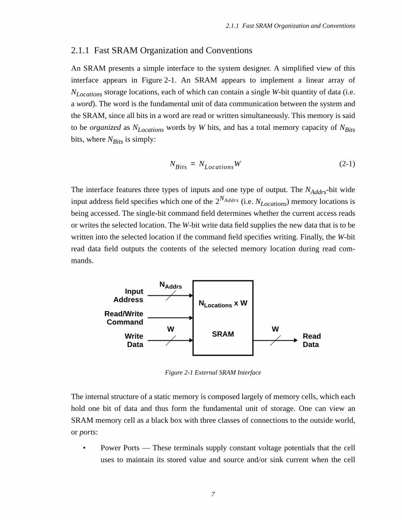
2.1.1 Fast SRAM Organization and Conventions
An SRAM presents a simple interface to the system designer. A simplified view of this
interface appears in Figure 2-1. An SRAM appears to implement a linear array of
NLocations storage locations, each of which can contain a singleW-bit quantity of data (i.e.
aword). The word is the fundamental unit of data communication between the system and
the SRAM, since all bits in a word are read or written simultaneously. This memory is said
to beorganized asNLocations words byW bits, and has a total memory capacity ofNBits
bits, whereNBits is simply:
(2-1)
The interface features three types of inputs and one type of output. TheNAddrs-bit wide
input address field specifies which one of the (i.e.NLocations) memory locations is
being accessed. The single-bit command field determines whether the current access reads
or writes the selected location. TheW-bit write data field supplies the new data that is to be
written into the selected location if the command field specifies writing. Finally, theW-bit
read data field outputs the contents of the selected memory location during read com-
mands.
The internal structure of a static memory is composed largely of memory cells, which each
hold one bit of data and thus form the fundamental unit of storage. One can view an
SRAM memory cell as a black box with three classes of connections to the outside world,
or ports:
• Power Ports — These terminals supply constant voltage potentials that the cell
uses to maintain its stored value and source and/or sink current when the cell
NBits NLocationsW=
2NAddrs
NAddrs
W W
NLocations x W
SRAM
InputAddress
Read/WriteCommand
WriteData
ReadData
Figure 2-1 External SRAM Interface

2.1.1 Fast SRAM Organization and Conventions
8
communicates through its other ports. These ports usually are omitted from block
diagrams and schematics because they convey no signalling information and con-
nect every cell together. There are typically two such ports per cell.
• Selection Ports — These ports select a given cell to be read and/or written, usually
via a change in voltage potential. This thesis consistently draws the physical wires
that connect the selection ports of memory cells as horizontal lines and terms them
word lines; a word line is a wire that selects (at least) one word’s width of bits.
There is usually one such port per cell.
• Communication Ports — Values read from or written to the memory cell pass
through the communication ports. This thesis consistently terms the wires that
connect these memory cell ports asbit lines because they allow the transmission
of the stored single-bit values into and out of the cell; bit lines appear as vertical
lines in SRAM diagrams. There is typically one communication port per cell, but
it often involves a pair of differential bit lines that communicate complementary
data values.
The memory cells are designed to tile into two-dimensional arrays, with the word lines
connected to each cell in a row, and the bit lines connected to each cell in a column. While
the external organization would suggest a memory arrayNLocations words tall by one word
wide, physical constraints that arise from the fact thatNLocations is typically many thou-
sand times larger thanW require an internal organization with an aspect ratio much closer
to unity. As depicted in Figure 2-2, the tall thin logical array may be folded into a nearly
square physical array such that a single word line selects multiple words simultaneously.
The blocks outside the memory array convert the address, command, and data values pre-
sented by the controlling system into the appropriate word line and bit line signalling
required to access the array. In particular, therow decoder selects the word line that con-
tains the desired word, while thecolumn decoder selects the requested word from among
those selected by the word line. By constraining the number of rows per array (NRows) and
the number of words per column (NCols) to each be powers of two, the addresses for the
row and column decoders are trivially generated by simply routing bits of the
input address to the row decoder, and the remaining bits to the column
decoder. Meanwhile, the command and write data inputs direct thecolumn read/write cir-
cuitry to either sense the read data from, or write the input data to, the bit lines of the
selected word. Both the decode and column read/write circuitry deserve additional men-
tion, since they greatly affect the overall SRAM performance.
log2NRowslog2NCols

2.1.2 Decoders
9
2.1.2 Decoders
Decoders perform a logically simple function that turns out to be fairly complicated to
implement in a high-performance way. The goal is quite straightforward: given anN-bit
input address, select whichever of the 2N output lines is identified by the address. Given
true and complemented versions of each address bit, decoding reduces to simply aN-input
AND gate for each output line; the correspondence between output lines and addresses is
programmed by choosing which version of each input bit (i.e. true or complemented) to
connect to the inputs of eachAND gate. High-speed decoder design is more complex
because as the memory capacity increases, the number of address bits rise so the number
of inputs perAND gate (i.e. the gatefan-in) increases. Since increasedfan-in gates have
higher delay, most large SRAM decoders use multiple stages ofAND logic that each have
lower delay due to reducedfan-in. In addition, increasing capacity also increases the num-
ber of memory cells affected by each decoder output, which is to say that the gatefan-out
goes up. Increasingfan-out further complicates the design, since the delay of logic gates
MemCell
BitLine
Row
Decoder
Column Read/Write
Column
(NCols W) Bit Line Pairs
NRowsWordLines
NAddrs
W
W
InputAddress
Read/WriteCommand
WriteData
ReadData
Decoder
WordLine
PairNRowAd
NColAd
MemCell
MemCell
MemCell
Figure 2-2 Internal SRAM Organization

2.1.2 Decoders
10
increases withfan-out. Many SRAMs add additional gain stages to their decoders to
quickly drive large loads.
While the decoding structures described later in this chapter, and in Chapter 3, have many
differences, they all follow the basic structure of Figure 2-3. Theinput buffers increase the
signal strength of theN input addresses to drive the capacitance of the decoder gates,
while generating (at least) true and complemented versions of each input on theaddress
line outputs. For multi-stage decoders, the input buffers typically include the first decod-
ing stage and thus producepre-decoded address lines, where each line represents a logical
conjunction of two or more inputs.1 The address lines select the desired decoderAND
gate, which in turns selects adriver that increases the signal strength to handle the large
fan-out of the array (for row drivers), or generates control signals for the column
read/write circuitry.
1The number of bits pre-decoded by each input buffer is often two, because the four wiresneeded to communicate the four possible states of two bits is no more than what isrequired to send both true and complement versions of two addresses; beyond three bits ofpre-decoding the number of required wires grows rapidly, increasing both the requiredrouting area and the total decoder wiring capacitance.
NInputs
2N
Outputs
2NAddress Lines
InputBuffers
ANDGates
OutputDrivers
Figure 2-3 Basic Decoder Structure

2.1.3 Column Read/Write Circuits
11
2.1.3 Column Read/Write Circuits
The column read/write circuits also have a simple logical description that is substantially
more difficult to implement for large, high-speed SRAMs. On a read access, the column
decoder directs the read/write circuits to steer the bit line data from the selected word to
the output buffer, which drives the read data to the system. The logic that steers one of
many inputs to the output is known as amultiplexer. As the memory capacity increases,
both the number of inputs to each multiplexer and the number of cells on each bit line rise.
The increased capacitance is especially difficult on the bit lines, since the read current
from a memory cell is typically not high enough to rapidly charge the parasitic capacitance
from hundreds or thousands of other memory cells on the same bit line. As a result, fast
SRAMs often use low-swing signalling for reading their bit lines; the basic idea is to begin
each read with the differential bit lines at the same potential, and then to amplify the dif-
ference between the bit lines that develops once the word line selects the memory cell.
Unfortunately, thesense amplifier typically requires too much power and physical space to
implement with each bit line pair. Thus, the sense amplifiers typically operate on the out-
puts of the multiplexers. However, this arrangement adds the large capacitance of the mul-
tiplexer onto the bit line capacitance, which slows the access. Instead of paying this access
penalty, many memories break the multiplexer into stages with reduced capacitance and
insert a sense amplifier between the first and second stages; for very large memories the
intermediate multiplexer capacitance is often high enough that adopting low-swing signal-
ling between multiplexers (with additional sense amplifiers) provides higher performance.
On a write access, the input write data must be steered to the bit lines of the selected word;
because this logic steers one value to one of many places, it is known asdemultiplexing.
While most CMOS SRAMs once used the same bidirectional pass transistors to accom-
plish both multiplexing and demultiplexing, many fast SRAMs now have parallel paths so
that the read path may use smaller swings than the write path and so the memory may
begin a write access as soon as a previous read has cleared the bit lines. The write circuits
typically get little benefit from low-swing signalling, since the devices that drive the
demultiplexer and the bit lines can be much larger than the devices attached to the bit
lines, so traditional buffering works quite well.
2.1.4 Banks
While both decoders and read/write circuits may be modified to maintain certain perfor-
mance parameters as memory capacity increases, intrinsic problems with the memory

2.1.4 Banks
12
array itself eventually begin to reduce the performance. This performance degradation
arises from several factors. All the memory cells on the selected word line attempt to
charge their bit line capacitance, independent of whether the bit lines are part of the
selected word. Thus, very long word lines waste lots of power in charging unselected bit
lines. A second factor is the intrinsic delay of the wires that form the word and bit lines; as
the arrays grow, so does both the resistance of these wires and the capacitance that loads
them. As a result, the distributed wireRC delay grows as the square of the array dimen-
sions, which slows the access time. Finally, the number of cells on a bit line begins to slow
the access, since there are practical limits to how small a bit line swing may be reliably
sensed.
Rather than tolerate the performance limitations of large arrays, SRAM designers avoid
these problems by using several smaller arrays (often termedbanks). For example,
Figure 2-4 depicts a large memory array which is then broken into four smaller arrays. The
smaller arrays have higher performance because they feature fewer cells per word line and
bit line. However, there is a penalty to this approach: the required amount of decoding
increases. In the figure, the number of decoder gates doubles, since the number of both
word and bit lines doubled when the arrays were split apart. Furthermore, thefan-in of the
decoders increases. Considering the row decoders in the example, the individual decoder
blocks control half as many word lines as those in the large array, which requires one less
bit of decoding. However, these decoders also must select between the four banks, since
only one word line should be selected at once to reduce the power in unselected cells; this
extra decoding requires two additional bits of decoding, so the decoderAND gates in the
four-bank case each have one more input than those of the single array.
The increased decoding that results from banked SRAM designs limits the memory per-
formance in several ways. The increased decoderfan-in slows the access. The increased
die area devoted to decoding reduces the memory capacity. Finally, for technologies such
as ECL where the basic decoder dissipates static power, the decoding power increases in
proportion to the number of decoders. As a result, designing large and fast SRAMs
requires complex analysis to determine the appropriate array sizing and organization to
maximize performance. The next sections look at these tradeoffs for CMOS, bipolar, and
BiCMOS SRAMs.

2.2 CMOS Static Memories
13
2.2 CMOS Static Memories
SRAMs implemented in CMOS technologies dominate the marketplace, because CMOS
memories offer low power and high capacity solutions. Traditionally, CMOS SRAMs
were much slower than the bipolar alternatives, but rapid improvement in CMOS device
performance due to technology scaling and innovative circuit design technique shave
greatly narrowed the gap. This section describes the design of fast CMOS SRAMs, with
an emphasis on understanding the advantages of CMOS technology that will be exploited
by the circuits of this thesis.
Complementary MOS (CMOS) circuit technology takes advantage of the insulating gate
terminal and near-zero “off” current of the Metal-Oxide-Semiconductor Field-Effect Tran-
sistor (MOSFET) to implement logic gates that dissipate nearly-zero static power. By uti-
lizing n-channel and p-channel MOSFETs (i.e. NMOS and PMOS transistors), which have
opposite threshold voltages, classic CMOS circuits implement switch networks that guar-
antee that no current paths exist between the power supplies once the inputs transition; the
action of the switches connects the output to one of the supplies while isolating the output
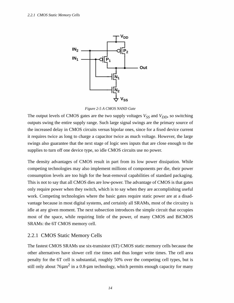
from the other supply. For example, in the CMOSNAND gate of Figure 2-5, the output is
high (VDD) if either input is high, since one or both of PMOS transistorsP1 andP2 are
conducting and the output is isolated from the low supply (VSS) by at least one of the
series-connected NMOS devices. The output is low only if both inputs are low, where the
only conducting path is toVSS via N1 andN2.
Figure 2-4 Banked SRAM Organization
Cell
Array
Column Decoder
VS.
Row
Decoder
Dec
Cell
Array
Column Decoder
Dec
Cell
Array
Row
Cell
Array
Column Decoder
Row
Cell
Array
2.2.1 CMOS Static Memory Cells
14
The output levels of CMOS gates are the two supply voltagesVSS andVDD, so switching
outputs swing the entire supply range. Such large signal swings are the primary source of
the increased delay in CMOS circuits versus bipolar ones, since for a fixed device current
it requires twice as long to charge a capacitor twice as much voltage. However, the large
swings also guarantee that the next stage of logic sees inputs that are close enough to the
supplies to turn off one device type, so idle CMOS circuits use no power.
The density advantages of CMOS result in part from its low power dissipation. While
competing technologies may also implement millions of components per die, their power
consumption levels are too high for the heat-removal capabilities of standard packaging.
This is not to say that all CMOS dies are low-power. The advantage of CMOS is that gates
only require power when they switch, which is to say when they are accomplishing useful
work. Competing technologies where the basic gates require static power are at a disad-
vantage because in most digital systems, and certainly all SRAMs, most of the circuitry is
idle at any given moment. The next subsection introduces the simple circuit that occupies
most of the space, while requiring little of the power, of many CMOS and BiCMOS
SRAMs: the 6T CMOS memory cell.
2.2.1 CMOS Static Memory Cells
The fastest CMOS SRAMs use six-transistor (6T) CMOS static memory cells because the
other alternatives have slower cell rise times and thus longer write times. The cell area
penalty for the 6T cell is substantial, roughly 50% over the competing cell types, but is
still only about 76µm2 in a 0.8-µm technology, which permits enough capacity for many
N1
P1
VSS
N2
P2
VDD
IN2
IN1
Out
Figure 2-5 A CMOS NAND Gate

2.2.1 CMOS Static Memory Cells
15
applications. Furthermore, because the 6T cell requires only bulk PMOS and NMOS
devices, 6T cell-based SRAMs are often implemented on the same integrated circuit as
other parts of the system that uses the SRAM, which improves system integration.
The 6T cell itself is quite simple. Two CMOS inverters with each inverter’s output con-
nected to the other inverter’s input (cross-coupled) create a very stable, nearly zero power
latch that is the basis for the memory cell shown in Figure 2-6. The latching operation is
very simple: if nodeD is higher than the switching threshold of theN2-P2 inverter then
NMOS deviceN2 pulls down nodeD, in turn causingP1 to pull nodeD higher. This pos-
itive feedback action forcesD = VDD andD = VSS, (neglecting any effects ofN3 andN4).
We say that the memory cell stores one when nodeD is high andD low. Similarly, if the
cell stores zero thenD is low and the positive feedback forcesD high. The leakage current
in such a latch is very small. In common bipolar memories the storage current per memory
cell is less than 10-15Amps (1femtoAmp), so the idle current of a megabit memory array
is less than 1nA. Thus CMOS memory arrays require very little standby power.
The latched value is both altered and read through the NMOS access devicesN3 andN4.
Because PMOS transistors have higher on resistances than NMOS devices of the same
size, it is simplest to flip the cell state by overpowering a PMOS device by pulling down
its drain with the NMOS access device on the same side. This memory cell is written by
raising the word line, often toVDD, and pulling the bit line down toVSS on the cell side
that needs to be low. For instance, if a cell storing one is to be flipped then nodeD needs to
drop so the bit line driver pullsBitLine to VSS which causes access transistorN3 to fight
N3
VSS
P2 P1
N2 N1
N4
VDD
DD
Word Line
Bit LineBit Line
Figure 2-6 A 6T CMOS Memory Cell

2.2.2 Complete CMOS SRAMs
16
P2. N3 easily dropsD low enough forP2 to begin turning on and then the latching action
will rapidly finish flipping the internal cell nodes.
External circuitry can read the cell by raising the word line without driving either bit line.
The cell access transistors then discharge one bit line towardsVSS and charges the other
towardsVDD – VTh. The high capacitance of the bit line presents a problem in reading the
cell: when the word line first rises, the bit lines do not immediately change so they appear
like voltage sources. If a read access begins with a bit line voltage that is too low, the
access device will fight its PMOS device and may inadvertently flip the cell on a read
access. Since NMOS transistors pull down more strongly than up, it is difficult to over-
power an NMOS inverter device with the NMOS access transistor. Thus, higher bit line
potentials are much less likely to unintentionally write a cell. The situation is often
improved by makingN1-N2 have higher drive strength (i.e. largerW/L) than N3-N4,
which makes it impossible to disturb the cell value with a high bit line potential. Thus, the
column read/write circuits must ensure that the bit lines are at safe (i.e. relatively high)
levels before the word line rises to begin a read access.
A 6T CMOS cell can provide very fast read access, since the cell begins pulling on the bit
line as soon as the word line rises pastVTh. The issues in making CMOS SRAMs go fast
have much more to do with quickly raising the word line, and rapidly sensing the bit lines.
2.2.2 Complete CMOS SRAMs
The read access path of current megabit-class CMOS SRAMs have many (twenty or more)
address pins and therefore require lots of decoding. As a result, CMOS decoders often uti-
lize three or more stages of decoding to avoid the delay associated with ten-input series
MOS transistor gating. For the sake of clarity Figure 2-7 presents a simplified view of a
CMOS read path that retains the major circuit types present in fast CMOS SRAMs.
The input buffer generates true and complemented versions of each address bit, which are
used to drive pre-decoded address lines. This pre-decoding is typically performed in two
or three bit groups by a CMOSNAND gate followed by a inverter, with the inverter pro-
viding load-driving capability (using large device width) as well as the required logical
inversion to implement the pre-decodeAND function. The pre-decoded address lines are
typically heavily loaded because they run the entire height of the row decoder and there-
fore have substantial wire capacitance along with the loading from the gate capacitance of
the row decoders.

2.2.2 Complete CMOS SRAMs
17
Multi-input NAND gates also form the row decoder, often using small devices to minimize
the loading on the address lines. The row decoder output is complemented and increased
in drive capability by one or more inverters to control the heavily-loaded word line and
thus access the memory cell.
The column decoder is implemented like the row decoder, and controls the column multi-
plexer to select which pair of bit lines are connected to the shareddata lines via PMOS
transistorsPD1 andPD2. The bit line load transistorsPL1 andPL2 are weak PMOS
devices that prevent the bit lines from dropping to unsafe levels (where newly-selected
cells might be accidentally written) during reads; they are weak enough to be easily over-
powered during intentional cell writes. A memory cell on a selected word line and selected
bit lines pulls a currentIRead from the bit line on the low side of the cell. This current dis-
charges the bit line capacitance, as well as the connected data line capacitance, until the bit
line voltage drops enough that the bit line load will sourceIRead. Meanwhile, the bit line
load on the complementary bit line charges its data line towardsVDD – VTh. The voltage
difference between the data lines is detected by the sense amplifier. The output of the
sense amplifier goes to the output buffer, which increases the drive strength of the signal
and completes the access.
PL1
Memory Cell
PD1PD2
PL2
Pre-Decode Decode
Input Address
From Column Decode
Data Lines
Figure 2-7 Simplified CMOS SRAM Read Access Path

2.2.3 Reducing CMOS SRAM Delay
18
2.2.3 Reducing CMOS SRAM Delay
The critical path through a large SRAM would normally pass through the row decoder,
word line driver and then the sense amp; the column decoder has a little more time to
accomplish its task, so it normally does not delay the read access. A fast SRAM therefore
requires rapid word line decoding and driving, as well as quick bit line sensing.
Minimizing the word line delays requires effectively integrating the logical decode func-
tion with the largefan-out requirements. Since each row address bit can select every word
line, each address bit has a totalfan-out of the number of word lines times the loading on
each word lineCWL divided by the input buffer’s input loadingCIB, i.e.
(2-2)
The actualfan-out is higher because the decode gates utilize series gating, which provides
lower output drive per unit of input capacitance than do inverters. CMOS inverter chains
provide minimum load driving delays when the number of stages is set so that thefan-out
per stage is approximatelye [9]. This explains why large row decoders for fast SRAMs
often use ten or more inverting gates to turn a row address into a word line transition. With
so many gates to work with, such decoders typically further reduce delay by distributing
the decode function among multiple gates beyond one level of pre-decoding.
A common method to improve the speed of CMOS logic chains is to use synchronous (i.e.
clocked) design styles, which begin each access in a fixedreset state and then condition-
ally transition to the active state. For fast SRAMs, only one decoder output should ever be
selected so the number of transitions in a clocked decoder is fairly small and thus power
dissipation does not change much. More importantly, the transistors in the clocked gates
may be sized to minimize the delay of the active-going transition, since the reset transition
is generated via the clock and is thus independent. For instance, if the NMOS devices in
the row decoder’sNAND gates are increased in width versus the PMOS’ width, theNAND
output will begin falling at a lower input value (and hence earlier in the input’s rising tran-
sition) and will supply more current and thus discharge its load more rapidly. If the
NMOS/PMOS width ratio is increased such that the total input load is constant, then the
PMOS width must decrease and thus the rising delay will increase. If a PMOS device is
added in parallel with the other PMOS transistors with its gate activated by the reset clock,
the rising delay is improved without sacrificing the fast falling delay.
fan-out 2NRows
CWL
CIB=

2.2.3 Reducing CMOS SRAM Delay
19
CMOS logic gates with extra reset transistors form the basis for designs usingpost-charge
logic [10 11] or the similarself-resetting circuits [12 13]. In order to let the selection
devices be as wide as possible for a given input capacitance, these techniques make the
deselection devices too weak to meet the required deselection delay. Instead, additional
reset devices are added in parallel to the weak transistor and are activated by a delayed
version of the selection signal output from the same gate; in other words, after the gate
fires (i.e. switches to a selected state), its own output is fed back to reset the gate after a
fixed delay (usually a few inverter delays), orpost-charged.
TheRC delay of the word lines is very significant for large CMOS SRAMs, which often
have several thousand cells per row. Thedivided word line technique [14] reduces this
delay by allocating two word lines for each row. The higher-resistanceglobal word line
runs the entire length of a row, and connects only to a set of buffers distributed along the
row. The buffers drive much shorterlocal word lines that connect to the access transistors
of the memory cells. This technique minimizes delay by reducing the capacitance of the
long wires. The local word line buffers typically provide an additional level of decoding
that ensures that only one local word line is high, and thus that only a subset of the cells on
a row are selected.
Decoding the address inputs and driving the word lines takes about half the access time.
The remaining delay is spent sensing the stored data and driving the output pins. The pri-
mary techniques used to reduce CMOS sensing delays involve extensive use of low volt-
age swing circuits to minimize the time required to charge the large capacitances present
on the shared bit and data lines. The load problem is greatest on the bit lines, where one
NMOS access device must move a wire connected to the drain terminal of every other
access device on that bit line, as mentioned in Section 2.1.1. In order to minimize the
delay, the bit line load devices become much strongerclamp devices, only active during
reads, that guarantee that the bit lines begin an access at very nearly the same potential.
The clamp transistors also limit the bit line read swings to minimize the bit line recovery
time while ensuring that the sense amplifier has enough differential swing to resolve. Fast
SRAMs minimize the delay by minimizing the required swing; as long as the bit lines start
off at the same potential, delay will reduce as the sense amplifier sensitivity increases.
Clocks are often used to activate the clamp devices to rapidly restore the bit line voltages
following write cycles.
Because there are often thousands of columns in a SRAM, there is also a delay problem
due to the high level of multiplexing required on the shared data lines. In order to reduce

2.3 Bipolar Static Memories
20
this delay, many SRAMs utilize several levels of data lines (and hence multiplexing) with
sense amplifiers connecting each level to the next, which allows the SRAM to improve the
delay both by reducing the total capacitance in the access path and by reducing the voltage
swings along each stage in the path.
The resulting CMOS SRAMs deliver access times that are much closer to those of bipolar
SRAMs than is possible using traditional full-swing CMOS circuits [15]. The penalty of
low-swing signalling is increased power dissipation, since the increased-sensitivity sense
amplifiers use substantially more power than the full-swing circuits that they replace.
However, as the next section shows, fast CMOS SRAMs use substantially less power than
their bipolar counterparts, primarily due to the lack of static current in the memory cells.
2.3 Bipolar Static Memories
This section describes the design of bipolar SRAMs, which have delivered the fastest
access and cycle times of any silicon-based technology [16 17 18 19 20]. Bipolar
decoding and sense techniques used in these memories are the basis for some of the new
techniques presented in this thesis.
The low-swing ECL bipolar logic circuits that implement the decoders are particularly
interesting because they offer much faster switching speeds than CMOS circuits, although
they use static current sources that substantially increase their power dissipation. In order
to better understand the speed advantage of bipolar circuits, consider the ECLNOR gate of
Figure 2-8. Bipolar junction transistors (BJTs) transistorsQ1, Q2, andQ3 form a simple
current switch that performs the desired logical function: the shared current (IGate) is
switched into the load resistor (RGate) if either input is higher than the reference (VRef),
andIGate thus flows throughQ3 only if both inputs are belowVRef. Theemitter follower
formed byQ4 andIEF isolatesRGate from the output capacitance (CLoad), and so the gate
delay is dominated by theRC term arising fromRGate times the capacitance at the shared
collector node (A). For a fixedIGate (i.e. fixed gate power), theRC delay is proportional to
the gate swing (VSwing), since
(2-3)
Thus, ECL circuits switch faster asVSwing is reduced. Practical considerations limit the
minimum swing to be about 700mV in most ECL systems, which is much smaller than the
VSwing IGateRGate=

2.3 Bipolar Static Memories
21
3-V to 5-V swings common in CMOS systems. This speed advantage comes at the
expense of power dissipation, sinceIGate andIEF flow continuously, rather than only when
the gate is switching.
The emitter follower supplies a lesser portion of the bipolar speed advantage. The high
forward current gain (β) of the BJT makes the emitter follower an excellent buffer for
driving largefan-out. While output ringing considerations under high-gain conditions typ-
ically limit the IEF/IGate ratio at traditional ECL logic swings to around five, this signal
strength improvement is achieved without using a level-restoring gate, so the delay is
reduced. The emitter follower delay is typically one third that of a level-restoring gate, so
emitter followers greatly improve the delay of highfan-out structures like decoders.
Besides its use for rapidly driving large loads from relatively low power gates, the emitter
follower also provides a key ECL logical function: the outputs of several ECL gates (with
emitter follower outputs) may be connected together, resulting in a shared output that is
high if any of the gate outputs are high. This interconnection of emitter follower circuits
thus performs the logicalOR function and is called awired-or because the function is per-
formed simply bywiring the gate outputs together. The wired-or is better than anOR func-
tion built with current-switching stages because it is faster (runs at emitter follower rather
than current switch speeds) and requires fewer devices.
Because the output of an emitter follower is oneVBE below its input, emitter followers
implement a level shift that enables the use of stacked ECL current switches that do not
saturate. This thesis labels signals that have been throughN VBE drops asLN. Thus, node
A in the Figure 2-8 isL0, while the gate output isL1. A two-level stack of current switches
Q2Q3
RGate
Q1
IGate
VRef
Q4
IEF
In1
In2
Out
CLoad
A
Figure 2-8 An ECL NOR Gate

2.3.1 Bipolar Static Memory Cells
22
with L1 inputs on the top level would thus requireL2 inputs on the bottom level to avoid
saturating the BJTs in the bottom stack.
With this background in place, the speed advantages of the bipolar memory cell, with its
low-swing word line and high read current will be clear. Unfortunately, the static power
dissipation of the cell makes it unsuitable for most high-capacity SRAMs.
2.3.1 Bipolar Static Memory Cells
The fastest bipolar SRAMs use theSchottky Barrier Diode (SBD) loadmemory cell [16],
which is depicted in Figure 2-9. The SBD load cell stores its data in a latch formed by the
multi-emitter transistorsQ1 andQ2, and the load resistorsRH1 andRH2. Assuming that
both bit line-connected cell emitters conduct no current and that nodeD is higher thanD,
most of the currentIStdby flows throughQ2, causing aIStdbyRH2 drop from the word line,
WordLine1, to D. SinceQ1 conducts almost no current,RH1 supplies only the base cur-
rent for Q2 and henceD is at about the same potential asWordLine1. Thus the cell
latches into a state with a voltage difference between internal cell nodes of about
IStdbyRH, assuming this value is less than the turn-on voltage of the SBD.
Q2 Q1
RL1
QBL2
IStby
VCC
SBD1RH1
RL2
SBD2RH2
IBL2
QBL1
IBL1
DD
WordLine1
BitLine1BitLine2
FromRead/Write
Circuits
Figure 2-9 Schottky Barrier Diode Load Memory Cell

2.3.1 Bipolar Static Memory Cells
23
In order to read the cell, the word line driver raisesWordLine1 by about 0.8V, which
would tend to raise bothD andD by the same amount in the absence of the bit line cir-
cuits. The external bit line circuits consist of pull-down current sourcesIBL1 andIBL2, and
common emitter BJTsQBL1 andQBL2 that prevent the off-side cell transistor from turn-
ing on during reads. Because the bases ofQBL1 andQBL2 are set at roughly the midpoint
of theWordLine1 swing, the cell transistor whose base voltage is higher (Q2 in this case)
conducts most ofIBL while, on the other bit line,D is lower than the reference and thus
QBL1 steers most of the current. In this wayBitLine2 charges to oneVBE below
WordLine1, whileBitLine1 is clamped byQBL1; the bit line voltage difference is readily
sensed using a differential pair to finish the read access.
The preceding assumes that theIBL running throughQ2 does not greatly affectD andD;
the purpose of the SBDs is to make this true. In order to minimize the power required to
keep the cells latched,IStdby should be set as low as the following restrictions allow;IStdby
is typically around 10µA. A small IStdby implies a large value forRH (tens of kΩ), and if
the cell read currentIBL had to flow throughRH this would limitIBL to be a small multiple
of IStdby in order to prevent bipolar saturation in the cell. Because a large value ofIBL
(roughly 1mA) is desired to rapidly move the heavily-loaded bit lines, SBDs are added to
the cell in parallel withRH to supply the cell read current without much added voltage
drop. In other words, the SBDs allow a much larger ratio ofIBL to IStdby than would other-
wise be possible. SBDs are chosen over junction diodes because they have a lower turn-on
voltage than the BJT’sVBE, which prevents the transistor supplying the read current from
becoming saturated, and because SBDs require less cell area than junction diodes.
For read to standby current ratios approachingβ the base current ofQ2 during a cell read
is large enough to cause significant drops across its base resistorRH1. This tends to
decrease the voltage difference betweenD andD. RL1 andRL2 add a resistive component
to the SBD load curves that somewhat limits the reduction in voltage margin, but poor
matching of component values limit the usefulness of this approach. This decrease in the
high cell voltage during reads therefore limits the practically achievable active to standby
current ratios, and leads to significant standby power in large bipolar memory arrays.
Peripheral circuits write the cell by raising the word line to its selected value, and pulling
current from the cell transistor whose collector node should be low. If that side of the cell
already happens to be low then the cell state does not change. However, flipping the cell
requires pulling current from the transistor with the low cell potential on its base, so the
base of that bit line’s clamp device must be lowered so the bit line is free to drop enough to

2.3.2 Complete Bipolar SRAMs
24
turn on the cell transistor. Meanwhile, the other clamp device should raise the other bit
line so no read current flows through the other cell transistor. For example, to write a cell
that stores one to zero,QBL2 raisesBitLine2 soQ2 does not supplyIBL, whileQBL1 lets
BitLine1 drop untilQ1 turns on. OnceQ1 turns on,IBL dischargesD until it drops below
D, at which pointIStdby switches toQ1 and thusD rises to complete the write.
The read current supported by the SBD load cell is much larger than that of a 6T CMOS
cell, and hence provides faster bit line sensing, especially with the excellent voltage sensi-
tivity of bipolar differential amplifiers. Furthermore, rapid cell reads and writes require
only low-swing signals, which makes the cell a good match for extremely-fast ECL bipo-
lar decoders.
2.3.2 Complete Bipolar SRAMs
The peripheral circuits of a bipolar SRAM require careful design to deliver the fast access
permitted by the memory cell. After detailing two options for the decoding function, this
section discusses an example implementation of a bipolar SRAM access path.
Traditional bipolar decoders fall into two categories based upon the basic decoding gate.
Because the logicalAND function implemented by a decoder would require many-level
series stacking to construct from standard ECL structures, bipolar decoders are typically
built either from ECLNOR gates with complemented inputs orAND gates built using
diode logic.
The diodeAND gate that implements thediode decoder [21] is shown in Figure 2-10; it
implements theAND function because the output is low if any of the inputs are low. Like
ECL gates, the diode decoder uses a resistor to passively pull the output to the high state
and therefore requires static current to keep its output low. Unlike an ECL gate, however,
this static current is supplied through the input diodes so the output of a diode decoder
begins to change as its inputs change, rather than once the inputs cross a threshold. The
diode decoder therefore offers the potential of lower delay than the (ECL gate-based)NOR
decoder, assuming equivalent input transition times. However, the decoder output swing is
determined by the input swing since there is no level-restoring gate.
The figure also shows the ECLNOR gate that is the basis of aNOR decoder. While it nor-
mally requires extra inverters on the inputs of aNOR gate to implement theAND function,
the address lines of a decoder usually have both true and complemented versions of each
address, so the input inversion reduces to simple rewiring. Since theNOR inputs are active
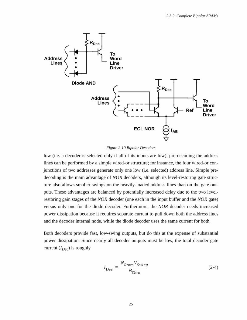
2.3.2 Complete Bipolar SRAMs
25
low (i.e. a decoder is selected only if all of its inputs are low), pre-decoding the address
lines can be performed by a simple wired-or structure; for instance, the four wired-or con-
junctions of two addresses generate only one low (i.e. selected) address line. Simple pre-
decoding is the main advantage ofNOR decoders, although its level-restoring gate struc-
ture also allows smaller swings on the heavily-loaded address lines than on the gate out-
puts. These advantages are balanced by potentially increased delay due to the two level-
restoring gain stages of theNOR decoder (one each in the input buffer and theNOR gate)
versus only one for the diode decoder. Furthermore, theNOR decoder needs increased
power dissipation because it requires separate current to pull down both the address lines
and the decoder internal node, while the diode decoder uses the same current for both.
Both decoders provide fast, low-swing outputs, but do this at the expense of substantial
power dissipation. Since nearly all decoder outputs must be low, the total decoder gate
current (IDec) is roughly
(2-4)
RDec
Diode ANDRDec
IAB
Ref
ToWordLineDriver
AddressLines
AddressLines
ToWordLineDriver
ECL NOR
Figure 2-10 Bipolar Decoders
IDec
NRowsVSwing
RDec=

2.3.2 Complete Bipolar SRAMs
26
for each decoder type, whereVSwing is the decoder output swing andRDec is the load
resistance.RDec must be fairly low for fast access, so the decoding power is often the sec-
ond largest component of bipolar SRAM power dissipation after the memory cells. Chap-
ter 3 introduces techniques that greatly improve the power dissipation of low-swing
decoders.
Figure 2-11 depicts the read access path of a typical high-speed bipolar SRAM, consisting
of input buffers with pre-decoded outputs,NOR decoders, Darlington word line drivers,
SBD load memory cells, bit line decoders and pre-amplifiers, cascode sense amplifiers,
and output buffers. A brief description of each circuit follows.
Each input buffer consists of an ECL inverter with complementary outputs connected to
pre-decoded wired-or address lines. This wired-or structure produces very fast pre-
decoded outputs, since the delay is increased only by the extra parasitic capacitance of the
second emitter of each emitter follower on the inverter. Many technologies allow sharing
of the collector and base regions of the followers to minimize this capacitance.
The pre-decoded address lines drive the ECLNOR decoder gates. Pre-decoding makes
these decoders faster because of reduced base-collector and collector-substrate capaci-
tance on the decoder output node. A decoder output controls a pair of cascaded emitter fol-
lowers that drives a word line across the memory cell array. Such a connection of emitter
followers is often called aDarlington pair and is capable of rapidly driving large capaci-
tances because the effective current gains of each stage are multiplied. The pull-down cur-
rent source in the middle of the Darlington helps speed the falling transition, which is
otherwise discharged only by the base current of the second BJT.
The stored data values for memory cells on the selected word line are sampled only if the
cell is also connected to a selected bit line pair. The column decoder selects a pair of bit
lines by steeringIBLCS into both bit lines andIPre into their differential pair. Meanwhile,
both bit line clamp devices are set to a base potential midway in the word line swing. As
described in Section 2.3.1, a voltage difference develops on the bit lines due to the cell
state; this difference causes thepre-amplifier, (i.e. the differential pair), to pull different
currents from the data lines, which are shared with the other unselected columns. The
sensed currents may be turned back into voltages with a resistor, but the large loading on
the data lines (due to potentially very many unselected pre-amplifiers) would give a large
delay if the resistors were attached directly to the data lines.

2.3
.2 C
om
ple
te B
ipo
lar S
RA
Ms
27
MemCell
IBLCSIPreIBLCS
CascodeOutput
Data
InputAddress
Wire-OrPre-DecodedAddressLines
DataLines
FromColumnDecode
Ref
NORDecode
Figure 2-11 Bipolar SRAM Read Access Path

2.4 BiCMOS Static Memories
28
BJTs with reference voltages on their bases and inputs at their emitters, in what is known
as acascode configuration [22], provide large output current differences with very low
input swings (60mV per decade of current). Since the data line delay is roughly
CDLVSwing/IPre, the cascode sense amplifier greatly reduces the data line voltage swings
and thereby minimizes the data line delay, while providing a lower-capacitance output
node that has greatly-reducedRC delay. The differential output of the sense amplifier then
goes through emitter followers to a final ECL output buffer, which restores the read data to
normal ECL voltage levels and, when the data must be driven off-chip, increases the drive
strength of the signal to rapidly drive a 50-Ω transmission line.
Bipolar SRAMs deliver very fast access due to their low-swing signalling and the excel-
lent voltage sensitivity and current drive capabilities of bipolar transistors. However, the
static power dissipated by the memory cell and the peripheral circuits prevents the use of
this technology for most large memories. BiCMOS SRAMs, which are the subject of the
next section, offer the opportunity to combine the best of CMOS and bipolar SRAMs to
come up with superior solutions.
2.4 BiCMOS Static Memories
By incorporating NMOS, PMOS and NPN BJT devices on the same integrated circuit,
BiCMOS process technology offers the promise of hybrid SRAM solutions that combine
the low power and high capacity characteristics of CMOS with the fast access and cycle
times of bipolar memories. While existing BiCMOS SRAMs achieve
speed/power/capacity combinations that neither CMOS nor bipolar designs can match,
BiCMOS designs do not deliver bipolar speeds at CMOS power levels. Existing BiCMOS
memories bridge the gap between CMOS and bipolar to deliver intermediate speed at
intermediate power [3 23 24 25 26 27 28 29 30 31 32 33 34 35 36]. After
describing two basic BiCMOS design styles, as well as the interfacing problem, the sec-
tion details the brief history of fast BiCMOS static memories.
2.4.1 BiCMOS Design Styles
The two main BiCMOS design styles differ based on the circuit families they imitate. The
first style uses large signal swings and CMOS-derived logic gates, often with bipolar out-
put stages. The canonical example of a large-swing BiCMOS circuit is theBiCMOS buffer
[37], which exists in many flavors. The main advantages of this style over CMOS struc-
tures are improved gate delay versusfan-out characteristics, due to the BJTs, coupled with

2.4.2 Complete BiCMOS SRAMs
29
zero static power dissipation due to the CMOS logic. Furthermore, large-swing BiCMOS
is similar enough to CMOS that many design programs can be simply modified to handle
the new structures. Unfortunately, the large-swing BiCMOS is so similar to CMOS that it
does not provide greatly-enhanced speed.
The competing design style starts with small-swing ECL circuits, which have superior
speed characteristics, and adds MOS transistors to improve power dissipation. The MOS
devices, generally speaking, save power by allowing current-switching ECL logic gates to
be powered down when their outputs cannot change. As long as the critical paths through
such circuits pass mostly through bipolar transistors, the resulting delay is comparable to
ECL bipolar circuits. This thesis is intended as an example of the benefits of low-swing
BiCMOS.
Many BiCMOS systems use both design styles, which requireslevel conversion between
the two signalling domains. The delay and power required to amplify a low-swing signal
to full CMOS levels is often outweighed by the benefits provided by the separate domains.
For instance, a BiCMOS SRAM could use ECL circuits to implement very fast decoders
and CMOS memory arrays to save static power; while the resulting design is somewhat
slower than a bipolar memory, it uses much less power.
2.4.2 Complete BiCMOS SRAMs
The original BiCMOS SRAMs were essentially CMOS SRAMs with a few BJTs added in
the periphery to improve the access time. The improvements were largely due to three
replacements:
• ECL Input/Output (I/O) interface instead of TTL
• BiCMOS buffers instead of CMOS inverter for load drivers
• Bipolar small-swing sensing instead of MOS
The ECL I/O interface helps because the required ECL output swings are readily gener-
ated by a simple ECL inverter with an emitter follower output that drives a well-specified,
terminated transmission line. The electrical environment permits much faster signal transi-
tions than does TTL, and the driver circuit has fewer stages than a TTL output driver does,
so the output delay is substantially reduced. For most BiCMOS SRAMs, the penalty for an
ECL interface is at the input, where small input signals must be converted to full CMOS
levels to drive the memory array. However, the delay penalty for this conversion is offset
by the complexity, and hence delay, of the TTL input buffer, which has amplification

2.4.2 Complete BiCMOS SRAMs
30
requirements of its own. The delay reduction provided by the ECL interface is very signif-
icant: a recent design that can support both interfaces (with a simple mask change) has a
6-ns access time through the ECL interface, but requires 8-ns through the TTL interface
[36].
In order to maintain an access path that looked very much like the well-understood CMOS
SRAM, these early designs converted their ECL inputs to CMOS levels at the input buff-
ers. The converted inputs controlled decoder and driver circuits that were essentially just
the normal CMOS logic gates with BiCMOS buffer-style outputs. The BiCMOS buffers,
having superior load-driving ability, allowed these decoders to drive their word lines with
fewer level-restoring buffer stages and thus less delay.
Replacing the CMOS sense path with bipolar sensing circuits was particularly simple,
especially since the CMOS designs were already copying some of the low swing tech-
niques popular in bipolar SRAMs. In fact, except for the MOS bit line switches, which
allow one bipolar differential pair to be shared among multiple bit line pairs, the sense
path of some BiCMOS SRAMs looks just like a bipolar SRAM, with column-selected dif-
ferential pairs connected to shared data lines whose swing is limited by a cascoded sense
amplifier that feeds a bipolar output buffer.
Nearly all BiCMOS SRAMs reported to date utilize the same memory cells found in
CMOS SRAMs and thereby compete with CMOS for memory density while providing
faster access times. In order to minimize the sense delay of 6T CMOS memory cells, the
cell read current should be maximized, which requires large word line swings. Thus, most
BiCMOS SRAMs require a time-consuming level conversion somewhere between their
inputs and the memory arrays. As was just mentioned, the early designs converted their
inputs at the input buffers. Later designs have gradually moved the level conversion closer
to the word line driver, exchanging fast, high-power ECL decoding structures for slower
but lower power CMOS gates with BiCMOS buffer outputs.
Once the level converter has been moved to the word line driver, the access path of a
BiCMOS SRAM looks very similar, both in decoding and sensing, to that of a bipolar
SRAM and so it is not surprising that the access times are similar. Continued process scal-
ing has reduced the maximum permitted terminal voltages of MOS transistors to around
3V from 5V; this change reduces the supply voltages for CMOS circuits and allows ECL
circuits operating at 5-V supplies to provide CMOS-like swings with simpler level

2.5 Summary
31
converters. An example of this appears in the decoding path of the BiCMOS memory
shown in Figure 2-12, which is modelled after [4].
As the figure shows, the access path is virtually identical to the bipolar path of
Figure 2-11, except for the memory cell itself. The 6T CMOS cell array connects to a neg-
ative supplyVSS that is generated by an on-chip voltage regulator [38] to be about 3V
belowVCC and therefore the maximum voltage constraints on the MOSFETs is satisfied.
The bipolar devices, on the other hand, run off a negative supply of 5.2V and can thereby
directly drive the word line from theNOR decoder with CMOS-like 3VBE swings simply
by increasing the resistanceRDec. TheNOR decoder BJTs do not saturate as long as their
bases get no higher than 3VBE below VCC, which is guaranteed by the wired-or pre-
decoder. The resulting word line levels, i.e. unselected at 4VBE (~VSS) and selected at one
VBE belowVCC, provide a large enough swing to achieve good read current with reason-
able cell device sizes and therefore provides substantially improved access times at mod-
erate density penalties. The main reason bipolar memories are faster than a BiCMOS
SRAM such as Figure 2-12 is simply that the BJTs in a bipolar process have higher perfor-
mance than those in a BiCMOS process. However, along with bipolar-class access times
comes bipolar-class power dissipation, since although the CMOS memory cell array dissi-
pates very little power, the bipolar peripheral circuits have high power dissipation, espe-
cially for large memory capacities with multiple banks of decoders [5].
2.5 Summary
Designers have spent an enormous amount of effort to improve the speed of static memo-
ries as the capacity increases. Larger memories need more decoding and have larger inter-
connect loading, so gatefan-in andfan-out are constant issues. The increasing delay and
power consumption of large memory arrays leads to the use of smaller memory banks,
which require more decoders with higherfan-in. Furthermore, the large amount of multi-
plexing in the sense path often leads to multiple low-swing stages for fast access.
SRAMs fabricated in different technologies adapt to these challenges in different ways.
Fast CMOS SRAMs derive substantial power advantage from zero static power memory
cells and large-swing logic. However, the large-swing logic has higher delay than small-
swing logic, so CMOS SRAMs often use complex clocking schemes and low-swing bipo-
lar-derived sense circuits to speed their access. Meanwhile, bipolar SRAMs are typically
much simpler and faster, because basic ECL circuits switch very rapidly and can drive

2.5
Su
mm
ary
32
Figure 2-12 BiCMOS SRAM Read Access Path
RDec
MemCell
IBLCSIPreIBLCS
OutputData
InputAddress
DataLines
FromColumnDecode
VSS
Gen.
VSS
VEE
(-5.2V)
VCC (0V)
(-3V)

2.5 Summary
33
largefan-out. Unfortunately, the static power dissipation of both the memory cells and the
peripheral circuits give bipolar memories much higher power dissipation, and effectively
limit their capacity.
The hybrid technology BiCMOS promises to deliver the best of both worlds, but has tradi-
tionally fallen somewhat short of that goal. The original BiCMOS SRAMs had mostly
CMOS-derived circuits and therefore delivered somewhat faster performance than CMOS
at nearly-equivalent power. In order to improve the delay, faster peripheral circuits are
required, but merging low-swing bipolar peripheral circuits with full-swing CMOS mem-
ory arrays requires time-consuming level conversion and increases the power consump-
tion by using constant-current logic. The power dissipation gets substantially worse as
capacity increases, since more banks require more constant-current decoders.
This thesis shows that introducing some MOS transistors into these ECL peripheral cir-
cuits can deliver nearly equivalent speed at substantially lower power levels. Chapter 3
uses the unique characteristics of MOSFETs to create bipolar decoders whose power is
dynamically varied, while Chapter 4 focus on improving the sense and write characteris-
tics of CSEA memories, which do not require level conversion for read accesses.

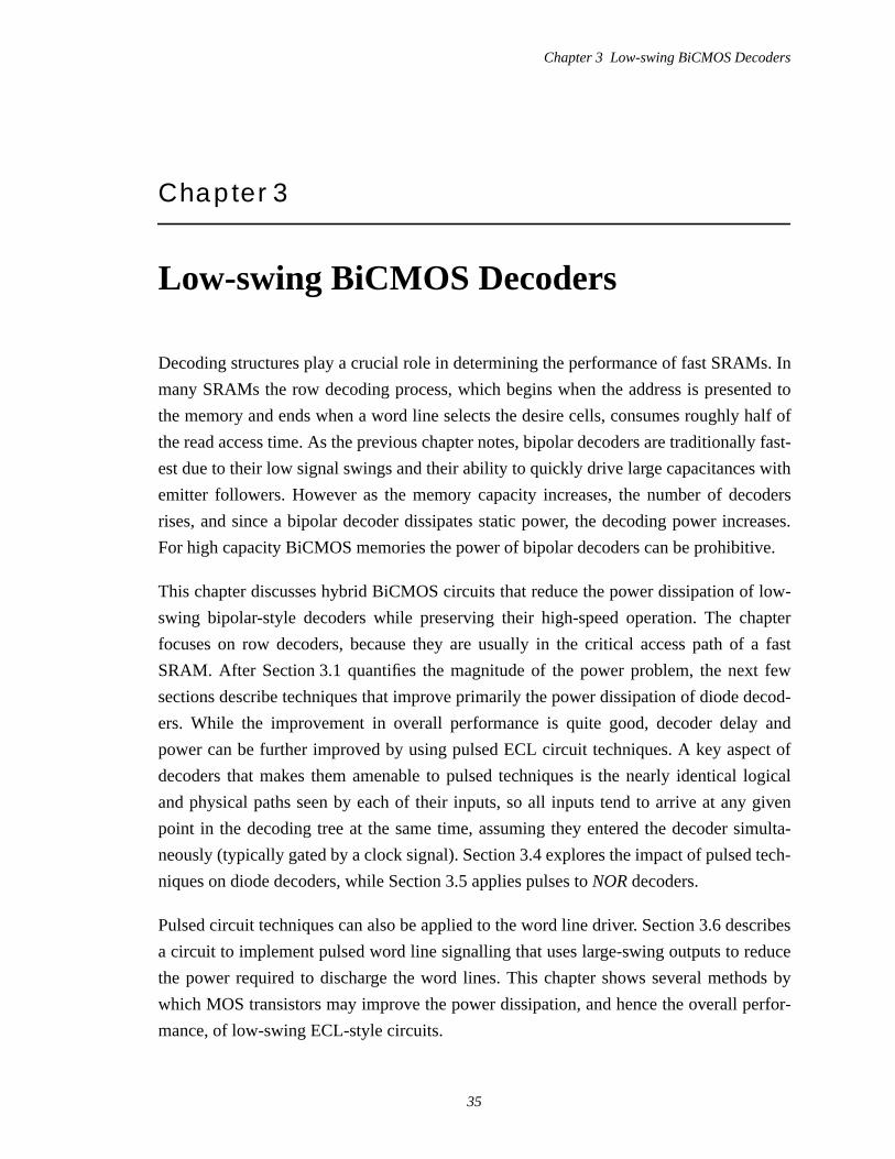
Chapter 3 Low-swing BiCMOS Decoders
35
Chapter 3
Low-swing BiCMOS Decoders
Decoding structures play a crucial role in determining the performance of fast SRAMs. In
many SRAMs the row decoding process, which begins when the address is presented to
the memory and ends when a word line selects the desire cells, consumes roughly half of
the read access time. As the previous chapter notes, bipolar decoders are traditionally fast-
est due to their low signal swings and their ability to quickly drive large capacitances with
emitter followers. However as the memory capacity increases, the number of decoders
rises, and since a bipolar decoder dissipates static power, the decoding power increases.
For high capacity BiCMOS memories the power of bipolar decoders can be prohibitive.
This chapter discusses hybrid BiCMOS circuits that reduce the power dissipation of low-
swing bipolar-style decoders while preserving their high-speed operation. The chapter
focuses on row decoders, because they are usually in the critical access path of a fast
SRAM. After Section 3.1 quantifies the magnitude of the power problem, the next few
sections describe techniques that improve primarily the power dissipation of diode decod-
ers. While the improvement in overall performance is quite good, decoder delay and
power can be further improved by using pulsed ECL circuit techniques. A key aspect of
decoders that makes them amenable to pulsed techniques is the nearly identical logical
and physical paths seen by each of their inputs, so all inputs tend to arrive at any given
point in the decoding tree at the same time, assuming they entered the decoder simulta-
neously (typically gated by a clock signal). Section 3.4 explores the impact of pulsed tech-
niques on diode decoders, while Section 3.5 applies pulses toNOR decoders.
Pulsed circuit techniques can also be applied to the word line driver. Section 3.6 describes
a circuit to implement pulsed word line signalling that uses large-swing outputs to reduce
the power required to discharge the word lines. This chapter shows several methods by
which MOS transistors may improve the power dissipation, and hence the overall perfor-
mance, of low-swing ECL-style circuits.

3.1 Bipolar Decoder Power Dissipation
36
3.1 Bipolar Decoder Power Dissipation
A fundamental restriction in SRAM design is that no more than one word line should ever
be simultaneously active in any bank; since most SRAM cells are selected by a high level
on their word line, this implies that all but one of the word lines must be low at any given
time. In ECL-style signalling, the word line driver is often similar to Figure 3-1, and as in
other ECL circuits, the decoder must pull current from the load resistorRDec to keep its
output low.RDec is usually part of the decoder gate itself, and since all but one of a decod-
er’s outputs are zero, the amount of current required for the decoders themselves is simply:
(3-1)
whereNRows is the number of rows in the decoder andVSwing is the decoder (and thus
nearly the word line) voltage swing.
For single-array designs, the number of decoders therefore scales withNRows and thus as
the square root of the memory size. The power of low-swing bipolar decoders increases
more rapidly than the number of decoders, becausefan-in andfan-out considerations both
require increasing power dissipation per decoder. Since the decoder rise time is the pull-up
resistance times the node capacitance, which is dependent on the input
devices in each decoder,RDec must decrease as the gatefan-in increases to maintain a
IDec
NRows 1−( ) VSwing
RDec=
RDec
Word Line 0Decoder
Word Line N
Discharge
Word Line Driver
Figure 3-1 Simplified Word Line Driver
log2NRows

3.2 Pre-decoding for Diode Decoders
37
given delay. In order to maintain constant decoder swings, the current per decoder must
therefore rise. Also, as the number of cells per word line increases, the pull-down current
on this line also needs to increase to maintain the delay. UnlessRDec is decreased by the
same proportion, the current gain of the Darlington-connected word line drivers will need
to increase, which can lead to ringing in their transient response. Thus, increasing the
decoderfan-out may necessitate increased decoding power as well.
For banked designs that maintain constant bank sizes as the memory size increases, the
power scaling is much worse. Since doubling the memory capacity implies doubling the
number of banks, the total number of decoders increases linearly with the memory capac-
ity. While this is not a problem for CMOS decoders, which dissipate very little power
when inactive, doubling the number of bipolar decoders doubles the power dissipation.
Because power dissipation and sensing considerations often dictate that only one word
line should be high in the entire memory, all of the bits that determine the active bank must
also affect the row decoder. The row decoder therefore has input
bits, which is more than a single square array; for instance, for a quadrupling of the mem-
ory size, the banked decoders each get two more inputs while the row and column decod-
ers of a square array each get a single extra input. The reason for this is simple: the banked
design must perform more decoding to select among the shorter word and bit lines. Thus,
the fan-in of the bank decoders increases more rapidly than that of the square decoders,
and thus the power per decoder for equal delay rises more quickly as well. The decoding
power of a banked design therefore increases super-linearly with the memory capacity.
Many banked designs improve the situation somewhat by increasing both the bank size
and the number of banks as the memory capacity increases. While this technique might
limit the super-linear increase in power, even a linear increase is unacceptable. The follow-
ing sections attack this problem. By reducing thefan-in of the final decoder gate, the
decoder power need not increase as rapidly with increasing memory size. By dynamically
varying the decoder resistance, unselected decoder banks need not spend as much power as
the selected bank. And by pulsing the word line discharge current, the Darlington does not
need to fight the discharge current, so the decoder may have a higher driving resistance.
3.2 Pre-decoding for Diode Decoders
Most CMOS memories use pre-decoding to reduce thefan-in (and thus improve the
speed) of their decoders, and a similar technique can be used in bipolar diode decoders. In
log2 NRowsNBanks( )

3.2 Pre-decoding for Diode Decoders
38
a conventional diode decoder each address line is driven by a push-pull buffer (Figure 3-2)
that steers a currentIAdBuf into each unselected address line viaQ1 andQ2 [18]. The
inverter formed byQ3, Q4 and the emitter followers serves primarily to rapidly charge
the rising address line. Pre-decoding the address lines is readily accomplished by increas-
ing the complexity of the pull-up gate and removing the current switches in the pull-down
path.
A pre-decoding address buffer is shown in Figure 3-3. In this buffer, one of the two inputs
is level-shifted and then these two inputs are used to feed four different two-level series
stacks, which generate the four possibleAND combinations of two inputs: , ,
, and . This pre-decoding reduces the number of diodes in each decoder by a
factor of two, since each address line represents a two-bitAND. Each gate output has a
discharge current of 2IAdBuf/3, so that the three low address lines together pull the same
2IAdBuf from the decoder array as do two bits’ worth of the traditional address buffers.
These outputs have a somewhat faster fall time than the traditional ones, since each line
uses two thirds as much pull-down current to drive half as many diodes and two thirds as
much wire width (since the currents are much too high for minimum-width wires).
Pre-decoding improves the overall decoding speed at the expense of some stacked gates
(with an associated access penalty that is smaller than the improvement from reducing the
number of diodes in each decoder) and about a third more current, since the high output
now wastes pull-down current that was previously steered away. However, this lack of
A0
Q4Q3
Q2Q1
IAdBuf
In0
Ref
A0Ref
Figure 3-2 A Push-pull Address Buffer
A0A1 A0A1A0A1 A0A1

3.3 Diode Decoder with Switched PMOS Load Resistor
39
current steering in the pull-down current provides an opportunity for further performance
enhancements, which are described in the next few sections.
3.3 Diode Decoder with Switched PMOS Load Resistor
In a memory incorporating multiple banks of row decoders, current could conceivably be
steered into only the decoders of the selected array, saving the power that would otherwise
go into unselected arrays. This would make the decoder more CMOS-like, since unse-
lected banks would dissipate little power. Unfortunately, the unselected diode decoders
would then all float high because the current required to keep them low was removed. All
the associated word lines would therefore float high as well, which is not allowed. Even if
this was acceptable, the current required to rapidly discharge these heavily-loaded lines
upon re-selection of the array would dwarf the power savings of partial array activation.
Thus, for such a scheme to be effective requires a diode decoder that can be powered
down without letting its output float high. One method of accomplishing this function is to
replaceRDec with a variable load formed by a PMOS device.
With a variable PMOS load element, such a decoder has two distinct states. In the unse-
lected state, the decoder control circuits set the PMOS gate potential so the equivalent
resistance of the PMOS device is relatively high, which minimizes the current required to
keep the decoder output low. In the selected state, the PMOS load approximates the resis-
tance ofRDec, so the modified decoder switches as rapidly as the original decoder.
2/3 IAdBuf
In0A0A1
In1
A0A1
A0A1
A0A1
Figure 3-3 A Pre-decoding Address Buffer

3.3.1 Basic Operation
40
Achieving rapid bank selection without vulnerability to process and temperature variation
requires careful PMOS device sizing and reference level design. Furthermore, the reduced
decoder current provided by the switched PMOS loads exposes address line parasitics that
can slow the access. This section discusses these matters in detail, and shows that after
addressing them large power savings are possible.
3.3.1 Basic Operation
Figure 3-4 depicts a diode decoder with a power-down input. The standard resistor load in
the diode decoder is replaced by a PMOS transistorP1, allowing the resistance of the load
to be adjusted. In the selected (powered up) state, each decoder in the bank will have a
high level onBankSelQ and a low level onBankSelP. The low level ofBankSelP is set
by Q3 and makes the resistance ofP1 the desired (low) value for normal decoder opera-
tion.
A decoder is deselected by pullingBankSelP high viaQ2 to VCC – VBE, which greatly
increases the resistance ofP1. Very little current is then required to keep the decoder out-
puts low; this is readily provided byBankSelQ, which transitions downward upon dese-
lection. BankSelQ also guarantees that no word lines are high in unselected banks and
provides some safety margin during selection transitions (i.e. in caseP1 turns on slightly
A0 ANA0 AN
Address
Q3
P1P2
Q1
Decoder Cell
BSQBSP
PMOS Ref
Q2
LinesBank
Selectors
Figure 3-4 A PMOS Load Diode Decoder

3.3.2 Switched PMOS Load Design Considerations
41
before the decoder inputs begin pulling current). TransistorP2 is a very weak device to
provide a path toVCC in caseBankSelP ever turnsP1 completely off.P1 is sized to min-
imize the required gate voltage swing for selection without greatly increasing the decod-
er’s parasitic capacitance, so as to minimize any delay penalty for the switched load
device.
3.3.2 Switched PMOS Load Design Considerations
The switched PMOS load, if it is to be a useful replacement for a simple resistor, must
have similar performance characteristics in the “on” (low resistance) state. These charac-
teristics are demonstrated by first describing the PMOS device sizing versus selection
swing tradeoffs and then comparing the switching performance of the PMOS load with a
resistor.
If the PMOS load is operated entirely in thelinear region, where its drain currentIDrain is
more dependent onVDS, then its load characteristic over its operating region will more
closely approximate the resistor it is designed to mimic. This is readily demonstrated by
considering the load characteristic of the resistor (using Ohm’s Law):
(3-2)
and of the PMOS device in the linear region of operation ( ) [39]:
(3-3)
Since both equations specify zero current when the output is high (i.e.VLoad = VDS = 0),
the selection voltage and device ratio are set such that the PMOS device supplies the same
current as would the resistor when the output is low (i.e.VLoad = VDS = VSwing). Combin-
ing the above equations:
(3-4)
ILoad
VLoad
RDec=
VGS VTh− VDS>
ILoad IDrain KpWL
VGS VTh−( ) VDS
VDS2
2−= =
VGS VTh− 1
KpWL
RDec
VSwing
2+=

3.3.2 Switched PMOS Load Design Considerations
42
which is valid provided the PMOS device is linear, i.e.
(3-5)
or equivalently
(3-6)
Assuming that the PMOS load deselection is accomplished as in Figure 3-4, node
BankSelP will be unselected atVCC – VBE and selected atVCC – |VGS|. This selection
swingVSel should be minimized for low selection delay, but reducingVSel implies increas-
ing W/L, which increases PMOS device parasitic capacitances and thus lengthens the load
rise and fall times. Also, reducing the selection swing to small values can push the PMOS
device into saturation. Figure 3-5 depicts simulated load lines for three different PMOS
sizes and the selection swings required to make each mimic a 2-KΩ RDec with VSwing of
0.8V.
Saturation greatly increases the differential resistance of the load atVCC – VSwing, and
thus makes the low output voltage very sensitive to the load current, and therefore more
sensitive to device mismatch. Furthermore, the increasing load resistance can lengthen the
tail of theRC-dominated falling output voltage transition. These two factors make satu-
rated loads undesirable for traditional ECL-style gates, where the current into the load is
fixed. However, these factors do not substantially degrade a diode decoder load, since the
exponential current-voltage relationship of the input diodes rapidly increases the pull-
down current into the load such that the output voltage follows the input voltage; similarly,
the diode gate is relatively insensitive to device mismatch because the low output voltage
is determined as the low input voltage plus the diodeVBE. In fact, the input diodes so com-
pletely dominate the falling transition that one might consider intentionally choosing a sat-
urated PMOS load for diode decoders, since the saturated load pulls up more quickly than
a linear PMOS load. However, increasing the PMOSW/L to reach saturation can increase
the device parasitics (on the decoder node) enough to erase the speed advantages of a
reducedBankSelP swing, as well as increasing the current required to rapidly discharge
BankSelP. The PMOS loads in this thesis are designed to haveVSel nearly equal to
standard ECL logic swings (i.e. about 0.8V). WithVSwing, VBE, and |VTh| all nearly the
VGS VTh− VSwing>
1
KpWL
RDec
VSwing
2>

3.3.2 Switched PMOS Load Design Considerations
43
same level, this implies that the switched PMOS load is designed to be on the edge of sat-
uration.
The selection swing should not increase substantially with variation in manufacturing pro-
cess parameters or operating temperatures, in order to avoid losing the speed advantages
of low-swing signalling. Circuit simulations indicate that a 1.1-VVSel is achievable even
under worst-case processing conditions at room temperature.VSel must increase with tem-
perature, but its increase is no worse than that of the other ECL signals in such a design,
which are typically proportional to absolute temperature (PTAT). The variation of the
required selection swing over process and temperature variation appears as Figure 3-6.
Since the worst-case swing is only 220mV greater than the nominal swing, the PMOS
load selection swing always stays fairly small (and thus quick).
The transient behavior of the switched PMOS load closely matches that of the simple
resistor, especially for diode decoders. Figure 3-7 shows circuit simulation of 0.4-mA
4-input diode decoders and ECL inverters with resistor or PMOS loads, each driving a
1.6-mA emitter follower; the PMOS loads are the 30-µm devices from Figure 3-5, with
nominalVSel of 0.89V. The diode decoders begin their transitions early because they do
0.0 0.5 1.0 1.5 2.0Load Element Voltage (V)
0.0
0.2
0.4
0.6
0.8
1.0
Cur
rent
(m
A)
W=15µm, VSel =1.56VW=30µm, VSel =0.89VW=60µm, VSel =0.54V2-KΩ Resistor
Figure 3-5 PMOS Load Characteristics

3.3.3 Reference Generation
44
not wait for their inputs to cross a threshold as do the inverters, and they deliver less than
0.8-V swings because they are driven with the same voltage input as the inverters (for pur-
poses of comparison only) and so diodeVBE variations between high and low currents
decrease the swing. The rising transitions are very comparable for both load devices,
regardless of gate type, while the falling transitions for the diode decoders are similar
because the diode’s exponential current forces these transitions to closely follow their
input. The falling PMOS load inverter transition requires about 70ps longer to reach the
swing midpoint than does the resistor load due to both larger parasitics and larger device
currents at intermediate voltages, as was noted above. Section 3.5 discusses ECLNOR
gate circuits using switched PMOS loads that are tolerant of this added delay.
3.3.3 Reference Generation
The power savings potential offered by the switched PMOS load is realized only if the
selection node swings are rapidly delivered. Because switching a node between two arbi-
trary and well-controlled voltages is difficult, the PMOS load switches between a refer-
ence-controlled active (low) level and an inactive (high) level of oneVBE below VCC.
Using a reference allows the use of simple wired-or selection drivers, which simply need
0 25 50 75 100 125Temperature (C)
0.5
0.6
0.7
0.8
0.9
1.0
1.1
1.2
1.3
1.4
1.5V
olta
geTypicalFastSlowPTAT Swing
Figure 3-6 PMOS Load Gate Swing Over Process and Temperature

3.3.3 Reference Generation
45
to guarantee that their swing is larger than the selection swing, so that their low value is
below the reference and thus the reference will set the overall selected voltage.
A circuit to generate a reference oneVBE above the desired selection level is depicted in
Figure 3-8. Identical current sources pull the active decoder currentIDec from both a rep-
lica of the PMOS load element (selectableP1 in parallel with weakP2) and a resistor
RDec with the desired load resistance. The drops across each load are shifted down byD1
andD2 (to prevent saturation ofQ1 andQ2) and are compared by the feedback amplifier
formed byQ1, Q2, P3, andP4 to generate a voltagePMOSRef that is oneVBE (via Q3)
above the gate voltage required to make the load drops equal. PMOS current-mirror loads
are used in the amplifier both to increase the gain and to make the load characteristics
track those ofP1 and thus reduce the offset of the amplifier. The second amplifier is con-
nected as a unity-gain buffer and serves to isolate the internal reference nodes from
switching transients occurring from the use of the buffered referencePMOSRefBuf. The
-2.0
-1.5
-1.0
-0.5
0.0
Vol
tage
(V
)
0.0 0.1 0.2 0.3 0.4 0.5 0.6 0.7 0.8 0.9 1.0Time (ns)
PMOS Load Inverter
Resistor Load Inverter
PMOS Load Decoder
Resistor Load Decoder
InputRising Falling
Figure 3-7 Gate Switching Waveforms for PMOS Loads

3.3.4 Address Line Sharing
46
second amplifier uses a bipolar current switch and PMOS current-mirror loads, like the
first amplifier. Circuit simulations indicate that the reference generator has excellent sta-
bility in response to both transient supply variation and varying load current on
PMOSRefBuf, if compensation capacitance is added to nodePMOSRef.
3.3.4 Address Line Sharing
Reducing the power required by the diode decoder creates the new problem of driving the
high-capacitance address lines. In a conventional diode decoder the current that keeps the
decoders low is proportional to the number of decoder gates. Thus, the current to capaci-
tance ratio is constant. However, by powering down most of the decoders only the current
is reduced — the total capacitance is still proportional to the number of decoders.
To reduce this problem, each bank can have its own set of address lines, and therefore
minimize the loading on the (segmented) address lines. To continue to save power, only
one set of address lines should be powered at a time, so the bank selection circuitry should
steer the pull-down current into the selected bank’s address lines. Since the pre-decoding
address buffers do not themselves use any current steering in the pull-down path, there is
room for at least one level of steering here. However, if the current is steered among
NBanks banks, there may not be enough room for a stacked (i.e. tall) current
tree so one stage of bank address decoding gates may be needed to provide select signals
for a one-level (i.e. 1-of-NBanks) current-steering gate; this additional level of gates delays
the access.
P3P4
IDec
Q2Q1
Q3
D1
RDec
D2
IDec
P1P2
+
–
PMOSRefBufPMOSRef
Figure 3-8 PMOS Load Reference Generator
log2NBanks
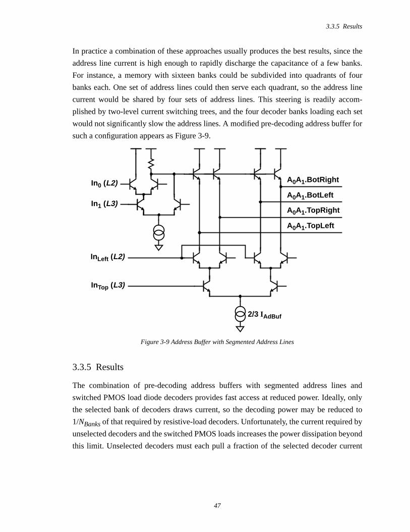
3.3.5 Results
47
In practice a combination of these approaches usually produces the best results, since the
address line current is high enough to rapidly discharge the capacitance of a few banks.
For instance, a memory with sixteen banks could be subdivided into quadrants of four
banks each. One set of address lines could then serve each quadrant, so the address line
current would be shared by four sets of address lines. This steering is readily accom-
plished by two-level current switching trees, and the four decoder banks loading each set
would not significantly slow the address lines. A modified pre-decoding address buffer for
such a configuration appears as Figure 3-9.
3.3.5 Results
The combination of pre-decoding address buffers with segmented address lines and
switched PMOS load diode decoders provides fast access at reduced power. Ideally, only
the selected bank of decoders draws current, so the decoding power may be reduced to
1/NBanks of that required by resistive-load decoders. Unfortunately, the current required by
unselected decoders and the switched PMOS loads increases the power dissipation beyond
this limit. Unselected decoders must each pull a fraction of the selected decoder current
Figure 3-9 Address Buffer with Segmented Address Lines
InTop (L3)
A0A1.TopLeft
InLeft (L2)
A0A1.TopRight
A0A1.BotLeft
A0A1.BotRight
2/3 IAdBuf
In0 (L2)
In1 (L3)

3.3.5 Results
48
IDec from their PMOS load to maintain a low output; the current required is simply
(3-7)
whereROff is the equivalent resistance of the unselected decoder load. For systems with a
large number of banks, the unselected decoder power is often comparable to the selected
decoder power, because there are many more unselected decoders andROff/ROn ratios
much larger than ten require large selection swings.
The high capacitance on the bank selection nodeBankSelP also increases the decoder
power. Because the transition ofBankSelP needs to be quick for low decoding delay, the
capacitance of the PMOS gate terminals require a large discharge current. This discharge
current must equal about a quarter of the load current supplied by the PMOS transistor
(i.e. IDec) for fast selection, so if simple static sources supply the discharge currents then a
substantial amount of the power saved by switching the decors will be lost. A single dis-
charge source may be steered to the selected bank, since only oneBankSelP drops per
access. However, as described in Section 3.3.4, this requires anAND of the bank
addresses, which may either require too many levels of series gating to avoid saturation or
an extra stage of ECL gates (and thus extra delay) to generate select signals. Like the seg-
mented address line drivers, a two-level current switch provides a hybrid solution that
reduces the power by a factor of four. Even with reduced discharge current each follower
on the wired-or selection lines needs the ability to charge thatBankSelP by itself and
therefore the gates need sufficiently low load resistance to avoid emitter follower oscilla-
tion problems. Therefore, the current in the ECL gates that drive these followers is about
one quarter of theBankSelP discharge current.
An example shows the impact of the standby and control current on the power dissipation.
In a sixteen-bank design, the ideal power dissipation is 1/16 (6.25%) that of traditional
resistive decoders. If the PMOS loads change resistance by a factor of ten, then the fifteen
unselected banks draw 9.4% additional power. For theBankSelP nodes, with one quarter
of IDec per load and two levels of current steering, an additional 6.25% is required in dis-
charge current sources; with a factor of four between discharge currents and the gates that
drive the wired-or followers, 6.25% more current is needed. In this example, the ideal
power ratio of 6.25% increases to 28.15% once the non-idealities are considered. While
this is less than one-third of the original power, it is about five times the ideal value.
IUnsel IDec
RDec
ROff=

3.4 Pulsed Diode Decoders
49
In conclusion, the switched PMOS load offers enticing power savings for diode decoders
by allowing unselected banks of decoders to keep their outputs low with much less static
current while providing fast access in the selected bank. However, the substantial power
required by the controlling circuitry reduces the savings significantly. A new approach is
therefore desired that minimizes the control power without sacrificing access time. The
next two sections describe techniques that can achieve this goal.
3.4 Pulsed Diode Decoders
Many fast CMOS SRAMs use synchronization signals (i.e.clocks), that allow designers to
minimize access delay and power. Starting from a low-power reset state, synchronous
SRAMs selectively enable power-consuming circuits, based upon the requested address.
Once the access is complete, the SRAM resets its internal signals to their inactive state,
thus preparing for the next access. The power savings come both from activating circuits
for only part of the access cycle (i.e. when they need to be active) and from only enabling
the circuits that may possibly switch; for example, a multi-bank design would only enable
the decoder bank that is selected by the bank address. The delay reduction results prima-
rily from separating the selection and reset circuitry, so each path can be tuned for opti-
mum speed, as was discussed in Section 2.2.2.
Bipolar SRAMs, as well as those BiCMOS SRAMs with mostly-bipolar access paths, tend
not to have clocks because of the basic ECL gate structure, which uses passive load resis-
tors to pull up gate outputs, and thus requires substantial static current to keep an output
low. A low-power ECL reset state would thus have all outputs high, which is unacceptable
for signals such as word lines that are active high. This thesis describes new techniques
that utilize clocks with active loads to reduce both delay and power dissipation of
BiCMOS SRAMs. These techniques succeed, in much the same way as CMOS circuit
techniques, by reducing power dissipation in a reset state, quickly selecting power-con-
suming circuits to accomplish the access, restricting signal transitions to speed logic gates,
and building separate reset paths to speed both selection and reset transitions.
While there are many ways to use clocks in SRAMs, this thesis is concerned with tech-
niques that use a single input clock (which guarantees that all input transitions occur
simultaneously) and from this signal generate controlled pulses that select specific circuits
for activity, remain active long enough for these circuits to select the following stage of
circuits, and then cause their circuits to reset when they go inactive. At each stage of the

3.4.1 Basic Operation
50
access, new pulses are generated from the immediately previous stage, with timing skew
equal to the stage delay. In order to minimize the overhead associated with controlling
these pulses, the pulses are typically part of the data stream; in other words, since all inter-
nal signals begin in an inactive (i.e. reset) state, stageN is activated by the active transi-
tions of signals from stageN – 1 and stageN activates stageN + 1 in turn.
This section applies pulsed techniques to diode decoders, while later sections extend these
techniques to bothNOR decoders and other stages of a BiCMOS SRAM. Pulsing a diode
decoder improves its performance primarily because all inputs to the selected decoder rise
simultaneously, and therefore the junction capacitance of the diode provide charge that
speeds the rising transition. The next subsection discusses adding explicit capacitance to
further speed the decoder; the effects of the injected charge on unselected decoders lead to
the use of an MOS capacitor to reduce the unwanted charge. This section closes with a
summary that questions the usefulness of the capacitively-assisted decoders, given the
power of the extra circuitry needed to control them.
3.4.1 Basic Operation
A pulsed diode decoder may be built just like the traditional diode decoder of Figure 2-10.
The differences are in the address buffer that drives the decoder, and the word line driver
that capacitively loads it. The decoder begins its access with all its input lines low, so all
the word lines in the system start low and thus no memory cells are selected. The address
buffers pulse (i.e. raise) the selected address lines to begin the access; the selected decoder
therefore sees all of its inputs rise at once, which forces the decoder to charge more
quickly than when only one input transitions. The base-emitter diode capacitances supply
charge to hasten the transition, whereas in the traditional decoder only one input might rise
and thus the capacitance of the other inputs’ diodes would hinder the rising transition. The
access is further improved by removing the large static currents from the Darlington word
line drivers. This change helps by reducing the total amount of base charge required to
make the Darlington charge the word line, thus further reducing the current required
through the load resistor to charge the decoder. The word line driver employs a separate
reset path to discharge its output, which is discussed in a later section.
Circuit simulations of the selection delay through the diode decoder and word line driver
circuitry versus decoder current appear as Figure 3-10. Delays are compared for three

3.4.1 Basic Operation
51
circuit configurations:
• Traditional decoders with static word line discharge
• Pulsed decoders with static word line discharge
• Pulsed decoders with pulsed word line discharge
The data indicate that at an example current of 400µA, pulsed decoder signalling delivers
a rather modest 120-ps (15%) gain by itself, but also enables the use of pulsed word line
circuitry that delivers an additional 280-ps gain for an overall selection delay reduction of
50% for these two stages. The figure clearly indicates that reducing the required Darling-
ton base charge can produce fast decoders at much lower decoder current. This might lead
one to wonder how little static current would be enough to provide fast access, if some
way were found to dynamically dump the base charge into the decoder. The next section
investigates adding explicit capacitance to the decoder inputs to supply this charge.
100 200 300 400 500 600 700 800Active Decoder Current ( µA)
0.2
0.4
0.6
0.8
1.0
1.2
1.4
Del
ay (
ns)
Trad. Signalling / Passive Pull-DownPulsed Signalling / Passive Pull-DownPulsed Signalling / Active Pull-Down
Figure 3-10 Advantages of Pulsed Signalling for Diode Decoders

3.4.2 Capacitively-pulsed Diode Decoders
52
3.4.2 Capacitively-pulsed Diode Decoders
Increasing the parasitic capacitance of the input diodes increases the amount of charge
transferred to the decoder and provides fast rise times with lower static decoder current
(i.e. higherRDec). While adding capacitance normally slows switching speed, the circuit
of Figure 3-11 is different because the capacitorsfeed the input signalsforward (i.e.
directly) to the decoder without requiring any device switching norRC delays; on the
selected decoder all the inputs rise at the same time so there isNInputsCIn working to
charge the decoder together, whereNInputs is the number of decoder inputs. Because the
source of the feed-forward charge is a change in the voltage acrossCIn, the address lines
must swing more that the internal decoder node. Circuit constraints limit the realizable dif-
ference between these swings to be fairly small, soCIn must be relatively large in order to
deliver the required Darlington base charge.CIn is large enough that it requires less area to
implementCIn as a separate component rather than simply increasing the area of the input
diodes.
The chief drawback of increasingCIn is the disturbance created on unselected decoders
that connect to selected address lines. A decoder connected to only one unselected address
line has a large amount of charge dumped onto it as the selected lines rise, since the
change in voltage across its capacitors will be nearly the entire address line swing. This
undesired charge raises the internal decoder node, which in turn raises the unselected
address lines as the voltage across the decoder diodes increases. Pulsing extra current from
RDec
AddressLines
ToWordLineDriver
CIn
CIn
Figure 3-11 A Capacitively-Pulsed Diode Decoder

3.4.2 Capacitively-pulsed Diode Decoders
53
unselected address lines while the selected lines are rising fights the undesired charge and
prevents the unselected lines from rising. However, since there are so many unselected
decoders the undesired charge is large. Using nonlinearCIn reduces the charge dumped
onto unselected decoders, thus reducing both the rise in barely-unselected decoders and
the power spent in keeping the unselected address lines low.
Resetting a capacitively-pulsed diode decoder requires pulling the selected lines low,
which restores the charge on the feed-forward capacitors. Quickly restoring this charge
requires much more current than the static decoder current, so pulsed reset currents are
appropriate. The selected decoder rapidly resets due to the feed-forward input capacitors
and the exponential current characteristics of the input diodes.
Raising the decoder output using feed-forward capacitance requires that the address lines
rise further than the decoder output so the voltage acrossCIn decreases. For a fixed
decoder swing, the extra address line swing is therefore roughly inversely proportional to
CIn, but neither value can be arbitrarily large without other penalties. Because the decoder
high level needs to be essentiallyVCC (so the high word line level does not degrade) and
because the inactive (reset) level on the address lines is simply oneVBE below the decoder
low level, increasing the address line swing over the decoder swing requires a selected
address line to be higher thanVCC – VBE, which is difficult to accomplish with emitter fol-
lowers. Some amount of excess swing is available in practice, since driving the high input
capacitance of the decoders tends to make the address buffer emitter follower overshoot its
static selected level a bit. However, the amount of overshoot is dependent on high fre-
quency characteristics of the BJT and is therefore very sensitive to process variation. The
intrinsic difference in the input diodeVBE between high current (unselected decoder) and
low current (selected decoder) levels readily delivers about 100mV of excess swing; to
achieve enough charge with a small voltage change requires relatively largeCIn.
However, largeCIn increases the disturbance of unselected decoders that are connected to
selected address lines. For a decoder connected to only one unselected address lines, a
total charge of almost (NInputs – 1)CIn ∆VAdLine is dumped into the decoder, where
∆VAdLine is the swing on the address lines; in order to keep the unselected word line from
rising, this charge must discharge through the unselected input diode. A better solution is
to use a nonlinear capacitor — a device whose capacitance increases with the applied volt-
age. Such a capacitor could have a relatively large equivalent value for the selected
decoder, where the terminal voltage change is small, and a relatively smaller equivalent
value for unselected decoders, which have∆VAdLine terminal changes.

3.4.3 NMOS Capacitor Diode Decoders
54
3.4.3 NMOS Capacitor Diode Decoders
An MOS transistor can implement a nonlinear capacitor, since with the source and drain
terminals shorted together the device has a small capacitance from gate to (source-drain)
whenVGS < VTh, due to the lack of any conducting channel, whereas onceVGS > VTh a
channel forms under the gate and the equivalent capacitance rises substantially. In order to
utilize this non-linear behavior for a diode decoder, appropriate driving circuitry is
required to ensure that the voltage drop across the MOSFET at the reset state is just above
the device threshold so that when the terminal voltage decreases, most of the stored charge
will dump onto the decoder internal node quickly and then the rest of the voltage change
will dump relatively little charge.
A diode decoder using such a capacitor appears as Figure 3-12. The variable level shifters
(one per address line) sets the resetVGS on the NMOS capacitors to a few hundred milli-
volts above their (body-effect altered)VTh; they must be variable because the NMOSVTh
does not track the bipolarVBE nor ECL swings over process and temperature variations.
Circuit simulations indicate that the MOS capacitor reduces the charge dumped into unse-
lected decoders and thus improves decoder performance in two ways. First, for a 6-input
decoder with 100-µA current per decoder and 100-fF capacitance per input the undesir-
able bump in barely-unselected decoders is reduced relative to linear capacitors from
430mV to 280mV (i.e. by 35%) without any increase in delay at an address line swing of
RDec
AddressLines
ToWordLineDriver
Figure 3-12 A NMOS Capacitor Pulsed Diode Decoder

3.4.3 NMOS Capacitor Diode Decoders
55
1.2V. Second, the drop in total injected charge reduces the discharge current requirements
on the address lines enough that a 6-bit (64 cell) row decoder constructed from the above
gates requires 40% less average address line current than it would with linear capacitors,
at a cycle time of 2ns.
The variable level shift required by the NMOS capacitors may be implemented by a mod-
ified VBE multiplier circuit. The basicVBE multiplier circuit, as well as a possible modifi-
cation to give it the desired variable characteristic, appear as Figure 3-13. The traditional
VBE multiplier [22] acts as a two terminal device with a programmable diode characteris-
tic (i.e. an adjustableVBE). As the terminal voltage differenceVMult rises from zero, cur-
rent will flow entirely through the resistors until the voltage drop acrossR1 approaches
VBE andQ1 turns on. At this point the base-emitter junction will clamp theR1 drop to
VBE and, as long as the base current ofQ1 remains small compared withVBE/R1, the cur-
rent throughR2 will closely match that ofR1 and hence
(3-8)
for the range of operation where the terminal currentIMult satisfies
(3-9)
ReplacingR1 with a variable resistor (NMOS deviceN1 in the Figure) allows the pro-
grammable diode voltage to be dynamically adjusted by a control signalResCntl. The
equivalent resistance ofN1, and hence the diode voltage, are determined both byResCntl
VMult VBE 1R2R1
+( )=
VBE
R1IMult
βVBE
R1«<
R2
N1
Q1
R1
+
–
VMult
IMult
ResCntl
Figure 3-13 An AdjustableVBE Multiplier

3.4.4 Summary
56
and by the source voltage ofN1, since bothVGS and the body-effect dependent value of
VTh alter N1’s current. For a fixedResCntl, this implies that the NMOS resistance
increases as the source voltage increases so thus the programmable diode voltage
decreases. This feature is useful for the NMOS capacitor decoder since it makes the vari-
able source voltage decrease as the address lines rise, thereby providing a larger input
swing on the capacitors than on the diodes and thus increasing the voltage chance across
the capacitor. The voltageResCntl is set by a replica circuit to forceN1’s resistance in the
reset state such that the drop across the NMOS capacitors is a few hundred millivolts
above theirVTh.
Circuit simulations indicate that the adjustableVBE multiplier performs quite well in rap-
idly charging the capacitor input lines. However, the limited current range offered by a
VBE multiplier creates problems for this application because of the large variation between
the standby (reset) and active address line currents. In order to generate the desired diode
voltage at the low reset current the resistance values must be relatively large, but large
resistance increases the charging delay of the capacitors. Circuit simulations indicate that
the extra delays of aVBE multiplier over a simple diode withR2/R1 = 1/3 are about (30ps,
45ps, 70ps, 110ps, and 190ps) at active/static current ratios of (1, 2, 4, 8, and 16); since
these delays are in addition to the intrinsic base charging delay of a simple diode it is clear
that some of the delay performance gained in using capacitively-pulsed decoders is given
back in driving them.
3.4.4 Summary
Pulsed circuits show great promise for improving the delay and power performance of
diode decoders. While the single greatest delay improvement comes from freeing the ris-
ing word line driver from fighting a large static discharge current, the simultaneous rise of
the inputs presents an opportunity to use feed-forward capacitance to charge the Darling-
ton base at much lower static decoder current. With nonlinear NMOS capacitors the total
injected charge is reduced and thus the total decoder power improves as well. Figure 3-14
compares the decoder plus word line driver delays and average address line current for the
decoders discussed in this section. The simulated circuit implements a 1-of-64 diode
decoder, with each gate having 6 inputs. The first curve shows the delay of the pulsed
decoder of Section 3.5.1 as the static gate current is increased from 75 to 400µA per
decoder. The other curves show the delay curves for linear and NMOS capacitor decoders
as CIn varies from 10 to 150fF per input and as the gate current increases from 40 to

3.4.4 Summary
57
200µA. The NMOS delays are optimistic because they do not include the delay of theVBE
multiplier, which would add about 150ps to the times.
The figure shows that NMOS capacitor decoders are able to achieve low delay at much
lower static decoder current, and lower average power, than pulsed decoders without
capacitors. However, the NMOS decoders have higher delay for a given capacitor size that
linear capacitor decoders due to theVBE multiplier delays, albeit at substantially lower
power; the lack of a high value per unit area linear capacitor in most digital processes rule
out the linear decoder altogether.
The use of bank selection may be combined with these techniques to further reduce power
dissipation. A simple pulsed decoder might use a switched PMOS load, as was described
in Section 3.3, but the greatly reduced static current of the NMOS capacitor decoder does
not require such an approach. Instead, such a decoder dissipates most of its power charg-
ing the feed-forward capacitors, preventing unselected address lines from rising, and dis-
charging selected address lines so the goal in using banks is to prevent address lines from
switching. Since this approach requires segmenting the address lines so each bank (or each
5.0 10.0 15.0 20.0 25.0 30.0Average Decoder Current (mA)
0.30
0.35
0.40
0.45
0.50
0.55
0.60
0.65D
elay
(ns
)Pulsed With No C InLinear C In=10fFLinear C In=60fFLinear C In=150fFNMOS CIn=10fFNMOS CIn=60fFNMOS CIn=150fF
75
100
150
200
300
400
40 60 80 100200
Figure 3-14 Power/Delay Comparison of Pulsed Diode Decoders

3.5 Pulsed NOR Decoders
58
few banks) has its own set of lines the address buffers become more complex and may
require an extra delay stage to accomplish.
The extra complexity in generating the current pulses for unselected but active address
lines and the reset currents for selected diode and capacitor decoder inputs, coupled with
the extra delay in the address buffers, make the power savings offered by the NMOS
decoders difficult to achieve; in practice the speed and power performance of the pulsed
static decoders, in combination with switched PMOS loads, is quite adequate and much
simpler to achieve. The focus of the pulsed circuit investigation now shifts toNOR decod-
ers, where performance improvement impacts not only decoding structures, but also
generic ECL logic.
3.5 PulsedNOR Decoders
Many of the fastest reported bipolar and BiCMOS SRAMs utilizeNOR gate decoders for
the following reasons:
• Active-low inputs allow simple wired-or pre-decoding.
• Level-restoringNOR gate decouples input and output swings.
• Complementary outputs provide flexibility in building word line drivers.
BiCMOS access times as low as 1.5ns, and bipolar read delays of less than 1ns have been
reported usingNOR decoders [4 20]. The power of such decoders is not low; a recently
reported 256Kb BiCMOS SRAM [5] accesses in 2.4ns (1.5ns on-chip) but requires
almost 2A of current for the row circuitry alone. In order to build this type of access per-
formance in a reasonable-power large BiCMOS memory, theNOR decoder and word line
driver circuit power must be dramatically reduced. One method to accomplish the power
reduction is to create aNOR gate with a power-down state (like the improved diode
decoder of Section 3.3), and then only activate the decoders in the selected bank. Rather
than trying to steer the activeNOR gate current into the selected bank of decoders, a better
solution is a current source that may be powered down, so in the reset state no decoder
draws full power. Since the address lines of aNOR decoder do not share the decoder gate
currents, it is also important to reduce the address line power dissipation; a key benefit of
pulsed signalling forNOR decoders is that it is simple to determine when an address line
might transition and to supply the discharge current at only those times.

3.5.1 Basic Operation
59
This section discusses circuit techniques for building pulsed row access paths for
BiCMOS memories usingNOR decoders that minimize power dissipation without sacri-
ficing speed. After describing the basic pulsedNOR gate, the discussion focuses on the
design of a simple BiCMOS pulsed current source that overcomes many of the limitations
of previous designs. In combination with a new voltage regulator, this source delivers a
pulsed current that is largely independent of fast changes in the voltage supply levels and
that is selected using standard ECL voltage levels. The pulsed current source is used both
in the basicNOR gate and in the address buffers and line drivers to minimize their power.
The pulsedNOR banks require a bank selection signal to enable their current sources, but
generating this signal in a single gate delay is both required and challenging; a modified
diode decoder accomplishes this task nicely.
3.5.1 Basic Operation
A pulsedNOR gate for use in a decoder should draw very little current in the inactive
state, when its output is guaranteed to be low, and should have a much lower equivalent
load resistance in the active state so it can rapidly charge its output. A switched PMOS
device provides the desired load characteristics, but the pulsed gate also requires a vari-
able current source that switches between low inactive current and higher active current.
Figure 3-15 depicts such a gate, with switched PMOS loadP1 and switched current
source IDec. In the reset state, both of the bank selection signals,BankSelP and
BankSelQ, are inactive so the standby current sourceILeak needs to be large enough to
overpower an inactiveP1 and thus keep the decoder output at its low level. On a bank
selection, both the pulsed current source andP1 become active; on all decoders (except
the selected one)IDec must be large enough to keep the output low.BankSelQ must be
active slightly before and afterBankSelP to avoid generating glitches on the output.
IDec
P1 D1 R1
BankSelQ
In0
BankSelP
OR
NOR
ILeak
Figure 3-15 A Pulsed NOR Gate

3.5.2 Pulsed Current Source
60
Because the inactive resistance ofP1 is not well-controlled, diodeD1 sets the output low
level, which requires some excessILeak. D1 also allows the active PMOS load to be satu-
rated, which allows larger decoder output swings with smallBankSelP swings. The com-
plementary gate output may be supplied off a normal resistorR1, since no decoder save
the selected one steers current through this path, the complementaryOR output is
extremely useful for generating control signals for pulsed word line discharge circuits.
This decoder can provide delay performance nearly equal to a simpleNOR decoder at
much lower average power consumption, especially for multi-bank designs where only
one bank of decoders is ever activated at once. Note that the pulsedNOR gate has a longer
falling delay due to the switched PMOS load (as mentioned in Section 3.3.2), but this
delay is in the reset path, and thus does not increase the critical selection path delay
3.5.2 Pulsed Current Source
The design of a dynamic current source for such a decoder deserves careful consideration.
Much work has recently been devoted to active pull-down ECL circuits [40 41 42 43],
which reduce the power in their emitter followers by only activating pull-down currents
while the output is falling. The existing circuits, as well as the one required for this appli-
cation, must both handle the same fundamental problem: normal ECL signals are refer-
enced toVCC while current sources are referenced toVEE, so it is difficult to have normal
ECL signals turn on current sources due to the allowed variation inVCC – VEE. This volt-
age variation is at least 0.6V in most systems. Many solutions utilize capacitors to provide
a variable level shift that allows aVCC-referenced ECL level to control aVEE-referenced
current source, as depicted in Figure 3-16. However, capacitor-based solutions suffer from
two problems that make them unsuitable for this application. First, while the biasing net-
work that sets the size of the variable level shift can tolerate changes inVCC – VEE that
occur slowly with time, they cannot handle rapid changes in the supply voltages; this is
bad because pulsed current sources generate rapid changes in the die currents, and these
current changes generate rapid changes inVCC – VEE due to the inductance of the package
leads. In other words, capacitor-based pulsed current sources have trouble dealing with the
supply noise that they generate. Second, the capacitor solutions only output their peak cur-
rent for a limited time, since the charge stored on the capacitor leaks off while the current
source is active; this behavior is often acceptable for simply discharging the output node
of an emitter follower, where the logic gate itself keeps the emitter follower off once the
pulsed current drops off, but for pulsed logic gates the current needs to remain at the peak
level as long as the selection input is active so that the output voltages remain constant.

3.5.2 Pulsed Current Source
61
The pulsedNOR decoder therefore requires a new pulsed current source that is not based
on level-shifting capacitors.
Recent BiCMOS SRAMs have been constructed with on-chip voltage regulators to permit
3.3-V limited MOS devices to coexist with 5.2-V ECL circuits [38] by generating aVSS
for the memory cell array that isVCC – 3.3. This thesis proposes that this voltage regulator
be set such that building pulsed current sources from this supply be made simple; in other
words, theVSS generator should produce a voltage fourVBE plus the ECL signal swing
below VCC. With such aVSS, a pulsed current source may be simply constructed as in
Figure 3-17.
The operation of this source is simpler to understand with NMOS transistorN1 replaced
by a resistor. Assuming the selection signal isL3, it is low atVCC – 3VBE – VSwing, and
thus Q1 is on the edge of turning on. As the selection signal rises,VSwing is gradually
impressed across the resistor and thusVSwing/R flows through the current source. The
Base
CntlIPulse
VEE
VCC
Pulsed CurrentSource
Figure 3-16 Variable Level Shift for Pulsed Current Sources
Figure 3-17 A Pulsed Current Source
Q1
IPulse
PulsedCurrentSourceN1
BankSelQ
CSRef
VSS Voltage
Cur
rent
Resistor
NMOS

3.5.3 Pulsed Address Buffers and Address Line Drivers
62
problem with this resistive current source is that the active current is linearly proportional
to the input level, so the current does not reach its maximum very quickly. Since the bank
selection signals are likely to be in the critical path of the read access, it is essential to
make their effects occur as rapidly as possible.
Replacing the resistor withN1, a nonlinear resistor, solves this problem.N1’s reference
(CSRef) is set such thatN1 saturates around the time the selection signal swings mid-
way, so the output current increases rapidly to nearly its maximum value by the time the
input gets halfway. The graph in Figure 3-17 shows a comparison of the output current
versus selection input voltage for the current source with either a resistor orN1 in the
emitter lead. TransistorN1 must be larger than minimum, since it must supply reasonable
output currents with a saturation voltage ofVSwing/2. For instance, in the 0.8-µm reference
technology a 0.4-mA pulsed current source would use a 24-µm NMOS transistor.
This current source rapidly delivers a large active/inactive current ratio using a standard
ECL selection input, which is useful in many pulsed applications. In order to reduce the
component count for the decoder, the leakage current source may be integrated with the
pulsed current source by simply adding a resistor in parallel withQ1 of the value
(VL2Ref– VSS)/ILeak. With the parallel resistor, the pulsed current source switches between
two fairly well-controlled values with only three components; the resultingNOR gate has
only two components more than a traditional ECLNOR, and is thus quite dense.
The CSRef generator is readily constructed using replica techniques as shown in
Figure 3-18. The replica pulsed current source (N1 andQ1) are set by the feedback loop
such that with a highL3 signal on the base ofQ1 the output current matches a reference
currentIRef. Emitter followerQ2 provides buffering to reduce loading effects on the sensi-
tive feedback loop. Ensuring that the current source turns on early in the selection swing is
a matter of sizing the NMOS devices such that the reference generator produces an output
over temperature and process variations that saturatesN1. Circuit simulations indicate that
theCSRef generator keepsN1 saturated over a wide range of operating conditions.
3.5.3 Pulsed Address Buffers and Address Line Drivers
Since a substantial source of power dissipation inNOR decoders comes from rapidly driv-
ing the large capacitance of the pre-decoded address lines, reducing the power in only the
NOR gates does not solve the entire problem. This section shows how to pulse the address
line circuits to save power and trivially generate the desired input waveforms for pulsed
NOR decoders. A good way to minimize the power in logic circuits is to minimize the

3.5.3 Pulsed Address Buffers and Address Line Drivers
63
number of transitions they must make; for wired-or pre-decoded address lines, which are
active low, only one line in each pre-decoded group goes active, so a high reset level min-
imizes the number of transitions. This is fortunate because ECL gates require no power to
provide high outputs; hence, the pulsed address buffers may have very low reset power.
Besides minimizing the number of address lines that transition, another way to minimize
their power is to reduce the capacitive loading on the address lines themselves. For a
banked design, using multiple sets of address lines (as in Section 3.3.4) reduces the total
capacitance that must transition, since only the set of address lines connected to the
selected bank needs to be discharged. Since the pulsedNOR gate acceptsL2 address
inputs, a good organization is to buffer the address buffer outputs with one level of emitter
followers (to isolate the address buffer resistor from the output capacitance) that drive
long L1 global address lines to the banks. At the bank level, the global lines drive theL2
local (segmented) address lines through a second level of followers. These second follow-
ers provide two forms of electrical isolation: they allow different sets of local address lines
to be independently discharged (which provides the desired capacitance reduction) and
separate the resistance of the long global address lines from the high capacitance of the
decoder inputs, which substantially improves the wireRC delay.
The preceding discussion ignores the question of where the wired-or pre-decoding should
be done. While minimizing the number of global address line transitions would favor pre-
decoding at the address buffer, such an arrangement suffers from two problems. Minimiz-
ing the transitions only helps if it saves discharge current, and with only one allowed stage
of current steering between theL1 global lines and theL3 pulsed current source selector,
Figure 3-18 Pulsed Current Source Reference
N1
Q1
IRef
VSS
ReplicaCurrentSource
CSRef
High L3Level
Q2

3.5.3 Pulsed Address Buffers and Address Line Drivers
64
only two-way current sharing is possible without added delay. Furthermore, building the
wired-or at the address buffers adds extra transistors to the address buffer outputs, which
lengthens their delay. A better solution is to accomplish the wired-or at the local address
line buffers, where the capacitance of the extra devices adds insignificantly to the global
address line loading while permitting two-way current steering of the global line discharge
current between each address bit and its complement.
At the bank level, the wired-or local address lines reduce thefan-in of theNOR decoders,
which improves their speed. Ensuring that discharge current should only flow into the
active set of local address lines is readily accomplished using the bank selection signals
already required for theNOR decoders themselves; when a group of banks shares address
lines then the pulsed discharge current may be selected by the wired-or of the bank select
signals for that group. Being more selective about which local address lines to discharge is
difficult, since there is almost no voltage headroom between theL2 local lines and theL3
bank selection signal. A physical view of the resulting address line routing plan for a six-
teen-bank SRAM appears as Figure 3-19; the input addresses are driven to the center of
the memory, and from there the address buffers drive the globalL1 address lines to the
four quadrants. At the quadrant level, wired-or drivers create the local pre-decodedL2
address lines, with a shared set for each two banks.
Because the address buffers are the first stage in an access, they are where the clock signal
interacts with the address inputs to begin the access. Creating the desired address line
waveforms is relatively simple; one way is to add an extra emitter follower to each address
line that keeps the line unselected until the clock lets the access begin and that resets the
line when the active time has passed. A better solution, due to the availability of pulsed
current sources, is to merge this function into the address buffer itself. A pulsed address
buffer with both the global and local pulsed address line drivers appears as Figure 3-20.
The address buffer is a simple ECL inverter with a pulsed current source that is activated
by the clock that starts an access. When the clock is inactive, no current flows in the
inverter so the load resistors pull all the address lines high. When the clock rises, one of
the inverter outputs falls, and thus the selectedL1 global address line is discharged quickly
by another pulsed current source that is steered into the line. The local address line drivers
perform both the wired-or pre-decode and the bank selection-pulsed discharge.
Circuit simulations indicate that the reset time nearly equals the required active time for a
aggressively-pipelined pulsedNOR decoder constructed using these techniques. With the
active pulse width half of the cycle time, the use of pulsed signalling saves about half of

3.5.3 Pulsed Address Buffers and Address Line Drivers
65
Column Decode
RowDec
Memory
Array
Wire-ORPre-Dec
Bank SelDrivers
and
Memory
Array
MemoryArray
MemoryArray
AddressBuffers
andBank SelDecoder
Memory
Quadrant
Memory
Quadrant
Memory
Quadrant
Input
Addresses
L3 Bank and PMOS L2 AddressLinesResistor Select
L1 GlobalAddress
Lines
L2 DecodedBank Selectsand PMOSResistor Selects
Figure 3-19 Pulsed Address Line Routing
VSS
VCC
BSQ
In0
BSP
Wire-ORPre-Decode
Address Input NOR DecodeBuffer
Input
WordLineDriver
Clock
CSRef
(center of die) (per quadrant)(per array)
(L1)(L2)
(L3)
Figure 3-20 A Pulsed Address Buffer with Pulsed Address Lines
3.5.4 Bank Selection
66
the current in all sources Figure 3-20. The global address line current switch reduces the
active line current by half, and at the local address lines the current is divided by the num-
ber of address line sets. These techniques may therefore reduce the address line power to
about 25% of their equivalent static level with very little access penalty. For less aggres-
sive designs, the active time remains the same while the cycle time increases, so the rela-
tive power advantage increases.
3.5.4 Bank Selection
The bank selection mechanism must three of requirements. First, it must make sure that
only one decoder in the system is selected at once; in other words, it must make certain
that decoders in unselected banks are never selected. A simple way to achieve this is to
add an extra address input to each decoder and connect it to pre-decodedL2 bank
addresses; unfortunately, by increasing thefan-in of the decoder gates their delay rises. A
better solution is to add extraL1 bank address inputs to the wired-or pre-decoding gate
that drives the localL2 address lines, ensuring that unselected address line sets never dis-
charge. When multiple banks share the same set of address lines, this may require that one
group of address lines be duplicated for each bank in a group, so the duplicated lines also
carry bank selection information.
The second requirement is to provide theBankSelQ selection signal for the pulsed cur-
rent sources in the local address line drivers andNOR decoders. This function requires an
AND decode function with active-high outputs and only the delay of a single inverting
gate (since that is how much delay is in the address line paths). The delay requirement
rules out bothNOR gates, which require complementary inputs, and stacked current steer-
ing trees, which require an inversion at their output. A diode decoder, on the other hand,
can decode in a single gate delay, especially for relatively small numbers of outputs where
the address line parasitics are small.
Such a decoder appears as Figure 3-21. This circuit uses a stacked address buffer to imple-
ment the reset state; when the input clock is inactive,IAdBuf is steered into each address
line and thus all decoder outputs are low; the clock signal is the sameL3 clock that pulses
the address buffers of the previous section, so all paths begin simultaneously. When the
clock rises, the discharge current is steered away from the selected address lines, which
are pulled high by the selected decoder and static PMOS current sources (P1 andP2),
which are added to improve the decoder rise time without resorting to a push-pull address
buffer; the push-pull buffer is unacceptable because of its added delay. The bank select

3.5.4 Bank Selection
67
decoder is smaller than a row decoder, so relatively small static pull-up currents may rap-
idly charge the address lines without dissipating too much power.
Meanwhile, 2IAdBuf is steered into each unselected address line in order to prevent them
from rising; since half the address lines are selected, the others require twice as much cur-
rent to keep the unselected decoder outputs low. The series diode-resistor combinations
prevent the selected address lines from rising further than the decoder swing, and thus
reduces the reset delay; the series combination also supports the PMOS current of the
selected address line, which reduces the droop in unselected address lines and decoders
caused by the differences in address line currents between the active and reset states. The
decoder outputs are driven from the center of the die (as depicted in Figure 3-19) atL2 to
the quadrants. An emitter follower buffer drives the pulsedNOR gates and wired-or buff-
ers can generateL3 address line set selection signals. The follower discharge currents are
interesting candidates for pulsing, but degrading theBankSelQ low level (due toVBE dif-
ferences when the pulsed current turns off) can lead to increased inactive currents in the
pulsed currents that it controls.
Finally, the bank selection must activate the appropriate switched PMOS loads, which
requires another wired-or with high-capacitance wires that require large currents to rapidly
IAdBuf
In0InputClock
P2 P1
BSQ
(L3)
(L2) to
Quadrant
IAdBuf
PMOSCSRef
Figure 3-21 A Pulsed Bank Selection Decoder

3.5.5 Reference Generation
68
discharge. The output of the bank selection decoder mentioned above would seem ideal to
activate pulsed current in only the selectedBankSelP; unfortunately, theL3 bank selec-
tors have enough delay that the discharge ofBankSelP would delay the access. Instead,
one level of current steering may be used to steer a pulsed current source (activated off the
input clock) between two PMOS selection lines, as in the global address buffers; two-level
series gating is impossible because the pulsed current source is activated by anL3 signal
and the select line drops low enough to saturate a BJT with anL1 signal on its base. This
solution reduces the PMOS selection power to no more than 25% of the equivalent static
power, as in the global address line case. If a shorter pulse was available that rose with the
input clock, the power savings would increase since no current is needed to keep these
lines low; such a pulse would also be useful for the global address lines, which share this
trait.
3.5.5 Reference Generation
The preceding circuits require the generation of a very stableVSS level. On-chipVSS gen-
erators have been around for a while, but this one has three unusual characteristics. First,
the generated level (VCC – 4VBE – VSwing) is large enough that it will not be far from the
bottom supply (VEE), so careful design is required to ensure that the circuit discharging
this node has enough voltage in which to operate. Second, because much of the SRAM
current is dynamically supplied by pulsed current sources, the reference generator must
handle large variations in its output current. Finally, this reference is being used to gener-
ate stable currents, so the dynamic voltage variation must be relatively small to avoid
noise margin problems in gates supplied from this source.
The last two issues put such a severe burden on the reference’s transient response to cur-
rent variations that some form of decoupling capacitance toVCC is required. An extremely
large decoupling capacitance is available from the memory array itself; three separate lay-
out regions contribute to this capacitance:
• VCC-connected n-well (which surrounds the PMOS devices) capacitance to the
substrate
• n-type drain diffusion capacitance (to the substrate) of the NMOS devices on the
high side of the memory cell
• p-type drain diffusion capacitance (to the n-well) of the PMOS device on the low
side of the cell

3.5.5 Reference Generation
69
In order to use this capacitance to stabilizeVSS, the substrate must be tied toVSS, since the
n-well and high side of the memory cell are already atVCC. The implication of this is that
no n-type regions that sit in the substrate may drop substantially belowVSS or else unde-
sirable substrate current will flow in this forward-biased pn-junction. The source-drain dif-
fusions of NMOS devices and the collectors of BJTs fall into this category.
A VSS generator that meets these requirements appears as Figure 3-22. It is essentially a
simple feedback amplifier whereQ3 samples theVSS potential, producing a current that
reduces that of theQ2-Q1 current mirror, thus allowingVSS to rise until balance is
achieved. Because the current throughQ2 is wasted, it is desirable to make the current
mirror ratio as large as possible, especially since the rest of the SRAM’s current flows
throughQ1. However, the frequency response characteristics of a current mirror degrades
with increasing ratio; the additional devices improve the frequency response of the current
mirror at large mirror ratios. In particular, the emitter follower and diode combination
form a fixed current-gain stage (sometimes referred to as afT-doubler [44]) that increases
the current available to charge the base ofQ1 at high bandwidth; they also ensure that
Q2’s collector remains at least twoVBE’s aboveVEE and thus safe from substrate-collector
forward biasing.R1 provides discharge current for the base ofQ1; the traditional current
mirror would shortQ2’s collector to this node to provide this current instead. DiodeD1
preventsQ3 from saturating.
This basic feedback configuration operates well over a fairly wide range of conditions, but
the extreme dynamic output current requirements require a few additional components.
Figure 3-22 AVSS Generator
R1
Q1
Q3
IDC VSS
VEE (Internal)
VCC
CSubs
D1
Q2
VCC –(3VBE +VSwing )
VSS
Sel0 SelN
(Substrate)
Replica PulsedCurrent Sources
ILoop
RStab
CStab

3.5.6 Summary
70
Making the feedback loop operate over such a wide current range normally would require
large gain, which can lead to problems with transient response such as overshoot. Because
the dynamic current characteristics of such a design are well known, replica versions of
each class of pulsed current source may be constructed to increase the feedback loop cur-
rent ILoop when each current source is active; this reduces the gain required in the loop to
maintain a stableVSS. A more serious concern is the variation in the on-chipVEE supply
due to the effects of pulsed current through the inductance of package leads and bond
wires. Additional capacitanceCStab, probably formed from PMOS capacitors, in series
with a small resistanceRStab stabilizes the on-chipVEE response to current switching.
Circuit simulations predict that this generator will exhibit only a 70-mV peak variation
when supplying a 400-mA pulsed current on top of a 200-mA static current, and only
20-mV variation with 300-mV/ns noise on the externalVEE lead. The generator exhibits
excellent start-up characteristics, tolerating supply ramp rates in excess of 10V/µs.
3.5.6 Summary
Pulsed circuit techniques can make a tremendous performance difference forNOR decod-
ers in BiCMOS SRAMs. The combination of the switched PMOS load with the pulsed
current source permit constructing banks of fastNOR decoders with greatly reduced
power dissipation. For a sixteen-bank design with an active/reset gate power ratio of ten
and with an active time of one half the cycle, the averageNOR gate power is reduced to
only 16% of what a traditional design would require. Pulsing the address buffers and
address lines reduce their power dissipation to less than one quarter of the original
amount. Finally, the control power overhead for these techniques is modest enough that
the overall power of a pulsed design is less than 25% of the equivalent static power, with
very little delay penalty. A detailed example of a pulsedNOR design appears in
Section 5.3.
Furthermore, theVSS and pulsed current source reference generators make the benefits of
pulsed currents available to general ECL-style logic designs. While it is non-trivial to gen-
erate the required timing relationships between interacting pulsed signals, these circuits
can serve as a basis for further exploration.
In comparison with the switched PMOS load diode decoder circuits, the power advantage
of theNOR decoders is debatable. However, diode decoders have trouble with large num-
bers of banks, since switching the decoder current among a large number of address line
sets requires extra delay. Furthermore, pulsedNOR decoders handle largefan-in and
3.6 Word Line ECL-CMOS Converter
71
fan-out conditions better, due to the quick performance and simplicity of wired-or pre-
decoders (with high-current emitter follower drivers). Thus,NOR decoders are superior
for large memories. Chapter 5 shows that at 256K bits, a pulsedNOR design can deliver
25% faster times at nearly the same power level as an optimized diode decoder design.
3.6 Word Line ECL-CMOS Converter
A principal improvement in decoding delay that results from pulsed decoders is due to
pulsing the discharge current for the word line driver. In a traditional word line driver
(Figure 3-1), a rising word line is loaded both by the memory cells attached to the line and
by the shared discharge current, which increases as the word line voltage rises. A pulsed
word line driver has the same pull-up circuitry as the traditional driver, namely a Darling-
ton-connected pair of bipolar transistors, but has a dynamic discharge current that does not
activate until after the selected word line transitions high. A pulsed decoder and driver
have less delay because the Darlington driver requires less base charge to raise a word line
that is loaded only by memory cells.
The pulsed word line driver must satisfy several constraints in order to be useful. The most
obvious constraint is that the driver should not activate the discharge current until the
word line completes its transition. Since the word lines have high capacitance, the dis-
charge current is large so the driver should pull discharge current only from the selected
word line or else the power dissipation will be too high. Furthermore, an inactive driver
should dissipate very little power, since there are lots of inactive word lines in an SRAM.
Finally, the duration of the discharge pulse must be long enough that the word line dis-
charges completely, but not so long that the discharge current fights a word line that rises
on consecutive access cycles.
Active discharge circuits for low-swing word lines are not new [45 46 18]. However, their
goal is to speed the falling transition of word lines, so most of them activate before the
word line is high. An alternative method for generating the desired discharge pulse is to
delay the active (rising) input of the decoder until the word line has risen, and then activate
the discharge source. If the delay can be controlled well enough, it can be set to discharge
the word line as soon as the memory cell characteristics allow, thus minimizing both
power dissipation and cycle time. Implementing this delay with ECL bipolar circuitry
requires too much power, and using anRC network to build the delay does not give good
delay matching to the memory cell characteristics. Building the delay from CMOS circuits

3.6.1 Low-Power Word Line Level Converter
72
improves both the power dissipation and the delay matching, since the required memory
cell active time is likely to be dominated by the time needed to write its CMOS latch, this
delay is well-matched by the CMOS circuit delays in the pulsed discharge source.
In order to utilize full-swing CMOS circuits to implement the delay, the reduced-swing
decoder or word line signals must be converted to larger swings. Many different ECL-
CMOS converters have been implemented, but most of them are unsuitable for this task
because they dissipate static power. Since the required converter is part of every word line
driver, any static power that is dissipated gets multiplied by the number of word lines in
the system. A more suitable converter should dissipate no static power, but may take into
account the unique characteristic of SRAM word lines: that all of them except one are
inactive at any given time [28].
3.6.1 Low-Power Word Line Level Converter
Figure 3-23 depicts a converter suitable for pulsed word line discharge, which is config-
ured to translate a low-swing decoder or word line value into a full-swing signal. The first
stage is a signal-amplifying ECL inverter, which may share its current source with all
other converters in a bank because no more than one word line is ever high; inNOR
decoders this stage is unnecessary since the complementary (OR) decoder output may be
readily utilized, as is discussed in the next section. TransistorP1 is ratioed to easily over-
powerN1 and hence provide a rapid rising edge; there is static power only in the one con-
verter withP1 turned on. Two stages of CMOS inverters buffer and amplify the output
onto the output line, which has high capacitance from the word line discharge circuitry.
TransistorN2 is a feedback-driven NMOS device that reduces the delay of both transi-
tions; on the rising edge it is off and hence does not interfere withP1. Once the word line
is highN2 turns on to provide more drive for the falling edge.
The reference voltage on the gate of transistorN3 prevents the feedback signal from over-
poweringP1 until P1 begins to turn off. This signal is readily generated using the refer-
ence generator shown in the figure, which mimics the level converter when active, except
that the NMOS devices are twice their normal width. This configuration guarantees that
the PMOS device, whose saturation current is almost enough to fight the double-width
NMOS devices, can overpower the normal-width devices in the actual converter.
Circuit simulations indicate that this level converter can convert anL2 input to drive a
0.2-pF load in 0.7ns. With a complementaryNOR gate output the conversion starts as
soon as the decoder input, rather than the decoder output, switches. This saves

3.6.2 Use in Pulsed Word Line Discharge
73
approximately 0.3 ns. While this circuit is by no means the fastest reported [36], it is
excellent for word line discharge applications, since the conversion delay allows the word
line to rise, while the reset delay is long enough to let the word line fully discharge. Fur-
thermore, the near-zero static power of this gate allows it to be efficiently implemented on
each word line in a memory.
Before moving on to describe the use of this converter in word line discharge, it should be
noted that the word line converter has other applications. In particular, Chapter 4 describes
its use in generating full-swing write word line signals for the dual-ported CSEA memory
cell.
3.6.2 Use in Pulsed Word Line Discharge
A pulsed word line must stay active long enough to write the memory cells. The word line
level converter operates directly off decoder or word line levels, and the CMOS inverters
in the converter make the delay track the write time of CMOS memory cell latches over
process, temperature, and supply variation. Thus, the resulting word line active time is
N3N1
QInv
P1
IEF
R
N2
I Inv
Low-SwingWord Line
Full-SwingWord Line
2xN32xN1
P1
2xN2
I Inv
R
FeedbackLimitGenerator
Figure 3-23 A Word Line Level Converter

3.6.2 Use in Pulsed Word Line Discharge
74
determined by circuitry that mimics the timing of a memory cell. Figure 3-24 shows the
adaptation of the word line converter for use in word line discharge.
This converter shows the interface to the complementaryOR output of aNOR decoder;
since the decoder inputs areL2, the decoder reference is about 2.5VBE’s down fromVCC
so the swing onROR may be almost threeVBE without saturating the reference device.
The swing limit is set by high-temperature considerations, whereVBE is smallest while
signal swings are largest. The basic converter is very similar to the previous section,
although the number of CMOS inverters may be increased to provide longer word line
pulses (and thus more time to write a memory cell). The converter generates two signals,
Discharge andDischarge, which reset the decoder and word line driver.Discharge con-
trols PMOS devices that pull down on the decoder output and the Darlington intermediate
node one inverter delay before the word line discharge occurs; this improves the reset
characteristic by ensuring that the discharge current does not need to fight an active fol-
lower. PMOS devices are best for this stage because the source and drain nodes will stay
nearVCC, where the NMOSVTh is substantially degraded. SinceVSS is a fixed distance
from VCC, it is convenient to simply pull the word line driver nodes down until they are
the appropriate number ofVBE’s aboveVSS; diodes perform this function very well, and
the stack of three diodes attached toP1 may be shared by all the word lines in a bank.
Word
Line
ROR
N1
VSS
VSS
Discharge
Discharge
VSS
Shared
Diodes
PulsedNOR
Decoder
Figure 3-24 A Level Converter-Based Pulsed Word Line Discharge System

3.7 Summary
75
The NMOS word line discharge device,N1, is controlled by theDischarge converter sig-
nal and must be relatively large to handle the high active word line discharge currents.
Placing the diodes on the drain lead ofN1 reduces its size requirement by increasing the
availableVGS and therefore the current per unit width; however, this configuration will not
let the diodes be shared so the area savings may be minimal. Instead, a design could share
a largerN1 with a number of adjacent word lines, replacing the inverter that drivesN1
with a CMOSNOR gate; one diode per word line would still be required in the drain lead
to isolate the word lines from one another, but the second diode could be shared. While
such a design attempts to pull discharge current from multiple word lines, all of the unse-
lected lines are atVSS + 2VBE and thus do not receive discharge current.
This system has the advantage that it sets the word line active time independently of the
address line pulse width, since the discharge circuit affects only one side of the decoder
gate and therefore cannot cause itself to reset before the address lines cause the decoder to
switch; this removes any worries about a word line becoming selected more than once per
access cycle. Once the address line switch the gate current, the non-inverting output rises
and the converter then returns to its inactive state. Circuit simulations show that this cir-
cuit can generate word line discharge pulses shorter than 1ns with extremely low static
power dissipation. In a real system, small passive current sources would be used on the
word line and internal Darlington nodes to ensure that low word lines do not drift high;
even considering this current, this technique provides faster access and uses 40% less
power than the discharge scheme employed in a previous design (Section 5.1).
3.7 Summary
This section has shown that careful use of MOS transistors can greatly reduce the power,
and often increase the speed, of the bipolar circuit blocks often used in SRAM decoders
and line drivers. The use of switched PMOS loads, pulsed current sources, and pulsed
word line discharge circuits give the designer great flexibility in implementing very fast
BiCMOS SRAMs with much lower power dissipation than has previously been possible.


Chapter 4 Sense and Write Techniques for CSEA Memories
77
Chapter 4
Sense and Write Techniques for CSEAMemories
Most BiCMOS SRAMs utilize the same memory cell types as their CMOS counterparts.
While the resulting memories have very high densities, the NMOS access devices require
nearly full-swing word lines to deliver reasonable read current. As Chapter 2 notes, deep
sub-micron CMOS devices cannot reliably operate from five-volt power supplies, so a
class of BiCMOS memories have been implemented that use internally-reduced supplies
for the CMOS devices and standard ECL supplies for bipolar circuitry. Because the “full”
CMOS swing is substantially smaller than the ECL supplies, such memories use bipolar
circuits to rapidly decode addresses and drive word lines; for example, a recent 4.5-V
SRAM uses an internal CMOS supply of 3V, and uses mostly-bipolar circuits to drive its
2.4-V word lines [5]. The low-swing decoders of Chapter 3 are very appropriate for such
memories, but the required voltage amplification to convert standard ECL swings into the
word line levels slows the access.
The CMOS-Storage, Emitter-Access (CSEA) [6] memory cell provides an approach for
building BiCMOS SRAMs with word line swings that are much closer to standard ECL
levels. CSEA memories deliver read access paths composed entirely of low-swing signals,
so their access times more closely match bipolar memories. The CSEA memory cell is
superior to bipolar cells because the storage element is composed of a CMOS latch that
dissipates no static power. Because it requires full CMOS swings to write the cell, CSEA
memories have separate read and write ports. While fully-differential CSEA memory cells
have been implemented [47], CSEA SRAMs typically assign a single bit line to each port
in order to maximize memory density. The single-ended nature of reads and writes makes
CSEA design different from memories using CMOS cells.
This chapter describes the unique characteristics of CSEA memories, and circuit tech-
niques that permit the design of robust, high-density, fast CSEA SRAMs with moderate

4.1 CSEA Basics
78
power consumption. After opening with additional background on traditional CSEA
design, the chapter focuses on the challenges associated with sensing the stored values of
CSEA cells. A detailed analysis of the effects of parasitics and supply noise, together with
careful circuit design, show that single-ended sensing can be robust. Furthermore, the
chapter shows how pulsed circuits can improve the sense speed and reduce the power dis-
sipation of wide-access CSEA memories. Following the sensing discussion, the chapter
proposes circuits that deliver the full-swing write path signals that are needed by a CSEA
memory. These circuits are fast enough that the cycle time of the memory is not limited by
the write access.
4.1 CSEA Basics
A schematic diagram of the CSEA memory cell appears in Figure 4-1. As in a 6T CMOS
cell, the data is stored in a static latch formed by cross-coupled CMOS inverters (transis-
tors N1, N2, P1, andP2 in the figure); this configuration provides a robust storage ele-
ment that dissipates almost no static power. The sources of transistorsP1 and P2 are
connected to the read word line (rather than the positive supply traditionally used). This
signal has ECL-like voltage transitions, always remaining several MOS threshold voltages
above the negative supply,VEE, and therefore giving the latch excellent noise immunity.
The bipolar transistorQ1 in the CSEA cell, which is connected in an emitter follower con-
figuration, provides high cell read current with small read word line swings, and thus can
provide fast access times. The CSEA cell is also nearly as dense as a 6T cell, but has more
complex read and write circuits due to the independent, single-ended read and write ports.
The read path uses small swings on the read word line and the read bit line for sensing,
while the write path uses CMOS-like levels on the write word line and the write bit line
for storing a new value into the cell throughN3.
P2 P1
N2 N1
Q1N3
Read Word Line
Write Word Line
ReadBitLine
WriteBit
Line
Figure 4-1 CMOS-Storage, Emitter-Access Memory Cell

4.1 CSEA Basics
79
Figure 4-2 depicts a simplified view of the read access path of a CSEA memory. A row
address change causes a switch in the differential outputs of at least one push-pull address
buffer, pulling current out of the previously-selected diode decoder while allowing the
newly-selected decoder to rise. These decoder changes couple through Darlington-con-
nected pairs to drive the word lines. The previously-selected read word line is discharged
by a shared current source while the newly-selected one is pulled up by the Darlington fol-
lower. The small swing on the selected read word line couples to the read bit line through
bipolar transistorQ1 if PMOS deviceP1 is conducting (i.e. if the cell stores one). The cell
state is detected by switching a shared current to the selected bit line and into the differen-
tial pair formed byQ1 in the cell and the bit line reference transistorQ2. The bit line ref-
erence is set to be approximately the midpoint of the word line swing, so unselected cells
on the selected bit line receive essentially none of the bit line current regardless of their
state. The collector of the reference transistor goes into a cascode amplifier that feeds the
output buffer. TransistorQ3 pulls unselected bit lines to about oneVBE below the selected
word line voltage to ensure that these bit lines do not contribute current to the cascode net-
work. This access path uses only small swing signals, and hence is quite fast. Prior work
on this type of memory have produced a sub-4-ns 4K SRAM in a 1.5µm technology [6].
The cell area penalty for the CSEA memory cell is fairly small. Since transistorQ1 is an
emitter follower, its collector is readily shared with collectors in adjacent cells and (in
many BiCMOS technologies) with the n-well containing the PMOS devices. The density
may often be further improved by merging the source ofP1 with the base ofQ1. Hence
the primary density penalty is the second word line required by the cell. Because the cell is
tolerant of large internal collector resistance (the base is at least 2VBE down fromVCC, so
the voltage drop across the collector resistor may be this much without saturating the fol-
lower) theVCC wire may be routed on the buried layer of the well/collector and strapped
by metal every eight cells or so. For purposes of comparison, a CSEA cell occupying
125µm2 [48] supplies twice the read current of a 117-µm2 6T CMOS cell [25] imple-
mented in the same technology [7].
While the access characteristics and density of the CSEA cell make it an attractive candi-
date for large, fast, SRAMs, this memory organization is not without its limitations. Its
low-swing read port provides fast access, but the traditional bipolar circuits that imple-
ment the decoders lead to high power dissipation. Chapter 3 discusses BiCMOS tech-
niques that attack the power issues of low-swing decoders and are ideally suited for CSEA
memories. The use of a single bit line for sensing the cell is also troubling, since this cell
will not have the common-mode noise cancellation that is found in standard differential bit

4.1
CS
EA
Ba
sics
80
Q2
IRBL
P1
Q1
ECLQ3
CSEACell
Column
Decode
Read Word Line
Bit Line
Reference
ECL DataOutput
CascodeReference
InputAddress
SenseReference
Figure 4-2 CSEA Memory Read Access Path

4.2 Single-ended Bit Line Sensing
81
line designs. While the use of large bit line currents help mitigate the effects of noise, they
also increase the power dissipation, especially for wide access widths. The next section
discusses these issues in great detail, and proposes BiCMOS techniques to provide fast,
robust reads at reasonable power dissipation. Finally, writing the CSEA memory is a little
tricky, because the cell needs CMOS levels on the write word line and the write bit line so
that N3 can overpower eitherN2 or P2 to flip the cell. Section 4.5 discusses techniques
that rapidly deliver the required signals, while avoiding problems with disturbing unse-
lected cells on the selected write word line.
4.2 Single-ended Bit Line Sensing
The large transient supply current requirements of a chip produces an environment where
the power supplies are not constant voltages.Electronic supply noise often affects differ-
ent internal signals in different ways, depending upon the relative coupling between each
signal and noisy supply; when different signals having dissimilar coupling are compared,
the result may be different, or at least have different timing, than what is achieved without
the noise. Managing the effects of such noise is a key aspect of fast SRAM design, since
low voltage swings are used to improve the performance of high-capacitance nodes. Virtu-
ally all SRAMs minimize the effects of supply noise by adopting differential signalling for
low-swing nodes, where each quantity is represented by two complementary signals. The
basic 6T memory cell makes complementary outputs trivial to generate on the bit lines, so
the density penalty for differential signalling is typically only the number of bit lines
required per cell.
The benefit of differential signalling is simply that connecting and routing two signals in
parallel virtually guarantees that the supply noise coupling into each will be similar, and
thus the complementary signals should be affected in similar ways. Since basic signal-
comparing gates such as ECL inverters or their CMOS equivalents are very tolerant of
suchcommon-mode noise, differential signalling can greatly reduce the effects of supply
noise.
Because of the separate read and write ports of the CSEA memory cell, there is a strong
density advantage in making it work with only single read and write bit lines. While the
implications of the single write bit line are considered in the next section, this section
focuses on the principal concern about the practicality of CSEA memories: obtaining reli-
able and fast access times in the presence of supply noise with single-ended sensing. This

4.2.1 Simplified Sensing
82
section shows that the noise immunity is quite good, primarily because of the large read
current available from the cell’s emitter follower. Section 4.2.1 develops equations to
specify static word line and bit line reference voltages that deliver desired differences in
the sensed current and hence sense path noise margins. The section then expands these
results to include the effects of parasitics and supply noise at the bit line level. Finally, the
section describes circuitry to generate the required reference voltage for the bit line refer-
ence transistor.
4.2.1 Simplified Sensing
Because the CSEA cell follower (Q1 from Figure 4-3) forms a differential pair with the
bit line reference device (Q2), the read operation simply compares the internal voltage of
the selected cell to the bit line reference potentialBitLineRef. When the cell stores one,
the right side of the cell latch is high so the base ofQ1 follows the read word line value.
Conversely, the base ofQ1 is at the negative supply when the cell stores zero. In design-
ing the read word line swing andVBitLineRef, the quantity of interest is the collector current
throughQ2, since this current is the input to the sense amplifier. Simple expressions relat-
ing these values are readily derived by considering the voltage differences required to
achieve desired ratios of the sensed current to the total bit line current,IRBL [49].
The worst-case reading of one occurs when all unselected cells on the bit line store zero,
because any current that enters unselected cells subtracts fromIOne (the current through
Q2 when reading one) and thus makes it simpler to read zero. The maximum value ofIOne
is therefore simply determined by considering the differential pair formed by the cell fol-
lower andQ2. Neglecting parasitic resistances for a moment, and assuming that the sense
device has an emitterW times as large as the cell follower, the required voltage difference
between the selected word line and the bit line reference is:
(4-1)
whereVT is the “Thermal Voltage”(kT/q) defined in Chapter 2.
When reading zero, any bit line current entering unselected cells decreasesIZero, the cur-
rent throughQ2 in this case. Therefore, the worst-case condition for reading zero occurs
when all unselected cells store one. This case is depicted in Figure 4-4. The required
VRWL High( ) VBitLineRef− VTlnIRBL IOne−
IOneW⋅
=

4.2.1 Simplified Sensing
83
potential difference between the bit line reference and the unselected word line level,
givenN cells per bit line, neglecting any bit line resistance, is given by:
(4-2)
For equal current sensing margins between Equation (4-1) and Equation (4-2), the current
steering ratios of the two cases should be equal, i.e.
(4-3)
Because device matching considerations favor equal device sizes (W = 1), the optimal
placement forVBitLineRef is closer toVRWL(High) thanVRWL(Low). This is due to the combi-
nation of unselected cell followers in Figure 4-4, which is modeled by the (N – 1) term in
Equation (4-2). For instance, with 64-cell bit lines at room temperature,VBitLineRef should
Q1
Q2
IRBL
ISense
BitLine
BitLineRef
Selected Word Line(VRWL(High) )
Unselected Word Line(VRWL(Low) )
Figure 4-3 CSEA Cell Bit Line Sensing Model
VBitLineRef VRWL Low( )− VTlnIZero N 1−( )IRBL IZero−( ) W
=
IRBL IOne−IOne
IZero
IRBL IZero−=

4.2.2 Effects of Emitter and Bit Line Resistance
84
be 107mV closer toVRWL(High). The next sections describe modifications to these basic
equations to model circuit non-idealities.
4.2.2 Effects of Emitter and Bit Line Resistance
A major speed advantage of the CSEA memory cell is the high read current densities sup-
ported by the bipolar transistor in the cell, but these same currents expose resistive parasit-
ics that may substantially alter the above calculations. Specifically, bit line wire resistance
and series emitter resistance both reduce the current ratios, since these resistors appear in
the emitter leg of one transistor in the differential pair and therefore addIR terms to the
sense equations. The memory designer has little control over either resistance, since den-
sity concerns almost invariably constrain bit line widths and emitter sizes to be at or near
the minimum (high-resistance end) supported by the technology,
Proper placement of the sense device on the bit line can mitigate the effect of the bit line
resistance,RRBL. If the sense device is at the same end of the bit line as the current source,
the bit line resistance is in series with the cell follower at the opposite end of the bit line.
In this case the voltage difference between the selected word line and the bit line reference
must be increased by nearlyIRBLRRBL to maintain the desired value ofIOne. The bit line
N – 1 Q2
IRBL
ISense
BitLineRef
N – 2
1
0
Selected CellStores Zero
Unselected CellsStore One
(VRWL(Low) )
RRBL
N – 1
RRBL
Figure 4-4 Model for Worst-Case Reading Zero

4.2.2 Effects of Emitter and Bit Line Resistance
85
resistance actually helps when reading zero, since there will be extra resistance to emitters
of cells storing one but on unselected word lines; however, for values ofIZero nearIRBL
the current not steered into the sense device will be small so the effect of this resistance
will be minor.
Alternatively, if the sense device is at the opposite end of the bit line (from the current
source) then the bit line resistance does not affect reading one, since in all but the worst
case the extra resistance shows up in the emitter of the sense device (and hence actually
reducesIOne). Therefore the swing only increases by parasiticIR drops associated with the
cell follower, so Equation (4-1) becomes:
(4-4)
whereREmitter is the emitter resistance of the cell follower andRP1 is the equivalent on
resistance of transistorP1 in the CSEA cell.
When reading zero in the worst case, each of the many unselected cell followers will steal
slightly different amounts of bit line current due to the distributed nature of the bit line
resistance. Figure 4-4 attempts to make this effect more clear. The bit line resistance can
be divided intoN – 1 equal pieces and therefore the potential difference between the emit-
ters of adjacent cell followers is simplyIRBLRRBL/(N – 1), assuming that essentially all of
the bit line current flows throughQ2 (IZero ≈ IRBL). It follows that the current ratio
between adjacent devices is
where (4-5)
and thus the total current through unselected devices,IUnsel, is given by:
(4-6)
whereI0 is the current through the bottom unselected cell. By solving the geometric series,
and folding the result back into Equation (4-2), while noticing that bothRRBL and the
VRWL High( ) VBitLineRef− VTlnIRBL IOne−
IOneW
IRBL REmitter
RP1β+
+=
e
ρ−N 1− ρ
IRBLRRBLVT
=
IUnsel I0 e
nρ−N 1−
n 0=
N 2−
∑=

4.2.3 Data-dependent Supply Noise
86
emitter resistance of the sense deviceREmitter/W carry nearlyIRBL, the equation for read-
ing zero becomes
(4-7)
While it appears that the swing has grown byIRBLRRBL, the solution of the geometric
series (which appears in square brackets above) is a smaller quantity than the value it
replaces (N – 1, from Equation (4-2)). This leads to the comparison of required word line
swings (VRWL(High) – VRWL(Low)) between the two sense device placements that is shown
in Figure 4-5. When the sense device is near the bit line current source, the required swing
varies linearly with the bit line resistance to maintainIOne, as was mentioned above. With
the sense device at the opposite end, the increase in swing with resistance is reduced, so
this placement is preferred. The figure assumes the 0.8-µm technology of Chapter 1,
which delivers 64-cell bit lines that are approximately 1500µm long, and assumes that
IOne is 10% andIZero is 90% ofIRBL. With a bit line resistivity of 50mΩ/ , a required
word line swing of 400mV is predicted, with the bit line reference 230mV down from
VRWL(High). As the following section shows, a 550-mV swing is required in the presence
of supply noise.
4.2.3 Data-dependent Supply Noise
Electronic noise coupled onto the bit lines from the power supplies degrades the static
sense ratios. Most SRAMs reduce the effects of supply noise by using differential signal-
ling techniques that attempt to make the noise look common mode. A fully-differential
CSEA cell does not get much benefit from this technique, since the capacitive power sup-
ply coupling of the bit line is primarily through the base-emitter capacitance of the cell
followers, whose bases are tightly coupled to eitherVEE or VCC (through the read word
line). Hence the noise coupling is strongly dependent on the data stored in the unselected
cells and this coupling does not appear common mode, even with differential bit lines.
It is therefore important to reduce this data-dependent supply noise coupling as much as is
feasible. Since the read word line voltage is strongly tied to theVCC voltage (through the
VBitLineRef VRWL Low( )− VTlnIZero
IRBL IZero−( ) W1 e
ρ−−
1 e
ρ−N 1−−
IRBL RRBL
REmitterW
+( )+
=

4.2.3 Data-dependent Supply Noise
87
diode decoder and the Darlington driver) andBitLineRef may be constructed to trackVCC
as well, noise suppression is best obtained by making the bit line voltage as strongly cou-
pled to VCC as possible (and therefore as weakly coupled toVEE as possible). One
approach is to add capacitance from the bit line toVCC, thereby increasing the coupling;
unfortunately, the amount of capacitance required to have a substantial effect on the cou-
pling is large (because the base-emitter capacitance is such a high fraction of the total bit
line capacitance) so this approach will substantially slow the bit lines. An alternative is to
decouple the substrate and the negative supply for the memory arrays fromVEE; the on-
chip VSS generator of Section 3.5 creates a substrate and negative supply voltage that has
stronger coupling toVCC thanVEE. While such a technique reduces the magnitude ofVEE-
related noise pulses, it does not eliminate them, so the effects of supply noise must still be
estimated.
Because the only paths toVEE in a traditional ECL circuit are through static current
sources, the amount ofVEE noise generated on chip in such an ECL system is very small.
In order to quantify the amount of externally-generatedVEE noise, a model may be readily
built for the power supply networks that takes into account package lead inductance,
0 50 100 150Bit Line Resistance (Ohms)
0.0
0.1
0.2
0.3
0.4
0.5
Vol
tage
Sw
ing
(Vol
ts)
Sense Device Near CS: V BLRef – VRWL(Low)Sense Device Near CS: ∆VRWLSense Device Opposite: V BLRef – VRWL(Low)Sense Device Opposite: ∆VRWL
Figure 4-5 Read Word Line Swing Variation

4.2.3 Data-dependent Supply Noise
88
supply network resistance, and the array capacitance between the supplies. This network
low-pass filters incoming noise edges, limiting the edge rate (i.e. the maximum dV/dt) that
the internalVEE supply will experience given an external step input. For large CSEA
memories (larger than 64K-bits) circuit simulation indicates that the practical maximum
edge rates are a few tenths of a volt per nanosecond. A CSEA memory using theVSS gen-
erator of Section 3.5 does create its own internal supply noise as the pulsed current
sources fire, but Chapter 3 shows that the generator limits the edge rates to roughly
100mV/ns, which is less than the edge rate of externally-generated noise. The rest of this
chapter refers to the negative voltage supply, which connects to the substrate, asVEE. The
analysis that follows is equally applicable to a system with aVSS generator.
Assuming the bit line reference voltage does not respond substantially toVEE noise, it is
reasonable to amend the static sensing equations (Equation (4-4) and Equation (4-7)) to
include noise-related terms. As Section 4.2.4 shows, the analysis is accurate as long as the
reference responds less than the bit line itself, which is readily accomplished. The supply
noise that couples onto the bit lines affects the sensed current. IfVEE bounces downward
(away fromVCC) while the selected cell stores zero, the bit line will follow downward as
well, increasing the base-emitter voltage on the sense device and thereby increasing the
sensed current; in this case there is no margin degradation whatsoever, provided that the
transient response does not substantially overshoot. Similarly, ifVEE bounces up while the
selected cell stores one the sensed current decreases so the margin is not affected. The two
complementary situations cause sensing problems.
When VEE bounces up and the selected cell stores zero, the bit line tries to rise. The
injected charge may be simply modeled as a constant current source equal to dVEE/dt
times the coupling capacitance. This injected current subtracts directly from the bit line
current, and hence decreases the amount of current available to sense; the magnitude of
this decrease is independent of theVBitLineRef – VRWL(Low) value, so increasing the word
line swing does not help. The simplest option is to insure that the injected current is fairly
small compared with the bit line current to minimize the effects on the sensed current. For-
tunately, this is not difficult because the cell follower in the CSEA cell can supply much
more read current than a 6T CMOS cell of the same size. These high bit line currents are
otherwise needed to support the relatively large bit line voltage swings of single-ended
sensing. The effects of this injected current are also somewhat mitigated by the fact that
the case with the lowest static sense ratios (all unselected cells store one) has the least
capacitive coupling toVEE and hence the lowest injected current. Similarly, when unse-
lected cells store zero the static sense ratio is largest while the injected current is largest.

4.2.3 Data-dependent Supply Noise
89
As a result, circuit simulations indicate that the minimum sensed current when reading
zero in the presence of noise is, in the end, not very data dependent.
For the 64-cell bit lines of the previous section, the worst-case bit line coupling toVEE is
about 700fF, of which approximately 400fF arises from the base-emitter junction capaci-
tance of the unselected cell followers and the rest comes from the bit line wires and access
circuits. Thus, no more than 20% of the 750-µA bit line current is lost as long as the sup-
ply noise is slower than 300mV/ns. This current loss is easily mirrored in the sense ampli-
fier reference circuitry (as is shown later), so the major effect of such a loss is simply the
increased time required to discharge the bit line capacitance.
WhenVEE bounces down and the selected cell stores one, the bit line attempts to follow.
In this case the injected charge (which may be converted into a current, as above) adds to
the bit line current and any of this current that makes it into the sense device will affect the
sense ratio. Because the cell follower has a high equivalent base resistance (due to the
“on” resistance ofP1), the follower cannot instantly supply the extra current needed to
keep the bit line from falling. As the bit line falls, it brings the follower’s base with it (cou-
pling through the base-emitter capacitance), increasing the current into the base from the
read word line. Eventually this current raises the base back to the level required to stati-
cally supply the extra current. In other words, the impedance looking into the emitter of
the cell follower (Q1) has an inductive component, so the bit line will temporarily drop
more than a static analysis would suggest. TheVRWL(High) – VBitLineRef value may be
increased by the maximum drop in the bit line to re-establish the sense current ratio from
Equation (4-4). Using an equivalent small-signal model for the cell follower, a simple
RLC circuit may be constructed to compute this drop as:
(4-8)
where
(4-9)
VDrop ∆IRBL REQ
LEQ
CRBL
e
π α−( )atan−α+=
α4LEQ
CRBLREQ2
1−=

4.2.3 Data-dependent Supply Noise
90
and∆IRBL is the worst-case injected current (all unselected cells store zero),REQ is the
resistance seen looking into the emitter of the cell follower (1/gm(Q1) + RP1/β), gm(Q1) is
the transconductance ofQ1 (IRBL/VT), LEQ is τFRP1, τF is the forward transit time of the
cell follower, andCRBL is the total bit line capacitance. For the 64-cell bit line design, a
read word line swing increase of 120mV is sufficient to maintain the static current sense
ratio with 300mV/ns ofVEE supply noise.
The size of the drop is strongly dependent onRP1, as shown in Figure 4-6. The figure
depicts both the overall drop and the portion of the drop due to∆IRBLREQ. The exponen-
tial term from Equation (4-8) has a large effect onVDrop only for small values ofRP1.
Above 5KΩ, VDrop is primarily dependent on theREQ and square root terms. Minimizing
RP1 can greatly improve the noise response, but this requires increasing the gate width of
P1, which reduces the memory density. Circuit simulation confirms the results of these
equations, and indicate robust sensing, given a low-noise bit line reference. Designing this
reference is the topic of the next section.
0 5 10 15 20Equivalent Resistance of P 1 (KΩ)
0.00
0.05
0.10
0.15
0.20
Vol
tage
Dro
p (V
olts
)
∆IRBL REQVDrop
Figure 4-6VDrop Dependence onRP1

4.2.4 Bit Line Reference Design
91
4.2.4 Bit Line Reference Design
The desired bit line reference voltage is specified by Equation (4-4), Equation (4-7), and
Equation (4-8). Assuming that the current sources are designed to provide voltage swings
that are proportional to absolute temperature (PTAT), this bit line reference may be simply
generated as a PTAT drop from the selected read word line potential (as in [49]) if the
components of these equations are roughly PTAT. The logarithmic terms (withVT multi-
pliers) are certainly PTAT, and theIRBL terms are nearly PTAT, assuming the process’
resistors do not forceIRBL to decrease with increasing temperature.
Section 4.2.3 stipulates that the bit line reference should not respond toVEE noise; this is
extremely difficult to accomplish due to the large base-emitter capacitance of this refer-
ence to the many unselected and noise-sensitive bit lines. However, as long as the bit line
reference moves less than (and in the same direction as) the selected bit line, the sensed
current is not adversely affected. Unlike the bit lines,BitLineRef should be a static value,
so adding coupling capacitance does not delay the access. Greatly increasing the refer-
ence’s coupling toVCC by adding PMOS capacitance until the worst-case bounce is within
the desired range eliminatesBitLineRef noise problems. In practice this solution is not
expensive in terms of area, since PMOS gate capacitances tend to be higher than bipolar
base-collector and base-emitter capacitances per unit area. The additional capacitors may
be laid out with the sense devices. For the 64-cell bit line design these PMOS devices
occupy 6-µm tall patches of otherwise empty area under the bit line reference wire and
between the sense devices across the full width of the die.
The resulting bit line circuits provide very robust current input into the rest of the sense
network. The next section discusses column multiplexing circuitry that rapidly steers the
sense current into a shared sense amplifier, and circuitry to deliver a sense amplifier refer-
ence signal that makes the single-ended sense path highly insensitive to supply noise.
4.3 Two-level Cascode Sense Amplifier
The sense amplifier of a CSEA memory must convert the collector current of the bit line
sense device into standard ECL voltage levels. Converting the collector current to a volt-
age could be trivially accomplished by connecting each sense device collector toVCC
through a resistor. Since the resulting voltage is not at standard levels, the sensed voltage is
compared against a reference using a differential pair to generate the output voltage. While
the preceding circuitry rapidly generates the sense output, it is typically too expensive in

4.3.1 Sense Reference Design
92
terms of area and power to replicate the sense amplifier on a per bit line basis. Further-
more, this circuitry does not address the multiplexing of the sensed data to the outputs.
Because unselected CSEA bit lines have virtually no current in their sense devices, multi-
ple bit lines may share a sense amplifier by simply connecting the sense device collectors
to one another. Such an arrangement is very effective at multiplexing among the different
bit lines to choose the active one, since it requires no active circuitry. The principal draw-
back to performing all the required column multiplexing by connecting collectors is that
the capacitance on the shared node increases and thus theRC delay on this node becomes
prohibitive.
Many bipolar memories insert a cascode device between the sense resistor and the highly
capacitive shared collector node to improve the sensing speed by reducing the loading on
the resistor while reducing the required voltage swing on the shared node [16], as depicted
in Figure 4-2. The cascode device isolates the resistor from the shared capacitance, and the
current through the cascode changes exponentially with voltage changes on the shared
node. Thus, the swing on the shared node is greatly reduced, so the time required for the
sense current to charge the capacitance is reduced and therefore the sensing speed is
improved.
Good cascode design for large memories needs to address factors that degrade the perfor-
mance of real circuits: noise injection and parasitic wire resistance. The next section
describes how to design a cascode network that provides excellent noise immunity and is
followed by a two-level cascode design that reduces the effect of wire resistance.
4.3.1 Sense Reference Design
The sense amplifier compares the level-shifted sense resistor voltage to the sense amplifier
reference,SenseRef, to determine the output data. The goal of the reference generator is
to keepSenseRef halfway betweenSenseOut’s high (i.e. one) and low (zero) levels
independent of process, temperature, and supply variations. A traditional way to track
such environmental variation is by using a replica of the circuit whose behavior is to be
matched in the generator. However, in this case a single replica will not work, because the
required output is the average of the one and zero levels; it is extremely difficult to gener-
ate a bit line sense current midway between the two levels, due to the grossly different
effects of supply noise on bit lines reading one versus those reading zero. A superior solu-
tion is to use two replicas that each mimic reading one of the values, and average their out-
puts. Fortunately, the averaging is simply accomplished, as shown in Figure 4-7, by

4.3.1 Sense Reference Design
93
summing the replica currents across parallel sense resistors. The resultingSenseRef has
the desired voltage behavior, and has low area and power overhead.
The replica circuits generate the average of reading one and zero for the following rea-
sons. Currents that are the same between the two cases generate the same drop on the ref-
erence as on the actual sense resistor, while those that differ (like the bit line current when
reading zero) show up as half their normal effect. This circuit helps cancel cascode noise
effects, since the reference circuit’s cascode networks behave like the read data’s network.
Since these reference sense networks should run the full width of the die for accurate
tracking, the replica bit lines may be readily reproduced on a per bank basis, with only the
selected bank pullingIRBL from its replicas. In this way the reference may also compen-
sate for local supply andVRWL(High) variations. The effects of unselected bit lines on the
replica network are mimicked by distributing dummy sense devices along the shared cas-
code nodes that have their emitters tied toBitLineRef. The net result is to produce a well-
centered reference that may be simply compared to the associated outputs from the data
sense networks using a simple differential pair. The resulting sense data output has noise
IRBL
RSense
CSEACell
CSEACell
IRBL
RSense
CSEACell
CSEACell
SenseRef
AllCellsStoreZero
AllCellsStoreOne
MimicsReadingZero
MimicsReadingOne
BitLineRef
CascodeRef
ReferenceSelect
Figure 4-7 Sense Amplifier Reference Circuit

4.3.2 Two-level Cascode Network
94
margins similar to differential sense schemes while maintaining the memory density
advantages of a single read bit line per CSEA cell, since the area penalty of a pair of rep-
lica bit lines per bank is only 1% for 256-cell word lines. The power penalty is also small,
since it is just the power required to sense two additional bit lines.
4.3.2 Two-level Cascode Network
The simple cascode sense amplifier performs very well with a few tens of bit lines per
sense amplifier; for large memories with narrow access widths, substantially more column
multiplexing is needed. For instance, a 256-kb memory with 64 cells per bit line has 4096
bit lines, so if the memory has an access (word) width of four bits then each sense path
requires a 1024-input multiplexer. As the number of bit lines sharing a sense amplifier
increases, the delay at the shared collector node increases as well; not only does the num-
ber of collectors (and hence the parasitic capacitance) increase but also parasitic resistance
in the wire connecting the collectors increases the voltage swing on the node. Substantial
resistance of the connecting wire adds distributedRC delay to the cascode sensing time.
For instance, a 256-input sense amplifier whose connecting wire runs the length of a die
has about 0.5ns ofRC delay.
A second level of cascoding may be added to reduce this delay. As depicted in Figure 4-8,
the bit line sense currents sum in a tree fashion, first locally through one cascode device
and then globally through a second. This arrangement greatly reduces the capacitance on
the shared global sense wire, which has substantial series resistance (approximately 200Ωfor a 256-kb design), while reducing both the capacitance and the resistance of the local
sense wires. Hence the overall sensing delay is substantially reduced both because of the
reduction in the distributedRC delay and because the total capacitance to charge is
reduced by isolating most of the unselected bit line sense devices behind the first-level
cascodes.
The weak current source (ILeak) in the figure prevents first-level cascode devices attached
to only unselected bit lines from turning off and thereby increasing the voltage swing
required to reselect them. As long as the sum of all of these current sources is small com-
pared with the maximum sensed current (approximatelyIRBL), the required swing across
the sense resistor is not substantially increased. These sources and the rest of the two-level
cascode network must be implemented in both the data sense paths and the sense reference
replica paths in order to guarantee good reference matching. The two-level cascode sense
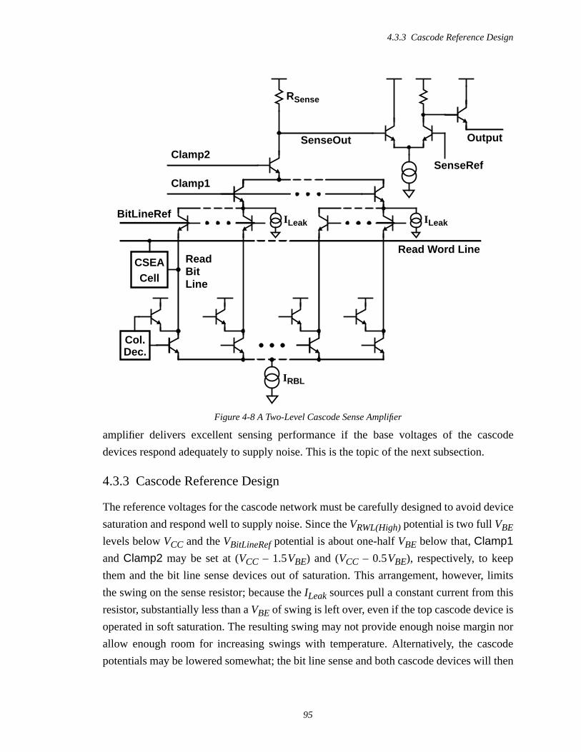
4.3.3 Cascode Reference Design
95
amplifier delivers excellent sensing performance if the base voltages of the cascode
devices respond adequately to supply noise. This is the topic of the next subsection.
4.3.3 Cascode Reference Design
The reference voltages for the cascode network must be carefully designed to avoid device
saturation and respond well to supply noise. Since theVRWL(High) potential is two fullVBE
levels belowVCC and theVBitLineRef potential is about one-halfVBE below that,Clamp1
and Clamp2 may be set at (VCC – 1.5VBE) and (VCC – 0.5VBE), respectively, to keep
them and the bit line sense devices out of saturation. This arrangement, however, limits
the swing on the sense resistor; because theILeak sources pull a constant current from this
resistor, substantially less than aVBE of swing is left over, even if the top cascode device is
operated in soft saturation. The resulting swing may not provide enough noise margin nor
allow enough room for increasing swings with temperature. Alternatively, the cascode
potentials may be lowered somewhat; the bit line sense and both cascode devices will then
IRBL
RSense
CSEACell
SenseOut
ILeak ILeak
SenseRef
Output
Clamp2
Clamp1
BitLineRef
Read Word LineReadBitLine
Col.Dec.
Figure 4-8 A Two-Level Cascode Sense Amplifier

4.3.3 Cascode Reference Design
96
operate in “soft” saturation (i.e. with their base-collector junctions slightly forward
biased), increasing the available swing for the sense resistor. This latter solution requires
careful worst-case design to limit the maximum base-collector biases to prevent access
time degradation from charge storage in this junction and latch-up from excess current
injected into the substrate.
Design of the cascode references must also consider electronic supply noise. With the high
current gains provided by cascode sensing, a downward bump inVEE, coupled onto the
emitters of the cascodes, could overwhelm the current being sensed. With two-level cas-
code sensing, the major source of noise currents are the first-level cascodes that have only
unselected bit lines, since there are many more unselected cascodes and thus more poten-
tial noise current sources. Reducing the percentage coupling toVEE of the sensitive nodes
is clearly desirable, but only the wire capacitances (which may be routed overVCC-con-
nected material rather than theVEE-connected substrate) may be coupled toVCC without
penalty; this is sufficient for the second-level cascode device, whose emitter capacitance is
largely wire. ExplicitVCC capacitance may be added to the emitter nodes of the first-level
cascodes, but is undesirable because it slows the sensing speed. Simulations indicate that
making the first-level cascode’s base (i.e.Clamp1) coarsely track the voltage response of
an “unselected” first-level cascode’s emitter (via a replica network) greatly improves the
noise response.
If Clamp1 exactly tracked the emitter response of unselected first-level cascode transis-
tors, then theirVBE would not change so they would pull no noise current from the sec-
ond-level cascode device. The reference generator of Figure 4-9 makesClamp1 nearly
match the behavior of unselected cascode emitters. The circuit employs a replica first-
level cascode circuit, with diode-connected BJTs in place of the cascode stack. Although
the current through the pull-up resistor changes as the replica emitter node,
CascodeMatch, responds to supply noise, the current difference is small enough that the
response is not greatly altered. BecauseILeak is small, it is poorly suited for directly driv-
ing the generator output, so emitter followerQ1 buffers the replica emitter value, which is
then level-shifted up to drive the output. SinceClamp1 is generated by bothVBE andIR
drops, it is simple to makeClamp1 track level and swing variations with temperature.
This reference generator keeps the two-level cascode sense amplifier largely insensitive to
supply noise.

4.3.4 Results
97
4.3.4 Results
In order to assess the performance offered by the techniques described thus far this chap-
ter, a circuit model for the sense path of a 64K×4 CSEA memory is simulated to deter-
mine its access time under transient supply variation. The stimulus is a diode decoder with
switched PMOS load, which drives a Darlington word line driver and delivers a 550-mV
read word line swing, as determined in Section 4.2.3. In order to simulate the effects of
random supply noise, a±300-mV/nsVEE voltage pulse is moved in time relative to the
stimulus to determine the position in which the noise most delays the access.
Figure 4-10 shows the worst-case access, where a –300-mV/nsVEE noise pulse start 0.1ns
before the word lines cross. The figure depicts a transition from reading a cell storing zero
to a cell storing one. From the figure, the effects of the noise pulse are clearly evident in
the sensed data value (SenseOut) and the sense amplifier reference (SenseRef). The
access penalty due to the noise source is only 0.25ns, which is 18% of the total delay from
the word line crossingBitLineRef to the sense amplifier outputs resolving. With such per-
formance, it is clear one may construct CSEA SRAMs that retain their speed advantages
in the face of supply noise.
A principal component of the sense delay for this bit line sense method is the time
required to charge and discharge the bit lines. Switching from reading zero to reading one
on an active bit line has the longest delay because the cell follower does not turn on until
the read word line rises fromVRWL(Low) to VBitLineRef. The actual delay is lengthened by
Q1
1.5IRef
ILeak
Clamp1
BitLineRef
IRef
CascodeMatch
Replica First-Level Cascode Load
Figure 4-9Clamp1 Reference Generator

4.4 Pulsed Sensing
98
theRC time constant that results from the resistance ofP1 and the effective base capaci-
tance ofQ1. This path is slower than the one-zero transition by approximately 0.3ns. The
next section introduces a new sensing method that reduces this delay by beginning each
access with the word line level equal to the bit line reference, which minimizes the bit line
voltage change required to resolve the access and thus improves the delay.
4.4 Pulsed Sensing
Chapter 3 describes the use of pulsed circuit techniques to reduce the delay and power dis-
sipation of low-swing decoders. This section applies the pulsed current sources and
switched PMOS loads of Chapter 3 to the sense path of a CSEA memory, thereby deliver-
ing similar performance gains. As in the decoders, the ability to begin each access in a
known state (and thus tailor the selection and reset waveforms on each node) provides the
basis for delay reduction. In particular, by resetting the bit line to a lower voltage and then
pulsing both the word line and the bit line reference, the sensed current resolves more
quickly than in the sensing method of Section 4.3.
2.5
3.0
3.5
4.0
4.5
5.0
5.5
6.0V
olta
ge (
V)
0.0 0.5 1.0 1.5 2.0 2.5 3.0 3.5 4.0Time (ns)
Falling Word LineRising Word LineSenseOutSenseRefData Out
Figure 4-10 Sense Path Performance with Supply Noise

4.4.1 Theory of Operation
99
Pulsed techniques also save power by only activating current sources when a signal could
transition. Such savings are especially important for wide access width memories, which
read more bits at once and therefore use more sensing power. While their power dissipa-
tion may be higher than narrow width SRAMs, wide-word memories are typically faster
because they require less column multiplexing. Because key circuit techniques of the sec-
tion require per word overhead, the control complexity and power, and the memory den-
sity, of such circuits are minimized for wide-word CSEA memories. This section opens
with a discussion of the basic pulsed bit line circuits, continues with peripheral and refer-
ence circuitry that support the bit lines, and closes with simulation results that quantify the
performance advantage of pulsed CSEA sensing.
4.4.1 Theory of Operation
With pulsed signalling the differential pair formed byQ1 and the sense device can be reset
to levels that minimize the sensing delay by reducing the voltage change both on the bit
line and on the internal cell node that is required to switch the bit line current. The simpli-
fied differential pair of Figure 4-11, switches the fastest if the input is reset to the reference
potential, becauseIRBL is steered to one side or the other as soon as the input begins to
transition. The CSEA sense situation is more complicated, due to the extra (N – 1) unse-
lected cell followers on the bit line. If all the word lines are reset toVBitLineRef, the rising
selected word line will rapidly steer the bit line current away from the sense device if the
selected cell stores one. However, when the selected cell stores zero, the unselected cells
that store one become important. In order to let the sense device steer the bit line current,
the unselected word lines must therefore fall fromVBitLineRef.
While this arrangement delivers very fast access, it is completely impractical because it
forces all of the read word lines in a bank to transition, which requires too much power. If
the access begins with all word lines andBitLineRef reset toVRWL(Low), and the selected
Q1Q2
IRBLCRBL
ISense
BitLineRefReadWordLine
Figure 4-11 Oversimplified Bit Line Sense Model
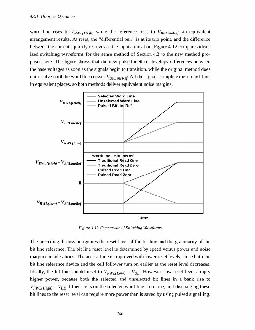
4.4.1 Theory of Operation
100
word line rises toVRWL(High) while the reference rises toVBitLineRef, an equivalent
arrangement results. At reset, the “differential pair” is at its trip point, and the difference
between the currents quickly resolves as the inputs transition. Figure 4-12 compares ideal-
ized switching waveforms for the sense method of Section 4.2 to the new method pro-
posed here. The figure shows that the new pulsed method develops differences between
the base voltages as soon as the signals begin to transition, while the original method does
not resolve until the word line crossesVBitLineRef. All the signals complete their transitions
in equivalent places, so both methods deliver equivalent noise margins.
The preceding discussion ignores the reset level of the bit line and the granularity of the
bit line reference. The bit line reset level is determined by speed versus power and noise
margin considerations. The access time is improved with lower reset levels, since both the
bit line reference device and the cell follower turn on earlier as the reset level decreases.
Ideally, the bit line should reset toVRWL(Low) – VBE. However, low reset levels imply
higher power, because both the selected and unselected bit lines in a bank rise to
VRWL(High) – VBE if their cells on the selected word line store one, and discharging these
bit lines to the reset level can require more power than is saved by using pulsed signalling.
Figure 4-12 Comparison of Switching Waveforms
WordLine - BitLineRef
VRWL(Low)
VBitLineRef
VRWL(High)
Selected Word LineUnselected Word LinePulsed BitLineRef
Time
VRWL(Low) - VBitLineRef
0
VRWL(High) - VBitLineRefTraditional Read OneTraditional Read ZeroPulsed Read OnePulsed Read Zero

4.4.2 Pulsed Bit Line Circuitry
101
Furthermore, low reset levels increase the unselected bit line sensitivity to supply noise,
since drops in supply levels could cause the bit lines to fall enough to turn on their sense
device. Another problem with low reset levels involves variation in the word line rise
times due to differences in loading between word lines connected to cells that store mostly
one or zero; cells that store one impose a higher load due to the base charge required by
the cell follower to charge its bit line. The problem with this variation is the difficulty in
building a bit line reference driver that tracks the variation.
With pulsed signalling, a hybrid solution is possible that provides fast access at reasonable
power. By resetting the bit lines near the active zero level (i.e.VBitLineRef – VBE), the
swing on unselected bit lines that store one and the word line loading variation are reduced
to manageable levels. Furthermore, the access delay may be reduced by activating a
pulsed bit line current source and releasing the reset circuitry at the same time the word
line and bit line reference are rising. Because the internal cell voltage lags the word line
level due to the current required to charge the cell follower, there is enough time to par-
tially discharge the bit line before the cell follower turns on. In this way selected bit lines
effectively have a lower reset level, which improves their speed.
With a reset level at approximately the active zero level, unselected bit lines in the
selected bank can couple noise into the sense network if their bit line reference rises
enough to turn on the sense device. For this reason, the bit line reference must be driven
on a per-word basis, so only selected bit lines ever have a rising bit line reference.
4.4.2 Pulsed Bit Line Circuitry
A circuit diagram of such a pulsed bit line appears as Figure 4-13. The bit line circuitry is
somewhat similar to the static case, with a NMOS reset device (N1) replacing the bit line
pull up device and with a pulsed current source replacing the steered bit line current. In the
reset state, all of the read word lines, the bit line reference, and the pulsed current source
control (BitLineCS) are low, while the bit line reset,BitLineReset, is high soN1 sets the
bit line to its reset levelBitLineResetRef.
As an access begins,N1 must turn off so that it does not interfere with the access. While
the row decoder raises the selected word line, the column (i.e. word) decoder in each bank
activates the pulsed current sources and the bit line reference for the selected word. The
selected bit lines therefore begin to drop until they are met by either the rising word line (if
their selected cells store one) orBitLineRef; in either case the bit lines begin rising, and
the capacitance of the bit lines provides additional loading, and hence additional sense

4.4.2 Pulsed Bit Line Circuitry
102
current that is steered throughQ1 or Q2. While the bit lines rise this excess current helps
the sense network resolve its answer more quickly, and allows the size of the pulsed cur-
rent source to be reduced. Once the sensed current resolves, the sense amplifier must latch
the result before the pulsed bit line current turns off, or else the data will be lost.
At the end of the access all of the control signals return to their reset levels, so
BitLineReset turnsN1 back on to reset the bit lines. The sense path thus prepares for its
next access. Simulated waveforms for a single access appear as Figure 4-14. The wave-
forms include two bit lines from the selected word: one that stores zero and one that stores
one.
TheBitLineReset signal deserves special mention. Because the reset level of the bit line
is aboutVCC – 3.5VBE, BitLineReset only needs to drop this low to turn offN1 during an
access. This lets theBitLineReset driver be implemented from bipolar logic, since the
low level does not saturate the current source. A swing of about 2.5VBE is enough onN1,
which only needs to turn on hard enough to reset the bit lines. As the figure shows, the
BitLineReset driver overshoots its DC level, which reducesN1’s resistance and thus
speeds the bit line reset. A secondBitLineReset issue involves the unselected bit lines of
Q1
Q2
BitLine
BitLineRef (per word)
Selected Word Line
N1
PulsedBit LineCurrentCSRef
VSS
BitLineReset (per bank)
BitLineResetRef
BitLineSel (per word)
SenseOut
Figure 4-13 A Pulsed CSEA Bit Line

4.4.3 Peripheral and Reference Circuits
103
the selected bank. Since these bit lines will be pulled up by any selected memory cells that
store one, the reset circuitry should not fight these transitions. For this reason,
BitLineReset should be shared by all the words in a bank, so all bit lines in that bank are
released when any word is accessed.
The cascode sense amplifier is nearly identical to the static sense amplifier of Section 4.3.
In particular, a single-level cascode network is usually sufficient for wide word accesses,
which require less column multiplexing. For instance, a memory with a 64-bit word
requires sixteen times less column multiplexing that a 4-bit access, so the number of col-
lectors on the cascode node of a wide memory is no more that the number of collectors on
the (global) second-level cascode node of the narrow memory.
4.4.3 Peripheral and Reference Circuits
The performance advantages of pulsed sensing are obtained only if peripheral circuits
generate well-timed signals at desired potentials. This subsection describes circuits to
2.0
2.5
3.0
3.5V
olta
ge (
V)
ReadWordLineBitLineRefBitLineSel
BitLineResetRefBitLine0BitLine1
1.0 2.0 3.0 4.0Time (ns)
1.0
2.0
3.0
4.0
5.0
Vol
tage
(V
) BitLineReset
Figure 4-14 Simulated Pulsed Bit Line Waveforms

4.4.3 Peripheral and Reference Circuits
104
generate theBitLineRef, BitLineCS, and BitLineReset signals, as well as the
BitLineResetRef reference.
In order to achieve fast sensing with adequate noise margins,BitLineRef must track the
characteristics of a typical word line, albeit at a lower swing. To accomplish this, one
could build the reference driver using the same circuitry as a word line, with a resistive
voltage divider between the dummy word line level and the low word line level to accom-
plish the amplitude reduction. Unfortunately, the resistive divider alters the characteristics
of the resultingBitLineRef: if the resistors are large then there is delay in the rising wave-
form that delays the access, and if the resistance is reduced then the current through the
resistors alters the shape of the dummy word line swing, which ruins its tracking.
Alternatively, theBitLineRef driver of Figure 4-15 utilizes a dummy word line (with all
cells storing zero) and the same basicNOR gate and discharge circuitry as in the word line
decoder and driver, with one exception: since not all of the inputs will be needed to select
the desired word from the row, the bank current source selection signalBankSelQ may be
used to dynamically pull a fraction of the decoder current from the gate load even when
the gate is selected, thus constraining the high level of theBitLineRef signal. Because the
switched PMOS load is nonlinear, the output swing ratio of theBitLineRef driver to a
word line driver is not simply the current ratio. Furthermore, the low current density in
unselected (low) word line drivers requires that the gate output rise before the Darlington
devices turn on enough to charge their loads; this rise is subtracted from the output swings
of both a word line driver and theBitLineRef driver. Therefore, detailed circuit simula-
tions must be performed to select the proper fraction of the decoder current to switch in
when theBitLineRef driver is active; for the 0.8-µm technology describe in this thesis,
40% gives both fast access and good noise margin over process and temperature varia-
tions. Since this scheme requires one dummy word line (for loading) for each word in a
row, the area penalty is smallest for wide word widths.
The BitLineCS driver may be constructed from another pulsedNOR gate to ensure its
time correlation with the other active signals. As shown in Figure 4-16, the output uses a
simpleL3 driver from Section 3.5. The extra output is used to generate a wired-or signal
that controls per bank pulsed current sources, such as that on theBitLineReset driver and
on the sense amplifier latch.
TheBitLineReset driver is very simple; since it operates on a per bank basis and is high
in the reset state all that is required is a simple resistive load and aBankSelQ-pulsed

4.4.3 Peripheral and Reference Circuits
105
IDec
VSS
VCC
CSRef
BankSelQ
In0
BankSelP
BitLineRefRLeak
.4IDec
PulsedDischargeIn1
Figure 4-15 Pulsed Bit Line Reference
VSS
VCC
CSRef
BankSelQ
In0
BankSelP
RLeak
In1
BitLineSel
(L3)
Wire-Or
CSRef
BankSelQ
BitLineReset
Figure 4-16 Pulsed Bit Line Control Circuits

4.4.3 Peripheral and Reference Circuits
106
current source, with a pulsed emitter follower output. The output current is controlled by
theOR of theBitLineCS signals for the bank so that theBitLineReset signal has similar
timing. With a 2.5-VBE swing on the resistor theBitLineReset level isVCC – 3.5VBE,
which is enough to turn off the reset devices. The delay associated with discharging
BitLineReset is not critical because the current available from the reset devices is sub-
stantially smaller than the pulsed bit line current, so the delay does not increase much if
BitLineReset is a little late.
The desired bit line reset value is defined relative toVCC, since it involves signals gener-
ated from that supply, but with an on-chipVSS generator the difference between the reset
value andVSS is well specified, so the reset references may be defined relative to which-
ever supply makes the design simpler. Because the predominate dynamic current required
to reset the bit lines comes from discharging unselected bit lines where the selected cell
stores one,BitLineResetRef must be able to supply large discharge currents and it is
therefore convenient to giveBitLineResetRef a diode-like characteristic; as Figure 4-17
shows, this is readily accomplished using aVBE multiplier circuit to build a programmable
diode of the desire value.
Q2 supplies leakage current to prevent inactive bit lines from drooping and the current
required to keep theVBE multiplier looking like a diode; it does not need much active cur-
rent because the operation of the bit line prevents it from ending an access much below
BitLineResetRef. Since it’s primary output is a current whose value should be controlled
to limit the inactive bit line currents,Q2’s base is generated using the simple current
1 1
Q2
10012I
VSS
VCC
Q1
~I
~I
BitLineResetRef
VBEMultiplier
Figure 4-17 Pulsed Bit Line Reset Reference

4.4.4 Results
107
mirror-based feedback circuit shown in the figure. To minimize the power dissipation, the
reference divides the follower current by 100; the static current source supplies twice this
current to compensate for the base current of the follower. The large capacitance slows
down the voltage response of the base to current spikes, since the output voltage should be
based on long-term average currents. Note that the resulting base potential is determined
entirely by the leakage current required by the bit lines and the static current inQ1, so
BitLineResetRef is truly determined by theVBE multiplier.
The sense amplifier reference may be constructed as in Section 4.3.1, with two reference
columns (one mimicking reading one and the other zero) per word. Simulations indicate
that the reference behavior more closely tracks the worst-case bit lines when the data val-
ues on the reference lines are interleaved (i.e. each reference line stores half ones and half
zeroes, but the two lines always store opposite values on any give word line).
4.4.4 Results
A simulation model of one bank in such a pulsed bit line CSEA SRAM was constructed to
estimate its performance. With 64-bit words, 256 cells per word line, and 64 cells per bit
line (i.e. the same bank parameters as in the previous section) plus four dummy word lines
per bank for the pulse bit line reference circuits, the sensed bit line currents cross their ref-
erence values about 1.0ns after the decoder inputs transition. The slowest read access is
reading zero from a bit line that stores ones in all other cells (due to increased base-emitter
capacitance) on a word line where all other cells store one (since ones require charging the
cell follower’s base-emitter junction). This access is depicted in Figure 4-14. The current
through the bit line sense device crosses that of the replica bit line’s reference only 0.35ns
after the selected word line reaches midway, which is much less than the 0.85-ns delay for
the original static bit line sensing technique.
The pulsed sense path is more robust than the static path with respect to supply noise.
While the static bit line current is reduced by roughly half, the pulsed bit line reference and
word line signals deliver dynamic sensed currents during the signal transitions that nearly
equal the static bit line current of Section 4.3. Since the currents are nearly equal when the
signals are most vulnerable to supply noise, the delay caused by a certain amount of supply
noise is similar. However, the on-chipVSS generator, which makes effective use of the
decoupling capacitance of the memory arrays, limits the maximumVSS edge rates to
roughly one quarter of the 300mV/ns rates simulated in the previous section. Thus, the
pulsed path has nearly the same sensitivity to supply noise, but less noise to deal with.

4.5 CSEA Writing Techniques
108
Pulsed decoding and sensing are able to substantially reduce the access time of a CSEA
SRAM. However, the performance of a CSEA memory can be limited by the delay in its
write path. The next section focuses on ensuring that memory writes do not limit the
achievable cycle time.
4.5 CSEA Writing Techniques
The read port of the CSEA memory cell permits the construction of very fast SRAMs with
only low-swing signals in the read access path. However, the write port requires large
swings on its write word line and write bit line in order to successfully overpower the
CMOS latch that forms the storage element. Thus, some sort of level conversion is
required. A low-power word line level converter suitable for this purpose is discussed in
Section 3.6. Similar converters may be readily constructed to provide large-swing bit line
signals as well.
The principal other challenge is to rapidly write the CSEA cell through its single access
device while not writing unselected cells on the selected write word line. The next section
discusses this issue in more detail, while Section 4.5.2 proposes an effective way to deal
with the challenge by avoiding partial write selection altogether.
4.5.1 Single-ended Versus Differential Cell Writing Issues
The traditional 6T CMOS memory cell of Section 2.2.1 is written through two NMOS
access devices, each of which is connected to one of the differential bit lines. In order to
write the cell, the access transistor on the side of the cell that needs to drop overpowers the
PMOS pull-up device, discharging the internal cell node until reaching the switching point
of the other inverter in the cell. Once the switching point is reached, the positive feedback
of the cell storage latch completes the change in state. To accomplish this, the bit line on
the discharging side of the cell is driven low to provide the discharge current, while the
other bit line is held at a relatively high level to minimize any effects from this opposing
bit line. Because the write access width is typically smaller than the number of cells on
each word line, there are usually cells on the selected word line that should not be written.
Avoiding suchwrite disturbance for the 6T cell simply requires keeping both cell bit lines
at a high enough value that they cannot supply enough current to flip the cell; because
these bit lines are used for both writing and reading the cell, the starting value for reading
is chosen to be this “safe” level so that inactive bit lines do not need to transition between
read and write accesses.

4.5.1 Single-ended Versus Differential Cell Writing Issues
109
The CSEA memory cell (see Figure 4-1) has only one write access deviceN3 and thus its
write bit line typically must perform three functions:
• Writing one — SinceN3 is connected to the complemented side of the cell, a cell
value of one implies a low voltage at the access device so to write one the bit line
must be low enough for the access device to overpower the weaker PMOS pull-
up transistorP2.
• Writing zero — In a similar way, writing zero requires that the access device over-
power the NMOS pull-down deviceN2, so the bit line must be high.
• Avoiding write disturbance — For unselected cells on the selected word line, the
bit line must be high enough not to overpowerP2, and low enough not to over-
powerN2.
The width ofN3 should be larger thanN2 so that there is adequate noise margin in writing
zero, especially since NMOS transistors pull down better than up; this makes it much eas-
ier to write one, thus raising the bit line voltages at which ones may be written. Unfortu-
nately, this reduces the voltage range where writes will not occur, increasing concerns
about write disturbance. By reducing the switching point of theN1-P1 inverter, the width
of N3 may be reduced since writing zero becomes simpler.
In his thesis, Yang [49] discusses these issues in great detail and describes a method to size
all of the cell transistors to provide both robust writes and minimal disturbance to unse-
lected cells. However, the resulting transistor sizes are mostly non-minimum, and there-
fore the CSEA cell area increases. Furthermore, while the resulting static noise margins
are large enough to be safe, they are not so large that writes occur very quickly. In other
words,N3 is not large enough that its current easily overpowers that ofN2, so writing
zero takes much longer than on a 6T cell. Finally, driving three-level write bit lines is dif-
ficult, so the bit line control circuits tend to require more delay than those for differential
writes.
An alternative would be to add an additional NMOS device to the CSEA cell, which
would allow differential writing. This solution, however, increases cell area, primarily by
requiring an extra write bit line that must contact each cell. Because memory density is a
critical component of overall SRAM performance, there is room only for a single write bit
line in a high-performance CSEA design.

4.5.2 Local Word Line Qualification
110
4.5.2 Local Word Line Qualification
The performance issues associated with three-level CSEA write bit lines, namely cell den-
sity and write time penalties, are so severe that one should consider the system-level envi-
ronment to provide a workable solution. Since most RAMs (and certainly all on-board
caches for microprocessors) access multiple bits at a time, the write disturbance problem
may be avoided entirely by doing a full X-Y select on the addressed word; if the unse-
lected words on the selected row do not have a high write word line, the bit lines require
only two levels.
A simple circuit to perform this write qualification is shown in Figure 4-18. It is essen-
tially identical to the local word line driver used in many CMOS SRAMs that employ
divided word line techniques [14] (see Section 2.2.3). Note that the global write word line
is active low, but neither the extra gate that drives the global word line nor the qualifica-
tion gate should add much delay since the existing buffer stages are already heavily
loaded, and therefore proper buffer tapering absorbs the delay. The other input to this cir-
cuit is a full-swing column select signal, which is produced much like the write word line.
The circuit consists of anAND gate that looks like a CMOS inverter with the global word
line as its input and the column select line as its positive supply. The loading of these gates
on the column select line is comparable to the loading of the write bit lines, which are also
driven by the column decoder, so the delay times should be similar.
CSEA
Cell
ColumnWriteSelect
WriteBit
Line
ReadBit
Line
WriteWordSelect
ReadWordLine
LocalWriteWordLine
Global WriteWord Line
(active low)
Figure 4-18 Write Qualification Circuit

4.6 Summary
111
Since each such gate drives multiple cells (i.e. the access width), the area penalty of the
local word line drivers is amortized across the access width; for a 4-bit wide CSEA design
the cell array area increased only 16% to accommodate the drivers (see Section 5.1). The
area penalty drops substantially for larger widths, since the area penalty for splitting the
memory array is much larger than the penalty for increased driver width as the word width
grows. The addition of the global write word line does not increase the cell area, since it
replaces the metal wire that would run over the higher resistivity polysilicon word line to
improve theRC word line delay in a conventional design.
The overall write performance of such a design is quite good. With local word line qualifi-
cation, write disturbance ceases to be an issue, so the cell may use minimum-sized devices
for N1, N2, andP2; P1 is typically larger to reduce the effective base resistance ofQ1
and thereby reduce the base-charging delay.N3 should be large enough to easily over-
powerN2, and thus quickly flip the cell. Thus, word line qualification permits the use of
dense CSEA cells that write quickly, at very modest area penalty and without the use of
fancy three-level bit line drivers.
Furthermore, the use of the low-power level converter further improves write perfor-
mance. By adopting similar level converters for the write word line, column select, and
write bit line paths, all the signals that accomplish a write have similar delays. With nearly
equal delays and active times, the write path can accomplishwave pipelined writes, where
the current write need not finish before the next read or write cycle may begin. This is pos-
sible because of the independent read and write ports of the CSEA memory cell. With this
capability, the delay requirements of the write path may be somewhat relaxed, since the
overall SRAM may then have a cycle time that is shorter than the actual write path delay.
The word line level converter and the local word line qualification circuit thus prevent
write delays from limiting the cycle time of CSEA memories.
4.6 Summary
Sensitivity of the single-ended read bit line of the CSEA memory cell to electronic supply
noise has been considered a significant barrier to the construction of robust CSEA
SRAMs. This chapter shows that electronic supply noise need not limit the performance of
such memories. It describes techniques that can robustly sense and amplify the data stored
within a CSEA cell with very low delay. Because of the high read current of a CSEA cell,
the bit lines are fairly tolerant of capacitive coupling from the power supplies. The

4.6 Summary
112
two-level cascode sense amplifier and replica bit line circuits of Section 4.3 provide quick
access for large CSEA memories while maintaining good noise immunity. Section 4.4
describes the application of pulsed circuit techniques to the sense path, and the perfor-
mance gains that may be obtained.
This chapter also discusses issues associated with the write path of CSEA memories. The
problems with single-ended writing, namely fancy three-level write bit lines, skewed cell
device ratios that decrease memory density, and slow write times, which all arise from
avoiding write disturbance, are described and then eliminated. Using a simple word line
qualification gate borrowed from divided word line memories, only the cells to be written
are connected to an active write word line, thus removing concerns about disturbing unse-
lected cells on the selected word line.
In combination with the decoding techniques of Chapter 3, the sense and write techniques
of this chapter enable the construction of very high performance CSEA memories. The
next chapter explains the results of applying these circuit techniques to high-density, high-
speed, and reasonable power CSEA SRAMs.

Chapter 5 Results
113
Chapter 5
Results
This thesis has presented a number of new circuit ideas to improve the performance of
various SRAM building blocks. This chapter describes the results of combining these
building blocks to construct CSEA-based SRAM subsystems. The three designs of this
chapter illustrate the system-level performance advantages of the techniques of this thesis.
The designs differ from one another in two important ways. First, the described SRAMs
each have a different target. The first one is a research prototype, built to demonstrate the
feasibility of some core circuits and verify a memory cell design. The second design is a
standard asynchronous SRAM with substantially more design effort invested in process,
temperature, and supply variation considerations and is a more appropriate match for the
technology in terms of die size, memory capacity, access time, and power dissipation. The
third design is a synchronous SRAM subsystem that utilizes the new pulsed ECL circuit
ideas of Chapters 3 and 4 to provide greatly-improved access times. The other major dif-
ference between the designs is the level of design experience. The designs are presented in
chronological order, so the successive designs show an increasing level of design maturity.
All of the designs utilize the 0.8-µm BiCMOS technology discussed in Chapter 1 and used
in examples throughout this thesis. Furthermore, all designs share the same basic cell lay-
out and array sizing, which makes comparisons among the designs simpler. The CSEA
cell occupies 154µm2, although Section 5.1.1 describes how the same cell could be built
in only 125µm2. The banks each contain 64 rows and 256 columns of memory cells,
although some designs add extra cells to generate the sense amplifier reference. The input
and output buffers, as well as the row decoder, word line driver, column decoder, sense
circuitry, and write circuitry vary between designs.
This chapter begins with a discussion of an experimental 16K×4 SRAM that was fabri-
cated in 1989. The next section discusses improvements to the basic design required to
produce a higher performance and more robust 64K×4 SRAM. Section 5.3 describes a

5.1 An Experimental 64K CSEA SRAM
114
prototype on-chip synchronous SRAM subsystem that delivers significantly faster access
and cycle times at nearly identical power dissipation.
5.1 An Experimental 64K CSEA SRAM
Some of the early circuit ideas from this thesis were successfully integrated in a 64-Kb
CSEA SRAM that was fabricated in 1989. The fabricated die has two significant layout
errors that required post-fabrication modification, as described in Section 5.1.3. Further-
more, the limited available die area forced the design away from its performance target.
With decoding circuits that deliver greater power savings as the number of banks
increases, the power performance of a 64-Kb design with a relatively small number of
banks (since the bank design was optimized for a 256-Kb SRAM) is worse than could be
achieved. However, this SRAM does deliver impressive performance, and it provides both
measured results and extracted design database information that are crucial for the design
of the later SRAMs. This section begins with a description of the cell design, discusses the
chip architecture, and shows the circuits used in the design. It next describes the test and
measurement results, and closes with a description of what key knowledge was gained in
the implementation.
5.1.1 Cell Design
The basic CSEA memory cell schematic, reprinted in Figure 5-1, provides the starting
point for the cell design, which has two interrelated parts: device sizing and physical lay-
out. The two parts are related by the restrictions that layout design rules place on the
device sizes and by the effects of layout parasitics on the cell performance. For ease in
generating design rule-correct layout, all physical layout of the chip was constrained to fit
on a 0.4-µm grid, so device sizes were limited to multiples of 0.4µm.
The device sizing process began with all minimum devices to minimize total cell area; for
MOSFETs the minimum gateW/L was 1.2µm/0.8µm, while a minimum bipolar device
had a 1.6-µm×0.8-µm emitter area. Device sizes were then increased for three different
reasons:
• P1 grew to reduce its on resistance and thereby reduce the base charging delay
for Q1, which is an important component of the sensing delay.
• N3 grew to make sure it was strong enough to overpowerN2 and thus write zero
into the cell. Since the SRAM uses local write qualification, write disturbance is

5.1.2 Organization
115
not an issue so there are no constraints other than cell area and bit line capacitance
that limit the maximumW of N3.
• N1 andP2 grew to adjust the switching point of theN1-P1 andN2-P2 inverters
to make it easier to write the cell; this requires less area than simply increasingN3
further due to the extreme aspect ratio of the cell layout.
Figure 5-1 shows the final device widths in microns.
The resulting cell layout is show in Figure 5-2. A key feature of the fabrication technology
that permits a small cell layout is the TiN “local interconnect”, which provides a contact
between the gate polysilicon and the drain diffusion without requiring any contact to the
metal layer. The cell area is further reduced by not including a collector contact in each
cell, by merging the collector and n-well regions, and by merging the base region ofQ1
with the source ofP1, as is discussed in Section 4.1. The cell measures 154µm2, but this
relatively large area is partly due to the design grid. The same device sizes may be inte-
grated in only 125µm2 if the design grid is relaxed to 0.1µm. This cell size compares quite
favorably to the 117-µm2 256-Kb 6T CMOS cell, built in the same technology, which is
reported in [25], especially since the CSEA cell delivers twice the read current of that 6T
design.
5.1.2 Organization
The memory is organized as 16K words by 4 bits; internally the SRAM is divided into
four (4K×4) banks, each with 64 rows and 256 columns. The local write qualification
gates and collector contacts occur every eight cells, since two qualification gates share a
vertical track and drive opposite local write word lines; with such an arrangement no
Figure 5-1 Fabricated CSEA Memory Cell
P2 (1.6) P1 (2.8)
N2 (1.2) N1 (1.6)
Q1
N3 (2.0)
Read Word Line
Write Word Line
ReadBitLine
WriteBit
Line

5.1.2 Organization
116
bipolar transistor is more than four cells (about 30µm) away from a collector contact, and
with the buried layer under the collector and n-well regions the extra series collector resis-
tance is less than 100Ω.
A block diagram of the chip appears as Figure 5-3. The row decoders and word line driv-
ers are placed in the center of each memory bank to reduce theRC delay of the read word
line. The chip contains 4 sets of row decoders, but only two sets of column decoders
because vertically adjacent banks share the same decoders. While the independent row
decoders ensure that only one read word line is selected at any time, the shared column
decoders switch currents into four selected read bit lines both above and below the
decoder. The bit line reference devices and two-level cascoded sense amplifiers (see
Section 4.3) are on the opposite end of the bit line from the decoders, so there are parallel
6.8 x 22.6 microns
Bit LinesWriteRead
Emitter
N Diffusion
P Diffusion
Base
N-Well / Collector
Local
Polysilicon
Contact
Metal 1
Via
Metal 2
Local Write Word Line
Global Write Word Line
Vss
Read Word Line
Figure 5-2 CSEA Cell Layout

5.1.2 Organization
117
sensing paths on the top and bottom of the chip, which are multiplexed at the output
buffer. The address buffers and switched PMOS resistor selection drivers, as well as the
on-chip reference generators, are near the center of the die to minimize the propagation
delay of their signals to the decoders. Input write data and write enable signals enter the
chip from the left side and are converted to CMOS levels, while the read data output buff-
ers are at the right side; all data and address I/O occur using ECL 10K-style levels.
Both decoding paths utilize the same basic circuitry; pre-decoding address buffers drive
diode decoders with switched PMOS load resistors. The pull-down current for both row
and column decoders is switched between separate address line sets for the left and right
sides; thus, the two banks of row decoders on each side share address lines. The read word
line drivers are simple Darlington pairs with resistively-coupled shared static current dis-
charge, while the write word line driver uses the read word line value to convert to CMOS
swings and drive an active-low global write word line across the array to the local word
line qualification gates. The bit line drivers steer shared currents into eight read bit lines,
while releasing the reference devices that hold those bit lines high enough to prevent inac-
tive bit lines from injecting current into the sense network. On writes the bit drivers also
Figure 5-3 16K×4 SRAM Organization
RowDec
Memory Array
Row and Bank
RowDec
Memory Array
ColumnPre-DecAddressBuffers
Column Decode & WriteWriteDataXvrt
Out-PutBuf
Two-Level Sense AmpTwo-Level Sense Amp
Two-Level Sense AmpTwo-Level Sense Amp
Addresses
ColumnAddresses
InputData
OutputData
RowPre-Dec
Buffers &Bank Sel
Address
RowDec
Memory Array
RowDec
Memory Array
Column Decode & Write

5.1.3 Measured Results
118
send the converted input data onto the write bit lines while raising the column select input
to the write qualification gates.
Thecritical (i.e. slowest) access path through the read circuitry begins with a transition of
the most significant address bit, which selects between the left and right half of the mem-
ory. As shown in Figure 5-4, this address pin drives an ECL inverter that controls the dis-
charge current for the switched resistor selection signal (BankSelP). This path has the
largest delay because no other path needs two current switching stages to get to the decod-
ers. Furthermore, the critical path passes through the row decoders because the word lines
have more delay than the bit lines. Another path from the same address input drives a pre-
decoding address buffer to generate theBankSelQ signal; this path is faster because it
requires only a single current switch delay.
5.1.3 Measured Results
A chip photomicrograph of the fabricated 16K×4 memory appears as Figure 5-5; the fig-
ure is rotated 90° relative to Figure 5-3 to better fit the page. The die measures
6.0×4.4mm, although the active die including all routing occupies less than 5.4×4.0mm.
Of this 21.6-mm2 active area, 54% is covered by the memory cells and write qualification
gates; the qualification gates add 16% to the array areas, including the area of the shared
collector contacts that would be required even without the gates. The chip is packaged in a
48-pin ceramic DIP. While this is certainly not a high-speed package, it simplifies test
board construction and provides access to internal reference signals for monitoring and
overpowering.
The fabricated chip contains two design flaws that required both laser and focused ion
beam repair. The first flaw, which results in the current source reference generator regulat-
ing at substantially higher current than desired is repaired by laser cutting a first metal
wire that links two devices in the generator; once this link is cut, the desired voltage can be
supplied from off-chip. The second flaw involves the selection signal for the output buffer
multiplexers. The chip incorrectly selects for output the data from the top sense amplifiers
when the selected word line is in a bottom array, and vice-versa. This error is repaired by
cutting the differential selection signal and re-routing it using both the sputtering and dep-
osition features of a focused-ion beam machine.
Due to problems with the write enable circuitry, the memory functions most reliably with
VCC – VEE = 5.5V; at this supply voltage the chip draws 320mA for a total power dissipa-
tion of 1.75W. At a case temperature of 70°C, the measured access time for a worst-case

5.1.3 Measured Results
119
address transition, which switches between left and right banks, is 3.7ns. An oscillograph
of such a transition appears as Figure 5-6, with the output pin driving a 50-Ω termination
to VCC – 2V. Limitations in test equipment prevent accurate measurement of the write
pulse width and cycle times, but the memory writes reliably with pulses shorter than 4ns.
Figure 5-4 Critical Access Path for 16K×4 SRAM
Left/ RightBank
AddressBankSelP
BankSelQ
ReadWordLine
BitLineRef
OutputData
Sense
Top
Data
ReadBit Line

Figure 5-5 Chip Photomicrograph of 16K×4 CSEA SRAM

5.2 Proposed 256K CSEA SRAM
121
The measured results agree quite well with circuit simulation of the extracted chip layout
plus measured package parasitics. Simulated transient waveforms for critical nodes during
a worst-case access appear as Figure 5-7. The fabricated design provided invaluable feed-
back by proving the operation of the switched PMOS load decoders, the two-level cascode
sense amplifier, and the word line level converter. The design database from the 16K×4
memory is also the starting point for the other designs, which use the same basic memory
array but change the peripheral circuits to achieve higher performance.
5.2 Proposed 256K CSEA SRAM
This section describes a 256K CSEA memory that extends the 64K design in straightfor-
ward ways. Except as noted below, the decoders and arrays are identical to the fabricated
design. A principal improvement is superior supply noise rejection provided by the sense
and cascode reference circuits of Section 4.3. The original 16K×4 memory uses reference
generators that do not track the supply sensitivities of the circuits that they control. The
access time is reduced by several means. First, the critical path is shortened by controlling
the BankSelP discharge current switch with an emitter follower-buffered version of the
0.0 1.0 2.0 3.0 4.0 5.0 6.0 7.0 8.0Time (ns)
-2.0
-1.5
-1.0
-0.5
0.0
0.5
1.0
1.5
2.0
Vol
tage
(V
)
Bank AddressData Output
Figure 5-6 Oscillograph of Bank-switching Read Access

5.2 Proposed 256K CSEA SRAM
122
input address, rather than the inverter-buffered version used above; circuit simulations
indicate an access time improvement of about 300ps. Because of increased design matu-
rity, the 256K memory has improved power partitioning to speed accesses. It also specifies
a two-level metal version of the process technology, which improves the parasitic bit line
wire resistance because the second metal layer in a two-level process is typically thicker
than second metal in a three-level process. Finally, the design specifies a more appropriate
package, so less time is lost in the package traces.
However, larger memories require longer wires, so it is important to ensure that the wires
do not slow the access. To achieve this goal, the 64K×4 SRAM uses four sets of address
lines, so each set of lines goes to four row (or two column) decoders. In order to further
minimize the address line loading, the row decoders are moved to the area between arrays.
As shown in Figure 5-8, this allows a decoder to share its address wires with the decoder
in the adjacent bank. While it improves the address line switching, this organization
Bank AddressInput RefLeft BankSelQRigh BankSelQLeft BankSelPRight BankSelP
Left Word LineRight Word LineSense DataSense RefOutput DataOutput Ref
-3.0
-2.5
-2.0
-1.5
-1.0
-0.5
Vol
tage
(V
)
0.0 1.0 2.0 3.0 4.0 5.0Time (ns)
Figure 5-7 Simulated Switching Waveforms for 16K×4 SRAM

5.2.1 Results
123
increases the delay of the read word line, since the Darlington driver sees the entire word
line resistance, rather than two half branches in parallel. To avoid this four times increase
in RC delay, the proposed design splits the Darlington pair such that the final emitter fol-
lower is still in the center of each array. Because the cell layout of Figure 5-1 has room for
extra first metal tracks, the connection to complete the Darlington pair is simple.
Another place where long wires cause problems is in the two-level cascode sense network:
the RC delay in the second-level wire, which runs the length of the die, threatens to
increase the access time. This problem is reduced by splitting the wire in the middle and
replacing the second-level cascode device with a two-emitter transistor that connects to
each wire. While placing the top cascode device in the middle of the wire increases the
distance to the output pads versus the original arrangement, this path is lightly loaded and
driven by an emitter follower, so it remains quick.
5.2.1 Results
Figure 5-9 shows a circuit simulation of a worst-case bank-switching read access for the
64K×4 CSEA design; a –300-mV/nsVEE noise pulse is placed 1.35ns after the input
Column Decode
Row
Dec.Memory Array
4Kx4
256
64
Column Decode
Row
Dec.Memory Array
4Kx4
Row
Dec.
Row
Dec.
Column Decode
Column Decode
Memory Array4Kx4
Memory Array4Kx4
Two-Level Cascoded Sense Amplifier
Two-Level Cascoded Sense Amplifier
AddressInputs
OutputSelect
DataOut
OutputBuffer
Pre-decodingAddress Buffers
Four 4Kx4
Memory Banks
Four 4Kx4
Memory Banks
Four 4Kx4
Memory Banks
Figure 5-8 64K×4 SRAM Organization

5.2.1 Results
124
transition so as to maximize the access penalty (note the similar drops inSenseOut and
SenseRef). This access requires 0.2ns for input pad, level shifting, and buffering, 0.65ns
for selecting and driving the gates of the PMOS resistors, 0.6ns for pulling up the decoder,
the Darlington pair, and the read word line (to the bit line reference potential), 0.85ns for
accessing the CSEA cell and reducing the reference device’s current to 50% of the bit line
current, 0.6ns for the two-level cascoded senseamp, and 0.5ns for the output buffer and
50-Ω output pad drive. This simulated design has a read access time of 3.4ns at a junction
temperature of 70°C, using 550-mV read word line swings and 2.3W of power. Thus, this
memory is four times larger than the 64K-bit memory and has a faster access time at a
very modest increase in power dissipation. The use of switched PMOS load diode decod-
ers limits the power increase, because adding decoder banks does not add much extra
power.
0.0 1.0 2.0 3.0 4.0Time (ns)
-3.0
-2.5
-2.0
-1.5
-1.0
-0.5
0.0
Vol
tage
(V
)
Bank AddressLeft BankSelPRight BankSelPLeft Word Line
Right Word LineSense DataSense RefOutput Data
Figure 5-9 Simulated Switching Waveforms for 64K×4 SRAM
5.3 A Synchronous 256K CSEA SRAM
125
5.3 A Synchronous 256K CSEA SRAM
This section investigates the use of the pulsed decoding and sensing techniques of Chap-
ters 3 and 4 to build faster CSEA memories. Limiting when signals may change allows the
circuits to begin each access in a reset state so that only active-going transitions are in the
critical path. Synchronous SRAMs are faster because these active transitions may be tuned
for high-speed operation without concern for the resetting (de-activating) transitions,
which are accomplished after the access by separate circuits. Since the resetting circuits
require power in addition to the active-path circuits, it is crucial to reduce this power con-
sumption to make ECL-style synchronous memories practical. The pulsed circuits of this
thesis provide the required power savings.
The 4K×64 memory uses the basic organization depicted in Figure 5-10. The emitter fol-
lower input buffers drive the input addresses to the center of the die, where the pulsed
address buffers of Section 3.5.3 generate true and complemented global address lines.
Separate bank select decoders (Section 3.5.4) simultaneously generate the per-bank
BankSelP andBankSelQ signals. At the quadrant level, wired-or gates withBankSelQ-
pulsed current sources drive the pre-decoded local address lines to the row and column
NOR decoders. The pulsed row decoder raises the selected read word line while the pulsed
column decoder activates the read bit line current and raises the selectedBitLineRef.
Finally, the sensed bit line current is multiplexed via a single-level cascode network to a
shared sense amplifier, where the sensed voltage is compared to a reference generated via
replica bit lines on the selected word line (as in Section 4.3.1).
This synchronous access path delivers impressive performance. The delay from theGo
signal, which activates the pulsed address buffers, to the crossing of the sensed data and
reference signals is only 1.7ns. This compares very favorably with the 2.7-ns delay for the
same stages of the asynchronous 64K×4 design above. Including the input and output
buffering, simulations indicate that the synchronous design requires less than 2.5ns, which
is an improvement of about 25% over the 3.4-ns asynchronous one.
The power dissipation of the pulsed ECL circuits of this memory increases with both the
pulse width and the frequency of the current source selection signals. Circuit simulations
indicate that a conservative pulse width for this design is 1ns. The pulsed discharge sig-
nals for the active-low global and local address lines and theBankSelP lines do not need
current to keep the signals low, so they could use shorter pulses. With approximately 1-ns
selection pulses, the current for the major blocks of the synchronous SRAM varies as

5.3 A Synchronous 256K CSEA SRAM
126
shown in Table 5-1. The static current of the chip is estimated at around 400mA. This cur-
rent is used both by traditional static current sources and the leakage currents of the pulsed
current sources. If all functional blocks were simultaneously active, the pulsed current
sources would use almost 300mA more current. However, the access path uses selection
signals that are delayed relative to one another such that not all blocks are active at once.
The average current at cycle times of 2.5 and 5ns is also displayed in the table. At 5-ns
cycles, the synchronous memory dissipates about the same amount as the asynchronous
one, while delivering significantly faster access.
Column Decode
RowDec
Memory
Array
Wire-ORPre-Dec
Bank SelDrivers
and
Memory
Array
MemoryArray
MemoryArray
AddressBuffers
andBank SelDecoder
Memory
Quadrant
Memory
Quadrant
Memory
Quadrant
Input
Addresses
L3 Bank and PMOS L2 AddressLinesResistor Select
L1 GlobalAddress
Lines
L2 DecodedBank Selectsand PMOSResistor Selects
Figure 5-10 Pulsed Address Line Routing

5.4 Summary
127
Table 5-1 4K×64 SRAM Power Variation
The preceding analysis does not include the power required to drive the data signals off
the memory chip, since SRAMs that are 64-bits wide are most useful for applications
desiring very high-bandwidth on-chip memories. The SRAM described here achieves
3.2GBytes/s memory bandwidth at a cycle time of 2.5ns while dissipating 2.7W. This per-
formance compares very well even with memories designed in more advanced CMOS and
BiCMOS process technologies. The power dissipation is much lower than the 15-W 256K
0.5-µm BiCMOS design of [5] that has an access time, neglecting the input and output
drivers, of 1.5ns. Our 0.8-µm pulsed memory (without itsIO drivers) is only about 0.5ns
slower. Both the access time and power dissipation are superior to the 3.5-W 3.8-ns 512K
pipelined CMOS memory of [13].
5.4 Summary
This chapter has shown some of the potential offered by the techniques of this thesis to
produce very fast BiCMOS SRAMs that have large capacity and reasonable power dissi-
pation. The increasing sophistication and design maturity of the techniques is illustrated
Functional
Block
Currents (mA) Average at Cycle Time
Static Peak 2.5ns 5ns
References 20 0 20 20
Input Buffers 25 0 25 25
Address Buffers 10 60 34 22
Bank Select Decoder 45 0 45 45
Switched Resistor Decoder 7 55 29 18
Quadrant Drivers 110 25 120 115
Row & Column Decoders 55 45 73 64
Word Line Discharge 60 20 68 64
Bit Line Currents 40 30 52 46
Sense Amplifiers 40 50 60 50
Totals 412 285 526 469
Power (Watts @ 5.2V) 2.1 1.5 2.7 2.4

5.4 Summary
128
by Table 5-2, which compares the three memory designs of this chapter. The table demon-
strates how the overall memory performance may be substantially improved by paying
careful attention to the peripheral circuits, which occupy little area but consume most of
the delay and power of an SRAM.
Table 5-2 SRAM Performance Comparison
Capacity 64K 256K 256K
Organization 16K x 4 64K x 4 4K x 64
Access Type StaticAsynchronous
StaticAsynchronous
PulsedSynchronous
Access Time 3.8ns Measured 3.4ns Simulated 2.5ns Simulated
Power 1.75W 2.3W 2.4W (200MHz)
Technology 0.8-µm BiCMOS 0.8-µm BiCMOS 0.8-µm BiCMOS
Cell Type CSEA CSEA CSEA
Array Organization 64 Rows x256 Columns
64 Rows x256 Columns
64 Rows x256 Columns

Chapter 6 Conclusion
129
Chapter 6
Conclusion
This thesis examines the question, “How can one effectively use BiCMOS fabrication
technologies to construct extremely-fast SRAMs that deliver high memory capacity and
reasonable power dissipation?” The simplest answer to this question is to use each transis-
tor type for the tasks they are best suited: low-swing bipolar peripheral circuits for fast
switching and full-swing CMOS memory cells for low power. However, such an answer
ignores the significant gains that can be achieved by a more integrated approach — one
that mixes transistor types within individual circuits to obtain superior performance.
Chapter 3 applies this hybrid approach to the problem of fast address decoding. While
low-swing bipolar circuits have traditionally provided the required speed, their power dis-
sipation is too high for many high-capacity memories. Replacing the resistive load ele-
ment in such circuits with a variable-resistance load built from a switched PMOS
transistor allows the circuit to go into a reduced-power standby mode without affecting the
output voltage. The chapter showed how the switched PMOS load improves the power
dissipation of decoders based on diodeAND gates. ForNOR decoders, the PMOS load
was combined with a new BiCMOS pulsed current source to produce an ECL gate that has
a low-power mode. Because both the PMOS load and the pulsed current source are con-
trolled by low-swing signals, the gates can be selectively powered up without added delay.
The pulsed gates therefore save power both by only powering up for a limited fraction of
the access cycle and by only requiring activation of one bank of decoders at once. The
pulsed current source relies on a special negative supply voltage, which is supplied by a
new VSS generator that uses the memory array capacitance to supply the varying current
requirements of the pulsed sources.
Achieving fast and robust sensing and writing of the hybrid CSEA memory cell was the
topic of Chapter 4. The low-swing read word line of the CSEA cell eases the amplification
requirements of the row decoder, but the single-ended read and write ports cause problems

6.1 Future Work
130
for rapid sensing and writing. Here also a mix of MOS and bipolar transistors provides a
high-performance solution. New pulsed sensing circuits dramatically reduce the sense
delay by effectively beginning the access with the bit line midway between its zero and
one levels. Furthermore, replica bit lines allow pseudo-differential sensing and careful
attention to noise coupling in the design of cascode references improve the sense margins.
In order to achieve rapid writes through a single NMOS access transistor, this thesis advo-
cates a local write qualification gate, based on the local word line driver from CMOS
SRAMs, which guarantees that only cells that are to be written have a selected write word
line. Without the constraint that the access device not write selected cells on unselected bit
lines, the cell transistor ratios can be relaxed to both minimize the cell area and the write
time. The large-swing write signals are generated by a new level converter that dissipates
no power when converting zero, so it may be efficiently integrated with the read word line
driver to avoid a dedicated write decoder while maintaining low power dissipation. This
same converter is very useful for rapidly discharging the pulsed word lines of Chapter 3.
Finally, Chapter 5 describes three CSEA SRAM designs that incorporate the concepts of
this thesis. A fabricated 3.8-ns 16K×4 CSEA memory is compared to two more-advanced
256Kb SRAMs in the same 0.8-µm technology. One, a 64K×4 extension of the fabricated
prototype, is estimated to access in 3.4ns. The other design is a pulsed synchronous
4K×64 memory that should achieve 2.5-ns access while dissipating about the same power
(2.4W) as the 64K×4 memory. While these results are impressive, we believe that there is
significantly more performance waiting to be discovered.
6.1 Future Work
Several significant avenues exist for continuing this work. One need is a concrete physical
validation of the pulsed decoder and sensing structures, as well as their support circuits.
An excellent option would be the fabrication of the 4K×64 design, for building and testing
the “real thing” would answer many questions about these techniques in undisputable
ways.
A substantial opportunity for research exists in trying to effectively apply the pulsed cir-
cuits to general-purpose logic challenges such as microprocessor datapath design. The
potential for significant power savings is very high, since such datapaths tend to have par-
allel functional units of which only one is active at once; thus fast low-swing circuits
could be readily used at reasonable power if the active units can be selectively powered
6.1 Future Work
131
up. A key challenge here is to handle the complex interactions between pulsed signals in
datapaths, which tend not to have as nicely matched delays between signal paths as mem-
ories. Good solutions to this problem will require careful considerations of the interactions
between microarchitectural and circuit issues to maximize the resulting system-level per-
formance.
Finally, the impact of continued device scaling on the feasibility of BiCMOS technology
should be addressed. While ECL-style BiCMOS circuits have survived the transition to
3.3-V power supplies, it is difficult to imagine useful bipolar-intensive circuits on chips
whose power supplies differ by less than twoVBE. Since it seems clear that the increasing
emphasis on very low-power systems for portable applications will force supply voltages
down more quickly than would normal device scaling considerations, it is likely that spe-
cial low-voltage process technologies will be required. BiCMOS does not have a future at
supplies below one volt. However, there will still be systems that plug into the wall and
that require higher switching speeds than the low-voltage technologies can provide.
BiCMOS technology may prove useful for these applications, due to the faster switching
speed of low-swing bipolar circuitry. Constructing new circuit families that can continue
to provide this advantage as the power supplies continue to shrink will be very challeng-
ing.


Bibliography
133
Bibliography
[1] Shimada, H., Kawashima, S., Matsumiya, M., Suzuki, N., et al. “A 10-ns 4-Mb BiCMOS TTL SRAM.” In IEEE International Solid-State CircuitsConference, pages 52–3, February 1991.
[2] Nakamura, K., Oguri, T., Atsumo, T., Takada, M., Ikemoto, A., Suzuki, H.,Nishigori, T., and Yamazaki, T. “A 6ns 4Mb ECL I/O BiCMOS SRAMwith LV-TTL mask option.” In IEEE International Solid-State CircuitsConference, pages 212–13, February 1992.
[3] Kato, H., Suzuki, A., Hamano, T., Kobayashi, T., Sato, K., Nakayama, T.,Gojohbori, H., Maeda, T., and Ochii, K. “A 9ns 4Mb BiCMOS SRAM with3.3V operation.” InIEEE International Solid-State Circuits Conference,pages 210–11, February 1992.
[4] Yamaguchi, K., Nambu, H., Kanetani, K., Idei, Y., Homma, N., Hiramoto,T., Tamba, N., Watanabe, K., Odaka, M., Ikeda, T., Ohhata, K., and
Sakurai, Y. “A 1.5-ns access time, 78-µm2 memory-cell size, 64-kb ECL-CMOS SRAM.” IEEE Journal of Solid-State Circuits, 27(2):167–74,February 1992.
[5] Tamba, N., Akimoto, K., Ohhayashi, M., Hiramoto, T., Kokubu, T.,Ohmori, S., Muraya, T., Kishimoto, A., Tsuji, S., Hayashi, H., Handa, H.,Igarashi, T., et al. “A 1.5ns 256kb BiCMOS SRAM with 11k 60ps logicgates.” InIEEE International Solid-State Circuits Conference, pages 246–7, February 1993.
[6] Yang, T.-S., Horowitz, M.A., and Wooley, B.A. “A 4-ns 4K*1-bit two-portBiCMOS SRAM.” IEEE Journal of Solid-State Circuits, 23(5):1030–40,October 1988.
[7] Havemann, R.H., Eklund, R.E., Haken, R.A., Scott, D.B., Tran, H.V., Fung,P.K., Ham, T.E., Favreau, D.P., and Virkus, R.L. “An 0.8µm 256KBiCMOS SRAM technology.” InInternational Electron Devices Meeting,pages 841–3, December 1987.
[8] Abu-Nofal, F., Avra, R., Bhabuthmal, K., Bhamidipaty, R., Blanck, G.,Charnas, A., DelVecchio, P., Grass, J., Grinberg, J., Hayes, N., Haber, G.,and Hunt, J. “A three-million-transistor microprocessor.” InIEEEInternational Solid-State Circuits Conference, pages 108–9, February 1992.
[9] Lin, H.C. “An optimized output stage for MOS integrated circuits.”IEEEJournal of Solid-State Circuits, 10(2):106–9, April 1975.
Bibliography
134
[10] Wendell, D., DeMaris, J., and Chritz, J. “A 3.5ns, 2K*9 self timed SRAM.”In VLSI Circuits Symposium, pages 49–50, June 1990.
[11] Heald, R.A. and Holst, J.C. “6ns cycle 256kb cache memory and memorymanagement unit.” InIEEE International Solid-State Circuits Conference,pages 88–9, February 1993.
[12] Towler, F., Chu, J., Houghton, R., Lane, P., Chappell, B.A., Chappell, T.I.,and Schuster, S.E. “A 128k 6.5ns access/5ns cycle CMOS ECL staticRAM.” In IEEE International Solid-State Circuits Conference, pages 30–1,February 1989.
[13] Chappell, T.I., Chappell, B.A., Schuster, S.E., Allan, J.W., Klepner, S.P.,Joshi, R.V., and Franch, R.L. “A 2-ns cycle, 3.8-ns access 512-kb CMOSECL SRAM with a fully pipelined architecture.”IEEE Journal of Solid-State Circuits, 26(11):1577–85, November 1991.
[14] Yashimoto, M., Anami, K., Shinohara, H., et al. “A 64K Full CMOS RAMwith Divided Word-line Structure.” InIEEE International Solid-StateCircuits Conference, pages 58–9, February 1983.
[15] Sasaki, K., Ishibashi, K., Ueda, K., Komiyaji, K., Yamanaka, T.,Hashimoto, N., Toyoshima, H., Kojima, F., and Shimizu, A. “A 7-ns140-mW 1-Mb CMOS SRAM with current sense amplifier.”IEEE Journalof Solid-State Circuits, 27(11):1511–18, November 1992.
[16] Kawarada, K., Suzuki, M., Mukai, H., Toyoda, K., and Kondo, Y. “A fast7.5ns access 1K-bit RAM for cache-memory systems.”IEEE Journal ofSolid-State Circuits, 13(5):656–63, October 1978.
[17] Toyoda, K., Tanaka, M., Isogai, H., Ono, C., Kawabe, Y., and Goto, H. “Ahigh speed 16kbit ECL RAM.”IEEE Journal of Solid-State Circuits,18(5):509–14, October 1983.
[18] Homma, N., Yamaguchi, K., Nanbu, H., Kanetani, K., Nishioka, Y.,
Uchida, A., and Ogiue, K. “A 3.5-ns 2-W 20-mm2 16-kbit ECL bipolarRAM.” IEEE Journal of Solid-State Circuits, 21(5):675–80, October 1986.
[19] Chuang, C.-T., Tang, D.D., Li, G.P., Franch, R.L., Ketchen, M.B., Ning,T.H., Brown, K.H., and Hu, C.-C. “A subnanosecond 5-kbit bipolar ECLRAM.” IEEE Journal of Solid-State Circuits, 23(5):1265–7, October 1988.
[20] Shin, H.J., Lu, P.F., Chin, K., Chuang, C.-T., Warnock, J.D., and Franch,R.L. “A 1.2ns/1ns 1K*16 ECL dual-port cache RAM.” InIEEEInternational Solid-State Circuits Conference, pages 244–5, February 1993.
[21] Ayling, J. K. and Moore, R. D. “Main monolithic memory.”IEEE Journalof Solid-State Circuits, 6(5):276–9, October 1971.
[22] Gray, P. and Meyer, T.Analysis and Design of Analog Integrated Circuits.Wiley, New York, NY, 1984.

Bibliography
135
[23] Miyamoto, J., Saitoh, S., Momose, H., Shibata, H., Kanzaki, K., and Iizuka,T. “A 28-ns 64K CMOS SRAM with bipolar sense amplifiers.” InIEEEInternational Solid-State Circuits Conference, pages 226–7, February 1984.
[24] Ogiue, K., Odaka, M., Miyaoka, S., Masuda, M., Ikeda, T., and Tonomura,K. “13-ns 500-mW 64-kbit ECL RAM using HI-BiCMOS technology.”IEEE Journal of Solid-State Circuits, 21(5):681–85, October 1986.
[25] Tran, H.V., Scott, D.B., Fung, P.K., Havemann, R.H., Eklund, R.H., Ham,T.E., Haken, R.A., and Shah, A.H. “An 8-ns 256K ECL SRAM with CMOSmemory array and battery backup capability.”IEEE Journal of Solid-StateCircuits, 23(5):1041–7, October 1988.
[26] Kertis, R.A., Smith, D.D., and Bowman, T.L. “A 12-ns ECL I/O 256K*1bitSRAM using a 1-µm BiCMOS technology.”IEEE Journal of Solid-StateCircuits, 23(5):1048–53, October 1988.
[27] Tamba, N., Miyaoka, S., Odaka, M., Ogiue, K., Tamada, K., and Ikeda, T.“An 8ns 256K BiCMOS RAM.” InIEEE International Solid-State CircuitsConference, pages 184–5, February 1988.
[28] Suzuki, M., Tachibana, S., Watanabe, A., Shukuri, S., Higuchi, H., Nagano,T., and Shimohigashi, K. “A 3.5-ns, 500-mW, 16-kbit BiCMOS ECLRAM.” IEEE Journal of Solid-State Circuits, 24(5):1233–7, October 1989.
[29] Matsui, M., Momose, H., Urakawa, Y., Maeda, T., Suzuki, A., Urakawa, N.,Sato, K., Matsunaga, J., and Ochii, K. “An 8-ns 1-Mbit ECL BiCMOSSRAM with double-latch ECL-to-CMOS-level converters.”IEEE Journalof Solid-State Circuits, 24(5):1226–32, October 1989.
[30] Tran, H., Fung, K., Bell, D., Chapman, R., Harward, M., Suzuki, T.,Havemann, R., Eklund, R., Fleck, R., Le, D., Wei, C., Iyengar, N., Rodder,M., Haken, R., et al. “An 8ns BiCMOS 1Mb ECL SRAM with aconfigurable memory array size.” InIEEE International Solid-StateCircuits Conference, pages 36–7, February 1989.
[31] Heimsch, W., Krebs, R., Pfaffel, B., and Ziemann, K. “A 3.8-ns 16KBiCMOS SRAM.” IEEE Journal of Solid-State Circuits, 25(1):48–54,February 1990.
[32] Fung, K., Suzuki, T., Terazawa, J., Khayami, A., Martindell, S., Blanton, C.,Tran, H., Eklund, R., Madan, S., Holloway, T., Rodder, M., Graham, J.,Chapman, R., Haken, R., and Scott, D. “An experimental 5ns BiCMOSSRAM with a high-speed architecture.” InVLSI Circuits Symposium, pages43–4, June 1990.
[33] Takada, M., Nakamura, K., Takeshima, T., Furuta, K., Yamazaki, T., Imai,K., Ohi, S., Sekine, Y., Minato, Y., and Kimuto, H. “A 5-ns 1-Mb ECLBiCMOS SRAM.” IEEE Journal of Solid-State Circuits, 25(5):1057–62,October 1990.

Bibliography
136
[34] Maki, Y., Kamata, S., Okajima, Y., Yamauchi, T., and Fukuma, H. “A 6.5ns1Mb BiCMOS ECL SRAM.” InIEEE International Solid-State CircuitsConference, pages 136–7, February 1990.
[35] Ohba, A., Ohbayashi, S., Shiomi, T., Takano, S., Anami, K., Honda, H.,Ishigaki, Y., Hatanaka, M., Nagao, S., and Kayano, S. “A 7ns 1MbBiCMOS ECL SRAM with shift redundancy.”IEEE Journal of Solid-StateCircuits, 26(4):507–12, April 1991.
[36] Nakamura, K., Oguri, T., Atsumo, T., Takada, M., Ikemoto, A., Suzuki, H.,Nishigori, T., and Yamazaki, T. “A 6-ns ECL 100K I/O and 8-ns 3.3-V TTLI/O 4-Mb BiCMOS SRAM.” IEEE Journal of Solid-State Circuits,27(11):1504–10, November 1992.
[37] Masuda, M., Nishio, Y., and Ikeda, T. “High-speed logic circuits combiningbipolar and CMOS technology.”IEICE Transactions, J67-C(12):999–1005,December 1984.
[38] Douseki, T., Ohmori, Y., Yoshino, H., and Yamada, J. “Fast-accessBiCMOS SRAM architecture with aVSS generator.”IEEE Journal of Solid-State Circuits, 26(4):513–17, April 1991.
[39] Muller, R. and Kamins, T.Device Electronics for Integrated Circuits.Wiley, New York, NY, 1986.
[40] Toh, K.-Y., Chuang, C.-T., Chen, T.-C., Warnock, J., Li, G.-P., Chin, K.,and Ning, T. “A 23ps/2.1mW ECL gate.” InIEEE International Solid-StateCircuits Conference, pages 224–5, February 1989.
[41] Shin, H.J., Lu, P.-F., and Chuang, C.-T. “A high-speed low-power JFETpull-down ECL circuit.”IEEE Journal of Solid-State Circuits, 26(4):679–83, April 1991.
[42] Chuang, C.T., Chin, K., Shin, H.J., and Lu, P.F. “High-speed low-powerECL circuit with AC-coupled self-biased dynamic current source andactive-pull-down emitter-follower stage.”IEEE Journal of Solid-StateCircuits, 27(8):1207–10, August 1992.
[43] Chuang, C.T., Chin, K., Lu, P.F., and Shin, H.J. “High-speed low-powerDarlington ECL circuit.” IEEE Journal of Solid-State Circuits,28(12):1374–6, December 1993.
[44] Feucht.Handbook of Analog Circuit Design. Academic Press, 1990.
[45] Inadachi, M., Homma, N., Yamaguchi, K., Ikeda, T., and Higuchi, H. “A6ns 4Kb bipolar RAM using switched load resistor memory cell.” InIEEEInternational Solid-State Circuits Conference, pages 108–9, February 1979.
[46] Nokubo, K. et al. “A 4.5ns access time 1K×4 bit ECL RAM.” IEEE Journalof Solid-State Circuits, 18(5):515–20, October 1983.

Bibliography
137
[47] Tamura, L.R., Yang, T.-S., Wingard, D.E., Horowitz, M.A., and Wooley,B.A. “A 4-ns BiCMOS translation-lookaside buffer.”IEEE Journal ofSolid-State Circuits, 25(5):1093–101, October 1990.
[48] Wingard, D.E., Stark, D.C., and Horowitz, M.A. “Circuit techniques forlarge CSEA SRAMs.”IEEE Journal of Solid-State Circuits, 27(6):908–19,June 1992.
[49] T.-S. Yang.High Speed Memory Circuit Design and System Integration.PhD thesis, Stanford University, February 1989.