high-speed ddr4 memory designs and power integrity analysis€¦ · high-speed ddr4 memory designs...
TRANSCRIPT

www.edadirect.comFrom-Concept-to-Chip-to-Board © 2014 | 1www.edadirect.com
High-Speed DDR4 Memory
Designs and Power
Integrity Analysis
Cuong NguyenField Application [email protected]

www.edadirect.comFrom-Concept-to-Chip-to-Board © 2014 | 2
PCB Complexity is Accelerating
Use of Advanced Technologies…
— HDI (40%), RF/Microwave (26%)
— Flex/Rigid Flex (9%), Chip-On-Board (11%)
www.edadirect.comFrom-Concept-to-Chip-to-Board © 2014 | 3
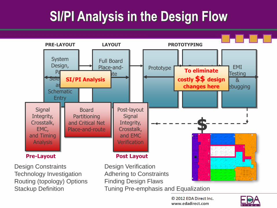
SI/PI Analysis in the Design Flow
System Design,
Part Selection
and Schematic
Entry
Prototype
PRE-LAYOUT LAYOUT
Full BoardPlace-and-
route
$
FunctionalTesting
&Debugging
PROTOTYPING
EMITesting
&Debugging
Signal Integrity, Crosstalk,
EMC,and Timing
Analysis
Board Partitioning
and Critical NetPlace-and-route
Post-layoutSignal
Integrity, Crosstalk, and EMC
Verification
Pre-Layout Post Layout
SI/PI Analysis
To eliminate
costly $$ design
changes here
Design Constraints
Technology Investigation
Routing (topology) Options
Stackup Definition
Design Verification
Adhering to Constraints
Finding Design Flaws
Tuning Pre-emphasis and Equalization

www.edadirect.comFrom-Concept-to-Chip-to-Board © 2014 | 4
High-speed PCB Design Issues
• Signal Integrity
– General interfaces
• Timing, crosstalk, signal quality
– DDRx
• Full STA, slew rate derating, write leveling
– SERDES
• Loss, impedance discontinuities, BER prediction
• Power Integrity
– DC : do I have enough metal?
• Voltage drop, high current density, neckdowns
– AC : do I have enough caps? values?
• Well-mounted? Good stackup?
• Impedance profile, noise propagation
• EMI/EMC
– Emission Regulations

www.edadirect.comFrom-Concept-to-Chip-to-Board © 2014 | 5
Setup/planning – Board Stackup Design
• Signal Integrity
– Impedance• Highest impedance will drive layer thicknesses
• Need reference planes for uniform impedance
– Loss• Drives trace widths –> layer thicknesses
– Crosstalk• Drives spacing requirements and routing density
• Power Integrity
– Need enough thick planes to minimize DC drop
– Need closely-spaced plane pairs for AC needs
– Need stitching vias to relieve current choke points
• EMI/EMC
– Need solid reference planes throughout stackup
capacitor

www.edadirect.comFrom-Concept-to-Chip-to-Board © 2014 | 6
• Layout/Route
– Avoid crossing splits in reference planes (discontinuities)
– Minimize Inter Symbol Interference (ISI) using matched Impedances
– Minimize Crosstalk by isolating sensitive bits (ie. Strobes)
– Match traces within byte lanes (DQ, DM, DQS) to minimize skews
• Power Supplies
– Use precision resistors for VREF
– Short/Wide traces to minimize L and loss
– 15~25mil clearance from VREF to adjacent traces to minimize coupling
– Decouple high frequency Power Supply noise w/caps
• Signaling
– DQ Driver Impedance Matching with proper drive strengths
– ODT is a must for better Signal Integrity (if not used then use T-branches or dumping resistor to minimize reflections
– Choose termination carefully to balance power consumption, signal swing, and reflection
– Use 2T timing for Address/Command
Design Considerations

www.edadirect.comFrom-Concept-to-Chip-to-Board © 2014 | 7
Signal Integrity Crosstalk EMC
Signal Integrity Analysis
Sweep Parameters Impedance/Stackup Planning Multi-Board
Eye Diagrams

www.edadirect.comFrom-Concept-to-Chip-to-Board © 2014 | 8
DDRx Fly-By Topology – Write Leveling
• Controller Delays DQ signals internally
• DQ & DQS signals are sent “Level” with the Addr/CLK

www.edadirect.comFrom-Concept-to-Chip-to-Board © 2014 | 9
Overview – DDR3 vs. DDR4
DDR3 DDR4 Comments
VDD/VDDQ/VPP 1.5/1.5/NA
(1.35/1.35/NA)
1.2/1.2/2.5 Up to 20% power saving
Clock Frequencies 400-1600MHz 800-1600MHz+ Higher BW
CAS Latency 5~14 9~24
Vref VDDQ/2 (Ext) Internal
DQ Validation Setup/Hold Data Eye Borrowed from SERDES
Data Termination VDDQ/2 (VTT) VDDQ Asymmetric Term.
Add/Cmd/Termination VDDQ/2 (VTT) VDDQ/2
I/O Standard SSTL15 POD12 Power savings on “1” bits
On Chip Error Detection No Parity (Cmd/Add)
CRC (DQ)
Server Class
Bank Grouping No 4 “Ping-Pong” for efficient use
www.edadirect.comFrom-Concept-to-Chip-to-Board © 2014 | 10
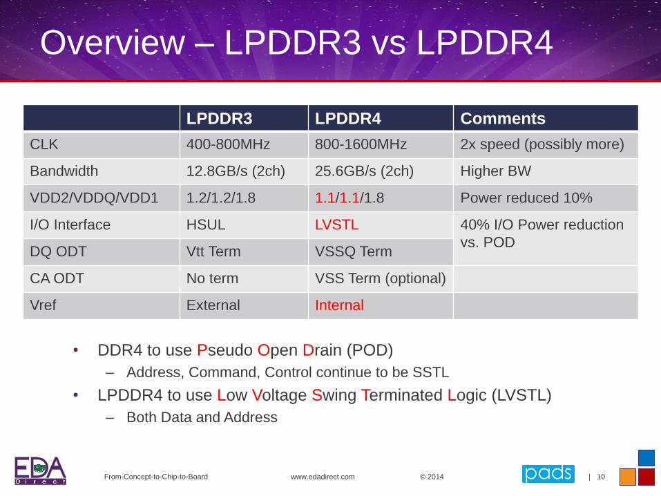
Overview – LPDDR3 vs LPDDR4
LPDDR3 LPDDR4 Comments
CLK 400-800MHz 800-1600MHz 2x speed (possibly more)
Bandwidth 12.8GB/s (2ch) 25.6GB/s (2ch) Higher BW
VDD2/VDDQ/VDD1 1.2/1.2/1.8 1.1/1.1/1.8 Power reduced 10%
I/O Interface HSUL LVSTL 40% I/O Power reduction
vs. PODDQ ODT Vtt Term VSSQ Term
CA ODT No term VSS Term (optional)
Vref External Internal
• DDR4 to use Pseudo Open Drain (POD)
– Address, Command, Control continue to be SSTL
• LPDDR4 to use Low Voltage Swing Terminated Logic (LVSTL)
– Both Data and Address

www.edadirect.comFrom-Concept-to-Chip-to-Board © 2014 | 11
Overview – Speed related Eye challenges
Semicon West: High Performance & Low Power Memory Trends – SK Hynix

www.edadirect.comFrom-Concept-to-Chip-to-Board © 2014 | 12
New Drive Standards – Difference
DDR4
DDR3

www.edadirect.comFrom-Concept-to-Chip-to-Board © 2014 | 13
New Drive Standards – Why?
• Current still flows when driving low
I
I
DDR4
DDR3

www.edadirect.comFrom-Concept-to-Chip-to-Board © 2014 | 14
New Drive Standards – Why?
• No current draw when driving a high
I
No
Current DDR4
DDR3

www.edadirect.comFrom-Concept-to-Chip-to-Board © 2014 | 15
Power Savings with DBI
• Ensure more 1’s than 0’s with POD
• If more than 4 bits in a byte are 0, toggle bits
• DBI (Data Bit Inversion) shared with DM => only one
feature enabled
• DBI pin is I/O (affects both reads and writes)

www.edadirect.comFrom-Concept-to-Chip-to-Board © 2014 | 16
PreLayout SI Simulation

www.edadirect.comFrom-Concept-to-Chip-to-Board © 2014 | 17
DDRx Routing Guidelines
• Constraint-driven routing
– Designer knows where the traces
should be routed
• Precise location of traces & vias
• Control style of routing incl serpentines
– Things to observe while routing DDRx• Width & clearance rules
• Placement intentions
• Netline organization
• Layer restrictions
• Pad/via entry rules (angle, size)
• Diff pair rules
17

www.edadirect.comFrom-Concept-to-Chip-to-Board © 2014 | 18
Using Sketch routing with DDR3 (video)

www.edadirect.comFrom-Concept-to-Chip-to-Board © 2014 | 19
Simple Comparison
• Controller -> 50 Ohm T-Line -> DRAM
• Vary DRAM’s ODT to see center level of eye
• 2400Mbps Data rate

www.edadirect.comFrom-Concept-to-Chip-to-Board © 2014 | 20
DDR3 – sweeping Rx ODT
No change in Center of Eye with ODT

www.edadirect.comFrom-Concept-to-Chip-to-Board © 2014 | 21
DDR4 – Eye shifting
Eye center shifts with ODT change

www.edadirect.comFrom-Concept-to-Chip-to-Board © 2014 | 22
LPDDR4 – Eye shifting
Eye center shifts with ODT change

www.edadirect.comFrom-Concept-to-Chip-to-Board © 2014 | 23
Xilinx VCU108 UltraScale Dev Board

www.edadirect.comFrom-Concept-to-Chip-to-Board © 2014 | 24
Altera Aria10GX FPGA Dev Board
DDR4 Module

www.edadirect.comFrom-Concept-to-Chip-to-Board © 2014 | 25
What is Power Integrity?
• What is a Power Distribution Network (PDN)?
– The path (or interconnects) from PWR to ICs (Active Devices)
– Including PCBs and packages
• Planes, routed traces, and decoupling capacitors
• Deliver adequate power from DC->HF
• Minimize EMI issues
• Provide low-noise reference path for signaling
VRMPCB
Bypass capacitor
Active device
Power planes
Test point 2 Test point 1

www.edadirect.comFrom-Concept-to-Chip-to-Board © 2014 | 26
Plane Design & the PDN
• Meeting Power Integrity requirements
– Design PDN (path from power supply to ICs) of low impedance
• As if an ideal voltage source were directly connected to ICs
– Use impedance to represent and measure PDN quality
Die
PCB
Package
Chip to Package Bumps
Package to Board Bump and/or Connectors
PCB Routing
Power Delivery Path

www.edadirect.comFrom-Concept-to-Chip-to-Board © 2014 | 27
Power Integrity Analysis
• DC Drop Analysis
– Excessive Voltage Drop & High
Current Densities
– Batch Analysis of Supply Nets
• AC Power Plane Analysis
– Capacitor Selection/Mounting
– Power Supply Impedance
• Plane Noise Analysis
– Voltage Ripples

www.edadirect.comFrom-Concept-to-Chip-to-Board © 2014 | 28
Reduce Product Costs
— Minimizing capacitor BOM (more Caps is worse)
— Reducing PCB size and layer count
— Eliminating design iterations
– Up-front PDN planning & Improve time-to-results
Improve Product Reliability
— Identifying excessive voltage drop and high current
densities at DC
— Providing stable AC power through capacitor
decoupling
Power Integrity Optimization (Why?)

www.edadirect.comFrom-Concept-to-Chip-to-Board © 2014 | 29
DC Drop and Thermal Analysis
• Identify Failures Easily
– Voltage drop magnitude is
easily measured
– Excessive current density is identified
clearly
– Determine if current density is
causing thermal failure
• Create an Optimized Solution
– How much copper is needed?
– Optimize component placement?
– Are additional stitching vias required?
www.edadirect.comFrom-Concept-to-Chip-to-Board © 2014 | 30
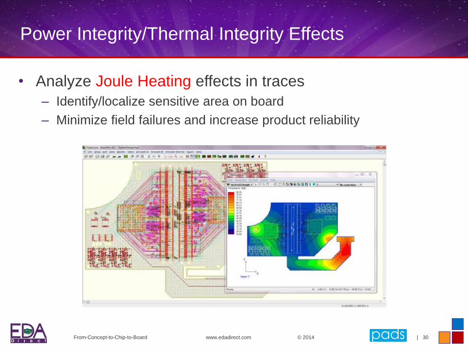
Power Integrity/Thermal Integrity Effects
• Analyze Joule Heating effects in traces
– Identify/localize sensitive area on board
– Minimize field failures and increase product reliability

www.edadirect.comFrom-Concept-to-Chip-to-Board © 2014 | 31
Power Integrity Effects

www.edadirect.comFrom-Concept-to-Chip-to-Board © 2014 | 32
PDN From
DDR3 Board
Signal held high
Remaining signals
PRBS @ 2400MT/s
DQS clock @ 1.2GHz
Power Integrity Effects from DDR3 switching

www.edadirect.comFrom-Concept-to-Chip-to-Board © 2014 | 33
Power Integrity Effects from DDR3 switching
150mV noise from switching of other bits in lane

www.edadirect.comFrom-Concept-to-Chip-to-Board © 2014 | 34
Integrated Design Flow
SI/PI/Thermal
Simulation
Pre/Post
Schematic
Design
Board
Layout/Route
Constraints
Constraints
Constraints
Library/Symbols
Design Variants
Architectural/Technology Investigation
Performance/Feasibility Analysis
Noise/Crosstalk/Termination/EMI
Stackup/Placements
Length/Impedance/via
• Tight validation for Pre/Post Layout
• Minimize errors, increase accuracy
• Reduce risk and field failures
• Lower cost and reduce time-to-market

www.edadirect.comFrom-Concept-to-Chip-to-Board © 2014 | 35
Contact Info
EDA Direct Inc.
(408) 496-5890
(888) 669-9EDA
To enroll for our upcoming seminars, workshops, training classes,
and view demo videos of our products
visit www.edadirect.com