high-speed usb on-the-go ulpi transceiver - stm32 · september 2010 doc id 14817 rev 2 1/44 1...
TRANSCRIPT

September 2010 Doc ID 14817 Rev 2 1/44
1
STULPI01ASTULPI01B
High-speed USB on-the-go ULPI transceiver
Features■ USB-IF high speed certified to the Universal
Serial Bus specification rev 2.0
■ Meets the requirements of the Universal Serial Bus specification revision 2.0, on-the-go supplement to the USB 2.0 specification 1.0a and ULPI transceiver specification 1.1
■ Standard ULPI (UTMI+ low pin interface) 1.1 digital interface
■ Fully compliant with ULPI 1.1 register set
■ External square wave clock with DVIO amplitude must be applied to oscillator input XI
■ Supports 480 Mbit/s high-speed, 12 Mbit/s full-speed and 1.5 Mbit/s low-speed modes of operation
■ Supports 2.7 V UART mode.
■ Supports session request protocol (SRP) and host negotiation protocol (HNP) for dual-role device features
■ Ability to control external charge pump for higher VBUS currents.
■ Single supply, +3 V to +4.5 V voltage range
■ Integrated dual voltage regulator to supply internal circuits with stable 3.3 V and 1.2 V
■ Integrated overcurrent detector
■ Integrated HS termination and FS/LS/OTG pull-up/pull-down resistors
■ Integrated USB 2.0 “short-circuit withstand” protection
■ Power-down mode with very low power consumption for battery-powered devices
■ Ideal for system ASICs with built-in USB host, device or OTG cores
■ Available in µTFBGA36 RoHS package
■ –40 °C to 85 °C operating temperature range
Applications■ Mobile phones
■ PDAs
■ MP3 players
■ Digital still cameras
■ Set-top box
■ Portable navigation devices
DescriptionThe STULPI01 is a high-speed USB 2.0 transceiver compliant with ULPI (UTMI+ low pin interface) and OTG (on-the-go) specifications, providing a complete physical layer solution for any high-speed USB host, device or OTG dual-role core. It allows USB ASICs to interface with the physical layer of the USB through a 12-pin interface. It contains VBUS comparators, an ID line detector, USB differential drivers and receivers and a complete ULPI register map and interrupt generator. The STULPI01 transceiver is suitable for mobile applications and battery-powered devices because of its low power consumption, power-down operating mode and minimal die/package dimensions.
µTFBGA36
www.st.com

Contents STULPI01A - STULPI01B
2/44 Doc ID 14817 Rev 2
Contents
1 Application diagrams . . . . . . . . . . . . . . . . . . . . . . . . . . . . . . . . . . . . . . . . 6
2 Bump configuration . . . . . . . . . . . . . . . . . . . . . . . . . . . . . . . . . . . . . . . . . 7
3 Maximum ratings . . . . . . . . . . . . . . . . . . . . . . . . . . . . . . . . . . . . . . . . . . . . 9
4 Electrical characteristics . . . . . . . . . . . . . . . . . . . . . . . . . . . . . . . . . . . . 10
5 Timing diagram . . . . . . . . . . . . . . . . . . . . . . . . . . . . . . . . . . . . . . . . . . . . 17
6 Block description . . . . . . . . . . . . . . . . . . . . . . . . . . . . . . . . . . . . . . . . . . 18
6.1 Oscillator and PLL . . . . . . . . . . . . . . . . . . . . . . . . . . . . . . . . . . . . . . . . . . 18
6.2 Voltage reference . . . . . . . . . . . . . . . . . . . . . . . . . . . . . . . . . . . . . . . . . . . 18
6.3 Power-on-reset (POR) . . . . . . . . . . . . . . . . . . . . . . . . . . . . . . . . . . . . . . . 18
6.4 UTMI + CORE . . . . . . . . . . . . . . . . . . . . . . . . . . . . . . . . . . . . . . . . . . . . . 18
6.5 ULPI wrapper . . . . . . . . . . . . . . . . . . . . . . . . . . . . . . . . . . . . . . . . . . . . . . 18
6.6 External charge pump . . . . . . . . . . . . . . . . . . . . . . . . . . . . . . . . . . . . . . . 19
6.7 VBUS comparators and VBUS overcurrent (OC) detector . . . . . . . . . . . . 19
6.8 VB_REF_FAULT pin . . . . . . . . . . . . . . . . . . . . . . . . . . . . . . . . . . . . . . . . . 19
6.9 Voltage regulator . . . . . . . . . . . . . . . . . . . . . . . . . . . . . . . . . . . . . . . . . . . 20
6.10 ID detector . . . . . . . . . . . . . . . . . . . . . . . . . . . . . . . . . . . . . . . . . . . . . . . . 20
6.11 USB 2.0 PHY . . . . . . . . . . . . . . . . . . . . . . . . . . . . . . . . . . . . . . . . . . . . . . 20
6.12 Power saving features . . . . . . . . . . . . . . . . . . . . . . . . . . . . . . . . . . . . . . . 21
6.13 Modes of operation . . . . . . . . . . . . . . . . . . . . . . . . . . . . . . . . . . . . . . . . . . 21
6.13.1 ULPI synchronous mode . . . . . . . . . . . . . . . . . . . . . . . . . . . . . . . . . . . . 21
6.13.2 6-pin FS/LS serial mode . . . . . . . . . . . . . . . . . . . . . . . . . . . . . . . . . . . . 21
6.13.3 3-pin FS/LS serial mode . . . . . . . . . . . . . . . . . . . . . . . . . . . . . . . . . . . . 21
6.14 Car kit (UART) mode . . . . . . . . . . . . . . . . . . . . . . . . . . . . . . . . . . . . . . . . 21
6.15 Low-power mode . . . . . . . . . . . . . . . . . . . . . . . . . . . . . . . . . . . . . . . . . . . 22
6.16 Power-down mode . . . . . . . . . . . . . . . . . . . . . . . . . . . . . . . . . . . . . . . . . . 23
6.17 VIO OFF mode . . . . . . . . . . . . . . . . . . . . . . . . . . . . . . . . . . . . . . . . . . . . . 23
6.18 Startup procedure . . . . . . . . . . . . . . . . . . . . . . . . . . . . . . . . . . . . . . . . . . 23
6.18.1 ULPI device detection . . . . . . . . . . . . . . . . . . . . . . . . . . . . . . . . . . . . . . 23

STULPI01A - STULPI01B Contents
Doc ID 14817 Rev 2 3/44
6.18.2 SDR mode selection . . . . . . . . . . . . . . . . . . . . . . . . . . . . . . . . . . . . . . . 23
6.18.3 External clock detection . . . . . . . . . . . . . . . . . . . . . . . . . . . . . . . . . . . . . 24
6.18.4 Reset behavior . . . . . . . . . . . . . . . . . . . . . . . . . . . . . . . . . . . . . . . . . . . . 24
6.18.5 Interface protection . . . . . . . . . . . . . . . . . . . . . . . . . . . . . . . . . . . . . . . . 24
6.18.6 Software reset . . . . . . . . . . . . . . . . . . . . . . . . . . . . . . . . . . . . . . . . . . . . 24
6.18.7 High-speed mode entry . . . . . . . . . . . . . . . . . . . . . . . . . . . . . . . . . . . . . 25
7 State transitions . . . . . . . . . . . . . . . . . . . . . . . . . . . . . . . . . . . . . . . . . . . 28
8 ULPI registers . . . . . . . . . . . . . . . . . . . . . . . . . . . . . . . . . . . . . . . . . . . . . 30
9 Package mechanical data . . . . . . . . . . . . . . . . . . . . . . . . . . . . . . . . . . . . 39
10 Order codes . . . . . . . . . . . . . . . . . . . . . . . . . . . . . . . . . . . . . . . . . . . . . . 42
11 Revision history . . . . . . . . . . . . . . . . . . . . . . . . . . . . . . . . . . . . . . . . . . . 43

List of tables STULPI01A - STULPI01B
4/44 Doc ID 14817 Rev 2
List of tables
Table 1. Bill of materials - external components . . . . . . . . . . . . . . . . . . . . . . . . . . . . . . . . . . . . . . . . . 6Table 2. Pinout and bump description . . . . . . . . . . . . . . . . . . . . . . . . . . . . . . . . . . . . . . . . . . . . . . . . 7Table 3. Absolute maximum ratings . . . . . . . . . . . . . . . . . . . . . . . . . . . . . . . . . . . . . . . . . . . . . . . . . . 9Table 4. Thermal data. . . . . . . . . . . . . . . . . . . . . . . . . . . . . . . . . . . . . . . . . . . . . . . . . . . . . . . . . . . . . 9Table 5. Recommended operating conditions . . . . . . . . . . . . . . . . . . . . . . . . . . . . . . . . . . . . . . . . . . 9Table 6. Electrical characteristics . . . . . . . . . . . . . . . . . . . . . . . . . . . . . . . . . . . . . . . . . . . . . . . . . . . 10Table 7. Switching characteristics . . . . . . . . . . . . . . . . . . . . . . . . . . . . . . . . . . . . . . . . . . . . . . . . . . 14Table 8. High-speed driver eye pattern . . . . . . . . . . . . . . . . . . . . . . . . . . . . . . . . . . . . . . . . . . . . . . 16Table 9. VB_REF_FAULT configuration bit settings. . . . . . . . . . . . . . . . . . . . . . . . . . . . . . . . . . . . . 20Table 10. Car kit signals mapping . . . . . . . . . . . . . . . . . . . . . . . . . . . . . . . . . . . . . . . . . . . . . . . . . . . 22Table 11. Low-power mode . . . . . . . . . . . . . . . . . . . . . . . . . . . . . . . . . . . . . . . . . . . . . . . . . . . . . . . . 23Table 12. USB state transitions . . . . . . . . . . . . . . . . . . . . . . . . . . . . . . . . . . . . . . . . . . . . . . . . . . . . . 28Table 13. ULPI register map overview . . . . . . . . . . . . . . . . . . . . . . . . . . . . . . . . . . . . . . . . . . . . . . . . 30Table 14. Register access legend . . . . . . . . . . . . . . . . . . . . . . . . . . . . . . . . . . . . . . . . . . . . . . . . . . . 30Table 15. Vendor and product ID . . . . . . . . . . . . . . . . . . . . . . . . . . . . . . . . . . . . . . . . . . . . . . . . . . . . 31Table 16. Power control register . . . . . . . . . . . . . . . . . . . . . . . . . . . . . . . . . . . . . . . . . . . . . . . . . . . . . 31Table 17. Function control register . . . . . . . . . . . . . . . . . . . . . . . . . . . . . . . . . . . . . . . . . . . . . . . . . . . 32Table 18. Interface control register . . . . . . . . . . . . . . . . . . . . . . . . . . . . . . . . . . . . . . . . . . . . . . . . . . . 33Table 19. OTG control register . . . . . . . . . . . . . . . . . . . . . . . . . . . . . . . . . . . . . . . . . . . . . . . . . . . . . . 34Table 20. USB interrupt enable rising register . . . . . . . . . . . . . . . . . . . . . . . . . . . . . . . . . . . . . . . . . . 35Table 21. USB interrupt enable falling register . . . . . . . . . . . . . . . . . . . . . . . . . . . . . . . . . . . . . . . . . . 36Table 22. USB interrupt status register. . . . . . . . . . . . . . . . . . . . . . . . . . . . . . . . . . . . . . . . . . . . . . . . 36Table 23. USB interrupt latch register. . . . . . . . . . . . . . . . . . . . . . . . . . . . . . . . . . . . . . . . . . . . . . . . . 37Table 24. Setting rules for interrupt latch register . . . . . . . . . . . . . . . . . . . . . . . . . . . . . . . . . . . . . . . . 37Table 25. Debug register . . . . . . . . . . . . . . . . . . . . . . . . . . . . . . . . . . . . . . . . . . . . . . . . . . . . . . . . . . 38Table 26. Scratch register. . . . . . . . . . . . . . . . . . . . . . . . . . . . . . . . . . . . . . . . . . . . . . . . . . . . . . . . . . 38Table 27. Carkit control register . . . . . . . . . . . . . . . . . . . . . . . . . . . . . . . . . . . . . . . . . . . . . . . . . . . . . 38Table 28. Order codes . . . . . . . . . . . . . . . . . . . . . . . . . . . . . . . . . . . . . . . . . . . . . . . . . . . . . . . . . . . . 42Table 29. Document revision history . . . . . . . . . . . . . . . . . . . . . . . . . . . . . . . . . . . . . . . . . . . . . . . . . 43

STULPI01A - STULPI01B List of figures
Doc ID 14817 Rev 2 5/44
List of figures
Figure 1. Peripheral only, configuration with external clock . . . . . . . . . . . . . . . . . . . . . . . . . . . . . . . . . 6Figure 2. Pin connections . . . . . . . . . . . . . . . . . . . . . . . . . . . . . . . . . . . . . . . . . . . . . . . . . . . . . . . . . . 7Figure 3. High-speed driver eye pattern . . . . . . . . . . . . . . . . . . . . . . . . . . . . . . . . . . . . . . . . . . . . . . 16Figure 4. Rise and fall time . . . . . . . . . . . . . . . . . . . . . . . . . . . . . . . . . . . . . . . . . . . . . . . . . . . . . . . . 17Figure 5. Simplified block diagram. . . . . . . . . . . . . . . . . . . . . . . . . . . . . . . . . . . . . . . . . . . . . . . . . . . 17Figure 6. VB_REF_FAULT pin functionality. . . . . . . . . . . . . . . . . . . . . . . . . . . . . . . . . . . . . . . . . . . . 19Figure 7. USB 2.0 PHY block diagram. . . . . . . . . . . . . . . . . . . . . . . . . . . . . . . . . . . . . . . . . . . . . . . . 21Figure 8. Startup sequence . . . . . . . . . . . . . . . . . . . . . . . . . . . . . . . . . . . . . . . . . . . . . . . . . . . . . . . . 25Figure 9. RESETn behavior . . . . . . . . . . . . . . . . . . . . . . . . . . . . . . . . . . . . . . . . . . . . . . . . . . . . . . . . 25Figure 10. High-speed mode entry . . . . . . . . . . . . . . . . . . . . . . . . . . . . . . . . . . . . . . . . . . . . . . . . . . . 26Figure 11. UARTmode entry (2.7 V) . . . . . . . . . . . . . . . . . . . . . . . . . . . . . . . . . . . . . . . . . . . . . . . . . . 26Figure 12. UART mode exit (2.7 V) . . . . . . . . . . . . . . . . . . . . . . . . . . . . . . . . . . . . . . . . . . . . . . . . . . . 27

Application diagrams STULPI01A - STULPI01B
6/44 Doc ID 14817 Rev 2
1 Application diagrams
Figure 1. Peripheral only, configuration with external clock
AM04944v1
DVIO
DVIO
DVIO
CLKDIRSTPNXT
D[0]...D[7]
RESETn
CSn / PWRDN
3V3V 1V2VVBAT
XI
External clock19.2/26 MHzDVIO amplitutde
XO
IDDPDM
VBUS
RREF
PSWn
VB_REF_FAULT
5x GND
Table 1. Bill of materials - external components
Qty Symbol Value Description
1 CF1 0.1 - 1 µF
Filtering capacitor. Suggested components:muRata 10 V X5R (GRM188R61A105KA61) or muRata 10 V Y5V (GRM188F51A105ZA01) orTaiyo Yuden 25V X5R (TMK107BJ105KA)
2 CF4 0.1 - 1 µF
Filtering capacitor. Suggested components:muRata 10 V X5R (GRM188R61A105KA61) or muRata 10 V Y5V (GRM188F51A105ZA01) orTaiyo Yuden 25V X5R (TMK107BJ105KA)
1 CF2 1µF - 1.5 µF
Filtering capacitor. Suggested components:muRata 10 V X5R (GRM188R61A105KA61) or muRata 10 V Y5V (GRM188F51A105ZA01) orTaiyo Yuden 25V X5R (TMK107BJ105KA)
1 CF3 1 - 4.7 µFFiltering capacitor. Suggested components:muRata 10 V Y5V (GRM188F51A475ZE20) orTaiyo Yuden 6.3 V X5R (JMK107BJ475KA)
1 CT 4.7 µF Tank capacitor
1 RREF 12 kΩ Reference resistor ±1%
1 E1 USBULC6-2F3
1 E2 ESDA14V2-2BF3
1 RBUS 2.2 kΩ Series overvoltage protection resistor
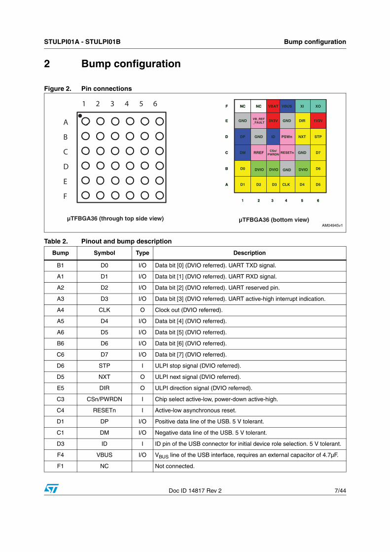
STULPI01A - STULPI01B Bump configuration
Doc ID 14817 Rev 2 7/44
2 Bump configuration
Figure 2. Pin connections
µTFBGA36 (bottom view)
A
B
C
D
E
F
1 2 3 4 5 6
µTFBGA36 (through top side view)
654321
D5D4CLKD3D2D1A
D61V8VIO
GND1V8VIO
1V8VIO
D0B
D7GNDRESETnCSn/PWRDNRREFDMC
STPNXTPSWnIDGNDDPD
1V2VDIRGND3V3VVB_REF_FAULTGNDE
XOXIVBUSVBATNCNCF
654321
D5D4CLKD3D2D1A
D6GNDDVIOD0B
D7GNDRESETnCSn/PWRDNRREFDMC
STPNXTPSWnIDGNDDPD
1V2VDIRGND3V3VVB_REF_FAULTGNDE
XOXIVBUSVBATNCNCF
AM04945v1
DVIO DVIO
Table 2. Pinout and bump description
Bump Symbol Type Description
B1 D0 I/O Data bit [0] (DVIO referred). UART TXD signal.
A1 D1 I/O Data bit [1] (DVIO referred). UART RXD signal.
A2 D2 I/O Data bit [2] (DVIO referred). UART reserved pin.
A3 D3 I/O Data bit [3] (DVIO referred). UART active-high interrupt indication.
A4 CLK O Clock out (DVIO referred).
A5 D4 I/O Data bit [4] (DVIO referred).
A6 D5 I/O Data bit [5] (DVIO referred).
B6 D6 I/O Data bit [6] (DVIO referred).
C6 D7 I/O Data bit [7] (DVIO referred).
D6 STP I ULPI stop signal (DVIO referred).
D5 NXT O ULPI next signal (DVIO referred).
E5 DIR O ULPI direction signal (DVIO referred).
C3 CSn/PWRDN I Chip select active-low, power-down active-high.
C4 RESETn I Active-low asynchronous reset.
D1 DP I/O Positive data line of the USB. 5 V tolerant.
C1 DM I/O Negative data line of the USB. 5 V tolerant.
D3 ID I ID pin of the USB connector for initial device role selection. 5 V tolerant.
F4 VBUS I/O VBUS line of the USB interface, requires an external capacitor of 4.7µF.
F1 NC Not connected.

Bump configuration STULPI01A - STULPI01B
8/44 Doc ID 14817 Rev 2
F2 NC Not connected.
E2 VB_REF_FAULT IVoltage reference for internal OC detector input or digital input from external OC detector (V3V3V referred). 5 V tolerant.
D4 PSWn O External charge pump control, active low. 5 V tolerant, open drain.
F5 XI I External clock input (DVIO referred). Crystal terminal (on request).
F6 XO OLeft floating or connect to GND when external clock signal is used. Crystal terminal on request.
F3 VBAT PWRBattery power input for the LDO (3 V – 4.5 V). Bypass VBAT to GND with a 1 µF capacitor.
E3 3V3V PWR 3.3 V LDO output. Bypass 3V3V to GND with a 1.5 µF capacitor.
E6 1V2V PWR 1.2 V LDO output. Bypass 1V2V to GND with a 1.5 µF capacitor.
C2 RREF I/O Reference resistor (12 kΩ ±1%).
B2/B3/B5 DVIO PWRDigital I/O supply voltage. Bypass each DVIO to GND with a 100 nF-1 uF capacitor. Balls B2-B5 can share common capacitor.
C5/D2 GND PWR Ground.
B4/E4/E1 GND PWR Ground.
Table 2. Pinout and bump description (continued)

STULPI01A - STULPI01B Maximum ratings
Doc ID 14817 Rev 2 9/44
3 Maximum ratings
Note: Absolute maximum ratings are those values above which damage to the device may occur. Functional operation under these conditions is not implied. All voltages are referenced to GND.
Table 3. Absolute maximum ratings
Symbol Parameter Value Unit
VDVIO Digital I/O supply voltage -0.3 to +4.0 V
V1V2 Digital core supply voltage (provided internally by LDO) -0.3 to +1.4 V
V3V3 Analog supply voltage (provided internally by LDO) -0.3 to +4.0 V
VBAT Battery supply voltage -0.3 to +7.0 V
VDCDIG DC voltage on digital pins (CLK, DIR, STP, NXT, D[0-7], RESETn) -0.3 to +2.0 V
VDCANA DC voltage on analog pins (XI, XO, PSWn) -0.3 to +4.0 V
VDCVBUS DC voltage on 5 V tolerant pins (VBUS,VB_REF_FAULT, DP, DM, ID) -0.3 to +5.5 V
TSTG Storage temperature range -40 to +125 °C
VESD-HBMElectrostatic discharge voltage on all pins (according to JESD22-A114-B)
±2.0 kV
Table 4. Thermal data
Symbol Parameter Value Unit
RthJA Thermal resistance junction-ambient (simulated value as per JEDEC JSD51) 113.8 °C/W
RthJC Thermal resistance junction-case (simulated value as per JEDEC JSD51) 47 °C/W
RthJB Thermal resistance junction-base (simulated value as per JEDEC JSD51) 66.2 °C/W
Table 5. Recommended operating conditions
Symbol Parameter Min. Typ. Max. Unit
VBAT Battery supply voltage 3.0 3.6 4.5 V
VDVIO Digital I/O supply voltage 1.65 1.80 3.6 V
TA Operating temperature range -40 +85 °C
CT Tank capacitor 1 4.7 6.5 µF
RREF External reference resistor 11.88 12 12.12 kΩ
XTALExternal square wave (01A, 01B versions) 19.2 or 26 MHz
Recommended rise/fall time 4 ns

Electrical characteristics STULPI01A - STULPI01B
10/44 Doc ID 14817 Rev 2
4 Electrical characteristics
Table 6. Electrical characteristics
Characteristics measured over recommended operating conditions unless otherwise noted. All typical values are referred to TA = 25 °C, VDVIO = 1.8 V, VBAT = 3.6 V, RREF = 12 kΩ; CT = 4.7 µF)
Symbol Parameter Test conditions Min. Typ. Max. Unit
Power consumption
IBAT Supply current
Active mode (USB bus idle) 15 mA
Active mode (FS transmission, 12 Mb/s traffic)
30 mA
Active mode (HS transmission)
50 mA
Suspend mode (not including DP pull-up current, external clock stopped)
120 µA
UART mode (no transmission)
15 mA
Power down mode 0.4 2 µA
VIO OFF mode (DVIO = 0) 0.4 2 µA
IDVIOULPI bus supply current DVIO
Power down mode 0.1 10 µA
Active mode, 4 pF load 1.8 mA
Logic inputs and outputs
CULPIIN ULPI port I/O capacitance 2.4 3.5 pF
VOHHigh level output voltage (ULPI bus)
IOH = -2 mA VDVIO-0.15 V
VOLLow level output voltage (ULPI bus)
IOL = +2 mA 0.15 V
IOZH_PSWnHigh level output leakage (PSWn)
VOH_PSWn = 3.3 V power switch disabled
1.0 µA
VOL_PSWnLow level output voltage (PSWn)
IOL = +2 mA power switch enabled
0.15 V
VIHHigh level input voltage (ULPI port and RESETn)
0.65xVDVIO V
VILLow level input voltage (ULPI port and RESETn)
0.35xVDVIO V
IIHHigh level input leakage current
VIH = VDVIO-0.2 V ±1.0 µA

STULPI01A - STULPI01B Electrical characteristics
Doc ID 14817 Rev 2 11/44
Symbol Parameter Test conditions Min. Typ. Max. Unit
IILLow level input leakage cur-rent
VIL = 0.2 V ±1.0 µA
VPDHHigh level input voltage (CSn/PWRDN pin)
VBAT = 3.0 V to 4.5 V 1.4 V
VPDLLow level input voltage (CSn/PWRDN pin)
VBAT = 3.0 V to 4.5 V 0.4 V
IPDHHigh level input leakage current (CSn/PWRDN pin)
VPD = 1.4 V, VBAT = 4.5 V ±1.0 µA
IPDLLow level input leakage current (CSn/PWRDN pin)
VPD = 0.4 V, VBAT = 4.5 V ±1.0 µA
VFAULTHHigh level input voltage (VB_REF_FAULT pin)
Overcurrent_PD bit is set 0.65xV3V3 V
VFAULTLLow level input voltage (VB_REF_FAULT pin)
Overcurrent_PD bit is set 0.15xV3V3 V
RIN_VB_REFVB_REF_FAULT pin input resistance
112 148 168 kΩ
VXI_HYST_E
XT
External clock input hysteresis
XO = ‘0’ @ reset 500 mV
VXIHHigh level input voltage (XI pin)
XO = ‘0’ @ reset 0.65xVDVIO V
VXILLow level input voltage (XI pin)
XO = ‘0’ @ reset 0.15xVDVIO V
VBUS
VBUS_LKG VBUS leakage voltage No load 200 mV
RVBUS VBUS input impedance 40 100 kΩ
VBUS_VLDVBUS valid comparator threshold
1 kΩ series resistors 4.4 4.75 V
VSESS_VLD
Session valid comparator threshold for both A and B device
Low to high transition 0.8 1.45 2.0 V
High to low transition 1.25 V
VSESS_ENDSession end comparator threshold
0.2 0.8 V
RVBUS_PUVBUS charge pull-up resistance
650 950 1150 Ω
RVBUS_PDVBUS discharge pull-down resistance
800 1250 1500 Ω
Table 6. Electrical characteristics (continued)
Characteristics measured over recommended operating conditions unless otherwise noted. All typical values are referred to TA = 25 °C, VDVIO = 1.8 V, VBAT = 3.6 V, RREF = 12 kΩ; CT = 4.7 µF)

Electrical characteristics STULPI01A - STULPI01B
12/44 Doc ID 14817 Rev 2
Symbol Parameter Test conditions Min. Typ. Max. Unit
Overcurrent detector
VOCOver current trip threshold VB_REF_FAULT – VBUS
VOC = VB_REF_FAULT – VBUS
20 45 95 mV
ID
IID_PU ID pin pull-up current VID = 0V 70 µA
RID_GNDID line short resistance to detect ID GND state
1 kΩ
RID_FLOATID line short resistance to detect ID FLOAT state
100 kΩ
UART mode (2.7 V ± 5 %)
VOH_UARTHigh level output voltage (D1,D3)
IOH = -2 mA VDVIO-0.15 V
VOL_UARTLow level output voltage (D1,D3)
IOL = +2 mA 0.15 V
VIH_UART_D
0
High level input voltage (D0)
0.65xVDVIO V
VIL_UART_D0 Low level input voltage (D0) 0.35xVDVIO V
VOH_DFMSHigh level output voltage (DP)
IOH = -2 mA 2.16 2.85 V
VOL_DFMSLow level output voltage (DP)
IOL = +2 mA, Pull-up=10kΩ -0.10 0.37 V
VIH_DTMSHigh level input voltage (DM)
2.0 3.0 V
VIL_DTMSLow level input voltage (DM)
-0.3 0.81 V
Full-speed/low-speed driver
ZDRV
Output impedance (acting also as high-speed termination)
40.5 49.5 Ω
VOH_DRV High level output voltage RLH = 14.25 kΩ 2.8 3.6 V
VOL_DRV Low level output voltage RLL = 1.425 kΩ 0.0 0.3 V
VCRS Driver crossover voltage CLOAD=50 to 600pF (1) 1.3 1.67 2.0 V
High-speed driver
VHSOI HS idle level -10 10 mV
VHSDPJ HS data DP J state level (1) 380 440 mV
VHSDK HS data DP K state level -10 10 mV
Table 6. Electrical characteristics (continued)
Characteristics measured over recommended operating conditions unless otherwise noted. All typical values are referred to TA = 25 °C, VDVIO = 1.8 V, VBAT = 3.6 V, RREF = 12 kΩ; CT = 4.7 µF)
STULPI01A - STULPI01B Electrical characteristics
Doc ID 14817 Rev 2 13/44
Symbol Parameter Test conditions Min. Typ. Max. Unit
VHSDNJ HS data DN J state level (1) 380 440 mV
VHSDNK HS data DN K state level -10 10 mV
VCHIRPJChirp J level (differential voltage)
(1) 700 1100 mV
VCHIRPKChirp K level (differential voltage
-900 -500 mV
Full-speed/Low-speed receivers
VDIDiff. receiver input sensitivity (VDP-VDM)
VCM = 0.8 to 2.5 V 200 mV
VSE_THSE receivers switching threshold
Low to high transition 0.8 1.6 2.0 V
High to low transition 0.8 1.1 2.0 V
RINP Input resistancePU/PD resistors deactivated
300 kΩ
CIN Input capacitance (1) 5 pF
ΔCINDifference in capacitance between DP and DM input
10 %
VDT_LKG Data line leakage voltage RPU_EXT = 300 kΩ 342 mV
High-speed receiver
VHSSQHS squelch detector threshold
100 150 mV
VHSDSCHS disconnect detection threshold
525 625 mV
VHSCMHS data signaling common mode volt. range
(1) -50 500 mV
VHSTERM Termination voltage in HS (1) -10 10 mV
Data pull-up/pull-down resistors
RPUData line pull-up resistance (DP, DM)
1.425 kΩ
VIHZ FS idle high level voltage 2.7 V
RPDData line pull-down resistance (DP, DM)
14.25 24.8 kΩ
Voltage regulator
3V3V3.3 V internal power supply voltage
VBAT = 3.6 V, active mode 3.26 3.4 3.54 V
1V2V1.2 V internal power supply voltage
VBAT = 3.6 V, active mode 1.187 1.25 1.31 V
1. Guaranteed by design.
Table 6. Electrical characteristics (continued)
Characteristics measured over recommended operating conditions unless otherwise noted. All typical values are referred to TA = 25 °C, VDVIO = 1.8 V, VBAT = 3.6 V, RREF = 12 kΩ; CT = 4.7 µF)

Electrical characteristics STULPI01A - STULPI01B
14/44 Doc ID 14817 Rev 2
Table 7. Switching characteristics
(Over recommended operating conditions unless otherwise noted. All the typical values are referred to TA = 25 °C, VDVIO = 1.8 V, VBAT = 3.6 V, CT = 4.7 µF)
Symbol Parameter Test conditions Min. Typ. Max. Unit
Reset
tRESETEXT Width of reset pulse on RESETn pin 10 µs
UART mode
tRISE Switching time (max low to min high) CLOAD = 185 pF 215 ns
tFALL Switching time (min high to max low) CLOAD = 185 pF 215 ns
tPD_RX Delay time (50% DM to 50% D1) CL = 10 pF 60 ns
tPD_TX Delay time (50% D0 to 50% DP) 60 ns
tUARTON2V7 Turn-on time for TXD line (2V7)UART_2V7 = 1 measured from DIR assertion
2 2.5 ms
tUARTOFF2V7 Turn-off time for TXD line (2V7)UART_2V7 = 1 measured from STP assertion
1 µs
tUARTON Turn-on time for TXD lineUART_2V7 = 0 measured from DIR assertion
60 ns
tUARTOFF Turn-off time for TXD lineUART_2V7 = 0 measured from DIR de-assertion
60 ns
Low-speed driver
tLR Data signal rise time CLOAD = 600 pF 75 100 300 ns
tLF Data signal fall time CLOAD = 600 pF 75 100 300 ns
RFMLS Rise and fall time matching -20 20 %
DRLS Low-speed data rate 1.49925 1.50075 Mb/s
tDDJ1 Data jitter to next transition Includes freq. tolerances -25 25 ns
tDDJ2 Data jitter for paired transitions Includes freq. tolerances -14 14 ns
tLEOPT SE0 interval of EOP 1250 1500 ns
Full-speed driver
tFR Data signal rise time CLOAD = 50 pF 4 20 ns
tFF Data signal fall time CLOAD = 50 pF 4 20 ns
RFMFS Rise and fall time matching -10 +10 %
DRHS Full-speed data rate 11.994 12.006 Mb/s
tDJ1 Data jitter to next transition Includes freq. tolerances -3.5 3.5 ns
tDJ2 Data jitter for paired transitions Includes freq. tolerances -4 4 ns
tFEOPT SE0 interval of EOP 160 175 ns
Clock generation constants
tPLL PLL lock time (1) 200 µs
tDLL DLL lock time (1) 280 µs

STULPI01A - STULPI01B Electrical characteristics
Doc ID 14817 Rev 2 15/44
Symbol Parameter Test conditions Min. Typ. Max. Unit
High-speed driver
tHSR Data rise time 500 ps
tHSF Data fall time 500 ps
Waveform requirements including jitter
Specified by eye pattern (Figure 3)
DRHS High-speed data rate 479.76 480.24 Mb/s
ULPI interface
CLOCK (measured on CLK pin)
fSTART_U Frequency (first transition) (1) 54 60 66 MHz
fSTEADY_U Frequency (steady state) 59.97 60 60.03 MHz
DSTART_U Duty cycle (first transition) 40 50 60 %
DSTEADY_U Duty cycle (steady state) (1) 45 50 55 %
TSTEADY_U
Time to reach steady state frequency and duty cycle after first transition
(1) 1.4 ms
TJITTER_U Jitter 400 ps
tSCLK60OUT Clock startup time
Measured from assertion of STP during suspend, or after release of RESETn pin
250 900 µs
ULPI control signals (SDR mode) (1)
TSC_U Control in setup timeCLOAD = 15 pFVDVIO = 1.65 - 3.6 V
6.0 ns
THC_U Control in hold time 0.0 ns
TDC_U Control output delay 9.0 ns
ULPI data signals (SDR mode) (1)
TSD_U Data in setup timeCLOAD = 15 pFVDVIO = 1.65 - 3.6 V
6.0 ns
THD_U Data in hold time 3.0 ns
TDD_U Data output delay 9.0 ns
1. Guaranteed by design.
Table 7. Switching characteristics (continued)
(Over recommended operating conditions unless otherwise noted. All the typical values are referred to TA = 25 °C, VDVIO = 1.8 V, VBAT = 3.6 V, CT = 4.7 µF)

Electrical characteristics STULPI01A - STULPI01B
16/44 Doc ID 14817 Rev 2
Figure 3. High-speed driver eye pattern
+400mVdifferential
-400mVdifferential
0 Vdifferential
Level 1
Level 2
Point 1 Point 2
Point 3 Point 4
Point 5 Point 6
%001%0 Unit IntervalAM04946v1
Table 8. High-speed driver eye pattern
Level 1 Level 2 Point 1 Point 2 Point 3 Point 4 Point 5 Point 6
Voltage level(DP – DM)
525 mV(1)
475 mV–525 mV(1)
–475 mV0 V 0 V 300 mV 300 mV –300 mV –300 mV
Time(% of unit interval)
5% 95% 35% 65% 35% 65%
1. This value is valid for unit intervals following a transition. For all other intervals the other value is valid.

STULPI01A - STULPI01B Timing diagram
Doc ID 14817 Rev 2 17/44
5 Timing diagram
Figure 4. Rise and fall time
Figure 5. Simplified block diagram
90%
10%
Rt
OL_DRVV
t F
90%
10%
OH_DRVV
CS26080
UL
PI W
rapp
erOscillator
&PLL
Power On Reset
USB 2.0PHY
UTMI +
Interface
XI
XO
CLK
DIR
STP
NXT
D0 - D7
DVIO
VBUS
RESETn
DP DM
ID PSWn
GND
DualVoltage
Regulator
VBAT
GND
VoltageReference
UTMI +
Core
OTG Block
Charge Pump, VBUS Comparators
ID Detector
VB_REF_FAULT
Over Current
Fault Detector
RREF
UL
PI W
rapp
erOscillator
&PLL
Power On Reset
USB 2.0PHY
UTMI +
Interface
XI
XO
CLK
DIR
STP
NXT
D0 - D7
VBUS
RESETn
DP DM
ID PSWn
GND
DualVoltage
Regulator
VBAT
GND
VoltageReference
UTMI +
Core
OTG Block
Charge Pump, VBUS Comparators
ID Detector
VB_REF_FAULT
Over Current
Fault Detector
RREF
AM04947v1

Block description STULPI01A - STULPI01B
18/44 Doc ID 14817 Rev 2
6 Block description
The STULPI01 integrates a comparator for the VBUS, ID line detector, differential HS data driver, differential and single-ended receivers, low dropout voltage regulators, and control logic.
The STULPI01 provides a complete solution for connection of a digital USB host/device/OTG controller to a USB bus.
6.1 Oscillator and PLLAn external clock (digital square wave DVIO referred) driven into XI must be used (version STULPI01A or STULPI01B).
The PLL internally produces all frequencies needed for operation:
● 60 MHz clock for the UTMI core and ULPI interface controller
● 1.5 MHz for low-speed USB data
● 12 MHz for full-speed USB data
● 480 MHz for high-speed USB data
● Other internal frequencies for data conversion and data recovery
6.2 Voltage referenceThis block provides the precise reference voltage needed by internal circuit.It requires a 12 kΩ +/- 1% resistor connected to the RREF pin.
6.3 Power-on-reset (POR)The power-on-reset circuit generates a reset pulse upon power-up which is used to initialize the entire digital logic. Power-on-reset senses the V3V3V and V1V2V voltage.During the power-on-reset pulse, the ULPI pins are in a high impedance state with pull-down/pull-up resistors disabled.
6.4 UTMI + COREThis is the digital heart of the chip and performs the bit-stuffing, NRZI decoding and serial-to-parallel conversion during receive and the reverse operation during transmit for HS and FS/LS.
6.5 ULPI wrapperThis implements the ULPI related protocol and conversion from UTMI+ to ULPI interface. This block also implements the interrupt logic and complete ULPI register set.

STULPI01A - STULPI01B Block description
Doc ID 14817 Rev 2 19/44
6.6 External charge pumpIt is possible to use an external charge pump or power switch controlled by the PSWn pin (active low open drain). This functionality is controlled by DrvVbus and DrvVbusExternal ULPI OTG Control register bits.
6.7 VBUS comparators and VBUS overcurrent (OC) detectorThese comparators monitor the VBUS voltage.
VBUS valid status signalizes that the voltage is above the VBUS_VLD level (4.4 V). Session valid status signalizes that the VBUS voltage is above the VSESS_VLD level (0.8 to 2.0 V). Session end detector signalizes VBUS voltage is below VSESS_END level.
STULPI01 also implements embedded VBUS over current detector which compares VBUS voltage to external analog 5 V reference signal applied to VB_REF_FAULT pin.
6.8 VB_REF_FAULT pinVBUS overcurrent conditions can be monitored by either internal or an external OC detector. The internal OC detector is enabled when over-current_PD bit in the Power Control register (Vendor-specific area) is set to 0b and Use External VBUS Indicator is set to 1b. In this mode, the VB_REF_FAULT pin functions as the input of the analog reference for internal over-current detector.
If the external charge pump is already equipped with an overcurrent detector, its output can be also monitored through VB_REF_FAULT pin, but overcurrent_PD bit must be set to 1b. In this mode VB_REF_FAULT will function as standard digital input pin with 5 V tolerance. Functionality of VB_REF_FAULT pin can be seen in more detail (on Figure 6).
Note: After reset, overcurrent_PD bit is 1b, internal overcurrent detector is disabled.
Figure 6. VB_REF_FAULT pin functionality
+
-REF
VBREF_FAULT
Internal VBUS ValidVBUSVLD
[UseExternalVbusIndicator, IndicatorPassthru]
RX CMD VBUS Valid
2
0
1
[0,X]
[1,0]
[1,1]
BUS
VBREF
VBUS
SCHMIT(5 V TOLERANT)
VBUS
FAULT
+
-
VBOC
EN
/EN
+
-
Valid
IndicatorComplement
OverCurrent_PD or neg (UseExternalVbusIndicator)
0
1
[0,X]
[1,1]
V
VVBUS
+
-
VBOC
RIN_VBREF
+
-REF
VBREF_FAULT
Internal VBUS ValidVBUSVLD
[UseExternalVbusIndicator, IndicatorPassthru]
RX CMD VBUS Valid
2
0
1
[0,X]
[1,0]
[1,1]
BUS
VBREF
VBUS
SCHMIT(5 V TOLERANT)
VBUS
FAULT
+
-
VBOC
EN
/EN
+
-
Valid
IndicatorComplement
OverCurrent_PD or neg (UseExternalVbusIndicator)
0
1
[0,X]
[1,1]
V
VVBUS
+
-
VBOC
RIN_VBREF
AM04948v1

Block description STULPI01A - STULPI01B
20/44 Doc ID 14817 Rev 2
6.9 Voltage regulatorDual output ultra low dropout voltage regulator provides power supply for analog and digital internal circuits. An external capacitor on both 3V3V and 1V2V pins is needed for proper operation.
6.10 ID detectorThis block provides sensing of status of the ID line. It is capable of detecting whether the pin is floating or tied to the ground.
6.11 USB 2.0 PHYThe USB 2.0 PHY block provides complete physical layer transceiver for low-speed, full-speed, and high-speed USB operating modes. Analog part of this block deals with impedances adaptation, controlled voltage swing, and common mode voltage generation and sensing. Digital part consists of serializer and deserializer, transforming serial bit stream to 8-bit parallel port, and finite state machine implementing the PHY protocol layer, bit stuffing, unstuffing etc.
Table 9. VB_REF_FAULT configuration bit settings
RX CMD VBUS ValidUse External
Vbus IndicatorOvercurrent_PD Indicator Pass-true
Indicator Complement
VBUSVLD 0 1 X X
VBOC 1 0 1 X
VBOC and VBUSVLD 1 0 0 X
neg (FAULT) 1 1 1 0
FAULT 1 1 1 1
VBUSVLD and FAULT 1 1 0 1
VBUS_VLD and neg (FAULT) 1 1 0 0

STULPI01A - STULPI01B Block description
Doc ID 14817 Rev 2 21/44
Figure 7. USB 2.0 PHY block diagram
6.12 Power saving featuresTo reduce power consumption STULPI01 implements 2 low-power modes of operation.
1. Low-power mode, which is defined in ULPI specification.
2. Power-down mode to save more power in case USB function is not needed.
More information on these modes can be found in following paragraphs.
6.13 Modes of operation
6.13.1 ULPI synchronous mode
STULPI01 transceiver supports SDR mode operation (12-pin interface). The selection of SDR mode is performed during startup reset procedure.
6.13.2 6-pin FS/LS serial mode
This mode is entered by writing to corresponding bit in the Interface Control register.
6.13.3 3-pin FS/LS serial mode
This mode is entered by writing to corresponding bit in the Interface Control register.
6.14 Car kit (UART) modeThis mode is entered by writing to the car kit mode bit in the interface control register. STULPI01 does not implement all features of car kit mode, only the UART functionality is preserved.
HSSer-Des
LS/FSSer-Des
45 Ω
HS Disconnect Det.Squelch Detector
LS/FS SE Receivers
3.3V
1.5k Ω
19.25k Ω
3.3V
1.5k Ω
19.25k Ω
DP
DN
AM04949v1

Block description STULPI01A - STULPI01B
22/44 Doc ID 14817 Rev 2
TXD or RXD paths are activated only when corresponding bits TXD_EN/RXD_EN in car kit Control Register bits (Table 23) are set.
UART_2V7 bit controls the voltage level of UART signaling. In case 2V7 volt signaling is used, after the UART mode is entered, PLL is disabled and the voltage on the regulator output starts to decrease to 2.7 V. After time marked as tUARTON2V7 the TXD output on USB bus is enabled.
When leaving car kit mode, TXD is disabled immediately when STP pin is asserted. The time required to exit car kit mode is equivalent to the time needed for PLL startup.
When 3.3 volt UART signaling is selected, TXD line is enabled immediately after entering car kit mode, and disabled after exit from this mode.
Note: When car kit mode is used with 2V7 signaling, PLL and output clock is always stopped regardless on the setting of ClockSuspendM bit.
6.15 Low-power modeSTULPI01 enters low-power mode when SuspendM bit in interface control register is set to 0b. Most of the references are turned off, PLL and clock are turned off, but the full wake-up capability as defined in the ULPI specification is still maintained.
When in low-power mode, the PHY drives D3-D0 with the signals listed in table below. Line state is driven combinatorially from the SE receivers. The INT signal is asserted whenever any unmasked interrupt occurs. The PHY latches interrupt events directly from analog circuitry because the clock is powered down.
Table 10. Car kit signals mapping
Default car kit signals mapping (UART_DIR = 0)
Signal ULPI lines USB lines
TXD DATA[0] (input) -> DM (output)
RXD DATA[1] (output) <- DP (input)
reserved DATA[2] (input)
INT DATA[3] (output)
Car kit signals mapping (UART_DIR = 1)
Signal ULPI lines USB lines
TXD DATA[0] (input) -> DP (output)
RXD DATA[1] (output) <- DM (input)
reserved DATA[2] (input)
INT DATA[3] (output)
STULPI01A - STULPI01B Block description
Doc ID 14817 Rev 2 23/44
Low-power mode is exited by asserting STP pin high. PLL is started immediately, and when the clock becomes stable, it is passed on the output of CLK pin. Then after minimum of 5 clock cycles DIR is deasserted and low-power mode is exited. SuspendM bit is reset to 1b.
Note: STP signal must be kept high until the DIR is deasserted, otherwise low-power mode will not be exited.
6.16 Power-down modePower-down mode is entered by asserting the CSn/PWRDN pin high. Internal voltage regulators are disabled, and the device has minimum possible power consumption. STULPI01 has no wake-up capability or USB functionality during power down mode. This mode can be exited by deasserting CSn/PWRDN pin. Voltage regulators will be turned on and internal power-on-reset circuit will reset the chip to initial state. ULPI interface pins are in high impedance state during power-down mode.
6.17 VIO OFF modeIn case DVIO voltage is below the minimum value, the VIO OFF mode is entered. The behavior of the device in VIO OFF mode is the same as in power-down mode.
6.18 Startup procedure
6.18.1 ULPI device detection
Link detects ULPI device presence by sampling the DIR signal at the reset time (Figure 8). The NXT signal is '0' after reset to signalize 8-bit device to link controller. CLK is '1' to signalize a DDR capable device.
6.18.2 SDR mode selection
The STULPI01 samples the D0 line on the first rising edge of the output clock on the CLK pin. When the sampled value is '0', the STULPI01 remains in SDR mode.
SDR mode can be selected again only after hardware reset. During software reset mode, selection is not performed.
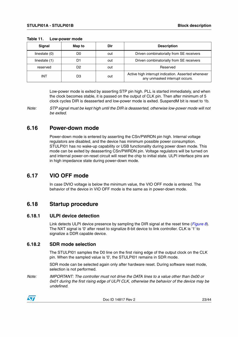
Note: IMPORTANT: The controller must not drive the DATA lines to a value other than 0x00 or 0x01 during the first rising edge of ULPI CLK, otherwise the behavior of the device may be undefined.
Table 11. Low-power mode
Signal Map to Dir Description
linestate (0) D0 out Driven combinatorially from SE receivers
linestate (1) D1 out Driven combinatorially from SE receivers
reserved D2 out Reserved
INT D3 outActive high interrupt indication. Asserted whenever
any unmasked interrupt occurs.

Block description STULPI01A - STULPI01B
24/44 Doc ID 14817 Rev 2
6.18.3 External clock detection
The square wave clock can be applied to the oscillator input. The input square wave clock amplitude is referenced to the DVIO voltage.
The XO pin can be left floating or grounded.
6.18.4 Reset behavior
Typical startup sequence is shown in Figure 12.
STULPI01 contains internal power-on-reset generator which senses the V3V3V and V1V2V voltage. Assertion of RESETn is not necessary for proper initialization. However, if required, this pin can be also used. The internal reset signal is the combination of the signal from RESETn pin and the signal from the internal power-on-reset circuit.
When RESETn is asserted, all internal registers are reset to their default values, the output DIR signal is driven to '1', and data lines pulled low by weak pull-downs.
During reset the STP pin can be driven low, high, or can be left floating. It will be pulled up by internal pull-up and the ULPI interface enters a holding state.
During the reset state the NXT signal is driven low and the CLK is driven high.
When the PLL is stabilized, the clock on the CLK pin is enabled, and DIR is deasserted.
Note: The minimum duration of the external reset signal is TRESETEXT. (See chapter Crystal or external clock detection).
When internal POR reset is asserted, the reset procedure is equivalent to the RESETn signal, with the only exception being that the ULPI lines are in high impedance state. All pull-downs and pull-ups on the ULPI signals are also disabled.
6.18.5 Interface protection
The STULPI01 activates weak pull-downs on data lines and pull-up on the STP during reset and holding state. These are to provide interface protection during startup and anytime the link is not able to drive the ULPI lines properly.
The holding state is entered when the controller drives the STP for more than 1 clock cycle. Any command on the ULPI bus is ignored in this state. For more information, see ULPI specification 1.1, section 3.12 (Safeguarding PHY input signals).
Interface protection can be switched off at any time after startup in order to save power, by writing the Interface Protect Disable bit in the Interface Control register to 1b.
6.18.6 Software reset
The STULPI01 supports software reset by writing the RESET bit in the function control register to 1b.
During the software reset, DIR is asserted and the pull-down resistors on data lines are enabled, but the ULPI registers remain unaffected. Software reset initializes UTMI core logic only. Also, during software reset, external clock detection, SDR mode selection is not performed, and clock is not turned off (PLL is not re-started).
Note: Software reset is not required in the startup procedure for the STULPI. The chip is ready for operation after the hardware reset procedure.
STULPI01A - STULPI01B Block description
Doc ID 14817 Rev 2 25/44
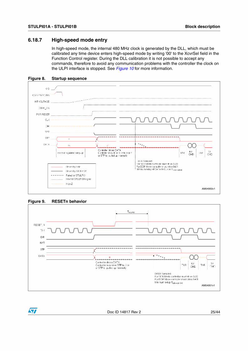
6.18.7 High-speed mode entry
In high-speed mode, the internal 480 MHz clock is generated by the DLL, which must be calibrated any time device enters high-speed mode by writing '00' to the XcvrSel field in the Function Control register. During the DLL calibration it is not possible to accept any commands, therefore to avoid any communication problems with the controller the clock on the ULPI interface is stopped. See Figure 10 for more information.
Figure 8. Startup sequence
Figure 9. RESETn behavior
AM04950v1
AM04951v1

Block description STULPI01A - STULPI01B
26/44 Doc ID 14817 Rev 2
Figure 10. High-speed mode entry
Figure 11. UARTmode entry (2.7 V)
AM04952v1
AM04953v1

STULPI01A - STULPI01B Block description
Doc ID 14817 Rev 2 27/44
Figure 12. UART mode exit (2.7 V)
AM04954v1

State transitions STULPI01A - STULPI01B
28/44 Doc ID 14817 Rev 2
7 State transitions
Table 12. USB state transitions
Signaling mode
Register settings Resistor settings
Xcv
rSel
ect
Term
Sel
ect
Op
Mo
de
Dp
Pu
lldow
n
Dm
Pu
lldow
n
rpu
_dp
_en
rpu
_dm
_en
rpd
_dp
_en
rpd
_dm
_en
hst
erm
_en
General settings
3-state drivers XXb Xb 01b 0b 0b 0b 0b 0b 0b 0b
XXb Xb 01b 1b 1b 0b 0b 1b 1b 0b
Power-up or Vbus < Vth(SESSEND) 01b 0b 00b 1b 1b 0b 0b 1b 1b 0b
Host settings
Host chirp 00b 0b 10b 1b 1b 0b 0b 1b 1b 1b
Host hi-speed 00b 0b 00b 1b 1b 0b 0b 1b 1b 1b
Host full-speed X1b 1b 00b 1b 1b 0b 0b 1b 1b 0b
Host HS/FS suspend 01b 1b 00b 1b 1b 0b 0b 1b 1b 0b
Host HS/FS resume 01b 1b 10b 1b 1b 0b 0b 1b 1b 0b
Host low-speed 10b 1b 00b 1b 1b 0b 0b 1b 1b 0b
Host low-speed suspend 10b 1b 00b 1b 1b 0b 0b 1b 1b 0b
Host low-speed resume 10b 1b 10b 1b 1b 0b 0b 1b 1b 0b
Host test_J/Test_K 00b 0b 10b 1b 1b 0b 0b 1b 1b 1b
Peripheral settings
Peripheral chirp 00b 1b 10b 0b 0b 1b 0b 0b 0b 0b
Peripheral hi-speed 00b 0b 00b 0b 0b 0b 0b 0b 0b 1b
Peripheral full-speed 01b 1b 00b 0b 0b 1b 0b 0b 0b 0b
Peripheral HS/FS suspend 01b 1b 00b 0b 0b 1b 0b 0b 0b 0b
Peripheral HS/FS resume 01b 1b 10b 0b 0b 1b 0b 0b 0b 0b
Peripheral low-speed 10b 1b 00b 0b 0b 0b 1b 0b 0b 0b
Peripheral low-speed suspend 10b 1b 00b 0b 0b 0b 1b 0b 0b 0b
Peripheral low-speed resume 10b 1b 10b 0b 0b 0b 1b 0b 0b 0b

STULPI01A - STULPI01B State transitions
Doc ID 14817 Rev 2 29/44
Peripheral test_J/Test_K 00b 0b 10b 0b 0b 0b 0b 0b 0b 1b
Signaling mode
Register settings Resistor settings
Xcv
rSel
ect
Term
Sel
ect
Op
Mo
de
Dp
Pu
lldow
n
Dm
Pu
lldow
n
rpu
_dp
_en
rpu
_dm
_en
rpd
_dp
_en
rpd
_dm
_en
hst
erm
_en
OTG device, peripheral chirp 00b 1b 10b 0b 1b 1b 0b 0b 1b 0b
OTG device, peripheral hi-speed 00b 0b 00b 0b 1b 0b 0b 0b 1b 1b
OTG device, peripheral full-speed 01b 1b 00b 0b 1b 1b 0b 0b 1b 0b
OTG device, peripheral HS/FS suspend 01b 1b 00b 0b 1b 1b 0b 0b 1b 0b
OTG device peripheral, HS/FS resume 01b 1b 10b 0b 1b 1b 0b 0b 1b 0b
OTG device peripheral, Test_J/Test_K 00b 0b 10b 0b 1b 0b 0b 0b 1b 1b
Table 12. USB state transitions (continued)

ULPI registers STULPI01A - STULPI01B
30/44 Doc ID 14817 Rev 2
8 ULPI registers
Table 13. ULPI register map overview
Field name Size (bits)Address (6 bits)
Rd Wr Set Clr
Immediate register set
Vendor ID low 8 00h - - -
Vendor ID high 8 01h - - -
Product ID low 8 02h - - -
Product ID high 8 03h - - -
Function control 8 04-06h 04h 05h 06h
Interface control 8 07-09h 07h 08h 09h
OTG control 8 0A-0Ch 0Ah 0Bh 0Ch
USB interrupt enable rising 8 0D-0Fh 0Dh 0Eh 0Fh
USB interrupt enable falling 8 10-12h 10h 11h 12h
USB interrupt status register 8 13h - - -
USB interrupt latch register 8 14h - - -
Debug 8 15h - - -
Scratch 8 16-18h 16h 17h 18h
Car kit control register 8 16-1Bh 19h 1Ah 1Bh
Reserved 8 1C-2Eh
Access extended register set (see Table 14) 8 - 2Fh - -
Reserved 8 30-3Ch
Power control 3D-3Fh
Extended register set Address (8 bits)
Maps to immediate register set above 8 00-3Fh
Reserved 8 40-FFh
Table 14. Register access legend
Access code Expanded name Meaning
rd Read Register can be read. Read-only if this is the only mode given.
wr Write Pattern on the data bus will be written over all bits of the register.
s Set Pattern on the data bus is OR’d with and written into the register.
c ClearPattern on the data bus is a mask. If a bit in the mask is set, then the corresponding register bit will be set to zero (cleared).

STULPI01A - STULPI01B ULPI registers
Doc ID 14817 Rev 2 31/44
Table 15. Vendor and product ID
Register Bits Access Address Value Description
VENDOR_ID_LOW 7:0 rd 00h 83 h Lower byte of vendor ID.
VENDOR_ID_HIGH 7:0 rd 01h 04 h Upper byte of vendor ID.
PRODUCT_ID_LOW 7:0 rd 02h 4b h Lower byte of product ID number.
PRODUCT_ID_HIGH 7:0 rd 03h 4f h Upper byte of product ID number.
Table 16. Power control register
(3Dh-3Fh Read, 3Dh Write, 3Eh Set, 3Fh Clear) (Controls various power aspects of the USB trans)
Field name Bits Access Reset Description
Reserved 0 rd/wr/s/c 0b Reserved. The link must never write a 1b to this bit.
Over-current_PD 1 rd/wr/s/c 1bPower control of the internal overcurrent circuit.0b: Enables the overcurrent circuit.1b: Disables the overcurrent circuit.
UART_DIR 2 rd/wr/s/c 0b0b: Txd on DM and Rxd on DP1b: Txd on DP and Rxd on DM
UART_2V7 3 rd/wr/s/c 1b0b: UART signaling at 3V31b: UART signaling at 2V7
Reserved 7:4 rd/wr/s/c 0b Reserved. The link must never write a 1b to these bits.

ULPI registers STULPI01A - STULPI01B
32/44 Doc ID 14817 Rev 2
Table 17. Function control register
04h-06h(Read), 04h(Write), 05h(Set), 06h(Clear) (Controls UTMI function setting of the USB transceiver PHY)
Field name Bits Access Reset Description
XcvrSelect 1:0 rd/wr/s/c 01b
Selects the required transceiver speed.00b: Enable HS transceiver 01b: Enable FS transceiver 10b: Enable LS transceiver 11b: Enable FS transceiver for LS packets (FS preamble is automatically pre-pended)IMPORTANT NOTE: Every time the XcvrSelect is changed to ‘00’, the output ULPI clock is stopped for the time needed for internal DLL calibration.
TermSelect 2 rd/wr/s/c 0b
Controls the internal pull-up resistors or HS terminations. Control over these resistors changes depending on XcvrSelect, OpMode, DpPulldown and DmPulldown, as shown in Table 24.
OpMode 4:3 rd/wr/s/c 00b
Selects the required bit encoding style during transmit. 00b: Normal operation01b: Non-driving 10b: Disables bit-stuff and NRZI encoding 11b: Do not automatically add SYNC and EOP when transmitting. Must be used only for HS packets.
Reset 5 rd/wr/s/c 0b
Active high transceiver reset. After the Link sets this bit, STULPI01 asserts DIR and reset the UTMI+ core. When the reset is completed, STULPI01 de-asserts DIR and automatically clears this bit. After de-asserting DIR, STULPI01 re-asserts DIR and sends an RX CMD update to the Link.Note: If Reset bit is set to ‘1’ and SuspendM bit is set to ‘0’ in the same register access, SuspendM bit takes higher priority and chip will enter low power mode. Reset bit will be cleared.
SuspendM 6 rd/wr/s/c 1b
Active low PHY suspend. Puts PHY into Low Power Mode. STULPI01 automatically sets this bit to ‘1’ when Low-Power Mode is exited.0b: Low-Power Mode 1b: PoweredNote: If Reset bit is set to ‘1’ and SuspendM bit is set to ‘0’ in the same register access, SuspendM bit takes higher priority and chip will enter low power mode. Reset bit will be cleared.
Reserved 7 rd/wr/s/c 0b Reserved
STULPI01A - STULPI01B ULPI registers
Doc ID 14817 Rev 2 33/44
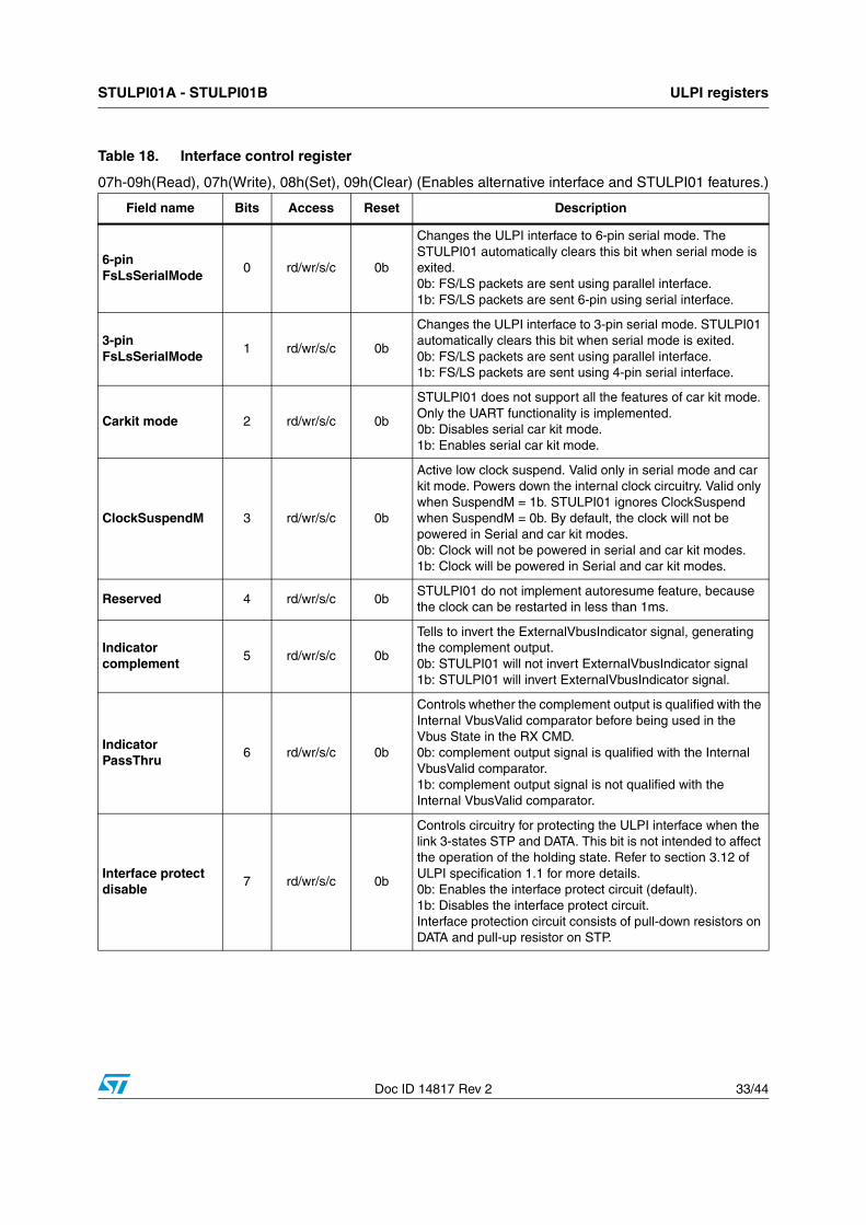
Table 18. Interface control register
07h-09h(Read), 07h(Write), 08h(Set), 09h(Clear) (Enables alternative interface and STULPI01 features.)
Field name Bits Access Reset Description
6-pinFsLsSerialMode
0 rd/wr/s/c 0b
Changes the ULPI interface to 6-pin serial mode. The STULPI01 automatically clears this bit when serial mode is exited.0b: FS/LS packets are sent using parallel interface.1b: FS/LS packets are sent 6-pin using serial interface.
3-pinFsLsSerialMode
1 rd/wr/s/c 0b
Changes the ULPI interface to 3-pin serial mode. STULPI01 automatically clears this bit when serial mode is exited.0b: FS/LS packets are sent using parallel interface.1b: FS/LS packets are sent using 4-pin serial interface.
Carkit mode 2 rd/wr/s/c 0b
STULPI01 does not support all the features of car kit mode. Only the UART functionality is implemented.0b: Disables serial car kit mode.1b: Enables serial car kit mode.
ClockSuspendM 3 rd/wr/s/c 0b
Active low clock suspend. Valid only in serial mode and car kit mode. Powers down the internal clock circuitry. Valid only when SuspendM = 1b. STULPI01 ignores ClockSuspend when SuspendM = 0b. By default, the clock will not be powered in Serial and car kit modes.0b: Clock will not be powered in serial and car kit modes.1b: Clock will be powered in Serial and car kit modes.
Reserved 4 rd/wr/s/c 0bSTULPI01 do not implement autoresume feature, because the clock can be restarted in less than 1ms.
Indicatorcomplement
5 rd/wr/s/c 0b
Tells to invert the ExternalVbusIndicator signal, generating the complement output. 0b: STULPI01 will not invert ExternalVbusIndicator signal1b: STULPI01 will invert ExternalVbusIndicator signal.
Indicator PassThru
6 rd/wr/s/c 0b
Controls whether the complement output is qualified with the Internal VbusValid comparator before being used in the Vbus State in the RX CMD.0b: complement output signal is qualified with the Internal VbusValid comparator.1b: complement output signal is not qualified with the Internal VbusValid comparator.
Interface protect disable
7 rd/wr/s/c 0b
Controls circuitry for protecting the ULPI interface when the link 3-states STP and DATA. This bit is not intended to affect the operation of the holding state. Refer to section 3.12 of ULPI specification 1.1 for more details.0b: Enables the interface protect circuit (default).1b: Disables the interface protect circuit.Interface protection circuit consists of pull-down resistors on DATA and pull-up resistor on STP.

ULPI registers STULPI01A - STULPI01B
34/44 Doc ID 14817 Rev 2
Table 19. OTG control register
0Ah-0Ch(Read), 0Ah(Write), 0Bh(Set), 0Ch(Clear) (Controls UTMI + OTG functions of the PHY)
Field name Bits Access Reset Description
IdPullup 0 rd/wr/s/c 0b
Connects a pull-up to the ID line and enables sampling of the signal level.0b: Disables sampling of ID line.1b: Enables sampling of ID line.
DpPulldown 1 rd/wr/s/c 1bEnables the 15 kOhm pull-down resistor on DP.0b: Pull-down resistor not connected to DP.1b: Pull-down resistor connected to DP.
DmPulldown 2 rd/wr/s/c 1bEnables the 15 kOhm pull-down resistor on DM.0b: Pull-down resistor not connected to DM.1b: Pull-down resistor connected to DM.
DischrgVbus 3 rd/wr/s/c 0b
Discharges VBUS through a resistor. If the link sets this bit to 1, it waits for an RX CMD indicating SessEnd has transition from 0 to 1, and then resets this bit to 0 to stop the discharge.0b: Do not discharge VBUS1b: Discharge VBUS
ChrgVbus 4 rd/wr/s/c 0bCharge VBUS through a resistor. Used for VBUS pulsing SRP. 0b: Do not charge VBUS1b: Charge VBUS
DrvVbus 5 rd/wr/s/c 0b
Signals the internal charge pump or external supply to drive 5V on VBUS.0b: Do not drive VBUS (default)1b: Drive 5V on VBUS
DrvVbus External 6 rd/wr/s/c 0bSelects between the internal and the external 5V VBUS supply. 0b: Drive VBUS using the internal charge pump (default).1b: Drive VBUS using external supply.
UseExternal VbusIndicator
7 rd/wr/s/c 0b
Tells STULPI01 to use an external VBUS over-current indicator. 0b: Use the internal OTG comparator or internalVBUS valid indicator (default)1b: Use external VBUS valid indicator signal

STULPI01A - STULPI01B ULPI registers
Doc ID 14817 Rev 2 35/44
Table 20. USB interrupt enable rising register
0Dh-0Fh(Read), 0Dh(Write), 0Eh(Set), 0Fh(Clear)
(If set, the bits in this register cause an interrupt event notification to be generated when the corresponding PHY signal changes from low to high. By default, all transitions are enabled. RxActive and RxError must always be communicated immediately and so are not included in this register. Interrupt circuitry can be powered down in any mode when both rising and falling edge enables are disabled. To ensure interrupts are detectable when clock is powered down, the link should enable both rising and falling edges.)
Field name Bits Access Reset Description
Host disconnect rise 0 rd/wr/s/c 1b
Generates an interrupt event notification when host disconnect changes from low to high. Applicable only in host mode (DpPulldown and DmPulldown both set to 1b).
VbusValid rise 1 rd/wr/s/c 1bGenerates an interrupt event notification when VbusValid changes from low to high.
SessValid rise 2 rd/wr/s/c 1bGenerate an interrupt event notification when SessValid changes from low to high. SessValid is the same as UTMI+ Avalid.
SessEnd rise 3 rd/wr/s/c 1bGenerates an interrupt event notification when SessEnd changes from low to high.
ID rise 4 rd/wr/s/c 1b
Generates an interrupt event notification when ID changes from low to high. ID is valid 50ms after IdPullup is set to 1b, otherwise ID is undefined and should be ignored.
Reserved 7:5 rd/wr/s/c 0b Reserved.

ULPI registers STULPI01A - STULPI01B
36/44 Doc ID 14817 Rev 2
Table 21. USB interrupt enable falling register
Address: 10h-12h (Read), 10h (Write), 11h (Set), 12h (Clear)
(If set, the bits in this register cause an interrupt event notification to be generated when the corresponding PHY signal changes from high to low. By default, all transitions are enabled. RxActive and RxError must always be communicated immediately and so are not included in this register. Interrupt circuitry can be powered down in any mode when both rising and falling edge enables are disabled. To ensure interrupts are detectable when clock is powered down, the link should enable both rising and falling edges.)
Field name Bits Access Reset Description
Host disconnect fall 0 rd/wr/s/c 1bGenerates an interrupt event notification when the host disconnect changes from high to low. Applicable only in host mode.
VbusValid fall 1 rd/wr/s/c 1bGenerates an interrupt event notification when VbusValid changes from high to low.
SessValid fall 2 rd/wr/s/c 1bGenerates an interrupt event notification when SessValid changes from high to low. SessValid is the same as UTMI+ AValid.
SessEnd fall 3 rd/wr/s/c 1bGenerates an interrupt event notification when SessEnd changes from high to low.
ID fall 4 rd/wr/s/c 1b
Generates an interrupt event notification when ID changes from high to low. ID is valid 50ms after IdPullup is set to 1b, otherwise ID is undefined and should be ignored.
Reserved 7:5 rd/wr/s/c 0b Reserved
Table 22. USB interrupt status register
Address: 13h (Read-only)
(Indicates the current value of the interrupt source signal. Interrupt circuitry can be powered down in any mode when both rising and falling edge enables are disabled. To ensure interrupts are detectable when clock is powered down, the link should enable both rising and falling edges.)
Field name Bits Access Reset Description
Host disconnect 0 rd 0bCurrent value of UTMI+ Host disconnect output. Applicable only in host mode. Automatically reset to 0b when Low-Power Mode is entered.
VbusValid 1 rd 0b Current value of UTMI+VbusValid output.
SessValid 2 rd 0bCurrent value of UTMI+SessValid output. SessValid is the same as UTMI+ AValid.
SessEnd 3 rd 0b Current value of UTMI+SessEnd output.
ID 4 rd 0bCurrent value of UTMI+ID output. ID is valid 50ms after IdPullup is set to 1b, otherwise ID is undefined and should be ignored.
Reserved 7:5 rd 0b Reserved

STULPI01A - STULPI01B ULPI registers
Doc ID 14817 Rev 2 37/44
Table 23. USB interrupt latch register
Address: 14h (Read-only with auto clear)
(These bits are set by the STULPI01 when an unmasked change occurs on the corresponding internal signal. The STULPI01 will automatically clear all bits when the link reads this register, or when low power mode is entered. The STULPI01 also clears this register when serial mode or car kit mode is entered regardless of the value of ClockSuspendM. The interrupt circuitry is powered down in any mode when both rising and falling edge enables are disabled. To ensure the interrupts are detectable when the clock is powered down, the link should enable both rising and falling edges.
The STULPI01 follows the rules in Table 20 for setting any latch register bit. It is important to note that if the register read data is returned to the Link in the same cycle that a USB interrupt latch bit is to be set, the interrupt condition is given immediately in the register read data and the latch bit is not set.
Note that it is optional for the link to read the USB interrupt latch register in synchronous mode because the RX CMD byte already indicates the interrupt source directly.)
Field name Bits Access Reset Description
Host disconnect latch
0 rd 0bSet to 1b by the STULPI01 when an unmasked event occurs on host disconnect. Cleared when this register is read. Applicable only in host mode.
VbusValid latch 1 rd 0bSet to 1b by the STULPI01 when an unmasked event occurs on VbusValid. Cleared when this register is read.
SessValid latch 2 rd 0bSet to 1b by the STULPI01 when an unmasked event occurs on SessValid. Cleared when this register is read. SessValid is the same as UTMI+Avalid.
SessEnd latch 3 rd 0bSet to 1b by the STULPI01 when an unmasked event occurs on SessEnd. Cleared when this register is read.
ID latch 4 rd 0b
Set to 1b by the STULPI01 when an unmasked event occurs on ID. Cleared when this register is read. ID is valid 50ms after ID is set to 1b, otherwise ID is undefined and should be ignored.
Reserved 7:5 rd 0b Reserved
Table 24. Setting rules for interrupt latch register
Input conditions
Resultant value of latch register bitRegister read data returned in current clock cycle
Interrupt latch bit is to be set in current clock cycle
No No 0
No Yes 1
Yes No 0
Yes Yes 0
ULPI registers STULPI01A - STULPI01B
38/44 Doc ID 14817 Rev 2
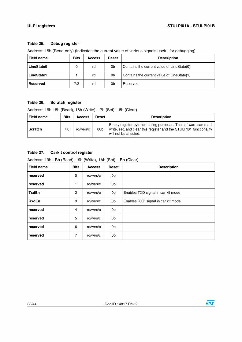
Table 25. Debug register
Address: 15h (Read-only) (Indicates the current value of various signals useful for debugging)
Field name Bits Access Reset Description
LineState0 0 rd 0b Contains the current value of LineState(0)
LineState1 1 rd 0b Contains the current value of LineState(1)
Reserved 7:2 rd 0b Reserved
Table 26. Scratch register
Address: 16h-18h (Read), 16h (Write), 17h (Set), 18h (Clear).
Field name Bits Access Reset Description
Scratch 7:0 rd/wr/s/c 00bEmpty register byte for testing purposes. The software can read, write, set, and clear this register and the STULPI01 functionality will not be affected.
Table 27. Carkit control register
Address: 19h-1Bh (Read), 19h (Write), 1Ah (Set), 1Bh (Clear).
Field name Bits Access Reset Description
reserved 0 rd/wr/s/c 0b
reserved 1 rd/wr/s/c 0b
TxdEn 2 rd/wr/s/c 0b Enables TXD signal in car kit mode
RxdEn 3 rd/wr/s/c 0b Enables RXD signal in car kit mode
reserved 4 rd/wr/s/c 0b
reserved 5 rd/wr/s/c 0b
reserved 6 rd/wr/s/c 0b
reserved 7 rd/wr/s/c 0b

STULPI01A - STULPI01B Package mechanical data
Doc ID 14817 Rev 2 39/44
9 Package mechanical data
In order to meet environmental requirements, ST offers these devices in different grades of ECOPACK® packages, depending on their level of environmental compliance. ECOPACK® specifications, grade definitions and product status are available at: www.st.com. ECOPACK® is an ST trademark.

Package mechanical data STULPI01A - STULPI01B
40/44 Doc ID 14817 Rev 2
Dim.lim.mm s.
Min. Typ. Max. Min. Typ. Max.
A 1.0 1.1 1.16 39.4 43.3 45.7
52.01A 9.8
A2 0.78 0.86 30.7 33.9
b 0.25 0.30 0.35 9.8 11.8 13.8
D 3.5 3.6 3.7 137.8 141.7 145.7
5.21D 98.4
E 3.5 3.6 3.7 137.8 141.7 145.7
5.21E 98.4
15.0e 9.7
7.1255.0F
TFBGA36 mechanical data
7941410/B

STULPI01A - STULPI01B Package mechanical data
Doc ID 14817 Rev 2 41/44
Dim..hcni.mm
Min. Typ. Max. Min. Typ. Max.
A 33 .210 992
C 12.8 13 15.0405.02. 9
7.02.02D 95
.206N 362
765.04.41T
Ao 3.9 0.154
Bo 3.9 0.154
50.005.1oK 9
Po 3.9 161.0451.01.4
P 7. 89 .1 0.3 .011 319
Tape & reel TFBGA36 mechanical data
Note: Drawing not to scale

Order codes STULPI01A - STULPI01B
42/44 Doc ID 14817 Rev 2
10 Order codes
Table 28. Order codes
Order code Key differences Package Packaging
STULPI01ATBR(1)
1. All these versions need digital external clock on XI pin; XO pin must be left floating or grounded (crystal is not supported).
fOSC = 19.2 MHz, CSn/PWRDN = 0 “ON” µTFBGA36 (3.6 x 3.6 mm typ) 3000 parts per reel
STULPI01BTBR(1) fOSC = 26 MHz, CSn/PWRDN = 0 “ON” µTFBGA36 (3.6 x3 .6 mm typ) 3000 parts per reel
STULPI01A - STULPI01B Revision history
Doc ID 14817 Rev 2 43/44
11 Revision history
Table 29. Document revision history
Date Revision Changes
20-Jun-2008 1 First release.
24-Sep-2010 2Replaced “IV8VIO” with “DVIO” throughout datasheet; updated Table 2, 3, 5, 7; updated ECOPACK® text in Section 9; reformatted document, minor textual changes.
STULPI01A - STULPI01B
44/44 Doc ID 14817 Rev 2
Please Read Carefully:
Information in this document is provided solely in connection with ST products. STMicroelectronics NV and its subsidiaries (“ST”) reserve theright to make changes, corrections, modifications or improvements, to this document, and the products and services described herein at anytime, without notice.
All ST products are sold pursuant to ST’s terms and conditions of sale.
Purchasers are solely responsible for the choice, selection and use of the ST products and services described herein, and ST assumes noliability whatsoever relating to the choice, selection or use of the ST products and services described herein.
No license, express or implied, by estoppel or otherwise, to any intellectual property rights is granted under this document. If any part of thisdocument refers to any third party products or services it shall not be deemed a license grant by ST for the use of such third party productsor services, or any intellectual property contained therein or considered as a warranty covering the use in any manner whatsoever of suchthird party products or services or any intellectual property contained therein.
UNLESS OTHERWISE SET FORTH IN ST’S TERMS AND CONDITIONS OF SALE ST DISCLAIMS ANY EXPRESS OR IMPLIEDWARRANTY WITH RESPECT TO THE USE AND/OR SALE OF ST PRODUCTS INCLUDING WITHOUT LIMITATION IMPLIEDWARRANTIES OF MERCHANTABILITY, FITNESS FOR A PARTICULAR PURPOSE (AND THEIR EQUIVALENTS UNDER THE LAWSOF ANY JURISDICTION), OR INFRINGEMENT OF ANY PATENT, COPYRIGHT OR OTHER INTELLECTUAL PROPERTY RIGHT.
UNLESS EXPRESSLY APPROVED IN WRITING BY AN AUTHORIZED ST REPRESENTATIVE, ST PRODUCTS ARE NOTRECOMMENDED, AUTHORIZED OR WARRANTED FOR USE IN MILITARY, AIR CRAFT, SPACE, LIFE SAVING, OR LIFE SUSTAININGAPPLICATIONS, NOR IN PRODUCTS OR SYSTEMS WHERE FAILURE OR MALFUNCTION MAY RESULT IN PERSONAL INJURY,DEATH, OR SEVERE PROPERTY OR ENVIRONMENTAL DAMAGE. ST PRODUCTS WHICH ARE NOT SPECIFIED AS "AUTOMOTIVEGRADE" MAY ONLY BE USED IN AUTOMOTIVE APPLICATIONS AT USER’S OWN RISK.
Resale of ST products with provisions different from the statements and/or technical features set forth in this document shall immediately voidany warranty granted by ST for the ST product or service described herein and shall not create or extend in any manner whatsoever, anyliability of ST.
ST and the ST logo are trademarks or registered trademarks of ST in various countries.
Information in this document supersedes and replaces all information previously supplied.
The ST logo is a registered trademark of STMicroelectronics. All other names are the property of their respective owners.
© 2010 STMicroelectronics - All rights reserved
STMicroelectronics group of companies
Australia - Belgium - Brazil - Canada - China - Czech Republic - Finland - France - Germany - Hong Kong - India - Israel - Italy - Japan - Malaysia - Malta - Morocco - Philippines - Singapore - Spain - Sweden - Switzerland - United Kingdom - United States of America
www.st.com