high-speed vlsi implementation of digit-serial … vlsi implementation of digit-serial gaussian...
TRANSCRIPT

High-speed VLSI implementation of Digit-serial Gaussian
normal basis Multiplication over GF(2m)
Bahram Rashidi1, Sayed Masoud Sayedi2, Reza Rezaeian Farashahi3 1,2Dept. of Elec. & Comp. Eng., Isfahan University of Technology, Isfahan 84156-83111, Iran
3Dept. of Mathematical Sciences, Isfahan University of Technology, Isfahan 84156-83111, Iran 3The School of Mathematics, Institute for Research in Fundamental Sciences (IPM), P.O. Box 19395-5746, Tehran, Iran
[email protected], [email protected], [email protected]
Abstract-- In this paper, by employing the logical effort technique an efficient and high-speed VLSI implementation of
the digit-serial Gaussian normal basis multiplier is presented. It is constructed by using AND, XOR and XOR tree
components. To have a low-cost implementation with low number of transistors, the block of AND gates are
implemented by using NAND gates based on the property of the XOR gates in the XOR tree. To optimally decrease
the delay and increase the drive ability of the circuit the logical effort method as an efficient method for sizing the
transistors is employed. By using this method and also a 4-input XOR gate structure, the circuit is designed for
minimum delay. The digit-serial Gaussian normal basis multiplier is implemented over two binary finite fields
GF(2163) and GF(2233) in 0.18μm CMOS technology for three different digit sizes. The results show that the proposed
structures, compared to previous structures, have been improved in terms of delay and area parameters.
Keywords: Cryptography, Logical Effort, Gaussian Normal Basis multiplication, digit-serial, VLSI implementation
1. Introduction
Several well-known cryptographic algorithms such as Elliptic Curve Cryptography (ECC), Advanced
Encryption Standard (AES), and some message authentication codes are based on the properties of finite fields.
In ECC the use of elliptic curves defined over finite fields is proposed for cryptography schemes, including key
exchange, encryption, and digital signature. A hierarchy process is used for hardware implementation of ECC.
The finite field arithmetic operations such as field multiplication, field squaring, and field inversion are involved
in the implementation process. The most important component in this cryptosystem is field multiplication. The
binary finite fields, denoted by GF(2m), are well suited for hardware implementation, where the addition
operation is performed by modulo 2 without carry bit. The elements in binary fields are represented by a basis.
Two practical bases are polynomial basis (PB) and normal basis (NB). The efficient normal basis for
implementation is denoted by Gaussian normal basis (GNB) [1]. The GNB is considered in several standards
such as IEEE P1363 [2] and NIST [3]. For example, five NIST recommended fields GF(2163), GF(2233),
GF(2283), GF(2409) and GF(2571) are respectively corresponded to the even types 𝑇={4,2,6,4, and 10} of GNB. In
the normal basis representation the powers of two of the field element are implemented only by cyclic shift
operation. In the special case, the squaring operation is performed by only one-bit cyclic shift to left. This
feature can be useful in the hardware implementation of the field multiplier over normal basis.
Many different architectures of the normal basis and GNB multiplications are presented in previous works [4]-
[29]. In [6], a novel scalable multiplication algorithm for a type- 𝑇 Gaussian normal basis by using Hankel
Matrix-Vector representation is presented. In [7] a modified digit-level GNB multiplier over GF(2m) is proposed.
Also for types 𝑇 bigger than 2, a complexity reduction algorithm is proposed to reduce the number of XOR
gates without increasing the gate delay of the digit-level multiplier. In [9] a low-complexity digit-level serial
input parallel output (SIPO) GNB multiplier, also an improved digit-level parallel input serial output (PISO)
multiplier architecture, and a hybrid architecture by connecting the output of the digit-level PISO multiplier to
the input of the digit-level SIPO multiplier are presented. In [10] a new normal basis multiplication algorithm
based on a divide-and-conquer and a uniform shift method is used to implement an efficient multiplexer-based
architecture. A bit-parallel GNB multiplier based on one pipelined XOR tree is designed in [17]. In [21] a novel
algorithm for GNB binary finite field multiplication by using Toeplitz matrix-vector representation is proposed.
Multipliers with systolic and semi-systolic architecture are presented in [5], [14], [16], [18], [19], [20] and [22].
The main problem in the systolic structures is their very high hardware consumption and high numbers of clock
cycles. In [22] the number of clock cycles is reduced.
The focus of this work is on the efficient VLSI implementation of the digit-serial GNB multiplication. Our
previously reported digit-serial Gaussian normal basis multiplier [30] is used for implementation. The multiplier
has a highly regular structure with low critical path delay and low hardware resources, and it is well suited to
hardware implementations. In the multiplier, an XOR tree for summation of partial products exists. A structural
VLSI implementation of the XOR tree based on logical effort technique is presented. In the multiplier structure,
the generated partial products by AND gates blocks are added to each other by XOR tree, because in the binary
field, addition is performed by modulo 2 using XOR gates. Accordingly, the blocks of AND gates are

implemented by NAND gates based on the property of the XOR tree in the multiplier structure. Also, an
optimized 4-input XOR gate is used for implementation of the XOR tree.
The rest of the paper is organized as follows. Section 2 provides a brief background on Gaussian normal basis
multiplication over GF(2m) and the structure of digit-serial GNB multiplier. Section 3 describes the proposed
VLSI implementation of the digit-serial GNB multiplier over GF(2m). Section 4 gives a comparison between this
work and other previously related works. The paper is concluded in section 5.
2. Gaussian normal basis multiplication over GF(2m) and the structure of digit-serial multiplier
Let 𝛽 be a normal element of the binary finite field GF(2m). Then, the set of elements {𝛽, 𝛽2, … , 𝛽2𝑚−1} in
GF(2m) is a basis for the space GF(2m) over GF(2). This means each element 𝐴 ∈GF(2m) can be represented by
𝐴 = ∑ 𝑎𝑖𝛽2𝑖𝑚−1
𝑖=0 = (𝑎0𝛽20+ 𝑎1𝛽21
+ 𝑎2𝛽22+ ⋯ + 𝑎𝑚−2𝛽2𝑚−2
+ 𝑎𝑚−1𝛽2𝑚−1), where 𝑎𝑖 are 0 or 1. And, for
the simplicity, the element 𝐴 is represented by a vector 𝐴 = [𝑎𝑚−1, 𝑎𝑚−2, … , 𝑎2, 𝑎1, 𝑎0]. The addition of two
elements in GF(2m) is computed by bitwise XOR gates. Also the squaring of the element 𝐴 is performed as
follows:
𝐴2 = [𝑎𝑚−2, 𝑎𝑚−3, … , 𝑎0, 𝑎𝑚−1].
One important property of using normal basis representation, as shown in above formula, is performing the
squaring operation very efficiently by a simple one-bit cyclic shift to left. In general case for the positive
integer 𝑛, the computation of 2𝑛-th power of the element 𝐴 is performed via 𝑛-bit cyclic shift to left, i.e.,
𝐴2𝑛= [𝑎𝑚−𝑛−1, 𝑎𝑚−𝑛−2, … , 𝑎1, 𝑎0, 𝑎𝑚−1, … , 𝑎𝑚−𝑛+1, 𝑎𝑚−𝑛].
Also 2−𝑛-th power is computed by 𝑛-bit cyclic shift to right,
𝐴2−𝑛= [𝑎𝑛−1, 𝑎𝑛−2, … , 𝑎1, 𝑎0, 𝑎𝑚−1, 𝑎𝑚−2, … , 𝑎𝑛+1, 𝑎𝑛].
The Gaussian normal basis (GNB) is special class of normal basis for low complexity normal basis [1]-[2]. For
the binary finite field GF(2m), where 𝑚>1 and is not divisible by 8, and for a positive integer 𝑇, let 𝑝 = 𝑚𝑇 + 1
be a prime number such that gcd(𝑚𝑇
𝑘,𝑚) =1, where 𝑘 is the multiplication order of 2 module 𝑝. Then there exists
a normal basis over GF(2m) called the GNB of type 𝑇. In GNB the number of nonzero entries of multiplication
matrix is less or equal to (𝑚𝑇-1). The time and area complexity of the multiplication operation depends on the
type of the normal basis with respect to that basis. In this work, we consider the GNBs with odd values of 𝑚
which are applicable for cryptography applications, and it implies that 𝑇 is an even number.
Here, we briefly discuss the structure of digit-serial Gaussian normal basis multiplier presented in [30]. Let 𝐴, 𝐵
be two elements in GF(2m). The element 𝐵 = [𝑏𝑚−1, 𝑏𝑚−2, … , 𝑏2, 𝑏1, 𝑏0] is divided into 𝑑 words of 𝑤 bits where
𝑑 = ⌈𝑚
𝑤⌉. Then, we have = ∑ 𝐵𝑖
𝑤𝑖=1 , where 𝐵𝑖 = ∑ 𝑏𝑚−(𝑘−1)𝑤−𝑖𝛽
2𝑚−(𝑘−1)𝑤−𝑖𝑑𝑘=1 for 𝑖 = 1, … , 𝑤. Here, we set
𝑏𝑖 = 0 if 𝑖 ≤ 0. The multiplication of elements 𝐴, 𝐵 in GF(2m) is written by
𝐶 = 𝐴𝐵 = 𝐴 ∑ 𝐵𝑖
𝑤
𝑖=1
= ∑ (∑ 𝑏𝑚−(𝑘−1)𝑤−𝑖 𝐴2−(𝑤−𝑖)
𝛽2𝑚−𝑘𝑤
𝑑
𝑘=1
)
2𝑤−𝑖𝑤
𝑖=1
.
In other words, we have
𝐶 = ∑ 𝐶𝑖2𝑤−𝑖
=
𝑤
𝑖=1
((… ((𝐶12 + 𝐶2)
2+ 𝐶3)
2
+ ⋯ )2
+ 𝐶𝑤),
where for 𝑖 = 1, … , 𝑤,
𝐶𝑖 = ∑ 𝑏𝑚−(𝑘−1)𝑤−𝑖 𝐴2−(𝑤−𝑖)𝛽2𝑚−𝑘𝑤
𝑑
𝑘=1
= ∑ 𝑏𝑚−(𝑘−1)𝑤−𝑖 (((𝐴2−(𝑤−1))
2(𝑖−1)
)
2−(𝑚−𝑘𝑤)
𝛽)
2𝑚−𝑘𝑤
.
𝑑
𝑘=1
To have a low-complexity and regular architecture of multiplication by 𝛽2(𝑚−𝑘𝑤), the computation of 𝑥𝛽2(𝑚−𝑘𝑤)
is performed as ((𝑥2−(𝑚−𝑘𝑤)) 𝛽)
2(𝑚−𝑘𝑤)
in three steps; first the exponentiation of the input 𝑥 by 2−(𝑚−𝑘𝑤) is
done, then multiplication by 𝛽 is performed, and finally the exponentiation of the result by 2(𝑚−𝑘𝑤) is
completed. The details of multiplication by 𝛽 which is the main part of the implementation are given in [30]. In
the computation of 𝐶𝑖, the exponentiation by 2−(𝑚−𝑘𝑤) is performed in the following regular form:
((𝐴2−(𝑤−1))
2(𝑖−1)
)
2−(𝑚−𝑘𝑤)
= (… (((𝐴2−(𝑤−1))
2(𝑖−1)
)
2−(𝑚−𝑤)
)
2𝑤
… )
2𝑤
.
In above equation, first exponentiation by 2−(𝑚−𝑤) is computed, and then for 𝑘 = 2,3, … , 𝑑, exponentiations by
2−(𝑚−𝑘𝑤) are generated by a 𝑑-1 length sequence of exponentiation by 2𝑤.
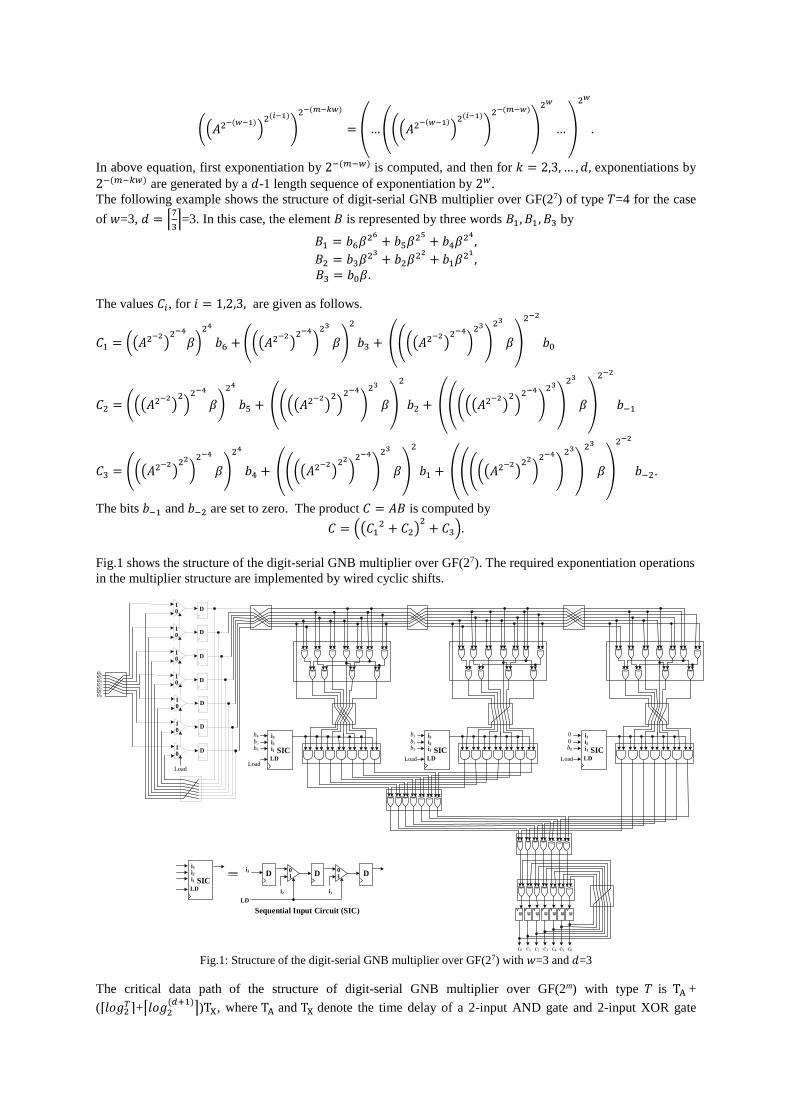
The following example shows the structure of digit-serial GNB multiplier over GF(27) of type 𝑇=4 for the case
of 𝑤=3, 𝑑 = ⌈7
3⌉=3. In this case, the element 𝐵 is represented by three words 𝐵1, 𝐵1 , 𝐵3 by
𝐵1 = 𝑏6𝛽26+ 𝑏5𝛽25
+ 𝑏4𝛽24,
𝐵2 = 𝑏3𝛽23+ 𝑏2𝛽22
+ 𝑏1𝛽21,
𝐵3 = 𝑏0𝛽.
The values 𝐶𝑖, for 𝑖 = 1,2,3, are given as follows.
𝐶1 = ((𝐴2−2)
2−4
𝛽)24
𝑏6 + (((𝐴2−2)
2−4
)23
𝛽)
2
𝑏3 + ((((𝐴2−2)
2−4
)23
)
23
𝛽)
2−2
𝑏0
𝐶2 = (((𝐴2−2)
2)
2−4
𝛽)
24
𝑏5 + ((((𝐴2−2)
2)
2−4
)
23
𝛽)
2
𝑏2 + (((((𝐴2−2)
2)
2−4
)
23
)
23
𝛽)
2−2
𝑏−1
𝐶3 = (((𝐴2−2)
22
)2−4
𝛽)
24
𝑏4 + ((((𝐴2−2)
22
)2−4
)
23
𝛽)
2
𝑏1 + (((((𝐴2−2)
22
)2−4
)
23
)
23
𝛽)
2−2
𝑏−2.
The bits 𝑏−1 and 𝑏−2 are set to zero. The product 𝐶 = 𝐴𝐵 is computed by
𝐶 = ((𝐶12 + 𝐶2)
2+ 𝐶3).
Fig.1 shows the structure of the digit-serial GNB multiplier over GF(27). The required exponentiation operations
in the multiplier structure are implemented by wired cyclic shifts.
10 D
10
D
10 D
10 D
10
D
10
D
10
D b6 SICi1
i2
i3
LD
b5
b4
Load
b3 SICi1
i2
i3
LD
b2
b1
Load
b0 SICi1
i2
i3
LD
00
Load
DDDDDDD
Load
a6a5a4a3a2a1a0
c6c5c4c3c2c1c0
01
i2
i3 01
i1
D
Sequential Input Circuit (SIC)
LD
SICi1
i2
i3
LD
DD
Fig.1: Structure of the digit-serial GNB multiplier over GF(27) with 𝑤=3 and 𝑑=3
The critical data path of the structure of digit-serial GNB multiplier over GF(2m) with type 𝑇 is TA +
(⌈𝑙𝑜𝑔2𝑇⌉+⌈𝑙𝑜𝑔2
(𝑑+1)⌉)TX, where TA and TX denote the time delay of a 2-input AND gate and 2-input XOR gate

respectively [30]. The digit-serial GNB multiplier requires 𝑑𝑚 AND gates and less or equal than 𝑑𝑚+(𝑇-1)(𝑚-
1)𝑑 XOR gates. More details of the hardware and time complexity of this work and other related works are
presented in [30]. In Fig.5, the critical data path is TA +(⌈𝑙𝑜𝑔24⌉+⌈𝑙𝑜𝑔2
(3+1)⌉)TX =TA+5TX . In [30] the output
signal of the multiplier is obtained from flip-flops outputs (see Fig.1 in [30]), so one clock cycle is added to 𝑑
clock cycles and the total number of clock cycles is 𝑑+1. In current work, we change the place of D flip-flops,
and the output signal of multiplier is obtained from final XOR gates outputs in the XOR tree, as seen in Fig.1. In
this case, one clock cycle is reduced and the number of clock cycles is 𝑑. This leads to reduction of clock cycles
by order 𝑂(𝑚) in computation of point multiplication for the elliptic curve cryptography.
3. Proposed Implementation of Digit-serial GNB Multiplier over GF(2m)Based on Logical Effort
The proposed method here is applicable for all multipliers in which an XOR tree is used to perform the sum of
the partial products. The examples are bit-serial ONB multipliers with PISO structure [15], [27], bit-parallel and
digit-serial ONB and GNB multipliers [7]-[14], [28], [30] and bit-parallel and digit-serial PB multipliers [31]-
[34], in the binary finite fields. In these structures to generate partial products, one bit of input operand (for
example 𝐵) is ANDed by an 𝑚-bit vector in the structure of multipliers. In this work, in the structure of digit-
serial GNB multiplier, the number of AND blocks are equal to 𝑑, and each block includes 𝑚 2-input AND
gates. One straightforward method for implementation of AND gate is using NAND-NOT structure, in which in
CMOS structure, any 2-input AND gate is implemented by 6 transistors (4 transistors for NAND gate and 2
transistors for inverter gate). By considering the structure of the multiplier and properties of the XOR gates, the
implementation of the AND gates can be done only by using NAND gates. As seen in the structure of multiplier,
the output of AND blocks in the summation part are bit-wise XORed by XOR tree. We use the following
equation:
𝑎𝑘 ⊕ 𝑎𝑘−1 ⊕ … ⊕ 𝑎1 ⊕ 𝑎0 = �̅�𝑘 ⊕ �̅�𝑘−1 ⊕ … ⊕ �̅�1 ⊕ �̅�0 (1)
which is true if 𝑘 is an even number and 𝑎𝑖 ∈ {0, 1}, for 0 ≤ 𝑖 ≤ 𝑘. Based on this equation XORing of even
numbers of input bits is equal to XORing of the complemented of same input bits. In the case that 𝑘 is an odd
number, since 𝑘-1 is even, based on above equation we have:
𝑎𝑘 ⊕ 𝑎𝑘−1 ⊕ … ⊕ 𝑎1 ⊕ 𝑎0 = 𝑎𝑘 ⊕ �̅�𝑘−1 ⊕ … ⊕ �̅�1 ⊕ �̅�0 (2)
Fig.2 shows configuration of the AND blocks and XOR tree in the multiplier structure. Output signal of register
Reg1 is S and the m-bit output of each AND block is called AP𝑖 where 1 ≤ 𝑖 ≤ 𝑑.
AND-Part
XOR-Tree
mAP1
mAP2
mAP3
mAPd
Input to AND-Part
Output(m-1:0)
S
Reg
1
Fig.2: Configuration of the AND part and XOR tree in the multiplier structure
For each output bit, there are following cases, if 𝑑 is an even number:
Output(𝑗) = AP𝑑(𝑗) ⊕ AP𝑑−1(𝑗) … AP1(𝑗) ⊕ S(𝑗) = AP̅̅̅̅𝑑(𝑗) ⊕ AP̅̅̅̅
𝑑−1(𝑗) ⊕ … ⊕ AP̅̅̅̅1(𝑗) ⊕ S(𝑗) (3)
and if 𝑑 is an odd number we have:
Output(𝑗) = AP𝑑(𝑗) ⊕ AP𝑑−1(𝑗) … AP1(𝑗) ⊕ S(𝑗) = AP̅̅̅̅𝑑(𝑗) ⊕ AP̅̅̅̅
𝑑−1(𝑗) ⊕ … ⊕ AP̅̅̅̅1(𝑗) ⊕ S̅(𝑗)(4)
where Output(𝑗) is 𝑗𝑡ℎ bit of the multiplier output. The schematic of the circuit (for the case of even 𝑑) for one
bit of the multiplier output is shown in Fig.3. Original structure of the AND blocks and XOR tree is shown in

Fig.3 (a). Also Fig.3 (b) shows the implementation of the AND blocks based on the proposed method by NAND
gates.
. . .
. . .
. . .
AP1(j)
S(j)
AP2(j)
AP3(j)
AP4(j)
APd-2(j)
APd-1(j)
APd(j)
Output(j)
Input to AND-Part
. . .
. . .
. . .
AP1(j)
S(j)
AP2(j)
AP3(j)
AP4(j)
APd-2(j)
APd-1(j)
APd(j)
Output(j)
(a) (b)
From SIC Blocks Input to NAND-Part From SIC Blocks
Fig.3: (a) original structure of the AND blocks and XOR tree, (b) and implementation of the AND blocks based on the
proposed method by NAND gates, for 𝑗𝑡ℎ bit of the multiplier output.
In the implementation of the AND blocks by using only NAND gates the number of inverter gates is reduced by
𝑚×𝑑. The proposed approach for implementation of the AND part is applicable for other GNB and polynomial
basis multipliers.
As seen in Fig.1 for generation of partial products in the structure of multiplier, one bit of input operand, for
example 𝑏𝑖, is ANDed by an 𝑚-bit vector. Therefore, one of the input pins of each AND gate must be connected
to 𝑏𝑖 input. Fig.4 (a) shows this concept. Here the 𝑏𝑖 signal must drive 𝑚 NAND gates, since we have changed
the AND gates by NAND gates. If Cin-NAND is the input capacitance of each NAND gate, then 𝑏𝑖 signal has a
capacitance load equal to 𝑚×Cin-NAND. In elliptic curve cryptography, the range of 𝑚 is bigger than 160, so this
capacitance load is very big and it can considerably increase the delay of the circuit. To decrease the delay the 𝑏𝑖
signal is buffered in Fig.4 (b).
In(m-1:0)
bi
m
m
bi
Buffer
(a) (b)
In(m-1:0)
m
m
Fig.4: (a) NAND block, (b) NAND block when 𝑏𝑖 is buffered
Supper buffers are used to drive large capacitance loads for minimum delay. In the following, we discuss the
design of a buffer based on a cascade of N inverters to drive a capacitance load, Cload [35]. Each inverter in the
chain is larger than the previous one by a factor α. Fig.5 (a) shows this structure. The factor α is calculated as
follows:
α=[Cload
C𝑖𝑛1]
1
𝐍 (5)
where C𝑖𝑛1 here is the input capacitance of one NAND gate. For minimum delay the number of inverters N is
calculated by:
N=𝑙𝑛Cload
C𝑖𝑛1 (6)
Equations (5) and (6) are used for the design of the buffer. As an example, the buffer design for field GF(2233) is
presented next . In the proposed structure C𝑖𝑛1=4.263fF and Cload=𝑚×Cin-NAND=233×(3.282fF)=765fF.
N=𝑙𝑛Cload
C𝑖𝑛1= 𝑙𝑛
765
4.263= 5.2~6. So we have 6 inverter stages in the structure of the buffer. The value α is:

α=[Cload
C𝑖𝑛1]
1
𝐍= [
765
4.263]
1
𝟔=2.38
The structure of the buffer that drives one NAND block in the digit-serial GNB multiplier over GF(2233) is
shown in Fig.5 (b).
(Wp1/Wn1) α(Wp1/Wn1) α2(Wp1/Wn1) α
N-1(Wp1/Wn1)
(a)
(b)
(0.44μm
/0.22μm)
2.38(0.44μm
/0.22μm)
2.382(0.44μm
/0.22μm)
2.383(0.44μm
/0.22μm)
2.384(0.44μm
/0.22μm)
2.385(0.44μm
/0.22μm)
Cload
Cload
Fig.5: (a) structure of supper buffer, (b) structure of the buffer for drive of one NAND block over GF(2233)
Another part of the multiplier that needs buffering is the output of D flip-flops connected to 𝛽 blocks. Fig.6
shows the structure after applying the changes for the implementation over GF(27). As seen in the figure, the
digit size 𝑑 is odd, so based on Eq. (4), for implementation of AND blocks by NAND gates the outputs of D
flip-flops (S signals) are inverted.
10 D
10
D
10 D
10 D
10
D
10
D
10
D b6 SICi1
i2
i3
LD
b5
b4
Load
b3 SICi1
i2
i3
LD
b2
b1
Load
b0 SICi1
i2
i3
LD
00
Load
Load
01
i2
i3 01
i1
D
Sequential Input Circuit (SIC)
LD
SICi1
i2
i3
LD
DD
c6c5c4c3c2c1c0
D D D D D D D
a6a5a4a3a2a1a0
Fig.6: Proposed structure for GF(27) after applying changes for VLSI implementation
In Fig.6 the structure of the digit-serial GNB multiplier is constructed by XOR Tree, 𝛽 blocks, NAND gates, D
flip-flops and multiplexers. The main element of the circuit is XOR gate. A brief discussion on different low-
cost full swing circuits of the XOR gates is presented in [36]. In [37] a 6 transistors XOR circuit is designed. In
this circuit, for two states of A=‘1’, B=‘0’ and A=‘0’, B=‘1’ the level of output voltage depends on voltage level
of input signals. In [36], a modified version of XOR gate is presented, in which this limitation is eliminated.
Fig.7 (a) shows the modified 2-input XOR structure in which two minimum size pull-up PMOS transistors are
added to the previous circuit. In this circuit the XOR output (X) and XNOR output (X̅) signals are produced
simultaneously. This is an important property of the structure for construction of the 4-input XOR gate. Fig.7 (b)
shows the implemented layout of the 2-input XOR gate in 0.18μm CMOS technology.

A B
X
(a) (b) Fig.7: (a) 2-input XOR structure in [36], (b) layout of this gate
The 4-input XOR gate is constructed by two modified 2-input XOR gates, pass transistors and one inverter at
the output node [36]. Fig.8 (a) shows the circuit, and the layout of the gate is shown in Fig.8 (b). As seen in the
figure two output signals X and X̅ of the 2-input XOR gates are used for construction of the 4-input XOR gate.
Voltage level and driving capability is restored by using an inverter at the output node.
The effect of process variations and mismatch on the delay of the circuit was evaluated through the Monte Carlo
analysis. Fig.9 shows the result for 500 iterations and for load capacitance of 30fF. As the figure shows the
mean value of the delay is 225.191ps.
(b)(a)
X
A
B
D
C
Fig.8: (a) the structure of the 4-input XOR gate in [36], (b) layout of this gate
Fig.9: Monte Carlo result for the delay of the 4-input XOR circuit
Another component used in the multipliers structure is D flip-flop. Different static flip-flop topologies have
been proposed in the past. Based on a comparative study, some of the widely used topologies have been shown
in Fig.10 (a)-(c). A full characterization of these flip-flops can be found in the literature [38]-[41]. Here, a brief
description of each flip-flop is presented. Fig.10 (a) shows a conventional Transmission Gate Flip-Flop (TGFF).
This structure requires a large number of transistors for implementation. A Push Pull Flip-Flop (PPFF) is shown
in Fig.10 (b) in which an inverter and a transmission gate between the outputs of the master and slave latches

accomplish a push pull effect at the slave latch. Fig.10 (c) shows a Clocked CMOS (C²MOS) flip-flop. In the
figure, the second and fourth C2MOS latches are used to maintain the charge levels at output nodes. These
latches are weak feedback latches with low driving capability. There are 20 transistors used in this circuit, which
is high compared to that of two other circuits.
D Q
clk
clk clk
clk
(a)
clk
clk clk
clk
D Q
clk
clk clk
clk
clk
clk
(b)
clk
clkD
clk
clk
clk
clk
clk
clk
Q
(c) Fig.10: Three different structures of D flip-flop presented in literature.
The Transmission Gate Master-Slave flip-flop (TG-MSFF) [42] shown in Fig.11 (a) is used in current work for
implementation of digit-serial GNB multiplier. In the circuit when the clock signal is high ‘1’, the first
transmission gate in the master part becomes functional samples and transfers input data at node D to the
inverter output node. When the clock goes ‘0’, the second transmission gate in the slave part becomes functional
transfers the data from intermediate inverter output node to the output node Q. This structure is one of the fastest
classical structures [43]. It has a short direct path (low latency direct path) and a low power feedback, which are
constructed by cascading two identical pass gate latches. Based on simulation results presented in [39], [43],
[44], [45], the best power-performance trade-off with total delay (clock-to-output + setup time) is achieved for
this structure. As mentioned before, in this paper, we use this D flip-flop in the proposed implementation of the
digit-serial GNB multiplier. Fig.11 (b) shows the implemented layout of the TG-MSFF in 0.18µm CMOS
technology.
Based on above structures, implementations of the multiplier over two practical fields GF(2163) and GF(2233) for
three digit sizes 𝑑=3, 𝑑=15 and 𝑑=59 are done. In the following, implementations of the GNB multiplier over
field GF(2233) based on logical effort technique is presented. The logical effort technique, describes capability of
one logic gate relative to that of a reference inverter gate [46]. The logical effort of a logic gate is defined as the
ratio of its input capacitance to that of an inverter that delivers equal output current. The logical effort
parameters are presented briefly in [36]. Here, the logical effort is applied to get least overall delay by balancing
the delay among the stages. First implementation of multiplier for (𝑑=59, 𝑤=4) is described. In the general case
as shown in Fig.12 the XOR tree is implemented in six stages by using 2-input XOR gates.
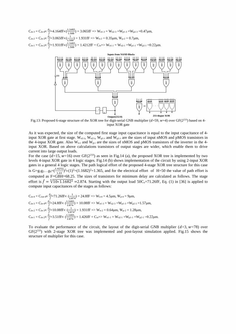
The low-cost 4-input XOR gate with minimum number of transistors is used to implement the XOR tree. The 6-
stage XOR tree in the digit-serial GNB for case (𝑑=59, 𝑤=4) over GF(2233) is implemented by three levels of 4-
input XOR gates. Each 4-input XOR gate constructed by two logic stages including an inverter and a 2-input
XOR gate and pass transistors. The sizes of transistors are computed for different electrical effort by using
logical effort technique. The process for the 6-stage structure of the XOR tree in the digit-serial GNB multiplier
(𝑑=59, 𝑤=4) over GF(2233) which is shown in Fig.13 for H=10 is described in details in the following.

D Q
clk
clkclk
clk
(a)
(b) Fig.11: (a) the structure of the Transmission Gate Master-Slave D flip-flop circuit, (b) the implemented layout of TG-MSFF
Output(232:0)
233
Inputs from AND Blocks
. . .
233-2input XOR
23
3
23
3
23
3
23
3
23
3
23
3
23
3
23
3
23
3
23
3
23
3
23
3
23
3
23
3
23
3
23
3
23
3
23
3
23
3
23
3
23
3
23
3
23
3
23
3
23
3
23
3
23
3
23
3
23
3
23
3
23
3
23
3
23
3
23
3
23
3
23
3
23
3
23
3
23
3
23
3
23
3
23
3
23
3
23
3
23
3
23
3
23
3
23
3
23
3
23
3
23
3
23
3
23
3
23
3
23
3
23
3
23
3
23
3
23
3
23
3
Fig.12: General 6-stage structure of the XOR tree in the digit-serial GNB multiplier (𝑑=59, 𝑤=4) over GF(2233) based on 2-
input XOR gates
For the 6-stage structure, the path logical effort is the product of logical efforts of three inverters and three XOR
gates, calculated as G=g1g2…g6=(1.4252
1.22)3(1)3=(1.1682)3=1.5942. The branching effort is B=1, because there is
no branching along the path; so the path effort is F=GBH=1.594210=15.942. Minimum delay can be realized if
the transistors sizes in each stage are chosen properly. To that end first the stage effort is computed as𝑓 =
√101.168236=1.588. Since H is equal to 10, CL=10Cin= 10Cx=14.252fF where Cx is the input capacitance of
the 4-input XOR gate. The input capacitance of each gate is computed by Eq. (1) in [36]. It can be started with
the load capacitance at the output node of the path. The method is a backward approach as follows:
Cin-6 = Cout-6𝑔6
�̂�=14.252fF(
1
1.588)=8.98fF =>Wn-12=1.62μm, Wp-12 = 3.24μm,
Cin-5 = Cin-6𝑔5
�̂�=8.98fF(
1.1682
1.588) = 6.61fF => Wn1-5 = Wn2-5 =Wp1-5 =Wp2-5 =1μm,
Cin-4 = Cin-5𝑔4
�̂�=6.61fF(
1
1.588) = 4.164fF => Wn-4 = 0.75μm, Wp-4 = 1.5μm,
Cin-3 = Cin-4𝑔3
�̂�=4.164fF(
1.1682
1.588) = 3.065fF => Wn1-3 = Wn2-3 =Wp1-3 =Wp2-3 =0.47μm,
Cin-2 = Cin-3𝑔2
�̂�=3.065fF(
1
1.588) = 1.931fF => Wn-2 = 0.35μm, Wp-2 = 0.7μm,
Cin-1 = Cin-2𝑔1
�̂�=1.931fF(
1.1682
1.588) = 1.4212fF = Cin=> Wn1-1 = Wn2-1 =Wp1-1 =Wp2-1 =0.22μm.
233
233-4input XOR
. . .
Output(232:0)
233
Inputs from NAND Blocks
233
233
233
233
23
3
233
23
3
23
3
233
233
233
233
23
3
233
233
23
3
233
233
233
233
Fig.13: Proposed 6-stage structure of the XOR tree for digit-serial GNB multiplier (𝑑=59, 𝑤=4) over GF(2233) based on 4-
input XOR gate
As it was expected, the size of the computed first stage input capacitance is equal to the input capacitance of 4-
input XOR gate at first stage. Wn1-i, Wn2-i, Wp1-i and Wp1-i are the sizes of input nMOS and pMOS transistors in
the 4-input XOR gate. Also Wn-i and Wp-i are the sizes of nMOS and pMOS transistors of the inverter in the 4-
input XOR. Based on above calculations transistors of output stages are wider, which enable them to drive
current into large output loads.
For the case (𝑑=15, 𝑤=16) over GF(2233) as seen in Fig.14 (a), the proposed XOR tree is implemented by two
levels 4-input XOR gate in 4 logic stages. Fig.14 (b) shows implementation of the circuit by using 2-input XOR
gates in a general 4 logic stages. The path logical effort of the proposed 4-stage XOR tree structure for this case
is G=g1g2…g6=(1.4252
1.22)2(1)2=(1.1682)2=1.365, and for the electrical effort of H=50 the value of path effort is
computed as F=GBH=68.25. The sizes of transistors for minimum delay are calculated as follows. The stage
effort is 𝑓 = √101.168224=2.874. Starting with the output load 50Cx=71.26fF, Eq. (1) in [36] is applied to
compute input capacitances of the stages as follows:
Cin-4 = Cout-4𝑔4
�̂�=71.26fF (
1
2.874) = 24.8fF => Wn-4 = 4.5μm, Wp-4 = 9μm,
Cin-3 = Cin-4𝑔3
�̂�=24.8fF (
1.1682
2.874) = 10.08fF => Wn1-3 = Wn2-3 =Wp1-3 =Wp2-3 =1.57μm,
Cin-2 = Cin-3𝑔2
�̂�=10.08fF (
1
2.874) = 1.931fF => Wn-2 = 0.64μm, Wp-2 = 1.28μm,
Cin-1 = Cin-2𝑔1
�̂�=3.51fF (
1.1682
2.874) = 1.426fF = Cin=> Wn1-1 = Wn2-1 =Wp1-1 =Wp2-1 =0.22μm.
To evaluate the performance of the circuit, the layout of the digit-serial GNB multiplier (𝑑=3, 𝑤=78) over
GF(2233) with 2-stage XOR tree was implemented and post-layout simulation applied. Fig.15 shows the
structure of multiplier for this case.

Output(232:0)
233
Inputs from NAND-Part
Output(232:0)
Inputs from AND-Part
(a) (b)
23
3
23
3
23
3
23
3
23
3
23
3
23
3
23
3
23
3
23
3
23
3
23
3
23
3
23
3
23
3
23
3
23
3
23
3
23
3
23
3
Fig.14: (a) implementation of the XOR tree for digit-serial GNB multiplier (𝑑=15, 𝑤=16) over GF(2233) by the 4-input XOR
gate in 4 logic stages, (b) by using 2-input XOR gates in general 5 logic stages.
In the layout design, proper distribution of the clock signal is an important subject. Here, the main aim in clock
distribution is transmitting the clock signal simultaneously to all D flip-flops. There are different clock
distribution methods such as tree buffer, mesh, H-tree and some combinations of them [47]-[49] that are used to
achieve zero clock skewing. In H-tree clock distribution approach, which is a common zero skew routing
method, by matching the length of each path, from clock source to D flip-flop, zero skew clock routing is
achieved. This is performed by creating a series of routes with “H” shape. At the corners of each “H” the nearly
identical clock signals, provide the inputs to the next level of smaller “H” routes. To minimize reflections, the
impedance of interconnects are scaled. For an H-tree network, each route leaving a junction must have twice the
impedance of the source route. This is accomplished by decreasing the interconnect width of each route. This
continues until the final points of the H-tree structure are used to drive either the D flip-flops, or local buffers
that drive the D flip-flops. In this work, we consider H-tree distribution for clock signal. Fig.16 shows the
topology of clock distribution network based on H-tree method for the proposed structure of the digit-serial
GNB multiplier (𝑑=3, 𝑤=78) over GF(2233).
Output(232:0)
233
233
1
0
Loadβ β β
A(232:0)
b232 SICi1
i2
i78
LD
b231
b155
. .
.
. .
.
b154 SICi1
i2
i78
LD
b153
b77
. .
.
. .
.
b76 SICi1
i2
i78
LD
b75
‘0’
. .
.
. .
.
. . . . . . . . .
Fig.15: Structure of the digit-serial GNB multiplier (𝑑=3, 𝑤=78) over GF(2233) for layout implementation

Mux_DFFs
Beta_NAND-1
SIC-1 & Buffer
Beta_NAND-2
4-input XOR Gates
DFFs & Inverters
Buffers
Beta_NAND-3
SIC-2 & Buffer
SIC-3 & Buffer
CL
K
Fig.16: Topology of clock distribution network based on H-tree in the structure of the digit-serial GNB multiplier (𝑑=3,
𝑤=78) over GF(2233)
The layout of the proposed structure of the digit-serial GNB multiplier (𝑑=3, 𝑤=78) over GF(2233) for the case
of H=10, CL=14.252fF is shown in Fig.17. The area of the layout is 790µm*798µm. Result of Monte Carlo
analysis for the delay of the circuit is shown in Fig.18. The number of iterations is N=300. As the figure shows
the mean value of delay is 580.048ps.
Mux_DFFs, Buffers & Routings
Beta_NAND-1
SIC-1 & Buffer
Beta_NAND-2
SIC-2 & Buffer
Beta_NAND-3
SIC-3 & Buffer
4-input XOR gates & Routings
DFFs, Inverters & Routings
Fig.17: Layout of the proposed structure of the digit-serial GNB multiplier (𝑑=3, 𝑤=78) over GF(2233) for the case of H=10,
CL=14.252fF.

Fig.18: Result of Monte Carlo analysis for the delay of the proposed digit-serial GNB multiplier (𝑑=3, 𝑤=78) over GF(2233)
for the case of H=10, CL=14.252fF and for 300 iterations.
4. Results and Comparison
The proposed structures were successfully implemented in 0.18μm CMOS technology. The parameters of
proposed structures and a comparison between present work and other implementations of the multiplier over
GF(2m) are presented in Tables1 and 2. The comparisons are based on parameters of critical path delay,
calculation time and area. The implementations are presented for different electrical efforts, namely, H=10, 50
and 250. Table 1 shows the results for the proposed implementation of digit-serial GNB multiplier over GF(2163)
and GF(2233) for both cases of applying the logical effort technique and without applying it. Table 2 compares
time and area of the proposed structures and some previously reported structures. The reported simulation
results are based on schematic structures. The areas are estimated by summation of transistors area without
considering the routing and the buffers in clock distribution. Only for the case of 2-stage structure of the digit-
serial GNB multiplier (𝑑=3, 𝑤=78) for H=10 and CL=14.252fF the results are obtained from post layout
simulation. Table 1: Critical path delay, time and area results for the proposed implementation of digit-serial GNB multiplier
Methods Field
CL/ H Critical Path
Delay (ns)
Time (ns) Area(μm2)
6-stage, 𝑑=59 GF(2163) 14.252fF/10 3.268 9.204 2085043
6-stage, 𝑑=59 GF(2163) 71.26fF/50 4.415 12.645 2085043
6-stage, 𝑑=59 GF(2163) 356.3fF/250 6.797 19.791 2085043
5-stage, 𝑑=15 GF(2163) 14.252fF/10 1.843 20.273 564070
5-stage, 𝑑=15 GF(2163) 71.26fF/50 2.916 28.787 564070
5-stage, 𝑑=15 GF(2163) 356.3fF/250 3.520 36.52 564070
6-stage, 𝑑=59 GF(2233) 14.252fF/10 3.011 11.244 1771633
6-stage, 𝑑=59 GF(2233) 71.26fF/50 4.238 16.952 1771633
6-stage, 𝑑=59 GF(2233) 356.3fF/250 6.638 26.148 1771633
5-stage, 𝑑=15 GF(2233) 14.252fF/10 1.510 24.16 498980
5-stage, 𝑑=15 GF(2233) 71.26fF/50 2.584 38.144 498980
5-stage, 𝑑=15 GF(2233) 356.3fF/250 3.347 50.352 498980
2-stage, 𝑑=3 GF(2233) 14.252fF/10 0.850 66.3 160368
Proposed 6-stage with LE, 𝒅=59 GF(2163) 14.252fF/10 1.428 4.284 2060919
Proposed 6-stage with LE, 𝒅=59 GF(2163) 71.26fF/50 1.623 4.869 2064179
Proposed 6-stage with LE, 𝒅=59 GF(2163) 356.3fF/250 2.043 6.129 2088488
Proposed 4-stage with LE, 𝒅=15 GF(2163) 14.252fF/10 1.356 14.916 550867
Proposed 4-stage with LE, 𝒅=15 GF(2163) 71.26fF/50 1.785 19.635 552497
Proposed 4-stage with LE, 𝒅=15 GF(2163) 356.3fF/250 2.231 24.541 571236
Proposed 6-stage with LE, 𝒅=59 GF(2233) 14.252fF/10 1.262 5.048 1737149
Proposed 6-stage with LE, 𝒅=59 GF(2233) 71.26fF/50 1.484 5.936 1741809
Proposed 6-stage with LE, 𝒅=59 GF(2233) 356.3fF/250 2.013 8.052 1775128
Proposed 4-stage with LE, 𝒅=15 GF(2233) 14.252fF/10 1.018 16.288 480107
Proposed 4-stage with LE, 𝒅=15 GF(2233) 71.26fF/50 1.451 23.216 482437
Proposed 4-stage with LE, 𝒅=15 GF(2233) 356.3fF/250 1.880 30.08 503786
Proposed 2-stage with LE,𝒅=3 GF(2233) 14.252fF/10 0.375 29.25 159772
Proposed 2-stage with LE,𝒅=3 1 GF(2233) 14.252fF/10 0.563 43.914 630420 1In this case, results are achieved form post-layout simulation.

Table 2: Comparison of time and area of the proposed structure and other implementations of the multiplier Methods Field Technology CL/ H Time (ns) Area(μm2)
[9] d=11, GNB, DL-SIPO GF(2163) 65nm --- 13.95 34278
[9] d=55, GNB, DL-SIPO GF(2163) 65nm --- 9.75 160298
[9] d=11, GNB, DL-PISO GF(2163) 65nm --- 20.70 34837
[9] d=55, GNB, DL-PISO GF(2163) 65nm --- 10.65 161495
[23] GNB, d=28 GF(2163) 65nm --- 15.2 39091
Proposed 6-stage with LE, 𝒅=59 GF(2163) 180nm 14.252fF/10 4.284 2060919
Proposed 4-stage with LE, 𝒅=15 GF(2163) 180nm 14.252fF/10 14.916 550867
Proposed 6-stage with LE, 𝒅=59 GF(2233) 180nm 14.252fF/10 5.048 1737149
Proposed 4-stage with LE, 𝒅=15 GF(2233) 180nm 14.252fF/10 16.288 480107
Proposed 2-stage with LE, 𝒅=3 GF(2233) 180nm 14.252fF/10 29.25 159772
Proposed 2-stage with LE, 𝒅=3 1 GF(2233) 180nm 14.252fF/10 43.914 630420 1In this case, results are achieved form post-layout simulation.
In [9] and [23] results of time and area are obtained by automatic synthesis tool Design Vision without layout.
As the results show the proposed structures presented in this work when applying the logical effort technique
and the 4-input XOR gate have better results compared to the general structures.
5. Conclusions
An efficient VLSI implementation of the digit-serial Gaussian normal basis multipliers was presented. The
proposed methods are general and applicable for high-speed hardware implementation of the multiplication
operation over binary finite fields. In the proposed structures by using, logical effort technique, 4-input XOR
gate, and implementation of the AND gate blocks by using NAND gates, speed and area of the multiplier over
GF(2163) and GF(2233) have been improved. The proposed implementation is applicable for ASIC
implementation of the elliptic curves cryptosystems.
References
[1] Ash, D.W., Blake, I.F., and Vanstone, S.A., “Low Complexity Normal Bases”, Discrete Applied Math., 25, 1989, pp. 191-210.
[2] IEEE P1363: Editorial Contribution to standard for Public Key Cryptography, 2003. [3] Federal Information Processing Standards Publications (FIPS) 186-2, U.S. Department of Commerce/NIST: Digital Signature
Standard (DSS), 2000.
[4] Horng, J.S., Jou, I.C. and Lee, C.Y., “On complexity of normal basis multiplier using modified Booth’s algorithm”, Proc. of the 7th WSEAS International Conference on Applied Informatics and Communications, Athens, Greece, August 24-26, 2007, pp.12-17.
[5] Chiou, C.W., Chang, H.W., Liang, W.Y., Lee,C.Y., Lin, J.M., Yeh, Y.C., “Low-complexity Gaussian normal basis multiplier over
GF(2m)”, IET Inf. Secur., Vol. 6, No. 4, 2012, pp. 310-317. [6] Lee C.Y., Chiou, C.W., “Scalable Gaussian Normal Basis Multipliers over GF(2m) Using Hankel Matrix-Vector Representation”, J
Sign Process Syst, Vol. 69, No. 2, 2012, pp. 197-211.
[7] Azarderakhsh, R., and Reyhani-Masoleh, A., “A Modified Low Complexity Digit-Level Gaussian Normal Basis Multiplier”, Proc. Third Int’l Workshop Arithmetic of Finite Fields (WAIFI), June 2010, pp. 25-40.
[8] Reyhani-Masoleh, A., “Efficient Algorithms and Architectures for Field Multiplication Using Gaussian Normal Bases”, IEEE Trans.
Computers, Vol. 55, No. 1, Jan. 2006, pp. 34-47. [9] Azarderakhsh, R., and Reyhani-Masoleh, A., “Low-Complexity Multiplier Architectures for Single and Hybrid-Double
Multiplications in Gaussian Normal Bases”, IEEE Trans. Comput., Vol. 62, No. 4, Apr. 2013, pp. 744-757.
[10] Koc C.K. and Sunar, B., “An Efficient Optimal Normal Basis Type II Multiplier over GF(2m)”, IEEE Trans. Computers, Vol. 50, No. 1, Jan. 2001, pp. 83-87.
[11] WunChiou, C., Lin, J.M., Li, Y.K., Lee, C.Y., Chuang, T.P., and Yeh, Y.C., “Pipeline Design of Bit-Parallel Gaussian Normal Basis
Multiplier over GF(2m)”, Advances in Intelligent Systems and Computing, Springer, Vol. 238, 2014, pp. 369-377. [12] Sukcho, Y., Yeon Choi, J., “A new Word-parallel bit-serial Normal basis multiplier over GF(2m)”, International Journal of control
and Automation, Vol. 6, No. 3, June 2013, pp. 209-216.
[13] Horng, J.S., Jou, I.C. and Lee, C.Y., “Low-complexity multiplexer-based normal basis multiplier over GF(2m)”, J Zhejiang Univ Sci, Vol. 10, No.6, 2009, pp. 834-842.
[14] Chuang, T.P., Wun Chiou, C., Lin, S.S., Lee, C.Y., “Fault-tolerant Gaussian normal basis multiplier over GF(2m)”, IET Inf. Secur.,
2012, Vol. 6, No. 3, pp. 157-170.
[15] Reyhani-Masoleh, A., and Hasan, M.A., “Efficient Digit-serial Normal Basis Multipliers over Binary Extension Fields”, ACM
Trans. Embedded Computing Systems, Vol. 3, No. 3, Aug. 2004, pp. 575-592.
[16] Wun Chiou, C., Lee, C.Y., and Yeh, Y.C., “Sequential Type-I Optimal Normal Basis Multiplier and Multiplicative Inverse in GF(2m)”, Tamkang Journal of Science and Engineering, Vol. 13, No. 4, 2010,pp. 423-432.
[17] Reyhani-Masoleh, A. and Hasan, M.A., “Low Complexity Word-Level Sequential Normal Basis Multipliers”, IEEE Trans. Comput.,
Vol. 54, No. 2, Feb. 2005, pp. 98-110. [18] Wang, Z., Wang, X., and Fan, S., “Concurrent Error Detection Architectures for Field Multiplication Using Gaussian Normal
Basis”, Proc. of Information Security, Practice and Experience (ISPEC), LNCS 6047, 2010, pp. 96-109.
[19] Bayat-Sarmadi, S., Hasan, M.A, “Concurrent Error Detection in Finite-Filed Arithmetic Operations Using Pipelined and Systolic Architectures”, IEEE Trans. Comput., Vol. 58, No. 11, 2009, pp. 1553-1567.
[20] Chiou, C.W., Chang, C.C., Lee, C.Y., Lin, J.M., and Hou, T.W., “Concurrent error detection and correction in Gaussian normal
basis multiplier over GF(2m)”, IEEE Trans. Comput., Vol. 58, No. 6, 2009, pp. 851-857. [21] Kwon, S., “A low complexity and a low latency bit parallel systolic multiplier over GF(2m) using an optimal normal basis of type
II”, Proc. of 16th IEEE Symp. Computer Arithmetic, June 2003, pp. 196-202.

[22] Lee, C. and Chang, P., “Digit-Serial Gaussian Normal Basis Multiplier over GF(2m) Using Toeplitz Matrix-Approach”, Proc. Int’l
Conf. Computational Intelligence and Software Eng. (CiSE), 2009, pp. 1-4.
[23] Azarderakhsh, R., Mozaffari Kermani, M., Bayat-Sarmadi, S., and Lee, C.Y., “Systolic Gaussian Normal Basis Multiplier
Architectures Suitable for High-Performance Applications”, IEEE Trans. on Very Large Scale Integration (VLSI) Systems, Vol. 23,
No. 9, 2014, pp.1969-1972. [24] Lee, C.Y., “Concurrent error detection architectures for Gaussian normal basis multiplication over GF(2m)”, Integration, the VLSI
journal, Vol. 43, No. 1, 2010, pp. 113-123.
[25] Wang, Z., Fan, S., “Efficient Montgomery-based semi-systolic multiplier for even-type GNB of GF(2m)”, IEEE Trans. Comput., Vol. 61, No. 3, 2012, pp. 415-419.
[26] Hua Li, Chang Nian Zhang, “Low-Complexity Versatile Finite Field Multiplier in Normal Basis”, EURASIP Journal on Applied
Signal Processing 9, 2002, pp. 954-960. [27] A. Reyhani-Masoleh and M. A. Hasan, “A new construction of Massey-Omura parallel multiplier over GF(2m)” IEEE Trans.
Computers, Vol. 51, 2002, pp. 511-520.
[28] Reyhani-Masoleh, A. and Hasan, M. A., “Low Complexity Word-Level Sequential Normal Basis Multipliers,” IEEE Trans. Computers, Vol. 54, 2005, pp. 98-110.
[29] W. Tang, H. Wu, and M. Ahmadi, “VLSI implementation of bit-parallel word-serial multiplier in GF (2233)”, Proceedings of the 3rd
International EEE-NEWCAS Conference, June 2005, pp. 399-402. [30] Bahram Rashidi, Sayed Masoud Sayedi, Reza Rezaeian Farashahi, “Efficient and Low-complexity Hardware Architecture of
Gaussian Normal Basis Multiplication over GF(2m) for Elliptic Curve Cryptosystems”, IET Circuits Devices Syst., Vol. 10, Iss. 4,
2016, pp. 1-10. [31] Huapeng Wu, “Bit-Parallel Finite Field Multiplier and Squarer Using Polynomial Basis”, IEEE Transactions on Computers, Vol. 51,
No. 7, July 2002, pp. 750-758.
[32] Arash Reyhani-Masoleh, and M. Anwar Hasan, “Low Complexity Bit Parallel Architectures for Polynomial Basis Multiplication over GF(2m)”, IEEE Transactions on Computers, Vol. 53, No. 8, August 2004, pp. 945-959.
[33] Bahram Rashidi, Sayed Masoud Sayedi, Reza Rezaeian Farashahi, “Efficient implementation of bit-parallel fault tolerant polynomial
basis multiplication and squaring over GF(2m)”, IET Comput. Digit. Tech., 2015, pp. 1-12. [34] Bahram Rashidi, Reza Rezaeian Farashahi, Sayed Masoud Sayedi, “Efficient Implementation of Low Time Complexity and Pipelined
Bit-Parallel Polynomial Basis Multiplier over Binary Finite Fields”, the ISC Int'l Journal of Information Security, Vol.7, No.2, 2015, pp. 101-114.
[35] R. Jacob Baker, “CMOS Circuit Design, Layout, and Simulation”, IEEE Press Series on Microelectronic Systems, John Wiley &
Sons, Inc., Hoboken, New Jersey, 3st edn, 2010. [36] Bahram Rashidi, Sayed Masoud Sayedi, Reza Rezaeian Farashahi, “An efficient and high-speed VLSI implementation of optimal
normal basis multiplication over GF(2m) ”, Integration, the VLSI Journal, Vol. 55, 2016, pp. 138-154.
[37] D. Radhakrishanan, “Low-voltage low-power CMOS full adder”, in Proc. of IEE Circuits Devices System, Vol. 148, 2001, pp. 19-24. [38] Saeeid TahmasbiOskuii, “Comparative study on low-power high-performance flip-flops”, Master Thesis, Linköping University, 2003.
[39] Massimo Alioto, Elio Consoli, Gaetano Palumbo, “Flip-Flop Design in Nanometer CMOS”, Springer International Publishing
Switzerland 2015. [40] U. Ko and P.T. Balsara,“High-Performance Energy-Efficient D-Flip-Flop Circuits”, IEEE Transaction on Very Large Scale
Integration (VLSI) Systems, Vol. 8, No. 1, 2000, pp. 94-98.
[41] Imran Ahmed Khan, Mirza Tariq Beg, “A New Area and Power Efficient Single Edge Triggered Flip-Flop Structure for Low Data Activity and High Frequency Applications”, Innovative Systems Design and Engineering, Vol.4, No.1, 2013, pp. 1-12.
[42] G. Gerosa, S. Gary, C. Dietz, D. Pham, K. Hoover, J. Alvarez, H. Sanchez, P. Ippolito, T. Ngo, S. Litch, J. Eno, J. Golab, N.
Vanderschaaf, and J. Kathle, “2.2 W, 80 MHz superscalar RISC processor”, IEEE J. Solid-State Circuits, Vol. 29, Dec. 1994, pp. 1440-1454.
[43] V. Stojanovic and V.G. Oklobdzija, “Comparative Analysis of Master-Slave Latches and Flip-Flops for High-Performance and Low-
Power Systems”, IEEE Journal of Solid-State Circuits, Vol. 34, No. 4, 1999, pp. 536-548. [44] K. Singh, S.C. Tiwari and M. Gupta, “A Master-Slave Flip Flop for Low Voltage Systems with Improved Power-Delay Product”,
World Applied Sciences Journal, Vol. 16, 2012, pp. 45-52.
[45] Veladimir Stojanovic and Vojion G. oklobdzija, “Comparative analysis of Master-Slave latches and flip-flops for high-performance and low-power system”, IEEE Journal of Solid-State circuits, Vol. 34, 1999, pp. 536-548.
[46] Ivan Sutherland and R.F. Sproull, “Logical effort: Designing for speed on the back of an Envelope”, IEEE Advanced Research
in VLSI, MIT Press, March 1991. [47] Hucydides Xanthopoulos, “Clocking in Modern VLSI Systems”, Series on Integrated Circuits and Systems, Springer, 2009.
[48] Eby G. Friedman, “Clock Distribution Networks in Synchronous Digital Integrated Circuits”, Proceedings of the IEEE, Vol. 89, No.
5, May 2001, pp. 665-692. [49] S. Tam, S. Rusu, U. N. Desai, R. Kim, J. Zhang, and I. Young, “Clock Generation and Distribution for the First IA-64
Microprocessor” IEEE J. Solid-State Circuits, Vol. 35, 2000, pp. 1545-1552.