high-voltage adjustable regulator (rev. m)akizukidenshi.com/download/ds/ti/tl783.pdfthe tl783 is an...
TRANSCRIPT

1FEATURES
KTE (PowerFLEX ) PACKAGE(TOP VIEW)
IN
OUT
ADJ
OU
T
KC (TO-220) PACKAGE(TOP VIEW)
OUTIN
ADJOU
T
OU
T
KTT (TO-263) PACKAGE(TOP VIEW)
IN
OUT
ADJ
DESCRIPTION/ORDERING INFORMATION
TL783
www.ti.com ............................................................................................................................................... SLVS036M–SEPTEMBER 1981–REVISED APRIL 2008
HIGH-VOLTAGE ADJUSTABLE REGULATOR
2• Output Adjustable From 1.25 V to 125 V When Thermal-Shutdown ProtectionUsed With an External Resistor Divider • 0.001%/V Typical Input Voltage Regulation
• 700-mA Output Current • 0.15% Typical Output Voltage Regulation• Full Short-Circuit, Safe-Operating-Area, and • 76-dB Typical Ripple Rejection
The TL783 is an adjustable three-terminal high-voltage regulator with an output range of 1.25 V to 125 V and aDMOS output transistor capable of sourcing more than 700 mA. It is designed for use in high-voltage applicationswhere standard bipolar regulators cannot be used. Excellent performance specifications, superior to those ofmost bipolar regulators, are achieved through circuit design and advanced layout techniques.
As a state-of-the-art regulator, the TL783 combines standard bipolar circuitry with high-voltage double-diffusedMOS transistors on one chip, to yield a device capable of withstanding voltages far higher than standard bipolarintegrated circuits. Because of its lack of secondary-breakdown and thermal-runaway characteristics usuallyassociated with bipolar outputs, the TL783 maintains full overload protection while operating at up to 125 V frominput to output. Other features of the device include current limiting, safe-operating-area (SOA) protection, andthermal shutdown. Even if ADJ is disconnected inadvertently, the protection circuitry remains functional.
Only two external resistors are required to program the output voltage. An input bypass capacitor is necessaryonly when the regulator is situated far from the input filter. An output capacitor, although not required, improvestransient response and protection from instantaneous output short circuits. Excellent ripple rejection can beachieved without a bypass capacitor at the adjustment terminal.
ORDERING INFORMATION (1)
TJ PACKAGE (2) ORDERABLE PART NUMBER TOP-SIDE MARKINGPowerFLEX™ – KTE Reel of 2000 TL783CKTER TL783
0°C to 125°C TO-263 – KTT Reel of 500 TL783CKTTR TL783CTO-220 – KC Tube of 50 TL783CKC TL783C
(1) For the most current package and ordering information, see the Package Option Addendum at the end of this document, or see the TIweb site at www.ti.com.
(2) Package drawings, thermal data, and symbolization are available at www.ti.com/packaging.
1
Please be aware that an important notice concerning availability, standard warranty, and use in critical applications ofTexas Instruments semiconductor products and disclaimers thereto appears at the end of this data sheet.
2PowerFLEX, PowerPAD are trademarks of Texas Instruments.
PRODUCTION DATA information is current as of publication date. Copyright © 1981–2008, Texas Instruments IncorporatedProducts conform to specifications per the terms of the TexasInstruments standard warranty. Production processing does notnecessarily include testing of all parameters.
参考資料

+
−
ProtectionCircuit
OUT
IN
VrefR1
R2
VO
VI
ErrorAmplifier
ADJ
VO Vref1 R2R1
Absolute Maximum Ratings (1)
Package Thermal Data (1)
Recommended Operating Conditions
TL783
SLVS036M–SEPTEMBER 1981–REVISED APRIL 2008 ............................................................................................................................................... www.ti.com
FUNCTIONAL BLOCK DIAGRAM
over operating temperature range (unless otherwise noted)
MIN MAX UNITVl – VO Input-to-output differential voltage 125 VTJ Operating virtual junction temperature 150 °CTstg Storage temperature range –65 150 °C
(1) Stresses beyond those listed under "absolute maximum ratings" may cause permanent damage to the device. These are stress ratingsonly, and functional operation of the device at these or any other conditions beyond those indicated under "recommended operatingconditions" is not implied. Exposure to absolute-maximum-rated conditions for extended periods may affect device reliability.
PACKAGE BOARD θJC θJP(2) θJA
PowerFLEX (KTE) High K, JESD 51-5 2.7°C/W 23°C/WTO-263 (KTT) High K, JESD 51-5 18°C/W 1.94°C/W 25.3°C/WTO-220 (KC) High K, JESD 51-5 17°C/W 3°C/W 19°C/W
(1) Maximum power dissipation is a function of TJ(max), θJA, and TA. The maximum allowable power dissipation at any allowable ambienttemperature is PD = (TJ(max) – TA)/θJA. Operating at the absolute maximum TJ of 150°C can affect reliability. Due to variations inindividual device electrical characteristics and thermal resistance, the built-in thermal overload protection may be activated at powerlevels slightly above or below the rated dissipation.
(2) For packages with exposed thermal pads, such as QFN, PowerPAD™, or PowerFLEX, θJP is defined as the thermal resistance betweenthe die junction and the bottom of the exposed pad.
MIN MAX UNITVl – VO Input-to-output differential voltage 125 VIO Output current 15 700 mATJ Operating virtual junction temperature 0 125 °C
2 Submit Documentation Feedback Copyright © 1981–2008, Texas Instruments Incorporated
Product Folder Link(s): TL783
参考資料

Electrical Characteristics
TL783
www.ti.com ............................................................................................................................................... SLVS036M–SEPTEMBER 1981–REVISED APRIL 2008
Vl – VO = 25 V, IO = 0.5 A, TJ = 0°C to 125°C (unless otherwise noted)
PARAMETER TEST CONDITIONS (1) MIN TYP MAX UNITTJ = 25°C 0.001 0.01Vl – VO = 20 V to 125 V,Input voltage regulation (2) %/VP ≤ rated dissipation TJ = 0°C to 125°C 0.004 0.02
Ripple rejection ΔVI(PP) = 10 V, VO = 10 V, f = 120 Hz 66 76 dBVO ≤ 5 V 7.5 25 mVIO = 15 mA to 700 mA,
TJ = 25°C VO ≥ 5 V 0.15 0.5 %Output voltage regulation
VO ≤ 5 V 20 70 mVIO = 15 mA to 700 mA,P ≤ rated dissipation VO ≥ 5 V 0.3 1.5 %
Output voltage change with temperature 0.4 %Output voltage long-term drift 1000 hours at TJ = 125°C, Vl – VO = 125 V 0.2 %Output noise voltage f = 10 Hz to 10 kHz, TJ = 25°C 0.003 %Minimum output current to maintain regulation Vl – VO = 125 V 15 mA
Vl – VO = 25 V, t = 1 ms 1100Vl – VO = 15 V, t = 30 ms 715
Peak output current mAVl – VO = 25 V, t = 30 ms 700 900Vl – VO = 125 V, t = 30 ms 100 250
ADJ input current 83 110 µAVl – VO = 15 V to 125 V, IO = 15 mA to 700 mA,Change in ADJ input current 0.5 5 µAP ≤ rated dissipationVl – VO = 10 V to 125 V, IO = 15 mA to 700 mA,Reference voltage (OUT to ADJ) (3) 1.2 1.27 1.3 VP ≤ rated dissipation
(1) Pulse-testing techniques maintain the junction temperature as close to the ambient temperature as possible. Thermal effects must betaken into account separately.
(2) Input voltage regulation is expressed here as the percentage change in output voltage per 1-V change at the input(3) Due to the dropout voltage and output current-limiting characteristics of this device, output current is limited to less than 700 mA at
input-to-output voltage differentials of less than 25 V.
Copyright © 1981–2008, Texas Instruments Incorporated Submit Documentation Feedback 3
Product Folder Link(s): TL783
参考資料

TYPICAL CHARACTERISTICS
2
1.8
1.6
1.4
1.2
1
0.8
0.6
0.4
0.2
0250 50 75 100 125
Out
put C
urre
nt L
imit
− A
VI − VO − Input-to-Output V oltage Differential − V
ÎÎÎÎÎÎÎÎÎÎÎÎÎÎÎÎtw = 1 ms ÎÎÎÎÎÎÎÎÎÎÎÎTJ = 0°CÎÎÎÎÎÎÎÎÎÎÎÎÎÎÎÎTJ = 25°CÎÎÎÎÎÎÎÎÎÎÎÎTJ = 125°C0.2
0.4
0.6
0.8
1
1.2
1.4
1.6
1.8
2
00 25 50 75 100
Out
put C
urre
nt L
imit
− A
VI − VO − Input-to-Output V oltage Differential − V
ÎÎÎÎÎÎÎÎÎÎÎÎÎÎÎÎtw = 30 ms ÎÎÎÎÎÎÎÎÎÎÎÎÎÎÎÎTJ = 0°CÎÎÎÎÎÎÎÎÎÎÎÎTJ = 25°CÎÎÎÎÎÎÎÎÎÎÎÎTJ = 125°C
125
0 10 20 30 40
1.6
1.4
1.2
1
0.8
0.6
0.4
0.2
0
Out
put C
urre
nt L
imit
− A
Time − ms
ÎÎÎÎÎÎÎÎÎÎÎÎÎÎÎÎÎÎÎÎVI − VO = 25 VTJ = 25°C
0 10 20 30 40 50 60 70 80 90
100
80
60
40
20
0
120
Rip
ple
Rej
ectio
n −
dB
VO − Output V oltage − V
ÎÎÎÎÎÎÎÎÎÎÎÎÎÎÎÎÎÎÎÎÎÎÎÎÎÎÎÎÎÎÎÎÎÎÎÎÎÎÎÎÎÎVI(AV) − VO = 25 V∆VI(PP) = 10 VIO = 100 mAf = 120 HzCo = 0TJ = 25°C
100
TL783
SLVS036M–SEPTEMBER 1981–REVISED APRIL 2008 ............................................................................................................................................... www.ti.com
OUTPUT CURRENT LIMIT OUTPUT CURRENT LIMITvs vs
INPUT-TO-OUTPUT VOLTAGE DIFFERENTIAL INPUT-TO-OUTPUT VOLTAGE DIFFERENTIAL
Figure 1. Figure 2.
OUTPUT CURRENT LIMIT RIPPLE REJECTIONvs vs
TIME OUTPUT VOLTAGE
Figure 3. Figure 4.
4 Submit Documentation Feedback Copyright © 1981–2008, Texas Instruments Incorporated
Product Folder Link(s): TL783
参考資料

0 100 200 300 400 500 600 700 800
Rip
ple
Rej
ectio
n −
dB
IO − Output Current − mA
100
80
60
40
20
0
ÎÎÎÎÎÎÎÎÎÎÎÎÎÎÎÎÎÎÎÎÎÎÎÎÎÎÎÎÎÎÎÎÎÎÎVI(AV) = 25 V∆VI(PP) = 10 VVO = 10 Vf = 120 HzCo = 0TJ = 25°C
100
0.01
90
80
70
60
50
40
30
20
10
00.1 1 10 100 1000
ÎÎÎÎÎÎÎÎÎÎÎÎÎÎÎÎCo = 10 µF
Rip
ple
Rej
ectio
n −
dB
f − Frequency − kHz
ÎÎÎÎÎÎÎÎÎÎÎÎCo = 0
ÎÎÎÎÎÎÎÎÎÎÎÎÎÎÎÎÎÎÎÎÎÎÎÎÎÎÎÎÎÎVI(AV) = 25 V∆VI(PP) = 10 VVO = 10 VIO = 500 mATJ = 25°C
1.30
1.29
1.28
1.27
1.26
1.25
1.24
1.23
1.22−75 −50 −25 0 25 50 75 100 125 150
− R
efer
ence
Vol
tage
− V
TJ − Virtual Junction T emperature − °C
ÎÎÎÎÎÎÎÎÎÎÎÎÎÎÎÎVI = 20 VIO = 15 mA
Vre
f
175
1
f − Frequency − kHz
ÎÎÎÎÎÎÎÎÎÎÎÎÎÎÎÎÎÎÎÎVI = 35 VVO = 10 VIO = 500 mATJ = 25°C
101 102 103 104 105 106 107
10−1
10−2
10−3
10−4
101
102
− O
utpu
t Im
peda
nce
−Ω
Zo
TL783
www.ti.com ............................................................................................................................................... SLVS036M–SEPTEMBER 1981–REVISED APRIL 2008
TYPICAL CHARACTERISTICS (continued)
RIPPLE REJECTION RIPPLE REJECTIONvs vs
OUTPUT CURRENT FREQUENCY
Figure 5. Figure 6.
OUTPUT IMPEDANCE REFERENCE VOLTAGEvs vs
FREQUENCY VIRTUAL JUNCTION TEMPERATURE
Figure 7. Figure 8.
Copyright © 1981–2008, Texas Instruments Incorporated Submit Documentation Feedback 5
Product Folder Link(s): TL783
参考資料

86
84
82
800 25 50 75
88
90
100 125
TJ − Virtual Junction T emperature − °C
VI = 25 VVO = VrefIO = 500 mA
AD
J In
put C
urre
nt −
µA
20
10
5
0−75 −50 −25 0 25 50
Dro
pout
Vol
tage
− V
75 100 125
25
15
TJ − Virtual Junction T emperature − °C
∆VO = 100 mV
IO = 700 mAIO = 600 mAIO = 500 mA
IO = 250 mA
IO = 100 mAIO = 15 mA
6
4
2
00 25 50 75
− O
utpu
t Cur
rent
− m
A 8
10
12
100 125
I O
VI − Input V oltage − V
TJ = 25°C
TJ = 125°C
TJ = 0°C
−0.2
−0.3
−0.4
−0.50 25 50 75 100 125 150
− O
utpu
t Vol
tage
Dev
iatio
n −
% −0.1
0
∆VO
TJ − Virtual Junction T emperature − °C
VI = 25 VVO = 5 VIO = 15 mA to 700 mA
TL783
SLVS036M–SEPTEMBER 1981–REVISED APRIL 2008 ............................................................................................................................................... www.ti.com
TYPICAL CHARACTERISTICS (continued)
INPUT CURRENT AT ADJ DROPOUT VOLTAGEvs vs
VIRTUAL JUNCTION TEMPERATURE VIRTUAL JUNCTION TEMPERATURE
Figure 9. Figure 10.
OUTPUT VOLTAGE DEVIATION OUTPUT CURRENT(1)
vs vsVIRTUAL JUNCTION TEMPERATURE INPUT VOLTAGE
Figure 11. (1) This is the minimum current required tomaintain voltage regulation.
Figure 12.
6 Submit Documentation Feedback Copyright © 1981–2008, Texas Instruments Incorporated
Product Folder Link(s): TL783
参考資料
VI = 35 VVO = 10 VCo = 1 µFTJ = 25°C
− O
utpu
t Cur
rent
−
AI O
6
4
2
0
−2
−4
−6
0.8
0.6
0.4
0.2
00 40 80 120 160 200 240
Time − µs
− O
utpu
t Vol
tage
Dev
iatio
n −
VV
O∆
ÎÎÎÎÎÎÎÎÎÎÎÎÎÎÎÎTJ = 25°CÎÎÎÎÎÎÎÎÎCo = 0ÎÎÎÎÎÎÎÎÎÎÎÎÎÎÎCo = 10 µF
0 1 2 3 4
Time − µs
− O
utpu
t Vol
tage
Dev
iatio
n −
VV
OC
hang
e in
Inpu
t Vol
tage
− V
0.4
0.2
0
−0.2
1
0.5
0
∆
TL783
www.ti.com ............................................................................................................................................... SLVS036M–SEPTEMBER 1981–REVISED APRIL 2008
TYPICAL CHARACTERISTICS (continued)
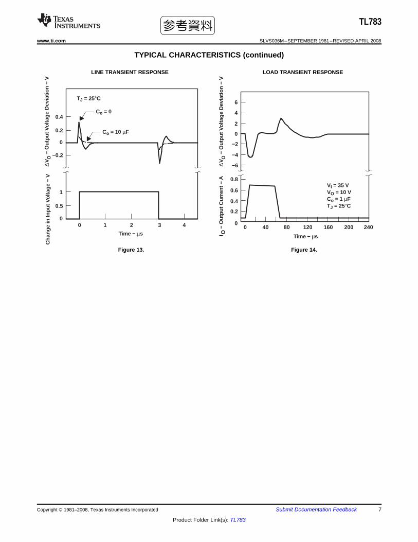
LINE TRANSIENT RESPONSE LOAD TRANSIENT RESPONSE
Figure 13. Figure 14.
Copyright © 1981–2008, Texas Instruments Incorporated Submit Documentation Feedback 7
Product Folder Link(s): TL783
参考資料

DESIGN CONSIDERATIONS
Bypass Capacitors
Protection Circuitry
TL783
SLVS036M–SEPTEMBER 1981–REVISED APRIL 2008 ............................................................................................................................................... www.ti.com
The internal reference (see functional block diagram) generates 1.25 V nominal (Vref) between OUT and ADJ.This voltage is developed across R1 and causes a constant current to flow through R1 and the programmingresistor R2, giving an output voltage of:
VO = Vref (1 + R2/R1) + lI(ADJ) (R2)
orVO ≈ Vref (1 + R2/R1)
The TL783 was designed to minimize the input current at ADJ and maintain consistency over line and loadvariations, thereby minimizing the associated (R2) error term.
To maintain II(ADJ) at a low level, all quiescent operating current is returned to the output terminal. This quiescentcurrent must be sunk by the external load and is the minimum load current necessary to prevent the output fromrising. The recommended R1 value of 82 Ω provides a minimum load current of 15 mA. Larger values can beused when the input-to-output differential voltage is less than 125 V (see the output-current curve in Figure 12) orwhen the load sinks some portion of the minimum current.
The TL783 regulator is stable without bypass capacitors; however, any regulator becomes unstable with certainvalues of output capacitance if an input capacitor is not used. Therefore, the use of input bypassing isrecommended whenever the regulator is located more than four inches from the power-supply filter capacitor. A1-µF tantalum or aluminum electrolytic capacitor usually is sufficient.
Adjustment-terminal capacitors are not recommended for use on the TL783 because they can seriously degradeload transient response, as well as create a need for extra protection circuitry. Excellent ripple rejection presentlyis achieved without this added capacitor.
Due to the relatively low gain of the MOS output stage, output voltage dropout may occur under large-loadtransient conditions. The addition of an output bypass capacitor greatly enhances load transient response andprevents dropout. For most applications, it is recommended that an output bypass capacitor be used, with aminimum value of:
Co (µF) = 15/VO
Larger values provide proportionally better transient-response characteristics.
The TL783 regulator includes built-in protection circuits capable of guarding the device against most overloadconditions encountered in normal operation. These protective features are current limiting, safe-operating-areaprotection, and thermal shutdown. These circuits protect the device under occasional fault conditions only.Continuous operation in the current limit or thermal shutdown mode is not recommended.
The internal protection circuits of the TL783 protect the device up to maximum-rated VI as long as certainprecautions are taken. If Vl is switched on instantaneously, transients exceeding maximum input ratings mayoccur, which can destroy the regulator. Usually, these are caused by lead inductance and bypass capacitorscausing a ringing voltage on the input. In addition, when rise times in excess of 10 V/ns are applied to the input,a parasitic npn transistor in parallel with the DMOS output can be turned on, causing the device to fail. If thedevice is operated over 50 V and the input is switched on, rather than ramped on, a low-Q capacitor, such astantalum or aluminum electrolytic, should be used, rather than ceramic, paper, or plastic bypass capacitors. A Qfactor of 0.015, or greater, usually provides adequate damping to suppress ringing. Normally, no problems occurif the input voltage is allowed to ramp upward through the action of an ac line rectifier and filter network.
Similarly, when an instantaneous short circuit is applied to the output, both ringing and excessive fall times canresult. A tantalum or aluminum electrolytic bypass capacitor is recommended to eliminate this problem. However,if a large output capacitor is used, and the input is shorted, addition of a protection diode may be necessary toprevent capacitor discharge through the regulator. The amount of discharge current delivered is dependent onoutput voltage, size of capacitor, and fall time of Vl. A protective diode (see Figure 15) is required only forcapacitance values greater than:
Co (µF) = 3 × 10⁴/(VO)2
8 Submit Documentation Feedback Copyright © 1981–2008, Texas Instruments Incorporated
Product Folder Link(s): TL783
参考資料

IN
TL783
OUT VO
R1
R2
ADJ
VI
Co
Load Regulation
VI
TL783
R1
Rline
RL
R2
VO
IN OUT
ADJ
TL783
www.ti.com ............................................................................................................................................... SLVS036M–SEPTEMBER 1981–REVISED APRIL 2008
Care always should be taken to prevent insertion of regulators into a socket with power on. Power should beturned off before removing or inserting regulators.
Figure 15. Regulator With Protective Diode
The current-set resistor (R1) should be located close to the regulator output terminal, rather than near the load.This eliminates long line drops from being amplified, through the action of R1 and R2, to degrade load regulation.To provide remote ground sensing, R2 should be near the load ground.
Figure 16. Regulator With Current-Set Resistor
Copyright © 1981–2008, Texas Instruments Incorporated Submit Documentation Feedback 9
Product Folder Link(s): TL783
参考資料
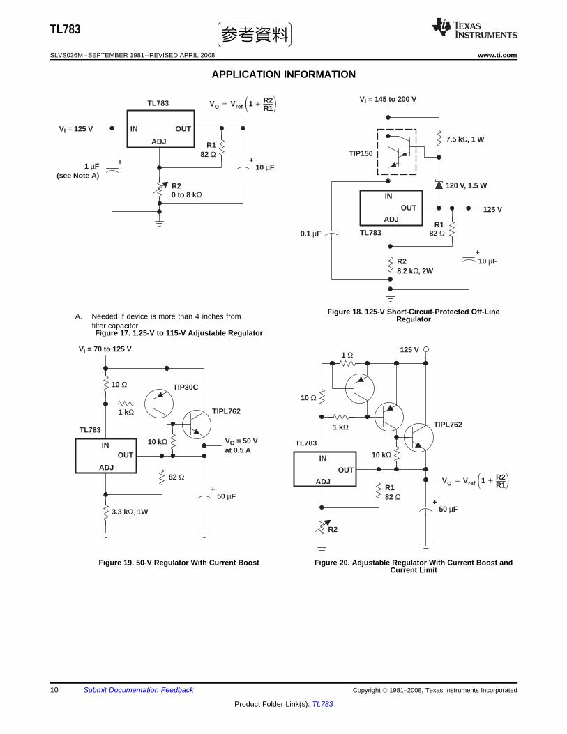
APPLICATION INFORMATION
VI = 125 V
TL783
IN OUT
ADJ
1 µF(see Note A)
0 to 8 kΩ
10 µF
R2
R182 Ω
++
VO Vref 1 R2R1
10 µF
0.1 µF
IN
OUT
ADJ
R28.2 kΩ, 2W
125 V
120 V, 1.5 W
7.5 kΩ, 1 W
VI = 145 to 200 V
TIP150
TL783R1
82 Ω
+
50 µF
82 Ω+
VI = 70 to 125 V
10 Ω
1 kΩ
TIP30C
TIPL762
VO = 50 Vat 0.5 A
TL783
3.3 kΩ, 1W
10 kΩINOUT
ADJ
50 µF+
125 V
10 Ω
1 kΩ TIPL762
1 Ω
R2
TL783
R182 Ω
10 kΩIN
OUT
ADJ VO Vref 1 R2R1
TL783
SLVS036M–SEPTEMBER 1981–REVISED APRIL 2008 ............................................................................................................................................... www.ti.com
Figure 18. 125-V Short-Circuit-Protected Off-LineA. Needed if device is more than 4 inches from Regulatorfilter capacitorFigure 17. 1.25-V to 115-V Adjustable Regulator
Figure 19. 50-V Regulator With Current Boost Figure 20. Adjustable Regulator With Current Boost andCurrent Limit
10 Submit Documentation Feedback Copyright © 1981–2008, Texas Instruments Incorporated
Product Folder Link(s): TL783
参考資料

VI
Load
R
IVrefR
IN
OUT
ADJ
TL783
VI
1 µF
R
TL783
Load
IN
OUT
ADJ
IVrefR
6.25 Ω
48 V
82 Ω
3.9 kΩ
VI = 90 V
TL783
TL783
INOUT
ADJ
IN
OUT
ADJV +
INPUT
V −
TL081
R2
OUTPUT
VCC
1 µF
−
+
TL783
82 Ω
VOFFSET Vref I R282
IN
OUT
ADJ
TL783
www.ti.com ............................................................................................................................................... SLVS036M–SEPTEMBER 1981–REVISED APRIL 2008
Figure 21. Current-Sinking Regulator Figure 22. Current-Sourcing Regulator
Figure 23. High-Voltage Unity-Gain Offset Amplifier Figure 24. 48-V 200-mA Float Charger
Copyright © 1981–2008, Texas Instruments Incorporated Submit Documentation Feedback 11
Product Folder Link(s): TL783
参考資料
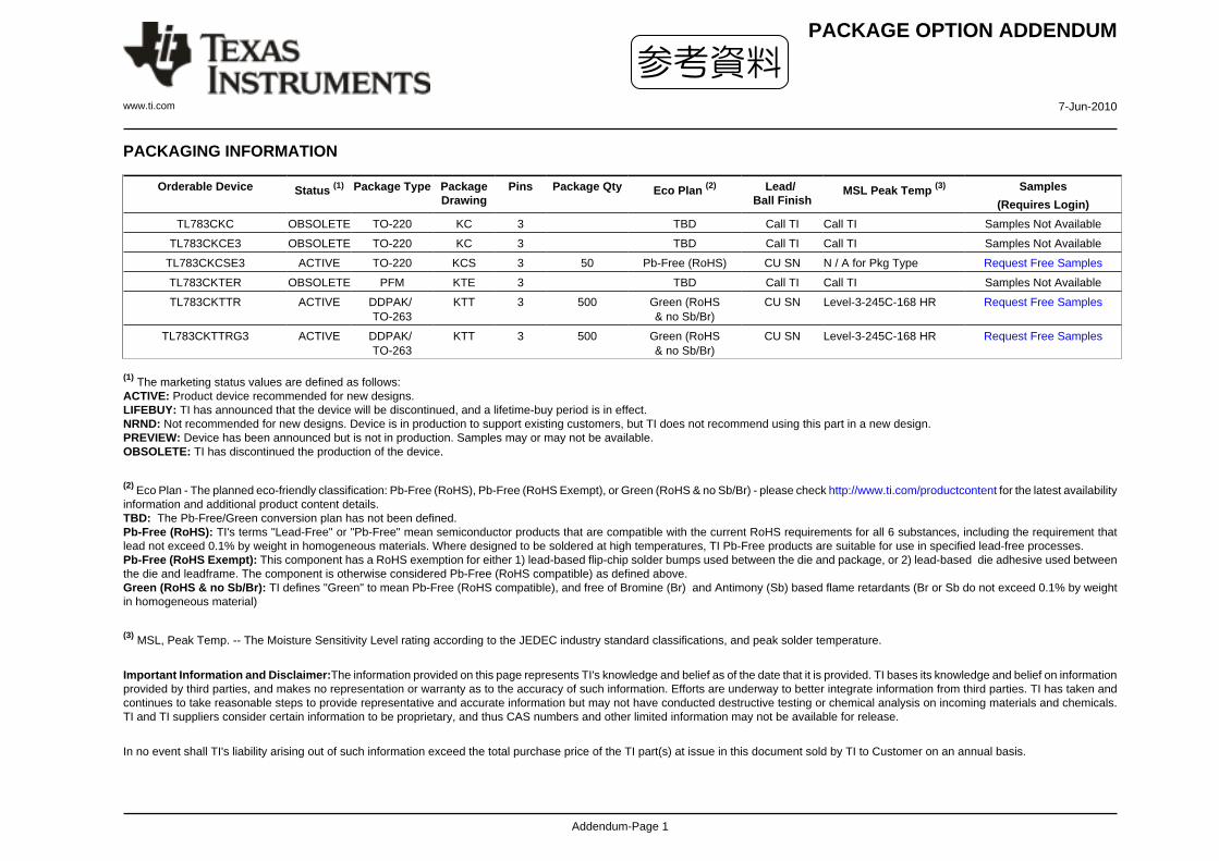
PACKAGE OPTION ADDENDUM
www.ti.com 7-Jun-2010
Addendum-Page 1
PACKAGING INFORMATION
Orderable Device Status (1) Package Type PackageDrawing
Pins Package Qty Eco Plan (2) Lead/Ball Finish
MSL Peak Temp (3) Samples
(Requires Login)
TL783CKC OBSOLETE TO-220 KC 3 TBD Call TI Call TI Samples Not Available
TL783CKCE3 OBSOLETE TO-220 KC 3 TBD Call TI Call TI Samples Not Available
TL783CKCSE3 ACTIVE TO-220 KCS 3 50 Pb-Free (RoHS) CU SN N / A for Pkg Type Request Free Samples
TL783CKTER OBSOLETE PFM KTE 3 TBD Call TI Call TI Samples Not Available
TL783CKTTR ACTIVE DDPAK/TO-263
KTT 3 500 Green (RoHS& no Sb/Br)
CU SN Level-3-245C-168 HR Request Free Samples
TL783CKTTRG3 ACTIVE DDPAK/TO-263
KTT 3 500 Green (RoHS& no Sb/Br)
CU SN Level-3-245C-168 HR Request Free Samples
(1) The marketing status values are defined as follows:ACTIVE: Product device recommended for new designs.LIFEBUY: TI has announced that the device will be discontinued, and a lifetime-buy period is in effect.NRND: Not recommended for new designs. Device is in production to support existing customers, but TI does not recommend using this part in a new design.PREVIEW: Device has been announced but is not in production. Samples may or may not be available.OBSOLETE: TI has discontinued the production of the device.
(2) Eco Plan - The planned eco-friendly classification: Pb-Free (RoHS), Pb-Free (RoHS Exempt), or Green (RoHS & no Sb/Br) - please check http://www.ti.com/productcontent for the latest availabilityinformation and additional product content details.TBD: The Pb-Free/Green conversion plan has not been defined.Pb-Free (RoHS): TI's terms "Lead-Free" or "Pb-Free" mean semiconductor products that are compatible with the current RoHS requirements for all 6 substances, including the requirement thatlead not exceed 0.1% by weight in homogeneous materials. Where designed to be soldered at high temperatures, TI Pb-Free products are suitable for use in specified lead-free processes.Pb-Free (RoHS Exempt): This component has a RoHS exemption for either 1) lead-based flip-chip solder bumps used between the die and package, or 2) lead-based die adhesive used betweenthe die and leadframe. The component is otherwise considered Pb-Free (RoHS compatible) as defined above.Green (RoHS & no Sb/Br): TI defines "Green" to mean Pb-Free (RoHS compatible), and free of Bromine (Br) and Antimony (Sb) based flame retardants (Br or Sb do not exceed 0.1% by weightin homogeneous material)
(3) MSL, Peak Temp. -- The Moisture Sensitivity Level rating according to the JEDEC industry standard classifications, and peak solder temperature.
Important Information and Disclaimer:The information provided on this page represents TI's knowledge and belief as of the date that it is provided. TI bases its knowledge and belief on informationprovided by third parties, and makes no representation or warranty as to the accuracy of such information. Efforts are underway to better integrate information from third parties. TI has taken andcontinues to take reasonable steps to provide representative and accurate information but may not have conducted destructive testing or chemical analysis on incoming materials and chemicals.TI and TI suppliers consider certain information to be proprietary, and thus CAS numbers and other limited information may not be available for release.
In no event shall TI's liability arising out of such information exceed the total purchase price of the TI part(s) at issue in this document sold by TI to Customer on an annual basis.
参考資料
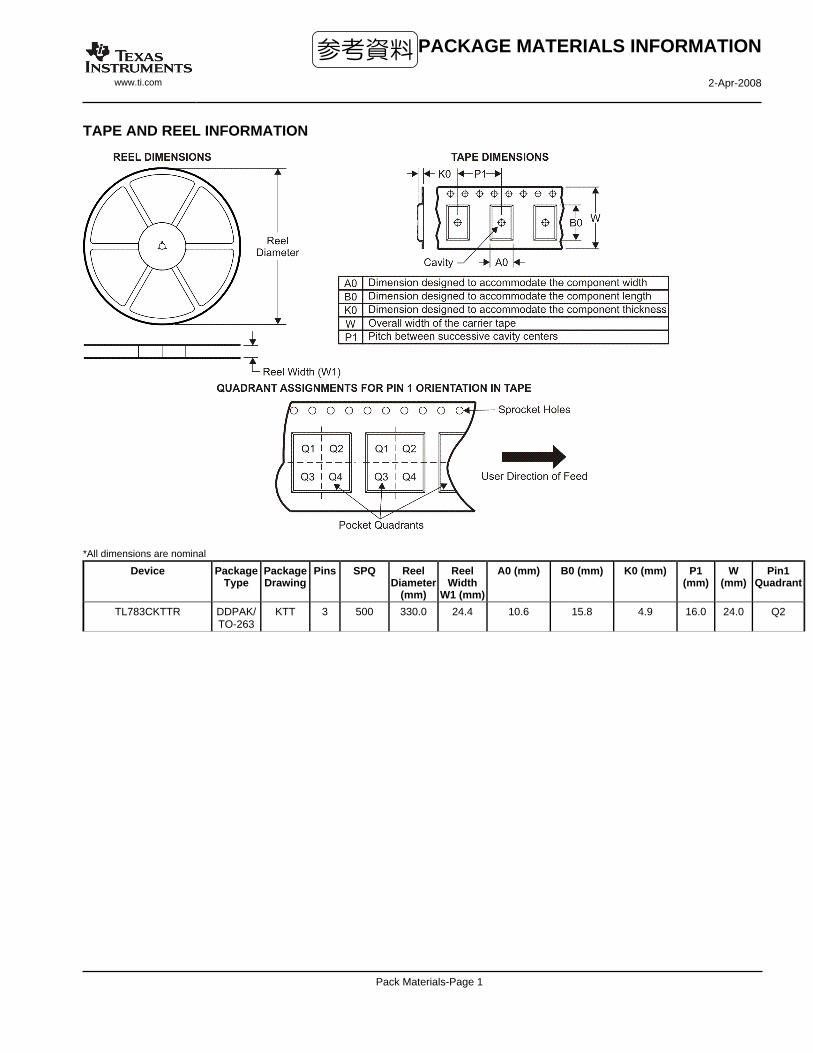
TAPE AND REEL INFORMATION
*All dimensions are nominal
Device PackageType
PackageDrawing
Pins SPQ ReelDiameter
(mm)
ReelWidth
W1 (mm)
A0 (mm) B0 (mm) K0 (mm) P1(mm)
W(mm)
Pin1Quadrant
TL783CKTTR DDPAK/TO-263
KTT 3 500 330.0 24.4 10.6 15.8 4.9 16.0 24.0 Q2
PACKAGE MATERIALS INFORMATION
www.ti.com 2-Apr-2008
Pack Materials-Page 1
参考資料

*All dimensions are nominal
Device Package Type Package Drawing Pins SPQ Length (mm) Width (mm) Height (mm)
TL783CKTTR DDPAK/TO-263 KTT 3 500 340.0 340.0 38.0
PACKAGE MATERIALS INFORMATION
www.ti.com 2-Apr-2008
Pack Materials-Page 2
参考資料

MECHANICAL DATA
MPFM001E – OCTOBER 1994 – REVISED JANUARY 2001
1POST OFFICE BOX 655303 • DALLAS, TEXAS 75265
KTE (R-PSFM-G3) PowerFLEX PLASTIC FLANGE-MOUNT
0.360 (9,14)0.350 (8,89)
0.080 (2,03)0.070 (1,78)
0.010 (0,25) NOM
0.040 (1,02)
Seating Plane
0.050 (1,27)
0.001 (0,03)0.005 (0,13)
0.010 (0,25)NOM
Gage Plane
0.010 (0,25)
0.031 (0,79)0.041 (1,04)
4073375/F 12/00
NOM
31
0.350 (8,89)
0.220 (5,59)
0.360 (9,14)
0.295 (7,49)NOM
0.320 (8,13)0.310 (7,87)
0.025 (0,63)
0.031 (0,79)
Thermal Tab(See Note C)
0.004 (0,10)M0.010 (0,25)0.100 (2,54)
3°–6°
0.410 (10,41)0.420 (10,67)
0.200 (5,08)
0.365 (9,27)
0.375 (9,52)
NOTES: A. All linear dimensions are in inches (millimeters).B. This drawing is subject to change without notice.C. The center lead is in electrical contact with the thermal tab.D. Dimensions do not include mold protrusions, not to exceed 0.006 (0,15).E. Falls within JEDEC MO-169
PowerFLEX is a trademark of Texas Instruments.
参考資料

参考資料
参考資料

参考資料

参考資料

IMPORTANT NOTICE
Texas Instruments Incorporated and its subsidiaries (TI) reserve the right to make corrections, enhancements, improvements and otherchanges to its semiconductor products and services per JESD46, latest issue, and to discontinue any product or service per JESD48, latestissue. Buyers should obtain the latest relevant information before placing orders and should verify that such information is current andcomplete. All semiconductor products (also referred to herein as “components”) are sold subject to TI’s terms and conditions of salesupplied at the time of order acknowledgment.
TI warrants performance of its components to the specifications applicable at the time of sale, in accordance with the warranty in TI’s termsand conditions of sale of semiconductor products. Testing and other quality control techniques are used to the extent TI deems necessaryto support this warranty. Except where mandated by applicable law, testing of all parameters of each component is not necessarilyperformed.
TI assumes no liability for applications assistance or the design of Buyers’ products. Buyers are responsible for their products andapplications using TI components. To minimize the risks associated with Buyers’ products and applications, Buyers should provideadequate design and operating safeguards.
TI does not warrant or represent that any license, either express or implied, is granted under any patent right, copyright, mask work right, orother intellectual property right relating to any combination, machine, or process in which TI components or services are used. Informationpublished by TI regarding third-party products or services does not constitute a license to use such products or services or a warranty orendorsement thereof. Use of such information may require a license from a third party under the patents or other intellectual property of thethird party, or a license from TI under the patents or other intellectual property of TI.
Reproduction of significant portions of TI information in TI data books or data sheets is permissible only if reproduction is without alterationand is accompanied by all associated warranties, conditions, limitations, and notices. TI is not responsible or liable for such altereddocumentation. Information of third parties may be subject to additional restrictions.
Resale of TI components or services with statements different from or beyond the parameters stated by TI for that component or servicevoids all express and any implied warranties for the associated TI component or service and is an unfair and deceptive business practice.TI is not responsible or liable for any such statements.
Buyer acknowledges and agrees that it is solely responsible for compliance with all legal, regulatory and safety-related requirementsconcerning its products, and any use of TI components in its applications, notwithstanding any applications-related information or supportthat may be provided by TI. Buyer represents and agrees that it has all the necessary expertise to create and implement safeguards whichanticipate dangerous consequences of failures, monitor failures and their consequences, lessen the likelihood of failures that might causeharm and take appropriate remedial actions. Buyer will fully indemnify TI and its representatives against any damages arising out of the useof any TI components in safety-critical applications.
In some cases, TI components may be promoted specifically to facilitate safety-related applications. With such components, TI’s goal is tohelp enable customers to design and create their own end-product solutions that meet applicable functional safety standards andrequirements. Nonetheless, such components are subject to these terms.
No TI components are authorized for use in FDA Class III (or similar life-critical medical equipment) unless authorized officers of the partieshave executed a special agreement specifically governing such use.
Only those TI components which TI has specifically designated as military grade or “enhanced plastic” are designed and intended for use inmilitary/aerospace applications or environments. Buyer acknowledges and agrees that any military or aerospace use of TI componentswhich have not been so designated is solely at the Buyer's risk, and that Buyer is solely responsible for compliance with all legal andregulatory requirements in connection with such use.
TI has specifically designated certain components which meet ISO/TS16949 requirements, mainly for automotive use. Components whichhave not been so designated are neither designed nor intended for automotive use; and TI will not be responsible for any failure of suchcomponents to meet such requirements.
Products Applications
Audio www.ti.com/audio Automotive and Transportation www.ti.com/automotive
Amplifiers amplifier.ti.com Communications and Telecom www.ti.com/communications
Data Converters dataconverter.ti.com Computers and Peripherals www.ti.com/computers
DLP® Products www.dlp.com Consumer Electronics www.ti.com/consumer-apps
DSP dsp.ti.com Energy and Lighting www.ti.com/energy
Clocks and Timers www.ti.com/clocks Industrial www.ti.com/industrial
Interface interface.ti.com Medical www.ti.com/medical
Logic logic.ti.com Security www.ti.com/security
Power Mgmt power.ti.com Space, Avionics and Defense www.ti.com/space-avionics-defense
Microcontrollers microcontroller.ti.com Video and Imaging www.ti.com/video
RFID www.ti-rfid.com
OMAP Applications Processors www.ti.com/omap TI E2E Community e2e.ti.com
Wireless Connectivity www.ti.com/wirelessconnectivity
Mailing Address: Texas Instruments, Post Office Box 655303, Dallas, Texas 75265Copyright © 2012, Texas Instruments Incorporated
参考資料