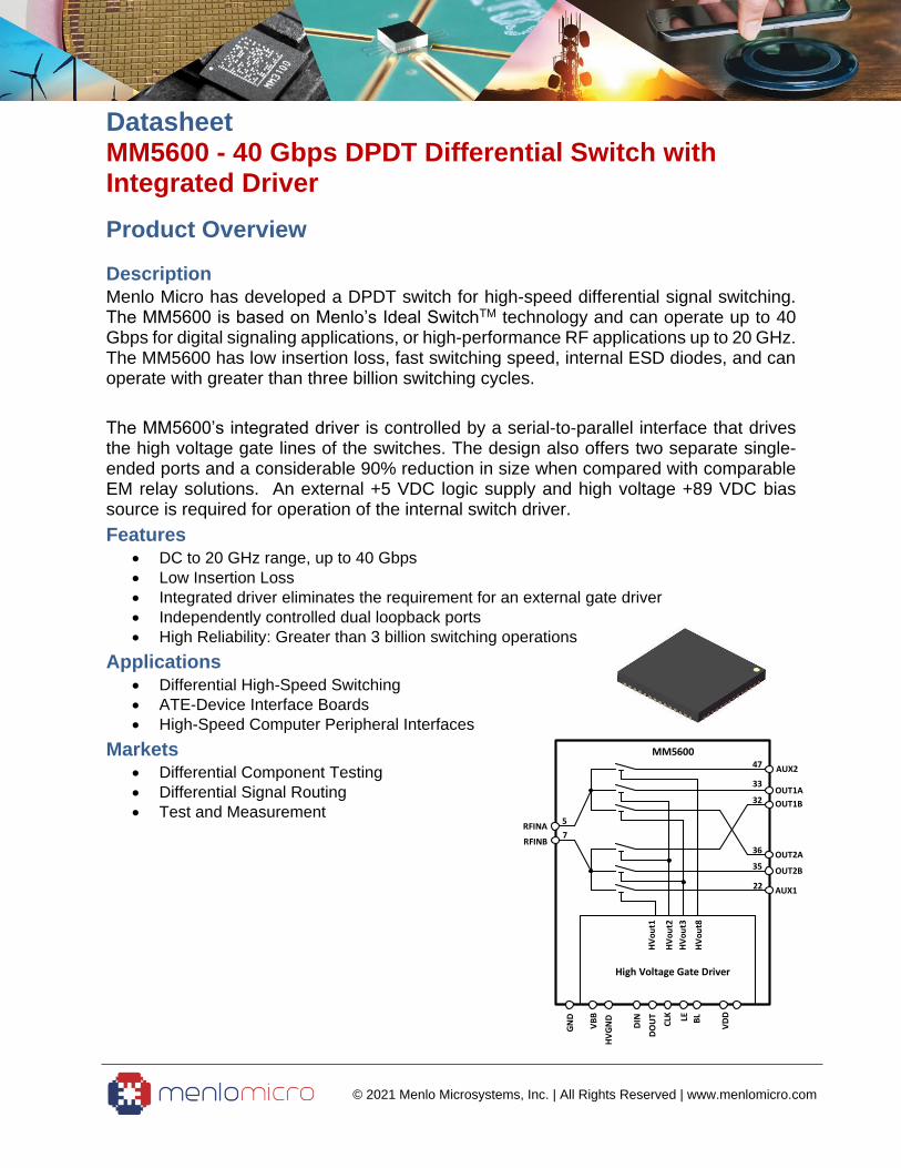
high voltage gate driver mm5600
TRANSCRIPT
© 2021 Menlo Microsystems, Inc. | All Rights Reserved | www.menlomicro.com
Datasheet MM5600 - 40 Gbps DPDT Differential Switch with Integrated Driver
Product Overview
Description Menlo Micro has developed a DPDT switch for high-speed differential signal switching. The MM5600 is based on Menlo’s Ideal SwitchTM technology and can operate up to 40 Gbps for digital signaling applications, or high-performance RF applications up to 20 GHz. The MM5600 has low insertion loss, fast switching speed, internal ESD diodes, and can operate with greater than three billion switching cycles.
The MM5600’s integrated driver is controlled by a serial-to-parallel interface that drives the high voltage gate lines of the switches. The design also offers two separate single-ended ports and a considerable 90% reduction in size when compared with comparable EM relay solutions. An external +5 VDC logic supply and high voltage +89 VDC bias source is required for operation of the internal switch driver.
Features • DC to 20 GHz range, up to 40 Gbps
• Low Insertion Loss
• Integrated driver eliminates the requirement for an external gate driver
• Independently controlled dual loopback ports
• High Reliability: Greater than 3 billion switching operations
Applications • Differential High-Speed Switching
• ATE-Device Interface Boards
• High-Speed Computer Peripheral Interfaces
Markets • Differential Component Testing
• Differential Signal Routing
• Test and Measurement
RFINA
RFINB
DIN CLK
HV
ou
t1
VB
B
DO
UT
VD
D
AUX1
OUT2B
AUX2
OUT1A
OUT2A
OUT1B
HV
GN
D
HV
ou
t2
HV
ou
t3
HV
ou
t8
MM5600
High Voltage Gate Driver
GN
D
5
7
47
22
33
32
36
35
LE BL
2 MM5600 - 40 Gbps DPDT Differential Switch | November 5, 2021 ver 2.0
© 2021 Menlo Microsystems, Inc. | All Rights Reserved | www.menlomicro.com
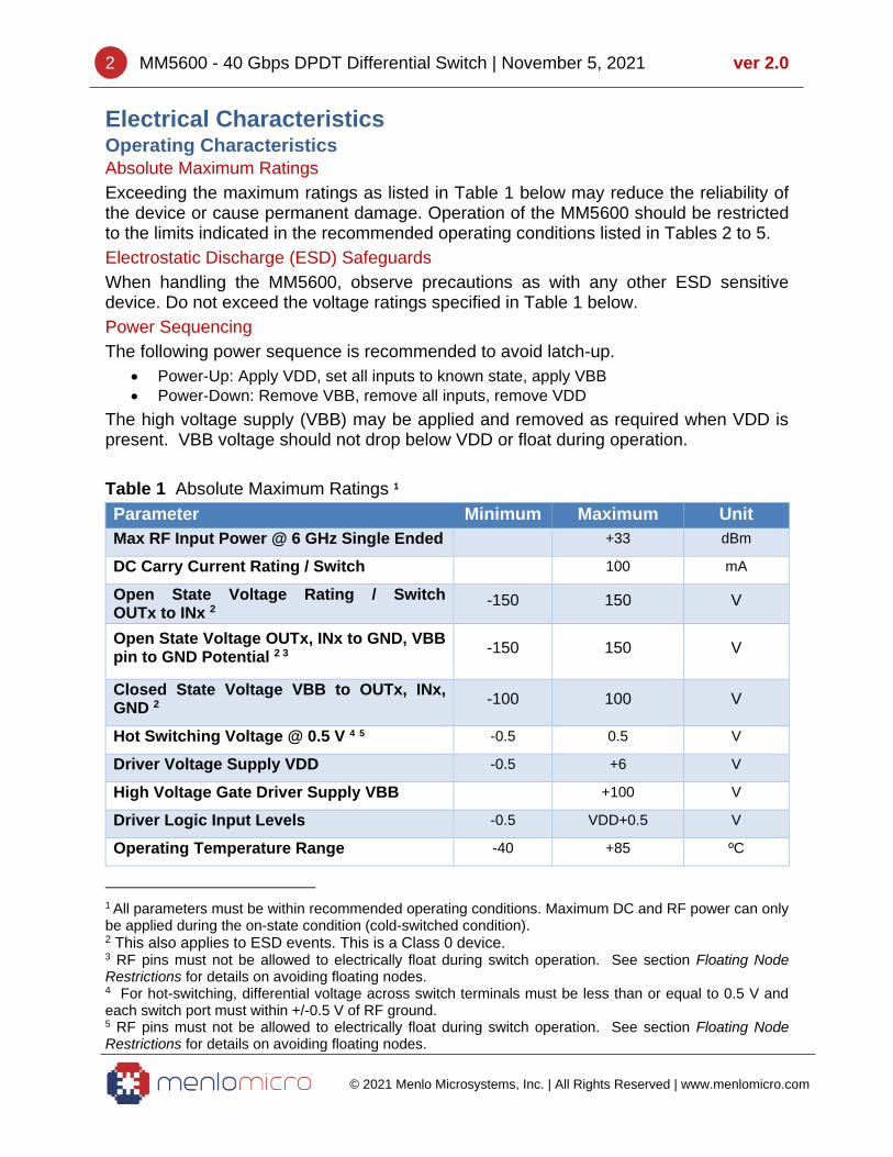
Electrical Characteristics Operating Characteristics Absolute Maximum Ratings
Exceeding the maximum ratings as listed in Table 1 below may reduce the reliability of the device or cause permanent damage. Operation of the MM5600 should be restricted to the limits indicated in the recommended operating conditions listed in Tables 2 to 5.
Electrostatic Discharge (ESD) Safeguards
When handling the MM5600, observe precautions as with any other ESD sensitive device. Do not exceed the voltage ratings specified in Table 1 below.
Power Sequencing
The following power sequence is recommended to avoid latch-up.
• Power-Up: Apply VDD, set all inputs to known state, apply VBB
• Power-Down: Remove VBB, remove all inputs, remove VDD
The high voltage supply (VBB) may be applied and removed as required when VDD is present. VBB voltage should not drop below VDD or float during operation.
Table 1 Absolute Maximum Ratings 1
Parameter Minimum Maximum Unit
Max RF Input Power @ 6 GHz Single Ended +33 dBm
DC Carry Current Rating / Switch 100 mA
Open State Voltage Rating / Switch OUTx to INx 2
-150 150 V
Open State Voltage OUTx, INx to GND, VBB pin to GND Potential 2 3
-150 150 V
Closed State Voltage VBB to OUTx, INx, GND 2
-100 100 V
Hot Switching Voltage @ 0.5 V 4 5 -0.5 0.5 V
Driver Voltage Supply VDD -0.5 +6 V
High Voltage Gate Driver Supply VBB +100 V
Driver Logic Input Levels -0.5 VDD+0.5 V
Operating Temperature Range -40 +85 ºC
1 All parameters must be within recommended operating conditions. Maximum DC and RF power can only be applied during the on-state condition (cold-switched condition). 2 This also applies to ESD events. This is a Class 0 device. 3 RF pins must not be allowed to electrically float during switch operation. See section Floating Node Restrictions for details on avoiding floating nodes. 4 For hot-switching, differential voltage across switch terminals must be less than or equal to 0.5 V and each switch port must within +/-0.5 V of RF ground. 5 RF pins must not be allowed to electrically float during switch operation. See section Floating Node Restrictions for details on avoiding floating nodes.
3 MM5600 - 40 Gbps DPDT Differential Switch | November 5, 2021 ver 2.0
© 2021 Menlo Microsystems, Inc. | All Rights Reserved | www.menlomicro.com
Storage Temperature Range6 -65 +150 ºC
ESD Rating HBM Driver Pins7 750 V
ESD Rating HBM RF I/O Pins8 9 500 V
Mechanical Shock10 500 G
Vibration11 500 Hz
DC and AC Electrical Specifications All specifications valid over full VBB range and operating temperature range unless otherwise noted.
Table 2 RF Characteristics
Parameter Minimum Typical12 Maximum Unit
Operating Frequency Range
Single-Ended mode
Differential mode
DC
DC
10
20
GHz
Max RF Power @ 3 GHz13 33 dBm
Insertion Loss
Single-Ended mode @ 10 GHz
1.3
dB
Input / Output Return Loss
Single-Ended mode @ 10 GHz
11
dB
Isolation
Single-Ended mode @ 10 GHz
24
dB
Third-Order Intercept Point (IP3)14 77 dBm
Second Harmonic (H2) 15 -102 dBc
Third Harmonic (H3)16 -101 dBc
6 See section Storage and Shelf Life for more information on shelf and floor life. 7 Driver pins include: CLK, BL, LE, DIN, DOUT, VBB, VDD. 8 RF I/O pins include: RFINA, RFINB, OUT1A, OUT1B, OUT2A, OUT2B, AUX1, AUX2. 9 RF I/O pin ESD rating of 500V is preliminary pending completion of qualification. 10 See JESD22-B104 for mechanical shock test methodology at 1.0 ms, half-sine, 5 shocks/axis, 6 axis. 11 See JESD22-B103 for vibration test methodology at 3.1 G and 30min/cycle, 1 cycle/axis, 3 axis. 12 Typical specifications represent the parametric norm. 13 Single Ended only 50 Ohms Measured at +85ºC.
14 Measured at +25ºC and 37dBm input power. 15 Measured at 2 GHz fundamental frequency and 33 dBm input power. 16 Measured at 2 GHz fundamental frequency and 33 dBm input power.
4 MM5600 - 40 Gbps DPDT Differential Switch | November 5, 2021 ver 2.0
© 2021 Menlo Microsystems, Inc. | All Rights Reserved | www.menlomicro.com
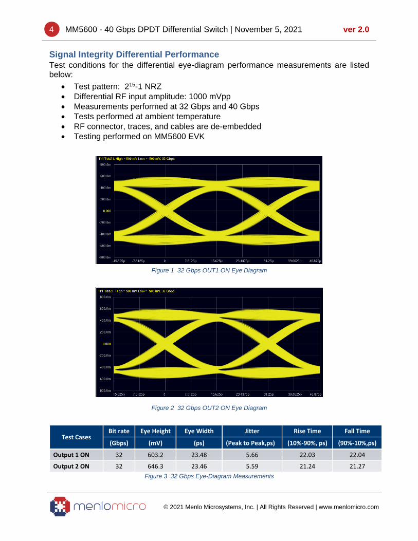
Signal Integrity Differential Performance Test conditions for the differential eye-diagram performance measurements are listed below:
• Test pattern: 215-1 NRZ
• Differential RF input amplitude: 1000 mVpp
• Measurements performed at 32 Gbps and 40 Gbps
• Tests performed at ambient temperature
• RF connector, traces, and cables are de-embedded
• Testing performed on MM5600 EVK
Figure 1 32 Gbps OUT1 ON Eye Diagram
Figure 2 32 Gbps OUT2 ON Eye Diagram
Test Cases Bit rate Eye Height Eye Width Jitter Rise Time Fall Time
(Gbps) (mV) (ps) (Peak to Peak,ps) (10%-90%, ps) (90%-10%,ps)
Output 1 ON 32 603.2 23.48 5.66 22.03 22.04
Output 2 ON 32 646.3 23.46 5.59 21.24 21.27
Figure 3 32 Gbps Eye-Diagram Measurements
5 MM5600 - 40 Gbps DPDT Differential Switch | November 5, 2021 ver 2.0
© 2021 Menlo Microsystems, Inc. | All Rights Reserved | www.menlomicro.com
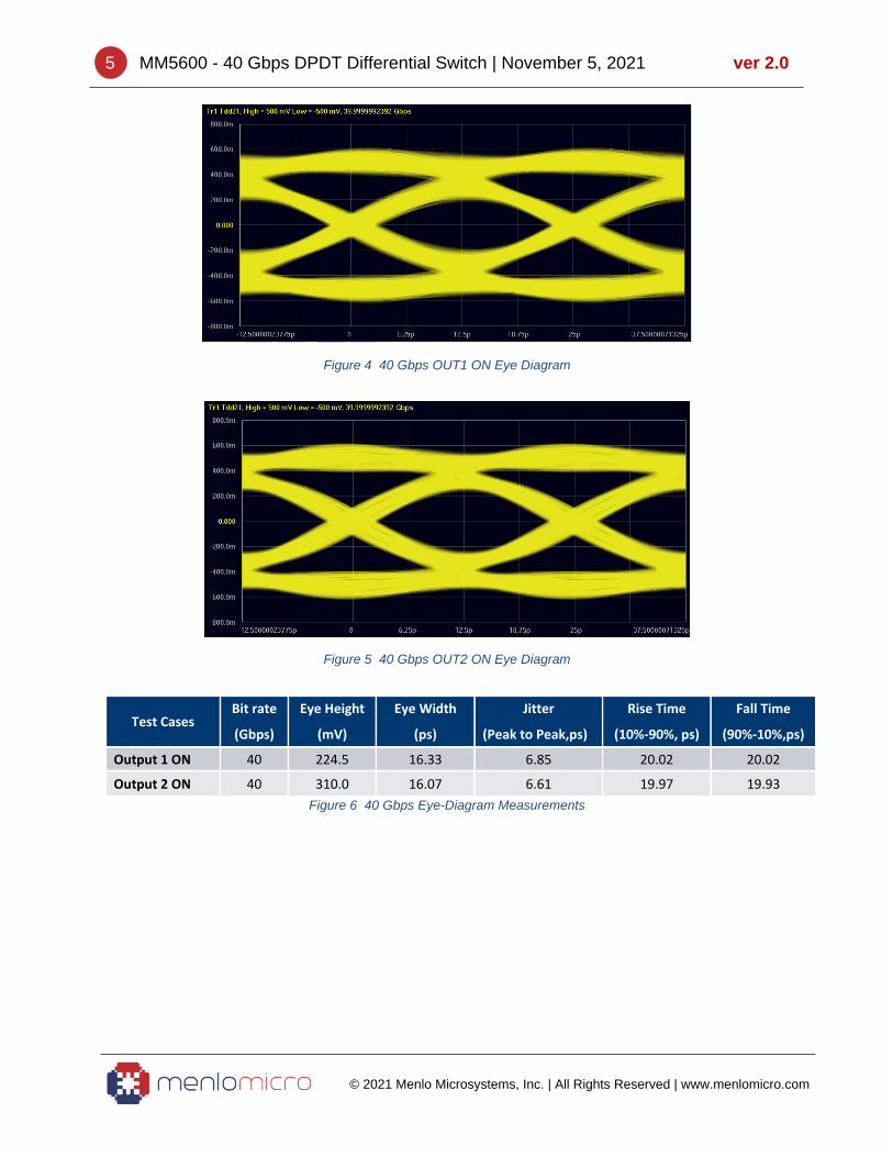
Figure 4 40 Gbps OUT1 ON Eye Diagram
Figure 5 40 Gbps OUT2 ON Eye Diagram
Test Cases Bit rate Eye Height Eye Width Jitter Rise Time Fall Time
(Gbps) (mV) (ps) (Peak to Peak,ps) (10%-90%, ps) (90%-10%,ps)
Output 1 ON 40 224.5 16.33 6.85 20.02 20.02
Output 2 ON 40 310.0 16.07 6.61 19.97 19.93
Figure 6 40 Gbps Eye-Diagram Measurements
6 MM5600 - 40 Gbps DPDT Differential Switch | November 5, 2021 ver 2.0
© 2021 Menlo Microsystems, Inc. | All Rights Reserved | www.menlomicro.com
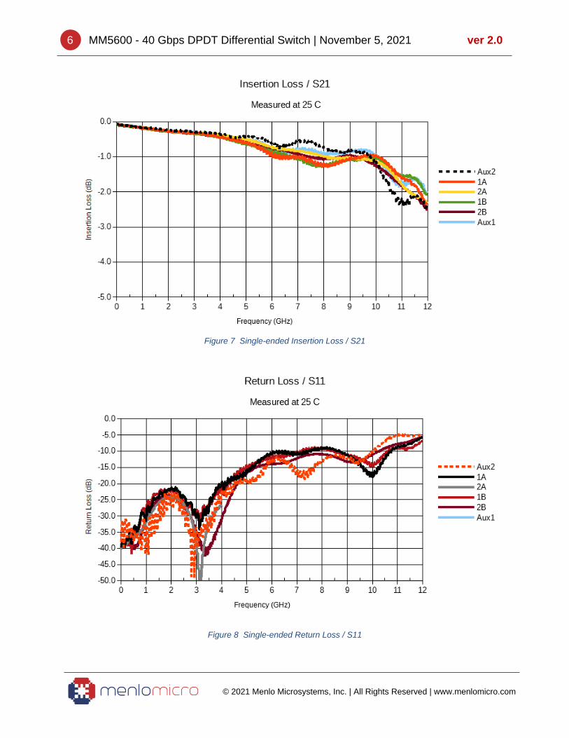
Figure 7 Single-ended Insertion Loss / S21
Figure 8 Single-ended Return Loss / S11
7 MM5600 - 40 Gbps DPDT Differential Switch | November 5, 2021 ver 2.0
© 2021 Menlo Microsystems, Inc. | All Rights Reserved | www.menlomicro.com
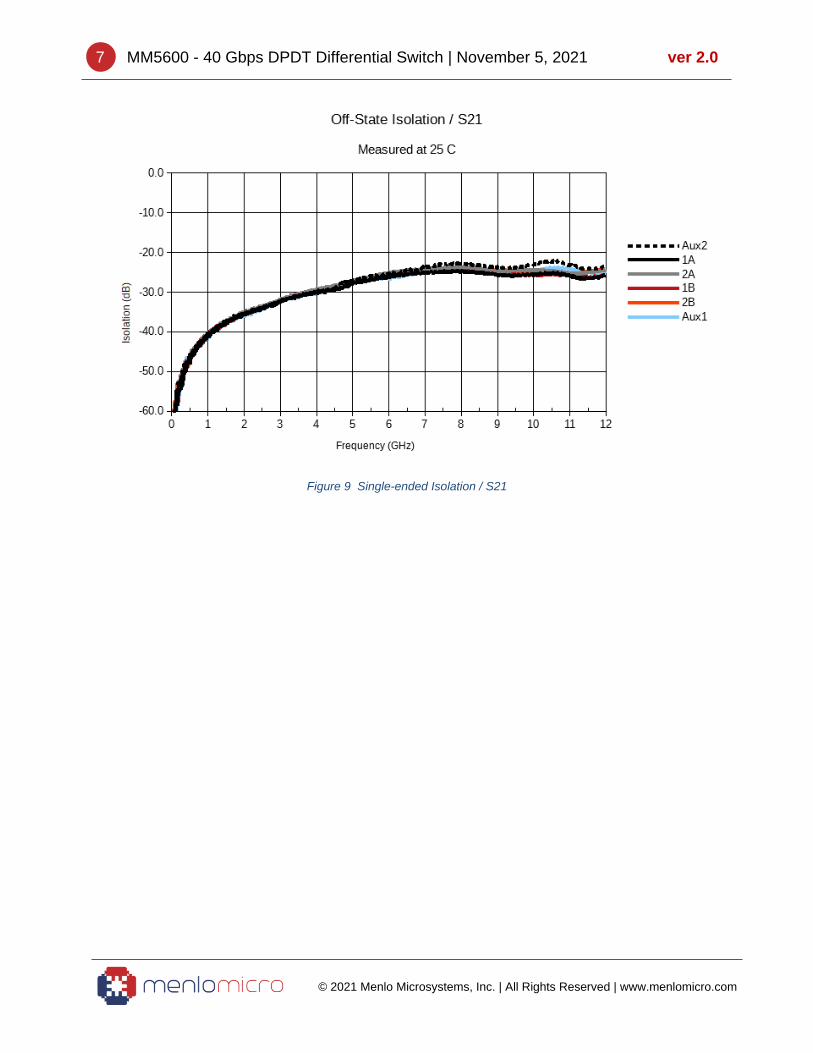
Figure 9 Single-ended Isolation / S21
8 MM5600 - 40 Gbps DPDT Differential Switch | November 5, 2021 ver 2.0
© 2021 Menlo Microsystems, Inc. | All Rights Reserved | www.menlomicro.com
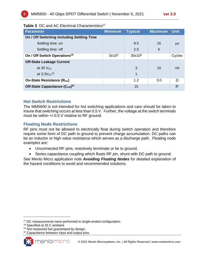
Table 3 DC and AC Electrical Characteristics17
Parameter Minimum Typical Maximum Unit
On / Off Switching including Settling Time
Settling time: on
Settling time: off
8.5
2.5
16
6
µs
On / Off Switch Operations18 3x10⁹ 30x109 Cycles
Off-State Leakage Current
at 30 VDC
at 3.3VDC19
3
1
10
nA
On-State Resistance (ROn) 1.2 3.0 Ω
Off-State Capacitance (COff)20 15 fF
Hot Switch Restrictions The MM5600 is not intended for hot switching applications and care should be taken to insure that switching occurs at less than 0.5 V. Further, the voltage at the switch terminals must be within +/-0.5 V relative to RF ground.
Floating Node Restrictions
RF pins must not be allowed to electrically float during switch operation and therefore require some form of DC path to ground to prevent charge accumulation. DC paths can be an inductor or high value resistance which serves as a discharge path. Floating node examples are:
• Unconnected RF pins, resistively terminate or tie to ground.
• Series capacitance coupling which floats RF pin, shunt with DC path to ground.
See Menlo Micro application note Avoiding Floating Nodes for detailed explanation of the hazard conditions to avoid and recommended solutions.
17 DC measurements were performed in single-ended configuration. 18 Specified at 25 C ambient. 19 Not measured but guaranteed by design. 20 Capacitance between input and output pins.
9 MM5600 - 40 Gbps DPDT Differential Switch | November 5, 2021 ver 2.0
© 2021 Menlo Microsystems, Inc. | All Rights Reserved | www.menlomicro.com
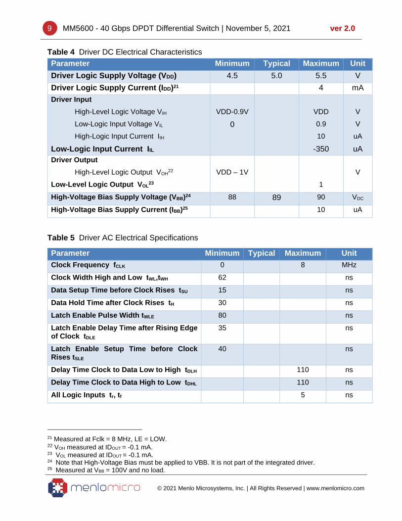
Table 4 Driver DC Electrical Characteristics
Parameter Minimum Typical Maximum Unit
Driver Logic Supply Voltage (VDD) 4.5 5.0 5.5 V
Driver Logic Supply Current (IDD)21 4 mA
Driver Input
High-Level Logic Voltage VIH
Low-Logic Input Voltage VIL
High-Logic Input Current IIH
Low-Logic Input Current IIL
VDD-0.9V
0
VDD
0.9
10
-350
V
V
uA
uA
Driver Output
High-Level Logic Output VOH22
Low-Level Logic Output VOL23
VDD – 1V
1
V
High-Voltage Bias Supply Voltage (VBB)24 88 89 90 VDC
High-Voltage Bias Supply Current (IBB)25 10 uA
Table 5 Driver AC Electrical Specifications
Parameter Minimum Typical Maximum Unit
Clock Frequency fCLK 0 8 MHz
Clock Width High and Low tWL,tWH 62 ns
Data Setup Time before Clock Rises tSU 15 ns
Data Hold Time after Clock Rises tH 30 ns
Latch Enable Pulse Width tWLE 80 ns
Latch Enable Delay Time after Rising Edge of Clock tDLE
35 ns
Latch Enable Setup Time before Clock Rises tSLE
40 ns
Delay Time Clock to Data Low to High tDLH 110 ns
Delay Time Clock to Data High to Low tDHL 110 ns
All Logic Inputs tr, tf 5 ns
21 Measured at Fclk = 8 MHz, LE = LOW. 22 VOH measured at IDOUT = -0.1 mA. 23 VOL measured at IDOUT = -0.1 mA. 24 Note that High-Voltage Bias must be applied to VBB. It is not part of the integrated driver. 25 Measured at VBB = 100V and no load.
10 MM5600 - 40 Gbps DPDT Differential Switch | November 5, 2021 ver 2.0
© 2021 Menlo Microsystems, Inc. | All Rights Reserved | www.menlomicro.com
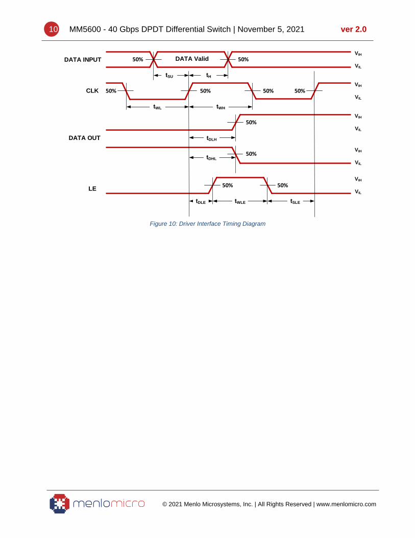
Figure 10: Driver Interface Timing Diagram
DATA INPUT
CLK
DATA OUT
LE
VIH
VIL
VIH
VIL
VIH
VIL
VIH
VIL
VIH
VIL
50% 50%
50% 50% 50% 50%
50%
50%
50%50%
tSU tH
tWL tWH
tDLH
tDHL
tDLE tWLE tSLE
DATA Valid
11 MM5600 - 40 Gbps DPDT Differential Switch | November 5, 2021 ver 2.0
© 2021 Menlo Microsystems, Inc. | All Rights Reserved | www.menlomicro.com
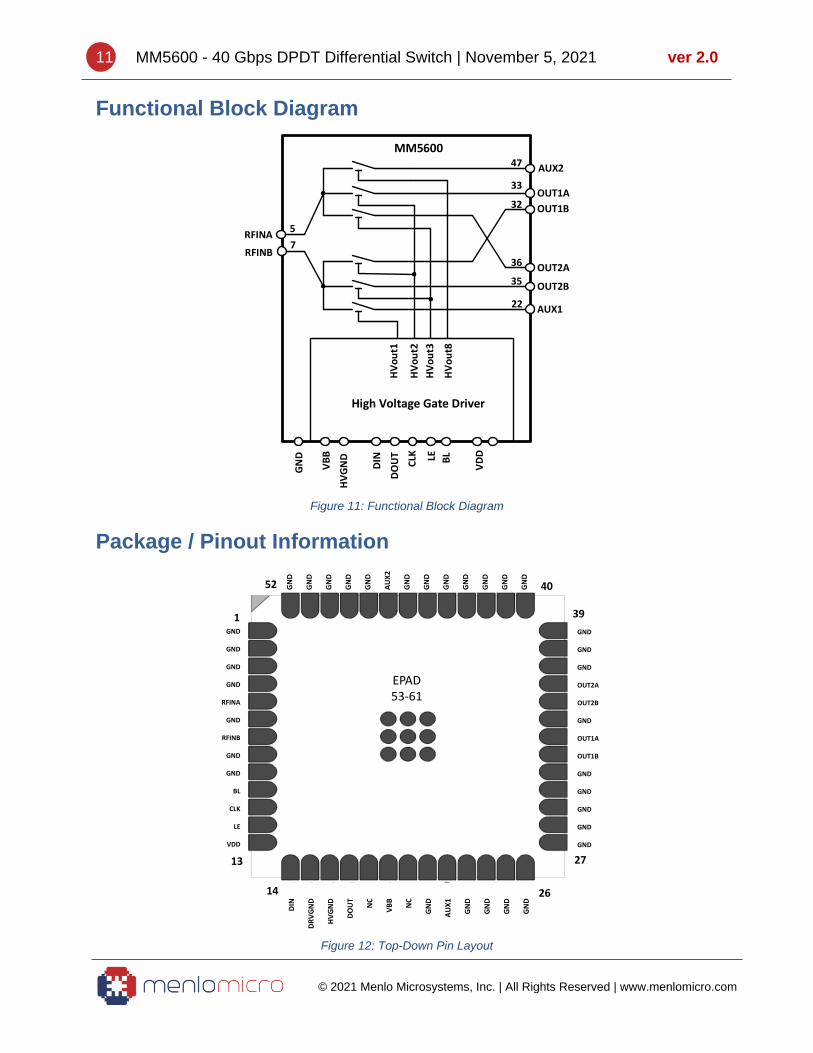
Functional Block Diagram
Figure 11: Functional Block Diagram
Package / Pinout Information
Figure 12: Top-Down Pin Layout
RFINA
RFINB
DIN CLK
HV
ou
t1
VB
B
DO
UT
VD
D
AUX1
OUT2B
AUX2
OUT1A
OUT2A
OUT1B
HV
GN
D
HV
ou
t2
HV
ou
t3
HV
ou
t8
MM5600
High Voltage Gate Driver
GN
D
5
7
47
22
33
32
36
35
LE BL
1
14
27
40
53 - 61
GND
GND
GND
GND
RFINA
GND
RFINB
GND
GND
BL
CLK
LE
VDD
GND
GND
GND
OUT2A
OUT2B
GND
OUT1A
OUT1B
GND
GND
GND
GND
GND
GN
D
GN
D
GN
D
GN
D
GN
D
AU
X2
GN
D
GN
D
GN
D
GN
D
GN
D
GN
D
GN
D
DIN
DR
VG
ND
HV
GN
D
DO
UT
NC
VB
B
NC
GN
D
AU
X1
GN
D
GN
D
GN
D
GN
D
13
26
39
52
EPADEPAD53-61
12 MM5600 - 40 Gbps DPDT Differential Switch | November 5, 2021 ver 2.0
© 2021 Menlo Microsystems, Inc. | All Rights Reserved | www.menlomicro.com
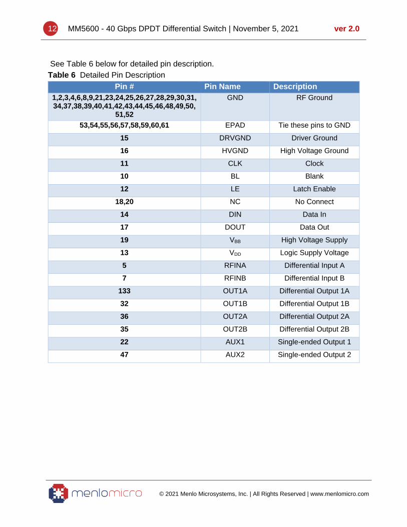
See Table 6 below for detailed pin description.
Table 6 Detailed Pin Description
Pin # Pin Name Description
1,2,3,4,6,8,9,21,23,24,25,26,27,28,29,30,31,34,37,38,39,40,41,42,43,44,45,46,48,49,50,
51,52
GND RF Ground
53,54,55,56,57,58,59,60,61 EPAD Tie these pins to GND
15 DRVGND Driver Ground
16 HVGND High Voltage Ground
11 CLK Clock
10 BL Blank
12 LE Latch Enable
18,20 NC No Connect
14 DIN Data In
17 DOUT Data Out
19 VBB High Voltage Supply
13 VDD Logic Supply Voltage
5 RFINA Differential Input A
7 RFINB Differential Input B
133 OUT1A Differential Output 1A
32 OUT1B Differential Output 1B
36 OUT2A Differential Output 2A
35 OUT2B Differential Output 2B
22 AUX1 Single-ended Output 1
47 AUX2 Single-ended Output 2
13 MM5600 - 40 Gbps DPDT Differential Switch | November 5, 2021 ver 2.0
© 2021 Menlo Microsystems, Inc. | All Rights Reserved | www.menlomicro.com
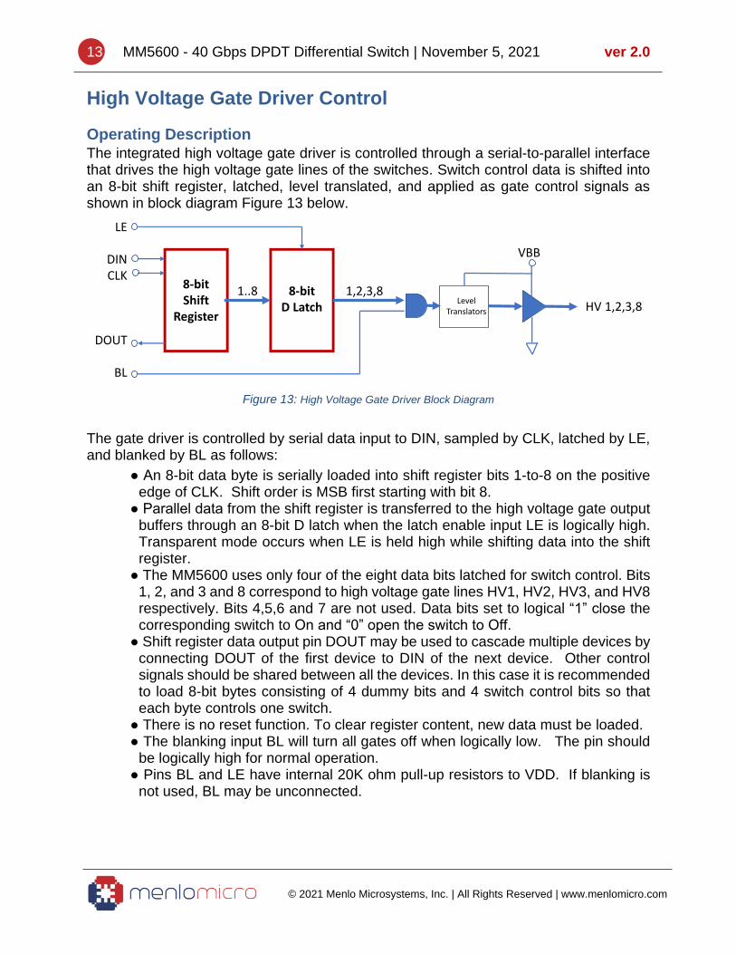
High Voltage Gate Driver Control
Operating Description The integrated high voltage gate driver is controlled through a serial-to-parallel interface that drives the high voltage gate lines of the switches. Switch control data is shifted into an 8-bit shift register, latched, level translated, and applied as gate control signals as shown in block diagram Figure 13 below.
Figure 13: High Voltage Gate Driver Block Diagram
The gate driver is controlled by serial data input to DIN, sampled by CLK, latched by LE, and blanked by BL as follows:
An 8-bit data byte is serially loaded into shift register bits 1-to-8 on the positive edge of CLK. Shift order is MSB first starting with bit 8.
Parallel data from the shift register is transferred to the high voltage gate output buffers through an 8-bit D latch when the latch enable input LE is logically high. Transparent mode occurs when LE is held high while shifting data into the shift register.
The MM5600 uses only four of the eight data bits latched for switch control. Bits 1, 2, and 3 and 8 correspond to high voltage gate lines HV1, HV2, HV3, and HV8 respectively. Bits 4,5,6 and 7 are not used. Data bits set to logical “1” close the corresponding switch to On and “0” open the switch to Off.
Shift register data output pin DOUT may be used to cascade multiple devices by connecting DOUT of the first device to DIN of the next device. Other control signals should be shared between all the devices. In this case it is recommended to load 8-bit bytes consisting of 4 dummy bits and 4 switch control bits so that each byte controls one switch.
There is no reset function. To clear register content, new data must be loaded. The blanking input BL will turn all gates off when logically low. The pin should
be logically high for normal operation. Pins BL and LE have internal 20K ohm pull-up resistors to VDD. If blanking is
not used, BL may be unconnected.
8-bitShift
Register
8-bitD Latch
LE
DINCLK
DOUT
BL
1..8 1,2,3,8Level
Translators HV 1,2,3,8
VBB
14 MM5600 - 40 Gbps DPDT Differential Switch | November 5, 2021 ver 2.0
© 2021 Menlo Microsystems, Inc. | All Rights Reserved | www.menlomicro.com
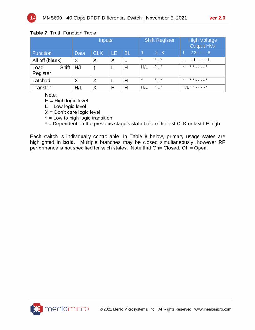
Table 7 Truth Function Table
Inputs Shift Register High Voltage Output HVx
Function Data CLK LE BL 1 2…8 1 2 3 - - - - 8
All off (blank) X X X L * *…* L L L - - - - L
Load Shift Register
H/L ↑ L H H/L *…* * * * - - - - *
Latched X X L H * *…* * * * - - - - *
Transfer H/L X H H H/L *…* H/L * * - - - - *
Note: H = High logic level L = Low logic level X = Don’t care logic level ↑ = Low to high logic transition * = Dependent on the previous stage’s state before the last CLK or last LE high
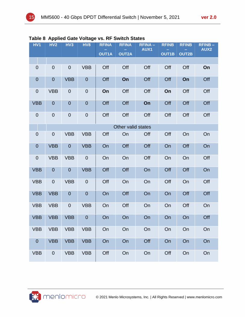
Each switch is individually controllable. In Table 8 below, primary usage states are highlighted in bold. Multiple branches may be closed simultaneously, however RF performance is not specified for such states. Note that On= Closed, Off = Open.
15 MM5600 - 40 Gbps DPDT Differential Switch | November 5, 2021 ver 2.0
© 2021 Menlo Microsystems, Inc. | All Rights Reserved | www.menlomicro.com
Table 8 Applied Gate Voltage vs. RF Switch States
HV1 HV2 HV3 HV8 RFINA –
OUT1A
RFINA –
OUT2A
RFINA – AUX1
RFINB –
OUT1B
RFINB –
OUT2B
RFINB – AUX2
0 0 0 VBB Off Off Off Off Off On
0 0 VBB 0 Off On Off Off On Off
0 VBB 0 0 On Off Off On Off Off
VBB 0 0 0 Off Off On Off Off Off
0 0 0 0 Off Off Off Off Off Off
Other valid states
0 0 VBB VBB Off On Off Off On On
0 VBB 0 VBB On Off Off On Off On
0 VBB VBB 0 On On Off On On Off
VBB 0 0 VBB Off Off On Off Off On
VBB 0 VBB 0 Off On On Off On Off
VBB VBB 0 0 On Off On On Off Off
VBB VBB 0 VBB On Off On On Off On
VBB VBB VBB 0 On On On On On Off
VBB VBB VBB VBB On On On On On On
0 VBB VBB VBB On On Off On On On
VBB 0 VBB VBB Off On On Off On On
16 MM5600 - 40 Gbps DPDT Differential Switch | November 5, 2021 ver 2.0
© 2021 Menlo Microsystems, Inc. | All Rights Reserved | www.menlomicro.com
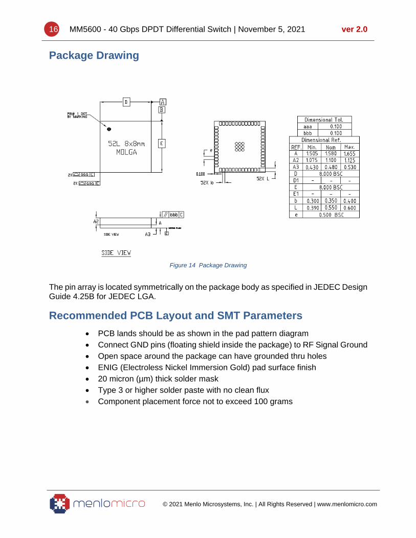
Package Drawing
Figure 14 Package Drawing
The pin array is located symmetrically on the package body as specified in JEDEC Design Guide 4.25B for JEDEC LGA.
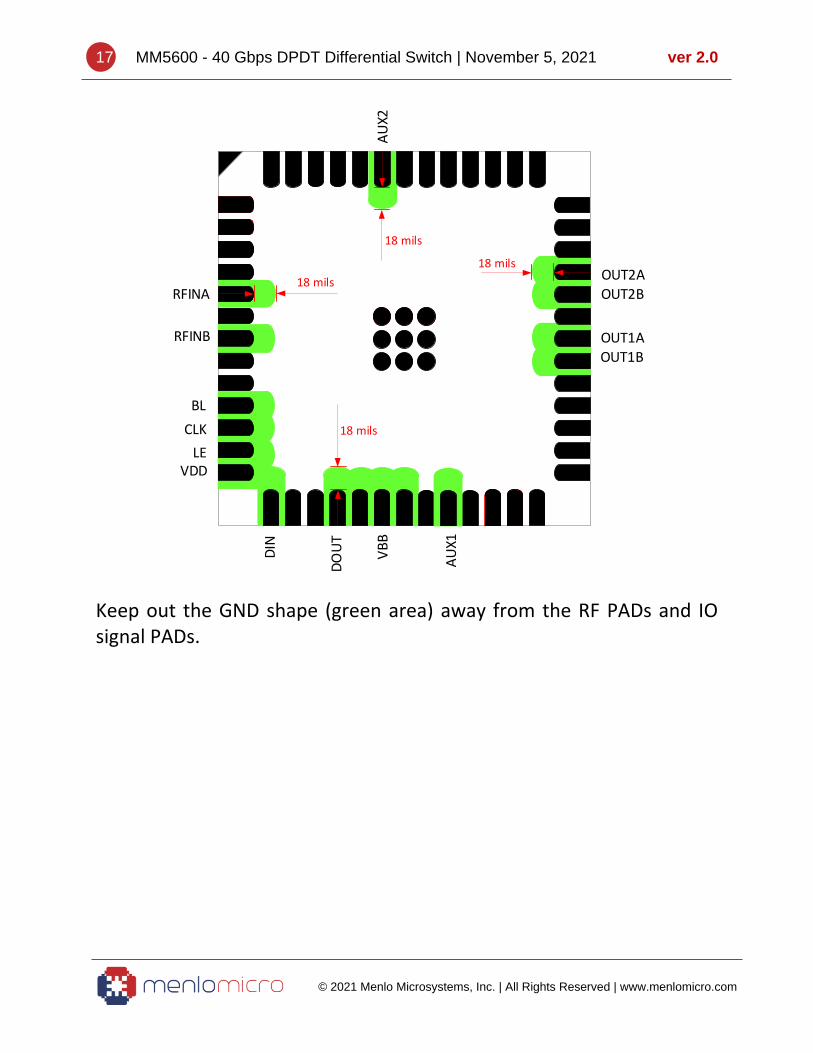
Recommended PCB Layout and SMT Parameters
• PCB lands should be as shown in the pad pattern diagram
• Connect GND pins (floating shield inside the package) to RF Signal Ground
• Open space around the package can have grounded thru holes
• ENIG (Electroless Nickel Immersion Gold) pad surface finish
• 20 micron (µm) thick solder mask
• Type 3 or higher solder paste with no clean flux
• Component placement force not to exceed 100 grams
17 MM5600 - 40 Gbps DPDT Differential Switch | November 5, 2021 ver 2.0
© 2021 Menlo Microsystems, Inc. | All Rights Reserved | www.menlomicro.com
18 mils
18 mils
18 mils
18 mils
RFINA
RFINB
BL
CLK
LEVDD
OUT2A
OUT2B
OUT1A
OUT1B
AU
X2
AU
X1
VB
B
DO
UT
DIN
Keep out the GND shape (green area) away from the RF PADs and IO signal PADs.
18 MM5600 - 40 Gbps DPDT Differential Switch | November 5, 2021 ver 2.0
© 2021 Menlo Microsystems, Inc. | All Rights Reserved | www.menlomicro.com
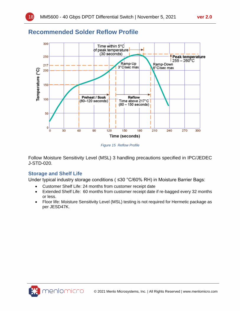
Recommended Solder Reflow Profile
Figure 15 Reflow Profile
Follow Moisture Sensitivity Level (MSL) 3 handling precautions specified in IPC/JEDEC J-STD-020.
Storage and Shelf Life Under typical industry storage conditions ( ≤30 °C/60% RH) in Moisture Barrier Bags:
• Customer Shelf Life: 24 months from customer receipt date
• Extended Shelf Life: 60 months from customer receipt date if re-bagged every 32 months or less.
• Floor life: Moisture Sensitivity Level (MSL) testing is not required for Hermetic package as per JESD47K.
19 MM5600 - 40 Gbps DPDT Differential Switch | November 5, 2021 ver 2.0
© 2021 Menlo Microsystems, Inc. | All Rights Reserved | www.menlomicro.com
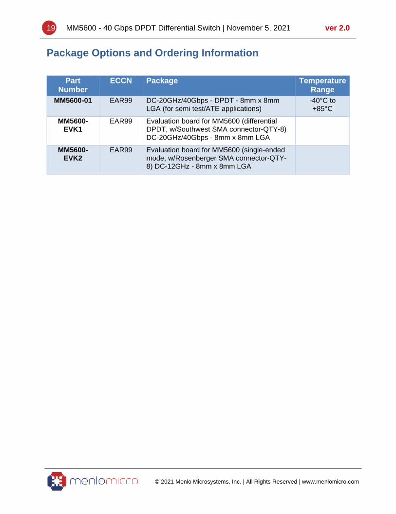
Package Options and Ordering Information
Part Number
ECCN Package Temperature Range
MM5600-01 EAR99 DC-20GHz/40Gbps - DPDT - 8mm x 8mm LGA (for semi test/ATE applications)
-40°C to +85°C
MM5600-EVK1
EAR99 Evaluation board for MM5600 (differential DPDT, w/Southwest SMA connector-QTY-8) DC-20GHz/40Gbps - 8mm x 8mm LGA
MM5600-EVK2
EAR99 Evaluation board for MM5600 (single-ended mode, w/Rosenberger SMA connector-QTY-8) DC-12GHz - 8mm x 8mm LGA

20 MM5600 - 40 Gbps DPDT Differential Switch | November 5, 2021 ver 2.0
© 2021 Menlo Microsystems, Inc. | All Rights Reserved | www.menlomicro.com
Important Information
Disclaimer The data presented in this document is for informational purposes only and shall in no event be regarded as a guarantee of conditions or characteristics. Any warranty or license for this product shall be specified and governed by the terms of a separate purchase agreement. Menlo Micro does not assume any liability arising out of the application or use of this product; neither does it convey any license under its patent rights, nor the rights of others.
Menlo Micro reserves the right to make changes in these specifications and features shown herein to improve reliability, function and design, or discontinue of this product, at any time without notice or obligation. Contact our product representative for the most current information.
Warning This product is not authorized for use:
1) In any life support systems. 2) Applications for implanting into the human body, without the express written
approval from Menlo Micro.
Trademark Notices All trademarks and product service marks are owned by Menlo Microsystems, Inc.
Contact Information Please contact Menlo Micro for the latest specifications, additional product information, test and evaluation boards, product samples, worldwide sales and distribution locations:
Internet: www.menlomicro.com
E-mail: [email protected]
For product technical questions and application information: [email protected].