high-voltage, high-current operational … high-current operational amplifier description the opa548...
TRANSCRIPT
OPA548
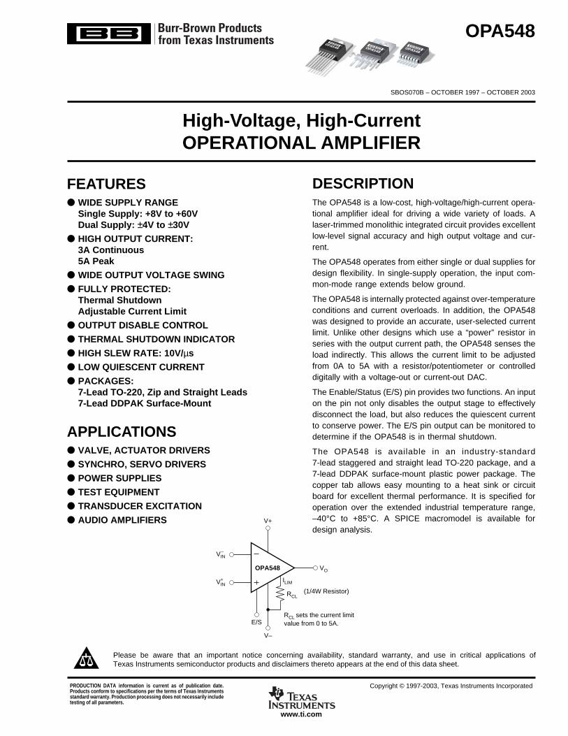
VIN–
VIN+
V+
E/S
RCL
RCL sets the current limitvalue from 0 to 5A.
(1/4W Resistor)
ILIM
VO
V–
High-Voltage, High-CurrentOPERATIONAL AMPLIFIER
DESCRIPTIONThe OPA548 is a low-cost, high-voltage/high-current opera-tional amplifier ideal for driving a wide variety of loads. Alaser-trimmed monolithic integrated circuit provides excellentlow-level signal accuracy and high output voltage and cur-rent.
The OPA548 operates from either single or dual supplies fordesign flexibility. In single-supply operation, the input com-mon-mode range extends below ground.
The OPA548 is internally protected against over-temperatureconditions and current overloads. In addition, the OPA548was designed to provide an accurate, user-selected currentlimit. Unlike other designs which use a “power” resistor inseries with the output current path, the OPA548 senses theload indirectly. This allows the current limit to be adjustedfrom 0A to 5A with a resistor/potentiometer or controlleddigitally with a voltage-out or current-out DAC.
The Enable/Status (E/S) pin provides two functions. An inputon the pin not only disables the output stage to effectivelydisconnect the load, but also reduces the quiescent currentto conserve power. The E/S pin output can be monitored todetermine if the OPA548 is in thermal shutdown.
The OPA548 is available in an industry-standard7-lead staggered and straight lead TO-220 package, and a7-lead DDPAK surface-mount plastic power package. Thecopper tab allows easy mounting to a heat sink or circuitboard for excellent thermal performance. It is specified foroperation over the extended industrial temperature range,–40°C to +85°C. A SPICE macromodel is available fordesign analysis.
FEATURES WIDE SUPPLY RANGE
Single Supply: +8V to +60VDual Supply: ±4V to ±30V
HIGH OUTPUT CURRENT:3A Continuous5A Peak
WIDE OUTPUT VOLTAGE SWING
FULLY PROTECTED:Thermal ShutdownAdjustable Current Limit
OUTPUT DISABLE CONTROL
THERMAL SHUTDOWN INDICATOR
HIGH SLEW RATE: 10V/µs
LOW QUIESCENT CURRENT
PACKAGES:7-Lead TO-220, Zip and Straight Leads7-Lead DDPAK Surface-Mount
APPLICATIONS VALVE, ACTUATOR DRIVERS
SYNCHRO, SERVO DRIVERS
POWER SUPPLIES
TEST EQUIPMENT
TRANSDUCER EXCITATION
AUDIO AMPLIFIERS
OPA548
SBOS070B – OCTOBER 1997 – OCTOBER 2003
www.ti.com
PRODUCTION DATA information is current as of publication date.Products conform to specifications per the terms of Texas Instrumentsstandard warranty. Production processing does not necessarily includetesting of all parameters.
Copyright © 1997-2003, Texas Instruments Incorporated
Please be aware that an important notice concerning availability, standard warranty, and use in critical applications ofTexas Instruments semiconductor products and disclaimers thereto appears at the end of this data sheet.
OPA548
OPA548 OPA548
OPA5482SBOS070Bwww.ti.com
ABSOLUTE MAXIMUM RATINGS(1)
Output Current ................................................................. See SOA CurveSupply Voltage, V+ to V– ................................................................... 60VInput Voltage .................................................. (V–) – 0.5V to (V+) + 0.5VInput Shutdown Voltage ........................................................................ V+Operating Temperature ..................................................–40°C to +125°CStorage Temperature .....................................................–55°C to +125°CJunction Temperature ...................................................................... 150°CLead Temperature (soldering 10s)(2) .............................................. 300°C
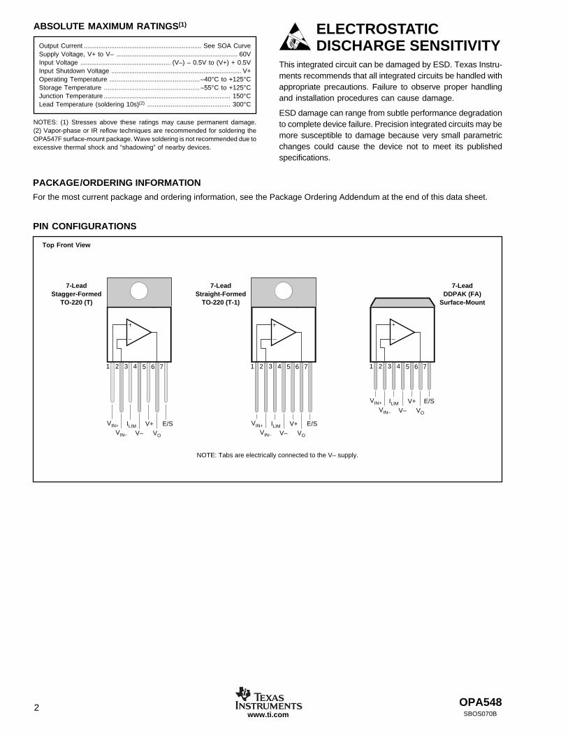
Top Front View
PIN CONFIGURATIONS
NOTES: (1) Stresses above these ratings may cause permanent damage.(2) Vapor-phase or IR reflow techniques are recommended for soldering theOPA547F surface-mount package. Wave soldering is not recommended due toexcessive thermal shock and “shadowing” of nearby devices.
PACKAGE/ORDERING INFORMATION
For the most current package and ordering information, see the Package Ordering Addendum at the end of this data sheet.
ELECTROSTATICDISCHARGE SENSITIVITY
This integrated circuit can be damaged by ESD. Texas Instru-ments recommends that all integrated circuits be handled withappropriate precautions. Failure to observe proper handlingand installation procedures can cause damage.
ESD damage can range from subtle performance degradationto complete device failure. Precision integrated circuits may bemore susceptible to damage because very small parametricchanges could cause the device not to meet its publishedspecifications.
7-LeadStraight-Formed
TO-220 (T-1)
NOTE: Tabs are electrically connected to the V– supply.
ILIM
V– VO
V+VIN–
VIN+
1 2 3 4 5 6
E/S
7
7-LeadDDPAK (FA)
Surface-Mount
ILIM
V– VO
V+VIN–
VIN+
1 2 3 4 5 6
E/S
7
7-LeadStagger-Formed
TO-220 (T)
ILIM
V– VO
V+VIN–
VIN+
1 2 3 4 5 6
E/S
7
OPA548 3SBOS070B www.ti.com
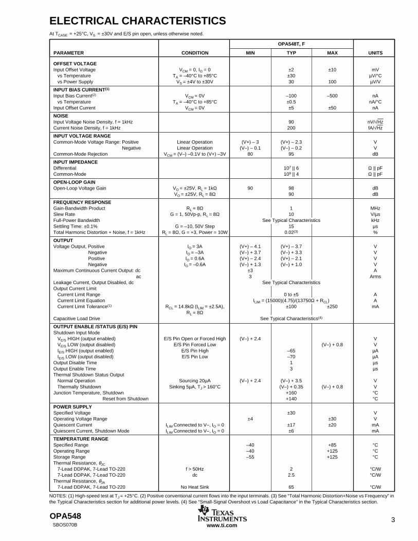
ELECTRICAL CHARACTERISTICSAt TCASE = +25°C, VS = ±30V and E/S pin open, unless otherwise noted.
OPA548T, F
PARAMETER CONDITION MIN TYP MAX UNITS
OFFSET VOLTAGEInput Offset Voltage VCM = 0, IO = 0 ±2 ±10 mV
vs Temperature TA = –40°C to +85°C ±30 µV/°Cvs Power Supply VS = ±4V to ±30V 30 100 µV/V
INPUT BIAS CURRENT(1)
Input Bias Current(2) VCM = 0V –100 –500 nAvs Temperature TA = –40°C to +85°C ±0.5 nA/°C
Input Offset Current VCM = 0V ±5 ±50 nA
NOISEInput Voltage Noise Density, f = 1kHz 90 nV/√HzCurrent Noise Density, f = 1kHz 200 fA/√Hz
INPUT VOLTAGE RANGECommon-Mode Voltage Range: Positive Linear Operation (V+) – 3 (V+) – 2.3 V
Negative Linear Operation (V–) – 0.1 (V–) – 0.2 VCommon-Mode Rejection VCM = (V–) –0.1V to (V+) –3V 80 95 dB
INPUT IMPEDANCEDifferential 107 || 6 Ω || pFCommon-Mode 109 || 4 Ω || pF
OPEN-LOOP GAINOpen-Loop Voltage Gain VO = ±25V, RL = 1kΩ 90 98 dB
VO = ±25V, RL = 8Ω 90 dB
FREQUENCY RESPONSEGain-Bandwidth Product RL = 8Ω 1 MHzSlew Rate G = 1, 50Vp-p, RL = 8Ω 10 V/µsFull-Power Bandwidth See Typical Characteristics kHzSettling Time: ±0.1% G = –10, 50V Step 15 µsTotal Harmonic Distortion + Noise, f = 1kHz RL = 8Ω, G = +3, Power = 10W 0.02(3) %
OUTPUTVoltage Output, Positive IO = 3A (V+) – 4.1 (V+) – 3.7 V
Negative IO = –3A (V–) + 3.7 (V–) + 3.3 VPositive IO = 0.6A (V+) – 2.4 (V+) – 2.1 VNegative IO = –0.6A (V–) + 1.3 (V–) + 1.0 V
Maximum Continuous Current Output: dc ±3 Aac 3 Arms
Leakage Current, Output Disabled, dc See Typical CharacteristicsOutput Current Limit
Current Limit Range 0 to ±5 ACurrent Limit Equation ILIM = (15000)(4.75)/(13750Ω + RCL) ACurrent Limit Tolerance(1) RCL = 14.8kΩ (ILIM = ±2.5A), ±100 ±250 mA
RL = 8ΩCapacitive Load Drive See Typical Characteristics(4)
OUTPUT ENABLE /STATUS (E/S) PINShutdown Input Mode
VE/S HIGH (output enabled) E/S Pin Open or Forced High (V–) + 2.4 VVE/S LOW (output disabled) E/S Pin Forced Low (V–) + 0.8 VIE/S HIGH (output enabled) E/S Pin High –65 µAIE/S LOW (output disabled) E/S Pin Low –70 µA
Output Disable Time 1 µsOutput Enable Time 3 µsThermal Shutdown Status Output
Normal Operation Sourcing 20µA (V–) + 2.4 (V–) + 3.5 VThermally Shutdown Sinking 5µA, TJ > 160°C (V–) + 0.35 (V–) + 0.8 V
Junction Temperature, Shutdown +160 °CReset from Shutdown +140 °C
POWER SUPPLYSpecified Voltage ±30 VOperating Voltage Range ±4 ±30 VQuiescent Current ILIM Connected to V–, IO = 0 ±17 ±20 mAQuiescent Current, Shutdown Mode ILIM Connected to V–, IO = 0 ±6 mA
TEMPERATURE RANGESpecified Range –40 +85 °COperating Range –40 +125 °CStorage Range –55 +125 °CThermal Resistance, θJC
7-Lead DDPAK, 7-Lead TO-220 f > 50Hz 2 °C/W7-Lead DDPAK, 7-Lead TO-220 dc 2.5 °C/W
Thermal Resistance, θJA7-Lead DDPAK, 7-Lead TO-220 No Heat Sink 65 °C/W
NOTES: (1) High-speed test at TJ = +25°C. (2) Positive conventional current flows into the input terminals. (3) See “Total Harmonic Distortion+Noise vs Frequency” inthe Typical Characteristics section for additional power levels. (4) See “Small-Signal Overshoot vs Load Capacitance” in the Typical Characteristics section.

OPA5484SBOS070Bwww.ti.com
TYPICAL CHARACTERISTICSAt TCASE = +25°C, VS = ±30V and E/S pin open, unless otherwise noted.
1 10 100 1k 10k 100k 1M 10M
100
80
60
40
20
0
–20
Gai
n (d
B)
0
–45
–90
–135
–180
Pha
se (
°)
Frequency (Hz)
OPEN-LOOP GAIN AND PHASEvs FREQUENCY
φ
G
NoLoad
RL = 8Ω
RL = 8ΩNo Load
0 ±5 ±10 ±15 ±20 ±25 ±30
±5
±4
±3
±2
±1
0
Cur
rent
Lim
it (A
)
Supply Voltage (V)
CURRENT LIMIT vs SUPPLY VOLTAGE
RCL = 4.02kΩ
RCL = 14.7kΩ
RCL = 57.6kΩ
–75 –50 –25 0 25 50 75 100 125
–160
–140
–120
–100
–80
–60
–40
Inpu
t Bia
s C
urre
nt (
nA)
Temperature (°C)
INPUT BIAS CURRENT vs TEMPERATURE
VS = ±5V
VS = ±30V
–30 –20 –10 0 10 20 30
–200
–150
–100
–50
0
Inpu
t Bia
s C
urre
nt (
nA)
Common-Mode Voltage (V)
INPUT BIAS CURRENTvs COMMON-MODE VOLTAGE
–75 –50 –25 0 25 50 75 100 125
±20
±18
±16
±14
±12
±10
±8
±6
±4
Qui
esce
nt C
urre
nt (
mA
)
Temperature (°C)
QUIESCENT CURRENT vs TEMPERATURE
VS = ±5V
IQ VS = ±30V
VS = ±5V
VS = ±30V
IQ Shutdown
–75 –50 –25 0 25 50 75 100 125
±5
±4
±3
±2
±1
0
Cur
rent
Lim
it (A
)
Temperature (°C)
CURRENT LIMIT vs TEMPERATURE
RCL = 4.02kΩ
RCL = 14.7kΩ
RCL = 57.6kΩ
+ILIM–ILIM

OPA548 5SBOS070B www.ti.com
TYPICAL CHARACTERISTICS (Cont.)At TCASE = +25°C, VS = ±30V and E/S pin open, unless otherwise noted.
10 100 1k 10k 100k 1M
100
80
60
40
20
0
Com
mon
-Mod
e R
ejec
tion
(dB
)
Frequency (Hz)
COMMON-MODE REJECTION vs FREQUENCY
–75 –50 –25 0 25 50 75 100 125
1.25
1
0.75
0.5
0.25
0
13
12
11
10
9
8
Gai
n-B
andw
idth
Pro
duct
(M
Hz)
Sle
w R
ate
(V/µ
s)
Temperature (°C)
GAIN-BANDWIDTH PRODUCT ANDSLEW RATE vs TEMPERATURE
SR+
SR–
GBW
1 10 100 1k 10k 100k 1M
500
400
300
200
100
0
Vol
tage
Noi
se (
nV/√
Hz)
Frequency (Hz)
VOLTAGE NOISE DENSITY vs FREQUENCY
20 100 1k 10k 20k
1
0.1
0.01
0.001
TH
D+
N (
%)
Frequency (Hz)
TOTAL HARMONIC DISTORTION+NOISEvs FREQUENCY
G = +3RL = 8Ω
0.1W1W
10W
20W
10 100 1k 10k 100k 1M
100
80
60
40
20
0
Pow
er S
uppl
y R
ejec
tion
(dB
)
Frequency (Hz)
POWER-SUPPLY REJECTIONvs FREQUENCY
+PSRR
–PSRR
–75 –50 –25 0 25 50 75 100
AOL
125
100
95
90
85
80
AO
L, P
SR
R (
dB)
110
105
100
95
90
CM
RR
(dB
)
Temperature (°C)
OPEN-LOOP GAIN, COMMON-MODE REJECTION,AND POWER-SUPPLY REJECTION vs TEMPERATURE
CMRR
PSRR
OPA5486SBOS070Bwww.ti.com
TYPICAL CHARACTERISTICS (Cont.)At TCASE = +25°C, VS = ±30V and E/S pin open, unless otherwise noted.
0 1 2 3 4
5
4
3
2
1
0
VS
UP
PLY
–
VO
UT
(V)
Output Current (A)
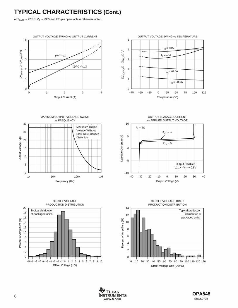
OUTPUT VOLTAGE SWING vs OUTPUT CURRENT
(V+) –VO
(V–) –VO
5
4
3
2
1
0
VS
UP
PLY
–
VO
UT
(V)
Temperature (°C)
OUTPUT VOLTAGE SWING vs TEMPERATURE
–75 –50 –25 0 25 50 75 100 125
IO = +3A
IO = –3A
IO = +0.6A
IO = –0.6A
1k 10k 100k 1M
30
25
20
15
10
5
0
Out
put V
olta
ge (
Vp)
Frequency (Hz)
MAXIMUM OUTPUT VOLTAGE SWINGvs FREQUENCY
Maximum OutputVoltage WithoutSlew Rate InducedDistortion
OFFSET VOLTAGEPRODUCTION DISTRIBUTION
Per
cent
of A
mpl
ifier
s (%
)
Offset Voltage (mV)–10 –9 –8 –7 –6 –5 –4 –3 –2 –1 0 1 2 3 4 5 6 7 8 9 10
20
18
16
14
12
10
8
6
4
2
0
Typical distributionof packaged units.
OFFSET VOLTAGE DRIFTPRODUCTION DISTRIBUTION
Per
cent
of A
mpl
ifier
s (%
)
Offset Voltage Drift (µV/°C)
14
12
10
8
6
4
2
0
Typical productiondistribution of
packaged units.
0 10 20 30 40 50 60 70 80 90 100 110 120 130
–40 –30 –20 –10 0 10 20 4030
10
5
0
–5
–10
Leak
age
Cur
rent
(m
A)
Output Voltage (V)
OUTPUT LEAKAGE CURRENTvs APPLIED OUTPUT VOLTAGE
RL = 8Ω
Output DisabledVE/S < (V–) + 0.8V
RCL = ∞
RCL = 0

OPA548 7SBOS070B www.ti.com
TYPICAL CHARACTERISTICS (Cont.)At TCASE = +25°C, VS = ±30V and E/S pin open, unless otherwise noted.
0 2k 4k 6k 8k 10k 12k 14k 16k 18k 20k
50
40
30
20
10
0
Ove
rsho
ot (
%)
Load Capacitance (pF)
SMALL-SIGNAL OVERSHOOTvs LOAD CAPACITANCE
G = –1
G = +1
SMALL-SIGNAL STEP RESPONSEG = 3, CL = 1000pF
100m
V/d
iv
2µs/div
LARGE-SIGNAL STEP RESPONSEG = 3, CL = 1000pF, RL = 8Ω
10V
/div
5µs/div
SMALL-SIGNAL STEP RESPONSEG = 1, CL = 1000pF
50m
V/d
iv
2µs/div
OPA5488SBOS070Bwww.ti.com
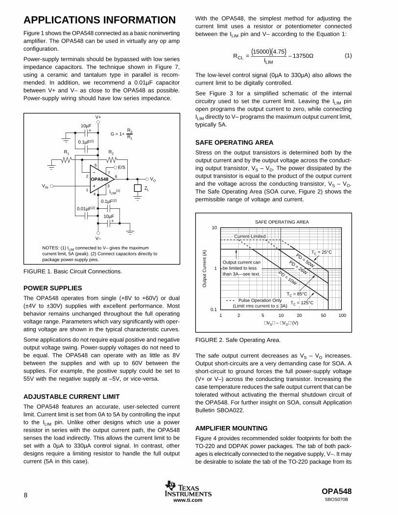
APPLICATIONS INFORMATIONFigure 1 shows the OPA548 connected as a basic noninvertingamplifier. The OPA548 can be used in virtually any op ampconfiguration.
Power-supply terminals should be bypassed with low seriesimpedance capacitors. The technique shown in Figure 7,using a ceramic and tantalum type in parallel is recom-mended. In addition, we recommend a 0.01µF capacitorbetween V+ and V– as close to the OPA548 as possible.Power-supply wiring should have low series impedance.
With the OPA548, the simplest method for adjusting thecurrent limit uses a resistor or potentiometer connectedbetween the ILIM pin and V– according to the Equation 1:
RICLLIM
=( )( )15000 4 75
13750.
– Ω
The low-level control signal (0µA to 330µA) also allows thecurrent limit to be digitally controlled.
See Figure 3 for a simplified schematic of the internalcircuitry used to set the current limit. Leaving the ILIM pinopen programs the output current to zero, while connectingILIM directly to V– programs the maximum output current limit,typically 5A.
SAFE OPERATING AREA
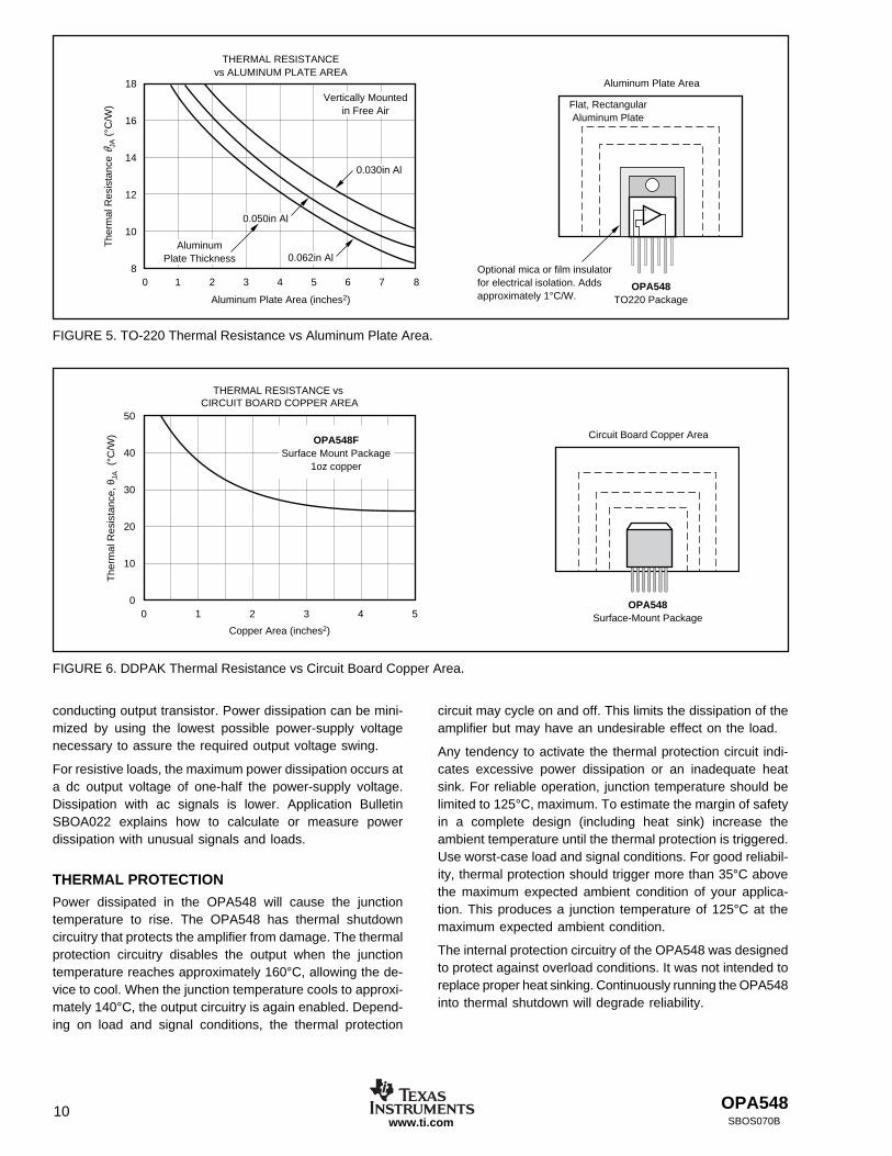
Stress on the output transistors is determined both by theoutput current and by the output voltage across the conduct-ing output transistor, VS – VO. The power dissipated by theoutput transistor is equal to the product of the output currentand the voltage across the conducting transistor, VS – VO.The Safe Operating Area (SOA curve, Figure 2) shows thepermissible range of voltage and current.
FIGURE 1. Basic Circuit Connections.
POWER SUPPLIES
The OPA548 operates from single (+8V to +60V) or dual(±4V to ±30V) supplies with excellent performance. Mostbehavior remains unchanged throughout the full operatingvoltage range. Parameters which vary significantly with oper-ating voltage are shown in the typical characteristic curves.
Some applications do not require equal positive and negativeoutput voltage swing. Power-supply voltages do not need tobe equal. The OPA548 can operate with as little as 8Vbetween the supplies and with up to 60V between thesupplies. For example, the positive supply could be set to55V with the negative supply at –5V, or vice-versa.
ADJUSTABLE CURRENT LIMIT
The OPA548 features an accurate, user-selected currentlimit. Current limit is set from 0A to 5A by controlling the inputto the ILIM pin. Unlike other designs which use a powerresistor in series with the output current path, the OPA548senses the load indirectly. This allows the current limit to beset with a 0µA to 330µA control signal. In contrast, otherdesigns require a limiting resistor to handle the full outputcurrent (5A in this case).
FIGURE 2. Safe Operating Area.
The safe output current decreases as VS – VO increases.Output short-circuits are a very demanding case for SOA. Ashort-circuit to ground forces the full power-supply voltage(V+ or V–) across the conducting transistor. Increasing thecase temperature reduces the safe output current that can betolerated without activating the thermal shutdown circuit ofthe OPA548. For further insight on SOA, consult ApplicationBulletin SBOA022.
AMPLIFIER MOUNTING
Figure 4 provides recommended solder footprints for both theTO-220 and DDPAK power packages. The tab of both pack-ages is electrically connected to the negative supply, V–. It maybe desirable to isolate the tab of the TO-220 package from its
G = 1+ R2
R1
ZL
E/S
3
7
5
2
14
6
R2
ILIM(1)
R1
0.1µF(2)
10µF
OPA548
V–
V+
+
+
VIN
10µF
0.1µF(2)
0.01µF(2)
VO
NOTES: (1) ILIM connected to V– gives the maximum current limit, 5A (peak). (2) Connect capacitors directly to package power-supply pins.
1 2 5 10
VS – VO (V)
20 50 100
SAFE OPERATING AREA10
1
Out
put C
urre
nt (
A)
0.1
Pulse Operation Only(Limit rms current to ≤ 3A)
Current-Limited
Output current canbe limited to lessthan 3A—see text.
TC = 125°C
TC = 85°C
TC = 25°CPD = 50WPD = 26WPD = 10W
(1)

OPA548 9SBOS070B www.ti.com
DDPAK-7(1)
(Package Designator KTW)TO220-7
(Package Designator KVT)
NOTE: (1) For improved thermal performance increase footprint area.See Figure 6, “Thermal Resistance vs Circuit Board Copper Area”.
Mean dimensions in inches. Refer to end of data sheetor www.ti.com for tolerances and detailed packagedrawings.
0.33
5
0.15
0.05
0.45
0.51
0.1050.05
0.035
0.04
0.2
0.08
5
heat dissipation. See Figure 6 for typical thermal resistancefrom junction-to-ambient as a function of the copper area.
POWER DISSIPATION
Power dissipation depends on power supply, signal, and loadconditions. For dc signals, power dissipation is equal tothe product of output current times the voltage across the
mounting surface with a mica (or other film) insulator (seeFigure 5). For lowest overall thermal resistance it is best toisolate the entire heat sink/OPA548 structure from the mount-ing surface rather than to use an insulator between thesemiconductor and heat sink.
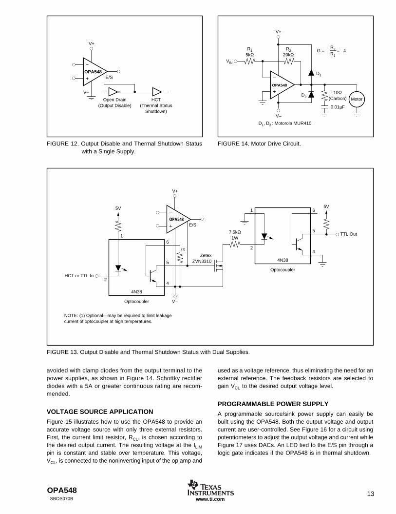
For best thermal performance, the tab of the DDPAK sur-face-mount version should be soldered directly to a circuitboard copper area. Increasing the copper area improves
13750Ω
RCL 0.01µF(optional, for noisyenvironments)
3
4
3
4
4.75V
RCL = – 13750Ω
OPA547 CURRENT LIMIT: 0 to 5A
NOTE: (1) Resistors are nearest standard 1% values.
DESIREDCURRENT LIMIT
0A1A
2.5A3A4A5A
RESISTOR(1)
(RCL)
ILIM Open57.6kΩ14.7kΩ10kΩ
4.02kΩILIM Connected to V–
CURRENT(ISET)
0µA67µA167µA200µA267µA333µA
VOLTAGE(VSET)
(V–) + 4.75V(V–) + 3.8V(V–) + 2.5V(V–) + 2V
(V–) + 1.1V(V–)
RESISTOR METHOD
15000 (4.75V)
ILIM
V–
13750Ω
ISET = ILIM /15000
VSET = (V–) + 4.75V – (13750Ω) (ILIM)/15000
DAC METHOD (Current or Voltage)
V–
D/A
ISET
4.75V
±ILIM =
Max IO = ILIM
(4.75) (15000)
13750Ω + RCL
Max IO = ILIM
±ILIM =15000 ISET
FIGURE 3. Adjustable Current Limit.
FIGURE 4. TO-220 and DDPAK Solder Footprints.
OPA54810SBOS070Bwww.ti.com
THERMAL RESISTANCE vs CIRCUIT BOARD COPPER AREA
50
40
30
20
10
0
The
rmal
Res
ista
nce,
θJA
(°C
/W)
0 1 2 3 4 5
Copper Area (inches2)
OPA548FSurface Mount Package
1oz copper
Circuit Board Copper Area
OPA548Surface-Mount Package
FIGURE 5. TO-220 Thermal Resistance vs Aluminum Plate Area.
FIGURE 6. DDPAK Thermal Resistance vs Circuit Board Copper Area.
conducting output transistor. Power dissipation can be mini-mized by using the lowest possible power-supply voltagenecessary to assure the required output voltage swing.
For resistive loads, the maximum power dissipation occurs ata dc output voltage of one-half the power-supply voltage.Dissipation with ac signals is lower. Application BulletinSBOA022 explains how to calculate or measure powerdissipation with unusual signals and loads.
THERMAL PROTECTION
Power dissipated in the OPA548 will cause the junctiontemperature to rise. The OPA548 has thermal shutdowncircuitry that protects the amplifier from damage. The thermalprotection circuitry disables the output when the junctiontemperature reaches approximately 160°C, allowing the de-vice to cool. When the junction temperature cools to approxi-mately 140°C, the output circuitry is again enabled. Depend-ing on load and signal conditions, the thermal protection
circuit may cycle on and off. This limits the dissipation of theamplifier but may have an undesirable effect on the load.
Any tendency to activate the thermal protection circuit indi-cates excessive power dissipation or an inadequate heatsink. For reliable operation, junction temperature should belimited to 125°C, maximum. To estimate the margin of safetyin a complete design (including heat sink) increase theambient temperature until the thermal protection is triggered.Use worst-case load and signal conditions. For good reliabil-ity, thermal protection should trigger more than 35°C abovethe maximum expected ambient condition of your applica-tion. This produces a junction temperature of 125°C at themaximum expected ambient condition.
The internal protection circuitry of the OPA548 was designedto protect against overload conditions. It was not intended toreplace proper heat sinking. Continuously running the OPA548into thermal shutdown will degrade reliability.
0 1 2 3 4 5 6 7 8
18
16
14
12
10
8
The
rmal
Res
ista
nce
JA (
°C/W
)
Aluminum Plate Area (inches2)
THERMAL RESISTANCEvs ALUMINUM PLATE AREA
Aluminum Plate Area
Flat, RectangularAluminum Plate
OPA548TO220 Package
θ
0.030in Al
0.062in Al
0.050in Al
Vertically Mountedin Free Air
Optional mica or film insulatorfor electrical isolation. Addsapproximately 1°C/W.
AluminumPlate Thickness

OPA548 11SBOS070B www.ti.com
HEAT SINKING
Most applications require a heat sink to assure that themaximum operating junction temperature (125°C) is notexceeded. In addition, the junction temperature should bekept as low as possible for increased reliability. Junctiontemperature can be determined according to the equation:
TJ = TA + PDθJA (1)
where, θJA = θJC + θCH + θHA (2)
TJ = Junction Temperature (°C)TA = Ambient Temperature (°C)PD = Power Dissipated (W)θJC = Junction-to-Case Thermal Resistance (°C/W)θCH = Case-to-Heat Sink Thermal Resistance (°C/W)θHA = Heat Sink-to-Ambient Thermal Resistance (°C/W)θJA = Junction-to-Air Thermal Resistance (°C/W)
Figure 7 shows maximum power dissipation versus ambienttemperature with and without the use of a heat sink. Using aheat sink significantly increases the maximum power dissipa-tion at a given ambient temperature as shown.
The difficulty in selecting the heat sink required lies indetermining the power dissipated by the OPA548. For dcoutput into a purely resistive load, power dissipation is simplythe load current times the voltage developed across theconducting output transistor, PD = IL(VS–VO). Other loads arenot as simple. Consult Application Bulletin SBOA022 forfurther insight on calculating power dissipation. Once powerdissipation for an application is known, the proper heat sinkcan be selected.
Combining equations (1) and (2) gives:
TJ = TA + PD(θJC + θCH + θHA) (3)
TJ, TA, and PD are given. θJC is provided in the specificationtable, 2.5°C/W (dc). θCH can be obtained from the heat sinkmanufacturer. Its value depends on heat sink size, area, andmaterial used. Semiconductor package type, mounting screwtorque, insulating material used (if any), and thermaljoint compound used (if any) also affect θCH. A typical θCH fora TO-220 mounted package is 1°C/W. Now we can solve forθHA:
θ θ θ
θ
HAJ A
DJC CH
HA
T TP
C CW
C W C W C W
= +( )
= ° ° ° + °( ) = °
––
–– . / / . /
125 405
2 5 1 13 5
To maintain junction temperature below 125°C, the heat sinkselected must have a θHA less than 14°C/W. In other words,the heat sink temperature rise above ambient must be lessthan 67.5°C (13.5°C/W • 5W). For example, at 5W Thermalloymodel number 6030B has a heat sink temperature rise of66°C above ambient (θHA = 66°C/5W = 13.2°C/W), which isbelow the 67.5°C required in this example. Figure 7 showspower dissipation versus ambient temperature for a TO-220package with a 6030B heat sink.
Another variable to consider is natural convection versusforced convection air flow. Forced-air cooling by a small fancan lower θCA (θCH + θHA) dramatically. Heat sink manufac-tures provide thermal data for both of these cases. Foradditional information on determining heat sink requirements,consult Application Bulletin SBOA021.
As mentioned earlier, once a heat sink has been selected,the complete design should be tested under worst-case loadand signal conditions to ensure proper thermal protection.
ENABLE/STATUS (E/S) PIN
The Enable/Status pin provides two functions: forcing this pinLOW disables the output stage, or E/S can be monitored todetermine if the OPA548 is in thermal shutdown. One or bothof these functions can be utilized on the same device usingsingle or dual supplies. For normal operation (output en-abled), the E/S pin can be left open or pulled HIGH (at least2.4V above the negative rail). A small value capacitor con-nected between the E/S pin and V– may be required for noisyapplications.
Output DisableA unique feature of the OPA548 is its output disable capabil-ity. This function not only conserves power during idle peri-ods (quiescent current drops to approximately 6mA), but alsoallows multiplexing in low frequency (f < 20kHz), multichan-nel applications. Signals greater than 20kHz may causeleakage current to increase in devices that are shutdown.Figure 18 shows the two OPA548s in a switched amplifierconfiguration. The on/off state of the two amplifiers is con-trolled by the voltage on the E/S pin.
Heat Sink Selection Example
A TO-220 package is dissipating 5W. The maximum ex-pected ambient temperature is 40°C. Find the proper heatsink to keep the junction temperature below 125°C (150°Cminus 25°C safety margin).
FIGURE 7. Maximum Power Dissipation vs AmbientTemperature.
10
8
6
4
2
0
Pow
er D
issi
patio
n (W
atts
)
0 25 50 75 100 125
Ambient Temperature (°C)
MAXIMUM POWER DISSIPATIONvs AMBIENT TEMPERATURE
TO220 with Thermalloy6030B Heat Sink JA = 16.7°C/W
PD = (TJ (max) – TA) / JATJ (max) = 150°C
With infinite heat sink( JA = 2.5°C/W),
max PD = 50W at TA = 25°C.
θ
θ
DDPAK
JA = 26°C/W(3 in2 one ozcopper mounting pad)
θ
DDPAK or TO-220
JA = 65°C/W (no heat sink)θ
θ

OPA54812SBOS070Bwww.ti.com
To disable the output, the E/S pin is pulled LOW, no greaterthan 0.8V above the negative rail. Typically the output isshutdown in 1µs. Figure 8 provides an example of how toimplement this function using a single supply. Figure 9 givesa circuit for dual-supply applications. To return the output to anenabled state, the E/S pin should be disconnected (open) orpulled to at least (V–) + 2.4V. It should be noted that pulling theE/S pin HIGH (output enabled) does not disable internalthermal shutdown.
Output Disable and Thermal Shutdown StatusAs mentioned earlier, the OPA548’s output can be disabledand the disable status can be monitored simultaneously.Figures 12 and 13 provide examples interfacing to the E/Spin while using a single supply and dual supplies, respec-tively.
OUTPUT STAGE COMPENSATION
The complex load impedances common in power op ampapplications can cause output stage instability. For normaloperation output compensation circuitry is typically not re-quired. However, if the OPA548 is intended to be driven intocurrent limit, an R/C network may be required. See Figure 14for an output series R/C compensation (snubber) networkwhich generally provides excellent stability.
A snubber circuit may also enhance stability when drivinglarge capacitive loads (> 1000pF) or inductive loads (motors,loads separated from the amplifier by long cables). Typically3Ω to 10Ω in series with 0.01µF to 0.1µF is adequate. Somevariations in circuit value may be required with certain loads.
OUTPUT PROTECTION
Reactive and EMF-generating loads can return load cur-rent to the amplifier, causing the output voltage to exceedthe power-supply voltage. This damaging condition can be
FIGURE 11. Thermal Shutdown Status with Dual Supplies.
FIGURE 10. Thermal Shutdown Status with a Single Supply.
OPA548
V+
E/S
V–
1kΩ
5V
22kΩ
470Ω
2N3906
ZetexZVN3310
OPA548
V+
E/S
V–
CMOS or TTL
OPA548
V+
E/S
HCT
OR
TTL
2.49kΩ
ZetexZVN3310
5V
V–
Thermal Shutdown StatusInternal thermal shutdown circuitry shuts down the output whenthe die temperature reaches approximately 160°C, resettingwhen the die has cooled to 140°C. The E/S pin can bemonitored to determine if shutdown has occurred. Duringnormal operation the voltage on the E/S pin is typically 3.5Vabove the negative rail. Once shutdown has occurred, thisvoltage drops to approximately 350mV above the negative rail.
Figure 10 gives an example of monitoring shutdown in asingle-supply application. Figure 11 provides a circuit for dualsupplies. External logic circuitry or an LED could be used toindicate if the output has been thermally shutdown, seeFigure 16.
FIGURE 9. Output Disable with Dual Supplies.
OPA548
V+
E/S
V–
NOTE: (1) Optional—may be required to limit leakagecurrent of optocoupler at high temperatures.
(1)
61
1
4N38
Optocoupler
5
4
HCT or TTL In
5V
FIGURE 8. Output Disable with a Single Supply.
OPA548 13SBOS070B www.ti.com
avoided with clamp diodes from the output terminal to thepower supplies, as shown in Figure 14. Schottky rectifierdiodes with a 5A or greater continuous rating are recom-mended.
VOLTAGE SOURCE APPLICATION
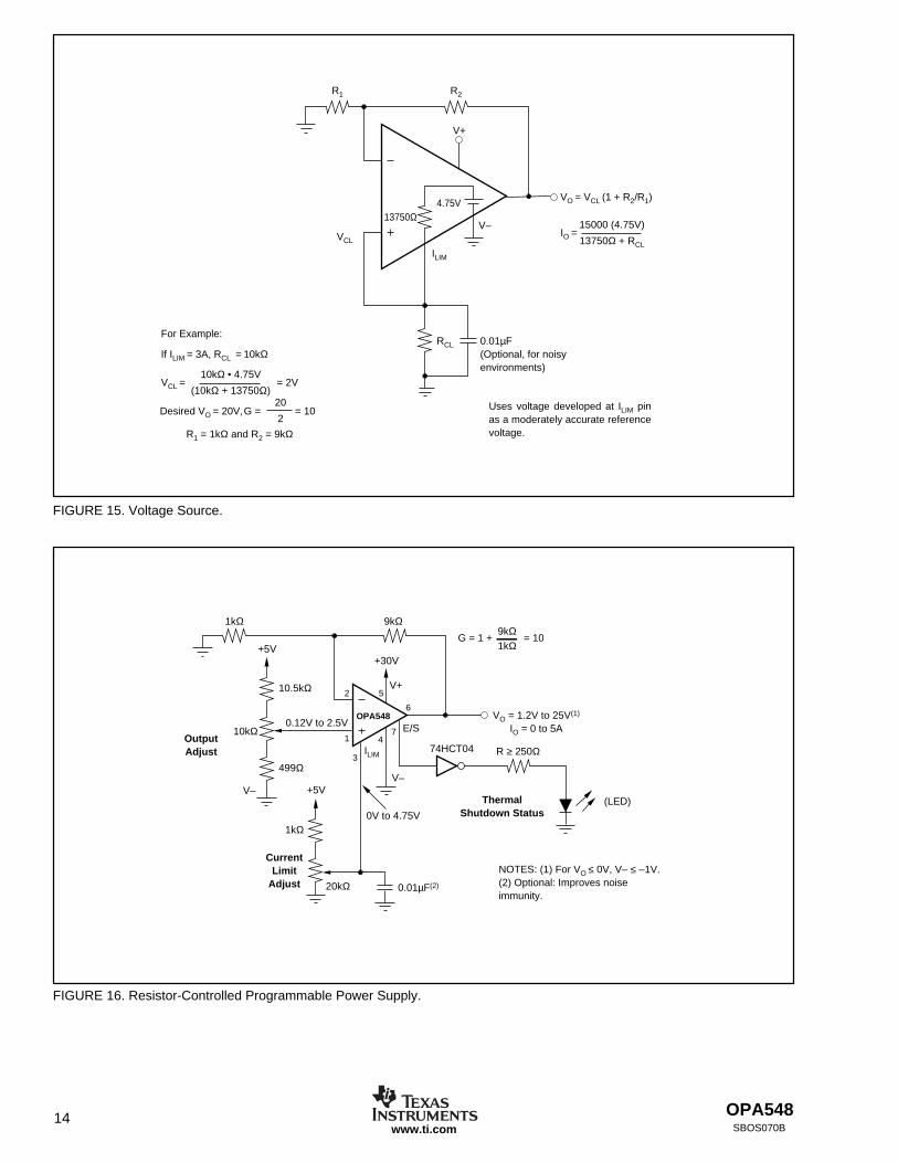
Figure 15 illustrates how to use the OPA548 to provide anaccurate voltage source with only three external resistors.First, the current limit resistor, RCL, is chosen according tothe desired output current. The resulting voltage at the ILIM
pin is constant and stable over temperature. This voltage,VCL, is connected to the noninverting input of the op amp and
used as a voltage reference, thus eliminating the need for anexternal reference. The feedback resistors are selected togain VCL to the desired output voltage level.
PROGRAMMABLE POWER SUPPLY
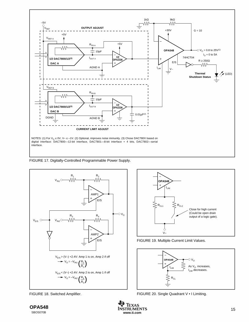
A programmable source/sink power supply can easily bebuilt using the OPA548. Both the output voltage and outputcurrent are user-controlled. See Figure 16 for a circuit usingpotentiometers to adjust the output voltage and current whileFigure 17 uses DACs. An LED tied to the E/S pin through alogic gate indicates if the OPA548 is in thermal shutdown.
FIGURE 13. Output Disable and Thermal Shutdown Status with Dual Supplies.
FIGURE 12. Output Disable and Thermal Shutdown Statuswith a Single Supply.
FIGURE 14. Motor Drive Circuit.
OPA548
V+
E/S
Open Drain(Output Disable)
HCT(Thermal Status
Shutdown)
V–
OPA548
V+
E/S
NOTE: (1) Optional—may be required to limit leakagecurrent of optocoupler at high temperatures.
V–
(1)
61
2
4N38
Optocoupler
5
4
HCT or TTL In
5V 6
2
1
4N38
Optocoupler
5
4Zetex
ZVN3310
TTL Out7.5kΩ1W
5V
G = – = –4R2
R1
10Ω(Carbon)
0.01µF
R220kΩ
R15kΩ
OPA548
V–
V+
VIN
Motor
D1
D2
D1, D2 : Motorola MUR410.
OPA54814SBOS070Bwww.ti.com
G = 1 + = 109kΩ1kΩ
9kΩ1kΩ
OPA548
+30V+5V
+5V
0.12V to 2.5V
0V to 4.75V
OutputAdjust
V+5
6
ThermalShutdown Status
NOTES: (1) For VO ≤ 0V, V– ≤ –1V.(2) Optional: Improves noiseimmunity.
(LED)
74HCT04 R ≥ 250Ω
E/SVO = 1.2V to 25V(1)
IO = 0 to 5A74
3
1
2
V–
ILIM
10.5kΩ
499Ω
10kΩ
CurrentLimit
Adjust
1kΩ
20kΩ 0.01µF(2)
V–
13750Ω
RCL
ILIM
0.01µF(Optional, for noisyenvironments)
4.75V
IO =15000 (4.75V)
13750Ω + RCL
VO = VCL (1 + R2/R1)
V–
V+
VCL
VCL = = 2V
Desired VO = 20V,
R1 = 1kΩ and R2 = 9kΩ
G = = 1020
2
For Example:
10kΩ • 4.75V
(10kΩ + 13750Ω)
If ILIM = 3A, RCL = 10kΩ
R2R1
Uses voltage developed at ILIM pin as a moderately accurate reference voltage.
FIGURE 16. Resistor-Controlled Programmable Power Supply.
FIGURE 15. Voltage Source.
OPA548 15SBOS070B www.ti.com
( )
E/S
R2R1
VIN1
AMP1
VO
E/S
R4R3
VE/S > (V–) +2.4V: Amp 1 is on, Amp 2 if off
VO = –VIN1 R2
R1
VE/S VIN2
AMP2
( )VE/S < (V–) +2.4V: Amp 2 is on, Amp 1 if off
VO = –VIN2 R4
R3
OPA548
RCL2RCL1
Close for high current(Could be open drainoutput of a logic gate).
ILIM
V–
FIGURE 19. Multiple Current Limit Values.
FIGURE 20. Single Quadrant V • I Limiting.
FIGURE 17. Digitally-Controlled Programmable Power Supply.
OPA548 VO
ILIM
RCL
As VO increases,ILIM decreases.
FIGURE 18. Switched Amplifier.
DAC B
1/2 DAC7800/1/2(3)
1/2 DAC7800/1/2(3)
10pF
IOUT B
RFB B
AGND B0.01µF(2)
ILIM
ThermalShutdown Status
(LED)
74HCT04R ≥ 250Ω
9kΩ1kΩ
VO = 0.8 to 25V(1)
IO = 0 to 5A
G = 10
V–
E/SDAC A
+5V
+5V
VREF B
DGND
10pF
IOUT A
RFB A
OUTPUT ADJUST
OPA548
CURRENT LIMIT ADJUST
AGND A
+30V
VREF A
NOTES: (1) For VO ≤ 0V, V– ≤ –1V. (2) Optional, improves noise immunity. (3) Chose DAC780X based on digital interface: DAC7800—12-bit interface, DAC7801—8-bit interface + 4 bits, DAC7802—serial interface.
1/2OPA2336
1/2OPA2336
VREF
–5V
OPA54816SBOS070Bwww.ti.com
ILIM
V–
V+
R11kΩ
R24kΩ
OPA548
OPA548
VOIO = 10A (peak)(2)
G = 1 + = 5(1)
VIN
800Ω
800Ω
0.25Ω4kΩ1kΩ
0.25Ω
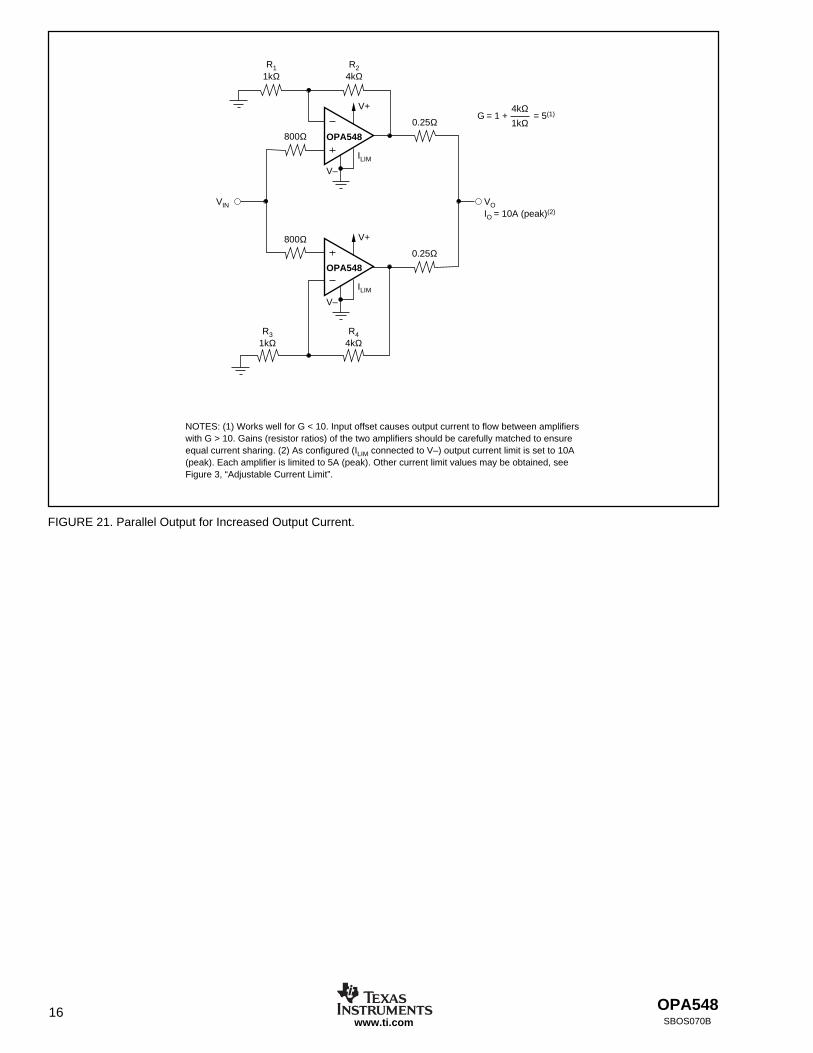
NOTES: (1) Works well for G < 10. Input offset causes output current to flow between amplifiers with G > 10. Gains (resistor ratios) of the two amplifiers should be carefully matched to ensure equal current sharing. (2) As configured (ILIM connected to V–) output current limit is set to 10A (peak). Each amplifier is limited to 5A (peak). Other current limit values may be obtained, see Figure 3, “Adjustable Current Limit”.
ILIM
V–
V+
R31kΩ
R44kΩ
FIGURE 21. Parallel Output for Increased Output Current.

PACKAGING INFORMATION
Orderable Device Status (1) PackageType
PackageDrawing
Pins PackageQty
Eco Plan (2) Lead/Ball Finish MSL Peak Temp (3)
OPA548F OBSOLETE DDPAK KTW 7 TBD Call TI Call TI
OPA548F/500 ACTIVE DDPAK KTW 7 500 Green (RoHS &no Sb/Br)
CU SN Level-2-260C-1 YEAR
OPA548F/500G3 ACTIVE DDPAK KTW 7 500 Green (RoHS &no Sb/Br)
CU SN Level-2-260C-1 YEAR
OPA548FKTWT ACTIVE DDPAK KTW 7 50 Green (RoHS &no Sb/Br)
CU SN Level-2-260C-1 YEAR
OPA548FKTWTG3 ACTIVE DDPAK KTW 7 50 Green (RoHS &no Sb/Br)
CU SN Level-2-260C-1 YEAR
OPA548T ACTIVE TO-220 KVT 7 50 Green (RoHS &no Sb/Br)
CU SN N / A for Pkg Type
OPA548T-1 ACTIVE TO-220 KC 7 50 Green (RoHS &no Sb/Br)
CU SN N / A for Pkg Type
OPA548T-1G3 ACTIVE TO-220 KC 7 50 Green (RoHS &no Sb/Br)
CU SN N / A for Pkg Type
OPA548TG3 ACTIVE TO-220 KVT 7 50 Green (RoHS &no Sb/Br)
CU SN N / A for Pkg Type
(1) The marketing status values are defined as follows:ACTIVE: Product device recommended for new designs.LIFEBUY: TI has announced that the device will be discontinued, and a lifetime-buy period is in effect.NRND: Not recommended for new designs. Device is in production to support existing customers, but TI does not recommend using this part ina new design.PREVIEW: Device has been announced but is not in production. Samples may or may not be available.OBSOLETE: TI has discontinued the production of the device.
(2) Eco Plan - The planned eco-friendly classification: Pb-Free (RoHS), Pb-Free (RoHS Exempt), or Green (RoHS & no Sb/Br) - please checkhttp://www.ti.com/productcontent for the latest availability information and additional product content details.TBD: The Pb-Free/Green conversion plan has not been defined.Pb-Free (RoHS): TI's terms "Lead-Free" or "Pb-Free" mean semiconductor products that are compatible with the current RoHS requirementsfor all 6 substances, including the requirement that lead not exceed 0.1% by weight in homogeneous materials. Where designed to be solderedat high temperatures, TI Pb-Free products are suitable for use in specified lead-free processes.Pb-Free (RoHS Exempt): This component has a RoHS exemption for either 1) lead-based flip-chip solder bumps used between the die andpackage, or 2) lead-based die adhesive used between the die and leadframe. The component is otherwise considered Pb-Free (RoHScompatible) as defined above.Green (RoHS & no Sb/Br): TI defines "Green" to mean Pb-Free (RoHS compatible), and free of Bromine (Br) and Antimony (Sb) based flameretardants (Br or Sb do not exceed 0.1% by weight in homogeneous material)
(3) MSL, Peak Temp. -- The Moisture Sensitivity Level rating according to the JEDEC industry standard classifications, and peak soldertemperature.
Important Information and Disclaimer:The information provided on this page represents TI's knowledge and belief as of the date that it isprovided. TI bases its knowledge and belief on information provided by third parties, and makes no representation or warranty as to theaccuracy of such information. Efforts are underway to better integrate information from third parties. TI has taken and continues to takereasonable steps to provide representative and accurate information but may not have conducted destructive testing or chemical analysis onincoming materials and chemicals. TI and TI suppliers consider certain information to be proprietary, and thus CAS numbers and other limitedinformation may not be available for release.
In no event shall TI's liability arising out of such information exceed the total purchase price of the TI part(s) at issue in this document sold by TIto Customer on an annual basis.
PACKAGE OPTION ADDENDUM
www.ti.com 18-Sep-2008
Addendum-Page 1
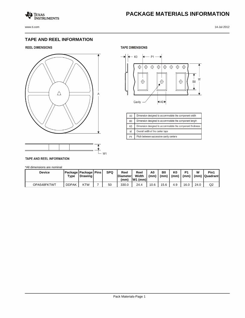
TAPE AND REEL INFORMATION
*All dimensions are nominal
Device PackageType
PackageDrawing
Pins SPQ ReelDiameter
(mm)
ReelWidth
W1 (mm)
A0(mm)
B0(mm)
K0(mm)
P1(mm)
W(mm)
Pin1Quadrant
OPA548FKTWT DDPAK KTW 7 50 330.0 24.4 10.6 15.6 4.9 16.0 24.0 Q2
PACKAGE MATERIALS INFORMATION
www.ti.com 14-Jul-2012
Pack Materials-Page 1

*All dimensions are nominal
Device Package Type Package Drawing Pins SPQ Length (mm) Width (mm) Height (mm)
OPA548FKTWT DDPAK KTW 7 50 367.0 367.0 45.0
PACKAGE MATERIALS INFORMATION
www.ti.com 14-Jul-2012
Pack Materials-Page 2

MECHANICAL DATA
MPSF015 – AUGUST 2001
POST OFFICE BOX 655303 • DALLAS, TEXAS 75265
KTW (R-PSFM-G7) PLASTIC FLANGE-MOUNT
0.010 (0,25) A M
4201284/A 08/01
0.385 (9,78)0.410 (10,41)
M MB C
–A–0.006
–B–
0.170 (4,32)
0.183 (4,65)
0.000 (0,00)
0.012 (0,305)
0.104 (2,64)0.096 (2,44)
0.034 (0,86)0.022 (0,57)
0.050 (1,27)
0.055 (1,40)
0.045 (1,14)
0.014 (0,36)0.026 (0,66)
0.330 (8,38)
0.370 (9,40)
0.297 (7,54)0.303 (7,70)
0.0585 (1,485)
0.0625 (1,587)
0.595 (15,11)
0.605 (15,37)
0.019 (0,48)
0.017 (0,43)
0°~3°
0.179 (4,55)
0.187 (4,75)
0.056 (1,42)
0.064 (1,63)
0.296 (7,52)
0.304 (7,72)
0.300 (7,62)
0.252 (6,40)
F
C
C
H
H
H
C
A
NOTES: A. All linear dimensions are in inches (millimeters).B. This drawing is subject to change without notice.
C. Lead width and height dimensions apply to theplated lead.
D. Leads are not allowed above the Datum B.E. Stand–off height is measured from lead tip
with reference to Datum B.F. Lead width dimension does not include dambar
protrusion. Allowable dambar protrusion shall notcause the lead width to exceed the maximumdimension by more than 0.003”.
G. Cross–hatch indicates exposed metal surface.
H. Falls within JEDEC MO–169 with the exceptionof the dimensions indicated.

MECHANICAL DATA
MSOT010 – OCTOBER 1994
1POST OFFICE BOX 655303 • DALLAS, TEXAS 75265
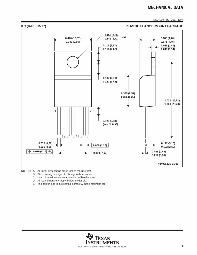
KC (R-PSFM-T7) PLASTIC FLANGE-MOUNT PACKAGE
4040251/B 01/95
0.420 (10,67)
0.055 (1,40)
0.335 (8,51)
0.030 (0,76)0.026 (0,66)
0.380 (9,65)
0.325 (8,25)
0.045 (1,14)0.113 (2,87)0.103 (2,62)
0.146 (3,71)0.156 (3,96)
0.122 (3,10)0.102 (2,59)
DIA
(see Note C)0.125 (3,18)
0.137 (3,48)0.147 (3,73)
1.020 (25,91)1.000 (25,40)
0.175 (4,46)0.185 (4,70)
1 7
0.050 (1,27)
0.300 (7,62) 0.025 (0,64)0.012 (0,30)
M0.010 (0,25)
NOTES: A. All linear dimensions are in inches (millimeters).B. This drawing is subject to change without notice.C. Lead dimensions are not controlled within this area.D. All lead dimensions apply before solder dip.E. The center lead is in electrical contact with the mounting tab.

IMPORTANT NOTICE
Texas Instruments Incorporated and its subsidiaries (TI) reserve the right to make corrections, enhancements, improvements and otherchanges to its semiconductor products and services per JESD46C and to discontinue any product or service per JESD48B. Buyers shouldobtain the latest relevant information before placing orders and should verify that such information is current and complete. Allsemiconductor products (also referred to herein as “components”) are sold subject to TI’s terms and conditions of sale supplied at the timeof order acknowledgment.
TI warrants performance of its components to the specifications applicable at the time of sale, in accordance with the warranty in TI’s termsand conditions of sale of semiconductor products. Testing and other quality control techniques are used to the extent TI deems necessaryto support this warranty. Except where mandated by applicable law, testing of all parameters of each component is not necessarilyperformed.
TI assumes no liability for applications assistance or the design of Buyers’ products. Buyers are responsible for their products andapplications using TI components. To minimize the risks associated with Buyers’ products and applications, Buyers should provideadequate design and operating safeguards.
TI does not warrant or represent that any license, either express or implied, is granted under any patent right, copyright, mask work right, orother intellectual property right relating to any combination, machine, or process in which TI components or services are used. Informationpublished by TI regarding third-party products or services does not constitute a license to use such products or services or a warranty orendorsement thereof. Use of such information may require a license from a third party under the patents or other intellectual property of thethird party, or a license from TI under the patents or other intellectual property of TI.
Reproduction of significant portions of TI information in TI data books or data sheets is permissible only if reproduction is without alterationand is accompanied by all associated warranties, conditions, limitations, and notices. TI is not responsible or liable for such altereddocumentation. Information of third parties may be subject to additional restrictions.
Resale of TI components or services with statements different from or beyond the parameters stated by TI for that component or servicevoids all express and any implied warranties for the associated TI component or service and is an unfair and deceptive business practice.TI is not responsible or liable for any such statements.
Buyer acknowledges and agrees that it is solely responsible for compliance with all legal, regulatory and safety-related requirementsconcerning its products, and any use of TI components in its applications, notwithstanding any applications-related information or supportthat may be provided by TI. Buyer represents and agrees that it has all the necessary expertise to create and implement safeguards whichanticipate dangerous consequences of failures, monitor failures and their consequences, lessen the likelihood of failures that might causeharm and take appropriate remedial actions. Buyer will fully indemnify TI and its representatives against any damages arising out of the useof any TI components in safety-critical applications.
In some cases, TI components may be promoted specifically to facilitate safety-related applications. With such components, TI’s goal is tohelp enable customers to design and create their own end-product solutions that meet applicable functional safety standards andrequirements. Nonetheless, such components are subject to these terms.
No TI components are authorized for use in FDA Class III (or similar life-critical medical equipment) unless authorized officers of the partieshave executed a special agreement specifically governing such use.
Only those TI components which TI has specifically designated as military grade or “enhanced plastic” are designed and intended for use inmilitary/aerospace applications or environments. Buyer acknowledges and agrees that any military or aerospace use of TI componentswhich have not been so designated is solely at the Buyer's risk, and that Buyer is solely responsible for compliance with all legal andregulatory requirements in connection with such use.
TI has specifically designated certain components which meet ISO/TS16949 requirements, mainly for automotive use. Components whichhave not been so designated are neither designed nor intended for automotive use; and TI will not be responsible for any failure of suchcomponents to meet such requirements.
Products Applications
Audio www.ti.com/audio Automotive and Transportation www.ti.com/automotive
Amplifiers amplifier.ti.com Communications and Telecom www.ti.com/communications
Data Converters dataconverter.ti.com Computers and Peripherals www.ti.com/computers
DLP® Products www.dlp.com Consumer Electronics www.ti.com/consumer-apps
DSP dsp.ti.com Energy and Lighting www.ti.com/energy
Clocks and Timers www.ti.com/clocks Industrial www.ti.com/industrial
Interface interface.ti.com Medical www.ti.com/medical
Logic logic.ti.com Security www.ti.com/security
Power Mgmt power.ti.com Space, Avionics and Defense www.ti.com/space-avionics-defense
Microcontrollers microcontroller.ti.com Video and Imaging www.ti.com/video
RFID www.ti-rfid.com
OMAP Mobile Processors www.ti.com/omap TI E2E Community e2e.ti.com
Wireless Connectivity www.ti.com/wirelessconnectivity
Mailing Address: Texas Instruments, Post Office Box 655303, Dallas, Texas 75265Copyright © 2012, Texas Instruments Incorporated

Mouser Electronics
Authorized Distributor
Click to View Pricing, Inventory, Delivery & Lifecycle Information: Texas Instruments:
OPA548T-1 OPA548F/500 OPA548F/500G3 OPA548FKTWT OPA548FKTWTG3 OPA548T OPA548T-1G3
OPA548TG3