hot carrier solar cells
TRANSCRIPT

Hot Carrier Solar Cells
Modelling of Practical Efficiency and
Characterization of Absorber and
Energy Selective Contacts
Pasquale Aliberti
School of Photovoltaic and Renewable Energy Engineering
ARC Photovoltaics Centre of Excellence
The University of New South Wales
UNSW Sydney NSW 2052
Australia
A thesis submitted to The University of New South Wales
In fulfilment of the requirements for the degree of
Doctor of Philosophy
2011

PLEASE TYPE THE UNIVERSITY OF NEW SOUTH WALES
Thesis/Dissertation Sheet Surname or Family name: Aliberti
First name: Pasquale
Other name/s:
Abbreviation for degree as given in the University calendar:
School: School of Photovoltaics and Renewable Energy Engineering
Faculty: Engineering
Title: Recent Progresses in Hot Carrier Solar Cells
Abstract 350 words maximum: (PLEASE TYPE)
The current increase in the demand for renewable energies has led to a fast growth of solar cells mass production over the past few years. Even though solar photovoltaic is currently the fastest growing renewable energy market, the cost per watt figure is still high compared to conventional energy sources. To decrease the cost per watt ratio of solar cells two basic approaches can be undertaken: the first one is to decrease the cost of the devices, using cheaper deposition techniques and materials; the other is to increase the efficiency of the cells, keeping the costs below an acceptable limit. The hot carrier solar cell is a promising third generation photovoltaic device which, consenting collection of highly energetic photogenerated carriers, allows efficiencies up to 60%. The efficiency gain is realized minimizing the losses due to poor conversion efficiency of photons with energy above the bandgap of the absorber. The two main building blocks of a hot carrier solar cell are: the absorber, were electrons and holes are photogenerated, and the energy selective contacts, which allow extraction of carriers to the external circuit in a narrow range of energies. In this thesis several theoretical and experimental aspects regarding the design and the realization of a hot carrier solar cell are discussed. Limiting efficiencies of the device have been calculated using a complex theoretical model. A maximum efficiency of 43% has been calculated considering a 1000 times concentrated radiation for a hot carrier solar cell with an Indium Nitride absorber. The velocity of carrier cooling in III-V compound semiconductors has been investigated using time resolved photoluminescence experiments. Hot carrier cooling transients of Gallium Arsenide, Indium Phosphide and Indium Nitride samples have been studied, confirming that hot phonon effect has a major role for hot carriers relaxation. In addition, the possibility of realizing energy selective contacts based on an all-Silicon structure is studied. Structures consisting of a single layer of Silicon quantum dots in a Silicon dioxide matrix have been deposited and characterized in order to investigate on their potential to be utilized as energy selective contacts for hot carrier solar cells.
Declaration relating to disposition of project thesis/dissertation I hereby grant to the University of New South Wales or its agents the right to archive and to make available my thesis or dissertation in whole or in part in the University libraries in all forms of media, now or here after known, subject to the provisions of the Copyright Act 1968. I retain all property rights, such as patent rights. I also retain the right to use in future works (such as articles or books) all or part of this thesis or dissertation. I also authorise University Microfilms to use the 350 word abstract of my thesis in Dissertation Abstracts International (this is applicable to doctoral theses only). …………………………………………………………… Signature
……………………………………..……………… Witness
……….……………………...…….… Date
The University recognises that there may be exceptional circumstances requiring restrictions on copying or conditions on use. Requests for restriction for a period of up to 2 years must be made in writing. Requests for a longer period of restriction may be considered in exceptional circumstances and require the approval of the Dean of Graduate Research. FOR OFFICE USE ONLY
Date of completion of requirements for Award:
THIS SHEET IS TO BE GLUED TO THE INSIDE FRONT COVER OF THE THESIS

Originality statement
‘I hereby declare that this submission is my own work and to the best of my
knowledge it contains no materials previously published or written by another
person, nor material which to a substantial extent has been accepted for the
award of any other degree or diploma at UNSW or any other educational
institution, except where due acknowledgment is made in the thesis. Any
contribution made to research by others, with whom I have worked at UNSW or
elsewhere, is explicitly acknowledged in the thesis. I also declare that the
intellectual content of this thesis is the product of my own work, except to the
extent that assistance from others in the project’s design and conception or in
style, presentation and linguistic expression is acknowledged.’
Pasquale Aliberti
March 30, 2011
i

Copyright statement
‘I hereby grant the University of New South Wales or its agents the right to
archive and to make available my thesis or dissertation in whole or in part in
the University libraries in all forms of media, now or here after known, subject
to the provisions of the Copyright Act 1968. I retain all proprietary rights, such
as patent rights. I also retain the right to use in future works (such as articles or
books) all or part of this thesis or dissertation. I also authorise University
Microfilms to use the 350 word abstract of my thesis in Dissertation Abstract
International (this is applicable to doctoral theses only). I have either used no
substantial portions of copyright material in my thesis or I have obtained
permission to use copyright material; where permission has not been granted I
have applied/will apply for a partial restriction of the digital copy of my thesis
or dissertation.’
Pasquale Aliberti
March 30, 2011
ii

Authenticity statement
‘I certify that the Library deposit digital copy is a direct equivalent of the
final officially approved version of my thesis. No emendation of content has
occurred and if there are any minor variations in formatting, they are the result
of the conversion to the digital format.’
Pasquale Aliberti
March 30, 2011
iii

iv
Abstract
The current increase in the demand for renewable energies has led to a fast
growth of solar cells mass production over the past few years. Even though
solar photovoltaic is currently the fastest growing renewable energy market, the
cost per watt figure of solar cells is still high compared to conventional energy
sources.
To decrease the cost per watt ratio of solar cells two basic approaches can be
undertaken: the first one is to decrease the cost of the devices, using cheaper
deposition techniques and materials; the other is to increase the efficiency of
the cells, keeping the costs below an acceptable limit.
The hot carrier solar cell is a promising third generation photovoltaic device
which, consenting collection of highly energetic photogenerated carriers,
allows energy conversion efficiencies up to 60%. The efficiency gain is
realized minimizing the losses due to poor conversion efficiency of photons
with energy above the bandgap of the absorber. This represents the main
energy loss mechanism in conventional solar cells, accounting for about 40
percent of the total losses. The two main building blocks of a hot carrier solar
cell are: the absorber, were electrons and holes are photogenerated, and the
energy selective contacts, which allow extraction of carriers to the external
circuit in a narrow range of energies.
In this thesis several theoretical and experimental aspects regarding the
design and the realization of a hot carrier solar cell are discussed in details.
Limiting efficiencies of the device have been calculated using a complex
theoretical model. A maximum efficiency of 43% has been calculated

v
considering a 1000 times concentrated radiation for a hot carrier solar cell with
an indium nitride absorber.
The velocity of carrier cooling in III-V compound semiconductors has been
investigated using time resolved photoluminescence experiments. Hot carrier
cooling transients of gallium arsenide, indium phosphide and indium nitride
samples have been studied, confirming that the hot phonon effect has a major
role for hot carriers relaxation and that the velocity of the cooling process is
strictly related to material quality.
In addition, the possibility of realizing energy selective contacts based on an
all-silicon structure is studied in details. Structures consisting of a single layer
of silicon quantum dots in a silicon dioxide matrix have been deposited and
characterized in order to investigate their potential to be utilized as selective
energy contacts for hot carrier solar cells.

vi
Alla mia famiglia.
Per essermi stati cosí vicino da tanto
lontano.
Sarete sempre il mio più grande
orgoglio.

vii
Acknowledgments
In the first place I would like to thank my supervisor Professor Gavin
Conibeer for allowing me to work on this challenging and exciting project. I
am grateful for his trust and for the autonomy that he gave me throughout the
entire degree. This allowed me to investigate aspects of the project that
interested me the most, keeping my curiosity always at high levels.
I am also grateful to Dr. Santosh Shrestha for supervising me during the
early stages of my experimental work, for his help with the daily laboratory
challenges and his scientific and moral support throughout the entire duration
of my studies. I would also like to thank my co-supervisor Professor Martin
Green for his precious advices and punctual guidance during crucial moments
of my research. It has been a great honour for me to be one of his students. A
special thank goes to Yu Feng who has been a brilliant student, always curious
and motivated. I appreciated his great help for the computation of numerical
results, presented in the second chapter of this thesis, and the theoretical
discussions on functional aspects of hot carrier solar cells. Precious have also
been discussions and advices of Dr. Dirk König, in particular for the
interpretation of carriers cooling transients, presented in chapter four, and the
relations with intervalley scattering. Thanks to Dr. Yasuhiko Takeda for the
scientific debates on efficiency limits of hot carrier cells and for his support
with the numerical calculations. I am grateful to Dr. Ivan Perez-Wurfl and Dr.
Chris Flynn for their help with processing and characterization, in particular
photolithography and optical measurements. Thanks also to Dr. Raphael Clady
for his great support and patience with our long sessions on the time resolved

viii
photoluminescence setup at Sydney University. Thanks to Murad Tayebjee and
Dr. Tim Schmidt for discussions of results of time resolved experiments.
Thanks to Dr. Shujuan Huang and Dr. Yidan Huang for their help with TEM
and to Dr. Bill Gong for the XPS measurements. Great thanks to Dr. Charlie
Kong, Katie Levick, Sean Lim and all the staff at the UNSW Mark Wainwright
analytical centre for their professional and continuous support. I’m also
thankful to the entire LDOT team of the SPREE for being so efficient in
keeping the laboratories in such an amazing working order, despite of the
enormous number of users that have been trying to break the unbreakable
during these four years.
Thanks to Mr. (soon Dr.) Bo Zhang for being my best desk neighborough
and mandarin teacher, and to Binesh for his revelations on scientific gambling.
I am deeply grateful to my friends, mates and colleagues Yong, Andy and
Rob for discovering the Asian half of my spirit, introducing me to karaoke and
Mahjong and for sharing with me the bright and dark moments of these years.
Making it to the end would have been a much harder job without them. I also
thank my mate and colleague Nino for dragging me to the best live gigs in
town. Thanks to Danny, Julie and the entire staff of the school for their friendly
and punctual help. I am also grateful to all my students of “applied
photovoltaics” and “introduction to electronic devices” for making my teaching
activity at UNSW such a rewarding experience.
I thank my Mum, my Dad and my Brother for being able to love and support
me despite of the 16143 kilometres that separate us. Thanks to my friends back
home Valentina, Michele, Ruben, Antonio and Donato for being so close and so
concerned about my safety in the Australian surf. I will be always grateful to
Maria Teresa for being so patient and helpful during these years. Without her
support it would have been hard to overcome some of the difficult times.
I finally thank the University of New South Wales for awarding me with
such a prestigious scholarship, which allowed me to enjoy this remarkable and
unforgettable time.

ix
‘Imagination is more
important than
knowledge.’
Albert Einstein

x
Contents
1 INTRODUCTION
1.1 Premise 1
1.2 Photovoltaic devices 4
1.3 Hot carrier solar cells 7
1.4 Aim and structure of this thesis 11
1.5 Bibliography 13
2 MODELLING EFFICIENCY LIMITS FOR HOT CARRIERS SOLAR CELLS
2.1 Introduction 16
2.2 Literature Review 19
2.2.1 Landsberg thermodynamic limit 19
2.2.2 Shockley-Queisser approach 21
2.2.3 Ross and Nozik approach for calculation of hot carrier
solar cell efficiency 22
2.2.4 Auger recombination-impact ionization model 24
2.2.5 Introduction of thermalisation time and absorber E-k
relation 26
2.3 Modelling efficiency limit for a hot carrier solar cell with an
indium nitride absorber 28
2.3.1 Model assumptions 28
2.3.2 Modelling of J-V characteristics 29
2.3.3 Carrier density calculation 32
2.3.4 Auger recombination and impact ionization coefficients
calculation 33

xi
2.3.5 Hot carrier solar cell efficiency calculation 35
2.3.6 Variation of conversion efficiency with carriers
extraction energy 36
2.3.7 Hot carrier solar cell operation analysis 37
2.3.8 Calculation of Auger recombination and impact
ionization rates 41
2.3.9 Thermalisation losses and efficiency versus
thermalisation time 42
2.3.10 Efficiency computation with indium nitride absorption
coefficient 44
2.4 Efficiency limit calculation with non ideal energy selective
contacts 47
2.4.1 Theoretical description of non-ideal energy selective
contacts 47
2.4.2 Results of calculation of efficiency limit with non-ideal
energy selective contacts 48
2.5 Summary 51
2.6 Bibliography 53
2.7 Publications 57
3 REALIZATION AND CHARACTERIZATION OF SINGLE LAYER SILICON
QUANTUM DOTS IN SILICON DIOXIDE STRUCTURES FOR ENERGY
SELECTIVE CONTACTS APPLICATIONS
3.1 Introduction 58
3.2 Literature review 60
3.3 Realization of single layer silicon quantum dots structure 64
3.3.1 Initial substrate preparation 64
3.3.2 Sputtering of the silicon rich oxide/silicon dioxide
structure 65
3.3.3 High temperature annealing 67
3.4 Investigation of optical and physical properties of silicon rich
oxides layers and nucleation of silicon nanoparticles 68

xii
3.4.1 Investigation of silicon rich oxide composition 69
3.4.2 Nucleation of silicon quantum dots in silicon rich oxide 74
3.5 Investigation of quantum dots nucleation and quantum
confinement in single layers of silicon quantum dots in silicon
dioxide 79
3.5.1 Quantum confinement effect in single layer quantum
dots structures 79
3.5.2 Study of nucleation process of single layer silicon
quantum dots in Nitrogen annealing atmosphere 84
3.5.3 Effects of forming gas annealing on single layer silicon
quantum dots structures 87
3.5.4 Oxidation of silicon quantum dots in Nitrogen annealing
environment 89
3.6 Summary 91
3.7 Bibliography 93
3.8 Publications 98
4 TIME RESOLVED PHOTOLUMINESCENCE EXPERIMENTS FOR
CHARACTERIZATION OF HOT CARRIER SOLAR CELL ABSORBERS
4.1 Introduction 100
4.2 Literature review 104
4.3 Probing ultrafast dynamic processes in semiconductors 110
4.3.1 Time resolved photoluminescence using up-conversion
technique 110
4.4 Comparison of hot carrier cooling gallium arsenide and
indium phosphide 114
4.4.1 Hot carriers cooling 115
4.4.2 Hot phonon effect in gallium arsenide and indium
phosphide 118
4.4.3 Inter-valley scattering of hot carriers in gallium arsenide
and indium phosphide 122
4.5 TRPL of hot carriers in indium nitride layers 124

xiii
4.5.1 Preliminary results on hot carriers cooling in wurtzite
indium nitride 124
4.6 Summary 129
4.7 Bibliography 131
4.8 Publications 137
5 DISCUSSION
5.1 Introduction 138
5.2 Correlation between important parameters of a hot carrier
solar cell 139
5.3 Considerations on energy selective contacts 142
5.3.1 Additional requirements for energy selective contacts
design 145
5.4 Considerations on absorber materials 147
5.4.1 Bulk semiconductors 147
5.4.2 Nanostructured semiconductors 149
5.5 Possible preliminary design of a hot carrier solar cell 150
5.6 Summary 152
5.7 Bibliography 153
6 CONCLUSIONS


Chapter 1
INTRODUCTION

Chapter 1: Introduction
1.1 Premise
Recent research studies have predicted that the world energy consumption
will increase by 49 percent (1.4 percent / year), from 145 trillion kilowatthours
in 2007, to 216 trillion kilowatthours in 2035 [1].
Figure 1.1.1 – World marketed energy consumption [1]. 1 kWh = 3.6 MJ.
The use of all energy sources is predicted to increase. The access to fossil
fuels, in particular liquid fuels and petroleum, will become more complicated
and expensive, thus the consumption of oil is predicted to grow at a very slow
rate. The growth in coal usage instead is determined by the fast developing rate
of China, which has an energy industry mostly based on coal fired power
plants.
A large increase in energy generation from renewable sources is expected to
meet the increment in energy demand in the next decades. Figure 1.1.2 shows
an increase in the projected renewable energy production from 3.46 trillion
kilowatthours in 2007 to 7.97 trillion kilowatthours in 2035. Currently
hydroelectric and wind energy represent the largest renewable sources,
accounting for 75 percent of renewable energy production [1]. A large growth
of wind and hydro is forecast for China and Canada, whereas other forms of
renewable energies are predicted to increase in other parts of the world.
1

Chapter 1: Introduction
Figure 1.1.2 – World electricity generation by fuel [1]. 1 kWh = 3.6 MJ.
In particular, between other renewables, solar energy is the fastest growing
energy industry. Solar photovoltaic energy demand has grown by an average 30
percent per annum over the past 20 years, thanks to the declining costs and
prices and to various governments funded innovative market incentives in
several key countries. This decrease in costs has been driven by economies of
manufacturing scale, manufacturing technology improvements, and the
increasing efficiency of solar cells [2].
In 2009, the photovoltaic solar industry generated $38.5 billion in revenues
globally, which includes the sale of solar modules and associated equipment,
and the installation of solar systems.
Figure 1.1.3 – Photovoltaics market size segmentation by application [2].
Despite the recent fast growth of the solar energy market, the cost / watt
figure of solar modules is still high compared to conventional energy sources
2

Chapter 1: Introduction
and other renewable energies, such as hydro and traditional biomass [4]. Figure
1.1.4 shows that wind, solar and geothermal energies were covering only 0.7
percent of total energy market share during 2008 [3, 4].
Figure 1.1.4 – Renewable energy share of global final energy consumption [4].
To allow an even wider spread of solar generated energy, photovoltaic
energy in particular, devices with higher efficiencies and lower production
costs have to be designed. The investigation of novel solar cells concepts,
which will allow higher efficiencies at lower prices, is the aim of current
research into “third generation photovoltaics”.
3

Chapter 1: Introduction
4
1.2 Photovoltaic devices
Photovoltaic (PV) devices convert radiant energy from the sun into electric
energy. Usually PV devices are referred as “solar cells”, and nowadays they
can be realized using different materials and configurations [3]. However, a
very large part of the solar cell market is based on crystalline silicon (c-Si)
solar cells [5]. These devices are designed as a large area p-n junction and their
structure is essentially a p-n diode. The first real silicon cell was realized
during 1950 and had a conversion efficiency of almost 6 percent [6].
Nowadays c-Si solar cells can reach laboratory efficiencies up to 25 percent
and large scale production efficiencies of up to 20 percent [7, 8].
Single junction solar cells can be realized using other materials such as
GaAs, InP, CdS, CuInSe2 and CdTe, in addition materials can be single
crystalline, multicrystalline or amorphous. In general solar cells based on
single crystal wafers, particularly silicon, are known as “first generation solar
cells”. These types of devices have relatively high production costs, due to the
high costs of the wafers.
The first approach that could be undertaken, to decrease the cost per watt
figure of solar cells, is to decrease the cost of the devices, using cheaper
deposition techniques and materials, as in thin film solar cells [5]. Thin film
solar cells do not involve the use of wafers. Devices are deposited on
inexpensive substrates, such as glass or polymers, starting from gas phase
precursors, like silane, in the case of silicon based cells. Thin film solar cells,
also known “second generation solar cells”, are not as expensive as first
generation solar cells, but in general are less efficient [9]. A very successful
example of a second generation solar cell is the CdTe cell manufactured by
First Solar, which is nowadays one of the major solar cell manufacturers in the
world [5].
Another approach that can be adopted to improve the cost per watt figure is
to increase the efficiency of the devices, keeping the costs below an acceptable
limit. In order to achieve better efficiencies solar cell losses have to be reduced
to a minimum, using techniques that are reasonably inexpensive.

Chapter 1: Introduction
5
The main sources of losses in conventional solar cells are due to inability of
collecting photons with energy below the bandgap, the very low conversion
efficiency of photons with energy above the bandgap (thermalisation losses),
the re-emission of photons by radiative recombination and losses related to
carrier recombination in different parts of the device [5, 10].
The interaction of these loss mechanisms gives rise to an intrinsic efficiency
limit for single junction solar cells. This limit is known as the Shockley-
Queisser limit and is around 28 percent for conventional c-Si solar cells [11],
for a 6000 K blackbody incoming radiation. The Shockley-Queisser limit is
very different from the thermodynamic limit for solar energy conversion, which
was first calculated by Landsberg to be above 90 percent [12]. Details on
efficiency limits will be discussed in the next chapter of this thesis.
The wide gap between the Landsberg limit and the single junction Shockley
Queisser limit indicates that there is a large amount of room for further
improvements of photovoltaic devices. Research in high efficiency
photovoltaics and “third generation photovoltaics” has the aim of engineering
solar cells with efficiencies higher than the Shockley Queisser limit, using
design solutions which are not bound to the single junction approach. Some of
these novel devices include tandem solar cells, quantum dot solar cells,
intermediate band solar cells, up-conversion and hot carrier solar cells (HCSC)
[13, 14]. These solar cell concepts are designed to minimize one or more of the
loss mechanisms mentioned in this section.
A third generation approach currently implemented in industry is based on
multiple junctions solar cells realised with III-V materials. These devices have
reached laboratory efficiencies of 41.1 percent [15, 16]. The main use of III-V
based multiple junction solar cells is, at present, limited to space applications
and solar farms for concentrated radiation due to the high costs of the materials
and realization process.

Chapter 1: Introduction
Figure 1.2.1 – Efficiency-cost trade-off for the three generations of solar cell technology,
wafers, thin films and advanced thin films (year 2003, U.S. dollars). Adapted from [17].
Figure 1.2.1 shows how the different categories of photovoltaic devices can
be located on an efficiency / costs chart. This graphic, published by Prof.
Martin Green during 2003, highlights the large room for improvement of solar
cells and the need of undertaking the challenge of implementing devices that
can overcome the Shockley Queisser limit, keeping realistic expenses below
first generation cells costs [17].
6

Chapter 1: Introduction
1.3 Hot carrier solar cells
The HCSC is a promising third generation photovoltaic device, first
theoretically investigated by Ross and Nozik during 1982 [18]. It has the aim
of achieving efficiencies well above the Shockley Queisser limit, converting
very efficiently photons with energies above the bandgap of the absorber
material.
Low wavelength photons, once absorbed, generate highly energetic electron-
hole (e-h) pairs; these are extracted before they are thermalised towards
respective band edges, losing their excess kinetic energy. The two basic
requirements necessary to accomplish extraction of high energy carriers are:
- The absorber material, which has to slow down the thermalisation of
carriers, by minimizing the carriers-phonons interactions.
- The energy selective contacts (ESCs), which have to allow extraction of
carriers only in a very narrow range of energies [18-20].
Figure 1.3.1 – Schematic diagram of a hot carrier solar cell [21].
Figure 1.3.1 shows a simplified schematic of a hot carrier solar cell. The
energy of electrons and holes above their respective band edges is carried as
kinetic energy. The interaction of carriers with phonons forces them to
thermalise towards band edges as shown in Figure 1.3.2. In general the energy
is lost by successive interactions with optical phonons.
7

Chapter 1: Introduction
Figure 1.3.2 – Schematic illustration of an electron-hole pair creation, following absorption
of a photon with energy 0. Energy relaxation follows via optical phonons emission ( ph).
Adapted from [22].
Once high energy photons are absorbed the energy is completely transferred
to the carriers. As the system advances towards equilibrium momentum and
energy relaxation occur via carrier-carrier scattering and carrier-optical phonon
scattering. Optical phonons decay into two or more multiple energy acoustic
phonons. The processes in which hot carriers in semiconductors are involved
after excitation are schematized in Figure 1.3.3 and time constants are
summarized in Table 1.3.1 [22].
Process Characteristic
time (s)
Carrier-carrier scattering 10-15 – 10-12
Intervalley scattering 10-14
Intravalley scattering ~ 10-13
Carrier-optical phonon thermalisation 10-12
Optical phonon-acoustic phonon interaction ~ 10-11
Carrier diffusion ~ 10-11
Auger recombination (carrier density 1020 cm-3) ~ 10-10
Radiative recombination 10-9
Lattice heat diffusion (1 m) ~ 10-8
Table 1.3.1 – Fundamental interaction processes in semiconductors [22].
If the interaction of optical and acoustic phonons is much slower than the
carrier to optical phonon interaction, large non-equilibrium optical phonon
populations can be generated, preventing energy relaxation of the hot carriers
(hot phonon re-absorption) [23, 24].
8

Chapter 1: Introduction
This characteristic can be found in some bulk and nanostructured materials.
Amongst bulk materials III-V and II-VI semiconductors systems appear to be
good candidates to implement hot carrier absorbers, due to their phononic
properties. In particular InN has also an optimum electronic bandgap to absorb
most of the solar spectrum, as will be discussed in the next chapter.
Although some bulk materials have shown slow carrier cooling, their hot
carriers thermalisation velocity appears to be still too fast for hot carrier
absorbers. The engineering of semiconductor nanostructures could allow even
fewer interactions between optical and acoustic phonons, and hence slower
thermalisation. In particular quantum dot superlattice systems can be designed
to have long phonon lifetimes [25].
Figure 1.3.3 – Diagram illustrating the energy flow in a photoexcited semiconductor [22].
Hot carriers can be converted efficiently only if extracted in a very narrow
range of energies. ESCs allow extraction of carriers in an optimal energy range.
Ideally this energy interval would be very narrow with a very high
conductivity. Carriers with energies above or below the extraction range need
to be reflected back into the absorber and re-normalize within the hot carriers
distribution.
The collection of carriers at the metal contact occurs with a small increase of
entropy, or is isoentropic for a discrete collection level [19].
9
Chapter 1: Introduction
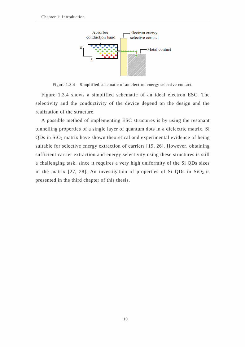
Figure 1.3.4 – Simplified schematic of an electron energy selective contact.
Figure 1.3.4 shows a simplified schematic of an ideal electron ESC. The
selectivity and the conductivity of the device depend on the design and the
realization of the structure.
A possible method of implementing ESC structures is by using the resonant
tunnelling properties of a single layer of quantum dots in a dielectric matrix. Si
QDs in SiO2 matrix have shown theoretical and experimental evidence of being
suitable for selective energy extraction of carriers [19, 26]. However, obtaining
sufficient carrier extraction and energy selectivity using these structures is still
a challenging task, since it requires a very high uniformity of the Si QDs sizes
in the matrix [27, 28]. An investigation of properties of Si QDs in SiO2 is
presented in the third chapter of this thesis.
10
Chapter 1: Introduction
11
1.4 Aim and structure of this thesis
The main aim of this thesis is to investigate and study different aspects of
hot carrier solar cells. This is a novel third generation device that, despite its
structural simplicity, presents a series of unique scientific and technological
challenges.
In particular in this thesis several of the main aspects related to the
development of a hot carrier solar cell are addressed.
The thesis is divided into six main chapters. At the beginning of each
chapter a comprehensive review of the most important papers on the specific
topic is presented, at the end of every chapter a summary of the key results is
reported.
In chapter two the calculation of the main efficiency limits for solar energy
conversion is presented and discussed in detail, together with preliminary
calculations of hot carrier solar cells efficiency limits. The main body of the
chapter is dedicated to the presentation of a novel hybrid model for efficiency
calculation. This model takes into account, at the same time, physical aspects
that have been treated separately in previous models. In addition, the
calculation has been performed for a specific semiconductor, InN, taking into
account all the specific electronic and optical properties, in order to obtain
efficiency limits close to real values.
In chapter three the possibility of realizing energy selective contacts using
silicon quantum dots in a silicon dioxide matrix is evaluated. The structural and
optical characterization of silicon rich oxide layers is presented at the
beginning of the chapter. The remaining part is dedicated to the analysis of the
properties of a single layer of silicon quantum dots in silicon dioxide. In
particular the possibility of controlling quantum confinement properties of this
structure is demonstrated and effects of different annealing conditions and
regimes are investigated.

Chapter 1: Introduction
12
Chapter four is dedicated to the investigation of hot carriers relaxation
velocities in III-V semiconductors. In particular a comparison of time resolved
photoluminescence data for GaAs and InP is presented, in order to investigate
the hot phonon effect and intervalley scattering phenomena. In the second part
of the chapter hot carrier transients are studied for wurtzite InN. This allows
comparison of experimental data with theoretical results obtained in chapter
two.
Chapter five is the last main chapter of the thesis and is dedicated to a
comprehensive discussion of results obtained in the other sections of the thesis.
The main aim of this chapter is to analyse and bring into a common picture the
different aspects of the hot carrier solar cell and present further challenges
related to the development of a prototype device. This discussion leads to an
outline of the current state of research on hot carrier solar cells and highlights
the different areas and directions where future research should be focused.
In chapter six the conclusion from this thesis are presented.
Chapter 1: Introduction
13
1.5 Bibliography
1. U.S. department of Energy, International energy outlook. Washinton
DC. 2010. p. 338.
2. Solarbuzz, Marketbuzz. www.solarbuzz.com. 2010.
3. Ginley, D., M.A. Green, and R. Collins, Solar energy conversion toward
1 terawatt. Mrs Bulletin, 2008. 33(4): p. 355-364.
4. Renewable Energy Policy Network for the 21st Century, Renewables
2010 global status report. 2010. p. 80.
5. Green, M.A., Crystalline and thin-film silicon solar cells: state of the
art and future potential. Solar Energy, 2003. 74(3): p. 181-192.
6. Chapin, D.M., C.S. Fuller, and G.L. Pearson, A new silicon p-n junction
photocell for converting solar radiation into electrical power. Journal of
Applied Physics, 1954. 25(5): p. 676-677.
7. Shi, Z., S. Wenham, and J. Ji. Mass production of the innovative pluto
solar cell technology. in 34th Ieee Photovoltaic Specialists Conference.
2009.
8. Zhao, J., A. Wang, and M.A. Green, High-efficiency PERL and PERT
silicon solar cells on FZ and MCZ substrates. Solar energy materials
and solar cells, 2001. 65(1-4): p. 429-435.
9. Green, M.A., Consolidation of thin-film photovoltaic technology: The
coming decade of opportunity. Progress in Photovoltaics, 2006. 14(5): p.
383-392.
10. Hirst, L.C. and N.J. Ekins-Daukes, Fundamental losses in solar cells.
Progress in Photovoltaics: Research and Applications, 2010.
11. Shockley, W. and H.J. Queisser, Detailed balance limit of efficiency of
p-n junction solar cells. Journal of Applied Physics, 1961. 32(3): p. 510-
519.
12. Landsberg, P.T. and G. Tonge, Thermodynamic energy conversion
efficiencies. Journal of Applied Physics, 1980. 51(7): p. R1-R20.
13. Conibeer, G., et al., Silicon nanostructures for third generation
photovoltaic solar cells. Thin Solid Films, 2006. 511: p. 654-662.

Chapter 1: Introduction
14
14. Cuadra, L., A. Marti, and A. Luque, Present status of intermediate band
solar cell research. Thin Solid Films, 2004. 451: p. 593-599.
15. Dimroth, F., High-efficiency solar cells from III-V compound
semiconductors. Physica Status Solidi C - Current Topics in Solid State
Physics, 2006. 3(3): p. 373-379.
16. Guter, W., et al., Current-matched triple-junction solar cell reaching
41.1% conversion efficiency under concentrated sunlight. Applied
Physics Letters, 2009. 94(22): p. 223504.
17. Green, M.A., Third generation photovoltaics: advanced solar
conversion. 2003: Springer-Verlav.
18. Ross, R.T. and A.J. Nozik, Efficiency of hot carrier solar energy
converters. Journal of Applied Physics, 1982. 53(5): p. 3813-3818.
19. Conibeer, G., C.W. Jiang, D. König, S.K. Shrestha, T. Walsh, and M.A.
Green, Selective energy contacts for hot carrier solar cells. Thin Solid
Films, 2008. 516(20): p. 6968-6973.
20. Conibeer, G., D. König, M.A. Green, and J.-F. Guillemoles, Slowing of
carrier cooling in hot carrier solar cells. Thin Solid Films, 2008.
516(20): p. 6948-6953.
21. Shrestha, S.K., P. Aliberti, and G. Conibeer, Energy selective contacts
for hot carrier solar cells. Solar energy materials and solar cells, 2010.
94(9): p. 1546-1550.
22. Othonos, A., Probing ultrafast carrier and phonon dynamics in
semiconductors. Journal of Applied Physics, 1998. 83(4): p. 1789-1830.
23. Pötz, W. and P. Kocevar, Electronic power transfer in pulsed laser
excitation of polar semiconductors. Physical Review B, 1983. 28(12): p.
7040-7047.
24. van Driel, H.M., X.Q. Zhou, W.W. Ruhle, J. Kuhl, and K. Ploog,
Photoluminescence from hot carriers in low temperature grown GaAs.
Applied Physics Letters, 1992. 60(18): p. 2246-2248.
25. Patterson, R., M. Kirkengen, B. Puthen Veettil, D. Konig, M.A. Green,
and G. Conibeer, Phonon lifetimes in model quantum dot superlattice
systems with applications to the hot carrier solar cell. Solar energy
materials and solar cells. 94(11): p. 1931-1935.

Chapter 1: Introduction
15
26. Jiang, C.W., M.A. Green, E.C. Cho, and G. Conibeer, Resonant
tunneling through defects in an insulator: Modeling and solar cell
applications. Journal of Applied Physics, 2004. 96(9): p. 5006-5012.
27. Aliberti, P., Y. Feng, Y. Takeda, S.K. Shrestha, M.A. Green, and G.J.
Conibeer, Investigation of theoretical efficiency limit of hot carrier
solar cells with bulk InN absorber. Journal of Applied Physics, 2010.
108(9): p. 094507-10.
28. Berghoff, B., S. Suckow, R. Rolver, B. Spangenberg, H. Kurz, A.
Dimyati, and J. Mayer, Resonant and phonon-assisted tunneling
transport through silicon quantum dots embedded in SiO2. Applied
Physics Letters, 2008. 93(13): p. 132111.

Chapter 2
MODELLING EFFICIENCY LIMITS
FOR HOT CARRIER SOLAR CELLS

Chapter 2: Modeling Efficiency Limits of Hot Carrier Solar Cells
16
2.1 Introduction
The calculation of limiting efficiencies for solar convertors has been a topic
of research interest since the high potential of solar cells, as a source of
renewable energy, was discovered in the late fifties. The first consistent
theoretical approach for an efficiency limit calculation was developed by
Shockley and Queisser and was published during 1961 [1]. Previous work on
maximum efficiency calculation was based on experimental results and simple
theoretical models, limiting the validity of results to very particular conditions
[2-4]. These limits have been successively defined by Shockley as “semi-
empirical”, since they were not supported by a solid theoretical framework.
The Shockley-Queisser limit is currently still used in the photovoltaic
industry as reference for first generation, wafer-based, solar cells and is
considered to be one of the most important contributions to the photovoltaic
field. The efficiency limit calculated by Shockley and Queisser is also known
as “detailed balance limit”, because it is based on the balance of absorbed and
emitted photons assuming a planar geometry and blackbody radiation.
Improvements to the Shockley-Queisser formulation can be obtained by
associating a chemical potential to photons emitted by electron-hole
recombination according to the theory developed by P. Würfel and also
described by Green [5, 6].
The aim of current research in photovoltaics, beyond improving the
efficiency of wafer-based solar cells, is to engineer devices that are not bound
to the single junction configuration and thus can aim for efficiencies higher
than the detailed balance limit. In principle the efficiency limit for solar cells is
the thermodynamic limit, which is represented by the Carnot efficiency.
The thermodynamic limit has been accurately calculated by Landsberg,
considering a temperature of 6000 K for the sun and 300 K for the solar cell
and taking into account losses due to re-emitted energy and increased entropy
in the absorber [7]. The efficiency limit calculated by Landsberg is 93.3% and
drops to 85.4%, considering entropy increase due to extraction of useful
electrical energy through contacts [8].

Chapter 2: Modeling Efficiency Limits of Hot Carrier Solar Cells
17
The large difference between the thermodynamic efficiency limit and the
detailed balance limit leaves a wide margin for research in third generation
photovoltaics to overcome the Shockley-Queisser limit. The hot carries solar
cell (HCSC) is one of the most promising third generation concepts which aim
to reach efficiency limits close to the thermodynamic limit. The calculation of
limiting efficiency for HCSC has been a topic of research since the concept
was first investigated by Ross and Nozik [9]. In their work Ross and Nozik
assumed that the number of carriers extracted from the device is equal to the
difference between the incoming and the re-emitted number of photons. This
approach, called particle conservation (PC model), leads to efficiencies of 65%
for non-concentrated solar radiation and 85% for full concentration, assuming
the sun to be a blackbody at 6000 K and no carrier thermalisation. Würfel
calculated these efficiency values using a different approach and considering
Auger recombination (AR) and impact ionization (II) as predominant
phenomena in determining carrier distributions (AR-II model) [10]. Very fast
AR-II rates tend to keep carriers always in equilibrium driving the quasi-Fermi
level difference towards zero. For this model calculated efficiencies were of
85% for a 0 eV bandgap semiconductor at full solar concentration and no
thermalisation with the lattice. During 2005 Würfel et al. re-visited the
approach used by Ross and Nozik proving that the PC model was valid only in
particular conditions and could lead to “non-physical” solutions in some cases,
confirming that the effects of AR and II are definitely not negligible [11]. Both
PC and II-AR models have been revisited by Takeda et al. and researchers at
the ARC Centre of Excellence for Photovoltaics and Renewable Energy
Engineering [12-15]. The first two reports from Takeda et al. improved the
theoretical frameworks developed by Ross and Nozik and Würfel, including in
the model thermalisation effects for hot carriers and using a parabolic bands
approximation to represent the E-k relations for the absorber. Results of these
calculations have shown lower efficiency limits compared to previous reports,
and proved that the value of maximum efficiency is strictly related to the
thermalisation time. Despite the improvements in the theoretical description,
Takeda et al. confirmed that either the PC model or the AR-II model are only
valid in particular conditions. To overcome this problem and calculate

Chapter 2: Modeling Efficiency Limits of Hot Carrier Solar Cells
18
efficiencies close to real values, a new theoretical framework that includes the
effect of particle and energy conservation plus AR-II mechanism has been
developed and is described in this chapter. Using this model a maximum
efficiency value of 43.6% has been calculated considering bulk InN as absorber
material and a 5760 K blackbody as incoming radiation source and using a
reasonable estimate for attainable thermalisation rate [12].

Chapter 2: Modeling Efficiency Limits of Hot Carrier Solar Cells
2.2 Literature Review
2.2.1 Landsberg thermodynamic limit
Landsberg et al. calculated the thermodynamic efficiency limit for sunlight
energy conversion using a rigorous mathematical formalism during 1980 [7].
The efficiency limit has been calculated by considering entropies associated
with the exchanged energy fluxes and applying the second law of
thermodynamics. There are no other applied restrictions to the model, which
improves the Carnot description, being still based on pure thermodynamic
principles.
Figure 2.2.1 - Schematic diagram of energy converter in Landsberg model [7].
Figure 2.2.1 shows the energy and entropy fluxes considered by Landsberg
for the model. and represent the energy and entropy fluxes respectively
coming from the external environment into the convertor, associated with the
sun radiation.
pE pS
sE and sS are instead the outgoing energy and entropy fluxes
from the device; they can be represented as one or more couples of fluxes
depending on the energy and entropy sinks they are directed to. Q is the rate of
heat transfer to the surroundings at a temperature T. The energy and entropy
rates of change into the convertor are respectively and . E S gS is the entropy
generation rate into the convertor due to internal processes and is assumed to
have its minimum value at zero.
gsp
sp
STSTQSTST
WEQEE (2.2.1)
19

Chapter 2: Modeling Efficiency Limits of Hot Carrier Solar Cells
Equations (2.2.1) balance energy and entropy fluxes. Defining effective
temperature fluxes an overall balanced equation can be written following from
(2.2.1).
gFs
sFp
pj
jFj STW
TTE
TTESTEpsjS
ET 11;,...),( (2.2.2)
Considering for example the steady-state condition with no sinks
( ) the balance equation 0ss SESE (2.2.2) yields to the Carnot
efficiency.
FppWg
Fpp T
TE
WSTTTEW 1;1 (2.2.3)
The equality holds for the ideal limiting case where . 0gS
In general if the emission into a sink is also taken into account equation
(2.2.2) yields to:
p
s
FsFpW E
ETT
TT 11 (2.2.4)
Considering the conversion of blackbody radiation of temperature TR by a
converter at ambient temperature T, which emits blackbody radiation itself we
have:
4
3344
31
341
43;
34;
34;
34;;
RRW
RFpFsRpspps
TT
TT
TTTTTSTSTETE
(2.2.5)
The right-end side of equation (2.2.5) represents the ratio of available
energy of blackbody radiation, defined as the maximum amount of work that
can be provided, to its internal energy. This corresponds to an efficiency of
93.3% and represents the ultimate conversion limit for solar energy.
It has been stated that the Landsberg efficiency limit is not even correct in
principle due to entropy generation during light absorption [16]. These theories
however are based on reciprocity between light absorption and emission.
20

Chapter 2: Modeling Efficiency Limits of Hot Carrier Solar Cells
2.2.2 Shockley-Queisser approach
In the detailed balance approach Shockley and Queisser described the photon
flux emitted from the solar cell, due to radiative recombination, using equation
(2.2.7) and assuming a flat geometry [6, 8]. This is an approximation of the
generalized Planck formula, equation (2.2.6). The approximation is valid in
non-degenerated conditions, since the Bose-Einstein distribution is
approximately equivalent to Boltzmann-Maxwell distribution. is the
difference between electro-chemical potentials of electrons and holes and TC is
the carrier temperature, which is assumed to be in common for electrons and
holes. TC = 300 K in the Shockley-Queisser derivation. 22 d
3 2 / 1CgE kTE
Fh c e
(2.2.6)
/ /22C CkT kT
3 2g
E EF e e d
h c (2.2.7)
FE represents the number of emitted particles (photons) per unit area per unit
time (neglecting stimulated emission). In conventional solar cells the splitting
of electro-chemical potentials for electrons and holes is equal to the electric
potential difference neglecting contact losses, thus = q V.
If = 0 V equation (2.2.7) represents the radiative recombination rate at
equilibrium, F0.
/22CkT
0 3 2gE
F e dh c
(2.2.8)
The current density through the cell is the difference of the incoming photon
flux and the radiative recombination, multiplied for the elementary charge. CqkTV
A eFFqJ /0
(2.2.9)
22 A d/3 2 1Sg
A kTEF
h c e (2.2.10)
FA represents the number of incoming photons per unit area per unit time,
which is approximated with the blackbody radiation spectrum. A is the solid
angle subtended by the sun and is equal to the concentration ratio divided by
the maximum possible concentration ratio. TS = 5760 K is the temperature of
the black-body [17]. Solving the system of equations (2.2.6) - (2.2.10) the J-V
characteristics of the device can be calculated. The value of maximum 21

Chapter 2: Modeling Efficiency Limits of Hot Carrier Solar Cells
achievable efficiency can be derived as a function of the semiconductor
bandgap EG.
Figure 2.2.2 – Efficiency for a blackbody solar cell at TC = 300 K, with sun at TS = 6000 K,
as a function of the absorber material electronic bandgap EG for different values of the
parameter f, curve (a) f = 1, curve (b) f = 10-3, curve (c) f = 10-6, curve (d) f = 10-9, curve (e)
f = 10-12. f is a function of the solid angle subtended by the sun [1].
The detailed balance approach can be improved associating a chemical
potential with the emitted photon flux due to electron-hole radiative
recombination as proposed by Würfel et al. in 1982 [6]. This approach has been
investigated by Green et al. in 2003 [5]. In this case the emitted photon flux
will be a function of and cannot be approximated with (2.2.8) any longer,
but by the complete expression as in (2.2.6). This implies that the emitted
photon flux is a function of the electric potential across the device and
complicates the model slightly. The results obtained using this approach are not
far from the ones calculated by Shockley and Queisser, but the method can be
applied in a wider range of cell operating conditions.
2.2.3 Ross and Nozik approach for calculation of hot carrier
solar cell efficiency
In their paper published in 1982 Ross and Nozik theorized the concept of
HCSC calculating limiting efficiency with an approach similar to the detailed
balance [9]. In this case the carrier system has a temperature, TC, much higher
than the external environment and the solar converter TRT. Carriers are
extracted through ESCs. 22
Chapter 2: Modeling Efficiency Limits of Hot Carrier Solar Cells
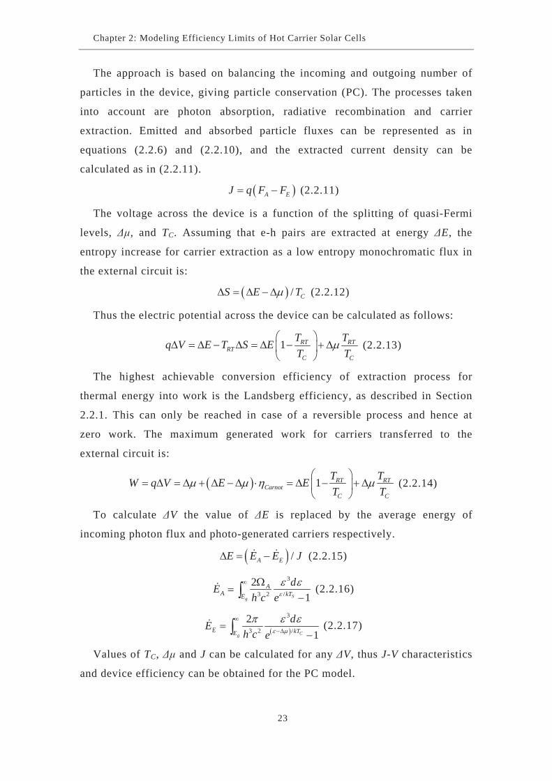
The approach is based on balancing the incoming and outgoing number of
particles in the device, giving particle conservation (PC). The processes taken
into account are photon absorption, radiative recombination and carrier
extraction. Emitted and absorbed particle fluxes can be represented as in
equations (2.2.6) and (2.2.10), and the extracted current density can be
calculated as in (2.2.11).
A EJ q F F (2.2.11)
The voltage across the device is a function of the splitting of quasi-Fermi
levels, , and TC. Assuming that e-h pairs are extracted at energy E, the
entropy increase for carrier extraction as a low entropy monochromatic flux in
the external circuit is:
/ CS E T (2.2.12)
Thus the electric potential across the device can be calculated as follows:
1 RT RTRT
C C
T Tq V E T S ET T
(2.2.13)
The highest achievable conversion efficiency of extraction process for
thermal energy into work is the Landsberg efficiency, as described in Section
2.2.1. This can only be reached in case of a reversible process and hence at
zero work. The maximum generated work for carriers transferred to the
external circuit is:
1 RT RTCarnot
C C
TW q V E ET T
T (2.2.14)
To calculate V the value of E is replaced by the average energy of
incoming photon flux and photo-generated carriers respectively.
/A EE E E J (2.2.15)
3
/3 2
21Sg
AA kTE
dEh c e
(2.2.16)
3
3 2 /
21Cg
E kTE
dEh c e
(2.2.17)
Values of TC, and J can be calculated for any V, thus J-V characteristics
and device efficiency can be obtained for the PC model.
23

Chapter 2: Modeling Efficiency Limits of Hot Carrier Solar Cells
3
/3 20
21S
AMPP MPP kT
dJ Vh c e
(2.2.18)
Figure 2.2.3 – Efficiency of an ideal hot carrier converter at 1 sun as a function of absorber
material electronic bandgap EG for different carrier temperatures TC [9].
In Figure 2.2.3 the curve at 300 K corresponds to the detailed balance limit.
Increasing the temperature of extracted carrier values of efficiency up to 65%,
for one sun, incoming radiation are predicted by the PC model for the HCSC.
2.2.4 Auger recombination-impact ionization model
The PC model is only valid in particular conditions. In fact AR and II have a
significant effect on the performances of the HCSC.
The high carrier temperatures imply high rates of AR/II possibly comparable
with the radiative recombination rate. When II and AR are taken into account
then particle number is no longer conserved. Würfel calculated the HCSC
efficiency limit using a model entirely based on AR/II, assuming infinitely
short lifetimes for these two processes [10]. AR and II are processes which
tend to maintain the equilibrium of electro-chemical potentials for electrons
and for holes. Having very high AR/II rates tends to reduce the splitting of
quasi-Fermi levels. For ultrafast AR/II the value of is considered to be
always zero. Therefore, the energy flux of extracted carriers can be expressed
as a function of carrier temperature.
24

Chapter 2: Modeling Efficiency Limits of Hot Carrier Solar Cells
3 3
/ /3 2 3 2
2 21 1S Cg g
Aextract A E kT kTE E
d dE E Eh c e h c e
(2.2.19)
The extracted current density is the extracted power divided by the
extraction energy level. 3 3
/3 2 3 2
2 21 1S Cg g
extract AkT kTE E
qE q dJE E h c e h c e /
d (2.2.20)
The voltage can be expressed as extracted carrier energy flux multiplying
Carnot efficiency.
1 RT
C
TqV ET
(2.2.21)
Given the properties of incoming radiation and the value of absorber
material bandgap, the output power from the solar convertor can be calculated
as a function of carrier temperature. Therefore, the efficiency of the device is
obtained as a function of absorber material bandgap, EG.
Figure 2.2.4 - Efficiency of a hot carrier converter as a function of absorber material
electronic bandgap EG for (a) maximum concentrated, (b) unconcentrated AM0 radiation [10].
For this model the efficiency has no dependence on the hot carrier extraction
energy level. A higher extraction level increases the extraction voltage and
reduces the current at the same time due to increasing AR rate which tends to
promote carriers to high energy levels. The energy is conserved for every AR/II
event, thus only thermal energy is involved in the model, leading to a constant
Carnot efficiency.
25

Chapter 2: Modeling Efficiency Limits of Hot Carrier Solar Cells
2.2.5 Introduction of thermalisation time and absorber E-k
relation
Both the Ross and Nozik (PC) and Würfel (AR/II) models take into account
the absorber of the HCSC only considering the electronic bandgap EG.
Absorber physical and electronic properties are not considered. This simplifies
the mathematical analysis making the models completely general but not
sufficiently accurate.
During 2008 and 2009 Takeda et al. investigated both PC and AR/II models,
improving both theoretical frameworks, including effects of carrier
thermalisation time constant, TH, and relations between carrier density, nC, and
quasi-Fermi potentials, , considering parabolic E-k dispersion relations [13,
14].
The analysis from Takeda et al. follows the approach used by Ross and
Nozik introducing equations to model the loss of energy due to thermalisation.
TH
RE
Sg
S
eF
kTEFF
dee
chEJ
RTg
kTE
kT
A
)3)(1(~11
23~2 32
(2.2.22)
Equations (2.2.22) represent the conservation of energy. The thermalisation
time, TH, is the average time that hot carriers spend in the absorber before
relaxing towards band edges. The retention time, RE, is the average time that
hot carriers spend in the absorber before being extracted into the ESCs. The
thermalisation time is assumed to be the same for electrons and holes at any
carrier temperature.
13/2
32
8 2 / 2 1e
Cg
C
kTeEC g
nd
mn E eh
A REF
d (2.2.23)
Equations (2.2.23) are two separate ways to calculate the carrier density.
Either by relating to the retention time or to the quasi-Fermi electron potential,
26

Chapter 2: Modeling Efficiency Limits of Hot Carrier Solar Cells
e. A parabolic approximation for both conduction and valence bands has been
assumed.
Results of this model show that the efficiency of the final device is a strong
function of the thermalisation time, Figure 2.2.5. This is confirmed also by
results presented in the next section of this chapter, where it has been
demonstrated that the carrier relaxation can be completely described with an
exponential energy decay process, which is a function of the thermalisation
velocity, as shown in equation (2.3.6), thus is not necessary to include the
retention time as a parameter in the model.
Figure 2.2.5 - Conversion efficiency and optimal bandgap versus carrier thermalisation time
for 1000 suns concentration [13].
It can be noted that for shorter thermalisation times the optimum bandgap
rises. This is because the shorter TH results in significant thermalisation and
hence need to stop carriers losing too much energy before extraction. This
offsets the advantage for current of having a narrower band gap.
27

Chapter 2: Modeling Efficiency Limits of Hot Carrier Solar Cells
28
2.3 Modelling efficiency limit for a hot carrier
solar cell with an indium nitride absorber
In this section results on the efficiency modelling of a HCSC with a bulk
InN absorber are presented. A hybrid model has been implemented, which
allows a quantitative combination of particle and energy balance and influence
of AR and II. The detailed band structure of bulk wurtzite InN has been
considered in the calculation of carrier densities. Real data for II-AR time
constants and realistic values of thermalisation rates have been used to
calculate carrier energies. The model includes both thermodynamic and kinetic
equations in order to calculate the realistic conversion efficiency limit for an
InN based HCSC.
The main reason for selecting InN as absorber material is the combination of
electronic and phononic properties. It has a small electronic band gap (0.7 eV)
for better light absorption, at the same time it has a very wide gap between
acoustic and optical branches in the phonon dispersion characteristic, allowing
slower thermalisation of hot carriers by suppression of optical to acoustic
phonon decay via the specific Klemens’ decay processes [18-20].
2.3.1 Model assumptions
The HCSC has been treated as a system which can interact with the external
environment through exchange of particles and energy fluxes. Hot electrons
and holes are extracted to the external circuit through ESCs, which in this
model have been considered to be ideal, such that they have infinite
conductivity and a very narrow allowed energy range for transmission.
Different realization techniques for ESCs are currently under investigation. A
promising approach, for instance, is using silicon quantum dots in a SiO2
matrix as a double barrier resonant tunneling structure [21-23]. For the
absorber hot Fermi distributions are assumed, for electrons and holes due to
fast carrier-carrier scattering rate. A common temperature value for hot
electrons and holes has also been assumed [24]. These assumptions have also

Chapter 2: Modeling Efficiency Limits of Hot Carrier Solar Cells
been considered in other reports [11, 20]. Other authors consider holes to be
always close to the lattice temperature, due to their high effective mass, with
only electrons being at a higher non-equilibrium temperatures [25].
2.3.2 Modelling of J-V characteristics
Figure 2.3.1 – (a) Simplified diagram of a HCSC with indication of major parameters used for
modelling. Eg (absorber electronic bandgap), μe (electrons chemical potential), μh (holes
chemical potential), μ (μe + μh + Eg), E (extraction energy of hot carriers). (b) Schematic
representation of energy and particle fluxes interactions used in the model (particle fluxes -
full arrows, energy fluxes - dotted arrows).
Figure 2.3.1 (a) shows a simplified diagram of a HCSC with important
parameters used for modelling. Figure 2.3.1 (b) shows the energy and particle
fluxes involved in the device operation. The particle flux coming from the sun
can be approximated with a blackbody radiation spectrum as shown in equation
(2.2.10). The particle flux due to radiative recombination is described as in
(2.2.6).
e h gE (2.3.1)
29
In equation (2.3.1) μe and μh represent quasi-Fermi energies of electrons and
holes measured from the conduction and valence band edges, respectively. μ

Chapter 2: Modeling Efficiency Limits of Hot Carrier Solar Cells
is the quasi-Fermi level separation, which includes the bandgap Eg, as shown in
(2.3.1).
Particle fluxes due to AR and II are calculated using coefficients derived for
bulk InN. Details of the derivation are reported in the next section.
, , , ,IA abs II e h C abs AR e h CF d R T d R T (2.3.2)
FIA is the particle flux associated with AR and II events. This is directly
related to total AR-II rates (RAR, RII) and to the absorber thickness dabs. The
current density in steady state can be calculated by balancing incoming and
outgoing particle and energy fluxes.
A E IAJ e F F F (2.3.3)
The calculation of current density as a function of carrier temperature and
quasi-Fermi levels, according to (2.3.3), is completely general and allows
computation of extracted current for a given extraction voltage across the
device.
AR and II rates depend on the quasi-Fermi level separation. A net AR rate is
obtained for positive μ and a net II rate for negative μ.
The flux of energy due to incoming solar illumination ( A) is considered
together with the energy flux emitted by the cell due to emission of photons
( E) and the flux due to carrier thermalisation process ( TH). 3
/3 2
21Sg
AA kTE
dEh c e
(2.3.4)
3
3 2 /
21Cg
E kTE
dEh c e
(2.3.5)
' , ' , ' , ' ,e e C e e RT h h C h h RTTH e abs h abs
TH TH
T T TE n d n d
T (2.3.6)
The energy flux due to electrons and holes thermalisation losses is shown in
equation (2.3.6). TRT is room temperature (300 K), TH is the characteristic
thermalisation lifetime for hot carriers, ne and nh are the electron and hole
densities respectively, 'e and 'h are the average energy values for electron and
hole populations. The net thermalisation loss is a function of the carrier
temperature and quasi-Fermi potentials.
30

Chapter 2: Modeling Efficiency Limits of Hot Carrier Solar Cells
The average energy decays during thermalisation towards ’e (μe, TRT) and
’h (μh, TRT), which are close to the thermal energy value 3kTRT. The energy
reference levels are the corresponding band edges.
0
0
,'
,
e e e Ce
e e e C
D f T d
D f T d (2.3.7)
0
0
,'
,
h h h Ch
h h h C
D f T d
D f T d (2.3.8)
In equations (2.3.7) and (2.3.8) De( ) and Dh( ) represent the electron and
hole densities of states whilst fe and fh are the electron and hole occupancy
probabilities. The sub-picosecond carrier to carrier scattering rate justifies the
assumption of hot populations distributed according to Fermi-Dirac statistics
and hence fe and fh will depend exponentially on TC, Ee and Eh respectively.
Thus TH represents an exponential decay of hot carrier energy. However, the
consideration of non-equilibrium AR and II coefficients can modify
occupancies as discussed below. The product of the extracted current and the
extraction energy represents the “extracted energy flux” and can be calculated
balancing the three energy fluxes as in equation (2.3.9).
THEA EEEqEJ (2.3.9)
Here J is the extracted current as in (2.3.3) whilst E represents the
extraction energy of hot carriers from the absorber as shown in Figure 2.3.1.
This value is fixed and depends on the properties of the ESCs [22]. Even
assuming ideal ESCs, and hence isoentropic carrier transfer, the voltage of
carriers in the external circuit, V, must be lower than E/e. This is described
by a Carnot type relation between the voltage across the device and the
extraction energy [9].
1 1 RT RT
C C
T TV Ee T T
(2.3.10)
31

Chapter 2: Modeling Efficiency Limits of Hot Carrier Solar Cells
32
2.3.3 Carrier density calculation
To be able to calculate the J-V characteristic of the HCSC using the
equations described above, a relation between carrier density, electron and hole
quasi-Fermi levels and carrier temperatures for bulk wurtzite InN is necessary.
The carrier density can be calculated from the electron and hole densities of
states, which can be obtained from the dispersion relation.
E-k relations for high purity wurtzite InN have been calculated by Fritch et
al. using an empirical pseudopotential method [19]. Results of the calculations
illustrate that, in the energy range of interest for solar cells, wurtzite InN shows
two separated bands at the point plus a satellite band at the M-L symmetry
point, along the crystal direction for the conduction band. For the valence
band the calculation confirms two main bands with a point of degeneration at
, which can be identified as heavy and light hole bands, in addition a
separated split-off band is considered.
A multivalley approximation for the bulk InN band structure which takes
into account the three lowest conduction band minima ( 1, 3 and M-L) and
three hole valleys for the valence band has been used for calculations. The non-
parabolicity of InN main conduction band has also been considered. Parameters
for effective masses in satellite bands and non-parabolicity coefficients are
reported in Table 2.3.1 [19, 26].
Conduction Band Valence Band
1 3 M-L 1 (HH) 2 (LH) 3 (SO)
Effective mass m/m0 0.04 0.25 1 2.827 0.235 0.479
Non-parabolicity factor 1.43 0 0 0 0 0
Intervalley Energy Separation (eV) 0 1.77 2.71 0 0 0.25
Number of equivalent valleys 1 1 6 1 1 1
Table 2.3.1 - Model parameters for bulk indium nitride conduction and valence bands. Values
have been extracted from Fritch et al. [19].

Chapter 2: Modeling Efficiency Limits of Hot Carrier Solar Cells
2.3.4 Auger recombination and impact ionization coefficients
calculation
The influence of AR-II on the efficiency of the HCSC has been taken into
account amending the expression for the total current from the cell, as shown in
equation (2.3.3). Such a modelling approach allows consideration of II-AR
effects for all operating regimes of the HCSC. AR-II rates have been calculated
considering the three most probable processes for bulk InN, CCCH, CHHS,
CHHL, as reported by Dutta et al. [27], and neglecting high k-vector
mechanisms [28-30]. The phonon-assisted and trap-assisted AR-II processes
have been neglected because of the InN narrow electronic bandgap. The band
structure used for the II-AR rate computation is the same as for carrier density
calculations. The momentum conservation arises from the assumption of the
states as being the product of a plane wave and a Bloch function [27]. The
CCCH AR process involves three conduction band electrons and one hole. A
conduction band electron recombines with a hole, giving energy to a second
conduction band electron and raising it to a higher energy level. CCCH was
first investigated by Beattie et al [31]. 4
03 2
32 c CHCCCH
g
e mR Ih E
(2.3.11)
A simplification of the rate expression was formulated by Dutta et al. [27]
and is used in equation (2.3.11) with a technique developed by Sugimura [32].
The integral I can be evaluated according to (2.3.12). Definitions for functions
F and G can be found in [27], Z1 and Z2 are calculated as in (2.3.13).
1
2 21 2 1 2 1 2 1 2 00
, , 1 cA ZI dZ dZ F Z Z G Z Z Z Z J f 2' (2.3.12)
021 1 2 2' ; ' ;
1 2c
v
Z k Z km
' mk (2.3.13)
The CHHS AR process involves one electron, two heavy holes and a split-
off band hole. A conduction band electron recombines with a hole in the HH
band giving energy to another hole which can then move from the HH band to
the SH band. The rate for this process has also been investigated by Beattie et
33
Chapter 2: Modeling Efficiency Limits of Hot Carrier Solar Cells
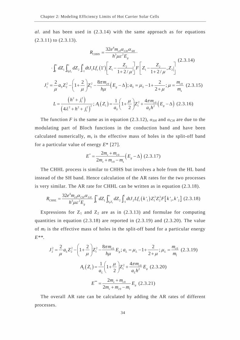
al. and has been used in (2.3.14) with the same approach as for equations
(2.3.11) to (2.3.13).
1 1
40
3 2
12 2
1 2 1 1 10 1
32
1' ,1 2 / 1 2 /
c CH SHCHHS
g
cA Z
e mRh E
Z ZdZ dZ dtJ Lf Z F Z Z2
(2.3.14)
2 2 2 0 01 2 1
82 2 21 ; 12
c cS g S S ;
s
m mJ a Z Z E ah m
(2.3.15)
2 21 2 0
1 1 12 22 2 21
41; 124
cg
S S
h j mL A Z Za a hh j
E (2.3.16)
The function F is the same as in equation (2.3.12), SH and CH are due to the
modulating part of Bloch functions in the conduction band and have been
calculated numerically, ms is the effective mass of holes in the split-off band
for a particular value of energy E* [27].
* 0
0
22
v cg
v c s
m mE Em m m
(2.3.17)
The CHHL process is similar to CHHS but involves a hole from the HL band
instead of the SH band. Hence calculation of the AR rates for the two processes
is very similar. The AR rate for CHHL can be written as in equation (2.3.18).
2 1
4 1 2 201 2 2 1 1 2 13 2 0 1
32 ' 'c CH LHCHHL cA Z
g
e m2, 'R dZ dZ dtJ Lf k Z Z F k k
h E (2.3.18)
Expressions for Z1 and Z2 are as in (2.3.13) and formulae for computing
quantities in equation (2.3.18) are reported in (2.3.19) and (2.3.20). The value
of ml is the effective mass of holes in the split-off band for a particular energy
E**.
2 2 2 0 02 2 1
82 2 21 ; 1 ;2
c cL g L L
l
m mJ a Z Z E ah mL (2.3.19)
2 02 1 1 2
41 12
cg
L L
mA Z Za a
Eh
(2.3.20)
** 0
0
22
v cg
v c l
m mE Em m m
(2.3.21)
The overall AR rate can be calculated by adding the AR rates of different
processes. 34

Chapter 2: Modeling Efficiency Limits of Hot Carrier Solar Cells
AR CCCH CHHS CHHLR R R R (2.3.22)
II can be considered as the inverse process of AR. Highly energetic carriers
impact with carriers bound in the lattice, ionizing them and creating new
electron-hole pairs. The total II rate is the summation of II rates for different
mechanisms and is calculated from the total AR rate [27].
Bk TII ARR R e (2.3.23)
Thus for = 0 the II and AR rates are the same and cancel out, such that
particle number is conserved and both electron and hole populations can be
described by the same Fermi-temperature. If is positive the II rate is less
than that for AR. This is the case when carrier extraction is not immediate and
there is a build-up of generated carriers such as to create a positive chemical
potential, . There is therefore pressure to reduce the particle number and AR
processes dominate. On the other hand, if is negative then the II rate is
greater than that for AR, implying a faster carrier extraction compared to
generation. This will in turn suppress emission and drive the particle number to
increase through II.
2.3.5 Hot carrier solar cell efficiency calculation
As every flux mentioned in the previous sections is a function of and TC,
these two parameters can be calculated, together with current density J, solving
numerically equations (2.3.3), (2.3.9) and (2.3.10). The solar cell efficiencies
have been calculated as the ratio of extracted power at the MPP of operation
and the total power in the incoming spectrum, Pin. Pin is the sum of all the
photon energies, multiplied by their individual intensities, IA.
in
J VP
(2.3.24)
0in AP I d (2.3.25)
35

Chapter 2: Modeling Efficiency Limits of Hot Carrier Solar Cells
36
2.3.6 Variation of conversion efficiency with carriers
extraction energy
The system of equations reported in the previous sections can be solved
using numerical methods and assuming particular constraints for the operation
of the solar cell. The current density J can be calculated for a given voltage V
across the device terminals, fixing the absorber thickness and thermalisation
velocities. Results presented in this section have been calculated for no
concentration ( A = 6.8 × 10⁻⁵), the maximum concentration ratio ( A = 1) and
a concentration ratio of 1000 suns ( A = 0.068), the last of which appears to be
the upper limit for practical achievable concentration in solar cells [33]. An
absorber thickness dabs = 50 nm has been used, unless otherwise noted. A
thermalisation constant th = 100 ps has been adopted, as a reasonable
compromise between values recently reported in the literature [34-37]. In fact
the thermalisation velocity of hot carriers in InN is still under debate and
depends strongly on the quality of the films and deposition technique [34, 35].
Including the value of th in the kinetic equation (2.3.6) will certainly lead to an
efficiency limit lower than the thermodynamic limit discussed in previous
sections. The gap between the realistic efficiency limit and the thermodynamic
limit could be reduced if the carrier cooling velocity could be further reduced.
Figure 2.3.2 shows the dependence of the calculated efficiency on the
extraction energy E. For 1000 suns the efficiency curve reaches a peak value
of 0.436 for hot carrier extraction energy of 1.44 eV. Maximum efficiencies of
0.52 and 0.225 have been calculated respectively for full concentration and
non-concentrated spectra. For the maximum concentration case the dependence
on extraction energy is very flat. This is because, at these very high
illumination levels, thermalisation only plays a minor role compared to energy
flux associated with carrier generation. For the 1 sun and 1000 suns cases,
there is a broad optimum in extraction energy (at 1.47 eV and 1.45 eV
respectively) between not having it too low in order to maintain voltage, whilst
not having it too high such as to reduce current. This current limiting effect is
most marked when the extraction energy is higher than 1.62 eV, which is close
to the average energy of the incoming photon population. At the MPP, in order

Chapter 2: Modeling Efficiency Limits of Hot Carrier Solar Cells
to provide carriers to fill the gap denuded at the extraction energy, carriers are
forced to undergo AR. For these extraction energies the AR rate is larger than
the II rate, with a positive quasi-Fermi gap and a very low carrier temperature.
Figure 2.3.2 - HCSC efficiency as a function of carrier extraction energy level.
Thermalisation time is 100 ps, lattice temperature is 300 K. Absorber thickness is 50 nm.
2.3.7 Hot carrier solar cell operation analysis
In this section relations between main HCSC parameters and extraction
voltage are discussed, all the results presented here and in following sections
have been calculated considering a concentration ratio of 1000 suns, if not
otherwise stated. Figure 2.3.3 (a) shows J-V characteristics for the HCSC for
four different extraction energies. The value of VOC increases when the
extraction energy is increased according to equation (2.3.10). Under open
circuit conditions, as the carrier temperature TC is very high (1000 K), the VOC
is directly related to E. The short circuit current decreases monotonically as a
function of extraction energy due to the increase of AR events, which are
necessary to raise the carrier energies to the extraction level and hence drive
down μ.
37

Chapter 2: Modeling Efficiency Limits of Hot Carrier Solar Cells
38
Figure 2.3.3 - (a) J-V relations, (b) carriers temperature, (c) carriers densities, (d) quasi-
Fermi potentials separation, versus extraction voltage for different extraction energies.
The low voltage part of the relationships, Figure 2.3.3 (a) (dashed lines), has
been calculated considering unlimited II and AR rates. In fact, according to the
model, carrier temperatures at very low extraction voltages tend to be
extremely high, as shown in Figure 2.3.3 (b). Such high temperatures, and
hence high occupancy of high energy states, can enlarge II rates in order to
decrease carrier energies to the extraction level. In this regime the theoretical II
and AR rates, calculated as explained in the previous sections, are not exact,
since other multiple carrier generation mechanisms can be involved, preventing
further increase of carrier temperature. This allows TC to remain in a physically
acceptable range, and thus addresses the objection to the PC model discussed
by Würfel [11].
The value of 3000 K for carrier temperature has been used as the threshold
between current values calculated with the hybrid model presented here (TC <
3000 K) and values computed using the unlimited II/AR rates (TC > 3000 K)
[36]. This particular temperature value allows matching the two currents,

Chapter 2: Modeling Efficiency Limits of Hot Carrier Solar Cells
39
calculated with the two models, since the high II rate drives μ to very low
values, reducing carrier density and making thermalisation losses negligible.
Thus, the hybrid model at low voltages becomes similar to the II-AR model
[10, 38].
For an extraction energy of 1.6 eV the J-V curve of Figure 2.3.3 (a) shows
two possible stable steady states of operation at voltages close to the maximum
power point (MPP), which correspond to two possible solutions of the model.
For this particular value of E (bi-stable region) the device can work both in
AR regime and II regime, due to the interaction of AR and II processes with
carrier thermalisation. For the first solution (dotted line) the quasi-Fermi level
separation is positive, hence the AR rate is higher than the II rate, increasing
the average energy of the carrier distribution as shown in Figure 2.3.3 (d).
Although a fast thermalisation rate will offset this average energy increase. For
the second solution (continuous line) the quasi-Fermi level separation is
negative, hence the net II rate decreases the average carrier energy. This
decrease in energy appears similar to the carrier thermalisation process, but in
reality competes with it, as II also involves an increase in carrier number,
unlike thermalisation.
Figure 2.3.3 (b) shows that for higher extraction energy, the temperature of
carriers is low, 500 K for E = 1.8 eV at MPP. In this case the extraction
energy is higher than the average energy of absorbed photons and hence J
should be decreased, due to very significant AR (equation (2.3.3)), so that the
energy conservation represented by equation (2.3.9) stands. Although a net AR
rate is always present to increase the energy of carriers once, the role of even a
moderate thermalisation rate is enhanced in this regime and the carrier
temperature is reduced at all extraction voltages. II becomes negligible and
efficiency is basically related to the limitation of the AR rate, which depends
on the material dispersion relation. On the other hand for E < 1.62 eV the
MPP is in II regime. Here the carrier temperatures increase with extraction
energy and high values of temperature are observed at low extraction voltage
due to high II rate. Instead temperature drops with increasing voltage, reaching
acceptable values around MPP.

Chapter 2: Modeling Efficiency Limits of Hot Carrier Solar Cells
40
The quasi-Fermi level gap μ changes from large negative values, at low
voltages, to very small positive values, at open circuit conditions as shown in
Figure 2.3.3 (d). At low voltages radiative recombination is suppressed and
most of the photogenerated carriers are extracted from the device as current.
For such extraction voltages multiple electron-hole pair generation due to II is
dominant and AR is negligible. The high extraction current also keeps the
carrier density in the absorber low (1011 - 1012 cm-3), although extra carriers are
generated by II. With increasing voltage towards the VMPP, μ increases
towards small negative values, as shown in Figure 2.3.3 (c), contributing to the
increase in thermalisation losses. Higher carrier densities are reported when
voltage is increased because of the decrease in extraction current and despite
the increase in the emission due to the lower II rate, which also makes
thermalisation significant. At MPP carrier density values of 1016 cm-3 are
shown in Figure 2.3.3 (c) with carriers temperature below 1000 K for all
extraction energies considered, these being feasible values for an InN absorber
[35]. A very high carrier temperature has been found at low voltages for
extraction energies E < 1.62 eV, Figure 2.3.3 (b), with values reaching above
3000 K when approaching short circuit. In these conditions additional II
mechanisms will occur limiting the carrier temperature and the quasi-Fermi
level gap from reaching extremely high values, which are unphysical, as
explained in the previous section. This process acts as a self limiting
mechanism for carrier temperature, which is intrinsic in the nature of the
device and highlights the influence of II for cell operation [19]. After reaching
a minimum around the MPP, due to increased emission and thermalisation, the
carrier temperature increases again with voltage due to rapid increase of AR.
The fast increase of carrier temperature at low voltages is not observed at
higher extraction energies. For E = 1.8 eV the carrier temperature carries on
decreasing monotonically as the voltage approaches short circuit, reaching
values lower than the lattice temperature, TC < TRT. This condition, which
appears unphysical, is due to the fact that the extraction energy is too high
compared to the average energy distribution of incoming photons. As
previously discussed a very high AR rate is necessary to increase the average
carrier energy for extraction, suppressing temperature below TRT.

Chapter 2: Modeling Efficiency Limits of Hot Carrier Solar Cells
The absorber carrier density, Figure 2.3.3 (c), has a very strong influence on
cell performances, being strictly related to thermalisation losses, equation
(2.3.6). At open circuit, which is the starting operating condition of the solar
cell, a relatively high carrier density is calculated (nC 1017 cm-3) due to low
extraction. In this case the value of nC is mainly related to the incoming
particles flux, radiative emission and AR. On decreasing the extraction voltage,
the carrier density deceases to about 1016 cm-3 at VMPP. A further decrease of
the voltage causes an additional reduction of nC related to the temporary large
increase of carrier extraction rate. The carrier density drop is only partially
compensated by the increase of II rate, but this is only a second order effect.
On the other hand only a very moderate decrease of nC is observed for
extraction energy of 1.8 eV, which indicates a relatively faster stabilization of
nC in response to voltage variation.
2.3.8 Calculation of Auger recombination and impact
ionization rates
Total rates for AR and II as function of voltage have been calculated using
equation (2.3.23) and results are plotted in Figure 2.3.4 (a,b). AR and II
lifetimes are calculated dividing the carrier density by the rate [14].
;CAR II
AR II
n CnR R
(2.3.26)
Under open circuit conditions the lifetime for AR is shorter than the lifetime
for II. AR lifetime is slightly higher than the carrier thermalisation constant
(100 ps). This implies that the average energy increase due to AR is negligible
compared to thermalisation losses, hence the average kinetic energy of new
photogenerated carriers is dissipated by thermalisation. On decreasing the
voltage towards VMPP an increase in AR and II lifetimes is observed, together
with decreasing of thermalisation losses, Figure 2.3.5 (a). For further decrease
of the voltage AR and II rates show opposite trends due to the inversion of the
quasi-Fermi energy gap. In terms of device operation this means that AR is
negligible at low voltages and II plays the dominant role in determining the
carrier distribution properties ( E < 1.62 eV) and allows the temperature to be 41

Chapter 2: Modeling Efficiency Limits of Hot Carrier Solar Cells
contained whilst increasing the number of carriers available for extraction. For
extraction energy of 1.8 eV no inversion of μ is observed and the carrier
temperature drops monotonically towards the lattice temperature in the low
voltage regime.
Figure 2.3.4 - AR and II lifetimes versus extraction voltage for different extraction energies.
2.3.9 Thermalisation losses and efficiency versus
thermalisation time
Most of the conclusions reached by analysing AR and II rates match quite
well with results shown in Figure 2.3.5 (a), where the energy losses due to hot
carrier thermalisation are reported in units of eV per unit area per unit time.
42

Chapter 2: Modeling Efficiency Limits of Hot Carrier Solar Cells
Figure 2.3.5 - (a) Thermalisation losses versus extraction voltage for different extraction
energies. Thermalisation constant is 100 ps. (b) Calculated efficiency limit versus
thermalisation constant.
The quasi-exponential increase of thermalisation losses with extraction
voltage, given a constant TH, is mainly due to the increase in carrier density.
These results confirm that, even considering AR and II in the calculation, the
value of TH has still a major influence on the final device efficiency. Figure
2.3.5 (b) shows calculated efficiency as a function of the TH for different
extraction energies. For very fast thermalisation ( TH = 10-14 s) an efficiency of
22.3% is calculated. This value does not depend on E and is very close to the
Shockley-Queisser efficiency limit for bulk InN when AR is taken into account.
Increasing the value of TH, a splitting of the efficiency curves for different E
has been found. This is due to the complex interaction between carrier
43

Chapter 2: Modeling Efficiency Limits of Hot Carrier Solar Cells
thermalisation and the influence of AR and II. A monotonic fast increase of
efficiency is shown for all extraction energies when TH is between 0.1 ps and 1
μs. For TH = 10-10 s, which is the value used for all the calculations presented
in the previous sections, four different values of efficiency can be identified
along the black vertical line in Figure 2.3.5 (b). In this particular case TH is
closer to the AR and II lifetimes at the MPP. These are respectively AR = 4.5 ×
10-9 s and II = 3.21 × 10⁻⁷ s for E = 1.6 eV and V = 0.72 V. This implies that
AR/II processes begin to have enough time to supply carriers for extraction
before complete thermalisation. A further increase of TH leads to a significant
increase of efficiency until it reaches saturation at TH = 1 ms, = 73%. In this
region does not depend on E, indicating that the II-AR model can be applied
with a high accuracy. This result determines for the first time the region of
validity of the II-AR model, which was demonstrated to be valid only in
particular conditions by Takeda et al [14]. In general this region is
characterized by AR,II << TH, which implies that the carrier energy distribution
can be affected by AR and II before thermalisation, hence the extraction energy
does not play a major role when thermalisation processes are reasonably slow.
2.3.10 Efficiency computation with indium nitride
absorption coefficient
The results of the calculations shown in the previous sections of this report
assume ideal absorption properties, which imply that every incoming photon
with energy above the bandgap is absorbed and generates an electron-hole pair.
In this section, results of efficiency computation and J-V characteristics are
reported based on the actual bulk InN absorption coefficient. Real absorption
properties have also been used to modify the ingoing and outgoing particle
fluxes, FA and FE, according to the generalized Kirchhoff law for thermal
photon currents emitted by a non-black emitter [6]. 2
/3 2
2'1Sg
AA kTE
dF ah c e
(2.3.27) 2
3 2 /
2'1Cg
E kTE
dF ah c e
(2.3.28)
In equations (2.3.27) and (2.3.28) ( ) represents absorptivity as a function
of the energy for bulk wurtzite InN. Data for InN absorption coefficient can 44

Chapter 2: Modeling Efficiency Limits of Hot Carrier Solar Cells
be found in the literature and are plotted in Figure 2.3.6 together with the PL
signal and the approximation used in the calculation [39]. The value of
absorptivity can be calculated from the absorption coefficient according to
equation (2.3.29), where dabs is the InN layer thickness.
1 absda e (2.3.29)
In Figure 2.3.7 (a,b) the efficiencies of the HCSC for different thicknesses
of the absorber layer are shown. For all the extraction energies the efficiency
increases in the first region of the plot, dabs < 1000 nm, and decreases for a
thicker absorber. These opposing trends are due to the influence on efficiency
of the competitive interaction between thermalisation and absorption. On
increasing dabs a larger quantity of light is absorbed, thus more photo-generated
carriers are available for extraction, which results in an efficiency increase. At
the same time there is a net increase of losses due to hot carrier thermalisation,
as evidenced in equation (2.3.6). In reality, on increasing dabs there is also a net
decrease in carrier density, which would lead to smaller thermalisation losses,
but this is a second order effect. Instead, when thermalisation losses begin to
play a major role, the efficiency starts to drop. Such behaviour is more or less
pronounced depending on E. Figure 2.3.7 (b) shows that at higher extraction
energies the efficiency peak occurs at lower absorber thickness and in addition
the slope of the curve is more pronounced. This confirms that high
thermalisation losses cause a drop in the average carriers energy making
extraction more difficult and so requiring a higher AR rate for larger extraction
levels.
Figure 2.3.6 - Bulk InN absorption coefficient from [39] (dashed line) and approximation
used for calculation (solid line), (inset) InN photoluminescence signal.
45

Chapter 2: Modeling Efficiency Limits of Hot Carrier Solar Cells
The value of maximum efficiency is considerably lower when real
absorption properties are taken into account, Figure 2.3.7 (c), compared to the
case of ideal absorption, 0.436 and 0.322 respectively. This implies that to gain
both the increased absorption and reduced thermalisation a light trapping
technique has to be implemented on a thin absorber. Using an effective light
trapping scheme the effective light path in the absorber can be enlarged,
increasing absorption without changing physical thickness and allowing
thermalisation losses to remain moderate. Different techniques to implement
light multiple passes are currently implemented in conventional and thin film
solar cells and could potentially be transferred to HCSCs [40].
46
Figure 2.3.7 - (a) Efficiency limit versus extraction energy for different absorber thicknesses.
(b) Efficiency limits versus absorber thickness for different extraction energies. (c) J-V
relations for different absorber thicknesses. Thermalisation constant is 100 ps.

Chapter 2: Modeling Efficiency Limits of Hot Carrier Solar Cells
2.4 Efficiency limit calculation with non ideal
energy selective contacts
Results presented in Section 2.3 of this chapter are calculated assuming ideal
ESCs for the HCSC as explained in Section 2.3.1. This implies that the
extraction energy level for ESCs is discrete and there are no resistive losses in
the ESCs, thus there is no entropy increase during carrier extraction. In reality
there is an entropy increase during the carrier extraction process which limits
its efficiency to values lower than Carnot efficiency.
In this section results of efficiency limits calculated taking into account non-
ideal energy selective contacts will be presented. In particular ESCs with a
finite energy transmission window ( E) have been considered, taking into
account contact resistance and entropy generation effects. Figure 2.4.1 shows
carriers transmission probability for ideal and non-ideal ESCs as a function of
energy.
Figure 2.4.1 - Carriers transmission probability versus energy for (a) ideal ESC, (b) non-ideal
ESC.
2.4.1 Theoretical description of non-ideal energy selective
contacts
The flux of current travelling through the ESCs towards the cold metal
electrodes can be described using the following relation.
, ,, , , , 3min 0 0
( ) ( )z
C e h rt e h
y ze h e h T T V y z
y z
dk dkeJ T f f d dd d
(2.4.1)
47

Chapter 2: Modeling Efficiency Limits of Hot Carrier Solar Cells
The current density in this case is proportional to the occupation probability
at the two sides of the ESC. Figure 2.4.2 shows the simplified InN E-k
dispersion relation used for current calculation.
Figure 2.4.2 – Simplified diagram of InN E-k dispersion relation used for current density
calculation [41].
Equation (2.4.1) has been derived assuming no correlation of energy of
electrons in three different directions as shown in (2.4.2). This assumption is
acceptable if there is a parabolic dispersion relation at the minimum energy
point along the three different directions. In addition for this calculation ESCs
with a finite transmission energy window and a transmission probability equal
to 1, as in Figure 2.4.1 (x = 1) are considered.
zkykxkkzyx zyxzyx ; (2.4.2)
Based on the energy and carrier conservation, and TC at steady state are
calculated using equations similar to (2.3.3) and (2.3.9) as shown in (2.4.3).
0;0e
EEEEeJFFF J
THEAIAEA (2.4.3)
Parameters in (2.4.3) are the same as reported in Section 2.3.2.
2.4.2 Results of calculation of efficiency limit with non-ideal
energy selective contacts
In this section we report on results of calculation of limiting efficiency of
HCSC with an InN absorber using non-ideal ESCs modelled as described in the
previous section. Illumination conditions and physical parameters of the
absorber are same as in Section 2.3, apart from the fact that the ESCs
transmission energy window is not discrete but has a width E.
48

Chapter 2: Modeling Efficiency Limits of Hot Carrier Solar Cells
Figure 2.4.3 – (a) HCSC efficiency as a function of extraction width of ESCs for different
extraction energies E. (b) HCSC efficiency as a function of extraction energy E for
different ESCs energy width. Thermalisation time is 100 ps, lattice temperature is 300 K.
Absorber layer thickness is 50 nm.
The maximum efficiency has been found for a E between 1.15 eV and 1.2
eV with a transmission energy window E of 0.02 eV. The value of limiting
efficiency was 39.6% compared to 43.6% calculated in the previous section
using ideal ESCs. The drop of efficiency is mostly due to the decrease of open
circuit voltage related to the lower extraction level, equation (2.3.10). This is
partially compensated by an increase in extracted current due to increased II
rate.
49
Figure 2.4.3 (a) shows calculated efficiency as a function of E for several
values of extraction energy. In all the curves two different trends can be
identified. If the value of E is too close to zero, the efficiency is very low due
to low carriers extraction, thus a very small value of short circuit current. The
conductivity of the contact in this case is indefinitely large. Enlarging E the

Chapter 2: Modeling Efficiency Limits of Hot Carrier Solar Cells
50
number or carriers available for extraction increases, improving JSC and so the
efficiency. In general the efficiency peak has been found for values of E from
0.02 eV to 0.1 eV depending on the extraction energy E. For the
configurations which show higher efficiencies, E < 1.35 eV, the optimum
value of E goes from 0.02 eV to 0.05 eV. This result shows that the
transmission energy range has to be very small and confirms once again the
high selectivity requirements of ESCs for HCSC [22]. Recently Le Bris et al.
calculated efficiencies beyond the Shockley-Queisser limit using high pass
ESCs instead of band pass ESCs, but they used a simplified model considering
only PC conditions at full concentration [42]. In Figure 2.4.3 (b) the value of
maximum efficiency as a function of E is reported for different values of E.
It can be observed that for small transmission energy window the extraction
energy which allows maximum efficiency is lower compared to the one
calculated using ideal ESCs. This effect is related to the higher occupancy at
lower energies, which increases the value of JSC for contacts with a small
transmission window.
It has to be mentioned that a simpler configuration could be potentially used
for ESCs. This consists of a potential barrier at the contact with a height that
coincides with the peak of Boltzman distribution of the carriers at a specific
temperature. However, it has been found that such configuration introduces
additional losses limiting the excitation of low energy carrier to higher states,
thus further reducing the efficiency. This is also partially supported by results
in Figure 2.4.3, which shows a marked decrease in efficiency when the
transmission energy width of the contacts exceeds a certain threshold.

Chapter 2: Modeling Efficiency Limits of Hot Carrier Solar Cells
51
2.5 Summary
The calculation of efficiency limits for solar converters has been the topic of
research since the very first discovery of photovoltaic effect. Different
theoretical models have been proposed to calculate thermodynamics maximum
conversion efficiency limits of semiconductor based solar converters. The most
important theoretical works are reviewed in the first section of this chapter,
where the famous Shockley-Queisser limit is also derived. The gap between the
detailed-balance approach and the thermodynamic conversion limits justifies
recent research efforts in calculation of efficiency limits for third generation
devices.
The calculation of limiting efficiency of HCSC has been attempted since the
concept was first developed by Ross and Nozik. Several models have been
proposed over the last few years. Many of them improved significantly the
original theoretical framework, although including many assumptions and not
taking into account very important physical phenomena for semiconductors
such as AR and II. Also no significant effort was invested in specifying
properties of the material to achieve efficiency limits close to a real device.
To improve HCSC theoretical characterization, in this chapter, achievable
efficiencies for HCSC have been calculated using bulk wurtzite InN as
absorber layer. A hybrid model, which takes into account both particle balance
and energy balance, has been implemented and adopted for calculations. The
model also considers influence of real AR and II rates on cell performances for
the first time. In addition actual thermalisation losses are included. AR-II rates
have been calculated including the most important three-carrier interaction
mechanisms which can occur in InN, at energies of interest for solar
applications.
The real InN dispersion relation has been reconstructed using actual
effective masses for different bands and non-parabolicity coefficients. The
limiting efficiency as a function of carrier extraction energy has been studied
for a fixed absorber thickness and thermalisation constant. A maximum
efficiency of 0.436 has been found for 1000 suns solar concentration and

Chapter 2: Modeling Efficiency Limits of Hot Carrier Solar Cells
52
energy extraction level of 1.44 eV, assuming a thermalisation constant of 100
ps. An efficiency of 0.52 was found for full solar concentration. Current-
voltage relationships have been calculated for different extraction energies. In
addition the influence of thermalisation constant on maximum efficiency has
been investigated, showing a very close correlation between hot carriers
cooling velocity and HCSC performances. The influence of real InN absorption
properties has also been studied, proving that a light trapping scheme is
important to achieve sensible efficiency improvements in HCSCs.
In the last section of the chapter the influence of having non-ideal ESCs on
the HCSC performances is studied. It has been found that to maintain high
efficiency, 39.6%, the width of the contacts has to be about 20 meV. This result
narrows the range of material systems and fabrication techniques available to
realize suitable ESCs.
In summary, when a real material is considered for performances calculation
of HCSC, values of efficiency limits can be considerably different as compared
to ideal absorbers and ESCs. This implies that the gain in efficiency which can
be achieved using bulk materials as absorbers in HCSCs is limited, due to
phononic properties. The thermalisation constant used (100 ps) is thought to be
a good approximation, but could be different for specific high quality
materials, as it depends on the exact suppression of phonon decay mechanisms
in the sample. Nevertheless, the fact that an efficiency of 0.436 can be obtained
with a bulk absorber encourages investigators to perform additional research on
phononic properties of different materials. In particular, engineering the
phononic bandgap of nanostructured semiconductors can allow slowing down
carrier cooling further in order to achieve more significant efficiency gains.
Chapter 2: Modeling Efficiency Limits of Hot Carrier Solar Cells
53
2.6 Bibliography
1. Shockley, W. and H.J. Queisser, Detailed balance limit of efficiency of
p-n junction solar cells. Journal of Applied Physics, 1961. 32(3): p. 510-
519.
2. Lannoo, M., C. Delerue, and G. Allan, Theory of radiative and
nonradiative transitions for semiconductor nanocrystals. Journal of
Luminescence, 1996. 70(1-6): p. 170-184.
3. Loferski, J.J., Theoretical considerations governing the choice of the
optimum semiconductor for photovoltaic solar energy conversion.
Journal of Applied Physics, 1956. 27(7): p. 777-784.
4. Pfann, W.G. and W. Vanroosbroeck, Radioactive and photoelectric p-n
junction sources. Journal of Applied Physics, 1954. 25(11): p. 1422-
1434.
5. Green, M.A., Third generation photovoltaics: advanced solar
conversion. 2003: Springer-Verlav.
6. Wurfel, P., The chemical potential of radiation. Journal of Physics C-
Solid State Physics, 1982. 15(18): p. 3967-3985.
7. Landsberg, P.T. and G. Tonge, Thermodynamic energy conversion
efficiencies. Journal of Applied Physics, 1980. 51(7): p. R1-R20.
8. Plank, M., The theory of heat radiation. 1959, New York: Dover.
9. Ross, R.T. and A.J. Nozik, Efficiency of hot carrier solar energy
converters. Journal of Applied Physics, 1982. 53(5): p. 3813-3818.
10. Wurfel, P., Solar Energy conversion with hot electrons from impact
ionisation. Solar energy materials and solar cells, 1997. 46: p. 43-52.
11. Wurfel, P., A.S. Brown, T.E. Humphrey, and M.A. Green, Particle
conservation in the hot-carrier solar cell. Progress in Photovoltaics,
2005. 13(4): p. 277-285.
12. Aliberti, P., Y. Feng, Y. Takeda, S.K. Shrestha, M.A. Green, and G.J.
Conibeer, Investigation of theoretical efficiency limit of hot carrier
solar cells with bulk InN absorber. Journal of Applied Physics, 2010.
108(9): p. 094507-10.

Chapter 2: Modeling Efficiency Limits of Hot Carrier Solar Cells
54
13. Takeda, Y., T. Ito, T. Motohiro, D. König, S.K. Shrestha, and G.
Conibeer, Hot carrier solar cells operating under practical conditions.
Journal of Applied Physics, 2009. 105(7): p. 074905-10.
14. Takeda, Y., T. Ito, R. Suzuki, T. Motohiro, S.K. Shrestha, and G.
Conibeer, Impact ionization and Auger recombination at high carrier
temperature. Solar energy materials and solar cells, 2009. 93(6-7): p.
797-802.
15. Takeda, Y. and T. Motohiro, Requisites to realize high conversion
efficiency of solar cells utilizing carrier multiplication. Solar energy
materials and solar cells, 2010. 94(8): p. 1399-1405.
16. Devos, A. and H. Pauwels, Comment on a thermodynamical paradox
presented by P. Wurfel. Journal of Physics C-Solid State Physics, 1983.
16(36): p. 6897-6909.
17. Wurfel, P., Physics of Solar Cells. 2005, Weinheim: Wiley - VCH.
18. Davydov, V.Y., V.V. Emtsev, I.N. Goncharuk, A.N. Smirnov, V.D.
Petrikov, V.V. Mamutin, V.A. Vekshin, S.V. Ivanov, M.B. Smirnov, and
T. Inushima, Experimental and theoretical studies of phonons in
hexagonal InN. Applied Physics Letters, 1999. 75(21): p. 3297-3299.
19. Fritsch, D., H. Schmidt, and M. Grundmann, Band dispersion relations
of zinc-blende and wurtzite InN. Physical Review B, 2004. 69(16): p.
165204.
20. Luque, A. and A. Marti, Electron-phonon energy transfer in hot-carrier
solar cells. Solar energy materials and solar cells, 2010. 94(2): p. 287-
296.
21. Aliberti, P., S.K. Shrestha, R. Teuscher, B. Zhang, M.A. Green, and G.J.
Conibeer, Study of silicon quantum dots in a SiO2 matrix for energy
selective contacts applications. Solar energy materials and solar cells,
2010. 94(11): p. 1936-1941.
22. Conibeer, G., C.W. Jiang, D. König, S.K. Shrestha, T. Walsh, and M.A.
Green, Selective energy contacts for hot carrier solar cells. Thin Solid
Films, 2008. 516(20): p. 6968-6973.

Chapter 2: Modeling Efficiency Limits of Hot Carrier Solar Cells
55
23. Shrestha, S.K., P. Aliberti, and G. Conibeer, Energy selective contacts
for hot carrier solar cells. Solar energy materials and solar cells, 2010.
94(9): p. 1546-1550.
24. Othonos, A., Probing ultrafast carrier and phonon dynamics in
semiconductors. Journal of Applied Physics, 1998. 83(4): p. 1789-1830.
25. Shah, J., C. Lin, R.F. Leheny, and A.E. Digiovanni, Pump wavelenght
dependence of hot-electron temperature in GaAs. Solid State
Communications, 1976. 18(4): p. 487-489.
26. Fu, S.P. and Y.F. Chen, Effective mass of InN epilayers. Applied Physics
Letters, 2004. 85(9): p. 1523-1525.
27. Dutta, N.K. and R.J. Nelson, The case for Auger recombination in In1-
xGaxAsyP1-y. Journal of Applied Physics, 1982. 53(1): p. 74-92.
28. Cao, J.C. and X.L. Lei, Investigation of impact ionization using the
balance-equation approach for multivalley nonparabolic
semiconductors. Solid-State Electronics, 1998. 42(3): p. 419-423.
29. Lyon, S.A., Spectroscopy of hot carriers in semiconductors. Journal of
Luminescence, 1986. 35(3): p. 121-154.
30. Wilson, S.P., S. Brandt, A.R. Beattie, and R.A. Abram, Use of realistic
band structure in impact ionization calculations for wide bandgap
semiconductors: thresholds and anti-thresholds in indium phosphide.
Semiconductor Science and Technology, 1993. 8(8): p. 1546-1556.
31. Beattie, A.R. and P.T. Landsberg, Auger effects in semiconductors.
Proceedings of the Royal Society of London Series a-Mathematical and
Physical Sciences, 1959. 249(1256): p. 16-29.
32. Sugimura, A., Band-to-band Auger effect in GaSb and InAs lasers.
Journal of Applied Physics, 1980. 51(8): p. 4405-4411.
33. Yamaguchi, M. and A. Luque, High efficiency and high concentration in
photovoltaics. Electron Devices, IEEE Transactions on, 1999. 46(10): p.
2139-2144.
34. Chen, F., A.N. Cartwright, H. Lu, and W.J. Schaff, Ultrafast carrier
dynamics in InN epilayers. Journal of Crystal Growth, 2004. 269(1): p.
10-14.
Chapter 2: Modeling Efficiency Limits of Hot Carrier Solar Cells
56
35. Jang, D.J., G.T. Lin, C.L. Wu, C.L. Hsiao, L.W. Tu, and M.E. Lee,
Energy relaxation of InN thin films. Applied Physics Letters, 2007.
91(9): p. 092108.
36. Wen, Y.C., C.Y. Chen, C.H. Shen, S. Gwo, and C.K. Sun, Ultrafast
carrier thermalization in InN. Applied Physics Letters, 2006. 89(23): p.
232114.
37. Yang, M.D., Y.P. Chen, G.W. Shu, J.L. Shen, S.C. Hung, G.C. Chi, T.Y.
Lin, Y.C. Lee, C.T. Chen, and C.H. Ko, Hot carrier photoluminescence
in InN epilayers. Applied Physics a-Materials Science & Processing,
2008. 90(1): p. 123-127.
38. Spirkl, W. and H. Ries, Luminescence and efficiency of an ideal
photovoltaic cell with charge carrier multiplication. Physical Review B,
1995. 52(15): p. 11319-11325.
39. Wu, J., W. Walukiewicz, K.M. Yu, J.W. Ager, E.E. Haller, H. Lu, W.J.
Schaff, Y. Saito, and Y. Nanishi, Unusual properties of the fundamental
band gap of InN. Applied Physics Letters, 2002. 80(21): p. 3967-3969.
40. Wenham, S.R. and M.A. Green, Silicon solar cells. Progress in
Photovoltaics, 1996. 4(1): p. 3-33.
41. Jenkins, D., Properties of group III nitrides. EMIS Data Reviews, ed. J.
Edgar. 1994.
42. Le Bris, A. and J.F. Guillemoles, Hot carrier solar cells: Achievable
efficiency accounting for heat losses in the absorber and through
contacts. Applied Physics Letters, 2010. 97(11): p. 113506.

Chapter 2: Modeling Efficiency Limits of Hot Carrier Solar Cells
57
2.7 Publications P. Aliberti, Y. Feng, Y. Takeda, S.K. Shrestha, M.A. Green, G.J. Conibeer,
“Investigation of theoretical efficiency limit of hot carrier solar cells with bulk
InN absorber”, Journal of applied physics, Volume: 108, Pages: 094507(10),
2010.
P. Aliberti, Y. Feng, R.Clady, M.J.Y. Tayebjee, T.W. Schmidt, S.K.
Shrestha, M.A. Green, G.J. Conibeer, “On efficiency of hot carriers solar cells
with a indium nitride absorber layer”, Oral Presentation, Proceedings of
European photovoltaic conference, Valencia, Spain, 6-10 September 2010.
Y. Takeda, T. Motohiro, D. König, P. Aliberti, Y. Feng, S. Shrestha, G.J.
Conibeer, “Practical factors lowering conversion efficiency of hot carrier solar
cells”, Applied physics express, Volume: 3, Pages: 104301(3), 2010.
G. Conibeer, R. Patterson, P. Aliberti, L. Huang, J.-F. Guillemoles, D.
König, S. Shrestha, R. Clady, M. Tayebjee, T. Schmidt and M.A. Green, “Hot
Carrier Solar Cell Absorbers”, Proceedings of 24th European Photovoltaic
Solar Energy Conference, Hamburg, Germany, 21-25 September 2009.


Chapter 3
REALIZATION AND CHARACTERIZATION OF SINGLE
LAYER SILICON QUANTUM DOTS IN SILICON
DIOXIDE STRUCTURES FOR ENERGY SELECTIVE
CONTACTS APPLICATIONS

Chapter 3: Silicon Quantum Dots in SiO2 for Energy Selective Contacts Applications
58
3.1 Introduction
Energy selective contacts (ESCs) are a crucial element for the operation of
hot carrier solar cells (HCSCs). The presence of two membranes which can
selectively filter carriers to external circuit was first considered by P. Würfel
[1]. Theoretical and experimental work has been developed, particularly at the
University of New South Wales, in order to understand requirements for ESCs
and investigate suitable material systems and structures for realization and
integration with absorber layers [2-4].
As discussed in Chapter 2 the main role of ESCs is to allow carriers to be
transmitted from the absorber to the “cold” metal electrodes only within a
certain range of energies. Carriers which have different energies are reflected
back into the absorber where they can re-normalize within the hot carriers
distribution [5]. Ideally a discrete transmission level would give the best
efficiency, but in reality if the transmissions energy window is very narrow,
carriers extraction is insufficient to achieve reasonable currents. However, to
achieve high efficiencies very thin transmission windows are mandatory.
A clear indication of energy selectivity is the negative differential resistance
(NDR) behaviour in the current-voltage characteristics of the device. NDR has
been observed in III-V structures used in resonant tunnelling diodes
applications. Quantum wells (QWs) structures realized with a thin layer of
GaAs between two AlGaAs barriers show optimal resonant tunnelling
properties [6].
In this chapter the possibility of realizing ESCs structures using quantum
confined nanostructures based on Si-SiO2 system is investigated. In particular
properties of a single layer of Si quantum dots (QDs) in SiO2 will be studied
[4, 7]. ESCs devices based on Si nanostructures have two main advantages.
First, the relatively simple realization process, given that UNSW has a well
developed Si technology and experience with Si-SiO2 material system. Second,
the real possibility of integration with a nanostructured absorber based on the
same Si-SiO2 superlattices [8, 9]. In addition, QDs allow better hot carrier
selectivity compared to QWs due to confinement properties in three dimensions
[3].

Chapter 3: Silicon Quantum Dots in SiO2 for Energy Selective Contacts Applications
59
A great research effort on Si nanoparticles in SiO2 has been observed since
the discovery of emission of visible light in nanocrystals and porous materials
[10, 11]. Results relevant to this work are reviewed and summarized in Section
3.2. Many of these studies have been performed in order to explain physical
mechanisms which cause light emission from nanoparticles, although they are
still subject of scientific debate [12-15].
In this study single layer Si QDs in SiO2 structures have been realized using
RF magnetron co-sputtering technique and thermal annealing of SiO2/SRO
(silicon rich oxide)/SiO2 structures. Details of processing and typical
deposition parameters are presented in Section 3.3. During the high
temperature annealing the excess Si in the SRO layer (SiOx, X < 2) segregates
to form Si nanoparticles. Physical, optical and structural properties of SRO
layers have been investigated extensively and results are presented in Section
3.4. Results of investigation on single layer Si QDs in SiO2 are also presented.
Quantum confined properties of these structures are discussed in Section 3.5
together with the study of nucleation process in annealing atmosphere. In
addition, in Section 3.5.3, effects of forming gas (FG) annealing on the PL
properties of single layer QDs structures are discussed in order to clarify on
light emission mechanisms and role of interface defects and dangling bonds.

Chapter 3: Silicon Quantum Dots in SiO2 for Energy Selective Contacts Applications
3.2 Literature review
Structures containing Si nanocrystals in SiO2 matrix are interest of research
since 1993, when visible PL was first discovered by Kanemitsu et al. [11]. In
this paper the authors proposed a theoretical model to explain the emission
process. In this model excitons are confined on a spherical shell, an interfacial
layer between the c-Si core and the a-SiO2 surface layer is considered. Data
show a constant PL peak at 1.65 eV independent of the size of the crystalline Si
core, in contrast to evidences reported in subsequent research work.
In 1994 Wang et al. developed a new method for calculation of the
electronic structure of Si QDs with more than 1000 atoms. The model allowed
calculation of eigenstates within a desired “energy window” with a linear-in-N
scaling instead of the N3, making the entire computation feasible [16]. Results
of this work are shown in Figure 3.2.1. These results are still considered as a
reference for the emission energy of Si QDs in SiO2.
Figure 3.2.1 – HOMO (highest occupied molecular orbital) – LUMO (lowest occupied
molecular orbital) band gap vs effective size for three prototype quantum dots shapes. The
symbols , + and stand for spheres, rectangular boxes and cubic boxes, respectively [16].
The experimental approach used to realize devices described in this chapter
was first implemented by M.Zacharias et al. [15, 17]. In this work structures
were deposited in a multilayer SRO/SiO2 configuration using reactive
evaporation of SiO powders in oxygen atmosphere. Evidence of Si QDs
confined between SiO2 barriers were observed by a comprehensive TEM study
of the multilayered structure. The blue-shift of the PL energy with the
decreasing size of the QDs was also demonstrated. 60

Chapter 3: Silicon Quantum Dots in SiO2 for Energy Selective Contacts Applications
During the same period several other reports on the investigation of different
aspects of self nucleation of Si QDs in thick SRO layer were published. Iacona
et al. reported nucleation of Si QDs in SRO layers prepared by PECVD [18]. A
red shift of the PL energy was observed with increase in Si concentration in the
SRO films as well as with increasing the annealing temperature. Using these
results the authors proposed two different models for QDs nucleation in a
dielectric matrix. The investigation of nanoparticles sizes in this work was
realized using TEM images. These were taken at a relatively low magnification
and lead to nanoparticles sizes from 0.7 nm to 2.1 nm. However, these results
do not seem very reliable, as conventional TEM is not an appropriate technique
for Si QDs sizes investigation due to poor contrast between Si and SiO2.
A comprehensive study of the correlation between average size and density
and PL of Si QDs in SiO2 was published at the end of 2001 Garrido et al. [19].
In this paper an effective method for imaging Si nanocrystal in SiO2 matrices
was applied to a series of samples. Images were taken using a high resolution
TEM in conjunction with conventional TEM in dark field conditions. SRO
layers of roughly 800 nm were realized implanting Si in thermally grown SiO2
layers. Si excess in the films was changed by varying the implantation dose.
Efficient HR-TEM images were taken on samples with Si excess from 10% to
30%. No consistent data were presented for lower excess due to low contrast.
Cross correlation of TEM images and PL data allow to infer on the nucleation
process of the QDs.
Figure 3.2.2 - Simulated size distributions superimposed on the TEM stack histograms. (a)
SRO 10% Si excess annealed 1100 °C for 8 hrs, (b) SRO 20% Si excess annealed at 1100 °C
for 16 hrs [19].
61

Chapter 3: Silicon Quantum Dots in SiO2 for Energy Selective Contacts Applications
62
Figure 3.2.2 shows the simulated size for Si QDs superimposed with
histograms obtained with TEM. The uncertainty in size in the TEM
measurements is due to proximity effects. In this work is also concluded that
the nucleation process of the nanoparticles occurs during the first minutes of
annealing and the remaining evolution is a conservative asymptotic Ostwald
ripening process. However results obtained from PL measurements on films
realized by ion implantation have to be carefully evaluated, since it has been
claimed that there is always a strong contribution to the PL signal from
interface (Si-SiO2) defects [39]. Shimizu-Iwayama et al. published a report in
2001 analysing PL of Si implanted thermal oxide films [20]. They found that,
despite a red-shift of the PL with an increasing Si excess, the peak energy
returned to its original (as-deposited) position (1.6 eV) after re-annealing the
film. This was attributed to cluster-cluster interaction or to the roughness of the
interfaces.
A fast increase in the number of papers has been observed during 2007,
when several reports on both optical [21-25] and electrical [26-28]
characterization of Si QDs in SiO2 were published. Majority of this work was
based on thick SRO layers but not on superlattice structures. The debate
regarding the nature of the bandgap of Si QDs is still open together with the
discussion on the mismatch between theoretical and experimental luminescence
wavelengths.
Meier et al. used time resolved PL (TRPL) to evaluate the dependence of the
oscillator strength from the nanoparticles size [22]. Applying a theoretical
model to absorption and PL data, they claim an indirect bandgap for Si QDs in
SiO2. It is relevant to highlight that this conclusion is reached assuming a
direct bandgap, similar to c-Si, for single nanoparticles. Sias et al. have
demonstrated, using forming gas annealing experiments, that the emission peak
at 780 nm, sometimes present in the PL signal, has its origin in radiative
interfacial states [24]. Effects of a pre rapid thermal annealing step on this PL
peak are reported by Iwayama et al. [21]. A very interesting report on QDs
nucleation was given by Yu et al. [25]. Here the nanocrystals nucleation
mechanism is examined using a combination of quantum mechanical and Monte
Carlo (MC) simulations. A major outcome of this work is that the formation of

Chapter 3: Silicon Quantum Dots in SiO2 for Energy Selective Contacts Applications
Si nanoparticles is primarily controlled by oxygen diffusion rather than excess
Si diffusion and agglomeration, as stated in previous reports.
Figure 3.2.3 - Series of snapshots from KMC simulations of phase separation in Si
suboxide with the initial Si supersaturation of (a) 10%, (b) 20%, (c) 30% at 1100 C. Only Si
atoms are displayed, box is a cube with 8.1 nm side [25].
Figure 3.2.3 shows snapshots from MC simulation of the annealing process
for three SRO samples with different Si excess. It is very interesting to note
how, in low Si excess films, clusters nucleate with high size uniformity.
Whereas for higher silicon excess, despite bigger clusters are obtained for the
same annealing time, the uniformity seems to be poorer. In particular QDs can
grow above the critical radius for quantum confinement. Such large
nanoparticles do not contribute to the PL emission. In general during the
formation of these large clusters smaller QDs are also formed. These are quite
stable and do contribute to the high energy PL emission. The experimental
proof of this theory will be presented and further analysed in Section 3.4.
Recently it has been demonstrated that electronic structures based on silicon
QDs can be realized using colloidal dispersion techniques. This approach is
very promising for the development of silicon based organic light emitting
devices and innovative types of solar cells [29, 30]. Ordered arrays of QDs
grown by colloidal dispersion techniques are also very attractive for realization
of HCSCs absorbers and ESCs. 63

Chapter 3: Silicon Quantum Dots in SiO2 for Energy Selective Contacts Applications
64
3.3 Realisation of single layer silicon quantum
dots structure
The single layer Si QDs in SiO2 structure has been realized depositing a
SRO layer and a SiO2 layer, on Si crystalline wafers and quartz substrates, by
RF magnetron co-sputtering. A thin thermal oxide layer was grown on Si wafer
before sputtering, using dry oxidation. The structure was then annealed at
temperature up to 1100 °C to allow nanoparticles formation. Structures
deposited on quartz were used for optical characterization. Aluminium layers
were deposited (by evaporation) on structures deposited on wafers, both on
back and front surfaces, for electrical measurements.
3.3.1 Initial substrate preparation
Quartz and highly doped Si wafer (0.1 – 1.0 /cm) have been used as
substrates. They were chemically cleaned before thin film deposition using
RCA1 and RCA2 process for 5 minutes [31]. Subsequently Si wafer was
immersed in a Hydrofluoric acid (HF) / H2O – 1:10 solution for about 30 s in
order to remove Si native oxide.
After HF cleaning the Si substrates were loaded into a high temperature
furnace (800 °C) in order to grow a thin layer of thermal SiO2 [31]. The
oxidation occurred in dry conditions with a continuous O2 flux into the furnace
tube. For oxidation intervals of twelve minutes, ellipsometry measurements
reported thickness of thermal oxide to be 3 nm ± 10%. The growth of the oxide
could not be modelled using the classic Deal-Grove model (linear-parabolic),
since this model is only accurate for films thicker than 30 nm. More
complicated theories can be used for modelling in this particular case [32].

Chapter 3: Silicon Quantum Dots in SiO2 for Energy Selective Contacts Applications
3.3.2 Sputtering of the silicon rich oxide/silicon dioxide
structure
Substrates were loaded into sputtering chamber for deposition. Samples
presented in this thesis have been prepared using two different sputtering
systems, which will be referred to as single target and multi-target sputtering
system.
Single target system is a home built single target conventional RF (13.56
MHz) magnetron sputtering apparatus, with manual controls. Ar and O2 were
used as processing gases. Gas flows to the chamber can be controlled by
electronic mass flow controllers. The chamber configuration is shown in Figure
3.3.1.
Figure 3.3.1 - Schematic diagram of sputtering chamber for system 1.
For this system both SRO and SiO2 layers were sputtered from a combined
target consisting of a 4-inch-diameter quartz disc partially covered with a
moderately doped silicon mask, as shown in Figure 3.3.2. The SRO layers were
deposited by sputtering with high purity Argon (99.95%), with a chamber
pressure of 0.1 Pa and RF power density of 0.25 W/cm2, on an electrode area of
105 cm2. SiO2 layers were deposited by reactive sputtering in a mixed Argon-
Oxygen atmosphere using the same RF conditions. The chamber pressure, in
this case, was 0.2 Pa. The RF power source is tuned to the chamber impedance
using a manual matching network with an inductor and two tuneable capacitors.
No substrate heating was used during depositions. The stoichiometry of SRO
film can be varied changing the area coverage of the Si mask.
65

Chapter 3: Silicon Quantum Dots in SiO2 for Energy Selective Contacts Applications
Figure 3.3.2 - Schematic configuration of sputtering target for system 1.
The multi-target sputtering system is an automated multi-target RF
sputtering machine (AJA ATC-2200). The system has five different guns which
can be operated at the same time, using three 4 inches targets and two 2 inches
targets. A schematic representation of the sputtering chamber is shown in
Figure 3.3.3.
Figure 3.3.3 - Schematic diagram of sputtering chamber for system 2. Source
http://www.ajaint.com/systems_atc.htm.
With the multi-target system the SiO2 layers have been deposited sputtering
from a single quartz target, whereas SRO layers have deposited co-sputtering
of an intrinsic Si target and a quartz target. The stoichiometry of the deposited
SRO film can be controlled tuning the ratio of the RF power on the i-Si and
SiO2 guns [33]. Typical chamber pressure during deposition for this system was
1.5 mT. Typically no substrate heating was used. In general the power used for
66

Chapter 3: Silicon Quantum Dots in SiO2 for Energy Selective Contacts Applications
the SiO2 gun was kept constant to values around 120 W and whereas it was
varied between 70 W to 150 W for the Si gun.
3.3.3 High temperature annealing
The as-deposited samples have been chemically cleaned and loaded on
quartz boats. Two different boats were used for samples grown on Si substrates
and quartz substrates. Boats were loaded into a horizontal surface in an
ultrapure N2 atmosphere. Samples were annealed for different time intervals in
order to study nucleation properties, as will be explained in next section, and
different temperatures. In general all samples were annealed for specific time
intervals, no cumulative annealings were performed. The formation of Si QDs
during annealing can be represented by the following indicative reaction [15].
SixSiOxSiOx 21
2 2 (3.3.1)
This reaction is an overall description of a series of chemical reactions that
form Si radicals and eventually crystalline Si (c-Si) [18]. The relation between
the silicon excess in the SRO film (SiOx where x < 2) and the amount of c-Si in
form of Si QDs in the final structure is depicted. This has been experimentally
verified by Conibeer et al. [3]. The formation of QDs in the structure has been
confirmed and studied using cross sectional transmission electron microscopy
(TEM) [34]. Figure 3.3.4 shows a schematic representation of the single layer
Si QDs structure after deposition and after high temperature furnace annealing.
Figure 3.3.4 - Schematic representation of the single layer Si QDs structure after
deposition and after high temperature furnace annealing.
67
Chapter 3: Silicon Quantum Dots in SiO2 for Energy Selective Contacts Applications
68
3.4 Investigation of optical and physical
properties of silicon rich oxides layers and
nucleation of silicon nanoparticles
A crucial step to control the confinement of Si QDs in single layer structures
is to investigate physical and optical properties of SRO layers. More
specifically, it is very important to quantify the amount of excess silicon
present in the SRO film and, for a given Si excess, try to understand how the
nucleation process evolves during annealing.
If the density of Si QDs exceeds a certain limit, bigger dots can merge
together during the coalescence phase of the nucleation process, affecting the
confinement properties of the structure. On the other hand, if the amount of Si
in the film is too low, nucleation of QDs could become difficult, and particles
could not be able to reach their critical radius [25].
Annealing relatively thick SRO films with different compositions at
different temperatures allows investigating nucleation dynamics of
nanoparticles in the film. This permits to infer on the average size that
nanoparticles would reach without being confined by dielectric layers, thus
provides information on the final morphology of the single Si QDs layer
between two SiO2 barriers, which will be investigated in the next section.
In this section, results of investigation on properties of SRO layers will be
presented. The stoichiometry of the films has been studied using two
independent methods: Rutherford back scattering spectroscopy (RBS) and
numerical fitting of UV-VIS-NIR spectrum. The nucleation process has also
been studied using PL and XRD and Raman spectroscopy techniques. SRO
samples with different Si excess have been annealed at different temperatures,
ranging from 850 °C to 1150 °C. Only results of samples annealed at 1100 °C
will be presented here.

Chapter 3: Silicon Quantum Dots in SiO2 for Energy Selective Contacts Applications
3.4.1 Investigation of silicon rich oxide composition
The chemical reaction (3.3.1) shows that the amount of c-Si in the form of
nanoparticles in the single layer QD structure is directly related to the Si
excess in the former SRO layer. Understanding how sputtering parameters are
related to stoichiometry of SRO films is thus essential. Different techniques
can be used to investigate film stoichiometry albeit with different level of
accuracy [35].
In a RBS measurement a thin film is bombarded with high energy ions and
scattered ions are measured allowing quantification of elements that compose
the material. RBS measurements were performed on as-deposited SRO layers
using a 2 MeV He++ ion beam delivered by a 1.7 MeV tandem accelerator at the
Australian National University in Canberra.
Figure 3.4.1 - (a) Energy spectrum from RBS analysis of a SRO layer. The inset shows
high energy section of the spectrum. Fits to determine (b) oxygen and (c) silicon
concentration of the film are shown [34].
69

Chapter 3: Silicon Quantum Dots in SiO2 for Energy Selective Contacts Applications
Figure 3.4.1 (a) shows an energy spectrum from RBS analysis of a SRO film
grown on a silicon substrate. The figure shows detected events as a function of
measured energy of scattered projectile. For a given incident energy and
scattering angle, the energy of the scattered projectile depends on the mass of
the target ion. This allows identification of different elements in a target. Also
for a given target atom, the energy of the projectile scattered of deep inside the
film is smaller than that scattered of the surface of the sample, due to the
energy loss by the projectile in the sample before and after the collision.
The events associated with ion scattered from a particular chemical element
in the target are indicated. Here, the events with higher energies are from Si
and with lower energies are from O, as labelled in the diagram. The scattering
yield, Yi, for each element in the film is obtained by integrating respective
region of the energy spectrum. The integration of the oxygen yield YO was
obtained by subtracting the oxygen peak from the background counts, which
was determined by a second order polynomial fit. An example of this fit is
shown Figure 3.4.1 (b). The determination of silicon yield YSi is complicated as
it is present in both the film and the substrate. In this case Si yield has been
obtained by fitting the spectra with a combination of the linear and the error
function. This is shown in Figure 3.4.1 (c). It is evident from Figure 3.4.1 (b)
and (c) that the quality of fits is excellent. The average oxygen-to-silicon
atomic ratio, O-Si, of each film has been calculated using the following
relation: 1
O Si
O Si
Y YOSi d d
(3.4.1)
Where d O and d Si are the mean differential scattering cross sections for
oxygen and silicon, respectively. An O-Si ratio of 0.95 (± 0.05) was determined
for the particular film shown in the figure [36].
The UV-VIS-NIR spectrum of as-deposited samples has been measured with
Cary500 spectrophotometer. Transmission and reflection spectra can be
modelled with an effective medium approximation as a combination of SiO2
and Si. Since the deposition occurs at room temperature, this layer can be
modelled with a random bonding model (RBM) as simple mixture of Si and
SiO2 that contains all the intermediate oxidation states. In this case the
70

Chapter 3: Silicon Quantum Dots in SiO2 for Energy Selective Contacts Applications
71
composition of the film is not strongly determined by chemistry but is related
to the flux of O and Si atoms on the substrate surface during deposition [37,
38]. SRO reflection and transmission data have been fitted using Wolfram
Wvase32 software. Figure 3.4.2 (a) and (b) show fitted and measured spectra
for reflection and transmission of three chosen SRO samples with different Si
excess. Figure 3.4.2 (c) shows a schematic of the used Wvase model and
parameters of the Effective Medium Approximation (EMA) layer applied to
model the as-deposited SRO.
The EMA layer is constituted by a mixture of two materials, SiO2 and a-Si.
The fitting procedure only fits one parameter, the amount of a-Si in the film.
The film thickness, red circle in the figure, has been accurately calculated
using XRR and height profile measurements. XRR was performed with a
Philips X’Pert pro system equipped with a PixCEL detector. Film height
profiling was performed with Sloan Dek Tak II profilometer. Data from XRR
and Dek Tak matched very well, confirming the accurate evaluation of film
thickness. Samples for Dek Tak were prepared using a photolithography step
and selective chemical etching by buffered etch oxide. This allowed creating
optimized stepped patterns on the film.
Samples thickness has been re-measured after annealing of specimens at
different temperatures, up to 1150 °C and for different annealing durations, up
to four hours. It is very interesting to note that, for all the samples analysed
here, no shrinking of the films has been observed. This is an indication that,
despite the deposition process occurs at room temperature, the films grow quite
compact during the sputtering process.

Chapter 3: Silicon Quantum Dots in SiO2 for Energy Selective Contacts Applications
Figure 3.4.2 – Wvase fittings of (a) reflection and (b) transmission spectra of SRO layers
with different Si excess. Red lines are measured data and black lines are fittings. (c) Wvase32
model and EMA details.
72

Chapter 3: Silicon Quantum Dots in SiO2 for Energy Selective Contacts Applications
Figure 3.4.3 – (a) XRR spectra for selected SRO layers with different Si excess, (b)
thickness fitting procedure, (c) Structure for height profile measurement, (d) example of
height profile measurement.
73

Chapter 3: Silicon Quantum Dots in SiO2 for Energy Selective Contacts Applications
Figure 3.4.4 shows the SRO growth rates and the calculated Si-O atomic
ratios versus the power ratio used on SiO2 and i-Si targets during deposition.
The figure shows results obtained by RBS measurements and Wvase fittings.
Data are in good agreement for low Si contents, whereas for high Si excess
more discrepancy can be observed. For high Si concentration, in fact, the
extraction of the composition by RBS becomes slightly less accurate, since the
Si content in the film is harder to separate from substrate signal.
Figure 3.4.4 - Si to Oxygen calculated atomic ratio (blue line RBS, black Wvase32) and
Growth Rate versus SiO2/Si power ratio on targets during sputtering process (system 2).
3.4.2 Nucleation of silicon quantum dots in silicon rich oxide
Structures analysed in the previous section have been annealed at 1100 °C in
order to investigate nucleation of Si nanoparticles.
The formation of Si nanoparticles has been confirmed by XRD, Raman
scattering and TEM. Figure 3.4.5 shows XRD spectra of SRO layers with
different compositions. Measurements have been performed with same system
used for XRR using a proportional detector. The penetration depth of the
incident x-ray beam is larger than the sample thickness, so cristallinity
information is averaged over the entire film.
74
Chapter 3: Silicon Quantum Dots in SiO2 for Energy Selective Contacts Applications
Figure 3.4.5 – XRD spectra of SRO samples with different composition. (a) as-deposited,
(b) annealed.
TEM has confirmed that for a Si-O ratio close to 1 the average size of the Si
QDs can be controlled tuning the thickness of the SRO layer between SiO2
barriers. Cross-sectional high resolution TEM (HRTEM) has been performed
with a Philips CM 200 apparatus. Specimens for cross section images have
been prepared with focused ion beam (FIB) technique using a FEI NOVA 2
double beam machine.
75

Chapter 3: Silicon Quantum Dots in SiO2 for Energy Selective Contacts Applications
Figure 3.4.6 – HR-TEM images of SRO layers with different Si excess (a) 0.92 (b) 1.17
(c) 1.42.
76

Chapter 3: Silicon Quantum Dots in SiO2 for Energy Selective Contacts Applications
77
Figure 3.4.7 (a) shows the energy peak and intensity of the PL signal as a
function of Si-O atomic ratio. For a low Si excess higher emission energy can
be observed. This is due to the small size of the Si QDs, thus higher quantum
confinement of recombining carriers [19]. Increasing the Si concentration in
the as-deposited SRO film the average size of the Si QDs in the annealed film
increases considerably but the number of Si QDs decreases at the same time.
This causes a red-shift of the PL signal due to lower confinement and a
decrease in signal intensity, related to the smaller number of nanoparticles in
the film [25].
It is interesting to note that when the Si excess is above a certain threshold
(Si-O = 0.9), the PL signal starts to blue-shift again, whereas the PL intensity
maintains the same decreasing trend. The blue-shift is due to advanced
nucleation of several Si QDs which, due to the large amount of Si, can grow in
large nanocrystals or clusters. Large clusters do not induce any quantum
confinement effect and do not contribute to PL. The remaining part of the
excess Si segregates in smaller QDs, which do have optical confinement,
contributing to the high energy PL signal [25]. The presence of larger Si QDs is
also established by TEM, XRD and absorption spectra. In fact in Figure 3.4.7
(b) a clear continuous red-shift of absorption edge can be observed when Si
excess is increased. This confirms that absorption is only related to amount of
crystallized Si and not to size of nanoparticles.

Chapter 3: Silicon Quantum Dots in SiO2 for Energy Selective Contacts Applications
Figure 3.4.7 – (a) PL peak energy and intensity versus Si – O atomic ratio for different
SRO layers, (b) Tauc plot of absorption coefficient for SRO layer with different Si excess.
78

Chapter 3: Silicon Quantum Dots in SiO2 for Energy Selective Contacts Applications
79
3.5 Investigation of quantum dots nucleation
and quantum confinement in single layers of
silicon quantum dots in silicon dioxide
A series of samples with different SRO between two SiO2 layers has been
deposited in order to investigate on quantum confinement properties using PL.
SRO thickness was varied in the range 1.4 nm – 6 nm. The thickness of the
SiO2 barriers was maintained constant to 6 nm for most of the structures except
for devices with SRO layer thickness smaller than 2.5 nm, for which a 30 nm
capping oxide layer was used, in order to prevent oxidation during annealing.
Following deposition samples were annealed at 1100 °C in N2 atmosphere,
for time intervals between few minutes and 6 hours in order to probe the whole
nanoparticles evolution process, from nucleation to pure growth and ripening
stage [25].
After the high temperature annealing in N2, some samples have been
annealed in FG (Ar + 4.1% H2). The temperature of the furnace was ramped
from 1100 °C to 600 °C maintaining the N2 atmosphere. At 600 °C the
annealing atmosphere was changed to FG and temperature was kept constant
for 30 minutes to allow saturation of defects by FG. Successively temperature
was ramped down to 400 °C and kept stable for one hour to allow freezing of
saturated defects [19].
3.5.1 Quantum confinement effect in single layer quantum
dots structures
TEM investigation confirmed that for a Si-O ratio of ~ 0.9, the average size
of the Si QDs can be controlled tuning the thickness of the SRO layer between
SiO2 barriers. For lower Si excess the average diameter of the Si QDs is
generally smaller that the SRO thickness, whereas for higher excess Si can
nucleate in larger clusters [25].

Chapter 3: Silicon Quantum Dots in SiO2 for Energy Selective Contacts Applications
Figure 3.5.1 - Cross section TEM of an annealed SiO2/SRO 5-bilayer structure. (Top inset)
As-deposited structure. (Bottom inset) High magnification image of a single Si QD.
Figure 3.5.1 shows HR-TEM images of a SiO2/SRO 5-bilayers structure. In
this case the thickness of each SiO2 and SRO layer was 6 nm and 5 nm,
respectively. The layer structure is clearly visible in the top inset. Importantly,
Si QDs of approximately 5 nm in between the two SiO2 layers are evident in
the diagram, and better highlighted in the bottom inset. A 5 bi-layers structure
has been chosen for TEM investigation because of damage caused by focused
ion beam during sample preparation on the single layer Si QDs structure. The
FIB sample preparation, in fact, involves deposition of a thick platinum layer
with ion beam before the milling process; during this step specimens
experience high pressure and major compression damages. To obtain an image
of a single layer structure a special sample has been prepared with a thicker top
oxide. The platinum coating has been deposited using electron beam instead
than ion beam, this results in much less pressure on the film and a more gentle
deposition, although makes the FIB procedure more delicate and complicated.
A low magnification image of this sample is shown in Figure 3.5.2.
80

Chapter 3: Silicon Quantum Dots in SiO2 for Energy Selective Contacts Applications
Figure 3.5.2 - TEM image of a single layer Si QDs in SiO2.Si-O atomic ratio is 0.93.
Platinum coating was deposited using electron beam.
Figure 3.5.3 (a) shows the normalized PL signal for single layer Si QDs
structures with QDs diameter from 6 nm to 1.4 nm. All samples were deposited
on quartz substrates and annealed at 1100 °C for 2 hours. It is evident that all
the samples show strong PL signals. No other data on PL from single-layer
Si/SiO2 have been found in the current literature.
81

Chapter 3: Silicon Quantum Dots in SiO2 for Energy Selective Contacts Applications
Figure 3.5.3 - (a) Normalized PL peak for samples with Si QDs from 1.4 nm to 6 nm; (b)
quadratic fitting of the PL peak and normalized FWHM as a function of Si QDs diameter; (c)
comparison of PL peak energy as a function of Si QDs diameter for different authors.
The broad PL peaks suggest a distribution of QDs sizes around a mean
diameter, which suggests the presence of a dispersed confined energy level in
the structure. This gives in a deterioration of the energy selectivity properties 82

Chapter 3: Silicon Quantum Dots in SiO2 for Energy Selective Contacts Applications
83
of the ESC structure which results in a decrease of efficiency of the final
HCSC device.
It has been demonstrated that, assuming the size distribution of the single
layer QDs to be Gaussian, the conductivity and the selectivity of these
structures is dramatically affected [39].
Improving SiO2 layers and interface quality allows obtaining a more uniform
distribution of Si QDs sizes, thus a sharper PL signal and better energy
selectivity. In fact, if the SiO2 layer does not have a perfect stoichiometry, for
example if it has a Si excess, Si QDs can grow larger than the SRO thickness,
enlarging the QDs size distribution. A good indicator of the PL peak broadness
is the normalized full width half maximum value (FWHM). This figure recently
has been related to the geometrical standard deviation of the nanoparticles sizes
in the oxide matrix [22]. In Figure 3.5.3 (b) the normalized FWHM as a
function of the Si QDs diameter is shown. The increase in the FWHM with a
decrease in the nanoparticles size, is a clear indication of a longer
coalescencelike process for smaller QDs [25].
The evident peak energy shift of the PL signal shown in Figure 3.5.3,
demonstrates that the average size of the Si QDs varies according to the
thickness of the SRO layer. In Figure 3.5.3 (b), we have plotted the PL peak
energy from different samples as a function of average QD diameter (SRO
thicknesses) (black squares). For comparison data from other authors are shown
in Figure 3.5.3 (c). A rapid and non linear blue-shift of the PL peak with the
decrease of the diameter of the Si QDs can be observed. The black curve is the
quadratic fit to our experimental data. Although the fit follows the
experimental data quite well, this is only in partial agreement with theoretical
ab-initio calculations by Wang et al. [16]. The discrepancy between theoretical
and experimental values is higher for small diameter QDs. Different theories
have been proposed in order to explain the physical mechanism which causes
this mismatch, but results are still controversial and a debate is still open. The
main reason for the divergence is the recombination via free exciton states and
the contribution to the PL signal of defects present at the Si-SiO2 interface.
These defects can introduce allowed energy states within the forbidden gap of
the material, preventing an effective opening of the bandgap as discussed in

Chapter 3: Silicon Quantum Dots in SiO2 for Energy Selective Contacts Applications
84
[16]. This hypothesis is also supported by the data on porous silicon from Von
Behren et al. [40]. In their report measurements were performed in an oxygen
free environment with samples encapsulated in Ar. The energy of the measured
PL peak agrees in a good approximation with theoretical modelling predictions
by Wang. No PL signal has been observed for our as-deposited samples, in
agreement with results from other reports where chemical vapour deposition
(CVD) techniques were used for the growth [18]. Instead, a high energy PL
signal for as-deposited samples has been observed by other authors that
adopted ion implantation to introduce Si into the SiO2 as mentioned in the
previous section of this chapter [21].
3.5.2 Study of nucleation process of single layer silicon
quantum dots in Nitrogen annealing atmosphere
Figure 3.5.4 (a) shows the evolution of the PL peak intensity against the
annealing time in minutes for single layer Si QDs structures. The effective time
of annealing at 1100 °C is given. Furnace ramping up and down periods (to and
from 600 C), which are typically 30 minutes and 60 minutes, respectively, are
not taken into account. Annealing intervals from few minutes to 6 hours have
been investigated in order to probe the whole silicon nanoparticles evolution
process, from nucleation to pure growth and ripening stage [25]. No cumulative
annealing has been performed. A stable PL signal is observed for all samples
after exposition to 1100 °C for few seconds, demonstrating that the nucleation
step of the coalescencelike phase is completed during the very early stage of
the annealing for QDs larger than 2 nm in diameter. No consistent PL signal
has been observed for the samples with Si QDs of 1.8 nm diameter or less for
annealing intervals shorter than 2 hours. This is in agreement with the
suggestion that longer annealing periods are required for very small QDs [25].
For all the samples, two main phases of the growth process can be identified
in Figure 3.5.4 (a). During the first phase, which extends from few minutes to
about 150 minutes, an increase in the intensity of the PL can be observed, in
agreement with data shown in other reports [19, 21, 24]. This increase can be
attributed to the annealing of non radiative defects in the matrix during the

Chapter 3: Silicon Quantum Dots in SiO2 for Energy Selective Contacts Applications
85
Ostwald ripening phase of the Si QDs [19, 41]. The ripening process is much
slower than the very quick coalescencelike crystallization phase, thus the
evolution of the PL signal can be observed for approximately 150 minutes of
annealing duration, depending on the thickness of the SRO layer. During this
phase the oxygen atoms diffuse through oxygen empty states in the matrix
annealing a fraction of the non-radiative defects present at the interface with
the Si QDs. The highest PL intensities, for most of the samples, were found for
annealing intervals of 150 minutes.
A second phase of the growth (annealing intervals longer than 200 minutes),
which shows a drop in the PL signal intensity, can be observed in Figure 3.5.4
(a). This is due to the partial oxidation of the Si QDs, caused by residual
oxygen content in the annealing atmosphere. A further effect of the oxidation is
the shift of the PL peak towards higher energies with annealing time, Figure
3.5.4 (c). This process reduces the average size of the QDs modifying the
confined levels as reported in the next section.
Figure 3.5.4 (b) shows the evolution of the normalized FWHM versus the
annealing time for structures with Si QDs of different sizes. Also in this case,
as for the intensity, two different regimes of the growth process can be
identified. The increase of the FWHM observed during the first annealing
period is attributed to the annealing of non-radiative defects at interfaces of
small QDs. These can shadow the PL of the smaller particles making the size
distribution of the dots to appear more uniform, as proposed by Sias [24].

Chapter 3: Silicon Quantum Dots in SiO2 for Energy Selective Contacts Applications
Figure 3.5.4 - PL (a) intensity, (b) signal normalized FWHM, (c) peak position, as a
function of the annealing duration for samples with different Si QDs diameter (lines are not
fittings but guides for the eyes).
During the second phase of the growth, a decrease of the FWHM is observed
for most of the samples. This is attributed to the Ostwald ripening process of
small nanoparticles. During the ripening, in fact, oxygen atoms diffusion
causes the shrinkage, and eventually the disappearance, of critically small Si
QDs, making the size distribution more uniform [25]. Elongated Ostwald
ripening phase for very small nanoparticles have also been discussed by Yu et
al. [25], in agreement with data shown in Figure 3.5.4 (c), where the
86

Chapter 3: Silicon Quantum Dots in SiO2 for Energy Selective Contacts Applications
87
normalized FWHM for the sample with 2.4 nm QDs increases over the whole
range of investigated annealing intervals.
3.5.3 Effects of forming gas annealing on single layer silicon
quantum dots structures
If the PL mechanism was mostly related to interface defects at the Si-SiO2
boundary, as discussed in [18, 42], a consistent shift of PL peak energy with
annealing duration would have been expected, due to rearranging of defects
during the ripening phase. In addition, it has to be noted that no PL signal has
been detected on as-deposited single layer Si QDs samples, which should have
a higher defect concentration compared to annealed specimens. Some authors
have found a strong, high energy, PL signal when measuring thick layers of
SRO [23, 24]. This PL can be clearly attributed to defects caused by ion-
implantation. In fact, the high energy peak disappears completely after high
temperature annealing.
To further investigate on the role of defects, a FG post-annealing process has
been performed on all samples investigated in the previous section.
Chapter 3: Silicon Quantum Dots in SiO2 for Energy Selective Contacts Applications
Figure 3.5.5 - (a) Improvements in percentage of the PL signal after FG post-annealing of
single layer Si QDs in SiO2 annealed in N2 for different periods. (b) PL signals before and
after FG annealing for two structures with different QDs size, samples have been annealed in
N2 for 5 minutes.
Figure 3.5.5 (a) shows the relative improvement due to FG of PL intensity
for samples with different N2 annealing duration versus Si QDs diameter. A
significant enhancement of the PL intensity is observed when QD size is larger
than 4 nm, whereas a moderate enhancement is observed for QD size smaller
than 4 nm.
This PL enhancement is due to annealing of non-radiative defects at the Si-
SiO2 interface. It has already been shown that these defects can shade the
luminescence of Si QDs and that FG annealing is an efficient method to anneal
defects at interfaces [24, 43, 44]. The PL enhancement is more pronounced for
bigger Si QDs since the passivated area is considerably larger. Figure 3.5.5 (a)
also shows that the PL enhancement is strongly related to the duration of the
former annealing in N2 atmosphere. For samples annealed in N2 for few hours a
less significant improvement of PL with FG has been observed. Samples 88

Chapter 3: Silicon Quantum Dots in SiO2 for Energy Selective Contacts Applications
89
annealed for 90 minutes instead show enhancements from 15 % to 120 %
depending on the Si QDs size. This indicates that the passivation of non-
radiative defects occurs both during N2 and during FG annealing. Passivation in
N2 is due to rearrangement of interfaces during Ostwald ripening phase and
takes place on a long time scale until it reaches saturation, as shown in Figure
3.5.5 (c). The saturation regime occurs after different intervals depending on
the Si QDs size [19]. Passivation in FG atmosphere, instead, is related to
annealing of dangling bonds which create non-radiative defects at interfaces.
Figure 3.5.5 (b) shows the PL spectra for two single layer Si QDs in SiO2
structures before and after FG annealing, one with 6 nm Si QDs and another
with 3.6 nm Si QDs. Apart from the intensity increase, for the structure with
larger QDs, it is relevant to notice that no significant variation of the peak
energy or appreciable difference in the spectral shape can be observed for both
samples. On this point discordant results have been reported by other authors
and the experimental evidence seems to be controversial [19, 21, 23, 24, 41].
The fact that the PL emission energy remains unmodified, for structures
analysed in this paper, is a clear indication that the PL cannot be attributed to
defects. Thus it appears that the PL is certainty related to quantum confinement
effect of Si QDs. The discrepancy between data presented here and calculations
reported in [16] can be attributed exclusively to the polar nature of the Si-O
bond, which increases exciton trapping at Si-SiO2 interface, or direct
recombination through interface Si=O centers [13]. This is confirmed by
observations performed on porous silicon, where Si=O centres are more likely
to develop after exposure to oxygen [40].
3.5.4 Oxidation of silicon quantum dots in Nitrogen
annealing environment
In order to confirm if oxidation of Si QDs during the annealing occurs, two
similar samples (A, B) with SiO2 / SRO / SiO2 structure have been annealed
together at 1100 C for different intervals. For both samples, the bottom SiO2
and SRO layers were deposited at the same time and had thicknesses of 4 nm

Chapter 3: Silicon Quantum Dots in SiO2 for Energy Selective Contacts Applications
90
and 5 nm, respectively. The only difference between A and B was the thickness
of the top SiO2 layer, 6 nm for sample A and 30 nm for sample B.
Figure 3.5.6 (a) shows that no shift in the PL peak energy has been observed
for sample B up to 7 hours of annealing. For longer annealing periods a slight
shift towards higher energies is observed. For sample A instead a pronounced
shift of the PL energy, especially after 7 hours of annealing is shown. The
increase in PL energy can be attributed to decrease in average size of Si QDs,
resulting from partial oxidation during the annealing. This is further evidenced
by decrease in PL intensity with annealing duration, Figure 3.5.6 (b). The
decrease of PL intensity for sample A is much faster than for sample B since
sample A has a thin capping layer; hence the oxidation process occurs at a
faster rate. In fact, no distinct PL signals can be measured for sample A after
14 hours of annealing, suggesting complete oxidation of Si QDs in this sample,
whereas a clear PL signal is still measurable for sample B, confirming the very
slow oxidation rate.
Figure 3.5.6 - PL: (a) peak energy, (b) intensity versus annealing duration for two single
layer QDs samples with different SiO2 capping layer.

Chapter 3: Silicon Quantum Dots in SiO2 for Energy Selective Contacts Applications
91
3.6 Summary
In this chapter theoretical and experimental aspects of realization of all-Si
ESCs for hot carrier solar cells are discussed. The possibility of realization of
energy selective contacts using Si QDs in a SiO2 matrix is presented together
with a review of the most important reposts on Si nanoparticles in SiO2 matrix
published during the last few years.
SiO2 and SRO films were deposited using RF magnetron sputtering and high
temperature furnace annealing.
The stoichiometry of the films as a function of the sputtering parameters has
been studied using RBS and fitting of the UV-VIS-NIR spectra with Wvase32
software. The self nucleation of Si QDs in SRO films has also been studied. PL
and absorption results confirm that the morphology of the nanoparticles in the
annealed film is strictly related to the former Si excess values. The formation
of Si QDs was confirmed by HRTEM and XRD measurements. It was found
that a Si-O atomic ratio of ~0.9 allows obtaining good size distribution and
density of Si QDs.
Double barrier structures, consisting of single layer of Si QDs in SiO2, have
been realized changing the thicknesses of SRO layers. It was demonstrated that
the average size of the QDs can be accurately controlled. A strong PL signal
from all of the structures consisting of Si QDs of different sizes has been
observed. The position of the PL peak energy is directly related to the diameter
of the Si QDs. Decreasing the diameter of the QDs a shift of the PL peak
towards higher energies has been observed. A mismatch between the
experimental emission energy of the investigated structures and data obtained
using theoretical calculations is reported. The discrepancy is attributed to the
fact that the PL signal is influenced by the presence of defects at Si-SiO2
interface and to the polar nature of the Si to O bond.
The evolution of the PL signal during the annealing process has also been
studied. It was found that the crystallization of the Si QDs occurs during the
very early stage of the annealing. Further evolution of the physical and optical
properties of the devices is strictly related to an Ostwald ripening process and
partial oxidation of the QDs in the annealing atmosphere.

Chapter 3: Silicon Quantum Dots in SiO2 for Energy Selective Contacts Applications
92
An enhancement of the PL signal has been observed for most structures after
FG annealing. The enhancement was higher for samples with larger QDs size.
FG investigation confirmed that defects at Si-SiO2 interface play an active role
in the PL process but only creating non-radiative recombination centres and not
generating any additional radiative path for confined excitons. Moreover no
significant energy peak shift of the PL signal has been observed after FG
annealing, confirming that the main mechanism underlying the luminescence
for sputtered single Si QDs layer in SiO2 is optical quantum confinement. A
discrepancy between calculated emission energies and measured PL peak
energy in these structures is mainly due to the polar nature of the Si-O bond
and direct recombination through interface Si=O centers which create deep
levels into the confined energy gap.

Chapter 3: Silicon Quantum Dots in SiO2 for Energy Selective Contacts Applications
93
3.7 Bibliography
1. Wurfel, P., A.S. Brown, T.E. Humphrey, and M.A. Green, Particle
conservation in the hot-carrier solar cell. Progress in Photovoltaics,
2005. 13(4): p. 277-285.
2. Balberg, I., Electrical transport mechanisms in ensembles of silicon
quantum dots. Physica Status Solidi C - Current Topics in Solid State
Physics, Vol 5, No 12 2008, 2008. 5(12): p. 3771-3775.
3. Conibeer, G., M. Green, R. Corkish, Y. Cho, E.C. Cho, C.W. Jiang, T.
Fangsuwannarak, E. Pink, Y.D. Huang, T. Puzzer, T. Trupke, B.
Richards, A. Shalav, and K.L. Lin, Silicon nanostructures for third
generation photovoltaic solar cells. Thin Solid Films, 2006. 511: p. 654-
662.
4. Conibeer, G., C.W. Jiang, D. König, S.K. Shrestha, T. Walsh, and M.A.
Green, Selective energy contacts for hot carrier solar cells. Thin Solid
Films, 2008. 516(20): p. 6968-6973.
5. Aliberti, P., Y. Feng, Y. Takeda, S.K. Shrestha, M.A. Green, and G.J.
Conibeer, Investigation of theoretical efficiency limit of hot carrier
solar cells with bulk InN absorber. Journal of Applied Physics, 2010.
108(9): p. 094507-10.
6. Capasso, F. and S. Datta, Quantum Electron Devices. Physics Today,
1990. 43(2): p. 74-82.
7. Jiang, C.W., M.A. Green, E.C. Cho, and G. Conibeer, Resonant
tunneling through defects in an insulator: Modeling and solar cell
applications. Journal of Applied Physics, 2004. 96(9): p. 5006-5012.
8. Conibeer, G., R. Patterson, L. Huang, J.-F. Guillemoles, D. König, S.K.
Shrestha, and M.A. Green, Modelling of hot carrier solar cell absorbers.
Solar energy materials and solar cells, 2010. 94(9): p. 1516-1521.
9. Conibeer, G., D. König, M.A. Green, and J.-F. Guillemoles, Slowing of
carrier cooling in hot carrier solar cells. Thin Solid Films, 2008.
516(20): p. 6948-6953.

Chapter 3: Silicon Quantum Dots in SiO2 for Energy Selective Contacts Applications
94
10. Calcott, P.D.J., K.J. Nash, L.T. Canham, M.J. Kane, and D. Brumhead.
Luminescence mechanism of porous silicon. 1993. Pittsburgh, PA, USA:
Publ by Materials Research Society.
11. Kanemitsu, Y., T. Ogawa, K. Shiraishi, and K. Takeda, Visibile
Photoluminescence from oxidixed Si nanometer-sized spheres - exciton
confinement on a spherical-shell. Physical Review B, 1993. 48(7): p.
4883-4886.
12. Korovin, S.B., A.N. Orlov, A.M. Prokhorov, V.I. Pustovoi, M.
Konstantaki, S. Couris, and E. Koudoumas, Nonlinear absorption in
silicon nanocrystals. Quantum electronics, 2001. 31(9): p. 817-820.
13. Wolkin, M.V., J. Jorne, P.M. Fauchet, G. Allan, and C. Delerue,
Electronic states and luminescence in porous silicon quantum dots: The
role of oxygen. Physical Review Letters, 1999. 82(1): p. 197-200.
14. Yassievich, I.N., A.S. Moskalenko, and A.A. Prokofiev, Confined
electrons and holes in Si nanocrystals: Theoretical modeling of the
energy spectrum and radiative transitions. Material Science and
Engineering, 2007. C(27): p. 1386-1389.
15. Zacharias, M., J. Heitmann, R. Scholz, and U. Kahler, Size-controlled
highly luminescent silicon nanocrystals: A SiO/SiO2 superlattice
approach. Applied physics letters, 2001. 80(4): p. 661-664.
16. Wang, L.W. and A. Zunger, Electronic Structure Pseudopotential
Calculation of Large (Approximate-to-1000 atoms) Si Quantum Dots.
Journal of Physical Chemistry, 1994. 98(8): p. 2158-2165.
17. Zacharias, M. and P. Streitenberger, Crystallization of amorphous
superlattices in the limit of ultrathin films with oxide interfaces.
Physical Review B, 2000. 62(12): p. 8391-8396.
18. Iacona, F., G. Franzo', and C. Spinella, Correlation between
luminescence and structural properties of Si nanocrystals. Journal of
Applied Physics, 1999. 87(3): p. 1295-1304.
19. Garrido, B., M. Lopez, O. Gonzalez, A. Perez-Rodriguez, J.R. Morante,
and C. Bonafos, Correlation between structural and optical properties
of Si nanocrystals embedded in SiO2: The mechanism of visible light
emission. Applied Physics Letters, 2000. 77(20): p. 3143-3145.

Chapter 3: Silicon Quantum Dots in SiO2 for Energy Selective Contacts Applications
95
20. Shimizu-Iwayama, T., T. Hama, D.E. Hole, and I.W. Boyd,
Characteristic photoluminescence properties of Si nanocrystals in SiO2
fabricated by ion implantation and annealing. Solid-State Electronics,
2001. 45(8): p. 1487-1494.
21. Iwayama, T.S., I.W. Hama, D.E. Hole, and I.W. Boyd, Control of
embedded Si nanocrystals in SiO2 by rapid thermal annealing and
enhanced photoluminescence characterization. Surface & Coatings
Technology, 2007. 201: p. 8490-8494.
22. Meier, C., A. Gondorf, S. Luttjohann, A. Lorke, and H. Wiggers, Silicon
nanoparticles: Absorption, emission, and the nature of the electronic
bandgap. Journal of Applied Physics, 2007. 101(10): p. 103112-8.
23. Podhorodecki, A., G. Zatryb, and J. Misiewicz, Influence of the
annealing temperature and silicon concentration on the absorption and
emission properties of Si nanocrystals. Journal of Applyed Physics,
2007. 102(043104): p. 043104-5.
24. Sias, U.S., M. Behar, H. Boudinov, and E.C. Moreira, Optical and
structural properties of Si nanocrystals produced by Si hot implantation.
Journal of applied physics, 2007. 102(043513): p. 043513-9.
25. Yu, D.C., S.H. Lee, and G.S. Hwang, On the origin of Si nanocrystal
formation in a Si suboxide matrix. Journal of Applied Physics, 2007.
102(8): p. 084309-6.
26. Berghoff, B., S. Suckow, R. Rolver, B. Spangenberg, H. Kurz, A.
Dimyati, and J. Mayer, Resonant and phonon-assisted tunneling
transport through silicon quantum dots embedded in SiO2. Applied
Physics Letters, 2008. 93(13): p. 132111.
27. Chakraborty, G., S. Chattopadhyay, C.K. Sarkar, and C. Pramanik,
Tunneling current at the interface of silicon and silicon dioxide partly
embedded with silicon nanocrystals in metal oxide semiconductor
structures. Journal of Applied Physics, 2007. 101(2): p. 024315-6.
28. Koyanagi, E. and T. Uchino, Evolution process of luminescent Si
nanostructures in annealed SiOX thin films probed by photoconductivity
measurements. Applied Physics Letters, 2007. 91(4): p. 041910-3.

Chapter 3: Silicon Quantum Dots in SiO2 for Energy Selective Contacts Applications
96
29. Beard, M.C., K.P. Knutsen, P. Yu, J.M. Luther, Q. Song, W.K. Metzger,
R.J. Ellingson, and A.J. Nozik, Multiple Exciton Generation in Colloidal
Silicon Nanocrystals. Nano Letters, 2007. 7(8): p. 2506-2512.
30. Puzzo, D.P., E.J. Henderson, M.G. Helander, Z. Wang, G.A. Ozin, and
Z. Lu, Visible Colloidal Nanocrystal Silicon Light-Emitting Diode. Nano
Letters, 2011. 11(4): p. 1585-1590.
31. Plummer, J.D., M.D. Deal, and P.B. Griffin, Silicon VLSI technology:
fundamentals, practice and modeling. Prentice Hall electronics and
VLSI series. 2000: Upper Saddle River, NJ: Prentice Hall.
32. Glaze, W.H. and J.W. Kang, Advanced oxidation processes. Description
of a kinetic model for the oxidation of hazardous materials in aqueous
media with ozone and hydrogen peroxide in a semibatch reactor.
Industrial & Engineering Chemistry Research, 1989. 28(11): p. 1573-
1580.
33. Hao, X.J., A. Podhorodecki, Y.S. Shen, G. Zatryb, J. Misiewicz, and
M.A. Green, Effects of Si-rich oxide layer stoichiometry on the
structural and optical properties of Si QD/SiO2 multilayer films.
Nanotechnology, 2009. 20(48): p. 485703.
34. Aliberti, P., S.K. Shrestha, R. Teuscher, B. Zhang, M.A. Green, and G.J.
Conibeer, Study of silicon quantum dots in a SiO2 matrix for energy
selective contacts applications. Solar energy materials and solar cells,
2010. 94(11): p. 1936-1941.
35. Feldman, L.C. and J.W. Mayer, Fundamentals of surface thin film
analysis 1986: Prentice Hall. 39-66.
36. Shrestha, S.K., P. Aliberti, and G. Conibeer, Energy selective contacts
for hot carrier solar cells. Solar energy materials and solar cells, 2010.
94(9): p. 1546-1550.
37. F.Iacona, G.F., C.Spinella, Correlation between luminescence and
structural properties of Si nanocrystals. Journal of applied physics,
1999. 87(3): p. 9.
38. Philipp, H.R., Optical and bonding model for non-crystalline SiOX and
SiOXNY materials. Journal of Non-Crystalline Solids, 1972. 8-10: p. 627-
632.

Chapter 3: Silicon Quantum Dots in SiO2 for Energy Selective Contacts Applications
97
39. Aliberti, P., B.P. Veettil, R. Li, S.K. Shrestha, B. Zhang, A. Hsieh, M.A.
Green, and G. Conibeeer, Investigation of single layers of Silicon
quantum dots in SiO2 matrix for energy selective contacts in hot carriers
solar cells, in AuSES Conference. 2010: Canberra - Australia.
40. Behren, J.V., M. Wolkin-Vakrat, J. Jorne, and P.M. Fauchet, Correlation
of photoluminescence and bandgap energies with nanocrystal sizes in
porous silicon. Journal of Porous Materials, 2000. 7(1-3): p. 81-84.
41. Fernandez, B.G., M. Lopez, C. Garcia, A. Perez-Rodriguez, J.R.
Morante, C. Bonafos, M. Carrada, and A. Claverie, Influence of average
size and interface passivation on the spectral emission of Si
nanocrystals embedded in SiO2. Journal of Applied Physics, 2002.
91(2): p. 798-807.
42. Shimizu-Iwayama, T., N. Kurumado, D.E. Hole, and P.D. Townsend,
Optical properties of silicon nanoclusters fabricated by ion
implantation. Journal of Applied Physics, 1998. 83(11): p. 6018-6022.
43. Lannoo, M., C. Delerue, and G. Allan, Theory of radiative and
nonradiative transitions for semiconductor nanocrystals. Journal of
Luminescence, 1996. 70(1-6): p. 170-184.
44. Lopez, M., B. Garrido, C. Garcia, P. Pellegrino, A. Perez-Rodriguez,
J.R. Morante, C. Bonafos, M. Carrada, and A. Claverie, Elucidation of
the surface passivation role on the photoluminescence emission yield of
silicon nanocrystals embedded in SiO2. Applied Physics Letters, 2002.
80(9): p. 1637-1639.

Chapter 3: Silicon Quantum Dots in SiO2 for Energy Selective Contacts Applications
98
3.8 Publications
P. Aliberti, S.K. Shrestha, R. Li, M.A. Green, G.J. Conibeer, “Single layer of
silicon quantum dots in silicon oxide matrix: Investigation of forming gas
hydrogenation on photoluminescence properties and study of the composition
of silicon rich oxide layers”, Journal of crystal growth, Article Volume: 327,
Issue: 1, Pages: 84-88, 2011.
P. Aliberti, S.K. Shrestha, R. Teuscher, B. Zhang, M.A. Green, G.J.
Conibeer, “Study of silicon Quantum Dots in a SiO2 Matrix for Energy
Selective Contacts Applications”, Solar energy materials and solar cells, Article
Volume: 94, Issue: 11, Pages: 1936-1941, 2010.
P. Aliberti, S.K. Shrestha, B. Zhang, M.A. Green, G.J. Conibeer,
“Investigation of optical properties of single layer silicon quantum dots in a
SiO2 matrix”, Proceeding of AuSES conference, Canberra, Australia, 1-3
December 2010.
P. Aliberti, B.P. Veettil, R. Li, S.K. Shrestha, R. Teuscher, B. Zhang, A.
Hsieh, M.A. Green, G.J. Conibeer, “Study of silicon Quantum Dots in a SiO2
Matrix for Energy Selective Contacts Applications”, Proceedings of E-MRS
Spring Meeting Symposium B, Strasbourg, France, 8-12 June 2009.
S. K. Shrestha, P. Aliberti, G.J. Conibeer, “Energy selective contacts for hot
carriers solar cells”, Solar Energy Materials and Solar Cells, Volume: 94,
Issue: 9, Pages: 1546-1550, 2010.
S. K. Shrestha, P. Aliberti, G.J. Conibeer, “Energy selective contacts for hot
carriers solar cells”, Proceedings of PV SEC18, Kollata, India, 19-23 January,
2009.
Chapter 3: Silicon Quantum Dots in SiO2 for Energy Selective Contacts Applications
99
G. Conibeer, M. Green, E-C. Cho, D. König, Y-H.Cho, T. Fangsuwannarak,
G. Scardera, E. Pink, Y. Huang, T. Puzzer, S. Huang, D. Song, C.Flynn, S.
Park, X. Hao, I. Perez-Wurfel, Y.So, P. Aliberti, “Third Generation
Photovoltaics at the University of New South Wales”, Proceeding NANOMAT,
Ankara, Turkey, 2008.
S. K. Shrestha, P. Aliberti, G.J. Conibeer, “Investigation of energy selective
contacts for hot carrier solar cells”, Proceedings of 3rd International Solar
Energy Society Conference, Sydney, Australia, 2008.


Chapter 4
TIME RESOLVED PHOTOLUMINESCENCE
EXPERIMENTS
FOR CHARACTERIZATION OF
HOT CARRIER SOLAR CELL ABSORBERS
Chapter 4: TRPL Experiments for Characterization of Hot Carriers Solar Cells Absorbers
100
4.1 Introduction
As discussed in chapter 2, a result in common for the various different
reports on modelling of HCSC efficiency is that the performance is strictly
related to the thermalisation velocity of hot carriers into the absorber layer [1].
Relaxation of hot carriers in semiconductors is an ultrafast phenomenon. In
conventional semiconductors high energy photoexcited carriers relax to energy
band edges in a few hundreds of femtoseconds. Thermalisation of highly
energetic carriers in bulk and nanostructured materials has been the object of
scientific research in recent years for different purposes [2-7].
After high energy photoexcitation, a non-thermal carrier distribution is
generated in the semiconductor. The carrier population equilibrates to a “hot
Fermi distribution” on a femtosecond time scale [8, 9]. The hot electron (hole)
gas formed can be characterized by a temperature Te (Th) which is greater that
the lattice temperature, TL. The interaction of carriers with the lattice results in
an energy exchange so that the temperature Te decays towards TL, this process
will be referred as hot carrier thermalisation [9]. The thermalisation of hot
carriers represents the major loss mechanism of conventional single junction
solar cells [10].
The energy loss of photoexcited electron-hole pairs (excitons) is mostly due
to interaction of carriers with optical phonons, energy is then transferred by
phonon scattering to acoustic phonon and thus lost into lattice heat [10].
Scattering between highly energetic carriers and optical phonon can create a
non-equilibrium “hot phonon” population. It has been observed that, in some
particular conditions, hot phonons decay at a slower rate, thus they can
potentially re-heat the hot carrier population, slowing down carrier cooling [2,
11].
The main optical-acoustic phonon scattering mechanism is the decay of an
optical phonon into two acoustic phonons of half energy and opposite
momenta. This mechanism was first investigated by Klemens [12]. If this
process could be suppressed, using particular materials or nanostructured
absorbers for example, the phonon population would in theory stay “hot”, thus
minimizing energy transfer from the hot carriers to the lattice. This is generally

Chapter 4: TRPL Experiments for Characterization of Hot Carriers Solar Cells Absorbers
referred as “hot phonon effect” and it has already been observed in bulk
materials under high illumination regimes [13]. Indications of slow hot carrier
cooling and hot phonon effect have been reported for quantum wells systems.
Promising theoretical results have also been obtained for quantum dots
superlattice structures [14, 15]. To minimize operation of the Klemens
mechanism a wide bandgap between optical and acoustic phonon modes is
necessary. This gap has been observed in several III-V compounds with a large
difference in their anion to cation masses, such as InN, GaN, InP [11].
Figure 4.1.1 - Schematic illustration of Klemens relaxation process of optical phonons,
adapted from [16].
In these types of polar materials hot electron energy is dissipated
predominantly through Fröhlich electron-phonon scattering. These have a long
range Coulomb effect which results in a strong predominance of zone centre
optical phonons [16]. Thus, in general, the generated optical phonons are zone-
center longitudinal optical (LO) phonons. If the zone centre optical phonon
energy is twice, or more, as large the maximum acoustic phonon energy (i.e. a
large phonon gap) then these phonons are too high in energy for conventional
Klemens decay. However, it has been shown that LO phonons can decay into a
transverse optical (TO) phonon and then a longitudinal acoustic (LA) phonon.
This three phonons decay process is referred as Ridley decay, and its
lifetime can be compared to Klemens decay in certain cases [17]. The
likelihood of Ridley decay should be limited in most cases due to constraints
101

Chapter 4: TRPL Experiments for Characterization of Hot Carriers Solar Cells Absorbers
related to phonon momentum conservation and if the optical phonon dispersion
is narrow.
Figure 4.1.2 - Schematic representation of Ridley decay mechanism in hexagonal InN.
Phonon energy as a function of momentum has been calculated by Davydov [18]. The phonon
interactions must conserve energy and momentum.
Another mechanism that can affect the carrier relaxation velocity is the
inter-valley scattering (IVS) of highly energetic carriers. Carriers in high
energy side bands can interact with phonon and be scattered into the main
valley. Also this process, generally limited to electrons in bulk direct
semiconductors, requires phonons with a particular momentum, thus it can
prevent carriers from thermalisation from side bands to the valley. It has
been theoretically and experimentally proven that inter-valley scattering rates
can be increased by a few orders of magnitude in the presence of hot electrons
and high carrier density due to Gunn effect [19, 20].
102

Chapter 4: TRPL Experiments for Characterization of Hot Carriers Solar Cells Absorbers
Figure 4.1.3 - Schematic representation of intra-valley and inter-valley scattering
mechanisms in GaAs, adapted from [16].
It is clear now that the measurement of hot carrier relaxation velocities is a
crucial step to identify possible candidate materials for HCSCs absorbers.
The first section of this chapter is dedicated to a general discussion of
ultrafast methods for probing hot carrier relaxation; in addition a review of the
most important published papers on this topic is presented (Sections 4.2 and
4.3).
The second part of the chapter is dedicated to the presentation and
discussion of results obtained by time resolved PL (TRPL) experiments. TRPL
has been used to compare relaxation of carriers in bulk GaAs and InP.
Although similar experiments have been performed in the past, results
presented here confirm and expand data available in the literature. The
advanced measurement technique, in fact, allows investigation of PL at any
wavelength, giving a clear picture of the spectra and allowing for more precise
fittings of carrier temperatures. In addition, having previous data available for
comparison, allows confirmation of the reliability of the complex measurement
apparatus.
In the last part of the chapter measurements of hot carrier relaxation velocity
of wurtzite InN layers are presented and discussed. This allows study of actual
hot phonon effect in InN and how the hot carrier cooling velocity relates to
material quality.
103

Chapter 4: TRPL Experiments for Characterization of Hot Carriers Solar Cells Absorbers
4.2 Literature review
The first evidence of radiative recombination of hot carriers has been
reported by Shah et al. during 1969. The authors observed PL on epitaxial
layers of doped GaAs excited with a continuous laser beam at different
wavelengths [9]. These experiments showed for the first time that electrons and
holes in the semiconductor thermalise amongst themselves and the hot carriers
system can be represented with an effective temperature (TE). This implies a
Maxwellian distribution for the carriers and their temperature increases with
increasing excitation energy. In this early work it was concluded that one of the
most probable mechanisms for carriers to lose energy is interaction with the
lattice via polar optical scattering. This was in contrast with earlier theories
which claimed energy loss was due to collisions with cold holes. Shah et al.
continued to focusing research activity on investigation of interaction of hot
carriers with semiconductor lattices, with particular attention to GaAs. During
1970 they confirmed the formation of a hot phonon population due to hot
carriers in GaAs using Raman scattering experiments [21]. The first detailed
study of hot carrier relaxation in GaAs was published by Shah [22]. In this
work bulk GaAs samples were excited using different laser energies and
several relaxation mechanisms were taken into account.
Figure 4.2.1 - Schematic representation of various relaxation processes of photoexcited
electrons. 1 and 3 correspond to emission of optical phonons with different wave vector, 2
corresponds to collision of energetic electron with electron gas (impact ionization) [22].
104

Chapter 4: TRPL Experiments for Characterization of Hot Carriers Solar Cells Absorbers
In this work a parabolic E-k relation for both conduction and valence bands
is assumed, with a hole effective mass much larger than the electron effective
mass. The excess energy for electrons and holes can be written as in (4.2.1).
egPh
h
egPe
EEhEm
mEhE
)(
1)(1
(4.2.1)
Using theory from relaxation of highly energetic carriers, excited using an
electric field, energy decay rates for electrons-phonons interactions and
electron-electron interaction can be calculated. Comparing these rates a critical
value of carrier density nC* can be found [22].
21
121
14
02
0* sinhsinh1))((8
oq
o
oq
oC h
Nh
hNe
KheEn (4.2.2)
Below this critical carrier density value electrons will relax by emitting
successive optical phonons. This is the typical case in III-V semiconductors
which are the main focus of this chapter. The equivalent temperature of
electrons is found balancing power flow into the electron gas against the power
flow out of the gas.
Although this paper demonstrates the possibility of calculating equivalent
hot carrier population temperatures, it does not give any information about
carrier dynamics. The development of ultrafast lasers, during the eighties,
allowed investigation of ultrafast dynamics. Shah and his co-workers published
a series of papers which investigated interaction of carriers-optical phonons,
carrier-carrier and inter-valley scattering interactions, in GaAs and GaAs
nanostructures, on a picosecond and femtosecond time scale [23-30]. During
1988 a paper on the PL from GaAs was published where PL was measured
using an up-conversion technique, with a picosecond resolution [29]. However,
the non-availability of optical parametric amplifiers (OPAs) limited the range
of available wavelengths that could be investigated. Experiments on hot carrier
interactions in GaAs and InP were performed by Elsaesser et al. following the
work from Shah. Elsaesser established that photoexcited electrons and holes in
GaAs and InP are redistributed over a wide energy range within the first 100 fs
after excitation [8].
105
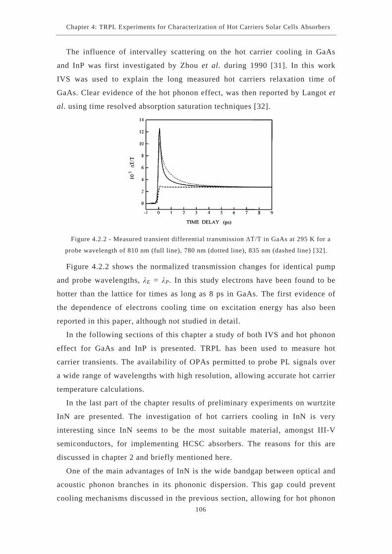
Chapter 4: TRPL Experiments for Characterization of Hot Carriers Solar Cells Absorbers
The influence of intervalley scattering on the hot carrier cooling in GaAs
and InP was first investigated by Zhou et al. during 1990 [31]. In this work
IVS was used to explain the long measured hot carriers relaxation time of
GaAs. Clear evidence of the hot phonon effect, was then reported by Langot et
al. using time resolved absorption saturation techniques [32].
Figure 4.2.2 - Measured transient differential transmission T/T in GaAs at 295 K for a
probe wavelength of 810 nm (full line), 780 nm (dotted line), 835 nm (dashed line) [32].
Figure 4.2.2 shows the normalized transmission changes for identical pump
and probe wavelengths, E = P. In this study electrons have been found to be
hotter than the lattice for times as long as 8 ps in GaAs. The first evidence of
the dependence of electrons cooling time on excitation energy has also been
reported in this paper, although not studied in detail.
In the following sections of this chapter a study of both IVS and hot phonon
effect for GaAs and InP is presented. TRPL has been used to measure hot
carrier transients. The availability of OPAs permitted to probe PL signals over
a wide range of wavelengths with high resolution, allowing accurate hot carrier
temperature calculations.
In the last part of the chapter results of preliminary experiments on wurtzite
InN are presented. The investigation of hot carriers cooling in InN is very
interesting since InN seems to be the most suitable material, amongst III-V
semiconductors, for implementing HCSC absorbers. The reasons for this are
discussed in chapter 2 and briefly mentioned here.
One of the main advantages of InN is the wide bandgap between optical and
acoustic phonon branches in its phononic dispersion. This gap could prevent
cooling mechanisms discussed in the previous section, allowing for hot phonon 106
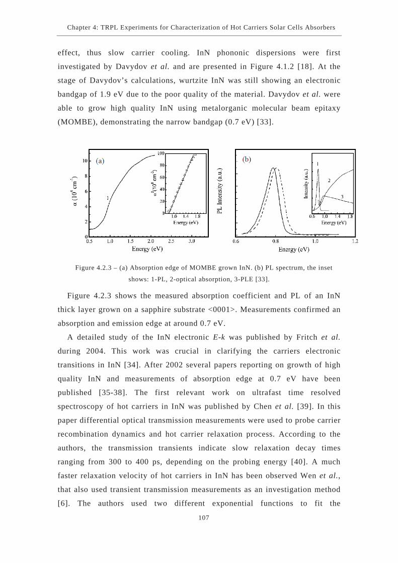
Chapter 4: TRPL Experiments for Characterization of Hot Carriers Solar Cells Absorbers
effect, thus slow carrier cooling. InN phononic dispersions were first
investigated by Davydov et al. and are presented in Figure 4.1.2 [18]. At the
stage of Davydov’s calculations, wurtzite InN was still showing an electronic
bandgap of 1.9 eV due to the poor quality of the material. Davydov et al. were
able to grow high quality InN using metalorganic molecular beam epitaxy
(MOMBE), demonstrating the narrow bandgap (0.7 eV) [33].
Figure 4.2.3 – (a) Absorption edge of MOMBE grown InN. (b) PL spectrum, the inset
shows: 1-PL, 2-optical absorption, 3-PLE [33].
Figure 4.2.3 shows the measured absorption coefficient and PL of an InN
thick layer grown on a sapphire substrate <0001>. Measurements confirmed an
absorption and emission edge at around 0.7 eV.
A detailed study of the InN electronic E-k was published by Fritch et al.
during 2004. This work was crucial in clarifying the carriers electronic
transitions in InN [34]. After 2002 several papers reporting on growth of high
quality InN and measurements of absorption edge at 0.7 eV have been
published [35-38]. The first relevant work on ultrafast time resolved
spectroscopy of hot carriers in InN was published by Chen et al. [39]. In this
paper differential optical transmission measurements were used to probe carrier
recombination dynamics and hot carrier relaxation process. According to the
authors, the transmission transients indicate slow relaxation decay times
ranging from 300 to 400 ps, depending on the probing energy [40]. A much
faster relaxation velocity of hot carriers in InN has been observed Wen et al.,
that also used transient transmission measurements as an investigation method
[6]. The authors used two different exponential functions to fit the
107

Chapter 4: TRPL Experiments for Characterization of Hot Carriers Solar Cells Absorbers
experimental data, representing the cooling process and the carrier
recombination with two different time constants. Carriers cooling time from
1.44 ps to 4.4 ps were reported as results from the fittings depending on the
photoexcited carrier density. The interdependence of the cooling velocity and
the carrier density was observed here for the first time, and was related to the
screening of electron-LO phonon interactions by dense electron plasma [41].
Time constants similar to the ones reported by Wen et al. are observed by
Ascázubi et al., that used time resolved reflectivity measurements [42].
Figure 4.2.4 - Normalized transient transmission change as a function of time delay, for
different photoexcited carrier concentrations. Carrier concentration goes from 5 × 10¹⁸ at a to
1.7 × 10¹⁶ at a’ [6].
Although results from transient absorption experiments give an idea of the
velocity of carrier relaxation, they do not allow relation of the entire hot carrier
energy distribution to the time domain. TRPL, instead, allows probing the
entire luminescent spectrum as a function of time, permitting to measurement
of the energy distribution of electrons and holes. If the photo-emitted spectrum
is known, the hot carrier temperature can be calculated using fitting techniques,
as will be discussed in the next sections.
Results from PL and TRPL experiments on InN have been presented in
recent reports, together with an interesting quantitative study of electron-
phonon and phonon-phonon interaction using ultrafast Raman spectroscopy [7,
43, 44].
Tsen et al. measured the electron-phonon and phonon-phonon interaction
using ultrafast Raman spectroscopy [43]. They observed electron-LO phonon
scattering rates of 5.1 × 10¹³ s-1 and lifetimes of A1(LO) and E1(LO) in the
108

Chapter 4: TRPL Experiments for Characterization of Hot Carriers Solar Cells Absorbers
range between 2.2 ps and 0.25 ps depending on photoexcited carrier density.
The reasons behind the relation between phonon lifetimes and carrier density
are currently not clear and more investigation is needed. However, the electron-
LO phonon scattering rate is much larger compared to values predicted by
theory. This is attributed to the extremely polar nature of InN which strongly
increases the Fröhlich interaction matrix element and is observed also in other
III-V semiconductors. The long LO phonon lifetimes have been recently
confirmed by Jang et al. using TRPL experiments [44]. TRPL allows
observation of a consistent hot phonon effect at carrier densities above 1018 cm-
3, as evidenced by the elongated relaxation transients in Figure 4.2.5.
Figure 4.2.5 – TRPL transients of wurtzite InN at several probe energies [44].
109

Chapter 4: TRPL Experiments for Characterization of Hot Carriers Solar Cells Absorbers
110
4.3 Probing ultrafast dynamic processes in
semiconductors
Over the last thirty years remarkable improvements in ultrafast carrier
spectroscopy have been achieved. The interest was driven both by fundamental
physics research and the need for faster and better performing microelectronic
devices. The study of the relaxation of excited non-equilibrium carriers in
semiconductors is nowadays a popular topic of research. This is also a crucial
matter to identify potential good absorber materials for HCSCs.
With the devolvement of femtosecond lasers and optical parametric
amplifiers it is possible to excite carriers in an extremely short time interval
and successfully probe the material optical properties, such as transmission or
reflection or PL, using a similar laser pulse, often at different wavelength.
Nowadays this is a common type of experiment to investigate ultrafast
processes in semiconductors. The most commonly used techniques are: pump
and probe, optical Kerr gate, up conversion gate and streak camera.
In this chapter the attention will be focused on pump and probe techniques,
in particular on TRPL.
4.3.1 Time resolved photoluminescence using up-conversion
technique
PL is a well known and widely used technique to investigate semiconductor
properties. PL has been presented in chapter 3 for investigation of single layer
QDs properties. In this chapter TRPL has been used to study hot carriers
relaxation transients in III-V semiconductors. TRPL has been used in pump-
probe configuration. In this setup an extremely short laser pulse is separated
into two different pulses the “pump” and the “probe” and an optical delay T is
placed between them. The pump pulse excites the sample generating a PL
signal. A probe pulse, which is referred to as “gate” pulse in this configuration,
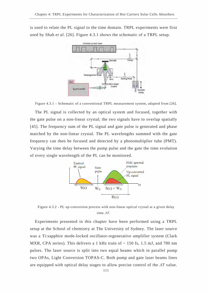
Chapter 4: TRPL Experiments for Characterization of Hot Carriers Solar Cells Absorbers
is used to relate the PL signal to the time domain. TRPL experiments were first
used by Shah et al. [26]. Figure 4.3.1 shows the schematic of a TRPL setup.
Figure 4.3.1 – Schematic of a conventional TRPL measurement system, adapted from [26].
The PL signal is collected by an optical system and focused, together with
the gate pulse on a non-linear crystal; the two signals have to overlap spatially
[45]. The frequency sum of the PL signal and gate pulse is generated and phase
matched by the non-linear crystal. The PL wavelengths summed with the gate
frequency can then be focused and detected by a photomultiplier tube (PMT).
Varying the time delay between the pump pulse and the gate the time evolution
of every single wavelength of the PL can be monitored.
Figure 4.3.2 - PL up-conversion process with non-linear optical crystal at a given delay
time T.
Experiments presented in this chapter have been performed using a TRPL
setup at the School of chemistry at The University of Sydney. The laser source
was a Ti:sapphire mode-locked oscillator-regenerative amplifier system (Clark
MXR, CPA series). This delivers a 1 kHz train of ~ 150 fs, 1.5 mJ, and 780 nm
pulses. The laser source is split into two equal beams which in parallel pump
two OPAs, Light Conversion TOPAS-C. Both pump and gate laser beams lines
are equipped with optical delay stages to allow precise control of the T value. 111

Chapter 4: TRPL Experiments for Characterization of Hot Carriers Solar Cells Absorbers
112
In general the delay stage on the pump line is kept at a fixed position whereas
the stage on the gate line is electronically controlled by a software interface, to
allow measurements of signal transients with a ps resolution.
The visible-OPA produces signal and idler beams that are tunable from 1020
nm, to 1640 nm, and 1470 nm, to 2600 nm respectively. Two successive non
linear crystals (LBO) allow for second and fourth harmonic generation of the
amplified signal and idler, as well as sum frequency mixing with the remaining
portion of the pump pulse (780 nm). This system configuration provides 150 fs
pulses with tunable wavelength over a range from 256 nm (4.84 eV) to 2.6 m
(0.48 eV). The deep-UV-OPA uses a similar optical arrangement to produce an
independently tunable beam over a wavelength range from 187 nm (6.6 eV) to
2.6 m (0.48 eV) and is used to generate the pump pulse. The pump beam is
focused by a 1000 mm focal length lens and the beam profile, considered to be
gaussian, is measured to be 600 m in diameter (FWHM). The
photoluminescence signal from the sample is collected and focused on a 1 mm
beta barium borate (BBO) crystal, the visible-OPA beam, acting as a gate, is
directed and focused on the same spot on the BBO. The up-converted signal is
detected through filters and a double monochromator to eliminate background
light. The signal is then detected with a low noise Bi-PMT. The group velocity
mismatch between the pump and the luminescence wavelength is always less
than 50 fs/mm in BBO and the pulse duration is 150 fs, yielding an overall
temporal resolution of around 200 fs. The carrier concentration of the excited
samples has been determined considering the number of excited carriers (one
excited electron per incoming photon) in a volume limited by the beam spot
size and a depth 1/ ( ) (where ( ) is the absorption coefficient at excitation
wavelength ) in the material.

Chapter 4: TRPL Experiments for Characterization of Hot Carriers Solar Cells Absorbers
Figure 4.3.3 – Simplified schematics of the time resolved photoluminescence system at the
femtosecond laboratory, University of Sydney, Faculty of Chemical Sciences.
113

Chapter 4: TRPL Experiments for Characterization of Hot Carriers Solar Cells Absorbers
114
4.4 Comparison of hot carrier cooling gallium
arsenide and indium phosphide
Hot carrier relaxation in bulk GaAs and InP has been investigated by TRPL.
One of the aims of this work is to establish the role of the hot phonon effect in
carrier cooling for InP. The two semiconductors have similar electronic band
gaps (EG_GaAs = 1.43 eV, EG_InP = 1.35 eV), but quite different phononic band
gaps. In particular InP has a wider phononic bandgap, hence is expected to
show a slower carrier cooling.
Several excitation wavelengths have been used to investigate the effects of
satellite valley scattering on the relaxation. For an initial carrier concentration
of 8 × 1019 cm-3, a very broad emission spectrum which extends from the band
gap energy to energies above the pump has been measured both for GaAs and
InP, demonstrating the extremely fast interactions of carriers at very early
times (~ 100 fs) after the laser excitation. Full PL spectra have been simulated
and fitted with experimental data to extract the hot carrier temperature Te as a
function of time for both GaAs and InP. The difference between the GaAs and
InP PL decay rates depends on the excitation wavelength, proving the role
played by the X and L valleys in GaAs and the influence of IVS on the cooling
process. The temperature evolution is also related to the excitation wavelength.
Thermalisation of hot carriers in InP is always slower than in GaAs when
excitation energy below the satellite valleys thresholds is used, providing
evidence of a hot phonon effect in bulk InP.
In order to investigate and differentiate the influence of the hot phonon
effect and IVS on the hot carrier cooling rate, the evolution of the PL signal
has been studied for different pump wavelengths. Three different excitation
energies have been used to excite carriers in the different conduction band
valleys of the two materials. A schematic representation of the band structures
is depicted in Figure 4.4.1. E1 = 1.7 eV, which is below the IVS threshold for
GaAs and InP, E2 = 1.88 eV, which is below the L valley for InP but above the
L valley for GaAs and E3 = 2.4 eV, which pumps electrons above the L and X
valley for both materials.

Chapter 4: TRPL Experiments for Characterization of Hot Carriers Solar Cells Absorbers
Figure 4.4.1 - Schematic representation of GaAs (dot) and InP (dash) electronic band
structure. The different pump energies used for investigation are shown [46].
4.4.1 Hot carriers cooling
Figure 4.4.2 shows the evolution of the PL spectrum of GaAs and InP, for a
1.7 eV (730 nm) pump pulse, at a carrier density of 8.5 × 1019 cm-3. This value
of carrier density in the absorber is chosen because in a required range for
HCSC operating at maximum power point under full concentration [47].
Considering an ultrafast carrier-carrier scattering rate (see chapter 2), a hot
Fermi distribution can be assumed for photoexcited carriers. This assumption is
supported by the initial very broad PL spectrum (few ps) observed both in
GaAs and InP, Figure 4.4.2 [8, 9]. The energy distribution of the spectra
narrows down and the peaks shift towards the band edge due to carrier cooling,
Figure 4.4.2 (e,f). Figure 4.4.2 (c,d) shows the normalized PL transients for
some particular energies. It is evident that highly energetic states empty much
faster than states closer to the band edges and that IVS has a role only at the
very early stage of the cooling process. The PL signal below the bandgap can
be attributed to blurring of the bandgap energy states at high photoexcitation
regimes [48].
115

Chapter 4: TRPL Experiments for Characterization of Hot Carriers Solar Cells Absorbers
Figure 4.4.2 -3D evolution of PL spectra versus time (1.70 eV pump) for (a) GaAs and (b)
InP. The carrier concentration is 8.5 × 1019 cm-3. Transient PL spectra for different
wavelengths in (c) GaAs and (d) InP. Insets show the band edge PL emission. PL spectra for
different delay time in (e) GaAs and (f) InP.
Figure 4.4.3 shows the PL signal time constant, fitted using a simple
exponential function, versus the emission wavelength. Using a 730 nm (1.7 eV)
pump, no significant interaction of hot carriers with side valleys has been
observed. The L valley for GaAs, in fact, has a threshold of 725 nm (1.71 eV).
116

Chapter 4: TRPL Experiments for Characterization of Hot Carriers Solar Cells Absorbers
Figure 4.4.3 - Fitted PL signal decay constant as a function of wavelength for different
pump wavelengths, (a) 730 nm, (b) 660 nm, (c) 515 nm. Carrier concentration is always 8.5 ×
1019 cm-3, signals have been fitted using a single exponential [46].
117

Chapter 4: TRPL Experiments for Characterization of Hot Carriers Solar Cells Absorbers
4.4.2 Hot phonon effect in gallium arsenide and indium
phosphide
Figure 4.4.4 shows the phonon dispersion relations for GaAs and InP [49,
50]. The energy of the zone centre LTO phonon for InP is 10 THz and the
maximum LA phonon energy, at the zone edge, is 4.8 THz and 4.4 THz, for the
X and L directions respectively. These LA energies are smaller than half of the
LTO phonon energy; hence they are not sufficient for the decay of the LTO
phonon by Klemens mechanism. This suggests that Klemens mechanism would
be partially suppressed. However, the minimum energy of optical phonons is at
8.7 THz at the point in the X direction. This is less than twice the energy of
the maximum LA phonon, so in this case Klemens decay of the optical phonon
would be allowed.
Figure 4.4.4 - Calculated phonon dispersion relations for (a) GaAs and (b) InP [46].
118

Chapter 4: TRPL Experiments for Characterization of Hot Carriers Solar Cells Absorbers
119
The zone centre LTO phonon is however able to undergo Ridley decay by
emission of a LO phonon, at 8.7 THz to the point, and simultaneously a 1.3
THz TA phonon, to the point in the L direction. This balances both energy
and momentum and is an extra allowed transition to the more usual Ridley
decay to a TO and a LA phonon described in Section 4.1. The degeneracy of
LO and TO modes at zone center means that no specific translation is preferred
in the decay and either a TO or a LO phonon can be emitted, provided it is
matched by the appropriate LA or TA phonon of correct energy and
momentum. This zone center LTO degeneracy arises because of the cubic
zincblende structure of InP, which strictly gives zero dispersion at zone center,
and the relatively low polarity of the InP bond, which reduces the tendency for
splitting of LO and TO modes at zone center.
The effect on carrier cooling of the much larger phononic gap in InP, as
compared to GaAs, is clearly visible in Figure 4.4.5 and Figure 4.4.3, with
illumination at 730 nm. This is below the energy necessary for IVS, thus zone
centre valley interactions dominate in both InP and GaAs. The longer PL
lifetime for InP at all wavelengths, Figure 4.4.3(a), and the higher effective
carrier temperature at all times, Figure 4.4.5(a), clearly indicates slower carrier
cooling in InP. This suggests that the suppression of LTO decay by Klemens
mechanism enhances the hot phonon effect and slows down carrier relaxation.
For 8.7 THz optical phonons, at the point, the Klemens mechanism is allowed
and hence the decay would remain unrestricted. The important consideration in
the overall enhancement of the hot phonon effect is the distribution of optical
phonon momenta.

Chapter 4: TRPL Experiments for Characterization of Hot Carriers Solar Cells Absorbers
Figure 4.4.5 - Carriers temperature as a function of time after excitation with (a) 730 nm,
(b) 660 nm, (c) 515 nm pump pulses.
The distribution of momenta of the emitted optical phonons is strongly
peaked near zone center because the Fröhlich interaction in polar compound
semiconductors only allows emission of small wavevector phonons. In fact, the
long range electronic oscillations of oppositely charged atoms, set-up by the
phonon emission, create a strong coulombic repulsion of phonons with any
translational momentum [16]. The dependence of the phonon distribution on
wavenumber, q, varies as q-2. A further effect of the Fröhlich emission of low
wavenumber phonons occurs for higher energy electrons, in the region of the
120

Chapter 4: TRPL Experiments for Characterization of Hot Carriers Solar Cells Absorbers
121
conduction band, in which the assumption of parabolicity of the E-k
relationship is no longer valid. This non-parabolicity arises from hybridization
of s and p states and determines the band structure of higher bands [51]. As the
long range Coulomb effects determine emission of only low wavenumber
phonons, it is results very difficult for high energy electrons to emit a phonon
conserving both energy and momentum. This makes the emission of very low
energy acoustic phonons, close to zone center, the only available scattering
event. A large number of these events is required for the hot electron to lose a
significant amount of energy. The probability of emitting such a large number
of acoustic phonons is limited. The result is the creation of a large population
of optical phonons or, in other words, a hot phonon effect. This implies that the
gap between optical and acoustic phonon branches in InP is large enough to
prevent Klemens decay, enhance the hot phonon effect and produce the
observed slower carrier cooling.
However, as discussed above the alternative Ridley mechanism can still
occur for decay of low wavenumber LTO phonons. In InP this will be followed
by a rapid decay of LO phonons from the point via an off-zone centre
Klemens decay as discussed above. This is a two stages process, involving five
phonons and hence should have a lower probability compared to direct
Klemens decay of the LTO phonon.
Some result indicates that the overall rate of the Ridley/Klemens decay is
dominated by the slow Ridley part, which is a factor of ten times slower than
the Klemens part due primarily to the lower final DOS for the Ridley transition
[52]. This is only partially applicable in the InP case discussed here, as the
calibration of the phonon dispersions differs significantly, but it is indicative of
how Ridley decay can reduce the overall rate in a two-step decay process.
It can be concluded that the complex Ridley/Klemens decay required in InP
for decay of zone-center phonons as compared to the many routes allowed for
the rapid one step Klemens decay of optical phonons in GaAs, does explain the
observed slowed carrier cooling in the former by an enhancement of the hot
phonon effect. Nevertheless it is also valid to state that a wider phonon gap that
is sufficient to block both Klemens and Ridley decay, or to block the Klemens

Chapter 4: TRPL Experiments for Characterization of Hot Carriers Solar Cells Absorbers
decay of Ridley decayed phonons, should enhance the hot phonon effect further
and would be expected to slow carrier cooling to a greater extent.
4.4.3 Inter-valley scattering of hot carriers in gallium
arsenide and indium phosphide
Figure 4.4.5 (b) and (c) clearly show that with the inclusion of the L valley
of GaAs, the rate of cooling in the first 10 ps to 15 ps is significantly lower in
GaAs, suggesting an efficient IVS process in GaAs. This can be explained by
examining the electronic band structures of both semiconductors and the
Fröhlich interaction within the framework of Fermi’s Golden Rule [53]. For a
side valley (X, L) electron scattered into the valley, with momentum
conservation fulfilled by the emission of an off-center LO phonon, the
transition probability can be written as in (4.4.1):
,
2
, ,2 finfinih oscvLX (4.4.1)
The electron initial state (ini) is the L or X side valley, the electron final
state (fin) is given by an unoccupied valley state convoluted with the LO
phonon with an appropriate momentum to allow a X or L transition.
The oscillator strength of the transition (fosc), which describes the coupling
between initial and final state, is proportional to the Fröhlich interaction ( FRÖ)
[54].
For InP the Fröhlich interaction is larger than GaAs ( FRÖ_InP = 0.15 [55],
FRÖ_GaAs = 0.068 [56]) due to its more polar nature and lower LO phonon
frequency, yielding a higher oscillator strength for IVS [57].
The PL lifetime of GaAs is significantly shorter if no side valleys are
occupied despite its lower Fröhlich constant. This is a clear indication that the
wide phononic band gap of InP delays carrier cooling by slowing the decay of
optical phonons. When the pump energy exceeds the energy threshold for
transfer into satellite valleys, the PL lifetime of GaAs is equal or even exceeds
the values of InP, as evidenced Figure 4.4.3. This confirms the dominance of
FRÖ in the IVS process and appears to be plausible. Without Fröhlich
interaction, only a very small phononic coupling, between electrons in the side 122
Chapter 4: TRPL Experiments for Characterization of Hot Carriers Solar Cells Absorbers
123
valleys and unoccupied electronic states in the main valley exists, due to
electrons to acoustic phonon scattering. Acoustic phonons do not couple
readily to electrons due to their low electromagnetic moment. The higher LA
L intervalley deformation potential of GaAs does thereby contribute to IVS
only as a second order effect [58]. The respective electronic DOS appears to be
not as influential as FRÖ. This is due to the convolution product of the
electronic DOS of the side and main valleys, which only changes significantly
if both DOS are very small or large. In other words, the bottleneck of IVS is
given by the Fröhlich interaction. GaAs has thus a slower IVS mechanism and
can store hot electrons in the side valleys for a longer time as compared to InP.

Chapter 4: TRPL Experiments for Characterization of Hot Carriers Solar Cells Absorbers
124
4.5 Time resolved photoluminescence of hot
carriers in indium nitride layers
InN is a very good candidate, amongst others III-V semiconductors, to
implement a HCSC absorber. The reasons for this have been discussed in
Section 4.2. In summary, InN has a small electronic band gap (0.7 eV) for
better light absorption and, at the same time, it has a wide gap between
acoustic and optical branches in its phonon dispersion characteristic, allowing
slower thermalisation of hot carriers by hot phonon effect [18, 34]. Time
resolved experiments have reported hot carriers relaxation time longer than
theoretical calculations [39, 42, 59]. This prolonged hot carriers lifetime is
most probably due to hot phonon effect, thus minimization of the losses rate
via Fröhlich interaction under high photoexcitation [32, 60].
4.5.1 Preliminary results on hot carriers cooling in wurtzite
indium nitride
To investigate on the actual relaxation velocity of hot carriers in InN, TRPL
experiments have been performed on InN thick layers.
Samples have been deposited using plasma assisted molecular beam epitaxy,
by Dr. Y. Wen and Dr. C. Chen at the University of Taipei, on Sapphire
<0001> substrate using two GaN nucleation layers to optimize crystal
properties and minimize defects. Figure 4.5.1 shows the layered structure of the
examined sample and a SEM image of the sample surface. The measured
carrier concentration was around 1.5 × 1018 cm-3. Carrier mobilities were
measured to be around 2000 cm2/Vs.

Chapter 4: TRPL Experiments for Characterization of Hot Carriers Solar Cells Absorbers
Figure 4.5.1 - (a) InN sample layer structure. GaN nucleation layers are used to optimize
InN crystal structure. (b) SEM image of the investigated InN sample.
The samples have been excited using the pulsed laser described in the
previous sections, with an energy of 1.1 eV. The beam size was 0.8 mm and the
energy per pulse was 35 J. The gate wavelength used was 780 nm (1.59 eV),
which is the unmodified Ti:sapphire wavelength, thus the one with the highest
power. The up-converted wavelengths detected by the PMT were in the range
480 nm – 522 nm. Measurements have been performed at room temperature.
The collected raw data have been corrected for the cathode radiant
sensitivity of the PMT and pre fitted using weighted exponential functions, as
shown in Figure 4.5.2.
125

Chapter 4: TRPL Experiments for Characterization of Hot Carriers Solar Cells Absorbers
Figure 4.5.2 - 3D surfaces of collected and fitted TRPL data for bulk InN.
The figure is a three dimensional representation of PL as a function of time
for all the probed wavelengths. It can be observed that the PL sharply rises
when the carriers are photo-excited by the laser pulse. The fast decay of the PL
shows the thermalisation of carriers towards respective band edges. The decay
is faster for highly energetic carriers compared to carriers closer to the bandgap
as also observed for GaAs and InP. Thus the carrier population quickly
accumulates towards band edges during the thermalisation process. In InN the
thermalisation is most probably due to interaction of highly energetic electrons
and holes with LO phonons [6].
To investigate the velocity of the carrier cooling process, the effective
temperature of the carrier population has been calculated fitting the high
energy tail of the PL spectrum for every single time during the cooling
transient [44]. The PL has been fitted assuming that carriers assume a
Boltzmann-like distribution in a femtosecond time scale, as discussed at the
126

Chapter 4: TRPL Experiments for Characterization of Hot Carriers Solar Cells Absorbers
beginning of this chapter. Equation (4.5.1) shows the expression used to
calculate carrier temperature.
CB
G
TkEL exp)()( 2 (4.5.1)
L( ) represents the measured PL intensity at energy , ( ) is the measured
sample absorption coefficient, EG is the InN energy gap (0.7 eV), and kB is the
Boltzmann constant. TC is the fitted parameter and represents the hot carrier
temperature. Figure 4.5.3 shows the carrier temperature transient, which
follows quite well an exponential behaviour (dashed line – fit).
Figure 4.5.3 - Carrier relaxation curves for InN. The photoexcited carrier density is 1.5 ×
1019 cm-3. The blue dashed curve is a single exponential fitting.
The fitting of the calculated temperature data has been performed using a
single exponential as in equation (4.5.2).
KtCtTTH
exp)( (4.5.2)
Here TH represents the carriers thermalisation time constant, whereas C and
K are two constant parameters. The fitted value for TH is 7 ps. The relatively
long cooling constant can be attributed to hot phonon effect due to the long
lifetime of the A1(LO) phonon [7, 61], although this result is still controversial
[6]. This hot carrier relaxation velocity is still faster than the value previously
used in chapter 2 (100 ps) to evaluate limiting efficiency of a HCSC with an
InN absorber. However, it has been demonstrated that, for InN, the carrier
cooling velocity is strictly related to the quality of the material and slower
127

Chapter 4: TRPL Experiments for Characterization of Hot Carriers Solar Cells Absorbers
128
carrier cooling constants, compared to the ones calculated in this chapter, have
been reported in the literature [40].
It has to be highlighted that the growth of ultra high quality wurtzite InN
remains still a very complicated and expensive task, due to the involvement of
MBE growth technique [62].

Chapter 4: TRPL Experiments for Characterization of Hot Carriers Solar Cells Absorbers
129
4.6 Summary
In this chapter time resolved photoluminescence experiments have been
performed on several III-V bulk semiconductors in order to investigate the
factors that influence hot carrier cooling processes. The possibility of probing
hot carrier transients with picosecond accuracy allows study of the relations
between materials phononic dispersion curves and velocity of carrier cooling.
This is very useful to screen potential candidate materials for hot carrier solar
cells absorbers and, at the same time, is crucial for the designing of new
nanostructured absorbers based on superlattices.
In the first part of the chapter the topic of hot carriers relaxation in
semiconductors is introduced and several significant papers on the
investigation of ultrafast phenomena in semiconductors are presented and
discussed. In addition an introduction of ultrafast measurements and systems is
given; this includes a presentation of up-conversion time resolved
photoluminescence techniques.
In the second part of the chapter results on the influence of the hot phonon
effect and IVS on the hot carrier cooling rate in bulk GaAs and InP is
presented. Experiments have been performed using femtosecond luminescence
spectroscopy with different pump energies. Under high carrier concentration, a
longer hot carrier cooling transient has been observed in InP as compared to
GaAs, when electrons energy is not high enough to access satellite valleys,
proving the influence of the hot phonon effect on the carrier relaxation. A clear
indication that the wide phononic bandgap of InP slows carrier cooling, by
minimizing the decay of zone center optical phonons, has also been observed.
This is explained by the stronger Fröhlich interaction for InP as compared to
GaAs. It was found that the Fröhlich interaction is not the limiting factor for
electron cooling in the valley. Photoluminescence at wavelengths shorter
than the excitation of the ground valley has also been presented, demonstrating
that spectral broadening occurs during the early stage of the thermalisation
process. It has also been shown that intervalley scattering decreases the hot
carrier cooling rate into the main valley. The Fröhlich interaction appears to

Chapter 4: TRPL Experiments for Characterization of Hot Carriers Solar Cells Absorbers
130
dominate intervalley scattering, resulting in slowing of carrier cooling in GaAs
by storing hot electrons in side valleys.
The last part of the chapter is dedicated to the investigation of hot carrier
cooling in bulk wurtzite InN samples. Theoretically InN would be the best
candidate, amongst bulk III-V semiconductors, to realize a hot carrier solar cell
absorber. Time resolved photoluminescence experiments have demonstrated
that carriers can be excited above 2000 K in InN using laser pulses of 35 J at
1.1 eV. In the analysed sample, carrier temperature decays towards lattice
temperature with a time constant of around 7 ps, which demonstrates the
presence of hot phonon effect in InN. Although this value is reasonably high, it
is still below the minimum acceptable value for realizing an InN based hot
carriers solar cell absorber. Slower thermalisation constants can be obtained
improving the quality of the material, but this involves demanding deposition
techniques.

Chapter 4: TRPL Experiments for Characterization of Hot Carriers Solar Cells Absorbers
131
4.7 Bibliography
1. Aliberti, P., Y. Feng, Y. Takeda, S.K. Shrestha, M.A. Green, and G.J.
Conibeer, Investigation of theoretical efficiency limit of hot carrier
solar cells with bulk InN absorber. Journal of Applied Physics, 2010.
108(9): p. 094507-10.
2. Conibeer, G., D. König, M.A. Green, and J.-F. Guillemoles, Slowing of
carrier cooling in hot carrier solar cells. Thin Solid Films, 2008.
516(20): p. 6948-6953.
3. Jang, D.J., G.T. Lin, M.E. Lee, C.L. Wu, C.L. Hsiao, and L.W. Tu,
Carrier dynamics and intervalley scattering in InN. Optical Materials,
2009. 31(12): p. 1857-1859.
4. Luque, A. and A. Marti, Electron-phonon energy transfer in hot-carrier
solar cells. Solar energy materials and solar cells, 2010. 94(2): p. 287-
296.
5. Wen, X.M., L. Van Dao, P. Hannaford, E.C. Cho, Y.H. Cho, and M.A.
Green, Ultrafast Transient Grating Spectroscopy in Silicon Quantum
Dots. Journal of Nanoscience and Nanotechnology, 2009. 9(8): p. 4575-
4579.
6. Wen, Y.C., C.Y. Chen, C.H. Shen, S. Gwo, and C.K. Sun, Ultrafast
carrier thermalization in InN. Applied Physics Letters, 2006. 89(23): p.
232114.
7. Yang, M.D., Y.P. Chen, G.W. Shu, J.L. Shen, S.C. Hung, G.C. Chi, T.Y.
Lin, Y.C. Lee, C.T. Chen, and C.H. Ko, Hot carrier photoluminescence
in InN epilayers. Applied Physics a-Materials Science & Processing,
2008. 90(1): p. 123-127.
8. Elsaesser, T., J. Shah, L. Rota, and P. Lugli, Femtosecond luminescence
spectroscopy of carrier thermalization in GaAs and InP. Semiconductor
Science and Technology, 1992. 7(3B): p. 144-147.
9. Shah, J., Radiative recombination from photoexcited hot carriers in
GaAs. Physical review letters, 1969. 22(24): p. 1304-1307.
Chapter 4: TRPL Experiments for Characterization of Hot Carriers Solar Cells Absorbers
132
10. Green, M.A., Third generation photovoltaics: advanced solar
conversion. 2003: Springer-Verlav.
11. Conibeer, G., N. Ekins-Daukes, J.-F. Guillemoles, D. König, E. Cho,
C.W. Jiang, S.K. Shrestha, and M.A. Green, Progress on hot carrier
cells. Solar energy materials and solar cells, 2009. 93(6-7): p. 713-719.
12. Klemens, P.G., Anharmonic Decay of Optical Phonons. Physical
Review, 1966. 148(2): p. 845.
13. Nozik, A.J., C.A. Parsons, D.J. Dunlavy, B.M. Keyes, and R.K.
Ahrenkiel, Dependence of hot carrier luminescence on barrier thickness
in GaAs/AlGaAs superlattices and multiple quantum wells. Solid State
Communications, 1990. 75(4): p. 297-301.
14. Westland, D.J., J.F. Ryan, M.D. Scott, J.I. Davies, and J.R. Riffat, Hot
carrier energy loss rates in GaInAs/InP quantum wells. Solid-State
Electronics, 1988. 31(3-4): p. 431-434.
15. Conibeeer, G., J.-F. Guillemoles, D. König, and M.A. Green, Phononic
Band Gap Engineering for Hot Carrier Solar Cell Absorbers, in 21st
European Photovoltaic and Solar Energy Conference. 2006: Dresden. p.
90.
16. Othonos, A., Probing ultrafast carrier and phonon dynamics in
semiconductors. Journal of Applied Physics, 1998. 83(4): p. 1789-1830.
17. Rydley, B.K., The LO phonon lifetime in GaN. J. Phys.: Condens.
Matter, 1996. 8: p. L511-L514.
18. Davydov, V.Y., V.V. Emtsev, I.N. Goncharuk, A.N. Smirnov, V.D.
Petrikov, V.V. Mamutin, V.A. Vekshin, S.V. Ivanov, M.B. Smirnov, and
T. Inushima, Experimental and theoretical studies of phonons in
hexagonal InN. Applied Physics Letters, 1999. 75(21): p. 3297-3299.
19. Butcher, P.M., Gunn effect. Reports on Progress in Physics, 1967. 30: p.
97.
20. Herbert, D.C., Electron-phonon interaction and inter-valley scattering
in semiconductors. Journal of Physics C-Solid State Physics, 1973.
6(18): p. 2788-2810.
21. Shah, J., R.C.C. Leite, and J.F. Scott, Photoexcited hot LO phonons in
GaAs. Solid State Communications, 1970. 8(14): p. 1089.

Chapter 4: TRPL Experiments for Characterization of Hot Carriers Solar Cells Absorbers
133
22. Shah, J., Hot electrons and phonons under high intensity photoexcitation
of semiconductors. Solid-State Electronics, 1978. 21(1): p. 43-50.
23. Leheny, R.F., J. Shah, R.L. Fork, C.V. Shank, and A. Migus, Dynamics
of hot carrier cooling in photoexcited GaAs. Solid State
Communications, 1979. 31(11): p. 809-813.
24. Shah, J., Investigation of hot carrier relaxation with picosecond laser-
pulses. Journal De Physique, 1981. 42(NC7): p. 445-462.
25. Block, D., J. Shah, and A.C. Gossard, Femtosecond luminescence
measurements in GaAs. Solid State Communications, 1986. 59(8): p.
527-531.
26. Shah, J., T.C. Damen, B. Deveaud, and D. Block, Subpicosecond
luminescence spectroscopy using sum frequency generation. Applied
Physics Letters, 1987. 50(19): p. 1307-1309.
27. Shah, J., B. Deveaud, T.C. Damen, W.T. Tsang, A.C. Gossard, and P.
Lugli, Determination of intervalley scattering rates in GaAs by
subpicosecond luminescence spectroscopy. Physical review letters,
1987. 59(19): p. 2222-2225.
28. Becker, P.C., H.L. Fragnito, C.H.B. Cruz, J. Shah, R.L. Fork, J.E.
Cunningham, J.E. Henry, and C.V. Shank, Femtosecond Intervalley
scattering in GaAs. Applied Physics Letters, 1988. 53(21): p. 2089-
2090.
29. Shah, J., Ultrafast luminescence spectroscopy using sum frequency
generation. Ieee Journal of Quantum Electronics, 1988. 24(2): p. 276-
288.
30. Shah, J., Ultrafast studies of carrier relaxation in semiconductors and
their microstructures. Superlattices and Microstructures, 1989. 6(3): p.
293-302.
31. Zhou, X.Q., U. Lemmer, K. Seibert, G.C. Cho, W. Kutt, K. Wolter, and
H. Kurz, Subpicosecond dynamics of hot carrier relaxation in InP and
GaAs, in Applications of Ultrashort Laser Pulses in Science and
Technology, A. Antonetti, Editor. 1990, Spie - Int Soc Optical
Engineering: Bellingham. p. 166-176.

Chapter 4: TRPL Experiments for Characterization of Hot Carriers Solar Cells Absorbers
134
32. Langot, P., N. Del Fatti, D. Christofilos, R. Tommasi, and F. Vallée,
Femtosecond investigation of the hot-phonon effect in GaAs at room
temperature. Physical Review B, 1996. 54(20): p. 14487.
33. Davydov, V.Y., A.A. Klochikhin, R.P. Seisyan, V.V. Emtsev, S.V.
Ivanov, F. Bechstedt, J. Furthmüller, H. Harima, A.V. Mudryi, J.
Aderhold, O. Semchinova, and J. Graul, Absorption and emission of
hexagonal InN. Evidence of narrow fundamental band gap. Physica
status solidi (b), 2002. 229(3): p. r1-r3.
34. Fritsch, D., H. Schmidt, and M. Grundmann, Band dispersion relations
of zinc-blende and wurtzite InN. Physical Review B, 2004. 69(16): p.
165204.
35. Wu, J., W. Walukiewicz, K.M. Yu, J.W. Ager, E.E. Haller, H. Lu, W.J.
Schaff, Y. Saito, and Y. Nanishi, Unusual properties of the fundamental
band gap of InN. Applied Physics Letters, 2002. 80(21): p. 3967-3969.
36. Cimalla, V., J. Pezoldt, G. Ecke, R. Kosiba, O. Ambacher, L. Spiess, G.
Teichert, H. Lu, and W.J. Schaff, Growth of cubic InN on r-plane
sapphire. Applied Physics Letters, 2003. 83(17): p. 3468-3470.
37. Bagayoko, D. and L. Franklin, Density-functional theory band gap of
wurtzite InN. Journal of Applied Physics, 2005. 97(12): p. 123708-5.
38. Matsuoka, T., Progress in nitride semiconductors from GaN to InN-
MOVPE growth and characteristics. Superlattices and Microstructures,
2005. 37(1): p. 19-32.
39. Chen, F., A.N. Cartwright, H. Lu, and W.J. Schaff, Time-resolved
spectroscopy of recombination and relaxation dynamics in InN. Applied
Physics Letters, 2003. 83(24): p. 4984-4986.
40. Chen, F., A.N. Cartwright, H. Lu, and W.J. Schaff, Ultrafast carrier
dynamics in InN epilayers. Journal of Crystal Growth, 2004. 269(1): p.
10-14.
41. Collet, J.H., Dynamical screening in the cooling theory of high-density
electron-hole plasmas. Physical Review B, 1989. 39(11): p. 7659-7665.
42. Ascazubi, R., I. Wilke, S.H. Cho, H. Lu, and W.J. Schaff, Ultrafast
recombination in Si-doped InN. Applied Physics Letters, 2006. 88(11):
p. 112111-3.

Chapter 4: TRPL Experiments for Characterization of Hot Carriers Solar Cells Absorbers
135
43. Tsen, K.T. and D.K. Ferry, Studies of electron-phonon and phonon-
phonon interactions in InN using ultrafast Raman spectroscopy. Journal
of Physics-Condensed Matter, 2009. 21(17): p. 174202-7.
44. Jang, D.J., G.T. Lin, C.L. Wu, C.L. Hsiao, L.W. Tu, and M.E. Lee,
Energy relaxation of InN thin films. Applied Physics Letters, 2007.
91(9): p. 092108.
45. Mahr, H. and M.D. Hirsch, Optical up-conversion light gate with
picosecond resolution. Optics Communications, 1975. 13(2): p. 96-99.
46. Clady, R., M.J.Y. Tayebjee, P. Aliberti, D. König, N.J. Ekins-Daukes,
G.J. Conibeer, T.W. Schmidt, and M.A. Green, Interplay between the
hot phonon effect and intervalley scattering on the cooling rate of hot
carriers in GaAs and InP. Progress in Photovoltaics: Research and
Applications, 2011: p. n/a-n/a.
47. Takeda, Y., T. Ito, R. Suzuki, T. Motohiro, S.K. Shrestha, and G.
Conibeer, Impact ionization and Auger recombination at high carrier
temperature. Solar energy materials and solar cells, 2009. 93(6-7): p.
797-802.
48. Christianen, P.C.M. and H.J.A. Bluyssen, The effect of stimulated-
emission on the cooling rate of hot carriers in GaAs. Physica B-
Condensed Matter, 1995. 204(1-4): p. 325-331.
49. Borcherds, P.H., G.F. Alfrey, D.H. Saunderson, and A.D.B. Woods,
Phonon dispersion curves in Indium-Phosphide. Journal of Physics C-
Solid State Physics, 1975. 8(13): p. 2022-2030.
50. Dorner, B. and D. Strauch, Phonon-dispersion sheets and group
velocities in GaAs. Journal of Physics-Condensed Matter, 1990. 2(6): p.
1475-1483.
51. Collins, C.L. and P.Y. Yu, Generation of nonequilibrium optical
phonons in GaAs and their application in studying intervalley electron-
phonon scattering. Physical Review B, 1984. 30(8): p. 4501.
52. Conibeeer, G., R. Patterson, L. Huang, J.F. Guillemoles, D. König, S.K.
Shrestha, and M.A. Green, Hot carriers solar cells absorbers, in 23rd
European Photovoltaic and Solar Energy Conference. 2008: Valencia. p.
156-161.

Chapter 4: TRPL Experiments for Characterization of Hot Carriers Solar Cells Absorbers
136
53. Shiff, L.I., Quantum mechanics. Vol. 3. 1968, Auckland: McGraw-Hill.
54. Clady, R., M.J.Y. Tayebjee, P. Aliberti, D. König, N. Ekins-Daukes, G.
Conibeeer, T.W. Schmidt, and M.A. Green, Interplay between Hot
phonon effect and Intervalley scattering on the cooling rate of hot
carriers in GaAs and InP. Progress in Photovoltaics, 2010. ACCEPTED.
55. Helm, M., W. Knap, W. Seidenbusch, R. Lassnig, E. Gornik, R.
Triboulet, and L.L. Taylor, Polaron cyclotron-resonance in n-CdTe and
n-InP. Solid State Communications, 1985. 53(6): p. 547-550.
56. Adachi, S., GaAs, AlAs, and AlXGa1-XAs - material parameters for use in
research and device applications. Journal of Applied Physics, 1985.
58(3): p. R1-R29.
57. Klingshirn, C., Semiconductor optics, ed. S. Press. Vol. 2. 2005,
Heidelberg: Springer Press.
58. Yu, P. and M. Cadorna, Foundamentals of semiconductors: physics and
material properties, ed. S. Press. Vol. 3. 2005, Heidelberg: Springer
Press.
59. Pacebutas, V., G. Aleksejenko, A. Krotkus, J.W. Ager, I.W.
Walukiewicz, H. Lu, and W.J. Schaff, Optical bleaching effect in InN
epitaxial layers. Applied Physics Letters, 2006. 88(19): p. 191109.
60. Sun, C.K., Y.L. Huang, S. Keller, U.K. Mishra, and S.P. DenBaars,
Ultrafast electron dynamics study of GaN. Physical Review B, 1999.
59(21): p. 13535-13538.
61. Tsen, K.T., J.G. Kiang, D.K. Ferry, H. Lu, W.J. Schaff, H.W. Lin, and
S. Gwo, Direct measurements of the lifetimes of longitudinal optical
phonon modes and their dynamics in InN. Applied Physics Letters, 2007.
90(15): p. 152107-3.
62. Bhuiyan, A.G., A. Hashimoto, and A. Yamamoto, Indium nitride (InN):
A review on growth, characterization, and properties. Journal of
Applied Physics, 2003. 94(5): p. 2779-2808.

Chapter 4: TRPL Experiments for Characterization of Hot Carriers Solar Cells Absorbers
137
4.8 Publications
R. Clady, M.J.Y. Tayebjee, P. Aliberti, D. König, N. Ekins-Daukes, G.
Conibeeer, T.W. Schmidt, and M.A. Green, “Interplay between Hot phonon
effect and Intervalley scattering on the cooling rate of hot carriers in GaAs and
InP”, Progress in photovoltaics, 2011.


Chapter 5
DISCUSSION

Chapter 5: Discussion
138
5.1 Introduction
In the first four chapters of this thesis some of the main scientific and
technological aspects related to the development of a HCSC have been
analysed. Although different aspects of the HCSC design have been treated
separately, one of the clear outcomes of this thesis work is that physical and
electrical properties of absorber and ESCs are highly correlated. The
characteristics of ESCs determine requirements of the absorber material and
vice versa, thus the design of a HCSC has to be seen as a single task, where the
properties and structures of the different components have to be engineered
simultaneously.
This chapter has the aim of bringing the contents studied in the thesis into a
single broad picture, discussing the relations between the properties of ESCs
and absorber material together with technological issues related with the
fabrication of a HCSC device. In particular the first part of the chapter is
dedicated to the discussion of the main parameters that determine the final
device performances and how they are cross-linked with each other.
Subsequently the influence of extraction properties of ESCs on the device
performances is analysed. Two different techniques for realization of contacts
are discussed with some references to compatibility of deposition methods of
contacts and absorber. The second part of the chapter is dedicated to the
analysis of different III-V bulk materials and group IV nanostructures that can
potentially be used as absorbers for HCSC. In the last part of the chapter a
possible preliminary design for a prototype of a HCSC is presented with band
diagrams and potential device configuration.

Chapter 5: Discussion
139
5.2 Correlation between important
parameters of a hot carrier solar cell
In chapter 2 the efficiency limits of a HCSC have been studied in relation to
absorber physical, electrical and optical properties for ideal and non-ideal
ESCs. The modelling work demonstrated that the extraction energy level and
the ESCs selectivity are closely related to hot carrier energy distribution into
the absorber. Thus, the ESCs requirements are different according to E-k
dispersion and absorption properties of the absorber. In addition the energy
distribution of the hot carriers is correlated to their thermalisation velocity [1].
A very fast thermalisation rate implies high losses and that the carrier energy
distribution will have its peak closer to the conduction band of the absorber. A
slow thermalisation velocity allows carriers to stay hot for longer periods,
permitting extraction at higher energies, and thus with a smaller energy loss.
The hot carrier relaxation velocity depends on the absorber layer phononic
dispersion relations and carrier density [2]. The carrier density is directly
related to the equilibrium between absorption, emission and extraction of
carriers established at steady state device operation. Absorption and re-
emission of carriers are related to the electronic properties of the absorber, but
also depend on the hot carrier energy distribution or hot carrier effective
temperature [3].
In Figure 5.2.1 the main properties and processes involved in the energy
conversion are shown schematically with the aim of clarifying their first order
interactions.
Chapter 5: Discussion
Figure 5.2.1 – Block diagram of main mechanisms involved in the HCSC energy
conversion.
Results from theoretical modelling discussed in chapter 2 allow the
conclusion that the limiting efficiency of the device is directly proportional to
the carrier cooling constants. In other words, the slower the cooling of the hot
carriers the higher is the maximum achievable efficiency [1, 4].
Thus, as schematically reported in Figure 5.2.2, the design of a hot carrier
cell should start from choosing the material system that offers the best
properties in terms of carrier cooling and absorption of the solar spectrum.
Furthermore realization of a device with this material system has to be
technologically feasible at moderate costs. The technology has to allow design
and realization of ESCs, possibly using the same deposition methods. This
minimizes the chances of having carrier transport problems at interfaces
between absorber layer and ESCs. After the material system has been selected,
the carrier cooling velocity can be measured using techniques described in
chapter 4. Once thermalisation behaviour is known, the energy distribution of
hot carriers can be calculated for different extraction regimes using techniques
described in chapter 2. This assumes that the optical, electrical and phononic
properties of the absorber are known in detail. Using results of the theoretical
calculations the properties of the ESCs can be optimized [1]. The selected
140

Chapter 5: Discussion
structure should allow some flexibility in defining the energy extraction levels
and the selectivity of the contacts. The ESCs system analysed in chapter 3, for
instance, provides a high flexibility in choosing the extraction energy, but does
not offer a good possibility of modifying energy selectivity.
Figure 5.2.2 – Schematic steps sequence for the HCSC design.
141

Chapter 5: Discussion
142
5.3 Considerations on energy selective
contacts
In chapter 3 the possibility of realizing ESCs using Si QDs in a SiO2 matrix
has been studied. The opportunity of tuning the extraction energy in an
acceptable range has been demonstrated [5]. However, selectivity requirements
of the structures do not match required values. In particular the poor selectivity
observed in the I-V characteristic of the device is most probably due to the
non-uniformity of QDs sizes and positions in the dielectric matrix, besides the
high density of defects. Figure 5.3.1 (a) shows the electron transmission
probability through a Si QDs in SiO2 structure for different device total
thickness and constant QD size. The calculated transmission peak has a FWHM
that goes from 1 μeV, for the thickest structure, to 74 meV for the thinnest.
These values appear to be matching quite well with results of calculations in
chapter 2, where an optimal energy extraction window of 20 meV to 50 meV
has been reported. Unfortunately the poor uniformity of QDs sizes in the
structure and the distribution of QD positions around the centre of the device
generate a drop in the transmission probability of the entire device and thus the
ESCs conductivity [6-8]. This implies much higher FWHM values. It has been
demonstrated that a poor uniformity of the QDs sizes completely deteriorates
the energy selectivity properties of the entire structure, flattening out any
negative differential resistance peak in the current-voltage characteristics [7].
Despite the technological challenges in obtaining very uniform QD layers, the
Si/SiO2 system remains an interesting option for realization of ESCs due to
processing flexibility and the possibility of integration with group IV based
nanostructured absorbers.

Chapter 5: Discussion
Figure 5.3.1 – (a) Transmission coefficient of Si QDs in SiO2 structures for different
thickness of the dielectric matrix. (b) Transmission coefficient assuming normal distribution
of QDs position around the matrix center, adapted from [8]. (c) Transmission coefficient
assuming normal distribution of QD sizes, is the distribution standard deviation [6].
143
Chapter 5: Discussion
The possibility of realizing absorber materials using either bulk or
nanostructured III-V semiconductor systems has been demonstrated in chapter
2. ESCs for III-V based absorber could be realized using a QW structure in a
resonant tunneling diode (RTD) like configuration. RTD structures based on
III-V semiconductor structures have been intensively studied during the last
fifteen years for their importance in the nanoelectronics field and their
potential applications in very high speed devices and circuits. Nowadays III-V
based RTDs with good NDR properties can be fabricated using MBE [9-11].
Figure 5.3.2 – (a) Schematic diagram of AlN/GaN double barrier resonant tunneling diode
grown by rf-MBE on MOCVD-GaN template. (b) Theoretical calculation of first resonant
energy level of AlN/GaN double barrier structure as a function of GaN well width [10].
Figure 5.3.2 (a) shows a schematic of an AlN/GaN RTD realized on a
sapphire substrate. A MOCVD-GaN layer and a series of multiple AlN and
GaN interlayers are grown to minimize threading dislocations and flatten the
surface morphology of GaN layers [12]. Figure 5.3.2 (b) shows that the
resonant energy level can be varied changing the width of the GaN well,
satisfying the main requirements for ESCs discussed in the previous section.
However, this structure is not suitable for integration with an InN absorber
since the electronic bandgap of GaN is too wide (3.4 eV).
For integration with an InN based absorber a GaN/InN RTD should be
adopted. This structure can be grown in a configuration similar to the device
shown in Figure 5.3.2 and would also be optimum for the successive growth of
the InN absorber layer. In fact, GaN nucleation layers are currently used on a
144

Chapter 5: Discussion
sapphire substrate for the growth of bulk InN and InN nanostructures, since no
lattice matched substrates are available [13-16].
5.3.1 Additional requirements for energy selective contacts
design
The tunable resonant energy levels in a GaN/InN RTD are different in the
conduction and valence bands of the QWs due to the different effective masses
of electrons and holes.
22
22
2 mLvhE n
n (5.3.1)
Equation (5.3.1) is a simplified formula to calculate the energy of confined
levels in a finite potential quantum well. In (5.3.1) vn is a number that depends
on the width of the well and it comes from the numerical solution of the
Schrödinger equation. L represents the width of the quantum well and m is the
effective mass of the tunneling particle. The equation shows that for particles
with higher masses the confined energies are closer to the respective band
edge. This implies that for heavier particles a thinner QW is needed in order to
obtain similar confined energy levels.
Assuming that electrons and holes maintain the same effective mass as in the
absorber during the extraction process, the width of the electrons ESC QW can
be easily calculated. Hot electrons, in fact, are distributed along the main
valley, thus they all have a similar effective mass.
Holes in the valence band of the absorber are distributed on three different
bands: light holes (LH), heavy holes (HH) and split off (SH). These bands have
three different effective masses for holes. This implies that, to optimize
extraction of holes, the width of the ESC QW has to be calculated taking into
account the holes energy distribution in the absorber at steady state operation
of the device. It has to be highlighted that the HH band has a much higher
density of states and it hosts most of the hole population. As HH holes a higher
overall effective mass the confined energy levels in the holes ESC QW are
quenched on the valence band edge of the InN layer. This implies that the holes
145

Chapter 5: Discussion
146
ESC QW should be physically thinner than the electron ESC QW to achieve
high extraction energies.
The considerations reported in this section are valid for an InN absorber and
can be generalised to III-V absorbers and ESCs. However, they would have to
be reconsidered in case of other material systems, where the band structures
can be considerably different.
The QW structures discussed in this section allow energy selectivity of
extracted carriers by double barrier resonant tunnelling. However these
structures do not have any selectivity in terms of carrier type. In other words
they do not have a rectifying characteristic. In theory electrons could tunnel
through the confined energy level of the holes ESC and vice versa. To obtain
rectifying ESCs different approaches can be used, for example each ESC could
include a thin layer of a doped wide bandgap semiconductor that acts as an
electron or hole reflective membrane. This membrane layers should have a
wide phonon gap as well, to prevent thermalisation. A diagram of a possible
configuration of these membrane layers is shown in the last section of this
chapter.
The real losses due to the non rectifying behaviour of ESCs have not been
evaluated yet and are not included in the model presented in chapter 2.
However it is possible that these losses do not have a major influence on device
performances if asymmetric QWs are used as ESCs. In fact, as mentioned
earlier, the holes QW has to be much thinner than the electron QW, due to the
difference in effective masses. This would bring the confined energy level for
extraction of electrons at the holes contact to very high energies, preventing
extraction. Hence, as electrons extraction is only possible from one contact,
holes will only be extracted from the holes ESC as a consequence, allowing the
device to have the rectifying behaviour of a conventional solar cell, even
without rectifying membranes.

Chapter 5: Discussion
147
5.4 Considerations on absorber materials
The selection of an appropriate absorber material is the first step towards the
fabrication of a HCSC, as discussed in the Section 5.2. In general this selection
has to be done according to four criteria: good phononic and optical properties,
feasible technological processability, which allows realizing low defects and
good quality structures at a reasonable cost, abundance on earth, possibility of
integration with the ESCs system. For the HCSC design to be successful the
absorber material has to satisfy these four requirements at the same time.
5.4.1 Bulk semiconductors
The possibility of having an absorber layer based on bulk semiconductors is
very attractive. This would keep processing of the device reasonably simple
and it would minimize carrier transport related issues. Bulk materials, direct
bandgap materials in particular, also show good absorption properties and can
potentially be very well integrated with ESCs. The main drawback of using
bulk absorbers is that, in general, the carrier cooling is ultrafast, from hundreds
of femtoseconds to few picoseconds, at most. The reason for this is that many
bulk materials and compounds show either very small phononic gaps or no
phononic gaps. Bulk semiconductors with a large difference in their anion and
cation masses have wider bandgaps between highest acoustic phonon energy
and the lowest optical phonon energy. To prevent Klemens decay of optical
phonons this bandgap has to be larger than the maximum acoustic phonon
energy [2]. This property can be observed in some III-V materials such as: InN,
GaN, InP, BBi and AlSb. Similar properties have also been observed in II-VI
systems. II-VI compounds will not be discussed here because currently it is
very complicated to deposit high quality films with reasonable costs.
Chapter 5: Discussion
Figure 5.4.1 – Ratio of phononic bandgap energy values and electronic bandgap values for
some III-V binary compounds. Data on phononic bandgaps are adapted from [17]. BiB
electronic bandgap is extracted from [18].
Figure 5.4.1 shows phononic and electronic bandgaps for several III-V bulk
compounds. The InP phonon gap is just the below the necessary value to
prevent Klemens mechanism (dashed line). BBi, InN, GaN and AlSb have
phononic gaps which are large enough to prevent Klemens mechanism.
However GaN is clearly not suitable as an absorber due to its large electronic
bandgap. The maximum theoretical efficiency of a GaN based HCSC,
calculated using a simple PC model, is below the efficiency of current wafer
based solar cells. The same model predicts an efficiency of less than 50 percent
for an AlSb HCSC in full concentration conditions. Nevertheless it has been
demonstrated in chapter 2 that, when a calculation method more detailed than
PC is adopted, efficiency figures can drop more than 30 percent. This would
give an efficiency which is too low to justify the use of AlSb for solar cell
fabrication. BBi has a reasonably low electronic bandgap and a very wide
phononic gap. Furthermore, according to theoretical simulations, BBi is stable
in a zinc-blende form [18]. Unfortunately BBi has not been synthesized yet due
to the very large difference in atomic masses of B and Bi. Others III-V
compounds of potential interest are ScN, YN, LuN, CeN, GdN, but they are too
rare to be utilized for solar cells fabrication. Hence it appears that InN is the
best solution to attempt a first realization of a bulk HCSC absorber, since it has
suitable phononic and electronic properties. In addition currently there is an
148

Chapter 5: Discussion
149
established technology to deposit high quality InN layers using plasma assisted
MBE.
5.4.2 Nanostructured semiconductors
The main problem related with realization of absorbers using bulk III-V
materials is the fixed hot carrier cooling velocity and the rarity on the earth
crust of some materials, such as In. Nanostructured semiconductors permit
using the Bragg reflection of phonons at the interfaces of mini-Brillouin zones
in order to prevent phonon decay. This allows slower carrier cooling in III-V
superlattices and engineering phononic gaps in more abundant materials, such
as group IV elements.
The dependence of hot carrier cooling time on the structure dimensionality
has been initially investigated in bulk GaAs and GaAs/AlxGa1-xAs quantum
wells (QWs). It has been proven that for high photoexcited carrier density
regimes the hot carrier relaxation in QWs structures is much slower than in
bulk GaAs. This is due to the enlarged phononic bandgaps caused by the
decrease in structure dimensionality and, as a second order effect, by the
enhanced screening of the electron-LO phonon interaction in QWs in high
carrier density conditions [19]. In addition for GaAs QWs the exciton that
forms near the band edges has a large wave vector, thus does not tend to couple
to photons and undergo radiative decay [20]. Folding of acoustic phonon
branches can be obtained using QDs superlattices in III-V systems. This has
been theoretically and experimentally verified using time resolved Raman
scattering experiments and TRPL for InGaAs/GaAs and GaAlAs QDs
superlattices [21-24]. In theory also in group IV QDs superlattices the LA
phonon scattering rates are supposed to decrease with increasing quantization
energies [25, 26]. Scattering of conduction band electrons and large wave
vector phonons has been observed in colloidal Si QDs using time resolved
optical spectroscopy. These have been found to be responsible for slow decays
of photoinduced absorption bands (470 nm, 600 nm and 700 nm) with time
constants from 110 ps to 180 ps [27].

Chapter 5: Discussion
150
5.5 Possible preliminary design of a hot
carrier solar cell
Figure 5.5.1 (a) shows a simplified, unbiased, band diagram of a possible
implementation of HCSC. In particular here the solution based on the model
presented in chapter 2 is shown. The HCSC is constituted of a bulk InN
absorber and ESCs based on a GaN/InN QW system. The figure also shows the
carrier selective membranes for rectifying ESCs discussed in Section 5.3.1.
These membranes could be implemented using a doped high bandgap III-V
semiconductor, such as GaN, which has a wide phonon gap and can prevent
thermalisation. Holes and electrons are extracted to respective metal contacts
through GaN/InN/GaN QW structures which act as double barrier resonant
tunnelling devices. The figure shows that a different width of the QWs is
necessary to tune extraction energy level of holes and electrons due to their
difference in effective masses. Figure 5.5.1 (b) shows a detail of the GaN/InN
barrier with values of bandgap and energy steps for electrons and holes. Values
have been calculated respective to intrinsic Fermi level, taking into account the
effective density of states. The figure is in scale along the y axis but not along
the x axis. In fact an absorber layer with thickness between 50 nm and 100 nm
has to be used to optimize light absorption and thermalisation, whereas
thickness of QWs would be less than 10 nm for each ESC.
A possible realization of the structure shown in Figure 5.5.1 is presented in
Figure 5.5.2 with details of the different layers. The device can be grown on a
sapphire (Al2O3) <0001> substrate using plasma assisted MBE. GaN nucleation
layers have to be used to improve crystal quality and reduce defect density.
SiO2 can be adopted to insulate the structure from metal contacts. Two
successive photolithography steps have to be performed to contact the holes
ESC QW. SiO2 passivation and Ti/Al contacts can be realized using sputtering
or PECVD and evaporation techniques respectively.
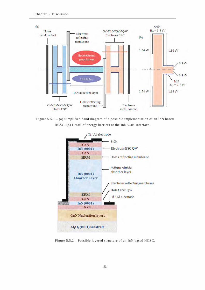
Chapter 5: Discussion
Figure 5.5.1 – (a) Simplified band diagram of a possible implementation of an InN based
HCSC. (b) Detail of energy barriers at the InN/GaN interface.
Figure 5.5.2 – Possible layered structure of an InN based HCSC.
151
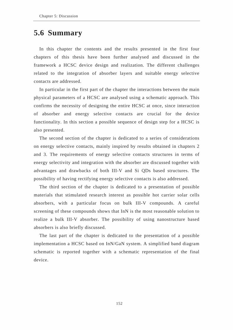
Chapter 5: Discussion
152
5.6 Summary
In this chapter the contents and the results presented in the first four
chapters of this thesis have been further analysed and discussed in the
framework a HCSC device design and realization. The different challenges
related to the integration of absorber layers and suitable energy selective
contacts are addressed.
In particular in the first part of the chapter the interactions between the main
physical parameters of a HCSC are analysed using a schematic approach. This
confirms the necessity of designing the entire HCSC at once, since interaction
of absorber and energy selective contacts are crucial for the device
functionality. In this section a possible sequence of design step for a HCSC is
also presented.
The second section of the chapter is dedicated to a series of considerations
on energy selective contacts, mainly inspired by results obtained in chapters 2
and 3. The requirements of energy selective contacts structures in terms of
energy selectivity and integration with the absorber are discussed together with
advantages and drawbacks of both III-V and Si QDs based structures. The
possibility of having rectifying energy selective contacts is also addressed.
The third section of the chapter is dedicated to a presentation of possible
materials that stimulated research interest as possible hot carrier solar cells
absorbers, with a particular focus on bulk III-V compounds. A careful
screening of these compounds shows that InN is the most reasonable solution to
realize a bulk III-V absorber. The possibility of using nanostructure based
absorbers is also briefly discussed.
The last part of the chapter is dedicated to the presentation of a possible
implementation a HCSC based on InN/GaN system. A simplified band diagram
schematic is reported together with a schematic representation of the final
device.

Chapter 5: Discussion
153
5.7 Bibliography
1. Aliberti, P., Y. Feng, Y. Takeda, S.K. Shrestha, M.A. Green, and G.J.
Conibeer, Investigation of theoretical efficiency limit of hot carrier
solar cells with bulk InN absorber. Journal of Applied Physics, 2010.
108(9): p. 094507-10.
2. Conibeer, G., R. Patterson, L. Huang, J.-F. Guillemoles, D. König, S.K.
Shrestha, and M.A. Green, Modelling of hot carrier solar cell absorbers.
Solar energy materials and solar cells, 2010. 94(9): p. 1516-1521.
3. Wurfel, P., The chemical potential of radiation. Journal of Physics C-
Solid State Physics, 1982. 15(18): p. 3967-3985.
4. Takeda, Y., T. Ito, T. Motohiro, D. König, S.K. Shrestha, and G.
Conibeer, Hot carrier solar cells operating under practical conditions.
Journal of Applied Physics, 2009. 105(7): p. 074905-10.
5. Aliberti, P., S.K. Shrestha, R. Teuscher, B. Zhang, M.A. Green, and G.J.
Conibeer, Study of silicon quantum dots in a SiO2 matrix for energy
selective contacts applications. Solar energy materials and solar cells,
2010. 94(11): p. 1936-1941.
6. Aliberti, P., B.P. Veettil, R. Li, S.K. Shrestha, B. Zhang, A. Hsieh, M.A.
Green, and G. Conibeeer, Investigation of single layers of silicon
quantum dots in SiO2 matrix for energy selective contacts in hot carriers
solar cells, in AuSES Conference. 2010: Canberra - Australia.
7. Berghoff, B., S. Suckow, R. Rolver, B. Spangenberg, H. Kurz, A.
Dimyati, and J. Mayer, Resonant and phonon-assisted tunneling
transport through silicon quantum dots embedded in SiO2. Applied
Physics Letters, 2008. 93(13): p. 132111.
8. Jiang, C.W., M.A. Green, E.C. Cho, and G. Conibeer, Resonant
tunneling through defects in an insulator: Modeling and solar cell
applications. Journal of Applied Physics, 2004. 96(9): p. 5006-5012.
9. Bayram, C., Z. Vashaei, and M. Razeghi, Reliability in room-
temperature negative differential resistance characteristics of low-
aluminum content AlGaN/GaN double-barrier resonant tunneling
diodes. Applied Physics Letters, 2010. 97(18): p. 181109-3.

Chapter 5: Discussion
154
10. Kikuchi, A., R. Bannai, K. Kishino, C.M. Lee, and J.I. Chyi, AlN/GaN
double-barrier resonant tunneling diodes grown by rf-plasma-assisted
molecular-beam epitaxy. Applied Physics Letters, 2002. 81(9): p. 1729-
1731.
11. Litvinov, V.I., Resonant Tunneling in III-Nitrides. Proceedings of the
Ieee, 2010. 98(7): p. 1249-1254.
12. Kikuchi, A., T. Yamada, S. Nakamura, K. Kusakabe, D. Sugihara, and
K. Kishino, Improvement of crystal quality of rf-plasma-assisted
molecular beam epitaxy grown Ga-polarity GaN by high-temperature
grown AlN multiple intermediate layers. Japanese Journal of Applied
Physics Part 2-Letters, 2000. 39(4B): p. L330-L333.
13. Briot, O., S. Ruffenach, M. Moret, B. Gil, C. Giesen, M. Heuken, S.
Rushworth, T. Leese, and M. Succi, Growth of InN films and
nanostructures by MOVPE. Journal of Crystal Growth, 2009. 311(10): p.
2761-2766.
14. Kadir, A., M.R. Gokhale, A. Bhattacharya, A. Pretorius, and A.
Rosenauer, MOVPE growth and characterization of InN/GaN single and
multi-quantum well structures. Journal of Crystal Growth, 2008. 311(1):
p. 95-98.
15. Yarar, Z., B. Ozdemir, and M. Ozdemir, Transport and Mobility
Properties of Bulk Indium Nitride (InN) and a Two-Dimensional
Electron Gas in an InGaN/GaN Quantum Well. Journal of Electronic
Materials, 2007. 36(10): p. 1303-1312.
16. Kim, J.W., K.H. Lee, and S. Hong, Structural and optical
characteristics of InN/GaN multiple quantum wells grown by
metalorganic chemical vapor deposition. Thin Solid Films, 2007.
515(10): p. 4405-4407.
17. Conibeer, G., N. Ekins-Daukes, J.-F. Guillemoles, D. König, E. Cho,
C.W. Jiang, S.K. Shrestha, and M.A. Green, Progress on hot carrier
cells. Solar energy materials and solar cells, 2009. 93(6-7): p. 713-719.
18. Deligoz, E., K. Colakoglu, Y.O. Ciftci, and H. Ozisik, The first
principles study on boron bismuth compound. Computational Materials
Science, 2007. 39(3): p. 533-540.

Chapter 5: Discussion
155
19. Rosenwaks, Y., M.C. Hanna, D.H. Levi, D.M. Szmyd, R.K. Ahrenkiel,
and A.J. Nozik, Hot carrier cooling in GaAs - quantum wells versus
bulk. Physical Review B, 1993. 48(19): p. 14675-14678.
20. Damen, T.C., J. Shah, D.Y. Oberli, D.S. Chemla, J.E. Cunningham, and
J.M. Kuo, Dynamics of exciton formation and relaxation in GaAs
quantum wells. Physical Review B, 1990. 42(12): p. 7434-7438.
21. Colvard, C., T.A. Gant, M.V. Klein, R. Merlin, R. Fischer, H. Morkoc,
and A.C. Gossard, Folded acoustic and quantized optic phonons in
(GaAl)As superlattices. Physical Review B, 1985. 31(4): p. 2080.
22. Daiminger, F., A. Schmidt, K. Pieger, F. Faller, and A. Forchel.
Thermalization and band renormalization in the zero-dimensional
electron-hole system in InGaAs / GaAs quantum dots. in 8th
International Conference on Hot Carriers in Semiconductors. 1993.
Oxford, England: Iop Publishing Ltd.
23. Syperek, M., P. Leszczynski, J. Misiewicz, E.M. Pavelescu, C. Gilfert,
and J.P. Reithmaier, Time-resolved photoluminescence spectroscopy of
an InGaAs/GaAs quantum well-quantum dots tunnel injection structure.
Applied Physics Letters. 96(1): p. 011901-3.
24. Xu, Z.C., Y.T. Zhang, and J.M. Hvam, Long luminescence lifetime in
self-assembled InGaAs/GaAs quantum dots at room temperature.
Applied Physics Letters, 2008. 93(18): p. 183116-3.
25. Bockelmann, U. and G. Bastard, Phonon scattering and energy
relaxation in two-, one-, and zero-dimensional electron gases. Physical
Review B, 1990. 42(14): p. 8947.
26. Kurtze, H., J. Seebeck, P. Gartner, D.R. Yakovlev, D. Reuter, A.D.
Wieck, M. Bayer, and F. Jahnke, Carrier relaxation dynamics in self-
assembled semiconductor quantum dots. Physical Review B, 2009.
80(23): p. 235319-7.
27. Kuntermann, V., C. Cimpean, G. Brehm, G. Sauer, C. Kryschi, and H.
Wiggers, Femtosecond transient absorption spectroscopy of silanized
silicon quantum dots. Physical Review B, 2008. 77(11): p. 115343-8.


Chapter 6
CONCLUSIONS
AND FUTURE WORK

Chapter 6: Conclusions and future work
156
In this thesis different aspects related to the designing and the realization of
a hot carrier solar cell converter have been investigated. This project
contributes to the research in “third generation photovoltaics” which has the
aim of engineering novel solar cell devices that can overcome the Shockley-
Queisser efficiency limit.
The work is divided in five main chapters.
The first chapter gives an overview of the current world energy consumption
and generation, focusing the attention on the role of renewable energies in the
near future energy market. In this chapter an introduction to photovoltaic
devices is given with details of different “generations” of solar cells. The status
of current research in third generation is depicted before introducing the
concept and operating principle of the hot carrier solar cell. The main
theoretical aspects related to the functionality of the hot carrier solar cell are
briefly described introducing the detailed discussion presented in the rest of the
thesis.
In the second chapter the calculation of real efficiency limits for a hot
carrier solar cell based on an indium nitride absorber is presented. A hybrid
model, which takes into account both particle balance and energy balance, has
been implemented. The model allows consideration of the influence of real AR
and II rates on cell performances, together with actual thermalisation losses.
The real InN dispersion relation has been reconstructed using actual effective
masses for different bands and non-parabolicity effects. A maximum efficiency
of 43.6 percent has been found for 1000 suns solar concentration. A close
relation between carrier thermalisation velocity and solar cell maximum
efficiency has also been found. In the last section of the chapter the influence
of non-ideal energy selective contacts on cell performances is discussed. It was
found that to maintain high efficiency (39.6 percent) the width of the contacts
has to be about 20 meV.
Chapter 6: Conclusions and future work
157
In chapter three theoretical and experimental aspects of all-silicon energy
selective contacts for hot carrier solar cells are investigated. Structures
consisting of a single layer of silicon quantum dots in a silicon dioxide matrix
have been realised using radio frequency magnetron co-sputtering and high
temperature annealing. Physical and optical properties of silicon rich oxide and
silicon dioxide layers have been studied in order to optimize the characteristics
of the single layer quantum dot structures. Photoluminescence and absorption
measurements confirmed that the morphology of the nanoparticles in the films
is related to the former silicon excess values. It was found that an atomic ratio
of silicon to Oxygen around 0.9 allows obtaining good size distribution and
density of the silicon quantum dots. It has also been demonstrated that the
average size of the quantum dots can be accurately controlled modifying the
thickness of the silicon rich oxide layers and that the position of the
photoluminescence peak is directly related to the diameter of the quantum dots.
In addition the evolution of the PL signal during the annealing process has been
studied. It was found that the crystallization of the silicon quantum dots occurs
during the very early stage of the annealing process. Further evolution of the
physical and optical properties of the samples is strictly related to an Ostwald
ripening process and partial oxidation of the quantum dots in the annealing
atmosphere. The optical properties of the structures after furnace forming gas
treatments confirmed that defects at Si-SiO2 interface have an active role in the
photoluminescence process. These defects can create non-radiative
recombination centres but they do not generate any additional radiative paths
for confined excitons. Since no significant energy peak shift was observed after
forming gas annealing, it was concluded that the main mechanism underlying
the luminescence of sputtered single silicon quantum dots in silicon dioxide is
optical quantum confinement.
In the fourth chapter time resolved photoluminescence experiments have
been performed on III-V bulk semiconductors in order to investigate the factors
that influence hot carrier cooling processes. The influence of the hot phonon
effect and intervalley electron scattering on the hot carrier cooling rates of bulk
gallium arsenide and indium phosphide have been studied. Under high carrier
Chapter 6: Conclusions and future work
158
concentrations, a longer hot carrier cooling transient was observed in indium
Phosphide compared to Gallium Arsenide when electron energy is not high
enough to access satellite valleys. This proved the influence of the hot phonon
effect on the carrier relaxation. It was also demonstrated that intervalley
scattering decreases the hot carrier cooling rate into the main valley. The
Fröhlich interaction appears to dominate intervalley scattering, resulting in
slowing of carrier cooling in GaAs by storing hot electrons in side valleys. The
second half of this chapter is dedicated to the investigation of hot carrier
cooling in bulk wurtzite indium nitride samples. Time resolved
photoluminescence experiments have demonstrated that carriers can be excited
above 2000 K in indium nitride using laser pulses of 35 J at 1.1 eV. The
carrier temperature decays towards the lattice temperature with a time constant
around 7 ps, which demonstrates the presence of a pronounced hot phonon
effect in indium nitride.
In chapter five a review and discussion of results presented in the other
chapters is presented within the framework of the design of a hot carrier solar
cell. The interactions between the main physical parameters of the cell are
analysed and discussed, confirming that the hot carrier solar cell has to be
designed as a whole device at once. In fact, the interaction of absorber and
energy selective contacts properties are crucial for the device functionality.
The requirements of energy selective contacts in terms of energy selectivity
and integration with the absorber are discussed in this chapter together with the
possibility of having rectifying contacts. The last section of the chapter is
dedicated to a screening of possible III-V compounds which can be used as
potential hot carrier solar cell absorbers and to the presentation of a possible
implementation a hot carrier solar cell device.
This thesis investigated some of the basic aspects related to the development
of a hot carrier solar cell. The aim of the work was to study solutions and
materials in order to achieve actual progress towards the fabrication of the
device. Results have been obtained for the calculation of maximum efficiencies
of hot carrier solar cells, for the realization of energy selective contacts and in

Chapter 6: Conclusions and future work
159
addition a potential structure for a hot carrier solar cell based on III-V
compounds has been presented. However, this thesis is still to be considered as
a preliminary step towards the realization of a hot carrier solar cell, since this
task still faces great scientific and technological challenges. Much room exists
for further investigation of nanostructured absorbers, both in III-V compounds
and group IV materials, in order to obtain slower hot carrier cooling
behaviours. The electrical properties of energy selective contacts based on III-
V quantum wells has to be studied in order to optimize extraction from
different absorbers. Additional investigation is also required to study carrier
transport mechanisms in both absorbers and energy selective contacts, with the
aim of clarifying whether it is possible to extract carriers very rapidly after
generation, in order to prevent thermalisation losses.
In conclusion this thesis presents recent progresses towards the development
of the hot carrier solar cell. Results provide a detailed picture of this device in
terms of potential achievable efficiencies, development of absorber materials
and energy selective contacts. Findings of this work have to be considered as a
preliminary insight for the development of the hot carrier solar cell. Further
research is needed in order to accomplish the successful realization of an actual
device.