how low can we go - tau · pdf filehow how low can we low can we low ... near-threshold...
TRANSCRIPT
TAU 2016 PanelTAU 2016 PanelTAU 2016 PanelTAU 2016 Panel
How How How How Low Can We Low Can We Low Can We Low Can We GoGoGoGoChallenges when designing at ultra-low voltage
Moderator: Florin Dartu (TSMC)

Sriram. R. Vangal
• Dr. Sriram. R. Vangal received the Ph.D. degree in Electrical Engineering from Linköping University, Sweden. He joined Intel Corporation 20 years ago and is currently a Principal Research Scientist with Circuit Research Labs, Hillsboro, Oregon, USA.
• Sriram has played a lead role in multi-core CPU development and ultra-low power silicon research. He leads a research team in the areas of low-power high-performance circuits; energy-efficient near-threshold computing, network-on-chip (NoC) based multi-processing and fine-grained power management techniques. Sriram has published over 25 journal and conference papers including two book chapters on on-die interconnects, and has over 30 design patents in these areas. Sriram serves on VLSI design and NoC Symposium technical conference committees.
Kelvin Le
• Kelvin Le is currently a Principal Engineer at Synopsys, Mountain View, CA. Before joining Synopsys, he was a co-founder and principal scientist at Extreme-DA. Santa Clara. Kelvin Le received the Ph.D. degree in electrical and computer engineering from Carnegie Mellon University, Pittsburgh, PA, in 2006, and MS degree from Shanghai Jiao Tong University, China in 2001. His current research interests include statistical modeling, timing/power analysis and optimization.
Paul Penezes
• Paul Penzes is a Senior Director of Engineering at Qualcomm. As the lead of the Design Technology (DTECH) team, he manages the timing, PPA R&D, testchip and design technology integration teams within the Central Engineering and Technology organization. Before Qualcomm, Paul was an Associate Technical Director and Distinguished Engineer at Broadcom, and prior to that a Senior VLSI Engineer and Myricom. Paul has 19 patents issued, 14 pending, and has a B.S., an M.S. and a Ph.D in Computer Science from the California Institute of Technology, Pasadena.
Christian Lutkemeyer
• Christian Lutkemeyer is a Senior Technical Director at ClariPhy Inc., a leading provider of 100G to 400G and beyond optical coherent transport solutions. The work described in the presentation was done while he was a Technical Director in the Office of the CTO of Broadcom Corp. (now Ltd.), where he lead the Nanometer-Signoff Center-of-Excellence, until joining ClariPhy in February 2016.

Satheesh Balasubramanian
• Satheesh Balasubramanian holds a B.Tech degree in Metallurgical Engineering from the Indian Institute of Technology Madras and a MS from Penn State University. He was in the Library Design Group in Texas Instruments for about 10 years. He is currently with ARM. His interests are in all aspects of library design and how it impacts the end SoC.
RELIABLE LOW-VOLTAGE
COMPUTING
Sriram Vangal, Intel Labs
Acknowledgements: many individuals a/c Intel Labs and Intel

Wide Dynamic Range 280mV/3MHz/2mW to 1.2V/915MHz/737mW
Minimum-energy
Design:
Pentium-class IA
processor (prototype)
Log Scale
S. Jain (et. al), A 280mV-to-1.2V wide-operating-range IA-32
processor in 32nm CMOS, ISSCC 2012S. Paul (et. al), A 3.6GB/s 1.3mW 400mV 0.051mm
Near-Threshold Voltage Resilient Router in 22nm Tri-gate CMOS, 2013 VLSI Circuits Symposium
8
Note memory VDD ≥ Logic rail

Key Challenges for NTV Operation
Need architecture and circuit solutions to mitigate effects of NTV
Increased delay
variability- need
SSTA flows
NTV
OperationMemory read/
write/retention
failures
Low static noise
margins
Flops setup/
hold delay
degradation
Failures in
contention
circuits
Performance
degradation
9
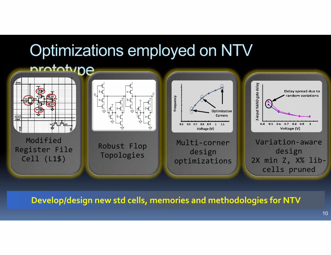
Optimizations employed on NTV
prototype
Modified Register File Cell (L1$)
Robust Flop Topologies
Develop/design new std cells, memories and methodologies for NTV
Multi-corner design
optimizations
Fre
qu
en
cyF
req
ue
ncy
Variation-aware design
2X min Z, X% lib-cells pruned
10

Reliable computing using unreliable
components� Architecture & Circuit solutions
� Partition DVFS islands optimally for best energy-efficiency (@ cost of VR overheads)
� Datapath: double-sampling sequentials (aka Razor), tunable critical path replica circuits
� Combined NTV + resiliency techniques, recovery via instruction replay (S. Paul et. al, VLSI 2013) � Learnings: you do guard-band more at NTV, but opportunity to recover excess guard-band is also better
� Need of the Hour:
o Low-overhead NTV circuits, ULV standard cell libraries (both logic and memory)
o Methodologies for Low Vcc & WDR designs : SSTA, Multipoint optimizationo Scalable hold-buffer insertion methodology (huge issue!)
o Lowering retention voltages (VMIN) in memories & sequentials
o Must be combined with adaptive resilient computing for maximum benefit/robustness
o Device – Circuits – Architecture co-design for reliable low-voltage operation
11

ClariPhy Confidential
How low can we go? Challenges when
designing at ultra-low voltage
Christian Lütkemeyer
March 11, 2016

ClariPhy Confidential
3/11/2016
Sources of Timing Variation in Digital Circuits
14
Process Voltage Temperature
InterconnectLocal Variation
Coupling (SI) Aging
Spatial Variation
Simultaneous Switching

MOS-FET Current and Gate Delay
15© ClariPhy 3/11/2016
VGS
log(Isubth)
VT
D
G
S
Isubth
Subthreshold Slope
[~ 70mV /decade]
log(gate delay)
VTHVTL
VDD
LVT
HVT

Timing Trends at Low Supply Voltages
• Gate delays and their variations become more important than interconnect delays.
– Simplified interconnect modeling is ok.
• Gate delay variation becomes significantly skewed 1).
– Mean timing optimism at the global corner.
• Stronger dependence of delay on the input waveform shape.
– The tail matters!
– STA accuracy challenge.
– Small supply changes create large delay changes.
3/20/2016 16ClariPhy Confidential
1) P. Ghanta, I. Keller: “Importance of Modeling Non-Gaussianities in Static Timing Analysis
in sub-16nm Technologies,” Tau 2016
Design Guidelines
• Create a solid foundation: Eliminate, optimize, or replace marginal circuits.
– 6T memory bit cells, level shifters, pass gates, etc.
• Build well: Use robust design principles.
– Low variation clock trees (use large LVT inverters, minimize length of non-common clock paths).
– Instead of matching use matching plus margin.
– HVT hold fixing cells. Insert half cycle delays as needed.
– Use worst case replica circuits for AVS with sufficient margin. Consider especially spatial variation, i.e. intra die performance gradients.
– Scale “constant” margins with supply voltage.
• 50ps at 0.8V may have to become 500ps at 0.5V.
3/20/2016 17ClariPhy Confidential
Understand your Overall Design Margins
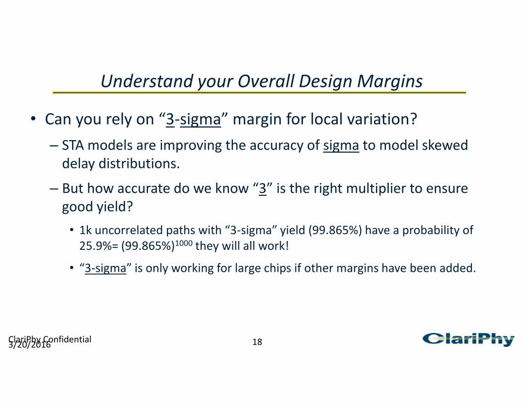
• Can you rely on “3-sigma” margin for local variation?
– STA models are improving the accuracy of sigma to model skewed
delay distributions.
– But how accurate do we know “3” is the right multiplier to ensure
good yield?
• 1k uncorrelated paths with “3-sigma” yield (99.865%) have a probability of
25.9%= (99.865%)1000 they will all work!
• “3-sigma” is only working for large chips if other margins have been added.
3/20/2016 18ClariPhy Confidential
The saving grace: Large setup timing violations in silicon can
be fixed with small increases of supply voltage if basic cells
do not fail, and robust design principles are followed.
Thank You!
19ClariPhy Confidential

Kelvin Le
03/11/2016
Challenges at ultra low voltages

© 2016 Synopsys, Inc. 21
Signoff Challenges at Low Power FinFET
• Near-threshold operations at FinFET
technology exhibit new timing
challenges
– Waveform distortion effect
– Larger and asymmetric variation
– Wider operating voltage challenges
• Waveform-centric calculation
methodology can be used to address
nominal accuracy
– Impact library characterization and
qualification
• Large timing variation impacts both
design methodology and analysis
Low Power Technology Node
VDD
Po
wer
(log
)
Vth
Total
Dynamic
Leakage
Vop
Waveform Impact Variation Impact
Longer tail Asymmetric & larger σ
Advanced
propagation
Advanced
waveform
propagation
POCV LVF
© 2016 Synopsys, Inc. 22
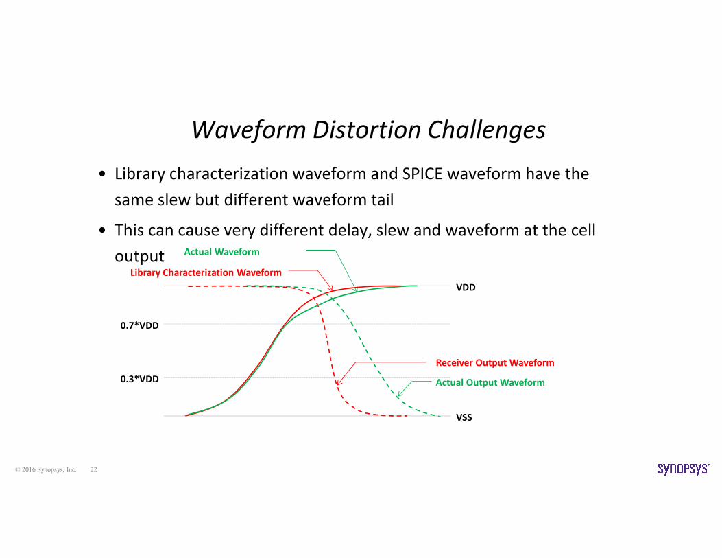
• Library characterization waveform and SPICE waveform have the
same slew but different waveform tail
• This can cause very different delay, slew and waveform at the cell
output
Waveform Distortion Challenges
Actual Output Waveform
VDD
VSS
0.7*VDD
0.3*VDD
Library Characterization Waveform
Receiver Output Waveform
Actual Waveform
© 2016 Synopsys, Inc. 23
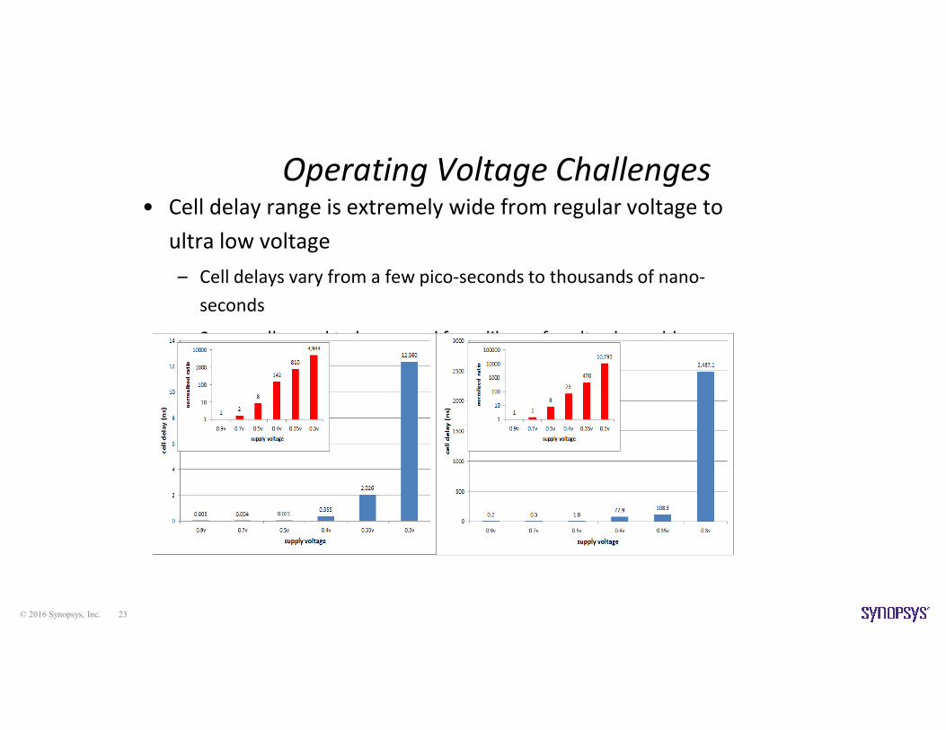
• Cell delay range is extremely wide from regular voltage to
ultra low voltage
– Cell delays vary from a few pico-seconds to thousands of nano-
seconds
– Some cells need to be pruned from library for ultra-low vdd
operations
– Expect challenges in hold and DRC fixing
Operating Voltage Challenges
© 2016 Synopsys, Inc. 24
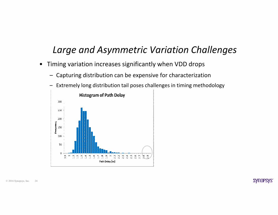
Large and Asymmetric Variation Challenges
• Timing variation increases significantly when VDD drops
– Capturing distribution can be expensive for characterization
– Extremely long distribution tail poses challenges in timing methodology

© 2016 Synopsys, Inc. 25
Large and Asymmetric Variation Challenges
• Timing variation increases significantly when VDD drops
– The variation magnitude is comparable with nominal value
– The distribution of variation also demonstrates strong bias
1
4
70
20
40
60
80
1 2 3 4 5 6 7 8 910
Sigma/Nominal of delay distribution (%)
1
4
7
0
0.5
1
1.5
2
2.5
1 2 3 4 5 6 7 8 9 10
Skewness of delay distribution

CONFIDENTIAL26
How Low Can We Go?
Satheesh BalasubramanianARM
11th March 2016
CONFIDENTIAL27
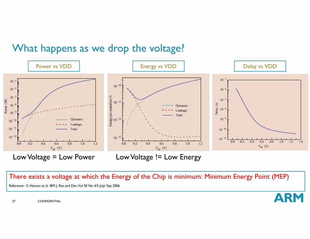
Low Voltage = Low Power
What happens as we drop the voltage?
Power vs VDD Energy vs VDD Delay vs VDD
There exists a voltage at which the Energy of the Chip is minimum: Minimum Energy Point (MEP)Reference– S. Hanson et al. IBM J. Res and Dev Vol 50 No 4/5 July/ Sep 2006
Low Voltage != Low Energy
CONFIDENTIAL28
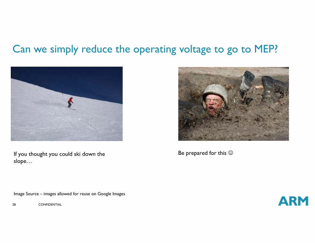
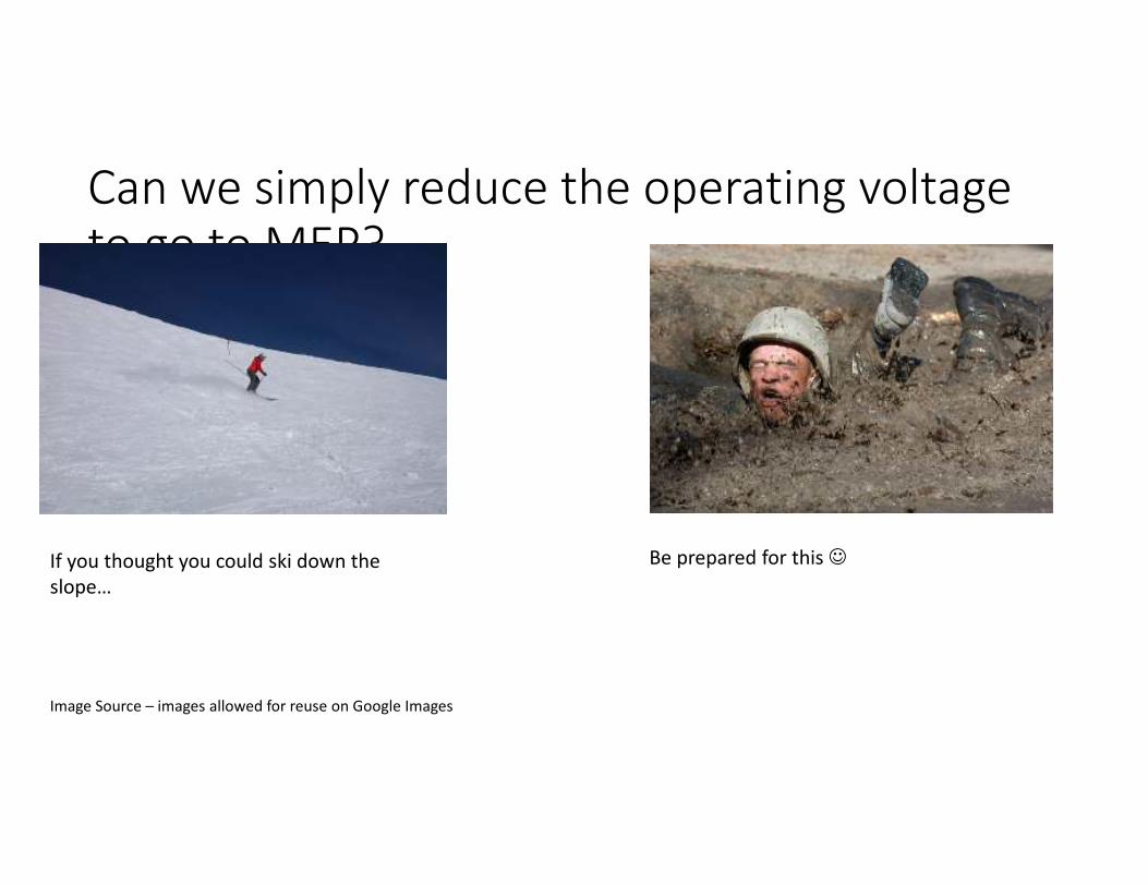
Can we simply reduce the operating voltage to go to MEP?
If you thought you could ski down the slope…
Be prepared for this ☺
Image Source – images allowed for reuse on Google Images
CONFIDENTIAL29
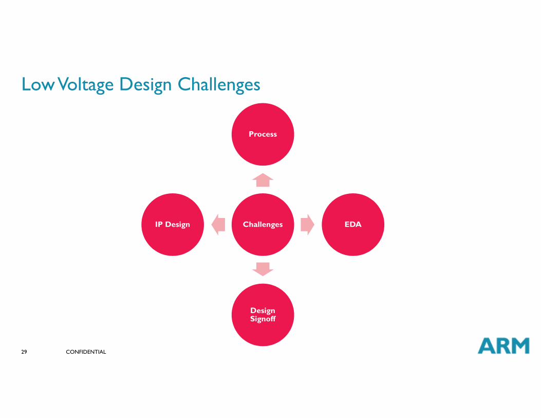
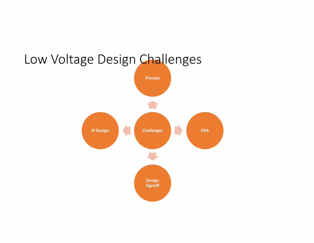
Challenges
Process
EDA
Design Signoff
IP Design
Low Voltage Design Challenges
CONFIDENTIAL30
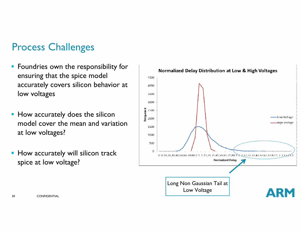
� Foundries own the responsibility for ensuring that the spice model accurately covers silicon behavior at low voltages
� How accurately does the silicon model cover the mean and variation at low voltages?
� How accurately will silicon track spice at low voltage?
Process Challenges
Long Non Gaussian Tail at Low Voltage

CONFIDENTIAL31
Library/ IP Challenges
� IP Vendors are responsible for ensuring the robustness of library at low voltages
� Verifying functional behavior at low voltages
� Ensuring accurate modelling of delay and variation at low voltages
� Highlighting cells with large variation to the SoC groups

CONFIDENTIAL32
� Dealing with Non-Gaussian behavior of Spice models
� Industry-wide shift to Liberty Variance Format (LVF) from AOCV format
� Dealing with Process and Voltage Variation
� Agreeing on a standard for modelling non-Gaussian behavior and voltage variation in LVF
EDA Vendor Challenges

CONFIDENTIAL33
� Finding the right voltage of operation for their design
� Dealing with memories since they can’t operate at ultra low voltages
� Designing a reliable voltage regulator that works at low voltages
� Dealing with cells that have large variations
� Determining if scan testing is required at low voltages
SoCTeam Responsibilities and Challenges
CONFIDENTIAL34
� There is definite value in operating at (the right!) low voltages
� Foundries, IP vendors, EDA Vendors and SoC companies all have crucial responsibilities to fulfill to make low voltage design a success
� Close collaboration between these four entities will make the low voltage design ecosystem successful
Summary

How Low Can We Go?Satheesh Balasubramanian
ARM
11th March 2016

Low Voltage = Low Power
What happens as we drop the voltage?Power vs VDD Energy vs VDD Delay vs VDD
There exists a voltage at which the Energy of the Chip is minimum: Minimum Energy Point (MEP)
Reference– S. Hanson et al. IBM J. Res and Dev Vol 50 No 4/5 July/ Sep 2006
Low Voltage != Low Energy
Can we simply reduce the operating voltage to go to MEP?
If you thought you could ski down the
slope…
Be prepared for this ☺
Image Source – images allowed for reuse on Google Images
Challenges
Process
EDA
Design
Signoff
IP Design
Low Voltage Design Challenges

• Foundries own the responsibility for ensuring that the spice model accurately covers silicon behavior at low voltages
• How accurately does the silicon model cover the mean and variation at low voltages?
• How accurately will silicon track spice at low voltage?
Process Challenges
Long Non Gaussian Tail at
Low Voltage

Library/ IP Challenges• IP Vendors are responsible for
ensuring the robustness of library at low voltages
• Verifying functional behavior at low voltages
• Ensuring accurate modelling of delay and variation at low voltages
• Highlighting cells with large variation to the SoC groups

• Dealing with Non-Gaussian behavior of Spice models
• Industry-wide shift to Liberty Variance Format (LVF) from AOCV format
• Dealing with Process and Voltage Variation
• Agreeing on a standard for modelling non-Gaussian behavior and voltage variation in LVF
EDA Vendor Challenges

• Finding the right voltage of operation for their design
• Dealing with memories since they can’t operate at ultra low voltages
• Designing a reliable voltage regulator that works at low voltages
• Dealing with cells that have large variations
• Determining if scan testing is required at low voltages
SoC Team Responsibilities and Challenges
• There is definite value in operating at (the right!) low voltages
• Foundries, IP vendors, EDA Vendors and SoC companies all have crucial responsibilities to fulfill to make low voltage design a success
• Close collaboration between these four entities will make the low voltage design ecosystem successful
Summary
Confidential
Igor Keller
TAU
Sonoma, CA
March 11th, 2016
Challenges at Low Voltages

45 © 2015 Cadence Design Systems, Inc. Cadence confidential. Internal use only.
• Why low power?– Mobile applications
– Internet of things
– Overheating at low geometries
– To bring oil prices down
• How to reduce power– Power/clock gating
– Reduced Voltage
– Higher Vt
– F.
Saving Private Power
power

46 © 2015 Cadence Design Systems, Inc. Cadence confidential. Internal use only.
• Underlying physics is simple• Vdd scales faster than Vt
• I ~= K/(Vdd – Vt)
• Challenges• Waveform (tail) effects
• IR drop on timing
• SI delay
• Voltage scaling
• More skewness in SOCV
• Relief• Glitch
• Slower clocks => larger denominator
Key Challenges with Low Voltage
Vdd=0.5V
Vt=0.3V
Vdd=1V
0.2V
0.6V
47 © 2015 Cadence Design Systems, Inc. Cadence confidential. Internal use only.
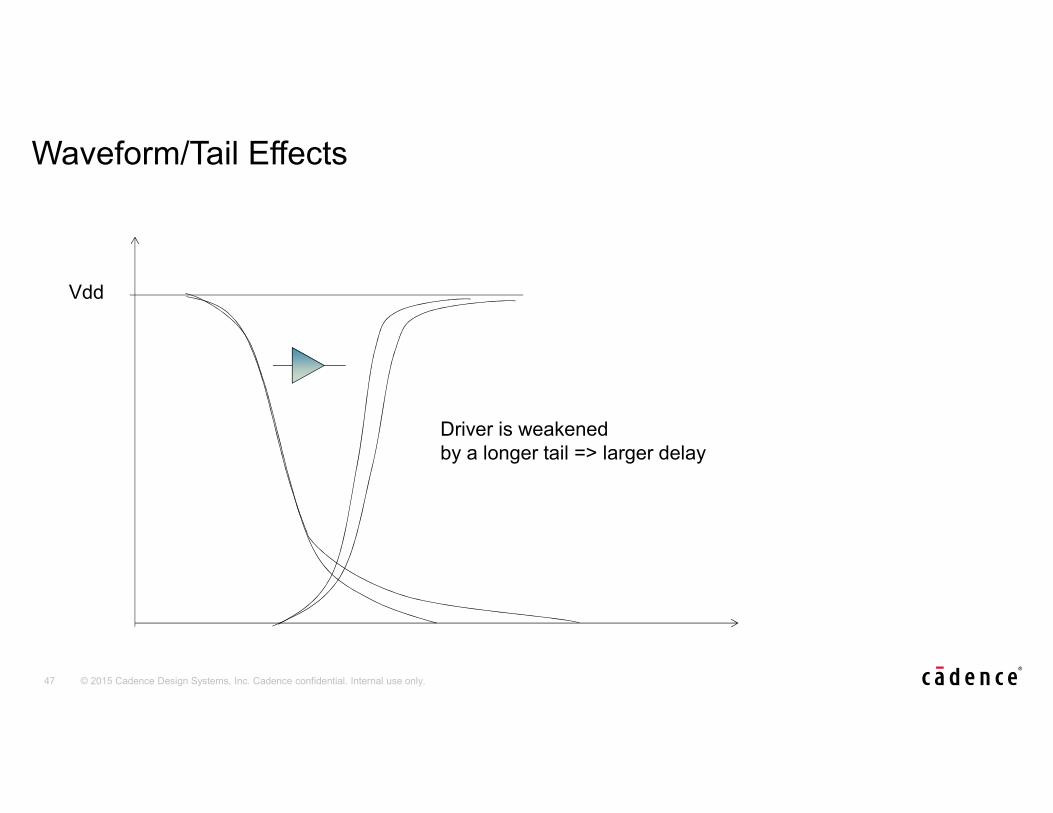
Waveform/Tail Effects
Vdd
Driver is weakened
by a longer tail => larger delay
48 © 2015 Cadence Design Systems, Inc. Cadence confidential. Internal use only.
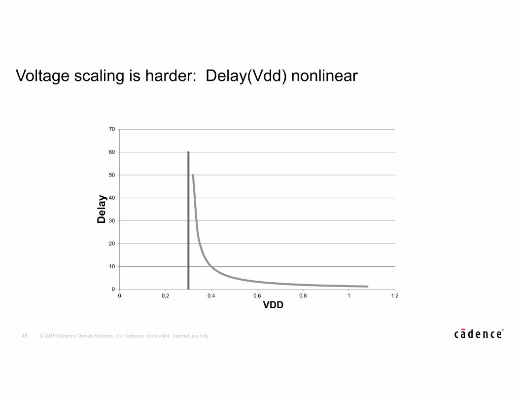
Voltage scaling is harder: Delay(Vdd) nonlinear
0
10
20
30
40
50
60
70
0 0.2 0.4 0.6 0.8 1 1.2
Delay
VDD
49 © 2015 Cadence Design Systems, Inc. Cadence confidential. Internal use only.
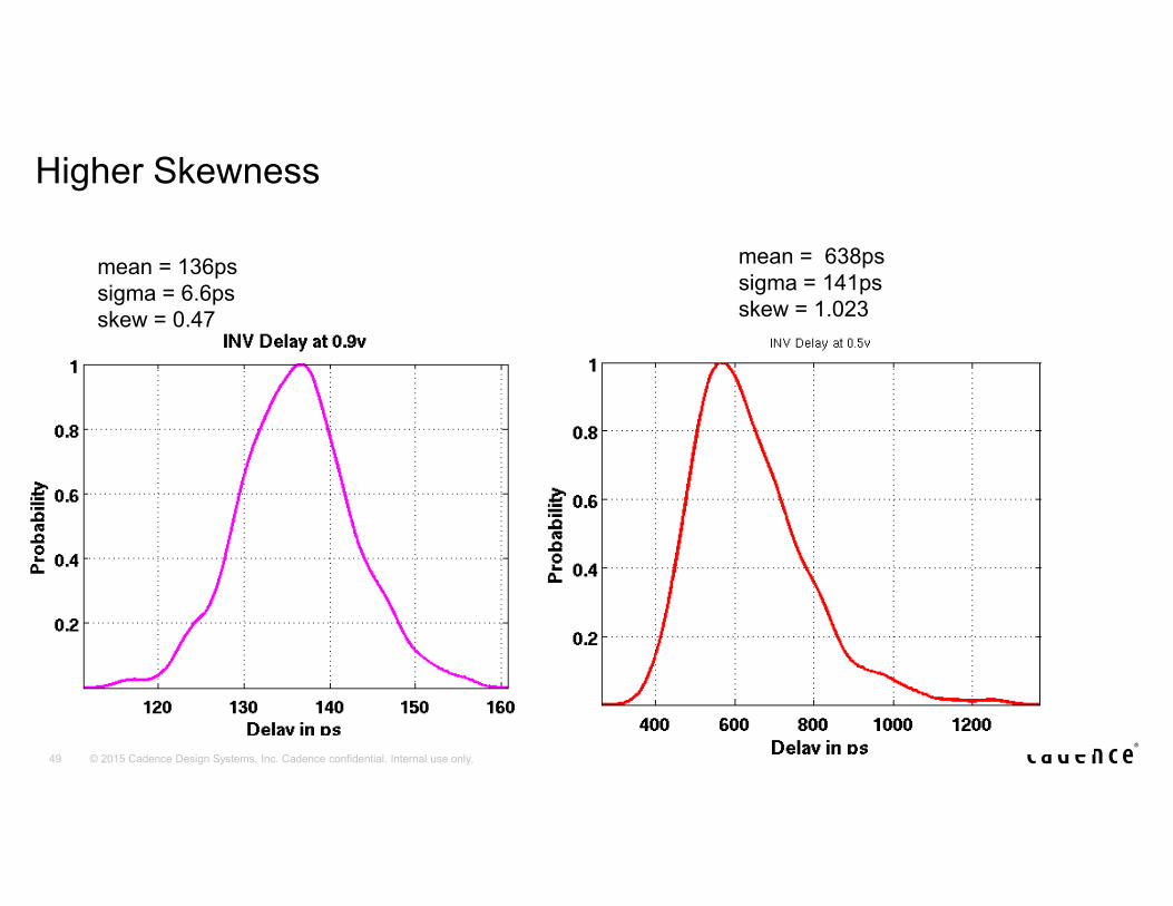
Higher Skewness
mean = 638ps
sigma = 141ps
skew = 1.023
mean = 136ps
sigma = 6.6ps
skew = 0.47
50 © 2015 Cadence Design Systems, Inc. Cadence confidential. Internal use only.
• Better gate model– More information about the tail
– More physical input waveform
– Finer slew indices
– More caps below slew threshold – Available in ECSM
– Maybe new model, independent on WF completely
• More information about variability– Capture PDF shape more accurately, 3 or more moments
• Better IR-drop analysis– Accurate V(t) prediction accounting for I(V)
– Tighter integration with STA
• More Libraries at finer Vdd step– Or better voltage scaling techniques
Future Improvements in STA at Low VDD