how secure are printed circuit boards against trojan...
TRANSCRIPT
2168-2356 (c) 2013 IEEE. Personal use is permitted, but republication/redistribution requires IEEE permission. Seehttp://www.ieee.org/publications_standards/publications/rights/index.html for more information.
This article has been accepted for publication in a future issue of this journal, but has not been fully edited. Content may change prior to final publication. Citation information: DOI10.1109/MDAT.2014.2347918, IEEE Design and Test
How Secure Are Printed Circuit Boards Against Trojan Attacks?
Swaroop GhoshDept. of CSE
University of S. FloridaTampa, FL 33620, [email protected]
Abhishek BasakDept. of EECS
Case Western Reserve U.Cleveland, OH 44106, USA
Swarup BhuniaDept. of EECS
Case Western Reserve U.Cleveland, OH 44106, USA
Abstract— Malicious modification of a design in a foundryor design house, referred to as hardware Trojan attacks, areintended to act as a spy or terrorist-on-chip. While these attackshave emerged as major security concerns for Integrated Circuits(ICs), in this paper, we demonstrate similar vulnerabilities athigher level, in particular for Printed Circuit Boards (PCBs).We note that increasing complexity of modern PCBs andgrowing reliance on third party entities make Trojan attacksin PCBs highly feasible. We introduce possible attack modelsand demonstrate instances for hardware Trojan insertion infabricated PCBs that can either cause malfunction or leak secretinformation. Our investigation reveals that traditional PCBtest methodologies can often be ineffective in detecting theseTrojans. We also explore possible protection approaches againstsuch attacks including a Reverse Engineering-based detectionapproach and a low-overhead preventive design solution.
Index Terms— Printed Circuit Board, PCB Trojan, Reverse-engineering
I. INTRODUCTION
Hardware Trojan attacks at the integrated circuit (IC)level have been studied extensively in recent times [1].Researchers have analyzed the impact of these attacks andexplored possible countermeasures for ICs [9] [10]. However,vulnerability with respect to hardware Trojan attacks athigher levels of system abstraction, e.g. at Printed CircuitBoard (PCB) level, have not been reported earlier. Previousstudies have covered security of PCBs against piracy andvarious post-fabrication tampering attacks. JTAG (Joint TestAccess Group) and other field programmability features e.g.,probe pins, unused sockets and USB have been extensivelyexploited by hackers to gain access to internal features ofthe designs [2] as well as snooping of secret key, collectionof test responses, and manipulating JTAG test pins [3]. Oneinstance demonstrated that Xbox can be hacked by disablingthe Digital Rights Management (DRM) policy using JTAG[4]. We note that modern PCBs are becoming increasinglyvulnerable to malicious modification of PCBs during designor fabrication in untrusted design or fabrication facilitiesunlike the widely reported in-field tampering attacks [2-4],such a vulnerability creates a new class of threat for PCBs.
The emerging business model of PCB design and fab-rication that favors extensive outsourcing and integrationof untrusted components/entities in the PCB life-cycle tolower manufacturing cost [5], makes hardware Trojan attacksin PCBs highly feasible. A closer look at several majorelectronic products and their PCB manufacturers reveals that
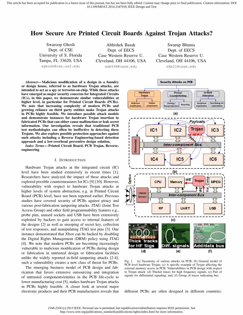
Fig. 1. (a) Taxonomy of various attacks on PCB; (b) General model ofPCB level hardware Trojan; (c) A specific example of Trojan affecting theexternal memory access in PCB. Vulnerabilities in PCB design with respectto Trojan attack: (d) Thicker traces for high frequency signals; (e) Pair ofsignals for differential signaling; and, (f) Group of traces indicating bus.
different PCBs are often designed in different countries.

2168-2356 (c) 2013 IEEE. Personal use is permitted, but republication/redistribution requires IEEE permission. Seehttp://www.ieee.org/publications_standards/publications/rights/index.html for more information.
This article has been accepted for publication in a future issue of this journal, but has not been fully edited. Content may change prior to final publication. Citation information: DOI10.1109/MDAT.2014.2347918, IEEE Design and Test
Moreover, reliance to third party manufacturing facilities,make the PCB fabrication process untrustworthy and hence,vulnerable to malicious modifications i.e. Trojan insertion.Furthermore, an adversary can be present inside the designhouse and the PCB design can be tampered with Trojans.Fig. 1(a) shows broad classes of attacks on PCB includingpossible Trojan attacks. In this paper, for the first time to ourknowledge, we analyze the feasibility of such attack; presentattack models and instances of hard-to-detect Trojans; andpropose possible countermeasures.
PCBs in today’s complex and highly integrated designscontain as many as 20-30 layers with hidden vias andembedded passive components [12] to minimize the PCBform factor. This presents great opportunity for an attackerto deliberately modify the PCB design by tampering theinterconnect lines at the internal layers or altering the com-ponents. Fig. 1(b) shows a general model of PCB hardwareTrojan. Fig. 1(c) illustrates an example where the externalmemory content is modified by tampering the write enablesignal. Similar to its IC counterpart, a PCB Trojan can servetwo purposes for an adversary: (1) cause malfunction; or (2)leak secret information. For example, an added capacitor ona signal line can significantly slowdown the communicationbetween the components in specific rare scenarios, makingthe product fail in field. Similarly, a hacker can access thesecret contents inside the components and alter/corrupt them.
II. THREAT ANALYSIS AND ATTACK MODELS
A. Security Analysis
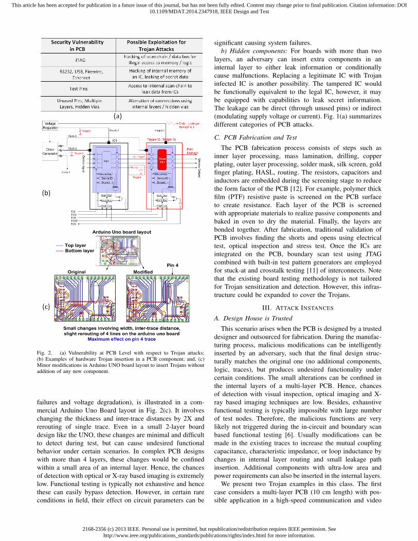
An attacker can exploit the vulnerabilities, design/testfeatures and test hooks that are available on the board. Somecommon PCB features that can be exploited by an adversaryfor understanding a design intent and efficiently mountinga Trojan attack with minimal design modification are asfollows.
1) JTAG interface: JTAG is an industry standard to enableboard level test and debug. It can be exploited by a hackerto get a clue about the hidden test features or hidden controlto access the data and address bus within the chip. Forexample, hackers can deduce information about the lengthand properties of the instruction register through JTAG bytrial and error. Next, a particular instruction can be executedto gain permission to tamper/feed internal data bus. JTAGcan also be used to Reverse Engineer (RE) the board de-sign by deducing the connectivity between components andexecuting external connectivity instructions.
2) Test pins or probe pads: Typical ICs contain severalprobe pads and test pins to observe/control important signalsfor test/debug purposes. A hacker can tap these pins andmonitor the interesting signals to gain critical informationabout the functionality of the design or feed malicious datainto the design. Test pins can also be used for RE where atest input can trigger certain data, address and control signalsthat can help identify the board functionality.
3) Vulnerabilities in PCB design: Fig. 1(d)-1(f) illustrateseveral additional vulnerabilities as described below.
a) Distinct properties of special signals: The thicknessof clock and data bus provides clues to the hackers aboutthe functionalities of these pins. Similarly, pins tied withidentical pull-up/down resistors indicate that they belong toa bus.
b) Remnant signatures from test/debug: When pins (thatare used for test/debug) are accessed through ports, theremnant of soldering provides clue to a hacker about thefunctionality of these pins. Similarly, an empty socket canbe used for hacking purposes.
c) Miscellaneous hints: Fig. 2(a) lists some additionalvulnerabilities. Apart from above component level hooks,a PCB design itself provides lots of information to anadversary in fabrication house that can facilitate powerfulTrojan attacks.
B. Attack Models
Trojan attacks in PCB can be divided into two broadclasses, as described below.
1) Case I: The board design is trusted: In this model,the attack is mounted in the PCB fabrication house. It isexpected that the attacker would change the design in a waythat evades post-manufacturing test, but causes functionaldeviations under certain rare conditions, which are unlikelyto be triggered during test.
2) Case II: The board design is not trusted (e.g. out-sourced): In this model, the attacker is assumed to be presentin the board design or fabrication house. Only the functionaland parametric specifications of the board are trusted. Theattacker has higher flexibility of maliciously altering thedesign and/or choosing fake or untrustworthy (and potentiallymalicious) components. Again, an attacker would try to hidethe modifications to avoid detection during functional andparametric testing process.
Note that in both cases, there are two possible objectives ofthe attacker: 1) malfunction, and/or 2) information leakage.Next, we describe possible Trojan attacks of different formsin a PCB.
a) Signal trace modifications in the inner PCB layers: Forboards with fewer levels where hiding an extra component isdifficult, an attacker can change the resistance, capacitanceor inductance of the signal traces (self, mutual). For example,signal trace in an internal layer can be made thinner toincrease the resistance such that it fails during long hourof operation due to heating. Similarly the metal coupling ca-pacitance, between two traces including traces in the supplyplanes can be increased (by changing trace dimensions, inter-trace distance via slight rerouting and selective dielectricproperty modification) to trigger coupling induced voltageand delay failures in one of the lines. Leakage resistancepaths can also be incorporated in an internal layer tracefor intentional voltage degradation. Impedance mismatchbetween interconnected traces can be introduced to causemalfunction in certain scenarios.
Modification in an example 4-trace scenario, causing ma-licious effects on circuit parameters (coupled voltage, delay
2168-2356 (c) 2013 IEEE. Personal use is permitted, but republication/redistribution requires IEEE permission. Seehttp://www.ieee.org/publications_standards/publications/rights/index.html for more information.
This article has been accepted for publication in a future issue of this journal, but has not been fully edited. Content may change prior to final publication. Citation information: DOI10.1109/MDAT.2014.2347918, IEEE Design and Test
Fig. 2. (a) Vulnerability at PCB Level with respect to Trojan attacks;(b) Examples of hardware Trojan insertion in a PCB component; and, (c)Minor modifications in Arduino UNO board layout to insert Trojans withoutaddition of any new component.
failures and voltage degradation), is illustrated in a com-mercial Arduino Uno Board layout in Fig. 2(c). It involveschanging the thickness and inter-trace distances by 2X andrerouting of single trace. Even in a small 2-layer boarddesign like the UNO, these changes are minimal and difficultto detect during test, but can cause undesired functionalbehavior under certain scenarios. In complex PCB designswith more than 4 layers, these changes would be confinedwithin a small area of an internal layer. Hence, the chancesof detection with optical or X-ray based imaging is extremelylow. Functional testing is typically not exhaustive and hencethese can easily bypass detection. However, in certain rareconditions in field, their effect on circuit parameters can be
significant causing system failures.b) Hidden components: For boards with more than two
layers, an adversary can insert extra components in aninternal layer to either leak information or conditionallycause malfunctions. Replacing a legitimate IC with Trojaninfected IC is another possibility. The tampered IC wouldbe functionally equivalent to the legal IC, however, it maybe equipped with capabilities to leak secret information.The leakage can be direct (through unused pins) or indirect(modulating supply voltage or current). Fig. 1(a) summarizesdifferent categories of PCB attacks.
C. PCB Fabrication and Test
The PCB fabrication process consists of steps such asinner layer processing, mass lamination, drilling, copperplating, outer layer processing, solder mask, silk screen, goldfinger plating, HASL, routing. The resistors, capacitors andinductors are embedded during the screening stage to reducethe form factor of the PCB [12]. For example, polymer thickfilm (PTF) resistive paste is screened on the PCB surfaceto create resistance. Each layer of the PCB is screenedwith appropriate materials to realize passive components andbaked in oven to dry the material. Finally, the layers arebonded together. After fabrication, traditional validation ofPCB involves finding the shorts and opens using electricaltest, optical inspection and stress test. Once the ICs areintegrated on the PCB, boundary scan test using JTAGcombined with built-in test pattern generators are employedfor stuck-at and crosstalk testing [11] of interconnects. Notethat the existing board testing methodology is not tailoredfor Trojan sensitization and detection. However, this infras-tructure could be expanded to cover the Trojans.
III. ATTACK INSTANCES
A. Design House is Trusted
This scenario arises when the PCB is designed by a trusteddesigner and outsourced for fabrication. During the manufac-turing process, malicious modifications can be intelligentlyinserted by an adversary, such that the final design struc-turally matches the original one (no additional components,logic, traces), but produces undesired functionality undercertain conditions. The small alterations can be confined inthe internal layers of a multi-layer PCB. Hence, chancesof detection with visual inspection, optical imaging and X-ray based imaging techniques are low. Besides, exhaustivefunctional testing is typically impossible with large numberof test nodes. Therefore, the malicious functions are verylikely not triggered during the in-circuit and boundary scanbased functional testing [6]. Usually modifications can bemade in the existing traces to increase the mutual couplingcapacitance, characteristic impedance, or loop inductance bychanges in internal layer routing and small leakage pathinsertion. Additional components with ultra-low area andpower requirements can also be inserted in the internal layers.
We present two Trojan examples in this class. The firstcase considers a multi-layer PCB (10 cm length) with pos-sible application in a high-speed communication and video

2168-2356 (c) 2013 IEEE. Personal use is permitted, but republication/redistribution requires IEEE permission. Seehttp://www.ieee.org/publications_standards/publications/rights/index.html for more information.
This article has been accepted for publication in a future issue of this journal, but has not been fully edited. Content may change prior to final publication. Citation information: DOI10.1109/MDAT.2014.2347918, IEEE Design and Test
Fig. 3. Impact of Trojans in a PCB inserted by selective trace/s property modification, without addition of any new component (design house trustedscenario): (a) Lumped 2 trace PCB model with associated capacitance, inductance and resistance; (b) Trace-2 near and far end voltages and (c) Propagationdelay in trace-1 (n1 and n4 nodes) at 220MHz, 3V p-p input; (d) Effect on trace-1 far end voltage, on insertion of a leakage resistance path from trace-1to ground; (e) and (f) show the effect of change in trace properties in a 4-wire scenario; Coupled voltages in near and far end of victim trace when allaggressors are switching in phase at 220 MHz and 3V peak-to-peak (p-p), is illustrated in (e) and voltage profile at near end (n9) of trace 3 and far end(n12) of trace-4 is shown in (f).
streaming systems. It has a common scenario of two HighFrequency (HF) PCB traces in an internal layer runningparallel to each other. Typically, HF traces are routed in theinternal layer shielded by power and ground planes to avoidinterference (Fig. 3(a)). However, it significantly complicatesthe internal layer testing and debug procedure and providesan opportunity to the attacker. The dimensions of the tracesare designed optimally to carry normal HF signals i.e., 1oz. copper trace with width and thickness of 6 mils and 1.4mils, respectively [7]. The dielectric is FR-4 with a relativepermittivity of 4.5. The inter-trace distance is chosen to be30-40 mils to avoid the negative effects of mutual inductiveand capacitive coupling. These HF traces are modeled bylumped parametric form [7]. Functional simulation shows amaximum coupled near and far end voltage of ∼ 300 mVp-p on one of the traces, with the other trace swept withpulse voltages of 3V p-p at 10− 500 MHz with a 50% dutycycle. The maximum propagation delay for the pulse acrossthe active trace is ∼ 0.4 ns.
With the simulation setup described above, we observe theeffects of various trace level modifications during fabrication.The inter-trace distance in the internal layers is reduced by2X, widths of both the wires are increased by 2X and thethickness is increased by 1.5X. These are minimal changesin a small target region of an internal layer, rendering themmostly undetectable during structural testing. The dielectricpermittivity of the insulator between the traces is increased to5.5 in order to model moisture retention in certain insulatingareas, impurity addition to epoxy base [8] and hence, theaging effect. Accelerated aging tests have a low probabilityof detecting this as the permittivity is selectively altered byan adversary in a small area. However, the effect of thesechanges on associated circuit parameters can be significant.
At 220 MHz, the near end peak-to-peak voltage in trace-2is ∼ 1.4 V for an input pulse voltage of 3V p-p in trace-1(Fig. 3(b)). This is an extraneous interference and may causeunexpected behavior in terms of erroneous circuit activationor feedback. The propagation delay increases by 2X, beyond1ns (Fig. 3(c)) which can induce functional failures forhigher switching frequencies and greater trace lengths. Froman attacker’s perspective, inserting a small leakage path (2Xthe trace resistances) to ground can drain away the signal,resulting in a degraded, distorted waveform at the far end oftrace-1 (Fig. 3(d)) and hence malfunction in the connectingcircuits. This can easily evade detection by conventional PCBtesting which is not exhaustive due to prohibitive cost andtime-to-market.
The effect of coupling is more prominent when multipleHF traces, over different planes are intentionally routed in-telligently to increase mutual coupling. This can be achievedby: (a) bringing the in-plane neighboring traces closer, and(b) increasing widths and thicknesses of the lines. Theseselective minute alterations are highly likely to pass structuraland functional testing. However, the effect of these changeson the circuit performance could be significant as shown inFig. 3(e)- 3(f). The coupled voltages at the near and far endof victim trace-1 is 3.1 V p-p and 1.3 V p-p, respectively(Fig. 3(e)) with in-phase rising/falling transition on theadjacent 3 traces (1 in-plane, 1 above and 1 below). This is 3-4 X greater than the case when active traces are switching inopposite directions. This interference would certainly resultin failures in terms of erroneous activation, feedback andperformance. The voltage profile at the far end of trace-1 with the others inactive, show some distortion and anaverage propagation delay of 1ns (Fig. 3(f)). Higher numberof neighboring traces, and greater trace lengths significantly

2168-2356 (c) 2013 IEEE. Personal use is permitted, but republication/redistribution requires IEEE permission. Seehttp://www.ieee.org/publications_standards/publications/rights/index.html for more information.
This article has been accepted for publication in a future issue of this journal, but has not been fully edited. Content may change prior to final publication. Citation information: DOI10.1109/MDAT.2014.2347918, IEEE Design and Test
affect the propagation delay and causes delay failures at highswitching speeds. Extraneous coupled voltages in traces 3and 4 are illustrated in Fig. 3(f) as well. It can be notedfrom above results that detecting these Trojans are extremelyhard since it is sensitized under very rare specific conditions.In the multi-wire scenario, the degraded performance isprominent only in 2 out of 8 possible combinations oftransition polarity (i.e. all rising/falling pulses) in the 3neighboring traces. The frequency of operation and the inputvector patterns serve as two example conditional triggers forthese Trojans, inserted by selective trace property and routingalterations during PCB fabrication.
B. Design House is Untrusted
In this attack model, both PCB design and fabrication aredone in untrusted facilities, thus, increasing the possibilityof Trojan attacks. The board specifications generated by thesystem designer is trusted. Post manufacturing testing is doneby the system designer to ensure the board performanceand functionality. Hence, along with the possibilities oftrace level alterations, an attacker can also leverage theopportunity to modify the design structurally and/or insertadditional components that would be activated upon certaintrigger conditions. The design alterations would be hiddenintelligently (e.g. physically or by rare input conditions)to evade detection during post fabrication structural andfunctional testing. A simple example of this attack model isillustrated in Fig. 4, where a fan controller adjusts the speedof a 12 V DC brushless fan based on the input received froma temperature sensor. The sensor provides 0-5V (dependingon the current temperature) which is digitized by an ADCand sent to a microcontroller that controls the speed of thefan through linear regulation of the fan input voltage.
Fig. 4. (a) Fan controller circuit with a Trojan insertion; (b) A 2-layerPCB layout of the original circuit; and, (c) A fabricated PCB board whichdemonstrates triggering and payload of the Trojan.
With minor structural modification, an attacker can mali-ciously tamper with the functionality of the circuit (Fig. 4(a)).In this case, the Trojan prevents the microcontroller fromobtaining an accurate temperature. It includes a resistance,a capacitor and a PMOS transistor. The capacitor is chargedusing the output from a voltage regulator (LM317) connectedto the fan. The time needed to activate the Trojan (i.e.,the trigger condition) can be adjusted by manipulating theresistance and capacitance values. The trigger de-activatesthe PMOS transistor inserted between the temperature sensorand the ADC, effectively disabling the connection. Hence,the microcontroller receives a null input that is interpretedas a very low temperature and the fan speed is reducedsignificantly. With a large value of time constant, this de-sign alteration has a high probability of evading functionaltesting. A 2-layer PCB schematic of the fan-controller (pre-fabrication) is shown in Fig. 4(b). A fabricated PCB boardto demonstrate the triggering and payload of the Trojan, isshown in Fig. 4(c).
From the above discussion, it is obvious that achievingthese minor structural modifications in such a scenario iseasy due to outsourcing of both design and fabrication.Since system integrator only possesses information aboutthe major PCB components (constituent ICs) and functionalspecifications, such small alternations can go undetected.From the attacker’s perspective, a multi-layered PCB is moreattractive because it provides increased opportunities to hidethe design changes. In addition to the structural changes, anadversary in the foundry can perform layout modificationsto deliberately insert trace level Trojans, which are difficultto identify by functional tests.
IV. POSSIBLE COUNTERMEASURES
A. Hardware Trojan Detection in PCB
We propose non-invasive RE and multi-parameter side-channel analysis to detect the embedded Trojans. First, theTrojans are categorized by their nature e.g., Trojans thatinduce: (a) parametric failures, such as unacceptable delayand leakage (Trpar); (b) large static power (Trpwr); and(c) functional failures (Trfn). Trojans in each category aretreated differently for detection. Next, a criticality analysisis performed to isolate the vulnerable nodes. This stepis conducted to identify the critical signals from designspecification e.g., clock, control signals, data and addressbus. The PCB layout information is captured in the analysisto identify the potential Trojans (i.e., the longest trace thatruns in parallel with the victim signal). For analysis weassume that, (a) intended PCB design is available to thevalidation engineer; (b) a single Trojan is inserted at a time;(c) Trojan injection is limited to neighboring traces; and, (d)the tampering do not involve change in the signal routing.
Test pattern generation for Trojan detection can lever-age on the principles of conventional testing. The PCBlayout and criticality analysis generate a list of possibletriggers/payloads and their locations. Test patterns are gen-erated to sensitize the trigger conditions of each Trojan andobserve its effect. The process continues till all the Trojans

2168-2356 (c) 2013 IEEE. Personal use is permitted, but republication/redistribution requires IEEE permission. Seehttp://www.ieee.org/publications_standards/publications/rights/index.html for more information.
This article has been accepted for publication in a future issue of this journal, but has not been fully edited. Content may change prior to final publication. Citation information: DOI10.1109/MDAT.2014.2347918, IEEE Design and Test
in the list are exhausted. Side channel analysis such asdelay, frequency, static leakage and dynamic current can alsobe administered to sensitize Trojans of other types. Side-channel analysis, however, would require a set of goldenPCBs. The Trojan coverage and the test patterns are outputof the proposed methodology (Fig. 5(a)). The test patternsobtained above are applied to both extracted parasitic modeland actual PCB, and, their responses are compared to detectTrojans. Fig. 5(b) illustrates this methodology for capacitiveTrojans through an example where net n3 is identified as thetarget signal from node criticality analysis. Therefore, theTrojan list would contain {c1, c5, c6}. For this example, testpattern will target to toggle nets n1, n3 and n5 in associationwith n3 to sensitize the Trojans for detection. Note that c2is excluded from the list due to shorter track segment of n2in parallel with n3.
B. Preventive Countermeasures through Hardening
We propose following proactive techniques to protectagainst Trojan attacks in PCBs:
1) Secure Interfaces: Conventional JTAG cannot preventunauthorized access and therefore it can be exposed fortampering. We update the security features inside JTAG sothat the access to instruction and data registers is restricteduntil a code/password is fed to unlock the TAP controller.Fig. 5(c) shows the JTAG structure containing TAP controllerthat provides access to the instruction and data register(device registers, ID register and bypass register) based onTMS and TCK. The modified TAP controller (Fig. 5(d))includes newly added states (S0-S3) that look for a certainsecurity key. In order to allow legitimate access (for installingupgrades and patches), the secure JTAG can be unlocked byfeeding the correct keyword (0011111 in this case). However,in the event of wrong keyword, the controller will go to alock state (S4) where it will disconnect the TDI and TDOby feeding a fixed value to TDO. Note that once the TAPgoes to the lock state it cannot be reset back to factory statepreventing the possibility of a trial-and-error method by thehacker.
2) Secure PCB: Conventionally designed PCB traces canbe reverse-engineered to discover the board design. Wepropose an approach to address this challenge through inter-connect obfuscation. Fig. 5(e) shows one possible approachto obfuscate the interconnects by introducing dummy ICsthat serves three purposes: (a) it scrambles the traces basedon a scrambling function implemented in the dummy logic.The dummy device is RE-resistant due to presence of secureJTAG that prevents access to internal design without properauthentication; (b) it provides dummy outputs that are mixedwith real traces to confuse the hacker. The dummy traces aredriven by random logic and counters to obfuscate the data,address and clock signals. Furthermore, the dummy tracesare drawn in the same way as the real data and clock signalsto obfuscate the real signals; and, (c) it implements secureJTAG therefore the access to real chips is also secured evenif they implement unsecured JTAG. In order to RE the realchips, the hacker needs to unlock the JTAG of two dummy
Fig. 5. (a) Flowchart of the proposed Trojan detection methodology; (b)Example illustrating the capacitive Trojan detection; (c) Modified tamper-proof JTAG interface incorporating the TAP controller; (d) TAP controllerstate diagram; and, (e) Incorporation of dummy ICs to obfuscate the PCBinterconnects.
chips (D0 and D1) each of them may have different securitykeywords. RE through JTAG could be deterred further byincorporating the security states in the TAP controller of thereal chips as well.
V. CONCLUSION AND FUTURE DIRECTIONS
We have analyzed the threat of hardware Trojan attacksin PCBs. We have shown that clever localized modificationsin PCB during design or fabrication can evade conventionalstructural and functional testing. They can lead to maliciousand often catastrophic outcomes during field operation. Wehave also presented two possible countermeasures throughjudicious trust validation and low-cost design approaches.With growing complexity of multi-layer PCBs includinghidden vias and increasing reliance on third party resources,more complex Trojan attacks would become feasible. Due towide-spread use of PCBs, their vulnerability to Trojan attacksposes major concerns in trust and security of electronicproducts. Untrusted PCBs can enable highly sophisticatedand powerful attacks such as unauthorized access to a systemor wirelessly transmitting secret data. Future work would

2168-2356 (c) 2013 IEEE. Personal use is permitted, but republication/redistribution requires IEEE permission. Seehttp://www.ieee.org/publications_standards/publications/rights/index.html for more information.
This article has been accepted for publication in a future issue of this journal, but has not been fully edited. Content may change prior to final publication. Citation information: DOI10.1109/MDAT.2014.2347918, IEEE Design and Test
include analysis of more complex attacks and exploration ofTrojan attacks beyond PCB level.
VI. ACKNOWLEDGMENTS
The work is supported in part by National Science Foun-dation grants CNS-1054744 and DUE-1245756.
REFERENCES
[1] R.S. Chakraborty, S. Narasimhan, and S. Bhunia, “Hardware Trojan:threats and emerging solutions”, HLDVT, 2009.
[2] F. Domke, “Blackbox JTAG Reverse Engineering”,http://events.ccc.de/congress/2009/Fahrplan/events/3670.en.html,2009.
[3] K. Rosenfeld and R. Karri, “Attacks and Defenses for JTAG ”, IEEEDesign & Test of Computers, vol. 27(1), pp. 36-47, 2010,
[4] K. Rosenfeld and R. Karri, “Security and Testing”, Introduction toHardware Security and Trust, Springer, 2012.
[5] “PCB manufacturers look forward to Ultrabook and Wintel”,http://www.chinapcbs.com/.
[6] “Printed Circuit Board Test Methodologies”,http://download.intel.com/design/chipsets/applnots/29817901.pdf.
[7] J. Carlsson, “Crosstalk on Printed Circuit Boards”, 2nd Edition, 1994.[8] B. Sood and M. Pecht, “Controlling Moisture in Printed Circuit
Boards”, IPC Apex EXPO Proceedings, 2010.[9] Y. Alkabani and F. Koushanfar, “Consistency-based characterization
for IC Trojan detection,” Intl. Conf. on Computer-Aided Design, 2009.[10] H. Salmani, M. Tehranipoor, and J. Plusquellic, “A layout-aware
approach for improving localized switching to detect hardware Trojansin Integrated Circuits,” IEEE Intl. Workshop on Information Forensicsand Security (WIFS), 2010.
[11] J. Artur, “At-Speed BIST for Board-Level Interconnect”, EuropeanTest Symposium, 2004.
[12] W. Jillek, and W. K. C. Yung, “Embedded components in printedcircuit boards: a processing technology review”, The InternationalJournal of Advanced Manufacturing Technology, 2005.
Swaroop Ghosh (M’08 –SM’13) is an assistant professorat University of South Florida. He received his Ph.D. fromPurdue University. He was a senior research and develop-ment engineer in Advanced Design, Intel Corporation. Hisresearch interests include energy-efficient, robust and securecircuits and system design and, digital testing for nanometertechnologies.
Abhishek Basak (S’11) received his B.E. (Hons.) fromJadavpur University, Kolkata, India in 2010 and is currentlypursuing his Ph.D. degree in Computer Engineering at CaseWestern Reserve University, Ohio. He research interests liein hardware security and trust as well as biomedical systemdesign for point-of-care health monitoring.
Swarup Bhunia (M’05 –SM’09) is T. and A. Schroederassociate professor of electrical engineering and computerscience at Case Western Reserve University, Ohio. His re-search interests include low-power and robust design, hard-ware security and implantable electronics. He received hisPhD in electrical engineering from Purdue University.