how to create delay-based audio effects on a ... - ti.com four effects: equalizer, chorus, delay,...
TRANSCRIPT

Application ReportSPRAAA5–November 2005
How to Create Delay-based Audio Effects on theTMS320C672x DSP
Zhengting He ..................................................................................................................... DSP 6000
ABSTRACT
TMS320C672x is a floating point device family from Texas Instruments that provideshigh quality audio performance at low prices. The price/performance ratio makes C672xwell suited for numerous audio applications. This application note shows how to useC672x to efficiently create delay-based audio effects. The application note explains:
• How to leverage the data movement accelerator (dMAX) to move data for delaybased applications.
• How to implement efficient block processing techniques in delay-based audioeffects processing.
Along with this application note, an example application is provided that consists of thefollowing four effects: equalizer, chorus, delay, and reverb.
This application report contains source code that can be downloaded from this link:http://www-s.ti.com/sc/psheets/spraaa5/spraaa5.zip
ContentsTrademarks.......................................................................................... 2
1 Introduction to C672x .............................................................................. 32 Application Algorithm Description ................................................................ 73 Implementation Considerations ................................................................. 114 Pseudo Code Example ........................................................................... 225 Performance Analysis ............................................................................ 266 Code User's Guide................................................................................ 277 Reference .......................................................................................... 35
List of Figures
1 C672x Block Diagram .............................................................................. 42 dMAX Block Diagram .............................................................................. 53 General Purpose (3-dimensional) Transfer from McASP to Memory........................ 64 FIFO Read Example ............................................................................... 75 Application Block Diagram ........................................................................ 76 Equalizer Block Diagram .......................................................................... 87 Block-Processing Diagram for Equalizer Module............................................... 88 Chorus Effect Algorithm Block Diagram ......................................................... 89 Block-Processing Diagram for Chorus Module ................................................. 910 Delay Effect Algorithm Block Diagram ........................................................... 911 Block-Processing Diagram for Delay Module ................................................. 1012 Reverb Effect Block Diagram.................................................................... 1013 Block-Processing Diagram for Reverb Module................................................ 1114 Processing Buffer Organization ................................................................. 1415 Circular Buffer Organization ..................................................................... 15
SPRAAA5–November 2005 How to Create Delay-based Audio Effects on the TMS320C672x DSP 1

www.ti.com
Trademarks
16 FIFO Write ......................................................................................... 1617 FIFO Read ......................................................................................... 1818 Optimized Processing Buffer Organization .................................................... 1919 PING-PONG Buffer Scheme Flow .............................................................. 2120 Hardware Connection Example ................................................................. 2721 appBuf Organization .............................................................................. 2922 cirBuf Organization................................................................................ 3023 Main GUI ........................................................................................... 3224 Equalizer Window ................................................................................. 3325 Chorus Window ................................................................................... 3326 Delay Window ..................................................................................... 3427 Reverb Window ................................................................................... 35
List of Tables
1 Processing Buffer Summary ..................................................................... 132 FIFO Write Delay Table Values ................................................................. 163 FIFO Read Delay Table Values ................................................................. 174 Optimized FIFO Read Between the Circular Buffer and Processing Buffers ............. 205 Optimized FIFO Write Between the Circular Buffer and Processing Buffers.............. 20
C67x, PowerPAD, Code Composer Studio are trademarks of Texas Instruments.
How to Create Delay-based Audio Effects on the TMS320C672x DSP2 SPRAAA5–November 2005

www.ti.com
1 Introduction to C672x
1.1 C672x Overview
Introduction to C672x
C672x is a low cost high performance floating point device from Texas Instruments Inc for high qualityaudio application.
Figure 1 shows the C672x block diagram. The key features of C672x are:
• C672x: 32-/64-bit 300-MHz floating-point DSPs• upgrades to C67x+ CPU from C67x™ Family
– 2X CPU registers [64 general-purpose]– new audio-specific instructions– compatible with the C67x CPU
• enhanced memory system
– 256K-byte unified program/data RAM– 384K-byte unified program/data ROM– single-cycle data access from CPU– large program cache (32K byte) supports RAM, ROM, and external memory
• external memory interface (EMIF) supports:
– 100-MHz SDRAM (16- or 32-bit)– asynchronous flash/SRAM (8-, 16-, or 32-bit)
• enhanced I/O system
– high-performance crossbar switch– dedicated McASP DMA bus– deterministic I/O performance
• dual data movement accelerator (dMAX) supports:
– 16 independent channels– concurrent processing of two transfer requests– 1-, 2-, and 3-dimensional memory-to-memory and memory-to-peripheral data transfers– circular addressing where the size of a circular buffer (FIFO) is not limited to 2n
– table-based multi-tap delay read and write transfer from/to a circular buffer• three multichannel audio serial ports
– six clock zones and 16 serial data pins– supports TDM, I2S, and similar formats– DIT-capable (McASP2)
• universal host-port interface
– 32-bit-wide data bus for high bandwidth– muxed and non-muxed address and data options
• two SPI ports with 3-,4- and 50pin options• two inter-integrated circuit (I2C) ports• real-time interrupt counter/./watchdog• oscillator- and software-controlled PLL• applications
– professional audio
• mixers• effects boxes• audio synthesis• instrument/amp modeling• audio conferencing• audio broadcast• audio encoder
SPRAAA5–November 2005 How to Create Delay-based Audio Effects on the TMS320C672x DSP 3

www.ti.com
McASP016 serializers
6 serializersMcASP1
McASP22 serializers
+ DIT
32
32
32
32
32
32
SPI1
SPI0
I2C0
I2C1
RTI
UHPI
PLL
32
32
32
32
32
32
32
32
JTAG EMU
Per
iphe
ral c
onfig
urat
ion
bus
McA
SP
DM
A b
us
32
32
Program/dataRAM
256K bytes256
256Program/data
256K bytesROM page0
256128K bytesROM page1
Program/data
32
Memorycontroller
CSP
3232
64
PMP DMP
64
D1dataR/W
R/Wdata
D2
ProgramfetchINTI/O
V67x+ CPU
256
Programcache
32K bytes256
323232
High performancecrossbar switch
32
Eventsin
MAX1CONTROLMAX0Interruptout
I/O
EMIF
Peripheral interrupt and DMA events
dMAX
1.2 Introduction to dMAX
Introduction to C672x
– emerging audio applications– biometrics– medical– industrial
• commercial or extended temperature• 144-pin, 0.5-mm, PowerPAD™ thin quad flatpack (TQFP) [RFP suffix]• 256-terminal, 1.0-mm, 16x16 array plastic ball grid array (PBGA) [GDH and ZDH suffixes]
This document explains how to efficiently create delay-based effects using dMAX. For other details ofC672x, please refer to TMS320C6727, TMS320C6726, TMS320C6722 Floating-Point Digital SignalProcessors (SPRS268).
Figure 1. C672x Block Diagram
The dMAX is a module which can be programmed to handle data movement to/from any addressablememory space, including internal memory, peripherals, and external memory. The dMAX controller in theC672x has a different architecture from the previous EDMA controller in the C621x/C671x devices.Figure 2 shows a high level block diagram of dMAX.
How to Create Delay-based Audio Effects on the TMS320C672x DSP4 SPRAAA5–November 2005

www.ti.com
Event entry #0
Event entry #k
Event entry #31
Transfer entry #0
Transfer entry #k
Transfer entry #7
Reserved
Evententrytable
Transferentrytable
HiMAXRAMR/W
ControlR/W
HiMAX(MAX0)
Eventencoder
+event andinterruptregisters
LoMAX(MAX1)
Transferentrytable
RAMR/W
LoMAX
Transfer entry #7
Transfer entry #k
Transfer entry #0
Event entry #31
Reserved
Event
tableentry
Event entry #k
Event entry #0
HighpriorityREQ
priorityREQ
Low
High priority PaRAM
Lowpriority
PaRAM
To/fromCrossbar
Switch
LoMAXMasterCrossbarSwitchPort
Events
Interruptlines tothe CPU
HiMAXMasterCrossbarSwitchPort
dMAX
Introduction to C672x
Figure 2. dMAX Block Diagram
There are two data movement engine in the dMAX module: HiMAX and LoMAX. Both modules areassociated with an event group and dedicated to serve requests coming from the group. If requests occurat the same time, the event encoder sorts out all the events and picks out the two highest priority requests– one from each priority group, and serves them simultaneously. If the two requests compete for the samesource and/or destination module, (i.e. they both access the internal memory), request from HiMAXcompletes first, followed by the transfer from LoMAX.
SPRAAA5–November 2005 How to Create Delay-based Audio Effects on the TMS320C672x DSP 5

www.ti.com
McASPRN−1, LN−1, ... R1,L1,R0,L0 dMAX
L0
L1
R0
LN−1
R1
RN−1
count0=1, count1=2, count2=nsrc_idx0=0, src_idx1=0, src_idx2=0dst_idx0=0, dst_idx1=N, dst_idx2=1−N
)1(,...,1,,2)( 1
, −−−=+= − NnnnkLLY DkkkL
)1(...,1,,2)( 2
, −−−=+= − NnnnkRRY DkkkR
Introduction to C672x
The dMAX controller supports two transfer modes:• general purpose transfers which can be used to move audio samples multiplexed in one serial port
to/from memory.• FIFO transfers which manage a section of memory as a circular buffer for delay-tap based reading and
writing of data.
Figure 3 illustrates how dMAX transfers a block of 2N samples from 2 channels multiplexed on oneMcASP port to the memory. The receiving buffer for each channel is size N and the two buffers areconsecutive in memory.
Figure 3. General Purpose (3-dimensional) Transfer from McASP to Memory
Figure 4 shows how a FIFO read transfer pulls data from a circular buffer to the processing buffer toimplement the following two echo equations.
There are two channels, each of which has a section with size T in the circular buffer. N output samples (k=n, n–1,…, n-(N–1) ) are computed for each channel. YL,k (YR,k) is the kth output of the left (right)channel. Lk (Rk) denotes the kth input of the left (right) channel. Lk-D1 (Rk-D2) is the kth delay sample of theleft (right) channel, where D1 (D2) is the delay tap value for the left (right) channel.
For YL,k, the D1th previous sample Lk-D1 is summed with the current input sample Lk and the result isdivided by 2 to produce the echo effect.
For YR,k, the D2th previous sample Rk-D2 is summed with the current input sample Rk and the result isdivided by 2 to produce the echo effect.
For the left channel, both the current block of inputs (Ln, Ln–1, …, Ln–(N–1)) and delay samples (Ln-D1, Ln-D1-1,…, Ln-D1-(N–1)) are transferred from the circular buffer into the processing buffer. Similarly for the rightchannel, both the current block of inputs (Rn, Rn–1, …, Rn–(N–1)) and delay samples (Rn-D2, Rn-D2-1, …,Rn-D2-(N–1)) are transferred from the circular buffer into the processing buffer.
How to Create Delay-based Audio Effects on the TMS320C672x DSP6 SPRAAA5–November 2005

www.ti.com
LnLn−(N−1)
Ln−D1
Ln−D1−(N−1)
Rn
Rn−(N−1)
Rn−D1Rn−D1−(N−1)
section L,size T
section R,size T
Ln
Ln−(N−1)
Ln−D1
Ln−D1−(N−1)
Rn
Rn−(N−1)
Rn−D2
Rn−D2−(N−1)
processing buffer
YL,n = (L n + L n−D1)/2
YL,n−N+1 = (L n−(N−1) + L n−D1−(N−1))/2
YR,n = (R n + R n−D2)/2
YR,n−N+1 = (R n−(N−1) + R n−D2−(N−1))/2
2 Application Algorithm Description
Equalizer
Equalizer Chorus
Chorus
Delay
Delay
Reverb
Reverb
McASP OutputMcASPInput
Left channel
Right channel
Application Algorithm Description
Figure 4. FIFO Read Example
For further details on dMAX data transfers, please refer to TMS320C672x DSP Dual Data MovementAccelerator (dMAX) Reference Guide (SPRU795).
The example application consists of four effects which are cascaded in serial as shown in Figure 5. Itcovers some of the typical delay-based effects in the professional audio space. Free source code isprovided which can be used as is or modified to create a new application. Samples from the two inputchannels (left and right) are time-multiplexed on the same McASP and processed through the identicalalgorithms. However, the two channels are separated for processing so that the parameters for each oneof the channels can be changed without affecting the other.
Figure 5. Application Block Diagram
SPRAAA5–November 2005 How to Create Delay-based Audio Effects on the TMS320C672x DSP 7
www.ti.com
2.1 Equalizer
Z(−1)
+in[n] w[n]
Z(−2)−b2
−b1
+
Z(−1)
Z(−2)a2
a1
out[n]a0
Z(−1)
+
Z(−2)−b2
a1
+
Z(−1)
Z(−2)a2
−b1
EqInBufN
EqOutBufN
EqWBuf2
a0
2.2 Chorus Effect
+in[n]
LFO
+ stored samples
gw
fb delaysample
out[n]gd
delay modulation
Application Algorithm Description
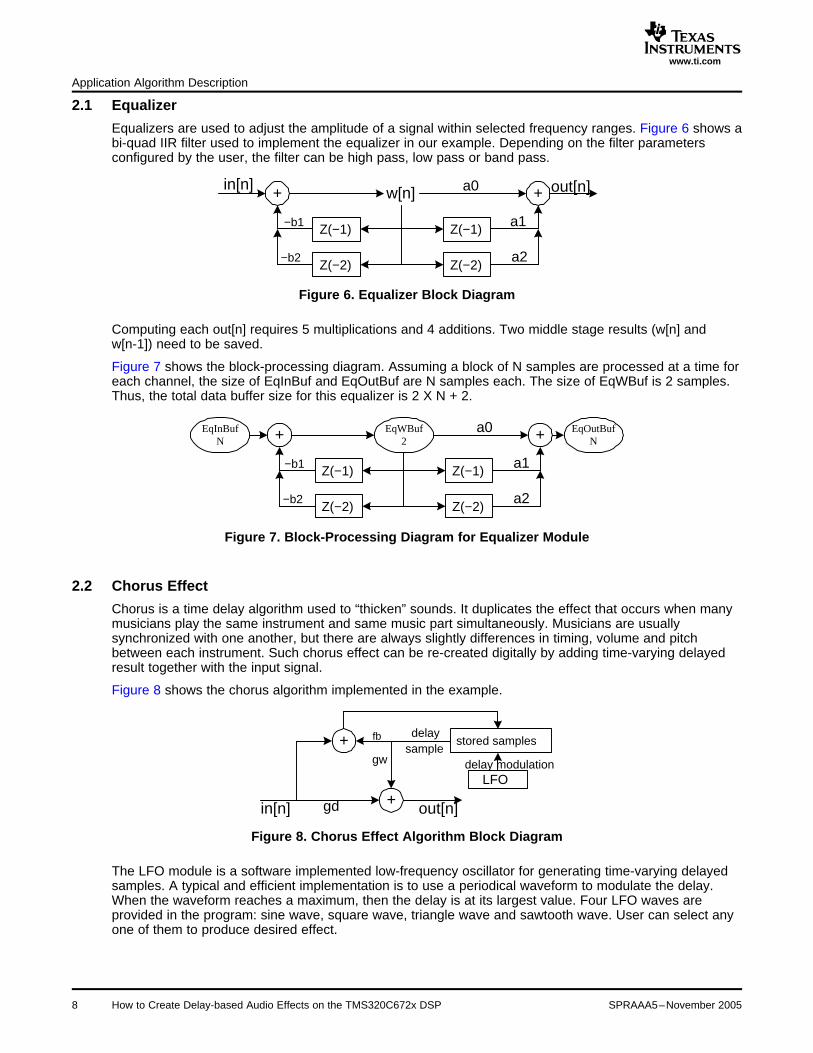
Equalizers are used to adjust the amplitude of a signal within selected frequency ranges. Figure 6 shows abi-quad IIR filter used to implement the equalizer in our example. Depending on the filter parametersconfigured by the user, the filter can be high pass, low pass or band pass.
Figure 6. Equalizer Block Diagram
Computing each out[n] requires 5 multiplications and 4 additions. Two middle stage results (w[n] andw[n-1]) need to be saved.
Figure 7 shows the block-processing diagram. Assuming a block of N samples are processed at a time foreach channel, the size of EqInBuf and EqOutBuf are N samples each. The size of EqWBuf is 2 samples.Thus, the total data buffer size for this equalizer is 2 X N + 2.
Figure 7. Block-Processing Diagram for Equalizer Module
Chorus is a time delay algorithm used to “thicken” sounds. It duplicates the effect that occurs when manymusicians play the same instrument and same music part simultaneously. Musicians are usuallysynchronized with one another, but there are always slightly differences in timing, volume and pitchbetween each instrument. Such chorus effect can be re-created digitally by adding time-varying delayedresult together with the input signal.
Figure 8 shows the chorus algorithm implemented in the example.
Figure 8. Chorus Effect Algorithm Block Diagram
The LFO module is a software implemented low-frequency oscillator for generating time-varying delayedsamples. A typical and efficient implementation is to use a periodical waveform to modulate the delay.When the waveform reaches a maximum, then the delay is at its largest value. Four LFO waves areprovided in the program: sine wave, square wave, triangle wave and sawtooth wave. User can select anyone of them to produce desired effect.
How to Create Delay-based Audio Effects on the TMS320C672x DSP8 SPRAAA5–November 2005

www.ti.com
ChoDlyBufNfb
gw
gd ChoOutBufN
ChoInBufN
(EqOutBuf)
Circularbuffer
LFO
2.3 Delay Effect
Z(−D)fb
w(n)
Z(−D)g
in[n] out[n]
Application Algorithm Description
One thing to note is that Figure 8 is a diagram showing single-sample processing, which implies onetime-varying delay value is computed for each input sample using LFO. To update the stored sample ittakes 1 multiplication and 1 addition each round. To compute each output sample, it takes 2multiplications and 1 addition. Thus, the total computation for each sample consists of 3 multiplications, 2additions and 1 LFO modulation.
Figure 9 shows the block-processing diagram for chorus. To process a block of N samples at a time, onetime-varying delay value has to be generated for each block. The generated delay is used by the dMAX topull in the block of required samples from the circular buffer using a FIFO read transfer. Three blocks ofprocessing buffers are necessary for this example:• ChoInBuf is the output from the equalizer (EqOutBuf) and the input to the chorus module.• ChoOutBuf is the output of the chorus module.• ChoDlyBuf saves the delayed samples received from the circular buffer using FIFO read before
processing starts. It is updated during the processing. After processing, it will be transferred to thecircular buffer by FIFO write.
Figure 9. Block-Processing Diagram for Chorus Module
Figure 10 shows the delay effect implemented in the example. Compared to chorus, the delay D is fixed inthis case and typically represents tens of milliseconds of delay. Compared to the equalizer shown inSection 2.1, a block of N samples can be processed at a time as long as D > N-1. This is because if D >N-1, for every block of N input samples in[n] … in[n-(N–1)], w[n-D] … w[n-D-(N–1)] are already in thecircular buffer, and thus they can be transferred to the processing buffer and processed with the inputsamples together.
Figure 10. Delay Effect Algorithm Block Diagram
Computing each w(n) and out[n] requires 2 multiplications and 2 additions. One middle stage result w[n]needs to be saved.
Figure 11 shows the block-processing diagram. Three blocks of processing buffers are necessary toprocess a block of N samples• DlyInBuf is the output from the chorus (ChoOutBuf) and input to the delay module.• DlyOutBuf is the output of the delay module• DlyWBuf saves the delay samples received from the circular buffer using a FIFO read transfer before
processing starts. The updated samples will be transferred to the circular buffer by a FIFO writetransfer.
SPRAAA5–November 2005 How to Create Delay-based Audio Effects on the TMS320C672x DSP 9

www.ti.com
DlyOutBufN
DlyWBufN
DlyInBufN
(ChoOutBuf)fb
g
FIFO read/write
2.4 Reverberation Effect
Z(−D0)ge[0]
ge[1]Z(−D1)
ge[3]
ge[2]
Z(−D3)
Z(−D2)
ge[4]
ge[5]Z(−D5)
Z(−D4)
in[n] APF 0 APF 1 APF 2 APF 3
out[n]
Z(−D5)a
Z(−APFk)b
bufA[n] lp[k]
g
fb
1−fb
in[n] out[n]−fb
APF k, k=0...3
Application Algorithm Description
Figure 11. Block-Processing Diagram for Delay Module
The reverberation algorithm simulates the effect of sound reflections in a large concert hall or room.Instead of using only a few discrete repetitions of a sound like a multi-tap delay effect, the reverb effectimplements many delayed repetitions so close together in time that the ear cannot distinguish thedifferences between the delays. The repetitions are blended together to sound continuous.
Figure 12 shows a simple reverb algorithm implemented in our example. It consists of a 6-tap echo filterand four all-pass filters (APFs).
Figure 12. Reverb Effect Block Diagram
For each input sample, the 6-tap echo filter takes 6 multiplications and 6 additions to compute an output.To update bufA[n] and lp[k] for each APF, it takes 4 multiplications and 2 additions. To compute an outputfor each APF, it takes 2 multiplications and 1 addition. The reverb output is the summation of all the APFswhich requires 4 additions. Thus, the total computation for each sample takes 30 multiplications and 28additions.
How to Create Delay-based Audio Effects on the TMS320C672x DSP10 SPRAAA5–November 2005

www.ti.com
ge[0]
ge[1]
ge[3]
ge[2]
ge[4]
ge[5]
APF 0 APF 1 APF 2 APF 3
Z(−1)a
blp[k]
g
fb
1−fb
in out−fb
APF k, k=0...3EchoDlyD5Buf
EchoDlyD4Buf
EchoDlyD3Buf
EchoDlyD2Buf
EchoDlyD1Buf
EchoDlyD0Buf
EchoInBuf
(DlyOutBuf)
RevOutBuf
APFkBuf
FIFOread
FIFO write/read
3 Implementation Considerations
Implementation Considerations
Figure 13 shows the block-processing diagram. 12 blocks of processing buffers are necessary to processa block of N samples at a time.
• EchoInBuf is the output from the delay module and input to the echo filter in the reverb module.• RevOutBuf is the output of the reverb module.• EchoDlyDkBuf (k=0…5) saves the delay samples received from the circular buffer for the echo filter.• APFkBuf (k=0…3) saves the delay samples for the APF k before processing starts from the circular
buffer. After processing, the updated samples are transmitted to the circular buffer by FIFO write.
Note: Because each APF output is computed sample by sample, no processing buffer isneeded. For each APF, only one sample for lp needs to be buffered.
Figure 13. Block-Processing Diagram for Reverb Module
The performance of an embedded system depends not only on how the hardware is designed, but also onhow the software utilizes the hardware. Generally speaking, the architecture of C672x suggests thefollowing choices to implement a delay-based audio effect algorithm such as the one described inSection 2.
• Block processing instead of single-sample processing. There are several folds of benefits from blockprocessing which will be described in Section 5. However, one thing to note is that the block size isconstrained both by the on-chip memory size and the latency requirement. The latency requirementoften imposes the more stringent limitation. For example, some professional audio systems require thelatency to be smaller than 10ms, which is about 480 sample periods for a 48-KHz sample rate. Since alatency of 20 to 100 sample periods are always caused due to the hardware limitations, i.e., the D/Aconverter latency, for this case it is safe to set the block size up to 256 samples. Too fulfill a stricterlatency requirement, the block size has to be smaller.
SPRAAA5–November 2005 How to Create Delay-based Audio Effects on the TMS320C672x DSP 11

www.ti.com
Implementation Considerations
• Saving delay samples in off-chip memory and processing samples in on-chip memory. The off-chipSDRAM has relatively larger size but significantly lower speed compared to on-chip SRAM. It can beused to store the delay samples for the algorithm. To process a block of data, it is recommended totransfer the delay samples to SRAM which runs at the same frequency as the DSP core. If thealgorithm program size is less 32KB, it can completely fit into the L1P cache.
• Moving data using dMAX.
– The FIFO transfer mode in dMAX is well designed for efficiently transferring data between a circularbuffer in the SDRAM and a processing buffer in the SRAM. One obvious benefit is that DSP can beused to do the processing work while dMAX is transferring the data. Compared to the EDMAarchitecture in some other C6000 DSPs, the FIFO transfer feature of dMAX has another advantagefor audio systems. Imagine using EDMA to perform the transfer shown in Figure 4, which wouldrequire the use of four linked 1-D transfers*. However, since the circular buffer’s read/write pointersare not updated by EDMA automatically, the DSP must manually update them. Also, every time atransfer is completed the DSP needs to update the source/destination address for each block.Things get even worse if one block rolls over from the bottom to the top of the circular buffer,because the transfer has to be manually split into two transfers.
Note: It is not always possible to use a 2-D EDMA transfer in this case because it is oftenT!=D1 !=D2.
– For any FIFO transfer, rolling over the read/write pointer in the middle of a block transfer should beavoided as much as possible. Although dMAX can automatically handle this situation by it splittingone transfer into two, this increases the transfer overhead. To avoid this situation, it isrecommended to make the circular buffer size a multiple of the processing block size. Also, theread/write pointer should be aligned to the processing block size. This ensures that the read/writepointer will only be rolled over in-between block transfers.
– The dMAX general purpose transfer is designed to efficiently transfer input/output audio samplesto/from memory. The general purpose transfer can automatically de-multiplex/multiplex samples ofdifferent channels from/to the same serial port.
• Pipelined processing. The dMAX in the C672x is naturally designed to support a PING-PONG bufferscheme for pipelined processing. While the DSP is processing the PING (PONG) buffer, data can betransferred to/from the PONG (PING) buffer for the next round of processing.
How to Create Delay-based Audio Effects on the TMS320C672x DSP12 SPRAAA5–November 2005

www.ti.com
3.1 Buffer Organization
Implementation Considerations
Section 2 explained the necessary processing buffers for each effect module to be implemented. Table 1summarizes these processing buffers. Please refer to Figure 5 for all the effect modules.
Table 1. Processing Buffer Summary
Buffer Name Description
InBuf, EqInbuf This is the buffer used to receive the input samples from the McASP and also serves as the input bufferto the equalizer module.
EqOutBuf, ChoInBuf This is the output buffer for the equalizer module and also the input buffer for the chorus module.
ChoDlyBuf This buffer saves the delay samples received from the circular buffer for the chorus module using FIFOread before processing starts. After processing, the updated ones will be transferred to the circular bufferby FIFO write.
ChoOutBuf, DlyInBuf This is the output buffer for the chorus module and also the input buffer for the delay module.
DlyWBuf This buffer saves the delay samples received from the circular buffer for the delay module using FIFOread before processing starts. After processing, The updated samples will be transferred to the circularbuffer by FIFO write.
DlyOutBuf, EchoInBuf This is the output buffer for the delay module and also the input buffer for the echo filter in the reverbmodule.
EchoDlyDkBuf, K=0…5 These 6 buffers save the delay samples received from the circular buffer for the echo filter in the reverbmodule before processing starts.
APFkBuf, k=0…3 These 4 buffers save the delay samples received from the circular buffer for the 4 APFs in the reverbmodule before processing starts. After processing, The updated samples will be transferred to thecircular buffer by FIFO write.
OutBuf, RevOutBuf This is the output buffer of the reverb module. It also serves as the output buffer for the system totransmit output samples to the McASP.
Since we separate the left and right channels and use PING-PONG buffer scheme, 4x the number ofprocessing buffers are needed. To identify a particular buffer for a particular channel in the particularPING/PONG set, we use the following naming convention in the rest of the document.
[SET = PING or PONG]_"buffer name"_[CHAN = L or R]
For example, to refer to the input buffer to the equalizer module of the left channel in the PING set, weuse PING_L_EqInbuf.
Figure 14 shows all the processing buffers which reside in on-chip SRAM.
For the buffers in pattern 1, data is transferred between the buffers and the circular buffer bi-directionallyusing dMAX FIFO read and FIFO Write Transfers.
For the buffers in pattern 2, data is transferred to the buffers from the circular buffer by dMAX FIFO readtransfer.
For the buffers in pattern 3, data is transferred between the buffers and the McASP by dMAX generalpurpose transfers.
For the buffers in pattern 4, no dMAX transfers are involved.
SPRAAA5–November 2005 How to Create Delay-based Audio Effects on the TMS320C672x DSP 13

www.ti.com
���������������������������������������������������������������������������������������������������������������������
����������������������PING_L_ChoDlyBuf����������������������PING_L_DlyWBuf
PING_L_EchoDlyD0Buf
buffers related to FIFO read/write (PING set)
PING_L_EqOutBuf
PING_R_EqOutBuf
PONG_L_EqOutBuf
PONG_R_EqOutBuf
����������������������PING_L_APF0Buf����������������������PING_L_APF1Buf�����������
PING_L_APF2Buf
����������������������
PING_L_APF3Buf
����������������������PING_R_APF1Buf����������������������PING_R_APF2Buf�����������
PING_R_APF3Buf
����������������������
PING_R_APF0Buf
buffers related to FIFO read/write (PONG set)
����������������������
PING_L_dlyOutBuf
PING_L_InBuf
PING_R_InBufPONG_L_InBuf
PONG_R_InBuf
PING_L_OutBuf
PING_R_OutBuf
PONG_L_OutBuf
PONG_R_OutBuf
PING_L_DlyInBuf
PING_R_DlyInBuf
PONG_L_DlyInBuf
PONG_R_DlyInBuf
PING_L_EchoDlyD1Buf
PING_L_EchoDlyD2Buf
PING_L_EchoDlyD3Buf
PING_L_EchoDlyD4Buf
PING_L_EchoDlyD5Buf
�����������PING_R_ChoDlyBuf
����������������������
PING_R_DlyWBuf
PING_R_EchoDlyD0Buf
PING_R_EchoDlyD1Buf
PING_R_EchoDlyD2Buf
PING_R_EchoDlyD3Buf
PING_R_EchoDlyD4Buf
PING_R_EchoDlyD5Buf
����������������������
PING_R_dlyOutBuf
Left channel Right channel
����������������������PONG_L_ChoDlyBuf����������������������PONG_L_DlyWBuf
PONG_L_EchoDlyD0Buf
����������������������PONG_L_APF0Buf����������������������PONG_L_APF1Buf�����������
PONG_L_APF2Buf
����������������������
PONG_L_APF3Buf
����������������������PONG_R_APF1Buf����������������������PONG_R_APF2Buf�����������
PONG_R_APF3Buf
����������������������
PONG_R_APF0Buf
����������������������
PONG_L_dlyOutBuf
PONG_L_EchoDlyD1Buf
PONG_L_EchoDlyD2Buf
PONG_L_EchoDlyD3Buf
PONG_L_EchoDlyD4Buf
PONG_L_EchoDlyD5Buf
�����������PONG_R_ChoDlyBuf
����������������������
PONG_R_DlyWBuf
PONG_R_EchoDlyD0Buf
PONG_R_EchoDlyD1Buf
PONG_R_EchoDlyD2Buf
PONG_R_EchoDlyD3Buf
PONG_R_EchoDlyD4Buf
PONG_R_EchoDlyD5Buf
����������������������
PONG_R_dlyOutBuf
Left channel Right channel
�����������pattern 1 pattern 2
���������pattern 3 pattern 4
Implementation Considerations
Figure 14. Processing Buffer Organization
There are seven sections for each channel in the circular buffer. Due to processing separation for the leftand right channel, the number of sections in the circular buffer is 14 in total. For each channel, the datasections to be saved in the circular buffer include:
1. Delay line for the chorus module. Before a round of processing starts, delay samples are transferred toChoDlyBuf by FIFO read. After processing, updated samples are transferred from ChoDlyBuf to it byFIFO write. We use L_ChoDlySect and R_ChoDlySect to denote this section for the left and rightchannel, respectively.
2. Delay line for the delay module. Before a round of processing starts, delay samples are transferred toDlyWBuf by FIFO read. After processing, updated samples are transferred from DlyWBuf to it by FIFOwrite. We use L_DlyWSect and R_DlyWSect to denote this section for the left and right channel,respectively.
3. Delay line for the echo filter in the reverb module. Before a round of processing starts, delay samplesare transferred to EchoDlyDkBuf (k=0…5) by FIFO read. After processing, latest samples in EchoInBufare transferred to it by FIFO write. We use L_EchoDlySect and R_EchoDlySect to denote this sectionfor the left and right channel, respectively.
4. Delay line for each APFk (k=0…3) in the reverb module. Before a round of processing starts, delaysamples are transferred to APFkBuf by FIFO read. After processing, updated samples are transferredfrom APFkBuf to it by FIFO write. We use L_APFkSect and R_APFkSect to denote this section for theleft and right channel, respectively.
Since a delay line often needs to keep tens of thousands of samples, the circular buffer is put in SDRAM.The following figure shows the circular buffer organization.
How to Create Delay-based Audio Effects on the TMS320C672x DSP14 SPRAAA5–November 2005

www.ti.com
Left channel Right channel
Read/write pointer
Sect 6:L_DlyWSect
delay samplesfor delaySect 5:
L_Cho_DlySect:delay samples
for chorus
Sect 3: L_APF2Sectdelay samples
for APF2 in reverb
Sect 1:L_APF0Sect
delay samplesfor APF0in reverb
Sect 0:L_EchoDlySectdelay samplesfor echo filter
in reverb
Sect 13:R_EchoDlySectdelay samplesfor echo filter
in reverb
Sect 12:R_APF3Sect
delay samplesfor APF3in reverb
Sect 11: R_APF2Sectdelay samples for
APF2 inreverb
Sect 2: L_APF1Sectdelay samples for
APF1 inreverb
delay samplesfor APF1 in reverb
Sect 10: R_APF1Sect
Sect 4:L_APF3Sect delaysamples for APF3
in reverbsamples for APF0R_APF0Sect delay
in reverb
Sect 9:
R_DlyWSect:delay samples
for delay
Sect 8:delay samples
for chorus
R_ChoDlySectSect 7:
Implementation Considerations
Figure 15. Circular Buffer Organization
In each processing round for a FIFO write transfer, seven blocks for the left channel and seven blocks forthe right channel need to be transferred to the circular buffer. Table 2 shows the entry values in the FIFOwrite transfer’s delay table in which size(“section name”) denotes the size of a particular section.
SPRAAA5–November 2005 How to Create Delay-based Audio Effects on the TMS320C672x DSP 15

www.ti.com
FIFO write, count0 = N, count1 = 14, index0=1, index1=1
left channel right channel
write pointer
sect 0:L_EchoDlySectdelay samplesfor echo filter
in reverb
sect 1:L_APF0Sect
delaysamples
for APF0 inreverb
sect 2:L_APF1Sect
delay samplesfor APF1 in
reverb
sect 4:L_APF3Sect
delay samplesfor APF3 in
reverb
sect 5:L_ChoDlySect:delay samples
for chorus
sect 6:L_DlyWSectdelay samples
for delay
sect 12:R_APF3Sectdelay samplesfor APF3 in
reverb
sect 11:R_APF2Sect
delay samples forAPF2 in reverb
sect 10:R_APF1Sectdelay samples
for APF1 in rever
sect 9:R_APF0Sectdelay samplesfor APF0 in
reverb
sect 8:R_DlyWSectdelay samples
for delay
sect 7:R_ChoDlySectdelay samples
for chorus
contiguous memory
sect 3:L_APF2Sectdelay samplesfor APF2 in
reverb
sect 13:R_EchoDlySectdelay samplesfor echo filter
in reverb���������PING_L_ChoDlyBuf������������������PING_L_DlyWBuf
PING_L_EchoDlyD0Buf
������������������PING_L_APF0Buf���������
PING_L_APF1Buf
������������������
PING_L_APF2Buf������������������PING_L_APF3Buf
���������PING_L_DlyOutBuf
PING_L_EchoDlyD1Buf
PING_L_EchoDlyD2Buf
PING_L_EchoDlyD3Buf
PING_L_EchoDlyD4Buf
PING_L_EchoDlyD5Buf
���������PING_R_APF1Buf
������������������
PING_R_APF2Buf������������������PING_R_APF3Buf
������������������PING_R_APF0Buf
������������������PING_R_ChoDlyBuf���������
PING_R_DlyWBuf
PING_R_EchoDlyD0Buf
PING_R_EchoDlyD1Buf
PING_R_EchoDlyD2Buf
PING_R_EchoDlyD3Buf
PING_R_EchoDlyD4Buf
PING_R_EchoDlyD5Buf
���������PING_R_DlyOutBuf
Implementation Considerations
Table 2. FIFO Write Delay Table Values
Entry ID Entry Value Comment
FIFOW_Entry[0] 0 Transfer from L_EchoInBuf
FIFOW_Entry[1] size(L_EchoDlySect) Transfer from L_APF0Buf
FIFOW_Entry[2] FIFOW_Entry[1] + size(L_APF0Sect) Transfer from L_APF1Buf
FIFOW_Entry[3] FIFOW_Entry[2] + size(L_APF1Sect) Transfer from L_APF2Buf
FIFOW_Entry[4] FIFOW_Entry[3] + size(L_APF2Sect) Transfer from L_APF3Buf
FIFOW_Entry[5] FIFOW_Entry[4] + size(L_APF3Sect) Transfer from L_ChoDlyBuf
FIFOW_Entry[6] FIFOW_Entry[5] + size(L_ChoDlySect) Transfer from L_DlyWBuf
FIFOW_Entry[7] FIFOW_Entry[6] + size(L_DlyWSect) Transfer from R_ChoDlyBuf
FIFOW_Entry[8] FIFOW_Entry[7] + size(R_ChoDlySect) Transfer from R_DlyWBuf
FIFOW_Entry[9] FIFOW_Entry[8] + size(R_DlyWSect) Transfer from R_APF0Buf
FIFOW_Entry[10] FIFOW_Entry[9] + size(R_APF0Sect) Transfer from R_APF1Buf
FIFOW_Entry[11] FIFOW_Entry[10] + size(R_APF1Sect) Transfer from R_APF2Buf
FIFOW_Entry[12] FIFOW_Entry[11] + size(R_APF2Sect) Transfer from R_APF3Buf
FIFOW_Entry[13] FIFOW_Entry[12] + size(R_APF3Sect) Transfer from R_EchoInBuf
Figure 16 shows how a FIFO write transfer fills the circular buffer from the PING set processing buffers.Again, since a FIFO write transfer requires index0 and index1 to be fixed, we place all the processingbuffers associated with FIFO write contiguously so that index1 = 1.
Figure 16. FIFO Write
How to Create Delay-based Audio Effects on the TMS320C672x DSP16 SPRAAA5–November 2005

www.ti.com
Implementation Considerations
In a processing round for a FIFO read transfer, 13 blocks for data for each channel need to be transferredfrom the circular buffer to the processing buffers. Table 3 shows the entry values in the FIFO readtransfer's delay table.
Table 3. FIFO Read Delay Table Values
Entry ID Entry Value Comment
FIFOR_Entry[0] L_D0 Transfer from L_EchoDlySect to L_EchoDlyD0Buf. L_D0 is the1st delay tap for the echo filter of the left channel.
FIFOR_Entry[1] L_D1 Transfer from L_EchoDlySect to L_EchoDlyD1Buf. L_D1 is the2nd delay tap for the echo filter of the left channel.
FIFOR_Entry[2] L_D2 Transfer from L_EchoDlySect to L_EchoDlyD2Buf. L_D2 is the3rd delay tap for the echo filter of the left channel.
FIFOR_Entry[3] L_D3 Transfer from L_EchoDlySect to L_EchoDlyD3Buf. L_D3 is the4th delay tap for the echo filter of the left channel.
FIFOR_Entry[4] L_D4 Transfer from L_EchoDlySect to L_EchoDlyD4Buf. L_D4 is the5th delay tap for the echo filter of the left channel.
FIFOR_Entry[5] L_D5 Transfer from L_EchoDlySect to L_EchoDlyD0Buf. L_D5 is the6th delay tap for the echo filter of the left channel.
FIFOR_Entry[6] L_D5 Transfer from L_EchoDlySect to L_DlyOutbuf. It is anunnecessary transfer.
FIFOR_Entry[7] FIFOW_Entry[1] + L_APF0Dly Transfer from L_APF0Sect to L_APF0Buf. L_APF0Dly is thedelay tap for the APF 0 of the left channel.
FIFOR_Entry[8] FIFOW_Entry[2] + L_APF1Dly Transfer from L_APF1Sect to L_APF1Buf. L_APF1Dly is thedelay tap for the APF 1 of the left channel.
FIFOR_Entry[9] FIFOW_Entry[3] + L_APF2Dly Transfer from L_APF2Sect to L_APF2Buf. L_APF2Dly is thedelay tap for the APF 2 of the left channel.
FIFOR_Entry[10] FIFOW_Entry[4] + L_APF3Dly Transfer from L_APF3Sect to L_APF3Buf. L_APF3Dly is thedelay tap for the APF 3 of the left channel.
FIFOR_Entry[11] FIFOW_Entry[5] + L_ChoDly Transfer from L_ChoDlySect to L_ChoDlyBuf. L_ChoDly is thedelay (modulated by LFO) for the chorus of the left channel.
FIFOR_Entry[12] FIFOW_Entry[6] + L_DlyD Transfer from L_DlyWSect to L_DlyWBuf. L_DlyD is the delayfor the delay module of the left channel.
FIFOR_Entry[13] FIFOW_Entry[7] + R_ChoDly Transfer from R_ChoDlySect to R_ChoDlyBuf. R_ChoDly is thedelay (modulated by LFO) for the chorus of the right channel.
FIFOR_Entry[14] FIFOW_Entry[8] + R_DlyD Transfer from R_DlyWSect to R_DlyWBuf. R_DlyD is the delayfor the delay module of the right channel.
FIFOR_Entry[15] FIFOW_Entry[9] + R_APF0Dly Transfer from R_APF0Sect to R_APF0Buf. R_APF0Dly is thedelay tap for the APF 0 of the right channel.
FIFOR_Entry[16] FIFOW_Entry[10] + R_APF1Dly Transfer from R_APF1Sect to R_APF1Buf. R_APF1Dly is thedelay tap for the APF 1 of the right channel.
FIFOR_Entry[17] FIFOW_Entry[11] + R_APF2Dly Transfer from R_APF2Sect to R_APF2Buf. R_APF2Dly is thedelay tap for the APF 2 of the right channel.
FIFOR_Entry[18] FIFOW_Entry[12] + R_APF3Dly Transfer from R_APF3Sect to R_APF3Buf. R_APF3Dly is thedelay tap for the APF 3 of the right channel.
FIFOR_Entry[19] FIFOW_Entry[13] + R_D0 Transfer from R_EchoDlySect to R_DlyOutbuf. It is anunnecessary transfer.
FIFOR_Entry[20] FIFOW_Entry[13] + R_D0 Transfer from R_EchoDlySect to R_EchoDlyD0Buf. R_D0 is the1st delay tap for the echo filter of the right channel.
FIFOR_Entry[21] FIFOW_Entry[13] + R_D1 Transfer from R_EchoDlySect to R_EchoDlyD1Buf. R_D1 is the2nd delay tap for the echo filter of the right channel.
FIFOR_Entry[22] FIFOW_Entry[13] + R_D2 Transfer from R_EchoDlySect to R_EchoDlyD2Buf. R_D2 is the3rd delay tap for the echo filter of the right channel.
FIFOR_Entry[23] FIFOW_Entry[13] + R_D3 Transfer from R_EchoDlySect to R_EchoDlyD3Buf. R_D3 is the4th delay tap for the echo filter of the right channel.
FIFOR_Entry[24] FIFOW_Entry[13] + R_D4 Transfer from R_EchoDlySect to R_EchoDlyD4Buf. R_D4 is the5th delay tap for the echo filter of the right channel.
FIFOR_Entry[25] FIFOW_Entry[13] + R_D5 Transfer from R_EchoDlySect to R_EchoDlyD5Buf. R_D5 is the6th delay tap for the echo filter of the right channel.
SPRAAA5–November 2005 How to Create Delay-based Audio Effects on the TMS320C672x DSP 17

www.ti.com
Left channel Right channel
Sect 6:L_DlyWSect
delay samplesfor delaySect 5:
L_Cho_DlySect:delay samples
for chorus
Sect 3: L_APF2Sectdelay samples
for APF2 in reverb
Sect 1:L_APF0Sect
delay samplesfor APF0in reverb
Sect 0:L_EchoDlySectdelay samplesfor echo filter
in reverb
Sect 13:R_EchoDlySectdelay samplesfor echo filter
in reverb
Sect 12:R_APF3Sect
delay samplesfor APF3in reverb
Sect 11: R_APF2Sectdelay samples for
APF2 inreverb
Sect 2: L_APF1Sectdelay samples for
APF1 inreverb
delay samplesfor APF1 in reverb
Sect 10: R_APF1Sect
Sect 4:L_APF3Sect delaysamples for APF3
in reverbsamples for APF0
R_APF0Sect delay
in reverb
Sect 9:
R_DlyWSect:delay samples
for delay
Sect 8:delay samples
for chorus
R_ChoDlySectSect 7:
PING_L_EchoDlyD0BufPING_L_EchoDlyD1Buf
PING_L_EchoDlyD3Buf
PING_L_EchoDlyD2Buf
PING_L_EchoDlyD4Buf
PING_L_EchoDlyD5Buf
PING_L_DlyWBufPING_L_ChoDlyBuf
PING_L_APF1Buf
PING_L_APF2Buf
PING_L_APF0Buf
PING_L_dlyOutBuf
PING_R_DlyWBufPING_R_ChoDlyBuf
PING_R_APF1BufPING_R_APF0Buf
PING_R_dlyOutBuf
PING_R_APF2Buf
PING_R_EchoDlyD0BufPING_R_EchoDlyD1Buf
PING_L_APF3Buf
PING_R_APF3Buf
PING_R_EchoDlyD3Buf
PING_R_EchoDlyD4BufPING_R_EchoDlyD5Buf
PING_R_EchoDlyD2Buf
UnnecessaryFIFO read
UnnecessaryFIFO read
Contiguous memory
Read/writepointer
FIFO red, count0=N, count1=26, index0=1, index1=1
Implementation Considerations
Figure 17. FIFO Read
Figure 17 shows how a FIFO read transfer fills the PING set processing buffers. A FIFO readtransfer requires index0 and index1 to be fixed for all blocks, which is why we put all the processingbuffers associated with FIFO read contiguously so that index1 = 1.
L_DlyOutBuf and R_DlyOutBuf are actually for saving the output of delay modules and do not needto be filled by FIFO read (see the dash lines arrows in Figure 17). However, the data in them needto be transferred to circular buffer by the FIFO write transfer. By putting them in such places andcopying two extra buffers, only one FIFO read transfer (and thus only one interrupt) is necessary tofill all the necessary processing buffers for two channels. Otherwise, two FIFO transfers (one foreach channel) are needed. Since usually the processing buffer size is small (about 4 - 256samples) for targeted application, the performance will gain by reducing an interrupt.
Copying extra buffers is not the only method to save an interrupt as described above. In theprovided application, we encounter such a scenario because we want to separate the processingbuffers for each channel to give user a clear view. The following are general guidance of how toplace the processing buffers in order.
For each PING or PONG set,
1. For all the processing buffers involved with FIFO read only
a. Place them contiguously.b. Place all the buffers accessing the same section in the circular buffer contiguously.c. Record the order of the circular buffer section.
2. For all the processing buffers involved with FIFO write only
a. Place them contiguously. The order is the same as the one recorded in 1-c.3. For all the processing buffers involved with both FIFO read and write
a. Place them contiguously.b. Place all the buffers accessing the same section in the circular buffer contiguously.
4. Place 3 between 1 and 2.
How to Create Delay-based Audio Effects on the TMS320C672x DSP18 SPRAAA5–November 2005

www.ti.com
sect 1:R_EchoDlySectdelay samplesfor echo filter
in reverb
sect 9:R_APF3Sectdelay samplesfor APF3 in
reverb
sect 12:L_DlyWSectdelay samples
for delay
sect 8:R_APF2Sectdelay samples
for APF2in reverb
sect 7:R_APF1Sectdelay samplesfor APF1 in
reverb
sect 6:R_APF0Sectdelay samplesfor APF0 in
reverb
sect 13:R_DlyWSectdelay samples
for delay
sect 11:R_ChoDlySectdelay samples
for chorus
sect 0:L_EchoDlySectdelay samplesfor echo filter
in reverb
sect 2:L_APF0Sect
delay samplesfor APF0 in
reverb
sect 3:L_APF1Sect
delay samplesfor APF1 in
reverb
sect 5:L_APF3Sectdelay samplesfor APF3 in
reverb
sect 10:L_ChoDlySect:delay samples
for chorus
sect 4:L_APF2Sect
delay samplesfor APF2 in
reverb
FIF
O r
ead
& w
rite
FIF
O w
rite
only
������������������PING_L_ChoDlyBuf������������������PING_L_DlyWBuf
PING_L_EchoDlyD0Buf
working buffer placement (PING set)PONG set is the same
������������������PING_L_APF0Buf���������
PING_L_APF1Buf
������������������
PING_L_APF2Buf������������������PING_L_APF3Buf������������������PING_R_APF1Buf���������
PING_R_APF2Buf
������������������
PING_R_APF3Buf
���������PING_R_APF0Buf
������������������
PING_L_DlyOutBuf
PING_L_EchoDlyD1Buf
PING_L_EchoDlyD2Buf
PING_L_EchoDlyD3Buf
PING_L_EchoDlyD4Buf
PING_L_EchoDlyD5Buf
���������PING_R_ChoDlyBuf���������PING_R_DlyWBuf
PING_R_EchoDlyD0Buf
PING_R_EchoDlyD1Buf
PING_R_EchoDlyD2Buf
PING_R_EchoDlyD3Buf
PING_R_EchoDlyD4Buf
PING_R_EchoDlyD5Buf ������������������PING_R_dlyOutBuf
FIF
O r
ead
only
read pointer
write pointer
pattern 2
���������pattern 1
������������������pattern 3
Implementation Considerations
5. The section order of the circular buffer follows the processing buffer orders.6. For those processing buffers not involved with FIFO transfer, we do not care about their
placement order.
For example, an optimized processing buffer placement order for this application is shown inFigure 18.
Figure 18. Optimized Processing Buffer Organization
All the buffers in pattern 2 are involved with FIFO read transfer only and are placed contiguously(rule 1-a).
PING_L_EchoDlyDkBuf (k=0…5) receive samples from L_EchoDlySect and they are placedcontiguously (rule 1-b). PING_R_EchoDlyDkBuf receive samples from R_EchoDlySect and areplaced contiguously too (rule 1-b).
The order of the involved circular buffer sections is L_EchoDlySect -> R_EchoDlySect (rule 1-c).
PING_R_DlyOutBuf and PING_L_DlyOutBuf (in pattern 3) are involved with FIFO write only andare placed contiguously. Their order is the same as L_EchoDlySect -> R_EchoDlySect (rule 2-a).
All the buffers in pattern 1 are involved with both FIFO read and write. They are put contiguously(rule 3-a). Since each one corresponds to a section in the circular buffer, rule 3-b is automaticallymet.
All the buffers in pattern 1 are placed between the ones in pattern 2 and the ones in pattern 3 (rule4).
The section order in the circular buffer is shown in Figure 18. It is the same order as the processingbuffers (rule-5).
Table 4 and Table 5 show the one-to-one correspondence between the circular buffer sections andprocessing buffers for the FIFO read and FIFO write transfer.
SPRAAA5–November 2005 How to Create Delay-based Audio Effects on the TMS320C672x DSP 19
www.ti.com
Implementation Considerations
Table 4. Optimized FIFO Read Between the Circular Buffer and Processing Buffers
Processing Buffers Data Direction Sections in the CircularBuffer
PING_L_EchoDlyDkBuf (k=0...5) ← Sect 0: L_EchoDlySect
PING_R_EchoDlyDkBuf (k=0...5) ← Sect 1: R_EchoDlySect
PING_L_APF0Buf ← Sect 2: L_APF0Sect
PING_L_APF1Buf ← Sect 3: L_APF1Sect
PING_L_APF2Buf ← Sect 4: L_APF2Sect
PING_L_APF3Buf ← Sect 5: L_APF3Sect
PING_R_APF0Buf ← Sect 6: R_APF0Sect
PING_R_APF1Buf ← Sect 7: R_APF1Sect
PING_R_APF2Buf ← Sect 8: R_APF2Sect
PING_R_APF3Buf ← Sect 9: R_APF3Sect
PING_L_ChoDlyBuf ← Sect 10: L_ChoDlySect
PING_R_ChoDlyBuf ← Sect 11: R_ChoDlySect
PING_L_DlyWBuf ← Sect 12: L_DlyWSect
PING_R_DlyWBuf ← Sect 13: L_DlySect
Table 5. Optimized FIFO Write Between the Circular Buffer and Processing Buffers
Processing Buffers Data Direction Sections in the CircularBuffer
PING_L_APF0Buf → Sect 2: L_APF0Sect
PING_L_APF1Buf → Sect 3: L_APF1Sect
PING_L_APF2Buf → Sect 4: L_APF2Sect
PING_L_APF3Buf → Sect 5: L_APF3Sect
PING_R_APF0Buf → Sect 6: R_APF0Sect
PING_R_APF1Buf → Sect 7: R_APF1Sect
PING_R_APF2Buf → Sect 8: R_APF2Sect
PING_R_APF3Buf → Sect 9: R_APF3Sect
PING_L_ChoDlyBuf → Sect 10: L_ChoDlySect
PING_R_ChoDlyBuf → Sect 11: R_ChoDlySect
PING_L_DlyWBuf → Sect 12: L_DlyWSect
PING_R_DlyWBuf → Sect 13: L_DlyWSect
PING_L_DlyOutBuf → Sect 0: L_EchoDlySect
PING_R_DlyOutBuf → Sect 1: R_EchoDlySect
How to Create Delay-based Audio Effects on the TMS320C672x DSP20 SPRAAA5–November 2005

www.ti.com
3.2 PING-PONG Scheme
process PINGprocessing
bufs
FIFO writePING set processingbufs −−> circular buf.
FIFO readcircular buf. −−> PONGset processing buffers
process PONGprocessing
bufs
FIFO writePONG set processingbufs −−> circular buf.
FIFO readcircular buf. −−> PING set
processing buffers
McASP_in −−> PONG set input buffers
PONG set output bufs −−> McASP_out
triggerFIFOread
triggerFIFOwrite
triggerFIFOread
triggerFIFOwrite
McASP_in −−> PING set input buffers
PING set output bufs −−> McASP_outPING set output
bufs −−>
McASP_out
interrrupt
dMAX eventdMAXtask
CPUtask
event 5/7/9 (McASP0/1/2 RX event)
depending on which McASP being used
CPU triggered event (event 0/1/17/18/23/
24/30/31 depending on which one is used)
Also a CPU triggered event which cannot
be the same as the one triggers FIFO read
event 4/6/8 (McASP0/1/2 TX event)
depending on which McASP being used
Implementation Considerations
Figure 19 illustrates how the PING-PONG buffer scheme works.
Figure 19. PING-PONG Buffer Scheme Flow
1. CPU starts processing the data in the PING (PONG) set processing buffers after the following fourtransfers are completed. Transfer a is the last one to finish.
a. A block of input samples are transferred from McASP_in to PING (PONG) input buffers by dMAX.The input samples will be processed by the CPU.
b. All the PING (PONG) set processing buffers associated with FIFO read have been filled by dMAX.These buffers will be used with input samples for processing by the CPU.
c. The circular buffer has been updated in the last round. It is updated by a FIFO write whichtransfers data from associated PONG (PING) set processing buffers to the circular buffer.
d. The output samples (which are generated during the one before the last round) in the PING(PONG)` set output buffer have been transferred to McASP_out.
2. When CPU starts processing the data in the PING (PONG) set processing buffer, another FIFO read istriggered by CPU to prepare for the processing buffers for the next round. dMAX will perform thetransfer to fill the PONG (PING) set processing buffers associated with FIFO read.
3. After CPU finishes processing the PING (PONG) set data, the output data are put in the PING (PONG)set output buffer which will be transferred to McASP_out by dMAX when the previous transfer iscompleted. Meanwhile, another FIFO write is triggered by CPU to update the circular buffer. The newdata in the PING (PONG) set processing buffers associated with FIFO write are transferred to thecircular buffer by dMAX.
The PING-PONG scheme described above assumes that the following conditions are met.
t( get_input_block ) > t( FIFO_read )
where t( get_input_block ) is the time interval to transfer a block of input samples from McASP_in to theinput processing buffer, and t( FIFO_read ) is the time interval for a FIFO Read Transfer.
t( get_input_block ) > t( processing ) + t( FIFO_write )
SPRAAA5–November 2005 How to Create Delay-based Audio Effects on the TMS320C672x DSP 21

www.ti.com
msMHz 1664.0150303226 =××
, where 26 is the number of blocks to be transferred.
msKHz 6667.096322 =×
The FIFO Write Transfer will takemsMHz 0896.0150
303214 =××, where 14 is the number of blocks to
4 Pseudo Code Example
Pseudo Code Example
where t( processing ) is the time interval DSP takes to process 2 blocks (one for left and one for rightchannel) of input samples, and t( FIFO_write ) is the time interval for a FIFO Write Transfer.
Given the audio sample rate as 96-KHz, we can show that these two conditions can easily be met onC672x.
Let us assume that it takes 30* dMAX cycles in average to move a sample between on-chip SRAM andSDRAM. Given the dMAX frequency is 150-MHz, for a block of size 32, the FIFO Read Transfer takes
Note: An experiment shows that to transfer a block of 32 sequential samples (each of which is32-bit) between the SDRAM and internal memory, it takes about 273 dMAX cycles if theQTSL is set to 16 and there is no resource competition. Here, we loosely assume it takes30 dMAX cycles in average to transfer per sample to take into account the fact that FIFOread and FIFO write transfer may compete for accessing the SDRAM and internalmemory.
To transfer two input blocks from McASP_in to the input processing buffers, it takes
Thus, the 1st condition can be easily met.
be written to the circular buffer. Thus, the number of DSP cycles left for processing is (0.6667ms -0.0896ms) x 300 MHz = 0.17313 x 10⁶ cycles. For fully optimized code on C672x, computing the productof two 32-element floating vectors takes less than 50 cycles. Thus, the cycles left for processing are morethan enough for the example application.
The following pseudo code example shows the overall application behavior.
Example 1. Pseudo Code
Variables:Int currWkBufs; // the current buffer being processed, PING or PONGInt currInBuf; // the current input buffer being processed, PING or PONGInt currOutBuf; // the current output buffer being processed, PING or PONGInt allBufRdyFlg; // flag indicating buffer transfer status:
// input, output, FIFO write, FIFO readFunction:// application kernel functionvoid app() {
app_start:// wait for the following events:// a new frame of input samples are received;// the previous frame of output samples are transmitted// the circular buffer has been updated (triggered in the previous round)// the processing buffer has been filled (triggered in the previous round)while ( !allBufRdyFlg );allBufRdyFlg = 0; // clean the flagif ( parameters_changed() )apply_change(); // if any parameter is changed by user, apply the change.
// decide which set to be processed and updatedSWITCH_PINGPONG( currWkBufs ); // the set to be computedSWITCH_PINGPONG( nextWkBufs ); // the set to be filled by FIFO read for the
// next round
How to Create Delay-based Audio Effects on the TMS320C672x DSP22 SPRAAA5–November 2005

www.ti.com
Pseudo Code Example
Example 1. Pseudo Code (continued)
// trigger FIFO read to prepare processing buffers for next roundtrigger_FIFO_read( nextWkBufs );
// call equalizer module for left and right channelif ( parameter_changed( eqParamL ) )equalizer_design( eqParamL ); // translate the parameters for the algorithm
equalizer( inputBufL[currInBuf], eqOutL[currWkBufs] );if ( parameter_changed( eqParamR ) )equalizer_design( eqParamR ); // translate the parameters for the algorithm
equalizer( inputBufR[currInBuf], eqOutR[currWkBufs] );
// call chorus for left and right channelif ( parameter_changed( choParamL ) )chorus_design( choParamL ); // translate the parameters for the algorithm
chorus( eqOutL[currWkBufs], choDlyL[currWkBufs], choOutL[currWkBufs] );if ( parameter_changed( choParamR ) )chorus_design( choParamR ); // translate the parameters for the algorithm
chorus( eqOutR[currWkBufs], choDlyR[currWkBufs], choOutR[currWkBufs] );
// call delay for left and right channelif ( parameter_changed( dlyParamL ) )delay_design( dlyParamL ); // translate the parameters for the algorithm
delay( choOutL[currWkBufs], dlyWL[currWkBufs], dlyOutL[currWkBufs] );if ( parameter_changed( dlyParamR ) )delay_design( dlyParamR ); // translate the parameters for the algorithm
delay( choOutR[currWkBufs], dlyWR[currWkBufs], dlyOutR[currWkBufs] );// call reverb for left and right channelif ( parameter_changed( revParamL ) )reverb_design( revParamL ); // translate the parameters for the algorithm
reverb( dlyOutL[currWkBufs], echoDlyL[currWkBufs][6],apfDlyL[currWkBufs][4], outputBufL[currOutBuf] );
if ( parameter_changed( revParamR ) )reverb_design( revParamR ); // translate the parameters for the algorithm
reverb( dlyOutR[currWkBufs], echoDlyR[currProcSet][6],apfDlyR[currWkBufs][4], outputBufR[currOutBuf] );
// trigger FIFO write to update the circular buffertrigger_FIFO_write( currWkBufs );
goto app_start; // go back to start next round}
interrupt void DMAX_isr ( ) { // dMAX ISRif ( input_received () ) { // a new frame of samples receivedallBufRdyFlag |= INPUT_RCV_BIT;SWITCH_PINGPONG ( currInBuf );}if ( output_transmitted() ) { // A frame of output samples have been transmittedallBufRdyFlag |= OUTPUT_XMT_BIT;SWITCH_PINGPONG ( currOutBuf );}if ( FIFOwrite_finished() ) { // FIFO Write Transfer is finishedallBufRdyFlag |= UPDATED_CIR_BUF_BIT;}if ( FIFOread_finished() ) { // FIFO Read Transfer is finishedallBufRdyFlag |= UPDATED_WK_BUF_BIT;}
}
SPRAAA5–November 2005 How to Create Delay-based Audio Effects on the TMS320C672x DSP 23
www.ti.com
Pseudo Code Example
Example 2. Equalizer Implementation
Variables:float a1, a2, b0, b1, b2; // filter coefficientsfloat w[2]; // "w" variables
Function:void equalizer( Int *in, Int *out ) {float w, w1, w2; // temporary variables
w1 = w[0]; w2 = w[1]; // get previously saved "w"
for( i = 0; i < Ns; i++ ) {w = in[i] - a1*w1 - a2*w2;out[i] = b0*w + b1*w1 + b2*w2;w2 = w1;w1=w;
}
w[0] = w1; w[1] = w2; // save updated "w"}
Example 3. Chorus Implementation
Variables:float fb, gd, gw; // coefficients for chorus (feedback, dry gain and wet gain)float frac; // variable for sample interpolation; updated in cho_mod_delay()
Function:void chorus( Int *in, Int *buffer, Int *out ) {
// "buffer" contains the delay samples obtained by FIFO read// the delay for FIFO read is modulated in cho_mod_delay() function.// After computation, the updated "buffer" will be transferred to circular buffer// by FIFO write.
float delSample; // temporary variables
// compute for sample 0buffer[0] = in[0]) + fb * buffer[0];out[0] = gd*in[0] + gw*buffer[0];
// compute for sample 1 ... Ns-1for ( i = Ns-1; i >= 0; i-- ) {// sample interpolationdelSample = buffer[i] + frac*( buffer[i-1]-buffer[i] );
buffer[i] = in[i] + fb * delSample;out[i] = gd* in[i] + gw*delSample;
}
// modulate the FIFO read delay value for the next roundcho_mod_delay( handle );}
Variables:float pd; // periodic delay for chorusInt *FIFOR_DelayTableEntry; // entry for chorus in the FIFO read delay tableInt32 FIFOR_ChorusDelayStartOffset; // offset which points to the beginning of
// the circular buffer section used by this// chorus module
How to Create Delay-based Audio Effects on the TMS320C672x DSP24 SPRAAA5–November 2005

www.ti.com
Pseudo Code Example
Example 3. Chorus Implementation (continued)
Function:void cho_mod_delay( ) {
float mod; // temporary variableInt32 d1;
mod = lfo_get_Sample(); // get the delay value from the LFOd1 = (int)floorf(mod); // get the integer part of modfrac = mod - d1; // get the fraction part of mod which will
// be used for sample interpolation in chorus()d1 = pd - d1; // d1 is the new delay value
// write the new delay value to the delay table entry*FIFOR_DlyTabEntry = d1 + FIFOR_DelayStartOffset;
}
Example 4. Delay Implementation
Variables:float g, fb; // coefficients for gain and feedback
Function:void delay ( Int *in, Int *w, Int *out ){
// "w" contains the delay samples obtained by FIFO read// After computation, the updated "w" will be transferred to circular buffer// by FIFO write.for( i = 0; i < Ns; i++ ) {;out[i] = in[i] + g * w[i];w[i] = in[i] + fb * w[i] ;
}}
Example 5. Reverb Implementation
Variables:float gainE[6]; // ge[0..5] in figure xxxfloat lp[4]; //float fbA[4]; // feedback coefficients for APFfloat acoef; // for APFfloat gain; // APFFunction:void reverb( Int *in, Int *echoBuf[6], Int *apfBuf[4], Int *out ) {float tempin, tempout; // temporary variablefloat b = 1-a;
// for echo effects: echoBuf[] are filled by dMAX using FIFO read// for all-pass filters: apfBuf[] are filled by dMAX using FIFO read// After computation, apfBuf[] are transferred to circular buffer using FIFO writefor( i=0; i<Ns; i++ ) {
tempin = in[i];
// echoe filter (6 taps)for( k=0; k<6; k++ ) {
in[i] = in[i] + gainE[k] * echoBufE[k][i];}// All-pass filters
SPRAAA5–November 2005 How to Create Delay-based Audio Effects on the TMS320C672x DSP 25

www.ti.com
5 Performance Analysis
5.1 Utilizing DSP Pipeline & Reduced Function Call Overhead
5.2 Interrupt and Program Cache
5.3 dMAX and SDRAM Performance
Performance Analysis
Example 5. Reverb Implementation (continued)
tempout = tempin;
for( k=0; k<4; k++ ) {lp[k] = b * apfBuf[k][i] + a * lp[k];apfBufA[k][i] = (1-fbA[k])*tempin + fbA[k] * lp[k];tempin = gain * lp[k] - fbA[k] * tempin;tempout = tempout + tempin;
}out[i] = tempout; // output
}}
In this section, the performance of block processing vs. single-sample processing will be compared andanalyzed where the benefits of block processing come.
Generally speaking, the DSP instructions can be more efficiently pipelined by performing the blockprocessing. The main benefit comes from the possibility to unroll the loop so that computation instructionscan be inserted in the slots while DSP is loading/storing data.
Another benefit comes from reduced function call overhead. Many audio effect algorithms look similar to afilter and are implemented as a compact function. For block-processing, the function is called once everyN samples; while for single-sample processing it is called once per sample.
For single-sample processing, one interrupt is generated for each input sample received and the sampleneeds to be processed before the next sample comes in. Suppose the audio sample rate is 192-KHz andDSP runs at 300-MHz, this period is about 1563 DSP cycles.
When an interrupt occurs, a few operations need to be performed, like register saving, stack saving etc.before the DSP jumps into the interrupt service routine (ISR). To make it worse, the processing task whichwas processing the input sample is swapped out of the program cache and will be swapped back in laterafter ISR completes. These operations can waste hundreds of DSP cycles. Thus, there is not much roomleft to implement any complicated processing algorithm for single-sample processing. For blockprocessing, one interrupt is generated after a block of samples are received.
For a block of size N, say N=32, the interrupt handling overhead is distributed to the 32 samples whichsignificantly increases the room for sample processing.
Some delay based audio algorithms such as chorus need to randomly access the delay line on SDRAM tofetching delay samples. For single-sample processing, since these accesses cannot be bursted, eachsingle access can take almost about 100 dMAX cycles. For block processing, since a block of consecutivesamples are accessed for each delay tap, the average time it takes to access each sample can besignificantly reduced by such burst accesses.
dMAX also makes the performance different between single-sample processing and block processing dueto its event processing overhead which mainly comes from parsing the parameters in the event entry. Forsingle-sample processing, one parsing is needed for each sample while for block processing, one parsingis needed for the whole block.
A simple experiment on C6727 has shown that the dMAX takes about 95 dMAX cycles to move a single32-bit sample from SDRAM to on-chip SRAM, while it only takes about 156 dMAX cycles to move a blockof 16 sequential samples each of which is 32-bit. For details of dMAX performance, please refer to [2].
How to Create Delay-based Audio Effects on the TMS320C672x DSP26 SPRAAA5–November 2005

www.ti.com
6 Code User's Guide
6.1 Hardware Requirement
Audio Input Audio output
USB port
6.2 Software Requirement
6.3 Step to Run
Code User's Guide
The provided software consists 2 parts: 1) A TI Code Composer Studio™ (CCS) project which implementsall the effect modules on PADK; 2) a PC side graphic user interface (GUI) which communicates to thePADK board via USB interface and is used to dynamically control each effect module.
The following hardware is necessary to execute the provided software project:
• A PC with Windows 2000 or XP installed• Professional Audio Development Kit (PADK) board and power supply from LYRTECH• XDS510USB JTAG USB emulator or XDS378 JTAG parallel port emulator• Analog input audio source generator• Speaker with amplifier• An audio cable connecting the source generator with the "analog in" ports 1 and 2 on the PADK• An audio cable connecting the speaker with the "analog out" ports 1 and 2• A USB cable connecting between the PC USB port and the PADK USB port.
Figure 20. Hardware Connection Example
Figure 20 shows a hardware connection example. The laptop plays music and transmits the audio inputsignal to the PADK board via the audio input ports (analog in 1 and 2). The laptop is also connected withthe PADK board via the USB port through which parameters can be sent to the board to dynamicallycontrol each effect module. The audio output ports (analog out 1 and 2) are connected with the speakers.
• TI CCS 3.1 installed on PC• TI chip support library (CSL) 3.0 for C672x (provided with the project)• PADK.lib from PADK (provided with the project)• C672xROMPatchV1_00_00.lib and applyPatch.obj (provided with the project)
The following steps show how to run the project with the hardware:
1. Hardware setup
a. Connect the JTAG emulator with the PADK board from PCb. Connect the audio source generator with the PADK board ("analog in" port 1 and 2)
SPRAAA5–November 2005 How to Create Delay-based Audio Effects on the TMS320C672x DSP 27

www.ti.com
6.4 Description of the DSP Side Software
Code User's Guide
c. Connect the speaker with the PADK board ("analog out" port 1 and 2).d. Power on the PADK board.
2. Turn on the audio source generator.3. Launch CCS 3.1 on PC and open the provided CCS project.4. Build the project and load the .out file to the board through JTAG emulator. Run the code.5. Run the GUI program.6. Turn on the speaker. Now you can listen to the music with the implemented effects. Each effect for
each channel can be dynamically controlled through the GUI.
The provided DSP project shows how to efficiently perform delay-based audio effects on the PADKhardware.
There are two independent channels in the system each of which passes through the following 4 effectmodule.
Equalizer→chorus→delay→reverb
Any effect module on any channel can be individually disabled or reconfigured by modifying itsparameters.
The sampling rate is set to 96 kHz and will be generated by one of the onboard oscillators. The samplingfrequency source will be configured using the module CLKGEN of the PADK library.
The data are received on the ADC1 input. They are demuxed by dMAX and placed to different inputbuffers for further processing. The output for each channel will be muxed by dMAX and sent to DAC1.
The ADC and the DAC devices will be initialized using the functions of the PADK library. These devicesare connected to the DSP through the serializers of the McASP #0 as following.
ADC #1 -> McASP0 Serializer 0 (AXR0_0)
DAC #1 -> McASP0 Serializer 4 (AXR0_4)
The samples received are 32 bits each with 24 effective bits. They are truncated and processed as 16 bitssamples. The data stored in the circular buffer are 16 bits too. Each output sample is shifted 16 bits leftbefore being transmitted out.
6.4.1 "app.h"
This file mainly defines macros related to buffer organization and dMAX transfer. All the macros areexplained inside the file. The following is a brief description to some key macro definitions.
6.4.1.1 Frame and Sample Size
#define SAMPLES_PER_FRAME 32// This macro defines the number of samples per frame each of which contains samples// for both the left and right channel. It can be modified by user to tradeoff between// performance and latency.// The frame size for each channel is half, i.e.// SAMPLES_PER_CHANFRM = (SAMPLES_PER_FRAME/2)
#define BYTES_PER_SAMPLE 4// Each sample received from and transmitted to McASP is 4 bytes.#define BYTES_PER_SAMPLE_STORED 2// The size of each sample stored in the processing buffers are circular buffer is// 2 bytes.
How to Create Delay-based Audio Effects on the TMS320C672x DSP28 SPRAAA5–November 2005

www.ti.com
FIFO descriptor
FIFO writedelay table
FIFO readdelay table
Input & outputPING/PONG
buffers
Processing buffersnot related to FIFO
transfer
related to FIFOProcessing buffers
transfer
32 bytes
14 entries14x4=56 bytes
26 entries26x4=104 bytes
8 buffers, each isSAMPLES_PER_CHANFRM x 4 bytes
SAMPLES_PER_CHANFRM x 4 bytes8 buffers, each is
26 for PING and 26 for PONG,52 buffers in total, each isSAMPLES_PER_CHANFRM x 4 bytes
appBuf base
appBuf end
Code User's Guide
6.4.1.2 dMAX Events#define INPUT_RCV_BIT 0#define OUTPUT_XMT_BIT 1#define UPDATE_CIR_BUF_BIT 2#define UPDATE_WK_BUF_BIT 3// These 4 macros define the TCC bit to be set when a dMAX transfer is finished.// They are also used to indicating the various buffer status by setting the variable// "bufRdyFlag".// When a frame of input samples are received from McASP, bit INPUT_RCV_BIT is set.// When a frame of output samples are transmitted to McASP, bit OUTPUT_XMT_BIT is set.// When a FIFO Write Transfer is completed, bit UPDATE_CIR_BUF_BIT is set.// When a FIFO Read Transfer is completed, bit UPDATE_WK_BUF_BIT is set.
6.4.1.3 appBuf Organization
The appBuf contains data which are accessed frequently and resides in the DSP internal memory. It isorganized as shown below.
Figure 21. appBuf Organization
Refer to Figure 14 to see how the input/output buffers and processing buffers are organized.
SPRAAA5–November 2005 How to Create Delay-based Audio Effects on the TMS320C672x DSP 29

www.ti.com
L_EchoDlySect
L_APF0Sect
L_APF1Sect
L_APF2Sect
L_APF3Sect
L_ChoDlySect
L_DlyWSect
R_ChoDlySect
R_DlyWSect
R_APF0Sect
R_APF1Sect
R_APF2Sect
R_APF3Sect
R_EchoDlySect
cirBuf base
Sections forleft channel
Sections forright channel
cirBuf end=cirBuf base
+ 32000x14
Code User's Guide
6.4.1.4 cirBuf Organization
cirBuf contains the stored delay samples which consumes a fair mount of memory. It resides in theexternal memory and organized as shown below.
Figure 22. cirBuf Organization
There are 14 sections in total and each section size is defined as 48000 elements. User is allowed tomodify the sizes appropriately based on the delay line length required.
#define FIFO_SECT_NUM 14#define FIFO_SIZE_SECT0 48000...#define FIFO_SIZE_SECT13 48000
6.4.2 "AEL.h"
This file defines various structs for the effect algorithms. For each effect module, there are a parameterstruct which is configured by the user and a handle struct which contains all the information needed by thealgorithm for processing. The following is the example of the delay module.
// parameter for the delay module; configured by the usertypedef struct AEL_TIF_DelParams {Int16 enable; // is the module enable? If not, the module simply does loopback.Int16 changed; // Has any parameter been changed?float gain, feedback, delay; // actual parameters for the delay module.} AEL_TIF_DelParams;// handle for the delay module algorithmtypedef struct AEL_TIF_DelHandle {Int16 chan; // is this handle for the left or right channel?Int16 enable; // is the module enabled?float gain, feedback; // algorithm parameters?Int16 *delBuf; // buffer pointers to the delay samplesInt32 sampDelay; // delay lengthAEL_TIF_DelDlyTbAcc dlyTblAcc; // struct for accessing the FIFO delay tables} AEL_TIF_DelHandle;
How to Create Delay-based Audio Effects on the TMS320C672x DSP30 SPRAAA5–November 2005

www.ti.com
Code User's Guide
6.4.3 "presets.h"
This file defines all the parameter macros to configure each effect module. User is allowed to modify thoseparameters following the corresponding struct format defined in the “AEL.h”.
6.4.4 "main.c"
This file contains three functions: main( ), nmi_isr( ) and setup_interrupts( ).
6.4.4.1 main( )
This is the entry function of the whole application. It does the following:
• Initialize and configure the McASP device using CSL.• Initialize the USB module on PADK.• Initialize and configure the dMAX using CSL.
– The two general transfers are configured to use HiMAX (high priority) to receive transmitinput/output samples from/to McASP. dMAX synchronizes with McASP for every sample transfer.After one frame of samples are transferred, an interrupt is generated to notify the DSP.
– The FIFO read and write transfers are configured to use LoMAX (low priority). After the wholetransferred is finished, dMAX synchronizes with McASP and an interrupt is generated to notify theDSP.
– At the beginning, PING input buffers are used for receiving samples; PING output buffers are usedto transmit samples; PING processing buffers are used by DSP for computation and PONGprocessing buffers are filled by samples in the circular buffer using FIFO read for the next round.
• Initialize the A/D and D/A device on PADK using PADK.lib.• Hook the ISR routines to NMI and dMAX interrupt by calling setup_interrupts( ).• Initialize the application by calling app_init(). This function mainly does the following.
– Configure each effect module. All the parameters configurable by user are translated to the handlestructs by the effect algorithms.
– Clear the circular buffer and processing buffers.• Start the application by calling app( ).
6.4.5 “app.c”
There are two key functions in this file: app( ) and DMAX_isr( ). Their behaviors are described in section 4.
6.4.6 Miscellaneous• “eq.c”: this file implements the equalizer effect algorithm.• “chorus.c”: this file implements the chorus effect algorithm.• “LFO.c”: this file implements the LFO module for the chorus effect. The LFO can be realized by one of
the following four waveforms: sine, triangle, square or sawtooth. User can select any of them byconfiguring the chorus parameter.
• “delay.c”: this file implements the delay effect module.• “rev.c”: this file implements the reverb effect module.
SPRAAA5–November 2005 How to Create Delay-based Audio Effects on the TMS320C672x DSP 31

www.ti.com
6.5 Description of GUI
Code User's Guide
6.5.1 Main Window
Figure 23 shows the main control interface. The functionality of each button is explained as following.
• “EQUALIZER config”: clicking it will pop out a dialog to control the equalizer module for the left or rightchannel.
• “ CHORUS config”: clicking it will pop out a dialog to control the chorus module for the left or rightchannel.
• “DELAY config”: clicking it will pop out a dialog to control the chorus module for the left or rightchannel.
• “ REVERB config: clicking it will pop out a dialog to control the reverb module for the left or rightchannel.
• “Bypass Left” / “Bypass Right”: clicking it will disable all the effect modules for the left / right channel sothat the audio signal simply loops back on the channel.
• “Unbypass Left” / “Unbypass Right”: clicking it will enable all the effect modules for the left / rightchannel.
• “Reset Left” / “Reset Right”: clicking it will reset all the modules to the start state for the left / rightchannel. In the start state, each module is enabled and all the parameters are set to the pre-configuredvalues.
• “Quit”: clicking it will quit the GUI.
Figure 23. Main GUI
6.5.2 Equalizer Window
Figure 24 shows the configuration window for the equalizer module. The “LEFT” and “RIGHT” radio buttonon the top allows select the channel to be configured. Selecting / Deselecting the “enable” button willenable / disable the module for the channel.
The configurable parameters are: dBGain, Q, frequency and EQ type as displayed. The EQ type can be“LO_SH”, “HI_SH” or “PEAK”. By changing any of these parameters, the bi-quard filter coefficients (b1, b2,a0, a1, a2) will change appropriately.
By clicking the “Submit” button, all the parameters for the selected channel will be transmitted to the boardand the effect will take place.
By clicking the “Reset” button, all the parameters for the selected channel will be set to pre-configuredvalues and transmitted to the board.
Clicking the “Quit” button will kill the equalizer window.
How to Create Delay-based Audio Effects on the TMS320C672x DSP32 SPRAAA5–November 2005

www.ti.com
Code User's Guide
Figure 24. Equalizer Window
6.5.3 Chorus Window
Figure 25. Chorus Window
Figure 25 shows the configuration window for the chorus module. The functionalities of “LEFT”, “RIGHT”and “enable” buttons are the similar as the ones in the equalizer window.
SPRAAA5–November 2005 How to Create Delay-based Audio Effects on the TMS320C672x DSP 33

www.ti.com
Code User's Guide
The configurable parameters are: gd, gw, fb, predelay, depth, rate, and wave as displayed. The waveparameter allows select the wave table for LFO modulation and can be “SINE”, “SQUARE” , “TRIANGLE”or “SAWTOOTH”.
The functionalities of “Submit”, “Reset” and “Quit” buttons are similar as the ones in the equalizer window.
6.5.4 Delay Window
Figure 26. Delay Window
Figure 26 shows the configuration window for the delay module. The functionalities of “LEFT”, “RIGHT”and “enable” buttons are the similar as the ones in the equalizer window.
The configurable parameters are: fb, g, and D as displayed.
The functionalities of “Submit”, “Reset” and “Quit” buttons are similar as the ones in the equalizer window.
6.5.5 Reverb Window
Figure 27 shows the configuration window for the reverb module. The functionalities of “LEFT”, “RIGHT”and “enable” buttons are the similar as the ones in the equalizer window.
The configurable parameters are: g, ge[0] … ge[5], D0 … D5, DA[0] … DA[3], delay and cut freq asdisplayed. By changing g, delay or cut freq, the coefficients a, b and lp[k] (k=0…3) for the all pass filter(APF) k will change appropriately.
The functionalities of “Submit”, “Reset”, and “Quit” buttons are similar as the ones in the equalizer window.
How to Create Delay-based Audio Effects on the TMS320C672x DSP34 SPRAAA5–November 2005

www.ti.com
7 Reference
Reference
Figure 27. Reverb Window
1. TMS320C6727, TMS320C6726, TMS320C6722 Floating-Point Digital Signal Processors, (SPRS268).2. TMS320C672x DSP Dual Data Movement Accelerator (dMAX) Reference Guide (SPRU795).3. Remi Payan, “DSP software and hardware trade-offs in Professional Audio Applications”, 112th audio
engineering society convention.
SPRAAA5–November 2005 How to Create Delay-based Audio Effects on the TMS320C672x DSP 35

IMPORTANT NOTICE
Texas Instruments Incorporated and its subsidiaries (TI) reserve the right to make corrections, modifications,enhancements, improvements, and other changes to its products and services at any time and to discontinueany product or service without notice. Customers should obtain the latest relevant information before placingorders and should verify that such information is current and complete. All products are sold subject to TI’s termsand conditions of sale supplied at the time of order acknowledgment.
TI warrants performance of its hardware products to the specifications applicable at the time of sale inaccordance with TI’s standard warranty. Testing and other quality control techniques are used to the extent TIdeems necessary to support this warranty. Except where mandated by government requirements, testing of allparameters of each product is not necessarily performed.
TI assumes no liability for applications assistance or customer product design. Customers are responsible fortheir products and applications using TI components. To minimize the risks associated with customer productsand applications, customers should provide adequate design and operating safeguards.
TI does not warrant or represent that any license, either express or implied, is granted under any TI patent right,copyright, mask work right, or other TI intellectual property right relating to any combination, machine, or processin which TI products or services are used. Information published by TI regarding third-party products or servicesdoes not constitute a license from TI to use such products or services or a warranty or endorsement thereof.Use of such information may require a license from a third party under the patents or other intellectual propertyof the third party, or a license from TI under the patents or other intellectual property of TI.
Reproduction of information in TI data books or data sheets is permissible only if reproduction is withoutalteration and is accompanied by all associated warranties, conditions, limitations, and notices. Reproductionof this information with alteration is an unfair and deceptive business practice. TI is not responsible or liable forsuch altered documentation.
Resale of TI products or services with statements different from or beyond the parameters stated by TI for thatproduct or service voids all express and any implied warranties for the associated TI product or service andis an unfair and deceptive business practice. TI is not responsible or liable for any such statements.
Following are URLs where you can obtain information on other Texas Instruments products and applicationsolutions:
Products Applications
Amplifiers amplifier.ti.com Audio www.ti.com/audio
Data Converters dataconverter.ti.com Automotive www.ti.com/automotive
DSP dsp.ti.com Broadband www.ti.com/broadband
Interface interface.ti.com Digital Control www.ti.com/digitalcontrol
Logic logic.ti.com Military www.ti.com/military
Power Mgmt power.ti.com Optical Networking www.ti.com/opticalnetwork
Microcontrollers microcontroller.ti.com Security www.ti.com/security
Telephony www.ti.com/telephony
Video & Imaging www.ti.com/video
Wireless www.ti.com/wireless
Mailing Address: Texas Instruments
Post Office Box 655303 Dallas, Texas 75265
Copyright 2005, Texas Instruments Incorporated