how to select/screen/quality conformance inspection (qci ...how to select/screen/quality conformance...
TRANSCRIPT
How to Select/Screen/Quality Conformance Inspection (QCI) BME Capacitors for Space Applications
David (Donhang) LiuMEI Technologies, Inc.
Parts, Packaging, and Assembly Technology Office, Code 562NASA Goddard Space Flight Center
Greenbelt, MD 20771
Presented by David (Donhang) Liu at the NASA Electronic Parts and Packaging Program (NEPP) Electronics Technology Workshop (ETW), NASA Goddard Space Flight Center in Greenbelt, MD, June 10-13, 2013 and published on nepp.nasa.gov.
Key Issues
• BME capacitors can’t be screened to be high-reliability, they have to be made for space-level applications
– A practice by individual manufacture based on lessons learned– Need better understanding of failure mechanism and key issues
on high reliability Voltage rating and derating verses microstructure Oxygen vacancy introduces a new failure mode specific to BMEs The acceleration function is different and complicated due to multiple
failure modes– Design rules
Dielectric thickness vs. rated voltage Number of dielectric layers Margins (Japan Aerospace Exploration Agency guidelines) Chip sizes
− Raw Materials Control How to control Requires lot specific verification
− No restriction in current MIL-PRF-38534 for hybrids
2Presented by David (Donhang) Liu at the NASA Electronic Parts and Packaging Program (NEPP) Electronics Technology Workshop (ETW), NASA Goddard Space Flight Center in Greenbelt, MD, June 10-13, 2013 and published on nepp.nasa.gov.
Key Issues (Cont'd)
• Different manufacturers, different behaviors– Two BMEs with same cap, chip size, and rated voltage can reveal
quite different reliability life– Commodity part list can’t be developed
• Almost all BME capacitors are manufactured outside USA− Implementation of In-process inspection plan per MIL-PRF-123,
paragraph 4.5.1, or equivalent− Source control of raw materials
• Screening of commercial BMEs for high-reliability has been practiced at NASA Goddard (Non-critical missions only)− All BME capacitors are commercial, made for high volume, high
volumetric efficiency: i.e., highest capacitance/volume− Only small group of commercial BMEs can directly pass NASA
evaluations− Select units from various suppliers (typically 100% screened and
meeting a certain level of reliability: e.g., automotive grade) with moderate cap values, and perform significant voltage derating
− Results help understanding the failure mechanism in BME and build up the screen guidelines
3Presented by David (Donhang) Liu at the NASA Electronic Parts and Packaging Program (NEPP) Electronics Technology Workshop (ETW), NASA Goddard Space Flight Center in Greenbelt, MD, June 10-13, 2013 and published on nepp.nasa.gov.
Key Issues (Cont'd)
• Users share information on the fundamental understanding of quality for high-reliability (Funded by NASA NEPP)− What determine the rated voltage and how to derate it?− Do we need a minimum dielectric thickness for BME as for PME?− How to simply screen BME capacitors for high-reliability
applications? If possible?− Impact of microstructures (dielectric thickness, grain size) and
macrostructures (number of layers, chip size, etc.) on reliability?− What is the true impact of oxygen vacancy migrations on the
reliability and failure modes of BME capacitors? (D. Liu, “Highly Accelerated Life Stress Testing (HALST) of Base-Metal Electrode Multilayer Ceramic Capacitors,” CARTS proceeding, pp. 235, 2013)*
− Is ripple current testing needed for BME capacitors?
*: Not talk today but would like to present later.
4Presented by David (Donhang) Liu at the NASA Electronic Parts and Packaging Program (NEPP) Electronics Technology Workshop (ETW), NASA Goddard Space Flight Center in Greenbelt, MD, June 10-13, 2013 and published on nepp.nasa.gov.
Key Issues (Cont'd)• Guidelines for Select/Screen/QCI of BME Capacitors
− Pre-Selection Plan− Lot Qualification Plan− Quality Conformance Inspection (QCI) Plan− Voltage Derating
• A List of Publications on BME Capacitors Funded by NASA NEPP Programs
1. D. Liu, H. Leidecker, T. Perry, and F. Felt, “Accelerating Factors in Life Testing of High-Voltage Multilayer Ceramic Capacitors,” CARTS Proceedings, pp. 245, (2005)
2. D. Liu and M. Sampson, “Reliability Evaluation of Base-Metal-Electrode Multilayer Ceramic Capacitors for Potential Space Applications,” CARTS Proceedings, pp. 45, (2011)
3. D. Liu, “Failure modes in capacitors when tested under a time-varying stress,” CARTS proceedings, pp. 210, (2011)
4. D. Liu and M. Sampson, “Some Aspects of the Failure Mechanisms in BaTiO3-Based Multilayer Ceramic Capacitors,” CARTS Proceedings, pp. 59, (2012) (CARTS Outstanding Paper Award)
5. D. Liu, “Highly Accelerated Life Stress Testing (HALST) of Base-Metal Electrode Multilayer Ceramic Capacitors,” CARTS proceeding, pp. 235, (2013)
6. R. Weachock and D. Liu, “Failure Analysis of Dielectric Breakdowns in Base-Metal Electrode Multilayer Ceramic Capacitors,” CARTS Proceedings, pp. 151, (2013)
5Presented by David (Donhang) Liu at the NASA Electronic Parts and Packaging Program (NEPP) Electronics Technology Workshop (ETW), NASA Goddard Space Flight Center in Greenbelt, MD, June 10-13, 2013 and published on nepp.nasa.gov.
6
Part I: Fundamental Understanding of Quality Issues for High-Reliability
(Q&A Section)
Presented by David (Donhang) Liu at the NASA Electronic Parts and Packaging Program (NEPP) Electronics Technology Workshop (ETW), NASA Goddard Space Flight Center in Greenbelt, MD, June 10-13, 2013 and published on nepp.nasa.gov.
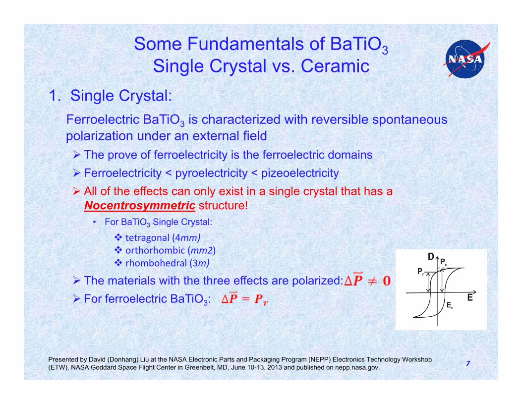
Some Fundamentals of BaTiO3Single Crystal vs. Ceramic
1. Single Crystal:Ferroelectric BaTiO3 is characterized with reversible spontaneous polarization under an external field The prove of ferroelectricity is the ferroelectric domains Ferroelectricity < pyroelectricity < pizeoelectricity All of the effects can only exist in a single crystal that has a
Nocentrosymmetric structure! • For BaTiO3 Single Crystal:
tetragonal (4mm) orthorhombic (mm2) rhombohedral (3m)
The materials with the three effects are polarized: For ferroelectric BaTiO3:
7Presented by David (Donhang) Liu at the NASA Electronic Parts and Packaging Program (NEPP) Electronics Technology Workshop (ETW), NASA Goddard Space Flight Center in Greenbelt, MD, June 10-13, 2013 and published on nepp.nasa.gov.

Some Fundamentals of BaTiO3Single Crystal vs. Ceramic
2. Ceramic:• Ceramic is a polycrystalline material that contains great number of
closed-packed single crystal grains• In a ceramic BaTiO3 structure, although each grain is polarized, the
ceramic posses a centrosymmetric structure and is neither polarized, nor piezoelectric!
• Why?• How?
How to make a BaTiO3 MLCC piezoelectric? Why BaTiO3 thin film can be a DRAM device?
8
When talk about BaTiO3, make sure it is single crystal, or ceramic Grain boundary often determines the unique properties of a ceramic “Structure-Property” relation is the key for performance of a material
Presented by David (Donhang) Liu at the NASA Electronic Parts and Packaging Program (NEPP) Electronics Technology Workshop (ETW), NASA Goddard Space Flight Center in Greenbelt, MD, June 10-13, 2013 and published on nepp.nasa.gov.
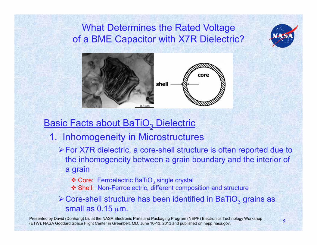
What Determines the Rated Voltageof a BME Capacitor with X7R Dielectric?
Basic Facts about BaTiO3 Dielectric1. Inhomogeneity in MicrostructuresFor X7R dielectric, a core-shell structure is often reported due to
the inhomogeneity between a grain boundary and the interior of a grain Core: Ferroelectric BaTiO3 single crystal Shell: Non-Ferroelectric, different composition and structure
Core-shell structure has been identified in BaTiO3 grains as small as 0.15 m.
9Presented by David (Donhang) Liu at the NASA Electronic Parts and Packaging Program (NEPP) Electronics Technology Workshop (ETW), NASA Goddard Space Flight Center in Greenbelt, MD, June 10-13, 2013 and published on nepp.nasa.gov.

What Determines the Rated Voltageof a BME capacitor with X7R Dielectric?
Basic Facts about BaTiO3 Dielectric (Cont’d)2. Inhomogeneity in resistivity Core is relative conductive; shell is highly resistive (holding the high
resistivity for BaTiO3 dielectric) The applied voltage distribution is inhomogeneous Due to the formation of a high insulating layer at the grain boundary,
most of the voltage will be applied on the grain boundary region
10
35oC 85oC 125oC
Presented by David (Donhang) Liu at the NASA Electronic Parts and Packaging Program (NEPP) Electronics Technology Workshop (ETW), NASA Goddard Space Flight Center in Greenbelt, MD, June 10-13, 2013 and published on nepp.nasa.gov.
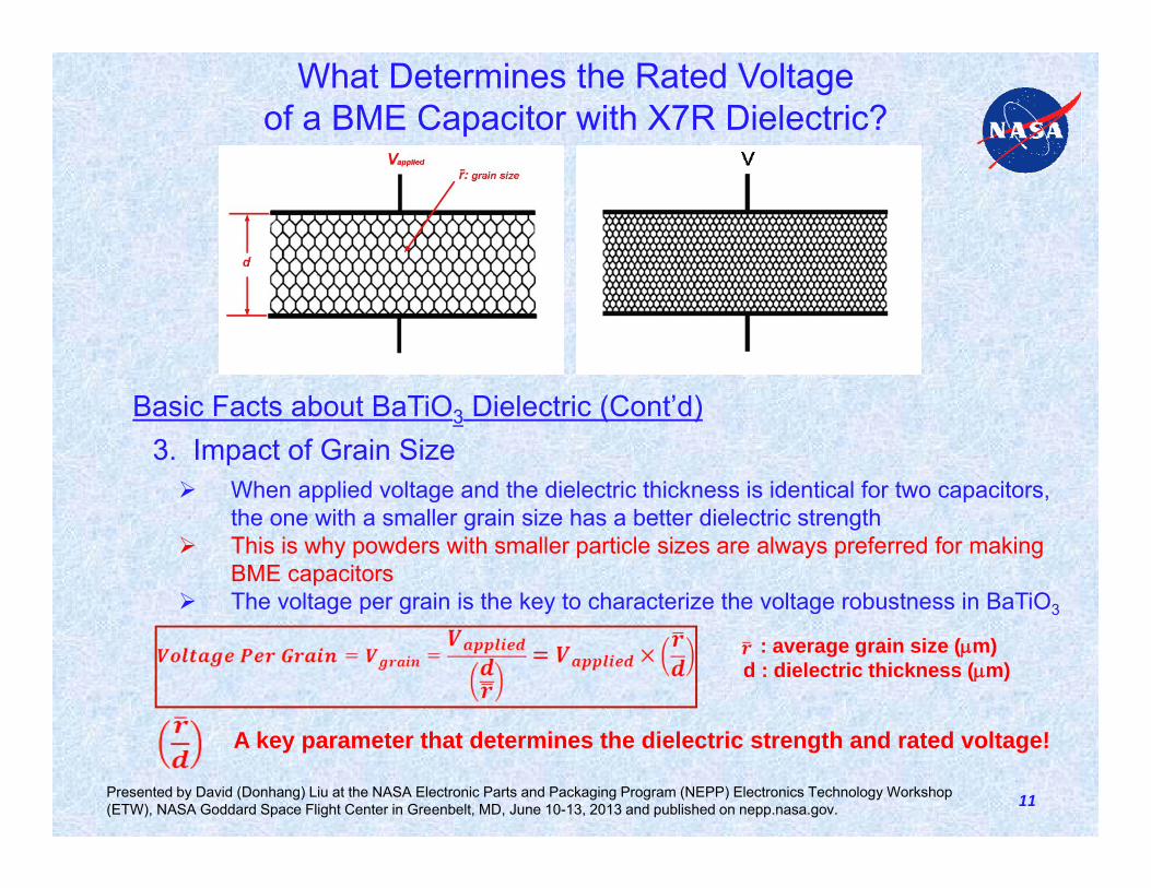
What Determines the Rated Voltageof a BME Capacitor with X7R Dielectric?
Basic Facts about BaTiO3 Dielectric (Cont’d)3. Impact of Grain Size When applied voltage and the dielectric thickness is identical for two capacitors,
the one with a smaller grain size has a better dielectric strength This is why powders with smaller particle sizes are always preferred for making
BME capacitors The voltage per grain is the key to characterize the voltage robustness in BaTiO3
11
: average grain size (m)d : dielectric thickness (m)
A key parameter that determines the dielectric strength and rated voltage!
Presented by David (Donhang) Liu at the NASA Electronic Parts and Packaging Program (NEPP) Electronics Technology Workshop (ETW), NASA Goddard Space Flight Center in Greenbelt, MD, June 10-13, 2013 and published on nepp.nasa.gov.
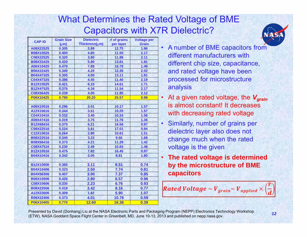
What Determines the Rated Voltage of BME Capacitors with X7R Dielectric?
• A number of BME capacitors from different manufacturers with different chip size, capacitance, and rated voltage have been processed for microstructure analysis
• At a given rated voltage, the Vgrainis almost constant! It decreases with decreasing rated voltage
• Similarly, number of grains per dielectric layer also does not change much when the rated voltage is the given
• The rated voltage is determined by the microstructure of BME capacitors
12
CAP ID Grain Size (m)
Dielectric Thickness(m)
# of grains per layer
Voltage per Grain
A08X22525 0.305 3.89 12.75 1.96B08X10525 0.400 4.60 11.50 2.17C08X22525 0.320 3.80 11.88 2.11B08X33425 0.420 5.80 13.81 1.81A06X10425 0.470 7.89 16.79 1.49B06X22425 0.340 4.20 12.35 2.02B04X47325 0.305 4.00 13.11 1.91C04X47325 0.386 4.40 11.40 2.19B12X10525 0.421 6.15 14.61 1.71B12X47525 0.376 4.34 11.54 2.17C08X56425 0.339 4.00 11.80 2.12P08X10425 0.790 20.20 25.57 0.98
A06X10516 0.296 3.01 10.17 1.57A12X10616 0.344 3.51 10.20 1.57C04X10416 0.332 3.40 10.24 1.56A08X47416 0.319 3.75 11.76 1.36B12X68416 0.375 6.21 16.56 0.97C08X22516 0.224 3.81 17.01 0.94C12X10616 0.264 2.80 10.61 1.51B08X22516 0.340 3.23 9.50 1.68B08X56416 0.373 4.21 11.29 1.42C08X47516 0.230 2.49 10.83 1.48B12X10516 0.475 7.82 16.45 0.97B04X10416 0.342 3.05 8.91 1.80
B12X10606 0.365 3.11 8.51 0.74B04X10406 0.323 2.50 7.74 0.81B04X56306 0.407 3.00 7.37 0.85B06X10506 0.426 2.80 6.57 0.96C08X10606 0.330 2.23 6.76 0.93B08X22506 0.419 3.42 8.16 0.77A12X22606 0.309 1.82 5.90 1.07B06X22406 0.373 4.01 10.76 0.59P06X10405 0.770 12.60 16.36 0.39
Presented by David (Donhang) Liu at the NASA Electronic Parts and Packaging Program (NEPP) Electronics Technology Workshop (ETW), NASA Goddard Space Flight Center in Greenbelt, MD, June 10-13, 2013 and published on nepp.nasa.gov.
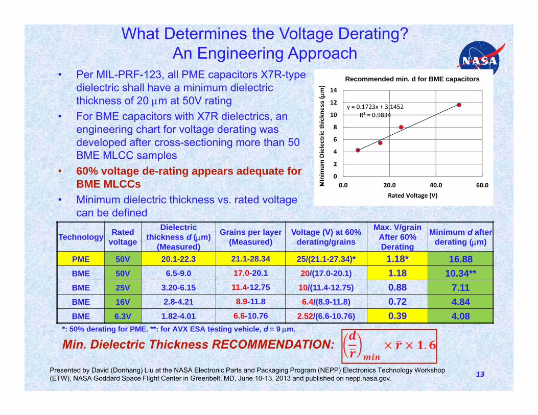
What Determines the Voltage Derating? An Engineering Approach
• Per MIL-PRF-123, all PME capacitors X7R-type dielectric shall have a minimum dielectric thickness of 20 m at 50V rating
• For BME capacitors with X7R dielectrics, an engineering chart for voltage derating was developed after cross-sectioning more than 50 BME MLCC samples
• 60% voltage de-rating appears adequate for BME MLCCs
• Minimum dielectric thickness vs. rated voltage can be defined
13
Technology Rated voltage
Dielectric thickness d (m)
(Measured)
Grains per layer (Measured)
Voltage (V) at 60% derating/grains
Max. V/grainAfter 60% Derating
Minimum d after derating (m)
PME 50V 20.1-22.3 21.1-28.34 25/(21.1-27.34)* 1.18* 16.88BME 50V 6.5-9.0 17.0-20.1 20/(17.0-20.1) 1.18 10.34**BME 25V 3.20-6.15 11.4-12.75 10/(11.4-12.75) 0.88 7.11BME 16V 2.8-4.21 8.9-11.8 6.4/(8.9-11.8) 0.72 4.84BME 6.3V 1.82-4.01 6.6-10.76 2.52/(6.6-10.76) 0.39 4.08
Min. Dielectric Thickness RECOMMENDATION:
y = 0.1723x + 3.1452R² = 0.9834
0
2
4
6
8
10
12
14
0.0 20.0 40.0 60.0MIn
imum
Die
lect
ric th
ickn
ess(m)
Rated Voltage (V)
Recommended min. d for BME capacitors
*: 50% derating for PME. **: for AVX ESA testing vehicle, d = 9 m.
Presented by David (Donhang) Liu at the NASA Electronic Parts and Packaging Program (NEPP) Electronics Technology Workshop (ETW), NASA Goddard Space Flight Center in Greenbelt, MD, June 10-13, 2013 and published on nepp.nasa.gov.
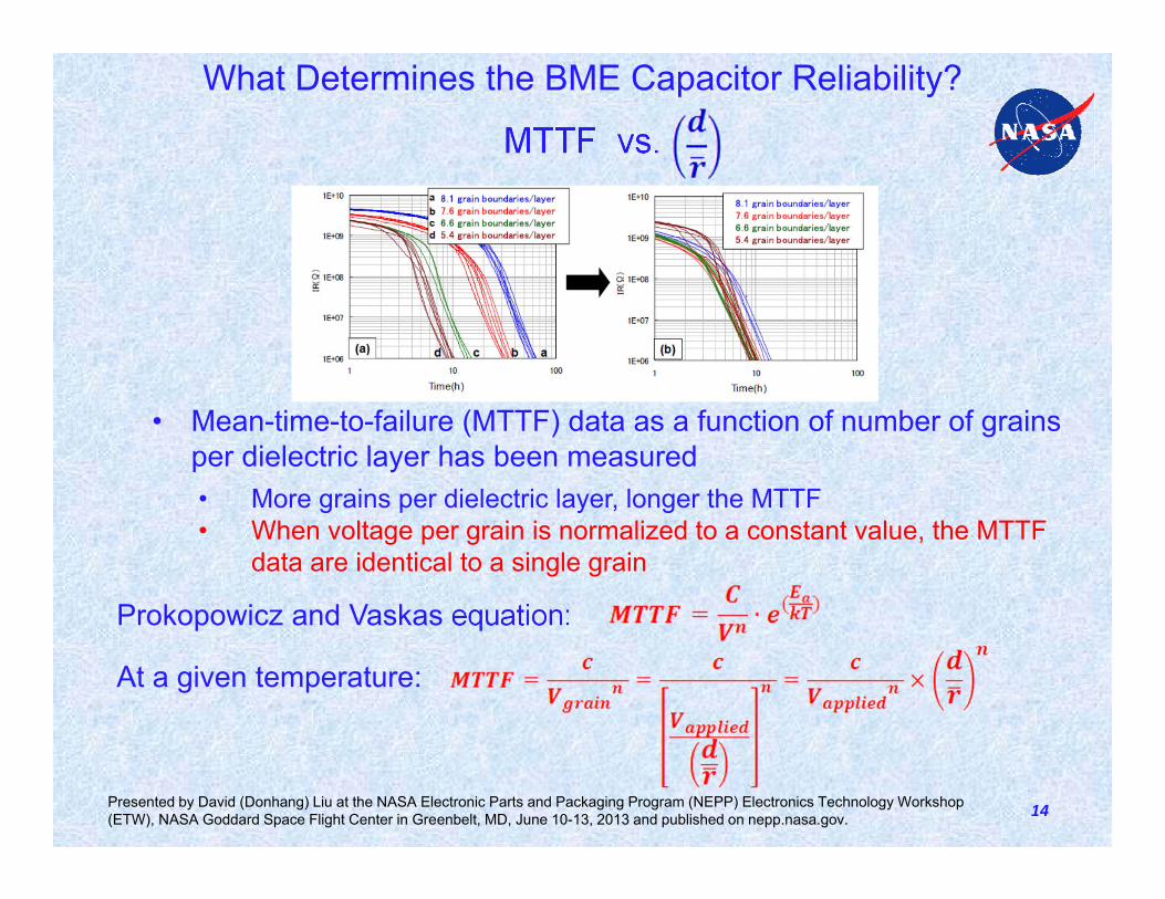
What Determines the BME Capacitor Reliability?
MTTF vs.
• Mean-time-to-failure (MTTF) data as a function of number of grains per dielectric layer has been measured• More grains per dielectric layer, longer the MTTF• When voltage per grain is normalized to a constant value, the MTTF
data are identical to a single grain
14
Prokopowicz and Vaskas equation:
At a given temperature:
Presented by David (Donhang) Liu at the NASA Electronic Parts and Packaging Program (NEPP) Electronics Technology Workshop (ETW), NASA Goddard Space Flight Center in Greenbelt, MD, June 10-13, 2013 and published on nepp.nasa.gov.
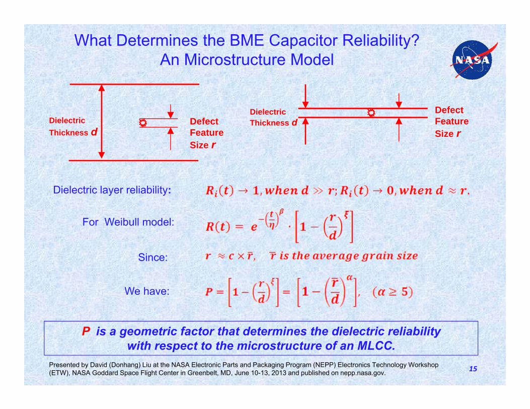
What Determines the BME Capacitor Reliability? An Microstructure Model
15
Dielectric Thickness d
Defect Feature Size r
Dielectric Thickness d
Defect Feature Size r
P is a geometric factor that determines the dielectric reliabilitywith respect to the microstructure of an MLCC.
For Weibull model:
Since:
Dielectric layer reliability:
We have:
Presented by David (Donhang) Liu at the NASA Electronic Parts and Packaging Program (NEPP) Electronics Technology Workshop (ETW), NASA Goddard Space Flight Center in Greenbelt, MD, June 10-13, 2013 and published on nepp.nasa.gov.
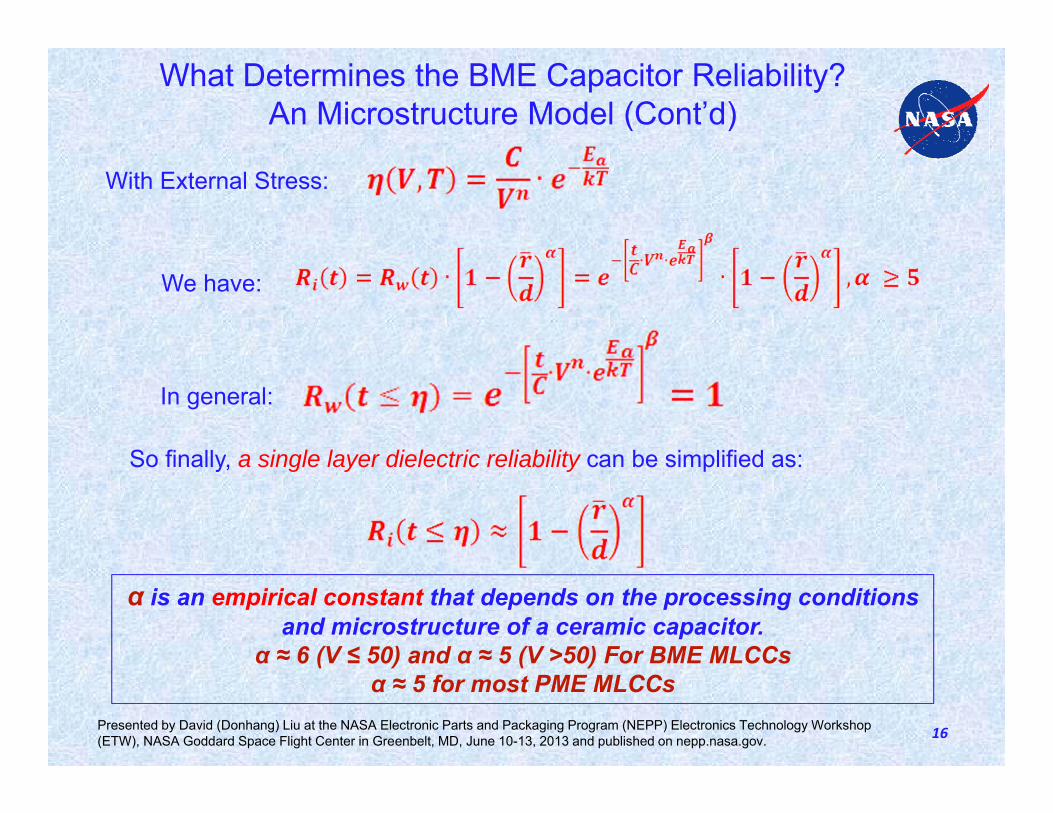
16
α is an empirical constant that depends on the processing conditions and microstructure of a ceramic capacitor.
α ≈ 6 (V ≤ 50) and α ≈ 5 (V >50) For BME MLCCsα ≈ 5 for most PME MLCCs
What Determines the BME Capacitor Reliability? An Microstructure Model (Cont’d)
In general:
With External Stress:
We have:
So finally, a single layer dielectric reliability can be simplified as:
Presented by David (Donhang) Liu at the NASA Electronic Parts and Packaging Program (NEPP) Electronics Technology Workshop (ETW), NASA Goddard Space Flight Center in Greenbelt, MD, June 10-13, 2013 and published on nepp.nasa.gov.
17
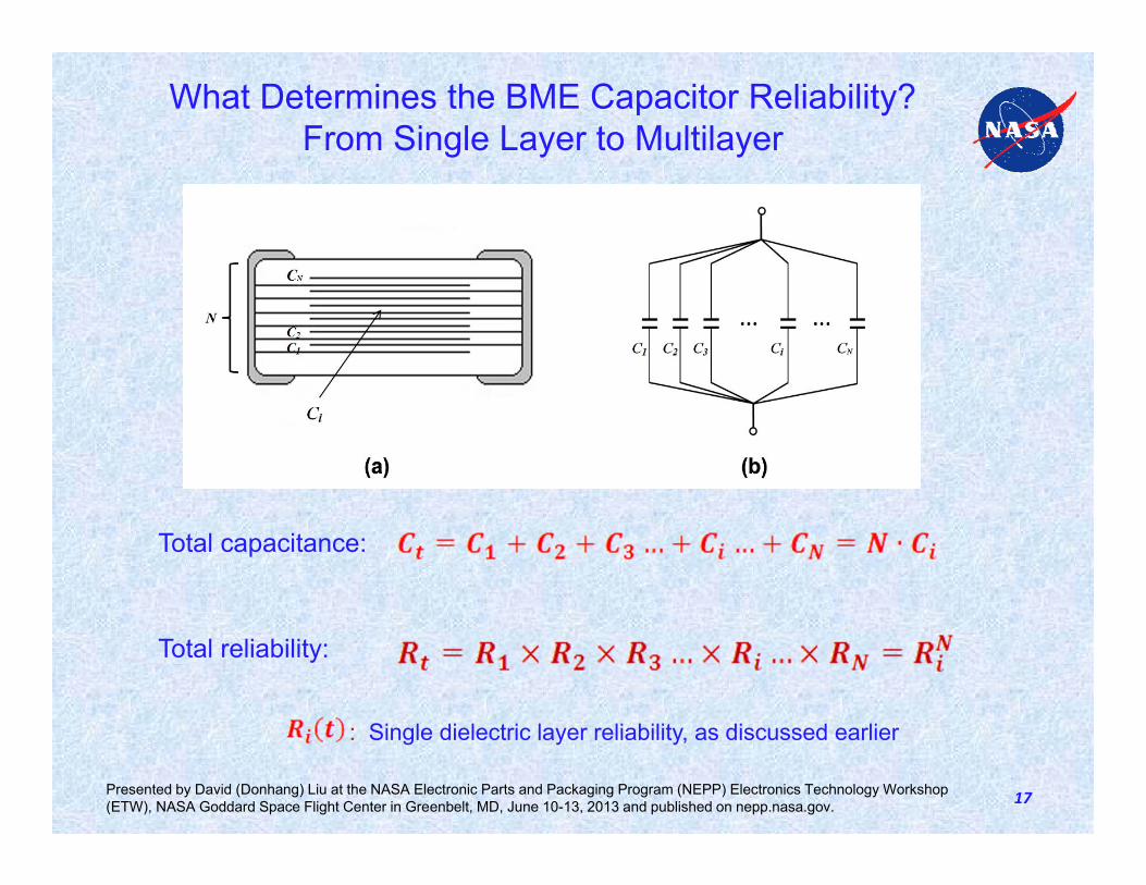
What Determines the BME Capacitor Reliability? From Single Layer to Multilayer
Total capacitance:
Total reliability:
: Single dielectric layer reliability, as discussed earlier
Presented by David (Donhang) Liu at the NASA Electronic Parts and Packaging Program (NEPP) Electronics Technology Workshop (ETW), NASA Goddard Space Flight Center in Greenbelt, MD, June 10-13, 2013 and published on nepp.nasa.gov.
18
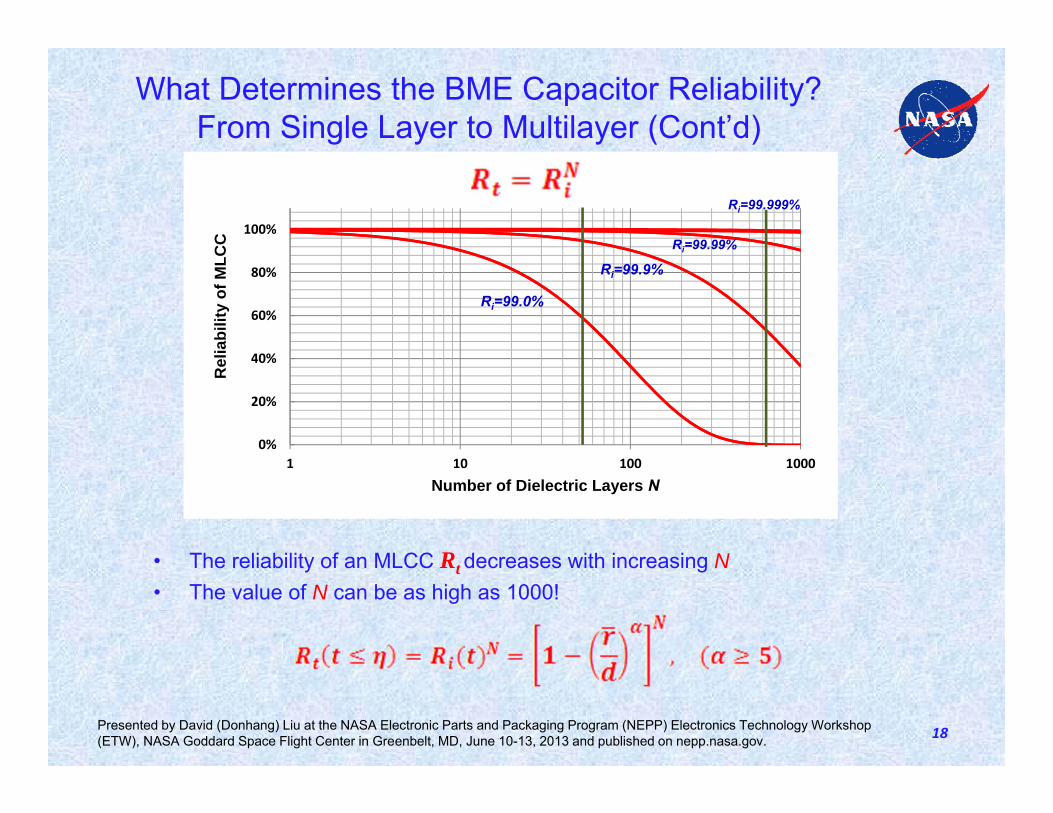
What Determines the BME Capacitor Reliability? From Single Layer to Multilayer (Cont’d)
• The reliability of an MLCC Rt decreases with increasing N• The value of N can be as high as 1000!
0%
20%
40%
60%
80%
100%
1 10 100 1000
Rel
iabi
lity
of M
LCC
Number of Dielectric Layers N
Ri=99.0%
Ri=99.9%Ri=99.99%
Ri=99.999%
Presented by David (Donhang) Liu at the NASA Electronic Parts and Packaging Program (NEPP) Electronics Technology Workshop (ETW), NASA Goddard Space Flight Center in Greenbelt, MD, June 10-13, 2013 and published on nepp.nasa.gov.
19
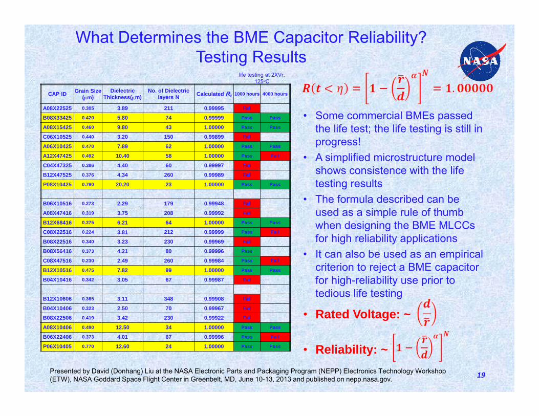
What Determines the BME Capacitor Reliability? Testing Results
• Some commercial BMEs passed the life test; the life testing is still in progress!
• A simplified microstructure model shows consistence with the life testing results
• The formula described can be used as a simple rule of thumb when designing the BME MLCCs for high reliability applications
• It can also be used as an empirical criterion to reject a BME capacitor for high-reliability use prior to tedious life testing
• Rated Voltage: ~
• Reliability: ~
life testing at 2XVr, 125oC
CAP ID Grain Size (m)
Dielectric Thickness(m)
No. of Dielectric layers N Calculated Rt 1000 hours 4000 hours
A08X22525 0.305 3.89 211 0.99995 Fail
B08X33425 0.420 5.80 74 0.99999 Pass Pass
A08X15425 0.460 9.80 43 1.00000 Pass Pass
C06X10525 0.440 3.20 150 0.99899 Fail
A06X10425 0.470 7.89 62 1.00000 Pass Pass
A12X47425 0.492 10.40 58 1.00000 Pass Fail
C04X47325 0.386 4.40 60 0.99997 Fail
B12X47525 0.376 4.34 260 0.99989 Fail
P08X10425 0.790 20.20 23 1.00000 Pass Pass
B06X10516 0.273 2.29 179 0.99948 Fail
A08X47416 0.319 3.75 208 0.99992 Fail
B12X68416 0.375 6.21 64 1.00000 Pass Pass
C08X22516 0.224 3.81 212 0.99999 Pass Fail
B08X22516 0.340 3.23 230 0.99969 Fail
B08X56416 0.373 4.21 80 0.99996 Pass
C08X47516 0.230 2.49 260 0.99984 Pass Fail
B12X10516 0.475 7.82 99 1.00000 Pass Pass
B04X10416 0.342 3.05 67 0.99987 Fail
B12X10606 0.365 3.11 348 0.99908 Fail
B04X10406 0.323 2.50 70 0.99967 Fail
B08X22506 0.419 3.42 230 0.99922 Fail
A08X10406 0.490 12.50 34 1.00000 Pass Pass
B06X22406 0.373 4.01 67 0.99996 Pass Fail
P06X10405 0.770 12.60 24 1.00000 Pass Pass
Presented by David (Donhang) Liu at the NASA Electronic Parts and Packaging Program (NEPP) Electronics Technology Workshop (ETW), NASA Goddard Space Flight Center in Greenbelt, MD, June 10-13, 2013 and published on nepp.nasa.gov.
20
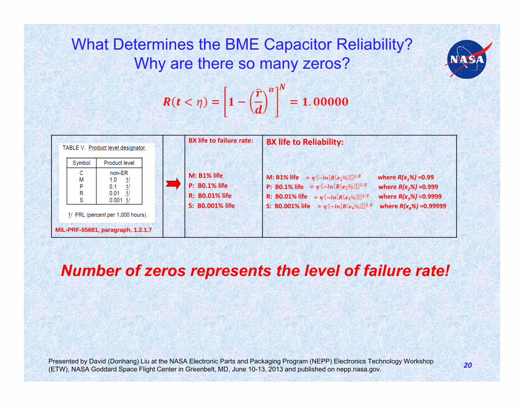
What Determines the BME Capacitor Reliability? Why are there so many zeros?
MIL-PRF-55681, paragraph, 1.2.1.7
BX life to failure rate:
M: B1% lifeP: B0.1% lifeR: B0.01% lifeS: B0.001% life
BX life to Reliability:
M: B1% life where R(x1%) =0.99P: B0.1% life where R(x2%) =0.999R: B0.01% life where R(x3%) =0.9999S: B0.001% life where R(x4%) =0.99999
Number of zeros represents the level of failure rate!
Presented by David (Donhang) Liu at the NASA Electronic Parts and Packaging Program (NEPP) Electronics Technology Workshop (ETW), NASA Goddard Space Flight Center in Greenbelt, MD, June 10-13, 2013 and published on nepp.nasa.gov.
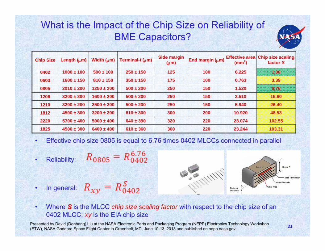
Chip Size Length (m) Width (m) Terminal-t (m) Side margin (m) End margin (m) Effective area
(mm2)Chip size scaling
factor S
0402 1000 ± 100 500 ± 100 250 ± 150 125 100 0.225 1.00
0603 1600 ± 150 810 ± 150 350 ± 150 175 100 0.763 3.39
0805 2010 ± 200 1250 ± 200 500 ± 200 250 150 1.520 6.76
1206 3200 ± 200 1600 ± 200 500 ± 200 250 150 3.510 15.60
1210 3200 ± 200 2500 ± 200 500 ± 200 250 150 5.940 26.40
1812 4500 ± 300 3200 ± 200 610 ± 300 300 200 10.920 48.53
2220 5700 ± 400 5000 ± 400 640 ± 390 320 220 23.074 102.55
1825 4500 ± 300 6400 ± 400 610 ± 360 300 220 23.244 103.31
21
What is the Impact of the Chip Size on Reliability of BME Capacitors?
• Effective chip size 0805 is equal to 6.76 times 0402 MLCCs connected in parallel
• Reliability:
• In general:
• Where S is the MLCC chip size scaling factor with respect to the chip size of an 0402 MLCC; xy is the EIA chip size
Presented by David (Donhang) Liu at the NASA Electronic Parts and Packaging Program (NEPP) Electronics Technology Workshop (ETW), NASA Goddard Space Flight Center in Greenbelt, MD, June 10-13, 2013 and published on nepp.nasa.gov.
22
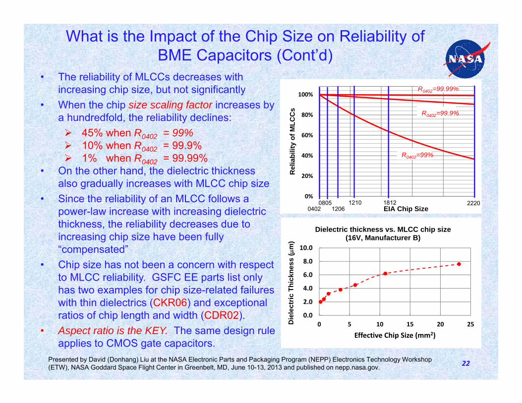
What is the Impact of the Chip Size on Reliability of BME Capacitors (Cont’d)
• The reliability of MLCCs decreases with increasing chip size, but not significantly
• When the chip size scaling factor increases by a hundredfold, the reliability declines: 45% when R0402 = 99% 10% when R0402 = 99.9% 1% when R0402 = 99.99%
• On the other hand, the dielectric thickness also gradually increases with MLCC chip size
• Since the reliability of an MLCC follows a power-law increase with increasing dielectric thickness, the reliability decreases due to increasing chip size have been fully “compensated”
• Chip size has not been a concern with respect to MLCC reliability. GSFC EE parts list only has two examples for chip size-related failures with thin dielectrics (CKR06) and exceptional ratios of chip length and width (CDR02).
• Aspect ratio is the KEY. The same design rule applies to CMOS gate capacitors.
0.0
2.0
4.0
6.0
8.0
10.0
0 5 10 15 20 25Die
lect
ric T
hick
ness
(m
)
Effective Chip Size (mm2)
Dielectric thickness vs. MLCC chip size(16V, Manufacturer B)
0%
20%
40%
60%
80%
100%
Rel
iabi
lity
of M
LCC
s
EIA Chip Size04020805
12061210 1812 2220
R0402=99%
R0402=99.9%
R0402=99.99%
Presented by David (Donhang) Liu at the NASA Electronic Parts and Packaging Program (NEPP) Electronics Technology Workshop (ETW), NASA Goddard Space Flight Center in Greenbelt, MD, June 10-13, 2013 and published on nepp.nasa.gov.
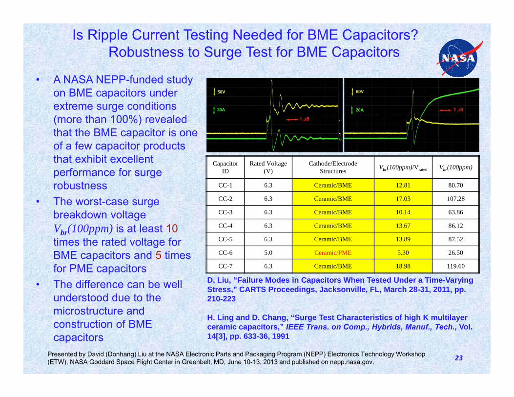
Is Ripple Current Testing Needed for BME Capacitors?Robustness to Surge Test for BME Capacitors
• A NASA NEPP-funded study on BME capacitors under extreme surge conditions (more than 100%) revealed that the BME capacitor is one of a few capacitor products that exhibit excellent performance for surge robustness
• The worst-case surge breakdown voltage Vbr(100ppm) is at least 10times the rated voltage for BME capacitors and 5 times for PME capacitors
• The difference can be well understood due to the microstructure and construction of BME capacitors
23
Capacitor ID
Rated Voltage (V)
Cathode/Electrode Structures Vbr(100ppm)/Vrated Vbr(100ppm)
CC-1 6.3 Ceramic/BME 12.81 80.70
CC-2 6.3 Ceramic/BME 17.03 107.28
CC-3 6.3 Ceramic/BME 10.14 63.86
CC-4 6.3 Ceramic/BME 13.67 86.12
CC-5 6.3 Ceramic/BME 13.89 87.52
CC-6 5.0 Ceramic/PME 5.30 26.50
CC-7 6.3 Ceramic/BME 18.98 119.60
D. Liu, “Failure Modes in Capacitors When Tested Under a Time-Varying Stress,” CARTS Proceedings, Jacksonville, FL, March 28-31, 2011, pp. 210-223
H. Ling and D. Chang, “Surge Test Characteristics of high K multilayer ceramic capacitors,” IEEE Trans. on Comp., Hybrids, Manuf., Tech., Vol. 14[3], pp. 633-36, 1991
Presented by David (Donhang) Liu at the NASA Electronic Parts and Packaging Program (NEPP) Electronics Technology Workshop (ETW), NASA Goddard Space Flight Center in Greenbelt, MD, June 10-13, 2013 and published on nepp.nasa.gov.
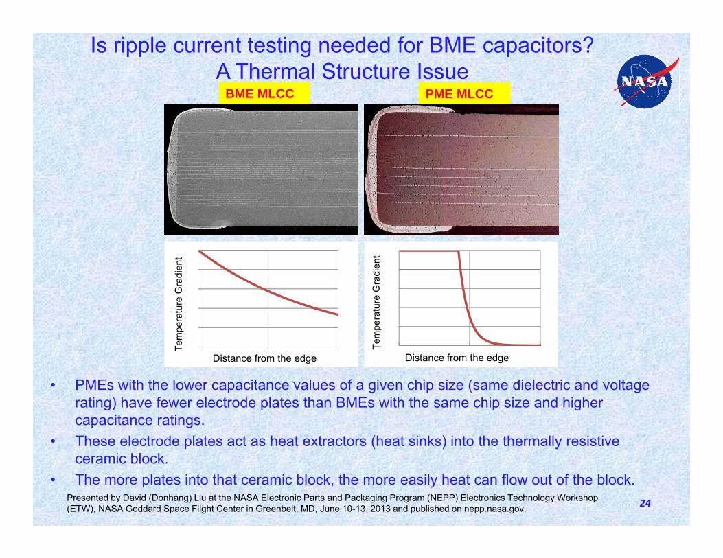
Is ripple current testing needed for BME capacitors?A Thermal Structure Issue
24
• PMEs with the lower capacitance values of a given chip size (same dielectric and voltage rating) have fewer electrode plates than BMEs with the same chip size and higher capacitance ratings.
• These electrode plates act as heat extractors (heat sinks) into the thermally resistive ceramic block.
• The more plates into that ceramic block, the more easily heat can flow out of the block.
BME MLCC PME MLCC
0
20
40
60
80
100
0 50 100
Tem
pera
ture
Gra
dien
t
Distance from the edge0
20
40
60
80
100
0 50 100Te
mpe
ratu
re G
radi
ent
Distance from the edge
Presented by David (Donhang) Liu at the NASA Electronic Parts and Packaging Program (NEPP) Electronics Technology Workshop (ETW), NASA Goddard Space Flight Center in Greenbelt, MD, June 10-13, 2013 and published on nepp.nasa.gov.
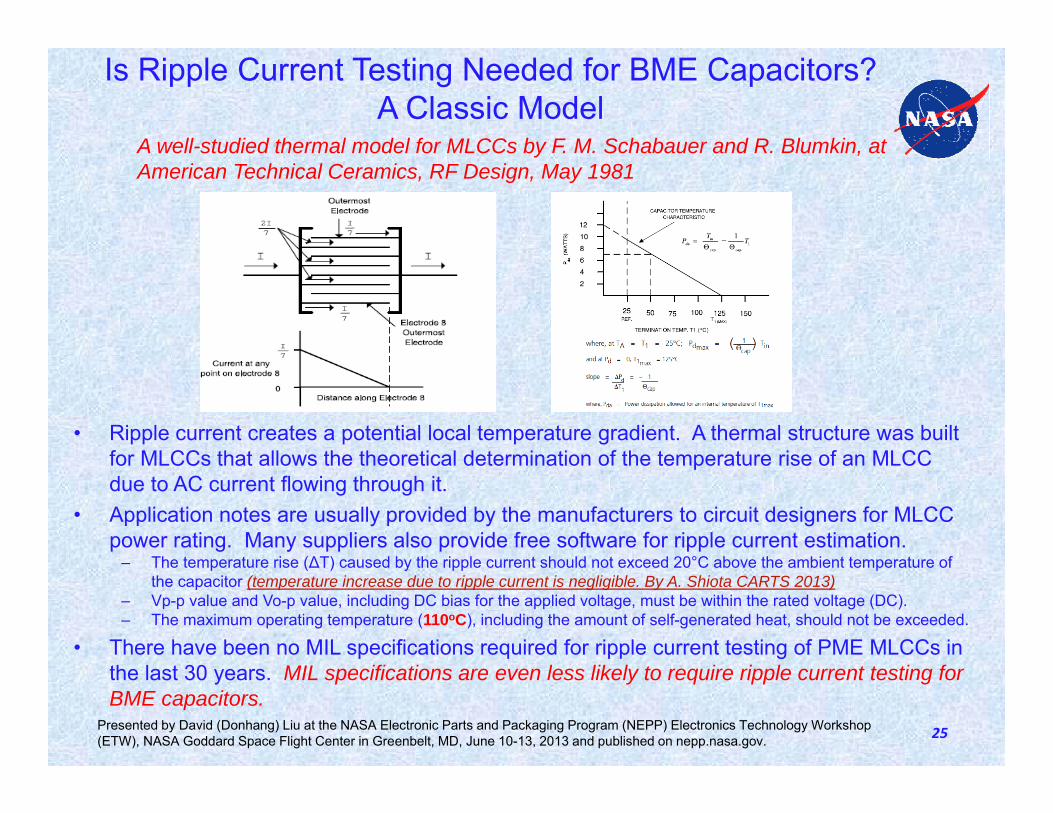
Is Ripple Current Testing Needed for BME Capacitors? A Classic Model
25
• Ripple current creates a potential local temperature gradient. A thermal structure was built for MLCCs that allows the theoretical determination of the temperature rise of an MLCC due to AC current flowing through it.
• Application notes are usually provided by the manufacturers to circuit designers for MLCC power rating. Many suppliers also provide free software for ripple current estimation.
– The temperature rise (∆T) caused by the ripple current should not exceed 20°C above the ambient temperature of the capacitor (temperature increase due to ripple current is negligible. By A. Shiota CARTS 2013)
– Vp-p value and Vo-p value, including DC bias for the applied voltage, must be within the rated voltage (DC).– The maximum operating temperature (110oC), including the amount of self-generated heat, should not be exceeded.
• There have been no MIL specifications required for ripple current testing of PME MLCCs in the last 30 years. MIL specifications are even less likely to require ripple current testing for BME capacitors.
A well-studied thermal model for MLCCs by F. M. Schabauer and R. Blumkin, at American Technical Ceramics, RF Design, May 1981
Presented by David (Donhang) Liu at the NASA Electronic Parts and Packaging Program (NEPP) Electronics Technology Workshop (ETW), NASA Goddard Space Flight Center in Greenbelt, MD, June 10-13, 2013 and published on nepp.nasa.gov.
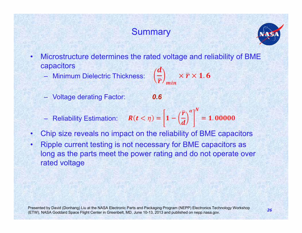
Summary
• Microstructure determines the rated voltage and reliability of BME capacitors– Minimum Dielectric Thickness:
– Voltage derating Factor: 0.6
– Reliability Estimation:
• Chip size reveals no impact on the reliability of BME capacitors• Ripple current testing is not necessary for BME capacitors as
long as the parts meet the power rating and do not operate over rated voltage
26Presented by David (Donhang) Liu at the NASA Electronic Parts and Packaging Program (NEPP) Electronics Technology Workshop (ETW), NASA Goddard Space Flight Center in Greenbelt, MD, June 10-13, 2013 and published on nepp.nasa.gov.