hsp: a surface-potential- based compact model of...
TRANSCRIPT

© CEA. All rights reserved
| PAGE 1
HSP: A Surface-Potential-
Based Compact Model
of AlGaN/GaN HEMTs
Power Transistors
Patrick Martin and Rereao Hahe
CEA, Leti, Silicon Components Division,
Simulation and Modeling Laboratory,
Minatec Campus, Grenoble, France.
10th MOS-AK/GSA ESSDERC/ESSCIRC Workshop Bordeaux, France - September 21, 2012. | PAGE 1

HSP: A Surface-Potential-Based Compact Model of AlGaN/GaN HEMTs Power Transistors, MOS-AK Bordeaux, Sept. 21, 2012
© CEA. All rights reserved
| 2
Summary
Motivation
Existing models for GaN power transistors, need for a more physical model
GaN material specificity for power transistors
HSP model flow
AlGaN/GaN energy band diagram and electrostatics
Analytical EF calculation, a tedious mathematical!
Comparison of Numerical & Analytical EF calculation
Velocity saturation and mobility model
Self-heating modeling
Doping of AlGaN by ion implantation
Calculation of drain current
Intrinsic charge model
HSP model parameter list
Results: parameter extraction, DC, self-heating
Summary and conclusions

HSP: A Surface-Potential-Based Compact Model of AlGaN/GaN HEMTs Power Transistors, MOS-AK Bordeaux, Sept. 21, 2012
© CEA. All rights reserved
| 3
Motivation
Low cost, high performance devices used in energy
conversion electronic circuits
Applications: mainly switching applications, not analogue/RF
amplification
Low cost if substrate diameter greater than 4“ - 100 mm (SiC)
High performance: high switching speed
GaN is a promising candidate for power applications
(1200 V - 300 A, power ~ kW, high operating temperature
about 250 °C)
High breakdown field > 3 MV/cm
High mobility in HEMT (High Electron Mobility Transistor)
High electron saturation velocity: 1.2 107 cm/s
Wide bandgap semiconductor
AlGaN/GaN HEMTs
HSP: A Surface-Potential-Based Compact Model of AlGaN/GaN HEMTs Power Transistors, MOS-AK Bordeaux, Sept. 21, 2012
© CEA. All rights reserved
| 4
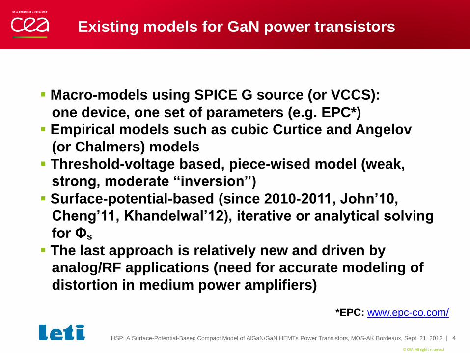
Existing models for GaN power transistors
Macro-models using SPICE G source (or VCCS):
one device, one set of parameters (e.g. EPC*)
Empirical models such as cubic Curtice and Angelov
(or Chalmers) models
Threshold-voltage based, piece-wised model (weak,
strong, moderate “inversion”)
Surface-potential-based (since 2010-2011, John’10,
Cheng’11, Khandelwal’12), iterative or analytical solving
for Φs
The last approach is relatively new and driven by
analog/RF applications (need for accurate modeling of
distortion in medium power amplifiers)
*EPC: www.epc-co.com/

HSP: A Surface-Potential-Based Compact Model of AlGaN/GaN HEMTs Power Transistors, MOS-AK Bordeaux, Sept. 21, 2012
© CEA. All rights reserved
| 5
Need for a more physical model
A HEMT transistor is not a MESFET or a MOSFET
(III-V compounds, inversion charge, mobility, …)
Many materials properties are Al-content and temperature
dependent (Eg, σ, …)
Heterostructures growth technique has a strong impact
on electrical properties
HP devices will work at high temperature
Self-heating effects will be very important
Refractory compounds: donors are not fully ionized at RT,
the ratio Nd+/Nd is temperature-dependent

HSP: A Surface-Potential-Based Compact Model of AlGaN/GaN HEMTs Power Transistors, MOS-AK Bordeaux, Sept. 21, 2012
© CEA. All rights reserved
| 6
AlGaN/GaN HEMT schematic structure
Silicon substrate
Schottky Gate
Gate length (L)
So
urc
e D
rain
Buffer
Undoped GaN 2D electron gas
n-doped AlxGa1-xN layer (thickness dd)
Undoped AlxGa1-xN (thickness di)
ILD
aSi=0.54 nm
aGaN=0.32/0.51 nm
(a/c axis)
Important Δa/a
KSi=150 W/m.K
KGaN=130
KSiC=320
Thermal conductivity:
Lattice
constants:

HSP: A Surface-Potential-Based Compact Model of AlGaN/GaN HEMTs Power Transistors, MOS-AK Bordeaux, Sept. 21, 2012
© CEA. All rights reserved
| 7
GaN material specificity for power transistors
Large conduction band discontinuity ΔEc between
AlGaN and GaN: 2-Dimensional Electron Gas (2DEG)
ΔEc alone is not sufficient to explain very high charge
sheet density of the 2DEG, in excess of 1013 cm-2, even
without intentional doping
Additional effect: polarization-induced sheet carrier
concentration leading to a strong confinement of 2DEG 1 - Spontaneous polarization (SP) due to anion/cation in
lattice, resulting electrical field=3 MV/cm
2 - Piezoelectric polarization (PZ) proportional to strain:
Δa(x) = a(AlxGa1-xN) - a(GaN), electrical field=2 MV/cm
Drawback: Normally-on transistors (depletion mode)
Work in progress for normally-off HEMTS for safety
reasons
Only N-HEMTs

HSP: A Surface-Potential-Based Compact Model of AlGaN/GaN HEMTs Power Transistors, MOS-AK Bordeaux, Sept. 21, 2012
© CEA. All rights reserved
| 8
Contributions to the offset voltage
Total polarization σ (spontaneous + piezoelectric)
is the main contribution to the offset voltage Voff
MOCVD: Ga face, MBE: N-face
Typical xAl: 0.15-0.5
Donors: Silicon Nd=2 1018 cm-3
From Ambacher’99
Wurtzite= hexagonal form
σ positive σ negative
id
NGaAlNGaAl
ddcBoff dd
qdNqEV
xxxx
112
2

HSP: A Surface-Potential-Based Compact Model of AlGaN/GaN HEMTs Power Transistors, MOS-AK Bordeaux, Sept. 21, 2012
© CEA. All rights reserved
| 9
A Surface-Potential-Based Compact Model of AlGaN/GaN
HEMTs Power Transistors: HSP model flow
Circuit simulation
using ADS
(Agilent)
Verilog-A code
implementation
Parameter
extraction +
literature data
VBA and Matlab
code
development
Schottky gate
current (Ig)
HSP compact model flow
Parameters
Polarization
effects
(SP, PZ)
Temperature
modeling
Incomplete
donor ioniz.
DIBL Effect
Voff
Electrostatics
Φss, Φsd,
Φ, Φsm
Mobility
Velocity
Saturation
Drain current
(Id)
Self-heating
Access
resistances
Parasitic cap.
Charge
partitioning
(Qs/Qd)
2DEG charge
(Qi)
Channel
Length Mod.

HSP: A Surface-Potential-Based Compact Model of AlGaN/GaN HEMTs Power Transistors, MOS-AK Bordeaux, Sept. 21, 2012
© CEA. All rights reserved
| 10
AlGaN/GaN energy band diagram and
electrostatics
Assumptions:
Triangular potential well
Only the first quantum state, E0, is
considered, E1 is neglected
Self-consistent solving of Schrödinger’s
and Poisson’s equations
2DEG sheet carrier concentration ns:
2*
32
00
0
/4
exp1
hmD
nCE
qkT
EELnkTDn
s
Fs
Foffg
AlGaNs EVV
dqn
id
AlGaNAlGaN
ddcBoff dd
qdNqEV
2
2
Numerical resolution for EF

HSP: A Surface-Potential-Based Compact Model of AlGaN/GaN HEMTs Power Transistors, MOS-AK Bordeaux, Sept. 21, 2012
© CEA. All rights reserved
| 11
Analytical EF calculation
Analytical determination of EF is done in two steps:
EF = η + ω
1 - Approximate solution (η) for two asymptotic cases:
(a) for high ns and (b) for low ns
2 - Small refinement (ω), important for medium ns
Refinement is done several times (5-10) to ensure good accuracy
for medium ns
Surface-Potential (Φs) calculation: Φs = EF + Vchannel
At source: Φss = EF + Vs, at drain: Φsd = EF + Vd

HSP: A Surface-Potential-Based Compact Model of AlGaN/GaN HEMTs Power Transistors, MOS-AK Bordeaux, Sept. 21, 2012
© CEA. All rights reserved
| 12
A tedious mathematical development around EF
analytical calculation!
We obtain different analytical
expressions than Cheng’11:
“A Surface-Based Compact Model
for AlGaN/GaN MODFETs”
Our expressions are valid for very
high Vds (1kV)
HSP: A Surface-Potential-Based Compact Model of AlGaN/GaN HEMTs Power Transistors, MOS-AK Bordeaux, Sept. 21, 2012
© CEA. All rights reserved
| 13
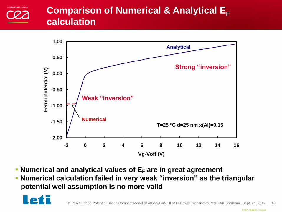
Comparison of Numerical & Analytical EF
calculation
Numerical and analytical values of EF are in great agreement
Numerical calculation failed in very weak “inversion” as the triangular
potential well assumption is no more valid
Weak “inversion”
Strong “inversion”
-2.00
-1.50
-1.00
-0.50
0.00
0.50
1.00
-2 0 2 4 6 8 10 12 14 16
Vg-Voff (V)
Ferm
i p
ote
nti
al
(V)
T=25 °C d=25 nm x(Al)=0.15
Analytical
Numerical

HSP: A Surface-Potential-Based Compact Model of AlGaN/GaN HEMTs Power Transistors, MOS-AK Bordeaux, Sept. 21, 2012
© CEA. All rights reserved
| 14
Velocity saturation and mobility model
Electron drift velocity and negative
differential mobility in III-V semiconductors
Much more simpler mobility model chosen
in HSP:
321
2
0
,,,,
)(
nnnEvPwith
TcTbaPTP
csat
3
1
2
0
1
.
n
c
L
c
L
n
c
LsatL
Ldrift
E
En
E
E
E
EvE
Ev
1
11
1
for
E
E
EE
E
E
E
E
vEv
c
L
L
TLF
c
L
c
L
satLdrift
2
0
1 TT
TLFEE
E
d
VVgE
smoff
AlGaNTGaN
..
ETransverse
ELateral
From Gauss theorem at AlGaN/GaN interface
Schwierz's model - wurtzite GaN
0.0E+00
5.0E+06
1.0E+07
1.5E+07
2.0E+07
2.5E+07
3.0E+07
0E+00 1E+05 2E+05 3E+05 4E+05 5E+05
Electrical field (V/cm)
Dri
ft v
elo
cit
y (
cm
/s)
300K
450 K
600 K
Velocity in bulk wurtzite (hexagonal) GaN

HSP: A Surface-Potential-Based Compact Model of AlGaN/GaN HEMTs Power Transistors, MOS-AK Bordeaux, Sept. 21, 2012
© CEA. All rights reserved
| 15
Self-Heating Effect (SHE) modeling
Thermal conductivity
3 SHE models (SHEMOD)
0 - No SHE
1 - Constant Rth, no heat dissipation through substrate
2 - With heat diffusion through substrate (thickness tsub) and
backside held at constant temperature T0 (Canfield’90)
Iterative calculation of drain current (SHEMOD=2)
KEX
ref
refT
TTT
)(
GaAs: KEX=-1.25 Si: KEX=-1.3 GaN: KEX=-1.4 SiC: KEX=-1.5
4
0
4
0
0
41
411
P
P
P
P
TT
diss
diss
L
8
)(TP
sub
000
tLn
TW
T, Par(T), Id, Pdiss T=T0 + ΔT
α ≤ 1: effective transistor length
where heat dissipation occurs
(Royet’00)
Id’
If ΔId/Id < 10-6 exit loop

HSP: A Surface-Potential-Based Compact Model of AlGaN/GaN HEMTs Power Transistors, MOS-AK Bordeaux, Sept. 21, 2012
© CEA. All rights reserved
| 16
SHE: example of convergence
36.73
36.73
36.73
36.73
36.73
36.74
36.74
36.74
0 5 10
Iteration number
Delt
aT
(K
)
1E-07
1E-06
1E-05
1E-04
1E-03
1E-02
Rela
tive e
rror
OP1: 5 V, 35 mA, 0.17 W OP2: 25 V, 23 mA, 0.58 W
SHE_MOD=2
α=1
κ=150 W.m-1.K-1 (Si)
KEX=-1.3
Tsub=400 µm
T0=25 °C
W=75 µm
L=1 µm
Vg=1 V
Temp=25 °C
OP1
OP2
158.90
159.00
159.10
159.20
159.30
159.40
159.50
159.60
159.70
159.80
159.90
0 5 10 15 20
Iteration number
Delt
aT
(K
)
1E-07
1E-06
1E-05
1E-04
1E-03
1E-02
Rela
tive e
rror

HSP: A Surface-Potential-Based Compact Model of AlGaN/GaN HEMTs Power Transistors, MOS-AK Bordeaux, Sept. 21, 2012
© CEA. All rights reserved
| 17
Doping of AlGaN by Silicon ion implantation
Si substitutes for Ga in the lattice and acts as a donor
Ionization of deep levels is incomplete at RT in refractory
materials
Two activation energies: ΔED1=12-17 meV, ΔED2=32-77 meV
(Götz’96, GaN MOCVD films)
Activation efficiency is function of implant temperature
(Irokawa 2006): ~ 50 % at RT implantation
Charge neutrality equation to be solved:
n: Effective donor concentration
i: Index of donor
g: Degeneracy (g=2)
NC: Density of states in CB
ND: Donor concentration
ΔED: Donor activation energy
NA: Conc. of compensing acceptors
A
n
i Di
C
i
Di N
Tk
E
TN
Tng
NTn
1
exp1

HSP: A Surface-Potential-Based Compact Model of AlGaN/GaN HEMTs Power Transistors, MOS-AK Bordeaux, Sept. 21, 2012
© CEA. All rights reserved
| 18
Silicon donors in GaN
Charge neutrality equation solved by the bisection method
ΔED1=15 meV, ΔED2=37 meV (Götz’96, GaN MOCVD films)
ND1=1.1 1017 cm-3, ND2=3.9 1016 cm-3, NA=0, g1=g2=2, NC=4.3 1014 T1.5 cm-3 K-1.5
Three options in HSP (NDMOD):
0: No partial ionization
1: Partial ionization only during temperature modeling
2: Partial ionization during temperature modeling and self-heating
1E+16
1E+17
1E+18
0 100 200 300 400 500 600 700 800 900 1000
Temperature (K)
ND
eff
(c
m-3
)
1
10
100N
um
be
r of ite
ratio
ns
Bisection method, ND=1.49 E17 cm-3
NDeff / ND=80 % at RT
(activation efficiency=100 %)
Ion implantation of Si in AlGaN:
activation efficiency ≤ 50 %
depending on implant
temperature (Irokawa’06)
HSP: A Surface-Potential-Based Compact Model of AlGaN/GaN HEMTs Power Transistors, MOS-AK Bordeaux, Sept. 21, 2012
© CEA. All rights reserved
| 19
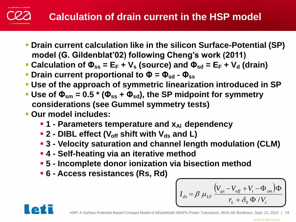
Calculation of drain current in the HSP model
Drain current calculation like in the silicon Surface-Potential (SP)
model (G. Gildenblat’02) following Cheng’s work (2011)
Calculation of Φss = EF + Vs (source) and Φsd = EF + Vd (drain)
Drain current proportional to Φ = Φsd - Φss
Use of the approach of symmetric linearization introduced in SP
Use of Φsm = 0.5 * (Φss + Φsd), the SP midpoint for symmetry
considerations (see Gummel symmetry tests)
Our model includes:
1 - Parameters temperature and xAl dependency
2 - DIBL effect (Voff shift with Vds and L)
3 - Velocity saturation and channel length modulation (CLM)
4 - Self-heating via an iterative method
5 - Incomplete donor ionization via bisection method
6 - Access resistances (Rs, Rd)
cL
smtoffgs
LFdsVr
VVVI
/0

HSP: A Surface-Potential-Based Compact Model of AlGaN/GaN HEMTs Power Transistors, MOS-AK Bordeaux, Sept. 21, 2012
© CEA. All rights reserved
| 20
HSP intrinsic charge model
Importance of charge conservation in circuit simulation
Calculation of Qg
Source and drain charges evaluated using the Ward-
Dutton partitioning scheme
If needed, capacitances will be calculated as derivatives
of the terminal charges: Cij=-dQi/dVj (i≠j), Cii=dQi/dVi (i=j)
9 transcapacitances, 6 are independent due to charge
conservation: Qg + Qs + Qd = 0
HSP: A Surface-Potential-Based Compact Model of AlGaN/GaN HEMTs Power Transistors, MOS-AK Bordeaux, Sept. 21, 2012
© CEA. All rights reserved
| 21
HSP model parameter list (1/2)
Setup parameters:
DATAMOD AlGaN material data
(Ambacher: 0, Yu: 1)
VOFFMOD Set (0) or calculated (1) offset voltage
VOFF Offset voltage
HEMT parameters:
DD N-doped AlGaN layer thickness
DI Undoped AlGaN layer thickness
XAL Al content in AlxGa1-xN
AlGaN doping:
NDMOD Donor partial ionization (0-1-2)
ND Donor concentration (NDMOD=0)
G1 Degeneracy of the 1st donor level
G2 Degeneracy of the 2nd donor level
ED1 1st donor energy level
ED2 2nd donor energy level
ND1 1st donor concentration
ND2 2nd donor concentration
NA Acceptor compensing concentration
AEFF Ion implantation activation efficiency
Geometrical parameters:
L Gate length
W Gate width
DL Gate length offset
DW Gate width offset
Mobility:
MU0 Low field mobility
P1 1st mobility attenuation parameter
P2 2nd mobility attenuation parameter
Velocity Saturation & CLM:
EC Critical electrical field
UA VS parameter
PVS VS parameter
DIBL effect:
DIBL1 DIBL 1st parameter (Vds)
DIBL2 DIBL 2nd parameter (Length)

HSP: A Surface-Potential-Based Compact Model of AlGaN/GaN HEMTs Power Transistors, MOS-AK Bordeaux, Sept. 21, 2012
© CEA. All rights reserved
| 22
HSP model parameter list (2/2)
Self-heating effect:
SHEMOD Self-heating mode (0-1-2-3)
RTH Thermal resistance (SHEMOD=1)
REX Thermal resistance temp. coeff.
CTH Thermal capacitance
TSUB Substrate thickness (SHEMOD=2-3)
ALPHA Fraction of channel length for power
dissipation (SHEMOD=3)
KAPPA Substrate thermal conductivity
KEX Thermal conductivity temp. coeff.
Access resistances:
RS Source resistance
RD Drain resistance
Temperature effects:
TNOM Nominal temperature
TCV VOFF temp. coeff.
MUEX Mobility temp. coeff.
ECEX EC temp. coeff.
TR1 Resistance 1st temp. coeff.
TR2 Resistance 2nd temp. coeff.
Overlap & fringing capacitance:
COV Overlap cap.

HSP: A Surface-Potential-Based Compact Model of AlGaN/GaN HEMTs Power Transistors, MOS-AK Bordeaux, Sept. 21, 2012
© CEA. All rights reserved
| 23
Results: Gummel symmetry tests (GST)
The drain current Id an odd function of Vx. Consequently, all odd order derivatives of
Id(Vx) with respect to Vx should be continuous at Vx=0, and all even order derivatives
should be equal to zero at Vx=0
HSP Gummel symmetry test Vd=Vx, Vs=-Vx
-200
-150
-100
-50
0
50
100
150
200
-1.0 -0.5 0.0 0.5 1.0
Vx (V)
d4Id
s/d
Vx4
Vg=-3 V Vg=-2 V Vg=-1 V Vg=0 V
HSP Gummel symmetry test Vd=Vx, Vs=-Vx
-0.5
-0.4
-0.3
-0.2
-0.1
0.0
0.1
0.2
0.3
0.4
0.5
-1.0 -0.5 0.0 0.5 1.0
Vx (V)
Ids
Vg=-3 V Vg=-2 V Vg=-1 V Vg=0 V
HSP Gummel symmetry test Vd=Vx, Vs=-Vx
-0.5
-0.4
-0.3
-0.2
-0.1
0.0
0.1
0.2
0.3
0.4
0.5
-1.0 -0.5 0.0 0.5 1.0
Vx (V)
d2Id
s/d
Vx2
Vg=-3 V Vg=-2 V Vg=-1 V Vg=0 V
HSP Gummel symmetry test Vd=Vx, Vs=-Vx
-12.0
-10.0
-8.0
-6.0
-4.0
-2.0
0.0
2.0
-1.0 -0.5 0.0 0.5 1.0
Vx (V)
d3Id
s/d
Vx3
Vg=-3 V Vg=-2 V Vg=-1 V Vg=0 V
HSP Gummel symmetry test Vd=Vx, Vs=-Vx
0.0
0.1
0.2
0.3
0.4
0.5
0.6
-1.0 -0.5 0.0 0.5 1.0
Vx (V)
dId
s/d
Vx
Vg=-3 V Vg=-2 V Vg=-1 V Vg=0 V
0 2 4
1 3
HSP: A Surface-Potential-Based Compact Model of AlGaN/GaN HEMTs Power Transistors, MOS-AK Bordeaux, Sept. 21, 2012
© CEA. All rights reserved
| 24
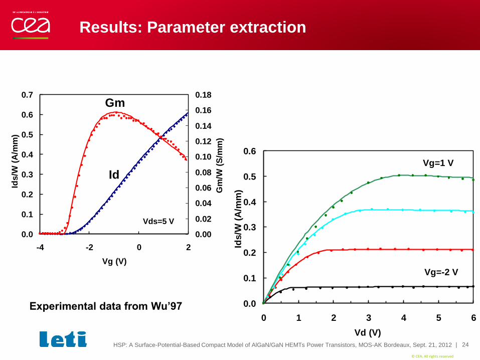
Results: Parameter extraction
Experimental data from Wu’97
0.0
0.1
0.2
0.3
0.4
0.5
0.6
0.7
-4 -2 0 2
Vg (V)
Ids/W
(A
/mm
)
0.00
0.02
0.04
0.06
0.08
0.10
0.12
0.14
0.16
0.18
Gm
/W (
S/m
m)
0.0
0.1
0.2
0.3
0.4
0.5
0.6
0 1 2 3 4 5 6
Vd (V)
Ids/W
(A
/mm
)
Vg=-2 V
Vg=1 V
Id
Gm
Vds=5 V

HSP: A Surface-Potential-Based Compact Model of AlGaN/GaN HEMTs Power Transistors, MOS-AK Bordeaux, Sept. 21, 2012
© CEA. All rights reserved
| 25
Results: DC current and self-heating
Verilog-A code + ADS simulation
L=1 µm and W=75 µm
HSP: A Surface-Potential-Based Compact Model of AlGaN/GaN HEMTs Power Transistors, MOS-AK Bordeaux, Sept. 21, 2012
© CEA. All rights reserved
| 26
Summary and conclusions
HSP: a new approach and attempt for power devices modeling
Physical approach (temperature, Al content, band structure,
SP & PZ polarizations, layer thicknesses, doping, incomplete
donor activation, heat diffusion in substrate, …)
SP approach chosen for continuity of “inversion” charge
Interesting tool for technological development (xAl, Ga- or N-face,
doping, layers thicknesses)
This physical approach allows to estimate the impact of
technological variations on electrical properties (variability)
Further research efforts to improve the core model:
e.g. SHE algorithm convergence for very high temperature
increase (ΔT>300 °C), Schottky gate current, impact of surface
traps, …
Implementation using Verilog-A and ADS simulator from Agilent
HSP: A Surface-Potential-Based Compact Model of AlGaN/GaN HEMTs Power Transistors, MOS-AK Bordeaux, Sept. 21, 2012
© CEA. All rights reserved
| 27
Bibliography
Ambacher O. et al., “Two-dimensional electron gases induced by spontaneous and piezoelectric polarization
charges in N- and Ga-face AlGaN/GaN heterostructures”, Journal of Applied Physics, 85, 3222-3233 (1999).
Angelov I. et al, “On the large-signal modelling of AlGaN/GaN HEMTs and SiC MESFETs”, Gallium Arsenide
and other semiconductor application symposium, 309-312, 2005.
Canfield P.C. et al., “Modeling of frequency and temperature effects in GaAs MESFET’s”, IEEE J. Solid-State
Circuits, 25, 299 (1990).
Cheng X. and Wang Y., “A surface-potential-based compact model for AlGaN/GaN MODFETs”, IEEE Trans.
on Electron Devices, 58, 2, 448-454 (2011).
Curtice W.R. and Ettenberg M., “A Nonlinear GaAs FET model for use in the design of output circuits for
Power amplifiers,” IEEE Trans. on Microwave Theory and Techniques, MTT- 33, 1383-1394 (1985).
Gildenblat G. and Chen T.-L., “Overview of an advanced Surface-Potential-based model (SP)”, Int. Conf.
on Modeling and Simulation of Microsystems, MSM2002.
Götz W. et al., “Activation energies of Si donors in GaN”, Appl. Phys. Lett. 68, 3144 (1996).
Irokawa Y. et al., “Implantation temperature dependence of Si activation in AlGaN”, Appl. Phys. Lett., 88,
182106 (2006).
John D.L. et al., “A surface-potential based model for GaN HEMTs in RF power amplifier applications”,
IEDM 2010, 186-189.
Khandelwal S. and Fjeldly T.A., “A physics based compact model of I-V and C-V characteristics in AlGaN/GaN
HEMT devices”, Solid-State Electronics (76), 60-66 (2012).
Royet A.-S., “Contribution à l’optimisation d’une technologie de composants hyperfréquences réalisés en
Carbure de Silicium (SiC)”, PhD thesis, INP Grenoble (2000).
Schwierz F. et al., “An electron mobility model for wurtzite GaN”, Solid-State Electronics, 49, 889-895 (2005).
Wu Y.-F. et al., “Bias dependent microwave performance of AlGaN/GaN MODFET’s up to 100 V”, IEEE Electron
Devices Letters, 18, 290-292 (1997).
Yu T.-H. and Brennan K.F., “Theoretical Study of a GaN-AlGaN High Electron Mobility Transistor including
a nonlinear polarization model”, IEEE Trans. on Electron Devices, 50, 315-323, (2003).

HSP: A Surface-Potential-Based Compact Model of AlGaN/GaN HEMTs Power Transistors, MOS-AK Bordeaux, Sept. 21, 2012
© CEA. All rights reserved
| 28
Acknowledgements
Many thanks to Luca Lucci
for fruitful discussions on power devices

© CEA. All rights reserved
| PAGE 29 Commissariat à l’énergie atomique et aux énergies alternatives
Centre de Grenoble
Etablissement public à caractère industriel et commercial | RCS Paris B 775 685 019
| PAGE 29
Thank you
for your
attention
www.leti.fr
www.minatec.org