ht32 clock monitor and clock frequency switch
TRANSCRIPT

HT32 Clock Monitor and Clock Frequency Switch
AN0464E 1 / 24 November 11, 2017
HT32 Clock Monitor and Clock Frequency Switch D/N: AN0464E
Introduction This manual will introduce the clock failure detection function and the system frequency
switch about in the HT32 microcontrollers. These microcontrollers are based on the
Cortex-M0 + or Cortex-M3 processor core and support both of these functions.
The clock monitor circuit can be used to detect a clock failure of the external high speed
crystal oscillator, known as HSE. When an HSE oscillator failure occurs, the HSE will be
turned off and the system clock will be switched to the high speed internal RC oscillator
HSI automatically. For more details, refer to the section "HSE clock failure detection".
System clocks can be sourced from HSI, HSE, or the PLL. Some HT32 series
microcontrollers also support an LSI (low speed internal RC oscillator 32kHz) or an LSE
(low speed external crystal oscillator 32kHz) as their system clock. After a reset, the HSI
will be selected as the default system clock. Once a clock source switch occurs, the
software must ensure that the frequency switch process is completed by polling the
system clock switch bit in the Global Clock Control Register, GCCR.
The HSI clock is an internal RC oscillator, which has a fixed frequency of 8MHz, and can
also be used as the PLL input clock. The HSI RC oscillator can be switched on or off
using the HSIEN bit in the Global Clock Control Register, GCCR. When the HSI oscillator
is switched, the HSI clock will not actually be available until the HSIRDY bit has been set
by the hardware.
The high speed external 4 to 16 MHz crystal oscillator, HSE, produces a highly accurate
clock source as the system clock, which can also be used as the PLL input clock. The
HSE RC oscillator can be switched on or off using the HSEEN bit in the Global Clock
Control Register, GCCR. When the HSE oscillator is switched on, the HSE clock will not
be available for use until the HSERDY bit is set by the hardware.
The PLL can provide an 8~144 MHz clock output which is a multiple of a fundamental
reference frequency of 4~16 MHz. When the PLL clock source is switched on, the new
clock source must be ready before being selected. The PLL can be switched on or off by
using the PLLEN bit in the Global Clock Control Register, GCCR. If the PLL clock is
stable, the PLLRDY bit will be set by the hardware.
The low speed internal RC oscillator with a frequency of about 32 kHz produces a low
power clock source for a Real-Time-Clock peripheral, Watchdog Timer or system clock.
The LSI offers a low cost clock source because no external components are required for
its operation. The LSI oscillator is always enabled. The LSI frequency accuracy is shown
in the datasheet. The LSIRDY flag in the Global Clock Status Register, GCSR, will

HT32 Clock Monitor and Clock Frequency Switch
AN0464E 2 / 24 November 11, 2017
indicate if the LSI clock is stable. If the LSI clock is stable, the LSIRDY bit will be set by
the hardware.
The low speed external crystal or ceramic resonator oscillator which has a 32,768 Hz
frequency produces a low power but highly accurate clock source for a Real-Time-Clock
peripheral, Watchdog Timer or system clock. The associated hardware configuration is
shown in the accompanying figure. The crystal or ceramic resonator must be placed
across the two LSE pins, X32KIN/X32KOUT. External components such as resistors and
capacitors are necessary to ensure oscillation takes place. The LSE oscillator can be
switched on or off using the LSEEN bit in the RTC Control Register, RTCCR. The
LSERDY flag in the Global Clock Status Register, GCSR, will indicate if the LSE clock is
stable. If the LSE clock is stable, the LSERDY bit is set by the hardware.
HT32 Clock Control Unit Operation
HSE clock failure detection The HSE Clock Monitor function is enabled by the HSE Clock Monitor Enable bit,
CKMEN, in the Global Clock Control Register, GCCR. The HSE clock monitor function
should be enabled after the HSE oscillator start-up delay has elapsed and disabled when
the HSE oscillator is stopped.
Once an HSE oscillator failure is detected, the HSE oscillator will automatically be
disabled. The HSE clock stuck flag, CKSF, in the Global Clock Interrupt Register, GCIR,
will then be set. An interrupt can be generated if the corresponding clock failure interrupt
enable bit, CKSIE, in GCIR is set. This failure interrupt is connected to the CortexTM-M
Non-Maskable Interrupt NMI. In the NMI interrupt service program, a clock failure
interrupt must be cleared by setting the CKSF bit in the GCIR register.
If the HSE is used as the system clock, when an HSE oscillator failure occurs, the HSE
will be turned off and the system clock will be switched to the HSI automatically by the
hardware.
If the HSE is used as the clock input of the PLL circuit whose output is used as the
system clock, the PLL circuit will also be turned off as well as the HSE when the failure
happens. Here the system clock will be switched to the HSI automatically by the
hardware. The HSE is also used as the clock input of the PLL circuit.
System Frequency Switch The system clock source can be switched by setting a SW bit in the Global Clock Control
Register, GCCR. If the system clock source is switched from one to another, the
destination clock must have first stabilised. The corresponding clock ready status bit in
the Global Clock Status Register, GCSR, will indicate whether the selected clock is ready
to use or not. Once a clock source switch has occurred, then checking if the switching
process has completed is implemented by polling a SW bit in the GCCR register. The SW
bit needs to be read to set the new clock source.

HT32 Clock Monitor and Clock Frequency Switch
AN0464E 3 / 24 November 11, 2017
The system frequency also can be switched without turning off the PLL in the PLL
configuration option. The steps to switch system frequency are as follows:
1. Select HSE or HSI as the system clock (SW[1:0]=0×2 or 0×3). The HSE or the HSI should be first ready.
2. Poll the SW bit until the pre-written value is valid.
3. Setup the AHB prescaler by setting the AHBPRE bit (AHBPRE[1:0]=0×0).
4. Reconfigure the PLL output frequency by setting the PLLCFGR register. The PLL is enabled.
5. Poll the PLLRDY bit until the flag bit in the GCSR register is set high.
6. Set AHBPRE bit.
7. Set the WAIT bit and control the flickering wait status.
8. Select the PLL as the system clock (SW[1:0]=0×0 or 0×1)
9. Poll the SW bit until the pre-written value is valid.
Select HSI or HSE as system clock
Poll System Clock Switch
Set AHB Prescaler as 0x0
Reconfigure PLL frequency
Start
Is PLL ready ?
Set AHB Prescaler
Set Flash Wait State
Select PLL as system clock
Poll System Clock Switch
Finish
Yes
No
Figure 1 System Frequency Switch Flow Chart

HT32 Clock Monitor and Clock Frequency Switch
AN0464E 4 / 24 November 11, 2017
Register Descriptions The following table shows the CKCU register and reset values.
Register Offset Description Reset Value FMC Base Address = 0x4008_8000
GCFGR 0x000 Global Clock Configuration Register 0x0000_0102 GCCR 0x004 Global Clock Control Register 0x0000_0803 GCSR 0x008 Global Clock Status Register 0x0000_0028 GCIR 0x00C Global Clock Interrupt Register 0x0000_0000
PLLCFGR 0x018 PLL Configuration Register 0x0000_0000 PLLCR 0x01C PLL Control Register 0x0000_0000
AHBCFGR 0x020 AHB Configuration Register 0x0000_0000 AHBCCR 0x024 AHB Clock Control Register 0x0000_0005
APBCFGR 0x028 APB Configuration Register 0x0000_0000 APBCCR0 0x02C APB Clock Control Register 0 0x0000_0000 APBCCR1 0x030 APB Clock Control Register 1 0x0000_0000
CKST 0x034 Clock Source Status Register 0x0100_0000 APBPCSR0 0x038 APB Peripheral Clock Selection Register 0 0x0000_0000 APBPCSR1 0x03C APB Peripheral Clock Selection Register 1 0x0000_0000
HSICR 0x040 HSI Control Register 0xXXXX_0000 (where X is undefined) HSIATCR 0x044 HSI Auto Trimming Counter Register 0x0000_0000
LPCR 0x300 Low Power Control Register 0x0000_0000 MCUDBGCR 0x304 MCU Debug Control Register 0x0000_0000
Table 1 CKCU Registers

HT32 Clock Monitor and Clock Frequency Switch
AN0464E 5 / 24 November 11, 2017
Global Clock Configuration Register – GCFGR This register specifies the clock source for the PLL/USART/WDT/CKOUT.
Offset: 0x000
Reset value: 0x0000_0102
31 30 29 28 27 26 25 24
LPMOD Reserved
Type/Reset RO 0 RO 0 RO 0
23 22 21 20 19 18 17 16
Reserved URPRE Reserved
Type/Reset RW 0 RW 0
15 14 13 12 11 10 9 8
Reserved PLLSRC
Type/Reset RW 1
7 6 5 4 3 2 1 0
Reserved WDTSRC CKOUTSRC
Type/Reset RW 0 RW 0 RW 1 RW 0
Bits Field Description
[31:29] LPMOD Lower Power Mode Status
Set and reset by hardware.
b000: When in running mode
b001: To enter the Sleep Mode
b010: To enter the Deep Sleep Mode1
b011: To enter the Deep Sleep Mode2
b100: To enter the Power Down mode
Others: Reserved
[21:20] URPRE USART Clock Prescaler Selection
Set and reset by software to control the USART clock prescaler setting.
b00: CK_USART = CK_UR
b01: CK_USART = CK_UR / 2
Others: Reserved
[8] PLLSRC PLL Clock Source Selection
Set and reset by software to control the PLL clock source.
0: External 4 ~ 16 MHz crystal oscillator–HSE
1: External 4 ~ 16 MHz crystal oscillator–HSI
[3] WDTSRC Watchdog Timer Clock Source Selection
Set and reset by software to control the Watchdog Timer clock source.
0: Internal 32kHz RC oscillator–LSI
1: External 32768Hz crystal oscillator–LSE
[2:0] CKOUTSRC CKOUT Clock Source Selection
Set and reset by software.
000: CK_PLL / 16
001: CK_AHB / 16
010: CK_SYS / 16
011: CK_HSE / 16
100: CK_HSI / 16
101: CK_LSE
110: CK_LSI
111: Reserved

HT32 Clock Monitor and Clock Frequency Switch
AN0464E 6 / 24 November 11, 2017
Global Clock Control Register – GCCR This register specifies the clock enable bits.
Offset: 0x004
Reset value: 0x0000_0803
31 30 29 28 27 26 25 24
Reserved
Type/Reset
23 22 21 20 19 18 17 16
Reserved PSRCEN CKMEN
Type/Reset RW 0 RW 0
15 14 13 12 11 10 9 8
Reserved HSIEN HSEEN PLLEN Reserved
Type/Reset RW 1 RW 0 RW 0
7 6 5 4 3 2 1 0
Reserved SW
Type/Reset RW 1 RW 1
Bits Field Descriptions
[17] PSRCEN Power Saving Wakeup RC Clock Enable
0: No action
1: Use the internal 8 MHz RC clock (HSI) as the system clock after a Deep Sleep 1/2
wakeup.
The software can set the PSRCEN bit high before entering the power saving mode. In
order to reduce the waiting time after a wakeup. When the PSRCEN bit is set to 1, the
HSI will be used as the CK_SYS clock source after waking up from the Deep Sleep1 or
Deep Sleep2 mode. This means that the instructions can be executed before the original
CK_SYS source is stable since the HSI clock is provided to the CortexTM-M3. After the
original clock source is ready, the CK_SYS clock will automatically be switched back to
the original before entering the Deep Sleep1 or Deep Sleep2 mode
[16] CKMEN HSE Clock Monitor Enable
0: Disable External 4 ~ 16 MHz crystal oscillator HSE clock monitor
1: Enable External 4 ~ 16 MHz crystal oscillator HSE clock monitor
When the hardware detects that the HSE clock is stuck at a low or high state, the internal
hardware will switch the system clock to the internal high speed HSI RC clock. The way to
recover the system clock is by an external reset, a power on reset or clearing the CKSF
by software.
Note: When the HSE clock monitor is enabled, the hardware will automatically turn on the
internal RC oscillator HSI regardless of the state of the HSIEN control bit.
[11] HSIEN Internal High Speed Oscillator Enable
Set and reset by software. This bit cannot be reset if the HSI clock is used as the system
clock.
0: Internal 8 MHz RC oscillator is disabled
1: Internal 8 MHz RC oscillator is enabled
[10] HSEEN External High Speed Oscillator Enable
Set and reset by software. This bit cannot be reset if the HSE clock is used as the system
clock or the PLL input clock.
0: External 4 ~ 16 MHz crystal oscillator is disabled
1: External 4 ~ 16 MHz crystal oscillator is enabled

HT32 Clock Monitor and Clock Frequency Switch
AN0464E 7 / 24 November 11, 2017
Bits Field Descriptions
[9] PLLEN PLL Enable
Set and reset by software. This bit cannot be reset if the PLL clock is used as the system
clock.
0: PLL is disabled
1: PLL is enabled
[1:0] SW System Clock Switch
This bit field is set and reset by software to select the CK_SYS source. The HSI oscillator
(SW[1:0]=0x03)will be forced for use as the system clock directly or indirectly when an
HSE clock failure is detected as the HSE clock monitor function is enabled. This bit field
can be read back by software to indicate which clock is currently used as the system
clock. The system clock will not be immediately switched and a certain delay is
necessary. This delay is determined by software.
0X: CK_PLL clock out as system clock
10: CK_HSE as system clock
11: CK_HSI as system clock
Global Clock Status Register – GCSR This register indicates the clock ready status.
Offset: 0x008
Reset value: 0x0000_0028
31 30 29 28 27 26 25 24
Reserved
Type/Reset
23 22 21 20 19 18 17 16
Reserved
Type/Reset
15 14 13 12 11 10 9 8
Reserved
Type/Reset
7 6 5 4 3 2 1 0
Reserved LSIRDY LSERDY HSIRDY HSERDY PLLRDY Reserved
Type/Reset RO 1 RO 0 RO 1 RO 0 RO 0
Bits Field Descriptions
[5] LSIRDY Internal Low Speed Oscillator LSI Ready Flag
Set by hardware to indicate whether the LSI is stable and can be used.
0: Internal 32 kHz RC oscillator is not ready
1: Internal 32 kHz RC oscillator is ready
[4] LSERDY External Low Speed Oscillator LSE Ready Flag
Set by hardware to indicate whether the LSE is stable and can be used.
0: LSE oscillator is not ready
1: LSE oscillator is ready
[3] HSIRDY Internal High Speed Oscillator HSI Ready Flag
Set by hardware to indicate whether the HSI is stable and can be used.
0: HSI oscillator is not ready
1: HSI oscillator is ready
[2] HSERDY External High Speed Oscillator Ready Flag
Set by hardware to indicate whether the HSE is stable and can be used.
0: HSE oscillator is not ready
1: HSE oscillator is ready

HT32 Clock Monitor and Clock Frequency Switch
AN0464E 8 / 24 November 11, 2017
Bits Field Descriptions
[1] PLLRDY PLL Clock Ready Flag
Set by hardware to indicate whether the PLL output is stable and can be used.
0: PLL is not ready
1: PLL is ready
Global Clock Interrupt Register – GCIR This register specifies the interrupt enable and flag bits.
Offset: 0x00C
Reset value: 0x0000_0000
31 30 29 28 27 26 25 24
Reserved
Type/Reset
23 22 21 20 19 18 17 16
Reserved LSIRDYIE LSERDYIE HSIRDYIE HSERDYIE PLLRDYIE Reserved CKSIE
Type/Reset RW 0 RW 0 RW 0 RW 0 RW 0 RW 0
15 14 13 12 11 10 9 8
Reserved
Type/Reset
7 6 5 4 3 2 1 0
Reserved LSIRDYF LSERDYF HSIRDYF HSERDYF PLLRDYF Reserved CKSF
Type/Reset WC 0 WC 0 WC 0 WC 0 WC 0 WC 0
Bits Field Descriptions
[22] LSIRDYIE LSI Ready Interrupt Enable
Set and reset by software to enable/disable interrupt caused by LSI stabilization.
0: Disable LSI stabilization interrupt
1: Enable LSI stabilization interrupt
[21] LSERDYIE LSE Ready Interrupt Enable
Set and reset by software to enable/disable interrupt caused by LSE stabilization.
0: Disable LSE stabilization interrupt
1: Enable LSE stabilization interrupt
[20] HSIRDYIE HSI Ready Interrupt Enable
Set and reset by software to enable/disable interrupt caused by HSI stabilization.
0: Disable HSI stabilization interrupt
1: Enable HSI stabilization interrupt
[19] HSERDYIE HSE Ready Interrupt Enable
Set and reset by software to enable/disable interrupt caused by HSE stabilization.
0: Disable HSE stabilization interrupt
1: Enable HSE stabilization interrupt
[18] PLLRDYIE PLL Ready Interrupt Enable
Set and reset by software to enable/disable interrupt caused by PLL stabilization.
0: Disable PLL stabilization interrupt
1: Enable PLL stabilization interrupt
[16] CKSIE Clock Stuck Interrupt Enable
Set and reset by software to enable or disable the clock failure interrupt caused by
clock monitor.
0: Disable clock failure interrupt
1: Enable clock failure interrupt

HT32 Clock Monitor and Clock Frequency Switch
AN0464E 9 / 24 November 11, 2017
Bits Field Descriptions
[6] LSIRDYF LSI Ready Interrupt Flag
Reset by software (Write 1 clear). Set by hardware when the internal 32 kHz RC
oscillator clock stabilization and LSIRDYDIE are set.
0: No LSI stabilization clock ready interrupt event has occurred
1: Clock ready interrupt caused by LSI stabilization
[5] LSERDYF LSE Ready Interrupt Flag
Reset by software (Write 1 clear). Set by hardware when the external 32,768 Hz
crystal oscillator clock stabilization and LSERDYDIE are set.
0: No clock ready interrupt caused by LSE stabilization
1: Clock ready interrupt caused by LSE stabilization
[4] HSIRDYF HSI Ready Interrupt Flag
Reset by software (Write 1 clear). Set by hardware when the internal 8 MHz RC
oscillator clock stabilization and HSIRDYDIE is set.
0: No clock ready interrupt caused by HSI stabilization
1: Clock ready interrupt caused by HSI stabilization
[3] HSERDYF HSE Ready Interrupt Flag
Reset by software (Write 1 clear). Set by hardware when the external 4 ~ 16 MHz
crystal oscillator clock stabilization and HSERDYDIE are set.
0: No clock ready interrupt caused by HSE stabilization
1: Clock ready interrupt caused by HSE stabilization
[2] PLLRDYF PLL Ready Interrupt Flag
Reset by software (Write 1 clear). Set by hardware when the PLL stabilization and
PLLRDYDIE are set.
0: Clock not ready interrupt caused by PLL stabilization
1: Clock ready interrupt caused by PLL stabilization
[0] CKSF HSE Clock Stuck Interrupt Flag
Reset by software (Write 1 clear). Set by hardware when the HSE clock is stuck and
the CKSIE bit is set.
0: Clock works normally
1: HSE clock is stuck
HT32 Clock Monitor and Clock Frequency Switch
AN0464E 10 / 24 November 11, 2017
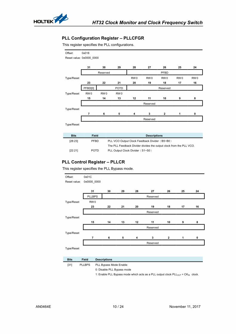
PLL Configuration Register – PLLCFGR This register specifies the PLL configurations.
Offset: 0x018
Reset value: 0x0000_0000
31 30 29 28 27 26 25 24
Reserved PFBD
Type/Reset RW 0 RW 0 RW 0 RW 0 RW 0
23 22 21 20 19 18 17 16
PFBD[0] POTD Reserved
Type/Reset RW 0 RW 0 RW 0
15 14 13 12 11 10 9 8
Reserved
Type/Reset
7 6 5 4 3 2 1 0
Reserved
Type/Reset
Bits Field Descriptions
[28:23] PFBD PLL VCO Output Clock Feedback Divider(B5~B0)
The PLL Feedback Divider divides the output clock from the PLL VCO.
[22:21] POTD PLL Output Clock Divider(S1~S0)
PLL Control Register – PLLCR This register specifies the PLL Bypass mode.
Offset: 0x01C
Reset value: 0x0000_0000
31 30 29 28 27 26 25 24
PLLBPS Reserved
Type/Reset RW 0
23 22 21 20 19 18 17 16
Reserved
Type/Reset
15 14 13 12 11 10 9 8
Reserved
Type/Reset
7 6 5 4 3 2 1 0
Reserved
Type/Reset
Bits Field Descriptions
[31] PLLBPS PLL Bypass Mode Enable
0: Disable PLL Bypass mode
1: Enable PLL Bypass mode which acts as a PLL output clock PLLOUT = CKIN clock.

HT32 Clock Monitor and Clock Frequency Switch
AN0464E 11 / 24 November 11, 2017
AHB Configuration Register – AHBCFGR This register specifies the system clock frequency.
Offset: 0x020
Reset value: 0x0000_0000
31 30 29 28 27 26 25 24
Reserved
Type/Reset
23 22 21 20 19 18 17 16
Reserved
Type/Reset
15 14 13 12 11 10 9 8
Reserved
Type/Reset
7 6 5 4 3 2 1 0
Reserved AHBPRE
Type/Reset RW 0 RW 0
Bits Field Descriptions
[1:0] AHBPRE AHB Prescaler
Set and reset by software to control the division ratio of the AHB clock.
00: CK_AHB = CK_SYS
01: CK_AHB = CK_SYS / 2
10: CK_AHB = CK_SYS / 4
11: CK_AHB = CK_SYS / 8

HT32 Clock Monitor and Clock Frequency Switch
AN0464E 12 / 24 November 11, 2017
AHB Clock Control Register–AHBCCR This register specifies the AHB clock enable bits.
Offset: 0x024
Reset value: 0x0000_0005
31 30 29 28 27 26 25 24
Reserved
Type/Reset
23 22 21 20 19 18 17 16
Reserved
Type/Reset
15 14 13 12 11 10 9 8
Reserved
Type/Reset
7 6 5 4 3 2 1 0
Reserved SRAMEN Reserved FMCEN
Type/Reset RW 1 RW 1
Bits Field Descriptions
[2] SRAMEN SRAM Clock Enable
Set and reset by software. The user can clear the SRAMEN bit to 0 to reduce power
consumption if the SRAM is unused in the Sleep mode.
0: SRAM clock is automatically disabled by hardware in the Sleep mode
1: SRAM clock is always enabled in the Sleep mode
[0] FMCEN Flash Memory Controller Clock Enable
Set and reset by software. The user can clear the FMCEN bit to 0 to reduce power
consumption if the Flash Memory is unused in the Sleep mode.
0: FMC clock is automatically disabled by hardware in the Sleep mode
1: FMC clock is always enabled in the Sleep mode

HT32 Clock Monitor and Clock Frequency Switch
AN0464E 13 / 24 November 11, 2017
APB Configuration Register – APBCFGR This register specifies the ADC conversion clock frequency.
Offset: 0x028
Reset value: 0x0000_0000
31 30 29 28 27 26 25 24
Reserved
Type/Reset
23 22 21 20 19 18 17 16
Reserved ADCDIV
Type/Reset RW 0 RW 0 RW 0
15 14 13 12 11 10 9 8
Reserved
Type/Reset
7 6 5 4 3 2 1 0
Reserved
Type/Reset
Bits Field Descriptions
[18:16] ADCDIV ADC Clock Frequency Division Selection
Set and reset by software to control the ADC conversion clock division ratio.
000: CK_ADC = CK_AHB
001: CK_ADC = (CK_AHB / 2)
010: CK_ADC = (CK_AHB / 4)
011: CK_ADC = (CK_AHB / 8)
100: CK_ADC = (CK_AHB / 16)
101: CK_ADC = (CK_AHB / 32)
110: CK_ADC = (CK_AHB / 64)
111: CK_ADC = (CK_AHB / 6)

HT32 Clock Monitor and Clock Frequency Switch
AN0464E 14 / 24 November 11, 2017
APB Clock Control Register 0 – APBCCR0 This register specifies the APB peripherals clock enable bits.
Offset: 0x02C
Reset value: 0x0000_0000
31 30 29 28 27 26 25 24
Reserved
Type/Reset
23 22 21 20 19 18 17 16
Reserved PBEN PAEN
Type/Reset RW 0 RW 0
15 14 13 12 11 10 9 8
EXTIEN AFIOEN Reserved UREN
Type/Reset RW 0 RW 0 RW 0
7 6 5 4 3 2 1 0
Reserved SPIEN Reserved I2CEN
Type/Reset RW 0 RW 0
Bits Field Descriptions
[17] PBEN GPIO Port B Clock Enable
Set and reset by software.
0: Port B Clock is disabled
1: Port B Clock is enabled
[16] PAEN GPIO Port A Clock Enable
Set and reset by software.
0: Port A Clock is disabled
1: Port A Clock is enabled
[15] EXTIEN External Interrupt Clock Enable
Set and reset by software.
0: EXTI Clock is disabled
1: EXTI Clock is enabled
[14] AFIOEN Alternate Function I/O Clock Enable
Set and reset by software.
0: AFIO Clock is disabled
1: AFIO Clock is enabled
[8] UREN USART Clock Enable
Set and reset by software.
0: USART Clock is disabled
1: USART Clock is enabled
[4] SPIEN SPI Clock Enable
Set and reset by software.
0: SPI Clock is disabled
1: SPI Clock is enabled
[0] I2CEN I2C Clock Enable
Set and reset by software.
0: I2C Clock is disabled
1: I2C Clock is enabled

HT32 Clock Monitor and Clock Frequency Switch
AN0464E 15 / 24 November 11, 2017
APB Clock Control Register 1 – APBCCR1 This register specifies the APB peripherals clock enable bits.
Offset: 0x030
Reset value: 0x0000_0000
31 30 29 28 27 26 25 24
Reserved ADCEN
Type/Reset RW 0
23 22 21 20 19 18 17 16
OPA1EN OPA0EN Reserved
Type/Reset RW 0 RW 0
15 14 13 12 11 10 9 8
Reserved GPTM1EN GPTM0EN
Type/Reset RW 0 RW 0
7 6 5 4 3 2 1 0
Reserved RTCEN Reserved WDTEN Reserved
Type/Reset RW 0 RW 0
Bits Field Descriptions
[24] ADCEN ADC Clock Enable
Set and reset by software.
0: ADC clock is disabled
1: ADC clock is enabled
[23] OPA1EN OPA/CMP 1 Clock Enable
Set and reset by software.
0: OPA/CMP 1 clock is disabled
1: OPA/CMP 1 clock is enabled
[22] OPA0EN OPA/CMP 0 Clock Enable
Set and reset by software.
0: OPA/CMP 0 clock is disabled
1: OPA/CMP 0 clock is enabled
[9] GPTM1EN GPTM1 Clock Enable
Set and reset by software.
0: GPTM1 clock is disabled
1: GPTM1 clock is enabled
[8] GPTM0EN GPTM0 Clock Enable
Set and reset by software.
0: GPTM0 clock is disabled
1: GPTM0 clock is enabled
[6] RTCEN RTC Clock Enable
Set and reset by software.
0: RTC clock is disabled
1: RTC clock is enabled
[4] WDTEN Watchdog Timer Clock Enable
Set and reset by software.
0: Watchdog Timer clock is disabled
1: Watchdog Timer clock is enabled

HT32 Clock Monitor and Clock Frequency Switch
AN0464E 16 / 24 November 11, 2017
Clock Source Status Register – CKST This register specifies the clock source status.
Offset: 0x034
Reset value: 0x0100_0000
31 30 29 28 27 26 25 24
Reserved HSIST
Type/Reset RO 0 RO 0 RO 1
23 22 21 20 19 18 17 16
Reserved HSEST
Type/Reset RO 0 RO 0
15 14 13 12 11 10 9 8
Reserved PLLST
Type/Reset RO 0
7 6 5 4 3 2 1 0
Reserved
Type/Reset
Bits Field Descriptions
[26:24] HSIST Internal High Speed Clock Occupation Status (CK_HSI)
xx1: HSI is used by the System Clock (CK_SYS)(SW=0x03)
x1x: HSI is used by the PLL
1xx: HSI is used by the Clock Monitor
[17:16] HSEST External High Speed Clock Occupation Status (CK_HSE)
x1: HSE is used by the System Clock (CK_SYS)(SW=0x02)
1x: HSE is used by the PLL
[8] PLLST PLL Clock Occupation Status
0: PLL is not used by the System Clock (CK_SYS)
1: PLL is used by the System Clock (CK_SYS)

HT32 Clock Monitor and Clock Frequency Switch
AN0464E 17 / 24 November 11, 2017
APB Peripheral Clock Selection Register 0 – APBPCSR0 This register specifies the APB peripheral clock prescaler selection.
Offset: 0x038
Reset value: 0x0000_0000
31 30 29 28 27 26 25 24
UR1PCLK UR0PCLK USR1PCLK USR0PCLK
Type/Reset RW 0 RW 0 RW 0 RW 0 RW 0 RW 0 RW 0 RW 0
23 22 21 20 19 18 17 16
GPTM1PCLK GPTM0PCLK MCTM1PCLK MCTM0PCLK
Type/Reset RW 0 RW 0 RW 0 RW 0 RW 0 RW 0 RW 0 RW 0
15 14 13 12 11 10 9 8
BFTM1PCLK BFTM0PCLK Reserved
Type/Reset RW 0 RW 0 RW 0 RW 0
7 6 5 4 3 2 1 0
SPI1PCLK SPI0PCLK I2C1PCLK I2C0PCLK
Type/Reset RW 0 RW 0 RW 0 RW 0 RW 0 RW 0 RW 0 RW 0
Bits Field Descriptions
[31:30] UR1PCLK UART1 Peripheral Clock Selection
00: PCLK = CK_AHB
01: PCLK = CK_AHB / 2
10: PCLK = CK_AHB / 4
11: PCLK = CK_AHB / 8
PCLK = Peripheral Clock; CK_AHB = AHB and CPU clock
[29:28] UR0PCLK UART0 Peripheral Clock Selection
00: PCLK = CK_AHB
01: PCLK = CK_AHB / 2
10: PCLK = CK_AHB / 4
11: PCLK = CK_AHB / 8
PCLK = Peripheral Clock; CK_AHB = AHB and CPU clock
[27:26] USR1PCLK USART1 Peripheral Clock Selection
00: PCLK = CK_AHB
01: PCLK = CK_AHB / 2
10: PCLK = CK_AHB / 4
11: PCLK = CK_AHB / 8
PCLK = Peripheral Clock; CK_AHB = AHB and CPU clock
[25:24] USR0PCLK USART0 Peripheral Clock Selection
00: PCLK = CK_AHB
01: PCLK = CK_AHB / 2
10: PCLK = CK_AHB / 4
11: PCLK = CK_AHB / 8
PCLK = Peripheral Clock; CK_AHB = AHB and CPU clock
[23:22] GPTM1PCLK GPTM1 Peripheral Clock Selection
00: PCLK = CK_AHB
01: PCLK = CK_AHB / 2
10: PCLK = CK_AHB / 4
11: PCLK = CK_AHB / 8
PCLK = Peripheral Clock; CK_AHB = AHB and CPU clock

HT32 Clock Monitor and Clock Frequency Switch
AN0464E 18 / 24 November 11, 2017
Bits Field Descriptions
[21:20] GPTM0PCLK GPTM0 Peripheral Clock Selection
00: PCLK = CK_AHB
01: PCLK = CK_AHB / 2
10: PCLK = CK_AHB / 4
11: PCLK = CK_AHB / 8
PCLK = Peripheral Clock; CK_AHB = AHB and CPU clock
[19:18] MCTM1PCLK MCTM1 Peripheral Clock Selection
00: PCLK = CK_AHB
01: PCLK = CK_AHB / 2
10: PCLK = CK_AHB / 4
11: PCLK = CK_AHB / 8
PCLK = Peripheral Clock; CK_AHB = AHB 和 CPU clock
[17:16] MCTM0PCLK MCTM0 Peripheral Clock Selection
00: PCLK = CK_AHB
01: PCLK = CK_AHB / 2
10: PCLK = CK_AHB / 4
11: PCLK = CK_AHB / 8
PCLK = Peripheral Clock; CK_AHB = AHB and CPU clock
[15:14] BFTM1PCLK BFTM1 Peripheral Clock Selection
00: PCLK = CK_AHB
01: PCLK = CK_AHB/2
10: PCLK = CK_AHB/4
11: PCLK = CK_AHB/8
PCLK = Peripheral Clock; CK_AHB = AHB and CPU clock
[13:12] BFTM0PCLK BFTM0 Peripheral Clock Selection
00: PCLK = CK_AHB
01: PCLK = CK_AHB / 2
10: PCLK = CK_AHB / 4
11: PCLK = CK_AHB / 8
PCLK = Peripheral Clock; CK_AHB = AHB and CPU clock
[7:6] SPI1PCLK SPI1 Peripheral Clock Selection
00: PCLK = CK_AHB
01: PCLK = CK_AHB / 2
10: PCLK = CK_AHB / 4
11: PCLK = CK_AHB / 8
PCLK = Peripheral Clock; CK_AHB = AHB and CPU clock
[5:4] SPI0PCLK SPI0 Peripheral Clock Selection
00: PCLK = CK_AHB
01: PCLK = CK_AHB / 2
10: PCLK = CK_AHB / 4
11: PCLK = CK_AHB / 8
PCLK = Peripheral Clock; CK_AHB = AHB and CPU clock
[3:2] I2C1PCLK I2C1 Peripheral Clock Selection
00: PCLK = CK_AHB
01: PCLK = CK_AHB / 2
10: PCLK = CK_AHB / 4
11: PCLK = CK_AHB / 8
PCLK = Peripheral Clock; CK_AHB = AHB and CPU clock
[1:0] I2C0PCLK I2C0 Peripheral Clock Selection
00: PCLK = CK_AHB
01: PCLK = CK_AHB / 2
10: PCLK = CK_AHB / 4
11: PCLK = CK_AHB / 8
PCLK = Peripheral Clock; CK_AHB = AHB and CPU clock

HT32 Clock Monitor and Clock Frequency Switch
AN0464E 19 / 24 November 11, 2017
APB Peripheral Clock Selection Register 1 – APBPCSR1
This register specifies the APB peripheral clock prescaler selection.
Offset: 0x03C
Reset value: 0x0000_0000
31 30 29 28 27 26 25 24
Reserved
Type/Reset
23 22 21 20 19 18 17 16
Reserved I2SPCLK SCI1PCLK SCI0PCLK
Type/Reset RW 0 RW 0 RW 0 RW 0 RW 0 RW 0
15 14 13 12 11 10 9 8
BKPRPCLK WDTRPCLK Reserved CMPPCLK
Type/Reset RW 0 RW 0 RW 0 RW 0 RW 0 RW 0
7 6 5 4 3 2 1 0
Reserved ADCCPCLK EXTIPCLK AFIOPCLK
Type/Reset RW 0 RW 0 RW 0 RW 0 RW 0 RW 0
Bits Field Descriptions
[21:20] I2SPCLK I2S Peripheral Clock Selection
00: PCLK = CK_AH
01: PCLK = CK_AHB / 2
10: PCLK = CK_AHB / 4
11: PCLK = CK_AHB / 8
PCLK = Peripheral Clock; CK_AHB = AHB and CPU clock
[19:18] SCI1PCLK SCI1 Peripheral Clock Selection
00: PCLK = CK_AHB
01: PCLK = CK_AHB / 2
10: PCLK = CK_AHB / 4
11: PCLK = CK_AHB / 8
PCLK = Peripheral Clock; CK_AHB = AHB and CPU clock
[17:16] SCI0PCLK SCI1 Peripheral Clock Selection
00: PCLK = CK_AHB
01: PCLK = CK_AHB / 2
10: PCLK = CK_AHB / 4
11: PCLK = CK_AHB / 8
PCLK = Peripheral Clock; CK_AHB = AHB and CPU clock
[15:14] BKPRCLK Backup Domain Register Access Clock Selection
00: PCLK = CK_AHB / 4
01: PCLK = CK_AHB / 8
10: PCLK = CK_AHB / 16
11: PCLK = CK_AHB / 32
PCLK = Peripheral Clock; CK_AHB = AHB and CPU clock
[13:12] WDTRPCLK WDT Register Access Clock Selection
00: PCLK = CK_AHB
01: PCLK = CK_AHB / 2
10: PCLK = CK_AHB / 4
11: PCLK = CK_AHB / 8
PCLK = Peripheral Clock; CK_AHB = AHB and CPU clock

HT32 Clock Monitor and Clock Frequency Switch
AN0464E 20 / 24 November 11, 2017
Bits Field Descriptions
[9:8] CMPPCLK CMP Peripheral Clock Selection
00: PCLK = CK_AHB
01: PCLK = CK_AHB / 2
10: PCLK = CK_AHB / 4
11: PCLK = CK_AHB / 8
PCLK = Peripheral Clock; CK_AHB = AHB and CPU clock
[5:4] ADCCPCLK ADC Peripheral Clock Selection
00: PCLK = CK_AHB
01: PCLK = CK_AHB / 2
10: PCLK = CK_AHB / 4
11: PCLK = CK_AHB / 8
PCLK = Peripheral Clock; CK_AHB = AHB and CPU clock
[3:2] EXTIPCLK EXTI Peripheral Clock Selection
00: PCLK = CK_AHB
01: PCLK = CK_AHB / 2
10: PCLK = CK_AHB / 4
11: PCLK = CK_AHB / 8
PCLK = Peripheral Clock; CK_AHB = AHB and CPU clock
[1:0] AFIOPCLK AFIO Peripheral Clock Selection
00: PCLK = CK_AHB
01: PCLK = CK_AHB / 2
10: PCLK = CK_AHB / 4
11: PCLK = CK_AHB / 8
PCLK = Peripheral Clock; CK_AHB = AHB and CPU clock
HSI Control Register – HSICR This register is used to control the HSI RC oscillator frequency trimming.
Offset: 0x040
Reset value: 0xXXXX_0000 where X is undefined
31 30 29 28 27 26 25 24
Reserved HSICOARSE
Type/Reset RO X RO X RO X RO X RO X
23 22 21 20 19 18 17 16
HSIFINE
Type/Reset RW X RW X RW X RW X RW X RW X RW X RW X
15 14 13 12 11 10 9 8
Reserved
Type/Reset
7 6 5 4 3 2 1 0
FLOCK REFCLKSEL TMSEL Reserved ATCEN TRIMEN
Type/Reset RO 0 RW 0 RW 0 RW 0 RW 0 RW 0
Bits Field Descriptions
[28:24] HSICOARSE HIS Clock Coarse Trimming Value These bits are initialized automatically at startup. They are adjusted during factory trimming and cannot be trimmed by the application program.

HT32 Clock Monitor and Clock Frequency Switch
AN0464E 21 / 24 November 11, 2017
Bits Field Descriptions
[23:16] HSIFINE HSI Clock Fine Trimming Value These bits are initialized automatically at startup. They are also adjusted during factory trimming. However these bits provide an additional user-programmable trimming value that is added to the HSICOARSE[4:0] bits to obtain higher accuracy or compensate the variations in voltage and temperature that influence the HSI frequency. It can be programmed by software or by the Auto-Trimming Controller (ATC) with an external reference clock.
[7] FLOCK Frequency Lock 0: HSI frequency is not trimmed into target range. 1: HSI frequency is trimmed into target range.
[6:5] REFCLKSEL Reference Clock Selection 0: 32.768 kHz external low speed clock (LSE) 1: 1kHz USB frame pulse This bit is used to select the reference clock for the HSI Auto Trimming Controller.
[4] TMSEL Trimming Mode Selection 0: Automatic by Auto Trimming Controller 1: Manual by user program This bit is used to select the HSI RC oscillator trimming function by the ATC hardware or user program via the HSIFINE[7:0] bits in the HSI Control Register.
[1] ATCEN Auto Trimming Controller Enable 0: Disable Auto Trimming Controller 1: Enable Auto Trimming Controller
[0] TRIMEN Trimming Enable 0:HSI Trimming is disabled 1:HSI Trimming is enabled The bit enables the HSI RC oscillator trimming function using the ATC hardware or user program.
HSI Auto Trimming Counter Register – HSIATCR This register contains the counter value of the HSI auto trimming controller.
Offset: 0x044
Reset value: 0x0000_0000
31 30 29 28 27 26 25 24
Reserved
Type/Reset
23 22 21 20 19 18 17 16
Reserved
Type/Reset
15 14 13 12 11 10 9 8
Reserved ATCNT
Type/Reset RO 0 RO 0 RO 0 RO 0 RO 0 RO 0
7 6 5 4 3 2 1 0
ATCNT
Type/Reset RO 0 RO 0 RO 0 RO 0 RO 0 RO 0 RO 0 RO 0
Bits Field Descriptions
[13:0] ATCNT Auto Trimming Counter These bits are the counter value of the HSI auto trimming controller.

HT32 Clock Monitor and Clock Frequency Switch
AN0464E 22 / 24 November 11, 2017
Low Power Control Register – LPCR This register specifies the low power control.
Offset: 0x300
Reset value: 0x0000_0000
31 30 29 28 27 26 25 24
Reserved
Type/Reset
23 22 21 20 19 18 17 16
Reserved
Type/Reset
15 14 13 12 11 10 9 8
Reserved
Type/Reset
7 6 5 4 3 2 1 0
Reserved BKISO
Type/Reset R/W 0
Bits Field Descriptions
[0] BKISO Backup Domain Isolation Control
Set and reset by software. Refer to the Reference Power Control Unit
chapter for more information.
0: Backup domain is isolated from other power domains.
1: Backup domain is accessible by other power domains.
MCU Debug Control Register – MCUDBGCR This register specifies the MCU debug control.
Offset: 0x304
Reset value: 0x0000_0000
31 30 29 28 27 26 25 24
Reserved
Type/Reset
23 22 21 20 19 18 17 16
Reserved
Type/Reset
15 14 13 12 11 10 9 8
Reserved DBDSLP2 Reserved DBSPI Reserved DBUSART
Type/Reset R/W 0 R/W 0 R/W 0
7 6 5 4 3 2 1 0
DBGPTM1 DBGPTM0 Reserved DBWDT DBPD DBDSLP1 DBSLP
Type/Reset R/W 0 R/W 0 R/W 0 R/W 0 R/W 0 R/W 0
Bits Field Descriptions
[14] DBDSLP2 Debug Deep-Sleep 2
Set and reset by software.
0 :LDO = Off, DMOS = On, FCLK = Off and HCLK = Off in Deep-Sleep 2
1:LDO = On, FCLK = On and HCLK = On in Deep-Sleep 2
HT32 Clock Monitor and Clock Frequency Switch
AN0464E 23 / 24 November 11, 2017
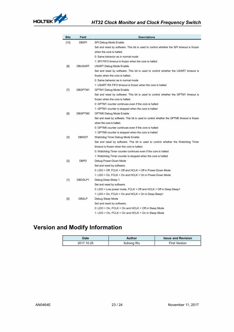
Bits Field Descriptions
[10] DBSPI SPI Debug Mode Enable
Set and reset by software. This bit is used to control whether the SPI timeout is frozen
when the core is halted.
0: Same behavior as in normal mode
1: SPI FIFO timeout is frozen when the core is halted
[8] DBUSART USART Debug Mode Enable
Set and reset by software. This bit is used to control whether the USART timeout is
frozen when the core is halted.
0: Same behavior as in normal mode
1: USART RX FIFO timeout is frozen when the core is halted
[7] DBGPTM1 GPTM1 Debug Mode Enable
Set and reset by software. This bit is used to control whether the GPTM1 timeout is
frozen when the core is halted.
0: GPTM1 counter continues even if the core is halted
1: GPTM1 counter is stopped when the core is halted
[6] DBGPTM0 GPTM0 Debug Mode Enable
Set and reset by software. This bit is used to control whether the GPTM0 timeout is frozen
when the core is halted.
0: GPTM0 counter continues even if the core is halted
1: GPTM0 counter is stopped when the core is halted
[3] DBWDT Watchdog Timer Debug Mode Enable
Set and reset by software. This bit is used to control whether the Watchdog Timer
timeout is frozen when the core is halted.
0: Watchdog Timer counter continues even if the core is halted
1: Watchdog Timer counter is stopped when the core is halted
[2] DBPD Debug Power-Down Mode
Set and reset by software.
0: LDO = Off, FCLK = Off and HCLK = Off in Power-Down Mode
1: LDO = On, FCLK = On and HCLK = On in Power-Down Mode
[1] DBDSLP1 Debug Deep-Sleep 1
Set and reset by software.
0: LDO = Low power mode, FCLK = Off and HCLK = Off in Deep-Sleep1
1: LDO = On, FCLK = On and HCLK = On in Deep-Sleep1
[0] DBSLP Debug Sleep Mode
Set and reset by software.
0: LDO = On, FCLK = On and HCLK = Off in Sleep Mode
1: LDO = On, FCLK = On and HCLK = On in Sleep Mode
Version and Modify Information Date Author Issue and Revision
2017.10.25 Xuhong Wu First Version
HT32 Clock Monitor and Clock Frequency Switch
AN0464E 24 / 24 November 11, 2017
Disclaimer
All information, trademarks, logos, graphics, videos, audio clips, links and other items
appearing on this website ('Information') are for reference only and is subject to change at
any time without prior notice and at the discretion of Holtek Semiconductor Inc.
(hereinafter 'Holtek', 'the company', 'us', 'we' or 'our'). Whilst Holtek endeavors to ensure
the accuracy of the Information on this website, no express or implied warranty is given
by Holtek to the accuracy of the Information. Holtek shall bear no responsibility for any
incorrectness or leakage.
Holtek shall not be liable for any damages (including but not limited to computer virus,
system problems or data loss) whatsoever arising in using or in connection with the use of
this website by any party. There may be links in this area, which allow you to visit the
websites of other companies. These websites are not controlled by Holtek. Holtek will
bear no responsibility and no guarantee to whatsoever Information displayed at such sites.
Hyperlinks to other websites are at your own risk.
Limitation of Liability
In no event shall Holtek Limited be liable to any other party for any loss or damage
whatsoever or howsoever caused directly or indirectly in connection with your access to
or use of this website, the content thereon or any goods, materials or services.
Governing Law
The Disclaimer contained in the website shall be governed by and interpreted in
accordance with the laws of the Republic of China. Users will submit to the non-exclusive
jurisdiction of the Republic of China courts.
Update of Disclaimer Holtek reserves the right to update the Disclaimer at any time with or without prior notice,
all changes are effective immediately upon posting to the website.