hybrid nanoplasmonic-photonic resonators for efficient ...mchamanz/papers/oe_hybrid_res.pdf ·...
TRANSCRIPT

Hybrid nanoplasmonic-photonicresonators for efficient coupling of light
to single plasmonic nanoresonators
Maysamreza Chamanzar∗ and Ali AdibiSchool of Electrical and Computer Engineering, Georgia Institute of Technology,
Atlanta, GA 30332, USA∗[email protected]
Abstract: We show that efficient coupling of lightwave is possible toan individual plasmonic nanoresonator in a hybrid plasmonic-photonicresonator structure. The proposed hybrid structure consists of a photonicmicroresonator strongly coupled to a plasmonic nanoresonator. The theoryand simulation results show that more than 73% of the input power in thewaveguide can be coupled to the localized resonance mode of the plasmonicnanoresonator.
© 2011 Optical Society of America
OCIS codes:(230.5750) Resonators; (240.6680) Surface plasmons; (230.3120) Integrated op-tics devices.
References and links1. N. Rosi and C. Mirkin, “Nanostructures in biodiagnostics,” Chem. Rev.105, 1547–1562 (2005).2. M. Juan, M. Righini, and R. Quidant, “Plasmon nano-optical tweezers,” Nat. Photonics5, 349–356 (2011).3. N. Lindquist, P. Nagpal, A. Lesuffleur, D. Norris, and S. Oh, “Three-dimensional plasmonic nanofocusing,” Nano
Lett. 10, 1369–1373 (2010).4. R. Tripp, R. Dluhy, and Y. Zhao, “Novel nanostructures for SERS biosensing,” Nano Today3, 31–37 (2008).5. H. Atwater and A. Polman, “Plasmonics for improved photovoltaic devices,” Nat. Mater.9, 205–213 (2010).6. W. Challener, C. Peng, A. Itagi, D. Karns, W. Peng, Y. Peng, X. Yang, X. Zhu, N. Gokemeijer, Y. Hsia, G. Ju, R.
E. Rottmayer, M. A. Seigler, and E. C. Gage, “Heat-assisted magnetic recording by a near-field transducer withefficient optical energy transfer,” Nat. Photonics3, 220–224 (2009).
7. S. Maier and H. Atwater, “Plasmonics: Localization and guiding of electromagnetic energy in metal/dielectricstructures,” J. Appl. Phys.98, 011101 (2005).
8. X. Huang, I. El-Sayed, W. Qian, and M. El-Sayed, “Cancer cell imaging and photothermal therapy in the near-infrared region by using gold nanorods,” J. Am. Chem. Soc.128, 2115–2120 (2006).
9. K. Kelly, E. Coronado, L. Zhao, and G. Schatz, “The optical properties of metal nanoparticles: the influence ofsize, shape, and dielectric environment,” J. Phys. Chem. B107, 668–677 (2003).
10. P. Stiles, J. Dieringer, N. Shah, and R. Van Duyne, “Surface-enhanced Raman spectroscopy,” Annu. Rev. Anal.Chem.1, 601–626 (2008).
11. A. McFarland and R. Van Duyne, “Single silver nanoparticles as real-time optical sensors with zeptomole sensi-tivity,” Nano Lett. 3, 1057–1062 (2003).
12. G. Raschke, S. Kowarik, T. Franzl, C. Sonnichsen, T. Klar, J. Feldmann, A. Nichtl, and K. Kurzinger, “Biomolec-ular recognition based on single gold nanoparticle light scattering,” Nano Lett.3, 935–938 (2003).
13. L. Sherry, R. Jin, C. Mirkin, G. Schatz, and R. Van Duyne, “Localized surface plasmon resonance spectroscopyof single silver triangular nanoprisms,” Nano Lett.6, 2060–2065 (2006).
14. M. Chamanzar, M. Soltani, B. Momeni, S. Yegnanarayanan, and A. Adibi, “Hybrid photonic surface-plasmon-polariton ring resonators for sensing applications,” Appl. Phys. B101, 263–271 (2010).
15. B. Min, E. Ostby, V. Sorger, E. Ulin-Avila, L. Yang, X. Zhang, and K. Vahala, “High-Q surface-plasmon-polaritonwhispering-gallery microcavity,” Nature457, 455–458 (2009).
16. I. White, H. Oveys, and X. Fan, “Increasing the enhancement of SERS with dielectric microsphere resonators,”Spectroscopy Mag.21, 1–5 (Apr. 2006).
#151465 - $15.00 USD Received 22 Jul 2011; revised 18 Oct 2011; accepted 18 Oct 2011; published 24 Oct 2011(C) 2011 OSA 24 October 2011 / Vol. 19, No. 22 / OPTICS EXPRESS 22292

17. S. Zou and G. C. Schatz, “Combining micron-size glass spheres with silver nanoparticles to produce extraor-dinary field enhancements for surface-enhanced Raman scattering applications,” Israel J. Chem.46, 293–297(2006).
18. F. De Angelis, M. Patrini, G. Das, I. Maksymov, M. Galli, L. Businaro, L. Andreani, and E. Di Fabrizio, “AHybrid plasmonic-photonic nanodevice for label-free detection of a few molecules,” Nano Lett.8, 2321–2327(2008).
19. M. Barth, S. Schietinger, S. Fischer, J. Becker, N. Nusse, T. Aichele, B. Lochel, C. Sonnichsen, and O. Benson,“Nanoassembled plasmonic-photonic hybrid cavity for tailored light-matter coupling,” Nano Lett.10, 891–895(2010).
20. S. Boriskina and B. Reinhard, “Spectrally and spatially configurable superlenses for optoplasmonic nanocircuits,”Proc. Natl. Acad. Sci. U.S.A.108, 3147–3151 (2011).
21. S. I. Shopova, R. Rajmangal, S. Holler, and S. Arnold, “Plasmonic enhancement of a whispering-gallery-modebiosensor for single nanoparticle detection,” Appl. Phys. Lett.98, 243104 (2011).
22. M. A. Santiago-Cordoba, S. V. Boriskina, F. Vollmer, and M. C. Demirel, “Nanoparticle-based protein detectionby optical shift of a resonant microcavity,” Appl. Phys. Lett.99, 073701 (2011).
23. H.T. Hattori, Z. Li, D. Liu, I. D. Rukhlenko, and M. Premaratne, “Coupling of light from microdisk lasers intoplasmonic nano-antennas,” Opt. Express17, 20878–20884 (2009).
24. P. Yeh,Optical Waves in Layered Media (Wiley Online Library, 1988), Vol. 95.25. Y. Xu, Y. Li, R. Lee, and A. Yariv, “Scattering-theory analysis of waveguide-resonator coupling,” Phys. Rev. E
62, 7389–7404 (2000).26. K. Vahala, “Optical microcavities,” Nature424, 839–846 (2003).27. P. Deotare, M. McCutcheon, I. Frank, M. Khan, and M. Loncar, “High quality factor photonic crystal nanobeam
cavities,” Appl. Phys. Lett.94, 121106 (2009).
1. Introduction
Nanoplasmonic structures have been the subject of intensive recent research. They have beenused in a variety of applications such as biochemical sensing [1], optical trapping and ma-nipulation [2], nanofocusing [3], surface enhanced Raman spectroscopy (SERS) [4], energyharvesting [5], localized heating [6], nonlinear optics [7], and photothermal cancer therapy [8].Plasmonic nanoresonators can localize the lightwave beyond the diffraction limit. The very lo-calized surface plasmons in these structures result in ultra-high field enhancements. Localizedsurface plasmon resonance (LSPR) modes are excited as a result of resonant oscillation of freeelectrons on the surface of plasmonic nanoresonators coherent with the incident lightwave atcertain resonance frequencies. The resonance properties of plasmonic nanoresonators dependon their size, shape, and the material properties [9]. Plasmonic nanoresonators are usually in-terrogated collectively either in a solution or when immobilized on a surface [10]. It has beenshown that by using individual plasmonic nanoparticles, highly improved detection limits ap-proaching the single molecule limit can be achieved [11, 12]. Also, the ability to excite anddetect individual plasmonic nanoresonators makes the study of resonance properties of plas-monic nanoresonators possible without the interference of collective effects of the ensemble ofnanoresonators. However, excitation of individual plasmonic nanoresonators using free-spaceoptics is not efficient, and the signal-to-noise-ratio is very small. This renders extinction spec-troscopy of individual plasmonic nanoresonators almost impossible [11]. It has been shownthat a darkfield microscope can be used to interrogate individual plasmonic nanoresonators byusing scattering spectroscopy [12, 13]. This still requires a very sensitive detector and a bulkymicroscope system with a precise alignment control. The inefficient coupling of the lightwaveto each individual plasmonic nanoresonator reduces the signal-to-noise-ratio in sensing andspectroscopy applications; and it also limits the level of possible field enhancement, which isnecessary for efficient light-matter interaction. Also, the bulky darkfield microscope systemsand very sensitive detectors for scattering spectroscopy limit the scope of practical applica-tions of plasmonic nanoresonators. To harness the advantages of plasmonic nanoresonators forpractical applications, it is essential to improve the coupling of the lightwave to the localizedsurface plasmon resonance modes. Also, a robust, reliable, and alignment-insensitive method
#151465 - $15.00 USD Received 22 Jul 2011; revised 18 Oct 2011; accepted 18 Oct 2011; published 24 Oct 2011(C) 2011 OSA 24 October 2011 / Vol. 19, No. 22 / OPTICS EXPRESS 22293

for the excitation and detection of individual plasmonic nanoresonators must be adopted.In a previous work, We have shown that by using on-chip photonic integrated structures,
whispering gallery surface plasmon polariton (SPP) resonance modes of metallic strip ring res-onators can be efficiently excited [14]. It was shown that the photonic microresonator modescan provide the necessary momentum to excite the SPP modes. Bumki Min, et al. have alsoshown that by coating a silica microdisk with a layer of silver, whispering gallery SPPs can besupported at the interface of silica and silver, which can have high quality factors as high asQ = 1800 [15]. It has been shown that if a silica microsphere is immersed in a solution consist-ing of a mixture of silver nanoparticles and Rhodamine 6G (R6G) molecules, then the Ramanemission of R6G molecules attached to silver nanoparticles can be enhanced [16]. This experi-ment has demonstrated that the whispering gallery modes of a microsphere can excite the near-field plasmonic resonance of the silver nanoparticles attached to the surface of the microsphere.In this experiment, silver nanoparticles attach to the surface of the microsphere randomly andform clusters. Also, extraordinary field enhancements have been shown possible by combiningglass microspheres and silver nanoparticles for surface enhanced Raman sensing [17]. A plas-monic nanoantenna with an ogival-shape tip combined with a planar photonic crystal cavityhas also been demonstrated [18]. The nanoantenna focuses the incident light into a nanoscaleregion to interact with the molecules and the photonic crystal cavity couples the intrinsicallyevanescent SPP mode of the nanoantenna to a propagating mode that can be detected as far-fieldscattering. This device is excited using out-of-plane incidence and can be used as a near-fieldprobe. A nanoassembled plasmonic-photonic hybrid cavity has been demonstrated [19] thatconsists of a planar photonic crystal cavity and plasmonic nanostructures that are placed in-side the cavity by using an AFM tip. It has been shown that the Purcell factor of this hybridcavity is one order of magnitude larger than that of a bare photonic crystal cavity. The plas-monic nanoparticles can be accurately placed on top of the photonic crystal cavity. However,this method of hybridization cannot be easily used for making practical devices. In each ofthe last two examples, a planar photonic crystal cavity was used as the photonic structure thatis excited using out-of-plane incidence. Although planar photonic crystal cavities have shownlarge Purcell factors, the lack of an efficient on-chip excitation mechanism has limited theirapplication. Boriskina et al., have also recently demonstrated a reconfigurable optoplasmonicsuperlens based on photonic microspheres and plasmonic nanospheres for enhancing dipoleradiative rates [20]. The sensitivity enhancement of a whispering-gallery-mode biosensor byusing plasmonic nanoparticles is recently demonstrated [21, 22]. The possibility of couplingof light from a microdisk laser to a waveguide and then to a nanoantenna is also numericallystudied [23].
In this paper, we discuss the theoretical design of a novel photonic-plasmonic hybrid res-onator in which photonic whispering gallery modes are efficiently coupled to plasmonicnanoresonator LSPR modes. The proposed ultra-compact device can be implemented on a chipin an integrated platform. This structure is not alignment sensitive, and the excitation and de-tection does not require bulky free-space optics. We show that by optimization of the hybridstructure, coupling efficiencies as high as 73% can be achieved for coupling of light to a singleplasmonic nanoresonator. The proposed hybrid structure can be used as an efficient functionallab-on-chip platform for biochemical sensing, energy harvesting, on-chip signal processing,and communications. In Section 2, we discuss the proposed hybrid plasmonic-photonic res-onator structure, and the principle of operation. In Section 3, the theoretical model and thedesign procedure is presented. In Section 4, a discussion of the performance of the device, andits optimization will be given. Conclusions will be given in Section 5.
#151465 - $15.00 USD Received 22 Jul 2011; revised 18 Oct 2011; accepted 18 Oct 2011; published 24 Oct 2011(C) 2011 OSA 24 October 2011 / Vol. 19, No. 22 / OPTICS EXPRESS 22294

2. Hybrid plasmonic-photonic resonator structure
The schematic of the proposed hybrid photonic-plasmonic structure is shown in Fig. 1. It con-sists of a photonic microresonator integrated with a plasmonic nanoresonator. The whisper-ing gallery mode of the photonic microresonator is coupled to the LSPR mode of the plas-monic nanoresonator mode. The plasmonic nanoresonator can be of any shape, e.g., nanodisk,nanorod, bowtie antenna, dimer; and it can be made of any plasmonic material such as goldand silver. In this paper, we assume that the plasmonic nanoresonator is a gold nanorod. Itcan provide large field enhancements, and its resonance wavelength can be tuned over a largerange by changing the aspect ratio of the nanorod. The plasmonic nanorod has dimensions of(d1 × d2 × t), and the radius of curvature of the nanorod is assumed to be half of its width,i.e., (d2
2 ). The same design concept applies to other plasmonic nanoresonators in this hybridstructure. The photonic microresonator is assumed to be aSi3N4 microring resonator with across section of (w× h) and an outer radius ofR. Microrings can be easily designed to havea single radial mode at the operation wavelength of interest.Si3N4 has a relatively large re-fractive index, and also it is transparent in a wide range of frequencies ranging from visibleto near-infrared, which makes it an appropriate material of choice for light-matter interactionand sensing. A ridge waveguide carries the lightwave on the chip and couples it to the hy-brid plasmonic-photonic structure. The substrate is silicon dioxide (SiO2). The polarization ofinterest is TE-like with an electric field parallel to the longer dimension of the nanorod.
Fig. 1. Schematic of a hybrid plasmonic-photonic double-resonator structure consisting ofa microresonator integrated with a plasmonic nanoresonator.
Photonic microresonators can have high quality factors (Qs), and therefore, narrow reso-nance lineshapes. However, the physical size and the mode volume of them are large. On theother hand, plasmonic nanoresonators having extremely small sizes can enhance the lightwaveintensity by several orders of magnitude. However, the resonance features of these plasmonicnanoresonators are broadband. The very small size of the plasmonic nanoresonators makes thecoupling of lightwave energy to the resonance modes of these nanoresonators difficult and in-efficient. The hybrid structure introduced here is designed to benefit from the best of the twophotonic and plasmonic resonators. In this double-resonator structure, lightwave is enhanced intwo steps. It is first coupled to the high-Q microresonator, where it gets enhanced, and then itis efficiently coupled to the plasmonic nanoresonator.
In a practical situation, the input available power is limited, and it is important to couplethis input power to the LSPR mode of the plasmonic nanoresonator structure efficiently. Thehighest field enhancement is achievable when the maximum possible power is coupled to the
#151465 - $15.00 USD Received 22 Jul 2011; revised 18 Oct 2011; accepted 18 Oct 2011; published 24 Oct 2011(C) 2011 OSA 24 October 2011 / Vol. 19, No. 22 / OPTICS EXPRESS 22295

plasmonic nanoresonator LSPR mode. In cases where the plasmonic nanoresonators are excitedusing free-space optics, it is therefore important to tightly focus the lightwave to maximize theamount of light coupled to each individual plasmonic nanoresonator. It has been shown that byusing a planar solid immersion mirror, light can be efficiently coupled to a plasmonic near-fieldtransducer (NFT) for dense recording of magnetic memories [6]. It has been theoretically shownthat about 8% coupling efficiency, defined as the fraction of the focused input power dissipatedin the medium through the NFT, is possible [6]. Here, we define the coupling efficiency as theratio of the power coupled to the plasmonic nanoresonator mode to the input power. We showthat by properly designing the hybrid structure, we can achieve large coupling efficiencies.
3. Theoretical model and design
The design goal is to maximize the lightwave power that is coupled from the waveguide to thesingle plasmonic nanoresonator mode shown in Fig. 1. The schematic of the hybrid resonatorstructure with forward and backward propagating waves indicated at different points is shownFig. 2. Forward and backward propagating waves at different points are related to each otherthrough scattering matrices [24]. Existence of the plasmonic nanoresonator can result in thecoupling of clockwise and counterclockwise modes in the photonic microresonator. Therefore,both modes are considered in the analysis.
Fig. 2. Two-dimensional schematic of a hybrid plasmonic-photonic double-resonator struc-ture consisting of a microring resonator integrated with a plasmonic nanoresonator. For-ward and backward propagating field amplitudes are indicated at different points on thestructure.
The incident lightwave in the waveguide (aiw) is coupled to the counterclockwise whisper-ing gallery mode of the photonic microresonator (b1), which propagates around the microres-onator, and becomes (a3). Part of the lightwave incident on the nanororesonator is coupled to theplasmonic nanoresonator mode and the rest is either reflected (b3), or transmitted (b4). Theselightwaves propagate in opposite directions around the microring resonator. Part of the counter-clockwise mode is then coupled to the waveguide in the forward direction. Similarly, part of theclockwise mode is coupled to the waveguide in the backward direction, which forms the reflec-tion. It should be noted that in steady state, all these lightwaves exist simultaneously. If thereis no incident lightwave in the waveguide in the counter-propagating direction, thenaow = 0.However, to keep the generality of the analysis, all the forward and the backward propagatingwaves available in the analysis are retained, and they will be made equal to zero whenever nec-essary in the numerical implementation. This is particularly useful when the waveguide itself
#151465 - $15.00 USD Received 22 Jul 2011; revised 18 Oct 2011; accepted 18 Oct 2011; published 24 Oct 2011(C) 2011 OSA 24 October 2011 / Vol. 19, No. 22 / OPTICS EXPRESS 22296

is part of another microresonator.The lightwaves in the waveguide can be related to the lightwaves in the microring resonator
as[
bow
b1
]
=
[
t jκjκ t∗
][
aiw
a2
]
, (1)
and[
biw
b2
]
=
[
t jκjκ t∗
][
aow
a1
]
. (2)
These coupling matrices are unitary, i.e.|κ |2+ |t|2 = 1. The coupling coefficient from waveg-
uide to the hybrid resonator is related to the coupling Q (Qc) throughκ2 =4π2Rng
λ0Qc, with ng being
the group index, andλ0 being the resonance wavelength. The lightwaves near the plasmonicnanoresonator in the microresonator,a3 anda4, are related to the lightwavesb1 andb2, throughthe propagation matrix,[P1] as
[
a3
a4
]
=[
P1]
[
b1
b2
]
, (3)
where
[P1] =
[
exp(− jβ L1−αL1) 00 exp(+ jβ L2−αL2)
]
. (4)
In Eq. (4), the propagation constant in the microresonator is indicated byβ , and the loss decayconstant byα. The loss decay constant is related to the intrinsic quality factor of the pho-tonic microresonator,Q0, throughα =
πngQ0λ0
. The average length of the microresonator fromthe waveguide-microresonator coupling point to the plasmonic nanoresonator location is indi-cated byL1, and the average length of the microresonator from the plasmonic nanoresonatorlocation to the waveguide-microresonator coupling point is indicated byL2.Similarly, the lightwaves,a1 anda2 are related to the lightwavesb3 andb4, through the propa-gation matrix,[P2] as
[
a1
a2
]
=[
P2]
[
b3
b4
]
, (5)
where[P2] is the propagation matrix accounting for the phase shift and loss of the lightwavespropagating from the nanoresonator to the waveguide-microresonatorcoupling point. The light-waves in the microresonator next to the plasmonic nanoresonator are related to each other as
[
a4
b4
]
=[
M]
[
a3
b3
]
, (6)
where[M] is a matrix that accounts for the coupling of the clockwise and counterclockwisepropagating lightwaves to the LSPR mode of the plasmonic nanoresonator, as well as the re-flection and the transmission from the nanoresonator. The portion of the hybrid resonator thatconsists of the plasmonic nanorod coupled to the microresonator can be locally assumed to bea hybrid waveguide, consisting of a plasmonic nanoresonator coupled with a ridge waveguide,and it can be modeled as a standing wave resonator to obtain[M] [25]. The only difference isthat here, the waveguide is excited using counter-propagatingwaves from both sides. Accordingto Fig. 3, matrix[M] can be constructed as
#151465 - $15.00 USD Received 22 Jul 2011; revised 18 Oct 2011; accepted 18 Oct 2011; published 24 Oct 2011(C) 2011 OSA 24 October 2011 / Vol. 19, No. 22 / OPTICS EXPRESS 22297

[
M]
=
− jrptp
1tp
t2p+r2p
tp
− jrptp
, (7)
whererp andtp are the reflection and the transmission coefficients for the hybrid waveguidestructure when excited from each side.
Fig. 3. The portion of the hybrid structure in Fig. 2 consistingof the plasmonic nanores-onator is modeled as a hybrid waveguide-based structure, which is excited from both ends.
Finite difference time domain analysis (FDTD) can be used here to accurately obtain thereflection and the transmission coefficients,rp andtp. In addition, different lightwave fields canbe obtained at different points throughout the hybrid resonator structure. For example, the fieldamplitude (b1) in the photonic microresonator can be obtained as
b1
aiw= jκ
1− ttp exp(−αL)exp(β L)1− ttp exp(−αL)[exp(β L)+exp(−β L)]+ t2(r2
p + t2p), (8)
The coupling efficiency, as mentioned in Section 2, is defined as the ratio of the power cou-pled to the plasmonic nanoresonator to the input power in the waveguide, and it can be ex-pressed as
|k|2 =(|a3|
2+ |a4|2)− (|b3|
2+ |b4|2)
|aiw|2. (9)
In the hybrid resonator structure introduced in Fig. 1, the input lightwave is coupled to theplasmonic nanoresonator mode in two steps. In the first step, the lightwave is coupled to thephotonic microresonator from the waveguide. In the second step, the lightwave is coupled fromthe microresonator to the LSPR mode of the nanoresonator. In order to design and analyzethe hybrid structure, it is first assumed that the gap between the bus waveguide and the hybridresonator is so large that the coupling between the two structures is weak, and the loading effectof the waveguide on the hybrid resonator structure can be neglected. The reflection and thetransmission of the bus waveguide, for a hybrid resonator structure consisting of a 20µm radiusmicroring with dimensions of (w = 700nm andh = 200nm) integrated with a gold nanorod ofdimensions (100nm× 56nm× 30nm), are plotted in Figs. 4(a) and 4(b), respectively for thetwo cases of photonic microresonator with and without the gold nanorod at the LSPR peakwavelength.
In these simulations, as a typical example, the intrinsic Q of the microresonator is assumedto beQ0 = 1.5× 10⁴. TheQ0 of the microring resonator is determined by the radiation loss,material absorption, and scattering loss from sidewalls and the top surface, determined by thequality of fabrication. The coupling Q to the waveguide depends on the distance between thewaveguide and the microresonator, as well as the dimensions of the waveguide. The coupling Qis assumed to beQc = 107 here, which ensures the weak coupling between the waveguide andthe microresonator structure. We will show thatQc can be optimized for any givenQ0 to achievehigh coupling efficiencies. It can be seen from Fig. 4(a) that the gold nanorod causes some partof the counterclockwise mode to be coupled to the clockwise mode in the microresonator, which
#151465 - $15.00 USD Received 22 Jul 2011; revised 18 Oct 2011; accepted 18 Oct 2011; published 24 Oct 2011(C) 2011 OSA 24 October 2011 / Vol. 19, No. 22 / OPTICS EXPRESS 22298

764.5 764.6 764.7 764.80
1
2
3
x 10−7
Ref
lect
ion
λ (nm)
(a)
764.5 764.6 764.7 764.80.994
0.996
0.998
1
Tra
nsm
issi
on
λ (nm)
w/ nanorodw/o nanorod
(b)
Fig. 4. (a) Reflection and (b) transmission of a bus waveguide coupled to a hybrid resonatorin weak coupling regime withQc = 107. The results are plotted for two cases, one with ananorod and the other without a nanorod. No reflection occurs when there is no nanorodintegrated with the microresonator.
is consequently coupled to the reflected lightwave. From the transmission spectrum, Fig. 4(b),it can be seen that the effect of the plasmonic nanorod is to broaden the resonance and lowerthe extinction.
It should be noted that in Eq. (8),rp andtp are functions of frequency and have resonancebehaviors similar to the one shown in Fig. 5(a). Therefore, the lightwave amplitudes and conse-quently, the coupling efficiency defined in Eq. (9) are intricate functions of frequency. To betterunderstand the frequency-dependent behavior ofrp andtp, the plasmonic resonance spectrumof the gold nanorod (100nm×56nm×30nm) integrated with a waveguide of the same cross-sectional dimensions as those of the microring resonator, i.e., (700nm×200nm), is plotted inFig. 5(a). This resonance lineshape is obtained from a 3D FDTD analysis of the equivalenthybrid waveguide structure. It can be seen that the LSPR wavelength isλ = 764.5nm, and thelineshape is broadband with a full width at half maximum (FWHM) of 91nm.
To get more insight about the modes of the hybrid resonator structure, we study the responseof the hybrid resonator structure both at an input wavelength close to the LSPR peak wave-length, pointA in Fig. 5(a), and also at a wavelength far from the LSPR peak wavelength, pointB in Fig. 5(a). Fig. 5(b) shows the coupling efficiency at the LSPR peak wavelength, pointA,and Fig. 5(c) shows the coupling efficiency far from the LSPR peak wavelength atλ =845.7nm,pointB. It can be seen that far from the resonance of the plasmonic nanoresonator, the couplingefficiency exhibits a doublet response resulting from the coupling and splitting of the counter-propagating modes in the microresonator. As the incident wavelength deviates from the plas-monic nanoresonator LSPR peak wavelength, the splitting becomes stronger and the couplingefficiency decreases. Therefore, the splitting quality factor,Qs =
ωng2πR|rp|2c
, can be used as a mea-
sure of the coupling efficiency. Here,ω is the angular frequency,ng is the group index,R isthe radius of the microring resonator, andc is the speed of light in free space. In both casesshown in Fig. 5(b) and Fig. 5(c), the clockwise and the counter-clockwise modes exist in themicroresonator, and part of the input power is reflected back through the bus waveguide.
So far, the hybrid resonator is studied almost independently of the loading effect of the buswaveguide by assuming a largeQc between the bus waveguide and the hybrid resonator. It canbe seen from Fig. 5(b) that when the gap between the bus waveguide and the hybrid resonatoris large, i.e.,Qc = 107, even at the LSPR peak resonance wavelength, only about 0.1% of theinput power is coupled to the plasmonic nanoresonator mode.
To optimize the coupling between the bus waveguide and the hybrid resonator structure, thecoupling efficiency to the plasmonic nanorod,|k|2, is plotted in Fig. 6 versusQc between thewaveguide and the hybrid resonator for a hybrid structure with the same parameters as those
#151465 - $15.00 USD Received 22 Jul 2011; revised 18 Oct 2011; accepted 18 Oct 2011; published 24 Oct 2011(C) 2011 OSA 24 October 2011 / Vol. 19, No. 22 / OPTICS EXPRESS 22299

650 700 750 800 850 900λ (nm)
a.u
.
B
A
(a)
764 764.5 7650
0.5
1
x 10−3
|k|2
λ (nm)
Point A
(b)
849.6 850.2 850.6−4
0
4
8
x 10−4
|k|2
λ (nm)
Point B
(c)
Fig. 5. (a) Plasmonic resonance lineshape of the gold nanorod (100nm × 56nm × 30nm)integrated with a waveguide of the same dimensions (700nm×200nm) as those of the mi-croring resonator cross section. Coupling efficiency for a hybrid resonator with the sameparameters as those used in Fig. 4, in the weak coupling regime, (a) near the LSPR reso-nance peak and (b) far from the LSPR resonance peak.
used in Fig. 5(a).It can be seen that the coupling efficiency is maximized at a couplingQ of Qc = 6.7×10³.
The maximum coupling efficiency is more than 50%. To get a better insight into the couplingmechanism between the microring resonator and the plasmonic nanoresonator, the couplingefficiency spectrum, under the optimum conditions, i.e.,Qc = 6.7×10³ is plotted in Fig. 7(a),as the coupling efficiency ,|k|2, versus wavelength.
It can be seen that the envelope of the coupling efficiency spectrum follows the broadbandresonance feature of the plasmonic nanoresonator LSPR mode on an equivalent waveguide. Asshown in the inset of Fig. 7(b), this broadband envelope is sampled by the sharp resonancesof the photonic microresonator. Using the proposed hybrid resonator structure, more than 50%coupling efficiency is possible to the plasmonic gold nanorod over several modes of the hy-brid resonator structure that are separated by the free spectral range (FSR). The FSR = 1.2nmcorresponds to the fundamental radial order modes of the microring resonator.
The presented analysis method, which is formulated in a matrix form, can be easily extendedto the case where we have multiple plasmonic nanoresonators integrated with the photonicmicroresonator.
4. Discussion
So far, we have shown that by optimizing the hybrid resonator structure, the coupling efficiencycan be optimized to a value of more than 50%, by assumingQ0 = 1.5×10⁴. The coupling effi-ciency to the resonance mode of the plasmonic nanoresonator structure depends on the couplingquality factor between the waveguide and the hybrid resonator,Qc, the intrinsic quality factorof the photonic microring resonator,Q0, as well as the coupling between the photonic microres-
#151465 - $15.00 USD Received 22 Jul 2011; revised 18 Oct 2011; accepted 18 Oct 2011; published 24 Oct 2011(C) 2011 OSA 24 October 2011 / Vol. 19, No. 22 / OPTICS EXPRESS 22300

0.5 1 1.5 2
x 104
0.2
0.25
0.3
0.35
0.4
0.45
0.5
0.55
Qc
|k|2
Fig. 6. Coupling efficiency for the hybrid resonator structurediscussed in Fig. 5, versus thecoupling quality factor,Qc, between the waveguide and the hybrid resonator structure. Thecoupling efficiency is maximized atQc = 6.7×10³.
700 720 740 760 780 800 820 8400
0.1
0.2
0.3
0.4
0.5
0.58
|k|2
λ (nm)
(a)
760 762 764 766 7680
0.1
0.2
0.3
0.4
0.50.58
|k|2
λ (nm)
(b)
Fig. 7. (a) Coupling efficiency spectrum over a large range of wavelengths under optimizedconditions for the hybrid resonator structure discussed in Fig. 6 (i.e.,Qc = 6.7×10³). (b)The enlarged portion of the coupling efficiency spectrum near the plasmonic resonancepeak, where several different modes of the hybrid structure can be seen having large cou-pling efficiencies.
onator and the plasmonic nanoresonator. It was shown in the previous section that the couplingbetween the waveguide and the hybrid resonator structure can be optimized to maximize thecoupling efficiency to the plasmonic nanoresonator for a specificQ0 of the photonic microres-onator. In an ideal scenario, when the photonic microresonator is perfectly lossless, i.e.,Q0 =∞,the coupling efficiency to the plasmonic nanoresonator can be obtained as
|k|2 = |κ |21− (t2
p + r2p)
|1−2ttp+ t2(t2p + r2
p)|2 , (10)
It can be seen that when the plasmonic nanoresonator is lossless, i.e.,t2p+r2
p = 1, the couplingefficiency is zero. In this case, there is no scattering or absorption of light by the nanoparticle;no power is removed from the lightwave circulating around the photonic microresonator; andthe plasmonic nanoresonator would only cause the coupling of the clockwise and the counter-
#151465 - $15.00 USD Received 22 Jul 2011; revised 18 Oct 2011; accepted 18 Oct 2011; published 24 Oct 2011(C) 2011 OSA 24 October 2011 / Vol. 19, No. 22 / OPTICS EXPRESS 22301
clockwise modes of the photonic microresonator. In practicalsituations, the scattering and theabsorption cross section of plasmonic nanoresonators are nonzero, and the coupling efficiencyindicates the ratio of the input power in the waveguide, which is coupled to the localized res-onance mode of the plasmonic nanoresonator. Usually,rp ≪ tp, since the extinction cross sec-tion of the plasmonic nanoresonators is very small. From Eq. (10), whenrp → 0, the couplingefficiency approaches 100% asymptotically for an optimum value oft = tp, or alternatively,
Qc =4π2Rng
λ0(1−t2p). Here, we can see the advantage of using the photonic microresonator, where a
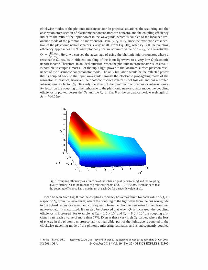
reasonableQc results in efficient coupling of the input lightwave to a very low-Qplasmonicnanoresonator. Therefore, in an ideal situation, when the photonic microresonator is lossless, itis possible to couple almost all of the input light power to the localized surface plasmon reso-nance of the plasmonic nanoresonator mode. The only limitation would be the reflected powerthat is coupled back to the input waveguide through the clockwise propagating mode of theresonator. In practice, however, the photonic microresonator is not lossless and has a limitedintrinsic quality factor,Q0. To study the effect of the photonic microresonator intrinsic qual-ity factor on the coupling of the lightwave to the plasmonic nanoresonator mode, the couplingefficiency is plotted versus theQ0 and theQc in Fig. 8 at the resonance peak wavelength ofλ0 = 764.65nm.
Fig. 8. Coupling efficiency as a function of the intrinsic quality factor (Q0) and the couplingquality factor (Qc) at the resonance peak wavelength ofλ0 = 764.65nm. It can be seen thatthe coupling efficiency has a maximum at eachQ0 for a specific value ofQc.
It can be seen from Fig. 8 that the coupling efficiency has a maximum for each value ofQ0 ata specificQc from the waveguide, where the coupling of the lightwave from the bus waveguideto the hybrid resonator system and consequently from the photonic resonator to the plasmonicnanoresonator is maximized. It can also be observed that whenQ0 is increased, the couplingefficiency is increased. For example, atQ0 = 1.5×10⁷ andQc = 8.6×10³ the coupling effi-ciency can reach a value of more than 77%. Even at these very highQ0 values, where the lossof energy in the photonic microresonator is negligible, part of the lightwave is coupled to theclockwise travelling mode of the photonic microring resonator, and is subsequently coupled
#151465 - $15.00 USD Received 22 Jul 2011; revised 18 Oct 2011; accepted 18 Oct 2011; published 24 Oct 2011(C) 2011 OSA 24 October 2011 / Vol. 19, No. 22 / OPTICS EXPRESS 22302

back to the bus waveguide as reflection. Achieving such high intrinsic quality factors is noteasily possible in practice with the current quality of materials and fabrication processes. Toinvestigate how practical is the proposed hybrid structure in efficiently coupling the lightwaveto the plasmonic nanoresonator mode, the optimization surface, presented in Fig. 8, is plotted inthe form of iso-|k|2 contours in Fig. 9. It can be seen for example that at aQ0 = 1.37×10⁵ andQc = 8.6×10³, the coupling efficiency is 73%, which still is large. The intrinsic quality factorof Q0 = 1.37×10⁵ and the coupling quality factor ofQc = 8.6×10³ are practically achievable.The proposed hybrid structure can also be extended to other photonic microresonator structuressuch as microdisk resonators, which have high quality factors. However, microdisk resonatorsusually have multiple radial modes, which makes the design more difficult. Other photonicmicroresonators such as microtoroids, microspheres, standing wave resonators, and photoniccrystal cavities [26,27] can also be used in the proposed architecture.
0.65
0.65
50.
660.
665
0.67
0.67
50.
680.
685
0.69
0.69
50.
70.
705
0.71
0.71
50.
720.
725
0.73
0.73
50.
740.
745
0.75
0.75
50.
76
Qc
Q0
0.76
0.76
30.
766
0.76
90.
770.77
30.
774
0.77
480.77
56
0.6 0.8 1 1.2 1.4 1.6
x 104
2
4
6
8
10
12
14
x 106
Fig. 9. Coupling efficiency as a function of the intrinsic quality factor,Q0, and the couplingquality factor,Qc at the resonance peak wavelength ofλ0 = 764.65nm. It can be seen thatthe coupling efficiency has a maximum at each intrinsic quality factor,Q0, for a specificcoupling quality factor,Qc.
It should be noted that the total energy that is coupled to the resonance mode of the plasmonicnanoresonator and results in large near-field enhancements is partly absorbed by the metallicnanoresonator, and is partly scattered. Depending on the application of interest, the plasmonicnanoresonator can be designed to have either a large absorption cross section or a large scatte-ring cross section. When a material is interacting with the enhanced near-field of the plasmonicnanoresonator, the energy can also be absorbed by the material. Here, we have demonstrated theresults for a gold nanorod. The plasmonic nanoresonator shape, size, and material can be usedto design different plasmonic nanoresonators with different absorption and scattering proper-ties. It should also be noted that we have optimized the coupling of the lightwave to the dipoleresonance mode of the plasmonic nanoresonator. The coupling efficiency can be optimized tohigher order resonance modes, as well.
The large coupling efficiency to a single plasmonic nanoresonator mode greatly improves thefield enhancement and signal-to-noise-ratio. This makes it possible to do practical individual
#151465 - $15.00 USD Received 22 Jul 2011; revised 18 Oct 2011; accepted 18 Oct 2011; published 24 Oct 2011(C) 2011 OSA 24 October 2011 / Vol. 19, No. 22 / OPTICS EXPRESS 22303

plasmonic nanoresonator sensing by using low input powers. Also, the proposed hybrid struc-ture can be realized on a chip, and is not alignment sensitive. Once the structure is implemented,excitation of the bus waveguide guarantees the excitation of the LSPR mode of the plasmonicnanoresonator. Also, the enhanced extinction of the hybrid resonator modes can be measured atthe output of the bus waveguide. This eliminates the need for a bulky microscope with precisealignment control and a very sensitive detector to interrogate single plasmonic nanoresonators.
In the proposed hybrid resonator structure, the photonic microresonator with a large intrinsicquality factor,Q0, facilitates the coupling of the lightwave from the bus waveguide to the plas-monic nanoresonator. In analogy to microwave antennas, the high-Q photonic microresonatorcan be considered as an impedance matching circuitry that optimizes the coupling of the inputpower to the plasmonic nanoresonator, which can be considered as a nanoantenna.
5. Conclusion
We have proposed, designed, and optimized a hybrid plasmonic-photonic resonator structureconsisting of a plasmonic nanoresonator and a photonic microresonator, which can be used toefficiently couple the lightwave to the LSPR mode of the plasmonic nanoresonator. We haveshown that by using the proposed hybrid structure, the coupling efficiency can be optimizedso that more than 73% of the lightwave is coupled to a single gold nanorod. This greatlyimproves the signal-to-noise-ratio and the field enhancements. The improved signal-to-noiseratio is critically important for interrogation of single plasmonic nanoresonators in applicationssuch as ultrasensitive sensing and spectroscopy. The on-chip and alignment-insensitive natureof the proposed structure makes it suitable for lab-on-chip applications, where a portable,low power, and compact device is desired. Also, since the broadband resonance signature ofthe plasmonic nanoresonator is enhanced by the photonic microresonator resonance modes,the extinction can be easily measured from the transmission spectrum. Therefore, to studythe resonance behavior of single plasmonic nanoresonators, the transmission spectrum of thebus waveguide can be used, alleviating the need for locating and measuring the scattering ofthe single nanoresonator. The proposed device is compact, and the hybrid resonator can beimplemented in a 40µm×40µm footprint. Therefore, many of them can be integrated on thesame chip for multianalyte sensing. Also, the proposed hybrid plasmonic-photonic structurecan employ the potentials of nanoplasmonic structures efficiently to bridge the gap betweenthe nano-scale world of electronics and the larger-scale world of photonics. Therefore, webelieve that our proposed hybrid platform can be used in different on-chip applications such aslab-on-chip sensing systems, on-chip spectroscopy, signal processing, and communications.
Acknowledgments
This work was supported by the Defense Advanced Research Projects Agency (DARPA) underContract HR 0011-10-1-0075 through the DARPA CIPHER Project (S. Rodgers). The authorswould like to thank Qing Li for helpful discussions.
#151465 - $15.00 USD Received 22 Jul 2011; revised 18 Oct 2011; accepted 18 Oct 2011; published 24 Oct 2011(C) 2011 OSA 24 October 2011 / Vol. 19, No. 22 / OPTICS EXPRESS 22304