hynix nand 128mo h27u1g8f2bt
TRANSCRIPT

This document is a general product description and is subject to change without notice. Hynix does not assume any responsibility for use of circuits described. No patent licenses are implied.Rev 1.2 / Dec. 2009 1
1
H27U1G8F2B Series1 Gbit (128 M x 8 bit) NAND Flash
1 Gb NAND FlashH27U1G8F2B

Rev 1.2 / Dec. 2009 2
1
H27U1G8F2B Series1 Gbit (128 M x 8 bit) NAND Flash
Document Title1 Gbit (128 M x 8 bit) NAND Flash Memory
Revision History
Revision No. History Draft Date Remark
0.0 Initial Draft. May. 13. 2008 Preliminary
0.1
1) Correct Table 5. Mode Selection.
Jul. 4. 2008 Preliminary
0.2
1) Correct Read ID 4th cycle value. (Table 15, Figure 19)
Aug. 19. 2008 Preliminary
1.0 1) Delete Preliminary Mar. 13. 2009
1.1 1) Insert FBGA Package Sep. 28. 2009
1.2 1) Correct fBGA PKG ball configuration Dec. 03. 2009
CLE ALE CE WE RE WP MODE
L L L H H X During Read (Busy)
↓ ↓ ↓
X X X H H X During Read (Busy)
4thCycle
4thCycle
15h → 1Dh

Rev 1.2 / Dec. 2009 3
1
H27U1G8F2B Series1 Gbit (128 M x 8 bit) NAND Flash
FEATURES SUMMARY
HIGH DENSITY NAND FLASH MEMORIES- Cost effective solutions for mass storage applications
NAND INTERFACE- x8 bus width.- Address / Data Multiplexing- Pinout compatiblity for all densities
SUPPLY VOLTAGE- 3.3 V device : Vcc = 2.7 V ~3.6 V
MEMORY CELL ARRAY- (2 K + 64) bytes x 64 pages x 1024 blocks
PAGE SIZE - (2 K + 64 spare) Bytes
BLOCK SIZE- (128 K + 4 K spare) Bytes
PAGE READ / PROGRAM- Random access : 25 us (max.)- Sequential access : 25 ns (min.)- Page program time : 200 us (typ.)
FAST BLOCK ERASE- Block erase time: 2 ms (Typ)
ELECTRONIC SIGNATURE- 1st cycle : Manufacturer Code- 2nd cycle : Device Code- 3rd cycle : Internal chip number, Cell Type, Number of Simultaneously Programmed Pages.- 4th cycle : Page size, Block size, Organization, Spare size
COPY BACK PROGRAM- Fast Data Copy without external buffering
CACHE READ- Internal buffer to improve the read throughput
CHIP ENABLE DON'T CARE- Simple interface with microcontroller
STATUS REGISTER- Normal Status Register (Read/Program/Erase)
HARDWARE DATA PROTECTION- Program/Erase locked during Power transitions.
DATA RETENTION- 100,000 Program/Erase cycles (with 1 bit / 528 byte ECC)- 10 years Data Retention
PACKAGE- H27U1G8F2BTR-BX : 48-Pin TSOP1 (12 x 20 x 1.2 mm) - H27U1G8F2BTR-BX (Lead & Halogen Free)- H27U1G8F2BFR-BX : 63-Ball FBGA (9 x 11 x 1.0 mm) - H27U1G8F2BFR-BX (Lead & Halogen Free)

Rev 1.2 / Dec. 2009 4
1
H27U1G8F2B Series1 Gbit (128 M x 8 bit) NAND Flash
1. SUMMARY DESCRIPTION
Hynix NAND H27U1G8F2B Series have 128 M x 8 bit with spare 4 M x 8 bit capacity. The device is offered in 3.3 V VccPower Supply, and with x8 I/O interface. Its NAND cell provides the most cost-effective solution for the solid state massstorage market. The memory is divided into blocks that can be erased independently so it is possible to preserve valid datawhile old data is erased.
The device contains 1024 blocks, composed by 64 pages. A program operation allows to write the 2112 byte page intypical 200 us and an erase operation can be performed in typical 2.0 ms on a 128 K byte block.
Data in the page can be read out at 25ns cycle time per byte. The I/O pins serve as the ports for address and data input/output as well as command input. This interface allows a reduced pin count and easy migration towards different densities,without any rearrangement of footprint.
Commands, Data and Addresses are synchronously introduced using CE, WE, RE, ALE and CLE input pin. The on-chipProgram/Erase Controller automates all program and erase functions including pulse repetition, where required, and inter-nal verification and margining of data. The modify operations can be locked using the WP input.
The chip supports CE don't care function. This function allows the direct download of the code from the NAND Flashmemory device by a microcontroller, since the CE transitions do not stop the read operation.
The output pin R/B (open drain buffer) signals the status of the device during each operation. In a system with multiplememories the R/B pins can be connected all together to provide a global status signal.
Even the write-intensive systems can take advantage of the H27U1G8F2B Series extended reliability of 100 K program/erase cycles by providing ECC (Error Correcting Code) with real time mapping-out algorithm.
The copy back function allows the optimization of defective blocks management: when a page program operation failsthe data can be directly programmed in another page inside the same array section without the time consuming serial datainsertion phase. Data read out after copy back read is allowed.
This device includes also extra features like OTP/Unique ID area, Read ID2 extension.The H27U1G8F2B is available in 48-TSOP1 12 x 20 mm and 63-FBGA 9 x 11 mm.
1.1 Product List
PART NUMBER ORGANIZATION Vcc RANGE PACKAGE
H27U1G8F2B x8 2.7V ~ 3.6V 48-TSOP1 / 63-FBGA

Rev 1.2 / Dec. 2009 5
1
H27U1G8F2B Series1 Gbit (128 M x 8 bit) NAND Flash
VCC
VSS
WP
CLE
ALE
RE
WE
CE IO0~IO7
R/B
NC
NC
NC NCNC
NC NC
NC
CLE
ALE Vss
VssVss
Vcc
Vcc
NC
NC
NC
WP
RE
CE WE RB
NC
NC
NC
NC
NC
NC
NC
NC
NC
NC
NC
NC
NC
NC
NC
NC
NC
I/O0
I/O1
I/O2 I/O3 I/O4
I/O5
I/O6
I/O7
NC NC
NC
NC NC NC
NC
PRE
NC
NC
NC
NCNC
NC NC
A
B
C
D
E
F
G
H
J
K
L
M
1 2 3 4 5 6 7 8 9 10
Figure 2 : 48-TSOP1 / 63-FBGA Contact, x8 Device
IO7 - IO0 Data Input / Outputs
CLE Command latch enable
ALE Address latch enable
CE Chip Enable
RE Read Enable
WE Write Enable
WP Write Protect
R/B Ready / Busy
Vcc Power Supply
Vss Ground
NC No Connection
Figure 1 : Logic Diagram Table 1 : Signal Names

Rev 1.2 / Dec. 2009 6
1
H27U1G8F2B Series1 Gbit (128 M x 8 bit) NAND Flash
1.2 PIN DESCRIPTION
Table 2 : Pin Description
NOTE :
1. A 0.1uF capacitor should be connected between the Vcc Supply Voltage pin and the Vss Ground pin to decouple thecurrent surges from the power supply. The PCB track widths must be sufficient to carry the currents required duringprogram and erase operations.
Pin Name Description
IO0 ~ IO7
DATA INPUTS/OUTPUTSThe IO pins allow to input command, address and data and to output data during read / programoperations. The inputs are latched on the rising edge of Write Enable (WE). The I/O buffer float toHigh-Z when the device is deselected or the outputs are disabled.
CLECOMMAND LATCH ENABLEThis input activates the latching of the IO inputs inside the Command Register on the Rising edge ofWrite Enable (WE).
ALEADDRESS LATCH ENABLEThis input activates the latching of the IO inputs inside the Address Register on the Rising edge ofWrite Enable (WE).
CE CHIP ENABLEThis input controls the selection of the device.
WEWRITE ENABLEThis input acts as clock to latch Command, Address and Data. The IO inputs are latched on the riseedge of WE.
RE
READ ENABLEThe RE input is the serial data-out control, and when active drives the data onto the I/O bus. Data isvalid tREA after the falling edge of RE which also increments the internal column address counter byone.
WPWRITE PROTECTThe WP pin, when Low, provides an Hardware protection against undesired modify (program / erase)operations.
R/B READY BUSYThe Ready/Busy output is an Open Drain pin that signals the state of the memory.
Vcc SUPPLY VOLTAGEThe Vcc supplies the power for all the operations (Read, Write, Erase).
Vss GROUND
NC NO CONNECTION

Rev 1.2 / Dec. 2009 7
1
H27U1G8F2B Series1 Gbit (128 M x 8 bit) NAND Flash
Figure 3 : Array Organization
Table 3 : Address Cycle MapNOTE:
1. L must be set to Low.2. 1st & 2nd cycle are Column Address.3. 3rd to 4th cycle are Row Address.
IO0 IO1 IO2 IO3 IO4 IO5 IO6 IO7
1st Cycle A0 A1 A2 A3 A4 A5 A6 A7
2nd Cycle A8 A9 A10 A11 L(1) L(1) L(1) L(1)
3rd Cycle A12 A13 A14 A15 A16 A17 A18 A19
4th Cycle A20 A21 A22 A23 A24 A25 A26 A27
Plane
2 K Bytes 64 Bytes
I/O0 ~ 7
1 Page = (2 K + 64) Bytes
1 Block = (2 K + 64) Bytes x 64 pages
= (128 K + 4 K) Bytes
1 Device = (128 K + 4 K) Bytes x 1024 Block
Page Buffer
1024 Blocks
per Plane
1023
1024
1
0
.
.
.

Rev 1.2 / Dec. 2009 8
1
H27U1G8F2B Series1 Gbit (128 M x 8 bit) NAND Flash
Table 4 : Command Set
NOTE : With the CE don't care option CE high during latency time does not stop the read operation
Table 5 : Mode Selection
FUNCTION 1st 2nd 3rd 4thAcceptable Command
During Busy
PAGE READ 00h 30h - -
READ FOR COPY-BACK 00h 35h - -
READ ID 90h - - -
RESET FFh - - - Yes
PAGE PROGRAM 80h 10h - -
COPY BACK PGM 85h 10h - -
BLOCK ERASE 60h D0h - -
READ STATUS REGISTER 70h - - - Yes
RANDOM DATA INPUT 85h - - -
RANDOM DATA OUTPUT 05h E0h - -
CACHE READ START 31h - -
CACHE READ EXIT 3Fh - - -
CLE ALE CE WE RE WP MODE
H L L Rising H XRead Mode
Command Input
L H L Rising H X Address Input (4 cycles)
H L L Rising H HWrite Mode
Command Input
L H L Rising H H Address Input (4 cycles)
L L L Rising H H Data Input
L L L H Falling X Data Output
X X X H H X During Read (Busy)
X X X X X H During Program (Busy)
X X X X X H During Erase (Busy)
X X X X X L Write Protect
X X H X X 0 V / Vcc Stand By

Rev 1.2 / Dec. 2009 9
1
H27U1G8F2B Series1 Gbit (128 M x 8 bit) NAND Flash
2. BUS OPERATION
There are six standard bus operations that control the device. These are Command Input, Address Input, Data Input,Data Output, Write Protect, and Standby.
Typically glitches less than 5 ns on Chip Enable, Write Enable and Read Enable are ignored by the memory and do notaffect bus operations.
2.1 Command Input. Command Input bus operation is used to give a command to the memory device. Command are accepted with Chip En-
able low, Command Latch Enable High, Address Latch Enable low and Read Enable High and latched on the rising edge ofWrite Enable. Moreover for commands that starts a modify operation (write/erase) the Write Protect pin must be high. SeeFigure 5 and Table 12 for details of the timings requirements.
2.2 Address Input. Address Input bus operation allows the insertion of the memory address. To insert the 28 addresses needed to access
the 1Gbit 4 clock cycles are needed. Addresses are accepted with Chip Enable low, Address Latch Enable High, CommandLatch Enable low and Read Enable High and latched on the rising edge of Write Enable. Moreover for commands that startsa modify operation (write/erase) the Write Protect pin must be high. See Figure 6 and Table 12 for details of the timingsrequirements.
2.3 Data Input. Data Input bus operation allows to feed to the device the data to be programmed. The data insertion is serially and timed
by the Write Enable cycles. Data are accepted only with Chip Enable low, Address Latch Enable low, Command Latch Enablelow, Read Enable High, and Write Protect High and latched on the rising edge of Write Enable. See Figure 7 and Table 12for details of the timings requirements.
2.4 Data Output. Data Output bus operation allows to read data from the memory array and to check the status register content, the lock
status and the ID data. Data can be serially shifted out toggling the Read Enable pin with Chip Enable low, Write EnableHigh, Address Latch Enable low, and Command Latch Enable low. See Figure 8, 9, 10 and Table 12 for details of the timingsrequirements.
2.5 Write Protect. Hardware Write Protection is activated when the Write Protect pin is low. In this condition modify operation do not start
and the content of the memory is not altered. Write Protect pin is not latched by Write Enable to ensure the protectioneven during the power up.
2.6 Standby. In Standby the device is deselected, outputs are disabled and Power Consumption reduced.

Rev 1.2 / Dec. 2009 10
1
H27U1G8F2B Series1 Gbit (128 M x 8 bit) NAND Flash
3. DEVICE OPERATION
3.1 Page Read.Upon initial device power up, the device defaults to Read mode. This operation is also initiated by writing 00h and 30h
to the command register along with four address cycles. In two consecutive read operations, the second one does need00h command, which four address cycles and 30h command initiates that operation. Second read operation always re-quires setup command if first read operation was executed using also random data out command.
Two types of operations are available: random read , serial page read. The random read mode is enabled when the pageaddress is changed. The 2112 bytes of data within the selected page are transferred to the data registers in less than 25us(tR). The system controller may detect the completion of this data transfer (tR) by analyzing the output of R/B pin. Oncethe data in a page is loaded into the data registers, they may be read out in 25 ns cycle time by sequentially pulsing RE.The repetitive high to low transitions of the RE clock make the device output the data starting from the selected columnaddress up to the last column address.
The device may output random data in a page instead of the consecutive sequential data by writing random data outputcommand.
The column address of next data, which is going to be out, may be changed to the address which follows random dataoutput command.
Random data output can be operated multiple times regardless of how many times it is done in a page.After power up, device is in read mode so 00h command cycle is not necessary to start a read operation.Any operation other than read or random data output causes device to exit read mode.Check Figure 11, Figure 12, and Figure 13 as references.
3.2 Page Program.The device is programmed basically by page, but it does allow multiple partial page programming of a word or consec-
utive bytes up to 2112, in a single page program cycle. The number of consecutive partial page programming operationwithin the same page without an intervening erase operation must not exceed 8; for example, 4 times for main array(1time/512byte) and 4 times for spare array (1time/16byte).
A page program cycle consists of a serial data loading period in which up to 2112 bytes of data may be loaded into thedata register, followed by a non-volatile programming period where the loaded data is programmed into the appropriatecell.
The serial data loading period begins by inputting the Serial Data Input command (80h), followed by the four cycle ad-dress inputs and then serial data. The words other than those to be programmed do not need to be loaded. The devicesupports random data input in a page. The column address of next data, which will be entered, may be changed to theaddress which follows random data input command (85h). Random data input may be operated multiple times regardlessof how many times it is done in a page.
The Page Program confirm command (10h) initiates the programming process. Writing 10h alone without previously en-tering the serial data will not initiate the programming process. The internal write state controller automatically executesthe algorithms and timings necessary for program and verify, thereby freeing the system controller for other tasks. Oncethe program process starts, the Read Status Register command may be entered to read the status register. The systemcontroller can detect the completion of a program cycle by monitoring the R/B output, or the Status bit (I/O 6) of the StatusRegister. Only the Read Status command and Reset command are valid while programming is in progress. When the PageProgram is complete, the Write Status Bit (I/O 0) may be checked. The internal write verify detects only errors for "1"sthat are not successfully programmed to "0"s. The command register remains in Read Status command mode until anothervalid command is written to the command register. Figure 14 and Figure 15 detail the sequence.

Rev 1.2 / Dec. 2009 11
1
H27U1G8F2B Series1 Gbit (128 M x 8 bit) NAND Flash
3.3 Block Erase.The Erase operation is done on a block basis. Block address loading is accomplished in two cycles initiated by an Erase
Setup command (60h). Only address A18 to A27 is valid while A12 to A17 are ignored. The Erase Confirm command (D0h)following the block address loading initiates the internal erasing process. This two-step sequence of setup followed by ex-ecution command ensures that memory contents are not accidentally erased due to external noise conditions.
At the rising edge of WE after the erase confirm command input, the internal write controller handles erase and erase-verify.
Once the erase process starts, the Read Status Register command may be entered to read the status register. The systemcontroller can detect the completion of an erase by monitoring the R/B output, or the Status bit (I/O 6) of the Status Reg-ister. Only the Read Status command and Reset command are valid while erasing is in progress. When the erase operationis completed, the Write Status Bit (I/O 0) may be checked.
Figure 18 details the sequence.
3.4 Copy-Back Program.The copy-back program is configured to quickly and efficiently rewrite data stored in one page without utilizing an ex-
ternal memory. Since the time-consuming cycles of serial access and re-loading cycles are removed, the system perform-ance is improved. The benefit is especially obvious when a portion of a block is updated and the rest of the block is alsoneeded to be copied to the newly assigned free block. The operation for performing a copy-back program is a sequentialexecution of page-read without serial access and copying-program with the address of destination page. A read operationwith "35h" command and the address of the source page moves the whole 2112byte data into the internal data buffer. Assoon as the device returns to Ready state, optional data read-out is allowed by toggling RE, or Copy Back command (85h)with the address cycles of destination page may be written. The Program Confirm command (10h) is required to actuallybegin the programming operation. Data input cycle for modifying a portion or multiple distant portions of the source pageis allowed as shown in Figure 17.
"When there is a program-failure at Copy-Back operation, error is reported by pass/fail status. But, if Copy-Back opera-tions are accumulated over time, bit error due to charge loss is not checked by external error detection/correction scheme.For this reason, two bit error correction is recommended for the use of Copy-Back operation."
Figure 16 and Figure 17 show the command sequence for the copy-back operation.Please note that WP value is don't care during Read for copy back, while it must be set to Vcc when performing the
program .
3.5 Read Status Register.The device contains a Status Register which may be read to find out whether read, program or erase operation is com-
pleted, and whether the program or erase operation is completed successfully. After writing 70h command to the commandregister, a read cycle outputs the content of the Status Register to the I/O pins on the falling edge of CE or RE, whicheveroccurs last. This two line control allows the system to poll the progress of each device in multiple memory connectionseven when R/B pins are common-wired. RE or CE does not need to be toggled for updated status. Refer to Table 13 forspecific Status Register definitions, and Figure 10 for specific timings requirements. The command register remains in Sta-tus Read mode until further commands are issued to it. Therefore, if the status register is read during a random read cycle,the read command (00h) should be given before starting read cycles.
3.6 Read ID.The device contains a product identification mode, initiated by writing 90h to the command register, followed by an ad-
dress input of 00h. Four read cycles sequentially output the manufacturer code (ADh), and the device code and 00h, 4thcycle ID, respectively. The command register remains in Read ID mode until further commands are issued to it. Figure 19shows the operation sequence, while Table 14 to Table 17 explain the byte meaning.

Rev 1.2 / Dec. 2009 12
1
H27U1G8F2B Series1 Gbit (128 M x 8 bit) NAND Flash
3.7 Reset.The device offers a reset feature, executed by writing FFh to the command register. When the device is in Busy state
during random read, program or erase mode, the reset operation will abort these operations. The contents of memory cellsbeing altered are no longer valid, as the data will be partially programmed or erased. The command register is cleared towait for the next command, and the Status Register is cleared to value E0h when WP is high. Refer to Table 13 for devicestatus after reset operation. If the device is already in reset state a new reset command will not be accepted by the com-mand register. The R/B pin transitions to low for tRST after the Reset command is written (see Figure 20).
3.8 Read CacheThe Read Cache function permits a page to be read from the page register while another page is simultaneously read
from the Flash array. A Read Page command, as defined in 3.1, shall be issued prior to the initial sequential or randomRead Cache command in a read cache sequence.
The Read Cache function may be issued after the Read function is complete (SR[6] is set to one). The host may enterthe address of the next page to be read from the Flash array. Data output always begins at column address 00h. If thehost does not enter an address to retrieve, the next sequential page is read. When the Read Cache function is issued, SR[6]is cleared to zero (busy). After the operation is begun SR[6] is set to one (ready) and the host may begin to read the datafrom the previous Read or Read Cache function. Issuing an additional Read Cache function copies the data most recentlyread from the array into the page register. When no more pages are to be read, the final page is copied into the pageregister by issuing the 3Fh command. The host may begin to read data from the page register when SR[6]is set to one(ready). When the 31h and 3Fh commands are issued, SR[6] shall be cleared to zero (busy) until the page has finishedbeing copied from the Flash array.
The host shall not issue a sequential Read Cache (31h) command after the last page of the device is read. Figure 21 defines the Read Cache behavior and timings for the beginning of the cache operations subsequent to a Read
command being issued. SR[6] conveys whether the next selected page can be read from the page register. Figure 21also shows the Read Cache behavior and timings for the end of cache operation.

Rev 1.2 / Dec. 2009 13
1
H27U1G8F2B Series1 Gbit (128 M x 8 bit) NAND Flash
4. OTHER FEATURES
4.1 Data Protection.The device is designed to offer protection from any involuntary program/erase during power-transitions. An internal volt-
age detector disables all functions whenever Vcc is below about 1.8 V (3.3 V version). WP pin provides hardware protectionand is recommended to be kept at VIL during power-up and power-down. A recovery time of minimum 10us is requiredbefore internal circuit gets ready for any command sequences as shown in Figure 22. The two-step command sequencefor program/erase provides additional software protection.
4.2 Ready/Busy.The device has a Ready/Busy output that provides method of indicating the completion of a page program, erase, copy-
back, cache program and random read completion. The R/B pin is normally high and goes to low when the device is busy(after a reset, read, program, erase operation). It returns to high when the internal controller has finished the operation.The pin is an open-drain driver thereby allowing two or more R/B outputs to be Or-tied. Because pull-up resistor value isrelated to tr(R/B) and current drain during busy (I busy), an appropriate value can be obtained with the following referencechart (Figure 23). Its value can be determined by the following guidance.

Rev 1.2 / Dec. 2009 14
1
H27U1G8F2B Series1 Gbit (128 M x 8 bit) NAND Flash
Table 6 : Number of Valid Blocks
NOTE:1. The 1st block is guaranteed to be a valid block at the time of shipment.
Table 7 : Absulute maximum ratings
NOTE: 1. Except for the rating "Operating Temperature Range", stresses above those listed in the Table "Absolute MaximumRatings" may cause permanent damage to the device. These are stress ratings only and operation of the device at theseor any other conditions above those indicated in the Operating sections of this specification is not implied. Exposure toAbsolute Maximum Rating conditions for extended periods may affect device reliability. Refer also to the HYNIX SUREProgram and other relevant quality documents.
2. Minimum Voltage may undershoot to -2V during transition and for less than 20ns during transitions.
Parameter Symbol Min Typ Max Unit
Valid Block Number NVB 1004 1024 Blocks
Symbol Parameter Value Unit
TAAmbient Operating Temperature (Temperature Range Option 1) 0 to 70 °C
Ambient Operating Temperature (Temperature Range Option 6) – 40 to 85 °C
TBIAS Temperature Under Bias – 50 to 125 °C
TSTG Storage Temperature – 65 to 150 °C
VIO (2) Input or Output Voltage – 0.6 to 4.6 V
VCC Supply Voltage – 0.6 to 4.6 V

Rev 1.2 / Dec. 2009 15
1
H27U1G8F2B Series1 Gbit (128 M x 8 bit) NAND Flash
Figure 4 : Block Diagram
ADDRESS REGISTER/COUNTER
PROGRAM ERASE
CONTROLLER HV GENERATION
COMMAND INTERFACE
LOGIC
COMMAND REGISTER
DATA REGISTER
IO
RE
BUFFERS
Y DECODER
PAGE BUFFER
X
DEC ODER
1024 Mbit + 32 Mbit
NAND Flash
MEMORY ARRAY
WP
CE
WE
CLE
ALE
A27 ~ A0

Rev 1.2 / Dec. 2009 16
1
H27U1G8F2B Series1 Gbit (128 M x 8 bit) NAND Flash
Table 8 : DC and Opeating Characteristics
Table 9 : AC Test Conditions
Parameter Symbol Test Conditions3.3 Volt
UnitMin Typ Max
Operating Current
Sequential Read
ICC1 tRC = 25 ns, CE = VIL, IOUT = 0 mA - 15 30 mA
Program ICC2 - - 15 30 mA
Erase ICC3 - - 15 30 mA
Stand-by Current (TTL) ICC4CE = VIH, WP = 0 V/VCC
1 mA
Stand-By Current (CMOS) ICC5 CE = VCC-0.2, WP = 0/VCC 10 50 uA
Input Leakage Current ILI VIN = 0 to Vc (max) - ±10 uA
Output Leakage Current ILO VOUT = 0 to Vcc(max) - ±10 uA
Input High Voltage VIH - 0.8 x VCC - VCC + 0.3 V
Input Low Voltage VIL - -0.3 - 0.2 x VCC V
Output High Voltage Level VOH IOH = - 400 uA 2.4 - - V
Outpul Low Voltage Level VOL IOL = 2.1 mA - - 0.4 V
Output Low Current (R/B) IOL (R/B) VOL= 0.4 V 8 10 - mA
Vcc supply voltage (erase and program) lockout
VLKO - 1.8 - V
ParameterValue
3.3 Volt
Input Pulse Levels 0 V to VCC
Input Rise and Fall Times 5 ns
Input and Output Timing Levels VCC / 2
Output Load (1.65V – 1.95V & 2.5V - 3.6V) 1 TTL GATE and CL = 50 pF

Rev 1.2 / Dec. 2009 17
1
H27U1G8F2B Series1 Gbit (128 M x 8 bit) NAND Flash
Table 10 : Pin Capacitance (TA = 25 ℃, f = 1.0 MHz)
Table 11 : Program / Erase Characteristics
NOTE : Typical program time is defined as the time when which more than 50 % of the whole pages are programmed at Vcc = 3.3 V and 25 ℃.
Item Symbol Test Condition Min Max Unit
Input / Output Capacitance CI/O VIL = 0V - 10 pF
Input Capacitance CIN VIN = 0V - 10 pF
Parameter Symbol Min Typ Max Unit
Program Time tPROG - 200 700 us
Dummy Busy Time for Cache Program tCBSY - 3 700 us
Dummy Busy Time for the Lock or Lock-tight Block tLBSY - 5 10 us
Number of partial Program Cycles in the same page Nop - - 8 Cycle
Block Erase Time tBERS - 2 3 ms

Rev 1.2 / Dec. 2009 18
1
H27U1G8F2B Series1 Gbit (128 M x 8 bit) NAND Flash
Table 12 : AC Timing CharacteristicsNOTE :1) If Reset Command (FFh) is written at Ready State, the device goes into Busy for maximum 5 us
Parameter Symbol3.3 Volt
UnitMin Max
CLE Setup time tCLS 12 ns
CLE Hold time tCLH 5 ns
CE Setup time tCS 20 ns
CE Hold time tCH 5 ns
WE Pulse width tWP 12 ns
ALE Setup time tALS 12 ns
ALE Hold time tALH 5 ns
Data Setup time tDS 12 ns
Data Hold time tDH 5 ns
Write Cycle time tWC 25 ns
WE High Hold time tWH 10 ns
Address to Data Loading time tADL 70 ns
Data Transfer from Cell to Register tR 25 us
ALE to RE Delay tAR 10 ns
CLE to RE Delay tCLR 10 ns
Ready to RE Low tRR 20 ns
RE Pulse Width tRP 12 ns
WE High to Busy tWB 100 ns
Read Cycle Time tRC 25 ns
RE Access Time tREA 20 ns
RE High to Output Hi-Z tRHZ 100 ns
CE High to Output Hi-Z tCHZ 30 ns
CE High to ALE or CLE Don’t care tCSD 10 ns
RE High to Output Hold tRHOH 15 ns
RE Low to Output Hold tRLOH 5 ns
CE High to Output Hold tCOH 15 ns
RE High Hold Time tREH 10 ns
Output Hi-Z to RE Low tIR 0 ns
RE High to WE Low tRHW 100 ns
WE High to RE Low tWHR 60 ns
Device Resetting Time (Read/Program/Erase) tRST 5/10/500 1) us

Rev 1.2 / Dec. 2009 19
1
H27U1G8F2B Series1 Gbit (128 M x 8 bit) NAND Flash
Table 13 : Status Register Coding
Table 14 : Device Identifier Coding
Table 15 : Read ID Data Table
IO Page Program Block Erase Read CacheRead CODING
0 Pass / Fail Pass / Fail NA NA Pass: ‘0’ Fail: ‘1’
1 NA NA NA NA -
2 NA NA NA NA -
3 NA NA NA NA -
4 NA NA NA NA -
5 Ready/Busy Ready/Busy Ready/Busy P/E/R Controller Bit Active: ‘0’ Idle:’1’
6 Ready/Busy Ready/Busy Ready/Busy Ready/Busy Busy: ‘0’ Ready:’1’
7 Write Protect Write Protect Write Protect NA Protected: ‘0’ Not Protected: ‘1’
DEVICE IDENTIFIER BYTE DESCRIPTION
1st Manufacturer Code
2nd Device Identifier
3rd Internal Chip Number, Cell Type, etc.
4th Page Size, Block Size, Spare Size, Organization
Part Number Voltage Bus Width
1st cycle(Manufacture Code)
2nd cycle(Device Code)
3rd cycle
4th cycle
H27U1G8F2B 3.3V x8 ADh F1h 00h 1Dh

Rev 1.2 / Dec. 2009 20
1
H27U1G8F2B Series1 Gbit (128 M x 8 bit) NAND Flash
Table 16 : 3rd Byte of Device Identifier Description
Table 17 : 4th Byte of Device Identifier Description
Description IO7 IO6 IO5 IO4 IO3 IO2 IO1 IO0
Die / Package
1248
0 00 11 01 1
Cell Type
2 Level Cell4 Level Cell8 Level Cell16 Level Cell
0 00 11 01 1
Number ofSimultaneously
Programmed Pages
1248
0 00 11 01 1
Interleave ProgramBetween multiple chips
Not Supported
01
Write Cache NotSupported
01
Description IO7 IO6 IO5-4 IO3 IO2 IO1-0
Page Size(Without Spare Area)
1KB2KB4KB8KB
0 00 11 01 1
Spare Area Size(Byte / 512Byte)
816
01
Serial Access Time
45 ns25 nsReservedReserved
0011
0101
Block Size(Without Spare Area)
64K128K256K512KB
0 00 11 01 1
Organization X8X16
01

Rev 1.2 / Dec. 2009 21
1
H27U1G8F2B Series1 Gbit (128 M x 8 bit) NAND Flash
Figure 5 : Command Latch Cycle
Figure 6 : Address Latch Cycle
tCLS
tCS
tWC
tALS tALS tALS tALS tALHtALHtALHtALH
tWC tWC
tWP tWP
tWH
tWP tWP
tWH tWH
tDS
Col.Add1
CLE
CE
WE
ALE
I/Ox Col.Add2 Row Add1 Row Add2
tDS tDS tDS
tDHtDHtDHtDH

Rev 1.2 / Dec. 2009 22
1
H27U1G8F2B Series1 Gbit (128 M x 8 bit) NAND Flash
Figure 7 : Input Data Latch Cycle
Figure 8 : Sequential Out Cycle after Read (CLE=L, WE=H, ALE=L)
tRC
CE
RE
I/Ox
R/B
tREA
tRR
Dout Dout Dout
Notes: Transition is measured at +/-200mV from steady state voltage with load. This parameter is sampled and not 100% tested. (tCHZ, tRHZ) tRHOH starts to be valid when frequency is lower than 33 MHz. tRLOH is valid when frequency is higher than 33 MHz.
tREA
tRHZ tRHZ
tREA
tCHZ
tCOH
tRHOH
tREH
tWC
tCLH
tCH
tWP
tWH
DIN 1 DIN 0 DIN final
tWH tDH tDH tDH
tDS tDS tDS
tWP tWP
CLE
ALE
CE
I/Ox
WE
tALS

Rev 1.2 / Dec. 2009 23
1
H27U1G8F2B Series1 Gbit (128 M x 8 bit) NAND Flash
Figure 9 : Sequential Out Cycle after Read
Figure 10 : Status Read Cycle

Rev 1.2 / Dec. 2009 24
1
H27U1G8F2B Series1 Gbit (128 M x 8 bit) NAND Flash
Figure 11 : Read Operation (Read One Page)
Figure 12 : Read Operation Intercepted by CE
CLE
ALE
CE
I/Ox
WE
RE
R/D
tWC
tCLR
tRR
00h 30hCol.Add1
Column Address Row Address
Col.Add2 Row Add1 Row Add2
Busy
Dout N Dout N+ Dout M
tWB
tAR
tR tRCtRHZ
tWB
tAR
tCHZ
tCOH
tRCtR
tRR
Busy
00h 30hDout
NDoutN+1
DoutN+2
Col. Add1
Col. Add2
Row Add1
Row Add2
Column Address Row Address
CLE
CE
WE
ALE
RE
I/Ox
R/B

Rev 1.2 / Dec. 2009 25
1
H27U1G8F2B Series1 Gbit (128 M x 8 bit) NAND Flash
Figure 13 : Random Data Output
CLE
ALE
CE
RE
R/B
I/Ox
WE
tCLR
00h
Colu
mn A
ddre
ss
Row
Addre
ss
Busy
30h
05h
E0h
Dou
t N
Dou
t M
Dout
N+1
Dout
M+1
Col.
Add1
Row
Add1
Row
Add2
Col.
Add2
Colu
mn A
ddre
ss
Col.
Add1
Col.
Add2
tRtR
C
tWB
tAR tRR
tWH
R
tREA
tRH
W

Rev 1.2 / Dec. 2009 26
1
H27U1G8F2B Series1 Gbit (128 M x 8 bit) NAND Flash
Figure 14 : Page Program Opeation
CLE
ALE
CE
RE
R/B
I/Ox
WE
tWC
80hCol.
Add1
Serial Data Input Command
Column Address
NOTES : tADL is the time from the WE rising edge of final address cycle to the WE rising edge of first data cycle.
Row AddressRead StatusCommand
ProgramCommand
I/O0=0 Successful ProgramI/O0=1 Error in Program
1 up to m ByteSerial Input
Col.Add2
RowAdd1
RowAdd2
DinN
DinM 10h 70h I/O
tWC
tWB tPROG tWHR
tWC
tADL

Rev 1.2 / Dec. 2009 27
1
H27U1G8F2B Series1 Gbit (128 M x 8 bit) NAND Flash
Figure 15 : Random Data In
CLE
ALE
CE
RE
R/B
I/Ox
WE
tWC
80h
Din N
Din M
Din J
Din K
85h
10h
70h
I
/OCo
l. Ad
d1Co
l. Ad
d2Co
l. Ad
d1Co
l. Ad
d2Rw
o Ad
d1Rw
o Ad
d2
tWC
tWB
tWH
RtP
RO
G
Ser
ial D
ata
Input
Com
man
dRan
dom
Dat
aIn
put
Com
man
dCol
um
n A
ddre
ssCol
um
n A
ddre
ssRow
Addre
ss
NO
TES :
1. tA
DL
is t
he
tim
e fr
om t
he
WE r
isin
g e
dge
of f
inal
addre
ss c
ycle
to
the
WE r
sing e
dge
of f
irst
dat
a cy
cle.
Ser
ial I
nput
Ser
ial I
nput
Pro
gra
mCom
man
d
Rea
d S
tatu
sCom
man
d
tWC
tAD
LtA
DL

Rev 1.2 / Dec. 2009 28
1
H27U1G8F2B Series1 Gbit (128 M x 8 bit) NAND Flash
Figure 16 : Copy Back Read with Optional Data Readout
CLE
ALE
CE
RE
R/B
I/Ox
WE
tCLR
00h
Colu
mn A
ddre
ss
Row
Addre
ss
Busy
35h
05h
E0h
Dou
t N
Dou
t M
Dout
N+1
Dout
M+1
Col.
Add1
Row
Add1
Row
Add2
Col.
Add2
Colu
mn A
ddre
ss
Col.
Add1
Col.
Add2
tRtR
C
tWB
tAR tRR
tWH
R
tREA
tRH
W

Rev 1.2 / Dec. 2009 29
1
H27U1G8F2B Series1 Gbit (128 M x 8 bit) NAND Flash
Figure 17 : Copy Back Program with Random Data Input
CLE
CE
WE
tWC
tWB
tRtR
C
tAD
L
tPR
OG
tWH
R
tWB
ALE
RE
00h
35h
10h
I/O70
h85
hD
ata
Data
Da
taD
ata
85
hD
ata
Da
ta
Bus
y
NO
TE
S: 1
. tA
DL
is th
e tim
e fr
om th
e W
E r
isin
g ed
ge o
f fin
al a
ddre
ss c
ycle
to th
e W
E r
isin
g ed
ge o
f firs
t dat
a cy
cle.
Col
umn
Add
ress
Col
umn
Add
ress
Dat
a O
utD
ata
InR
ow A
ddre
ssR
ow A
ddre
ssR
eal S
tatu
s C
omm
and
Bus
y
IO0=
0 S
uces
sful
Pro
gram
IO0=
1 E
rror
in P
rogr
amC
opy
Bac
k D
ata
Inpu
t Com
man
d
Col
Add1
Row
Add1
Row
Add2
Col
Add2
Col
Add1
Row
Add1
Row
Add2
Col
Add2
Col
umn
Add
ress
Col
Add1
Col
Add2
I/Ox
R/B
R/B
tRtP
RO
G
I/O7~
000
h35
h
Col
add
1,2
& R
ow a
dd 1
,2C
ol a
dd 1
,2 &
Row
add
1,2
Col
add
1,2
85h
85h
10h
I/Ox
70h
addr
ess
addr
ess
addr
ess
Dat
a ou
tD
ata
InD
ata
In

Rev 1.2 / Dec. 2009 30
1
H27U1G8F2B Series1 Gbit (128 M x 8 bit) NAND Flash
Figure 18 : Block Erase Operation (Erase One Block)
Figure 19 : Read ID Operation
90h
CLE
CE
WE
ALE
RE
I/O x 00h
tREA
Read ID Command Address 1 cycle Maker Code Device Code
ADh
4th Cycle 3rd Cycle
F1h 1Dh00h
tAR
tWC
CLE
CE
WE
ALE
RE
I/Ox
R/B
tWB tBERS
BUSY
70h I/O0Row Add1 Row Add360h
Auto Block Erase Setup Command Erase Confirm Command
Read StatusCommand
I/O0=0 Successful EraseI/O0=1 Error in Erase
Block Address
D0h

Rev 1.2 / Dec. 2009 31
1
H27U1G8F2B Series1 Gbit (128 M x 8 bit) NAND Flash
Figure 20 : Reset Operation Timing
FFh
tRST
WE
ALE
CLE
RE
IO7:0
R/B

Rev 1.2 / Dec. 2009 32
1
H27U1G8F2B Series1 Gbit (128 M x 8 bit) NAND Flash
Figure 21 : Read Operation with Read Cache
00h
ALE
CE
CLE
WE
RE
R/B
I/Ox
tRBSY tRBSY tRBSY
tRBSY
30h Col.
Add1
Col.
Add2Row.
Add1
Row.
Add231h
31h31h
Data Cache
Page Buffer
Cell Array
31h
A
Dout N Dout M
Dout M
Dout N+
Dout N Dout N+ 3FhDout M Dout N Dout N+ Dout M Dout N Dout N+
tR
A
ALE
CE
CLE
WE
RE
R/B
I/Ox
1
1
1
4 5 6 7 8 9
2 3
2
3
3
Page N
Page N
Page N
Page N + 1
4
5
5
Page N + 1
Page N + 1
Page N + 2
6
7
7
Page N + 2
Page N + 2
Page N + 3
8 9
Page N + 3
Page N + 3

Rev 1.2 / Dec. 2009 33
1
H27U1G8F2B Series1 Gbit (128 M x 8 bit) NAND Flash
Figure 22 : Power on and Data Protection timings
10 us
2.5 V (Vth)
Vcc
WE
WP

Rev 1.2 / Dec. 2009 34
1
H27U1G8F2B Series1 Gbit (128 M x 8 bit) NAND Flash
Figure 23 : Ready/Busy Pin Electrical Specifications
Rp value guidence
Rp (min) = =
where IL is the sum of the input currnts of all devices tied to the R/B pin.
Rp(max) is determined by maximum permissible limit of tr
@ Vcc = 3.3 V, Ta = 25°C, CL=50pF
Fig. Rp vs tr, tf & Rp vs ibusy
Vcc (Max.) - VOL (Max.) 3.2V
LIOL + L
Rp ibusy
Rp (ohm)
ibusy
ibusy
[A]
tr, tf
[s
]
tf
2.4 200
1501.2
50
1000.8
0.6
1.8 1.8 1.8 1.8
Busy
Ready Vcc
VOH
trtf
VOL
VOL : 0.4V, VOH : 2.4V
Vcc
300n 3m
1k 2k 3k 4k
200n 2m
100n 1m
GND
Device
open drain output
R/B
tR

Rev 1.2 / Dec. 2009 35
1
H27U1G8F2B Series1 Gbit (128 M x 8 bit) NAND Flash
Bad Block ManagementDevices with Bad Blocks have the same quality level and the same AC and DC characteristics as devices where all the
blocks are valid. A Bad Block does not affect the performance of valid blocks because it is isolated from the bit line andcommon source line by a select transistor. The devices are supplied with all the locations inside valid blocks erased(FFh).The Bad Block Information is written prior to shipping. Any block where the 1st Byte in the spare area of the 1st or 2nd thpage (if the 1st page is Bad) does not contain FFh is a Bad Block. The Bad Block Information must be read before anyerase is attempted as the Bad Block Information may be erased. For the system to be able to recognize the Bad Blocksbased on the original information it is recommended to create a Bad Block table following the flowchart shown in Figure24. The 1st block, which is placed on 00h block address is guaranteed to be a valid block.
Figure 24 : Bad Block Management Flowchart
NOTE :- Make sure that either the 1st or 2nd page of every initial block has not FFh data at the column address of 2048.
Rev 1.2 / Dec. 2009 36
1
H27U1G8F2B Series1 Gbit (128 M x 8 bit) NAND Flash
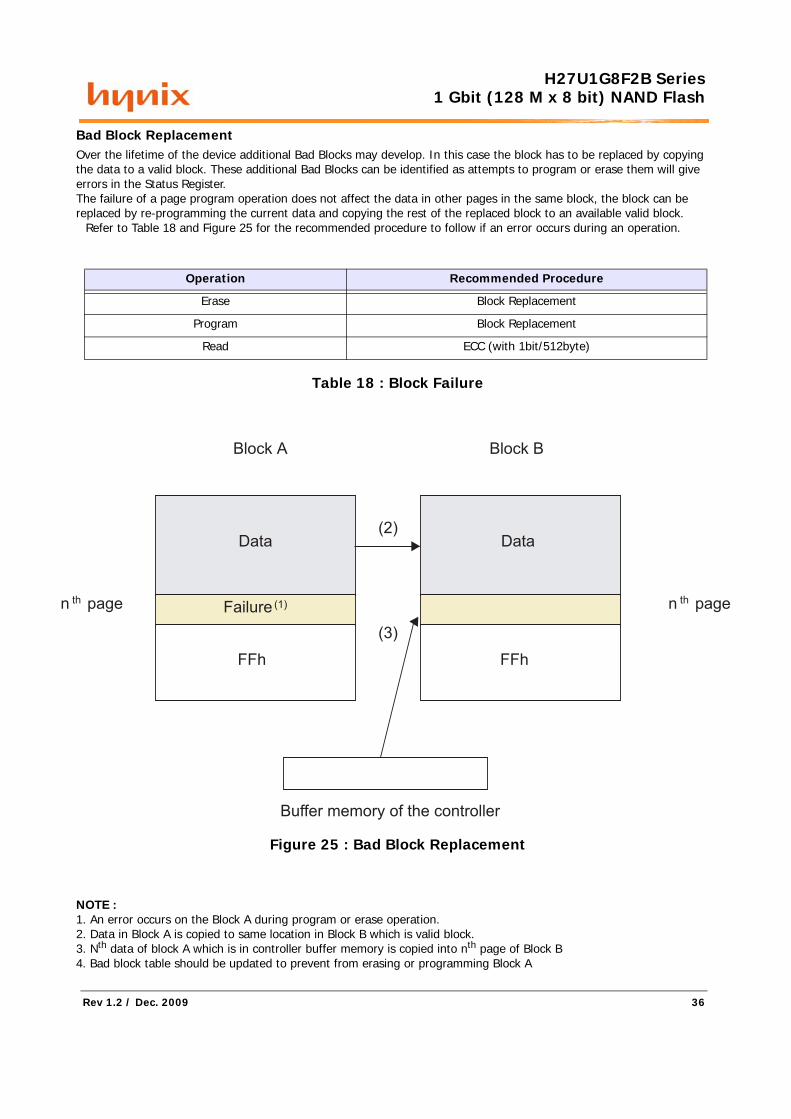
Bad Block ReplacementOver the lifetime of the device additional Bad Blocks may develop. In this case the block has to be replaced by copying the data to a valid block. These additional Bad Blocks can be identified as attempts to program or erase them will give errors in the Status Register.The failure of a page program operation does not affect the data in other pages in the same block, the block can be replaced by re-programming the current data and copying the rest of the replaced block to an available valid block.
Refer to Table 18 and Figure 25 for the recommended procedure to follow if an error occurs during an operation.
Table 18 : Block Failure
Figure 25 : Bad Block Replacement
NOTE : 1. An error occurs on the Block A during program or erase operation.2. Data in Block A is copied to same location in Block B which is valid block.3. Nth data of block A which is in controller buffer memory is copied into nth page of Block B4. Bad block table should be updated to prevent from erasing or programming Block A
Operation Recommended Procedure
Erase Block Replacement
Program Block Replacement
Read ECC (with 1bit/512byte)

Rev 1.2 / Dec. 2009 37
1
H27U1G8F2B Series1 Gbit (128 M x 8 bit) NAND Flash
80h 10h
tWW
WE
I/Ox
WP
R/B
WWt
80h 10h
WE
I/Ox
WP
R/B
60h
tWW
D0h
WE
I/Ox
WP
R/B
60h
t
D0h
WW
WE
I/Ox
WP
R/B
Write Protect Operation
The Erase and Program Operations are automatically reset when WP goes Low (tWW = 100ns, min). The operations areenabled and disabled as follows (Figure 26~29)
Figure 26 : Enable Programming Figure 27 : Disable Programming
Figure 28 : Enable Erasing Figure 29 : Disable Erasing

Rev 1.2 / Dec. 2009 38
1
H27U1G8F2B Series1 Gbit (128 M x 8 bit) NAND Flash
Figure 30. 48-TSOP1 - 12 x 20mm, Package Outline
Table 19. 48-TSOP1 - 12 x 20mm, Package Mechanical Data
Symbolmillimeters
Min Typ Max
A 1.200
A1 0.050 0.150
A2 0.980 1.030
B 0.170 0.250
C 0.100 0.200
CP 0.100
D 11.910 12.000 12.120
E 19.900 20.000 20.100
E1 18.300 18.400 18.500
e 0.500
L 0.500 0.680
alpha 0 5

Rev 1.2 / Dec. 2009 39
1
H27U1G8F2B Series1 Gbit (128 M x 8 bit) NAND Flash
Figure 31. 63-ball FBGA - 9 x 11 ball array 0.8mm pitch, Package Outline
Table 20. 63-ball FBGA - 9 x 11 ball array 0.8mm pitch, Package Mechanical Data
Symbolmillimeters
Min Typ Max
A 0.80 0.90 1.00
A1 0.25 0.30 0.35
A2 0.55 0.60 0.65
b 0.40 0.45 0.50
D 8.90 9.00 9.10
D1 4.00
D2 7.20
E 10.90 11.00 11.10
E1 5.60
E2 8.80
e 0.80
FD 2.50
FD1 0.90
FE 2.70
FE1 1.10
SD 0.40
SE 0.40

Rev 1.2 / Dec. 2009 40
1
H27U1G8F2B Series1 Gbit (128 M x 8 bit) NAND Flash
MARKING INFORMATION - TSOP1 / FBGA
M arking Exam ple
K O R
H 2 7 U 1 G 8 F 2 B
Y W W x x
- hynix
- KO R
- H 27U1G8F2Bxx-xx
H : Hynix
27: NAND Flash
U : Power Supply
1G: Density
8 : Bit O rganization
F: Classification
2 : Mode
B : Version
x: Package Type
x: Package Material
x: Bad B lock
x: Operating Tem perature
- Y: Year (ex: 8=year 2008, 9= year 2009)
- w w : W ork W eek (ex: 12= work week 12)
- xx: Process Code
N ote
- Capital Letter
- Sm all Letter
: Hynix Sym bol
: Origin Country
: U (2.7 V~3.6 V)
: 1 Gbit
: 8(x8)
: Single Level Cell+Single D ie+Large Block
: 2(1nCE & 1R/nB; Sequentia l Row Read D isable)
: 3rd Generation
: T(48-TSOP1), F(63-FBGA)
: B lank(Norm al), R(Lead & Halogen Free)
: B(Included Bad B lock), S(1~5 Bad Block),
P(All Good Block)
: C(0℃~70℃ ), I(-40℃~85℃ )
: Fixed Item
: Non-fixed Item
: Part Num ber
x x - x x