i. academic/professional background
TRANSCRIPT
PPS 8.10 Form 1A
Page 1 of 36
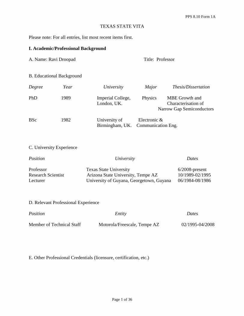
TEXAS STATE VITA
Please note: For all entries, list most recent items first.
I. Academic/Professional Background
A. Name: Ravi Droopad Title: Professor
B. Educational Background
Degree Year University Major Thesis/Dissertation
PhD 1989 Imperial College, Physics MBE Growth and
London, UK. Characterisation of
Narrow Gap Semiconductors
BSc 1982 University of Electronic &
Birmingham, UK. Communication Eng.
C. University Experience
Position University Dates
Professor Texas State University 6/2008-present
Research Scientist Arizona State University, Tempe AZ 10/1989-02/1995
Lecturer University of Guyana, Georgetown, Guyana 06/1984-08/1986
D. Relevant Professional Experience
Position Entity Dates
Member of Technical Staff Motorola/Freescale, Tempe AZ 02/1995-04/2008
E. Other Professional Credentials (licensure, certification, etc.)

PPS 8.10 Form 1A
Page 2 of 36
II. TEACHING
A. Teaching Honors and Awards:
B. Courses Taught:
PHYS 2435
PHYS 5326
EE 4353
MFGE 4392
ENGR 5100
EE 5360
C. Graduate Theses/Dissertations or Exit Committees (if supervisor, please indicate):
Thesis Committee: Jennifer Walters, MSc – Decembert 2009
Thesis Committee: Daniel Moody, MSc – August 2011
Thesis Committee: Dominic Chiroro, MSc – April 2012
Chair, Thesis Committee: Thiess Cunningham, MSc – November 2012
Thesis Committee: Rye Johnson, MSc – April 2013
Thesis Committee: Chad Waxler, MSc- April 2013
Thesis Committee: Nelson Simpson , MSc- May 2013
Chair: Thesis Committee: Rico Garza, MSc-December 2013
Chair: Thesis Committee: Hanu Arava MSc- June 2014
PhD Thesis Committee: Ray Cook- June 2014
PhD Thesis Committee: Paul Thomas, RIT – June 2015
Chair, PhD Thesis Committee: Kunal Bhatnagar- June 2015
Chair, PhD Thesis Committee: Javad Rezanezhad –April 2016
Chair, PhD Thesis Committee: Md Shafiqur Rahman – April 2017
Thesis Committee: Fidele Twagirayezu MSc – May 2017
Chair, PhD Thesis Committee: Susmita Ghose – July 2017
Thesis Committee: Mahmuda Akter Monne MSc – June 2017
Thesis Committee: Evarestus Enuka MSc – June 2017
Thesis Committee: Md Abdul Ahad Talukder MSc – June 2017
Thesis Committee: John Peterson, PhD – October 2017
Thesis Committee: Shelby Huff MSc – November 2017
Thesis Committee: Ooha Manda MSc – November 2017
Thesis Committee: Mohi Uddin Jewel MSc – June 2018
Thesis Committee: Liang Hong (U. Illinois, Chicago) PhD – July 2018
Chair, Thesis Committee: Brian Samuels MSc– August 2018
Thesis Committee: Tarun Kadukuntla MSc – October 2019
D. Courses Prepared and Curriculum Development:
EE 5360: Thin Film Technology
E. Funded External Teaching Grants and Contracts:

PPS 8.10 Form 1A
Page 3 of 36
F. Submitted, but not Funded, External Teaching Grants and Contracts:
G. Funded Internal Teaching Grants and Contracts:
H. Submitted, but not Funded, Internal Teaching Grants and Contracts:
I. Other:
III. SCHOLARLY/CREATIVE
A. Works in Print
1. Books (if not refereed, please indicate)
a. Scholarly Monographs:
b. Textbooks:
c. Edited Books:
Crystalline Oxide-Silicon Heterostructures and Oxide Optoelectronics, edited by D.
Ginley, S. Guha, S. Carter, S.A. Chambers, R. Droopad, H. Hosono, D.C. Paine, D.G.
Schlom, and J. Tate, Vol. 747 (Materials Research Society, Warrendale, 2003).
d. Chapters in Books:
High-K Crystalline Gate Dielectrics – An IC Manufacturer’s Perspective – R. Droopad,
K. Eisenbeiser, A.A. Demkov “High Dielectric Constant Materials- VLSI MOSFET
Applications” – Springer Series in Advanced Microelectronic, 2004
Gallium Oxide on Gallium Arsenide: Atomic Structure, Materials and Devices – M.
Passlack, Z. Yu, R. Droopad, J. Abrokwah, D. Braddock, S. Yi, M. Hale, J. Sexton, A.
Kummel “III-V Semiconductor Heterostructures: Physics and Devices” – Research
PPS 8.10 Form 1A
Page 4 of 36
Signpost, 2003
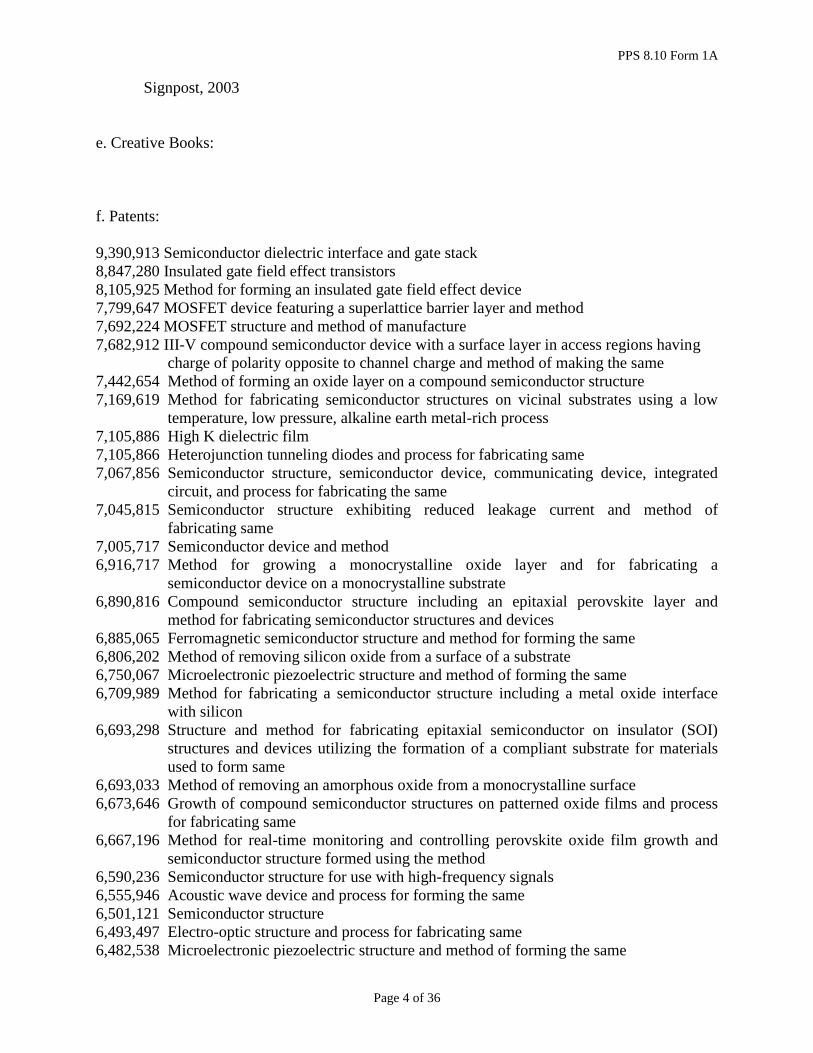
e. Creative Books:
f. Patents:
9,390,913 Semiconductor dielectric interface and gate stack
8,847,280 Insulated gate field effect transistors
8,105,925 Method for forming an insulated gate field effect device
7,799,647 MOSFET device featuring a superlattice barrier layer and method
7,692,224 MOSFET structure and method of manufacture
7,682,912 III-V compound semiconductor device with a surface layer in access regions having
charge of polarity opposite to channel charge and method of making the same
7,442,654 Method of forming an oxide layer on a compound semiconductor structure
7,169,619 Method for fabricating semiconductor structures on vicinal substrates using a low
temperature, low pressure, alkaline earth metal-rich process
7,105,886 High K dielectric film
7,105,866 Heterojunction tunneling diodes and process for fabricating same
7,067,856 Semiconductor structure, semiconductor device, communicating device, integrated
circuit, and process for fabricating the same
7,045,815 Semiconductor structure exhibiting reduced leakage current and method of
fabricating same
7,005,717 Semiconductor device and method
6,916,717 Method for growing a monocrystalline oxide layer and for fabricating a
semiconductor device on a monocrystalline substrate
6,890,816 Compound semiconductor structure including an epitaxial perovskite layer and
method for fabricating semiconductor structures and devices
6,885,065 Ferromagnetic semiconductor structure and method for forming the same
6,806,202 Method of removing silicon oxide from a surface of a substrate
6,750,067 Microelectronic piezoelectric structure and method of forming the same
6,709,989 Method for fabricating a semiconductor structure including a metal oxide interface
with silicon
6,693,298 Structure and method for fabricating epitaxial semiconductor on insulator (SOI)
structures and devices utilizing the formation of a compliant substrate for materials
used to form same
6,693,033 Method of removing an amorphous oxide from a monocrystalline surface
6,673,646 Growth of compound semiconductor structures on patterned oxide films and process
for fabricating same
6,667,196 Method for real-time monitoring and controlling perovskite oxide film growth and
semiconductor structure formed using the method
6,590,236 Semiconductor structure for use with high-frequency signals
6,555,946 Acoustic wave device and process for forming the same
6,501,121 Semiconductor structure
6,493,497 Electro-optic structure and process for fabricating same
6,482,538 Microelectronic piezoelectric structure and method of forming the same

PPS 8.10 Form 1A
Page 5 of 36
6,479,173 Semiconductor structure having a crystalline alkaline earth metal silicon nitride/oxide
interface with silicon
6,472,276 Using silicate layers for composite semiconductor
6,432,546 Microelectronic piezoelectric structure and method of forming the same
6,392,257 Semiconductor structure, semiconductor device, communicating device, integrated
circuit, and process for fabricating the same
2. Articles
a. Refereed Journal Articles:
221. Scaling and mechanism of droplet array formation on a laser-ablated
superhydrophobic grid, Bahador Farshchian, Javad R. Gatabi, Steven M. Bernick,
Gwan-Hyoung Lee, Ravindranath Droopad, Namwon Kim, Colloids and Surfaces A,
547 (2018) 49-55.
220. Bias temperature stress induced hydrogen depassivation from Al2O3/InGaAs interface defects,
Kechao Tang, Ravi Droopad, Paul C. McIntyre, J. Appl. Physics 123 (2018) 025708
219 Structural, Optical, and Electrical Characterization of beta-Ga2O3 Thin Films Grown by
Plasma-Assisted Molecular Beam Epitaxy Suitable for UV Sensing, A. N. Nedev, S. Ghose, J.
S. Rojas-Ramirez, D. Mateos, M. C. Alverez, O. Perez, M. Saurez, B. Valdez-Salas, R.
Droopad, Adv. Mat. Sci & Eng (2018) 9450157
218. Efficiency of broadband terahertz rectennas based on self-switching nanodiodes, E.
Briones, I. E. Cortes-Mestizo, J. Briones , R. Droopad, L. I. Espinosa-Vega, H.
Vilchis, V. H. Mendez-Garcia, J. Photonics for Energy, 7 (2017) 25001
217. Optical spectroscopy analysis of the near surface depletion layer in AlGaAs/GaAs
heterostructures grown by MBE, I. E. Cortes-Mestizo, E. Briones, C. M. Yee-Rendon,
L. Zamora Peredo, L. I. Espinosa-Vega, R. Droopad, V. H. Mendez-Garcia, J. Cryst.
Growth, 477 (2017) 59-64
216. Growth and characterization of Ga2O3 thin films by molecular beam epitaxy for deep-
UV photodetectors, Susmita Ghose, Shafiqur Rahman, Liang Hong, Juan Salvador
Rojas-Ramirez, Hanbyul Jin, Kibog Park, Robert Klie, and Ravi Droopad, J. Appl.
Phys. 122, (2017) 095302
215. Atomic-scale structural and electronic properties of SrTiO3/GaAs interfaces: A
combined STEM-EELS and first-principles study, Liang Hong, Kunal Bhatnagar, Ravi
Droopad, Robert F. Klie, and Serdar Ö̆güt, Phys. Rev. B 96 (2017) 035311
214. Tuning electrical properties of PZT film deposited by Pulsed Laser Deposition,
J.R.Gatabi, S. Rahman, A. Amaro, T. Nash, J. Rojas-Ramirez, R. K. Pandey, R.
Droopad, Ceramics Intl. 43 (2017) 6008

PPS 8.10 Form 1A
Page 6 of 36
213. Self-limiting CVD of a passivating SiOx control layer on InGaAs(001)-(2x4) with the
prevention of III-V oxidation, M. Edmonds, S. Wolf, E. Chagarov, T. Kent, J.H. Park,
R. Holmes, D. Alvarez, R. Droopad, A.C.Kummel, Surf. Sci. 660 (2017) 31
212. Interface Defect Hydrogen Depassivation and Capacitance-Voltage Hysteresis of
Al2O3/InGaAs Gate Stacks, K.C.Tang, F.R. Palumbo, L.L.Zhang, R. Droopad, P.C.
McIntyre, ACS Appl. Mat. & Interfaces 9 (2017) 7819
211. A crystalline oxide passivation on In0.53Ga0.47As (100), Xiaoye Qin, Wei-E Wang,
Ravi Droopad, Mark S. Rodder, and Robert M. Wallace, J. of Appl. Phys. 121, 125302
(2017)
210. Temperature Dependent Border Trap Response Produced by a Defective Interfacial
Oxide Layer in Al2O3/InGaAs Gate Stacks, Kechao Tang, Andrew C. Meng, Ravi
Droopad, and Paul C. McIntyre, ACS Appl. Mater. Interfaces 2016, 8, 30601
209. Laser-induced superhydrophobic grid patterns on PDMS for droplet arrays formation,
Bahador Farshchian, Javad R. Gatabi, Steven M. Bernicka, Sooyeon Park, Gwan-
Hyoung Lee, Ravindranath Droopad, Namwon Kim, Applied Surface Science 396
(2017) 359
208. The impact of forming gas annealing on the electrical characteristics of sulfur
passivated Al2O3/In0.53Ga0.47As (110) metal-oxide-semiconductor capacitors, Yen-
Chun Fu, Uthayasankaran Peralagu, David A. J. Millar, Jun Lin, Ian Povey, Xu Li,
Scott Monaghan, Ravi Droopad, Paul K. Hurley, and Iain G. Thayne, Appl. Phys. Lett.
110, 142905 (2017);
207. InAs Nanowire GAA n-MOSFETs with 12-15 nm Diameter, T. Vasen, P. Ramvall, A.
Afzalian, C. Thelander, K. A. Dick, M. Holland, G. Doornbos, S. W. Wang, R.
Oxland, G. Velliantis, M. J. H. van Dal, B. Duriez, J. Rojas-Ramirez, R. Droopad, L.
E. Wernersson, L. Samuelson, T. K. Chen, Y. -C. Yeo, M. Passlack, 2016 IEEE
SYMPOSIUM ON VLSI TECHNOLOGY
206. In0.53Ga0.47As(001)-(2x4) and Si0.5Ge0.5(110)surface passivation by self-limiting
deposition of silicon containing control layers, M. Edmonds, T. J. Kent, S. Wolf, K.
Sardashti, M. Chang, J. Kachian, R. Droopad, E. Chagarov, and A. C. Kummel, 2016
INTERNATIONAL SYMPOSIUM ON VLSI TECHNOLOGY, SYSTEMS AND
APPLICATION (VLSI-TSA)
205. A Nonlinear Circuit Simulation of Switching Process in Resonant Tunneling Diodes,
W.-D. Zhang, E. R. Brown, T. A. Growden, P. R. Berger, R. Droopad, IEEE Trans. on
Elect. Device, 63 (2016)4993
204. Integration of BiFeO3/La0.7Sr0.3MnO3 heterostructures with III-V semiconductors
for low-power non-volatile memory and multiferroic field effect transistors, Rahman,
Md Shafiqur, Ghose, Susmita, Hong, Liang, Dhungana, Pradip, Fahami, Abbas,
Gatabi, Javad R., Rojas-Ramirez, Juan S., Zakhidov, Alex, Klie, Robert F., Pandey, R.
K., Droopad, Ravi, J. Mat. Chem. 4 (2016) 10386

PPS 8.10 Form 1A
Page 7 of 36
203. Temperature Dependent Border Trap Response Produced by a Defective Interfacial
Oxide Layer in Al2O3/InGaAs Gate Stacks, Tang, Kechao, Meng, Andrew C.,
Droopad, Ravi, McIntyre, Paul C., ACS Appl. Mat. & Interface 8 (2016) 30601
202. Performance evaluation of broken gap Esaki tunnel diodes on Si and GaSb substrates,
P. M. Thomas, M. J. Filmer ; A. Gaur ; S. L. Rommel ; K. Bhatnagar (DST) ; R.
Droopad, Electronic Letts. 52 (2016) 73
201. InAs FinFETs With H-fin=20 nm Fabricated Using a Top-Down Etch Process, R.
Oxland , X. Li ; S. W. Chang ; S. W. Wang ; T. Vasen ; P. Ramvall ; R. Contreras-
Guerrero ; J. Rojas-Ramirez ; M. Holland ; G. Doornbos ; Y. S. Chang ; D. S.
Macintyre ; S. Thoms ; R. Droopad ; Y. -C. Yeo ; C. H. Diaz ; I. G. Thayne ; M.
Passlack, IEEE Elect. Dev. Letts. 37 (2016) 261
200. Determination of the depletion layer width and effects on the formation of double-
2DEG in AlGaAs/GaAs heterostructures, Irving Eduardo Cortes-Mestizo, Leticia
Ithsmel Espinosa-Vega, Jose Angel Espinoza-Figueroa, Alejandro Cisneros-de-la-Rosa,
Eric Eugenio-Lopez, Victor Hugo Mendez-Garcia, Edgar Briones, Joel Briones, Luis
Zamora-Peredo, Ravindranath Droopad and Cristo Yee-Rendon, J. Vac. Sci. Tech. B34
(2016) 02L110-1
199. Structural and optical properties of beta-Ga2O3 thin films grown by plasma-assisted
molecular beam epitaxy, S. Ghose, M.S. Rahman, J. S. Rojas-Ramirez, M. Caro, R.
Droopad, A. Arias, N. Nedev, J. Vac. Sci. Tech. B34 (2016) 02L109-1
198. Study of InAlAs/InGaAs self-switching diodes for energy harvesting applications, Irving
Eduardo Cortes-Mestizo, Edgar Briones, Joel Briones, Ravindranath Droopad, Manuel
Perez-Caro, Stefan McMurtry, Michel Hehn, François Montaigne, and Victor Hugo
Mendez-Garcia, Japanese Journal of Applied Physics 55, 014304 (2016)
197. Terahertz harvesting with shape-optimized InAlAs/InGaAs self-switching nanodiodes,
Irving Cortes-Mestizo, Victor H. Méndez-García, Joel Briones, Manuel Perez-Caro,
Ravi Droopad, Stefan McMurtry, Michel Hehn, François Montaigne, and Edgar Briones,
AIP Advances 5, 117238 (2015)
196. The influence of surface preparation on low temperature HfO2 ALD on InGaAs (001)
and (110) surfaces, Tyler Kent, Kechao Tang, Varistha Chobpattana, Muhammad Adi
Negara, Mary Edmonds, William Mitchell, Bhagawan Sahu, Rohit Galatage, Ravi
Droopad, Paul McIntyre, and Andrew C. Kummel, J. of Chem. Phys. 143, 164711
(2015).
195. Integration of broken-gap heterojunction InAs/GaSb Esaki tunnel diodes on silicon,
Kunal Bhatnagar, Manuel P. Caro, Juan S. Rojas-Ramirez, Ravi Droopad, Paul M.
Thomas, Abhinav Gaur, Matthew J. Filmer, and Sean L. Rommel, J.Vac. Sci. &
Technol. B 33, 062203 (2015)
194 Direct observation of oxygen-vacancy-enhanced polarization in a SrTiO3-buffered
ferroelectric BaTiO3 film on GaAs, Qiao Qiao, Yuyang Zhang, Rocio Contreras-

PPS 8.10 Form 1A
Page 8 of 36
Guerrero, Ravi Droopad, Sokrates T. Pantelides, Stephen J. Pennycook, Serdar Ogut,
and Robert F. Klie, Appl. Phys. Letts. 107, 201604 (2015)
193. Border trap reduction in Al2O3/InGaAs gate stacks, Kechao Tang, Roy Winter,
Liangliang Zhang, Ravi Droopad, Moshe Eizenberg, and Paul C. McIntyre, Appl. Phys.
Letts. 107, 202102 (2015)
192. Experimental determination of quantum-well lifetime effect on large-signal resonant
tunneling diode switching time, Tyler A. Growden, E. R. Brown, Weidong Zhang, Ravi
Droopad, and Paul R. Berger, Appl. Phys. Letts. 107, 153506 (2015)
191. Field-Effect Mobility of InAs Surface Channel nMOSFET With Low D-it Scaled Gate-
Stack, S.W. Wang, T. Vasen, G. Doornbos, R. Oxland, S. W. Chang, X. Li, R.
Contreras-Guerrero, M. Holland, C. H. Wang, M. Edirisooriya, J. S. Rojas-Ramirez, P.
Ramvall, S. Thoms, D.S. Macintyre, G. Vellianitis, G.C.H. Hsieh, Y.S. Chang, K.M.
Yin, Y.C. Yeo, C.H. Diaz, R. Droopad, I.G. Thayne, M. Passlack, IEEE Trans.
Electron. Devices, 62 (1015) 2429
190. Performance Evaluation of In0.53Ga0.47As Esaki Tunnel Diodes on Silicon and InP
Substrates, P. Thomas, M. Filmer, A. Gaur, D.J. Pawlik, B. Romanczyk, E. Marini, S.L.
Rommel, K. Majumdar, W.Y. Loh, M.H. Wong, C. Hobbs, K. Bhatnagar, R. Contreras-
Guerrero, R. Droopad, IEEE Trans. Electron. Devices, 62 (2015) 2450
189. Passivation of InGaAs(001)-(2 x 4) by Self-Limiting Chemical Vapor Deposition of a
Silicon Hydride Control Layer, M. Edmonds, T. Kent, E. Chagarov, K. Sardashti, R.
Droopad, M. Chang, J. Kachian, J.H. Park, A. Kummel, J. Am. Chem. Soc. 137 (2015)
8526
188. Dual Passivation of Intrinsic Defects at the Compound Semiconductor/Oxide Interface
Using an Oxidant and a Reductant, T. Kent, E. Chagarov, M. Edmonds, R. Droopad,
A.C. Kummel, ACS Nano 9 (2015) 4843-4849
187. Fabrication and characterization of sub-micron In0.53Ga0.47As p-i-n diodes, A. Gaur,
M. Filmer, P. Thomas, K. Bhatnagar, R. Droopad, S. Rommel, Solid State Electronics,
111 (2015) 234-237
186. Functional materials integrated on III–V semiconductors, Javad Gatabi, Kevin Lyon,
Shafiqur Rahman, Manuel Caro, Juan Rojas-Ramirez, Joelson Cott-Garcia, Ravi
Droopad, Byounghak Lee, Microelectronic Engineering 147 (2015) 117–121
185. Electrical and Optical Properties of LiNbO3/CaCu3Ti4O12 heterostructures on Si, Javad
R. Gatabi, Kevin A. Lyon, Shafiqur Rahman, Hanu Arava, Juan S Rojas-Ramirez, R. K.
Pandey, Ravi Droopad, to be published in MRS proceedings, 2015
184. In-situ monitoring during MBE growth of InAs based heterostructures, Kunal
Bhatnagar, Juan Rojas-Ramirez, Manuel Caro, Rocio Contreras, Bernd Henninger,
Ravi Droopad, Journal of Crystal Growth. Volume 425, (2015) 16–20
PPS 8.10 Form 1A
Page 9 of 36
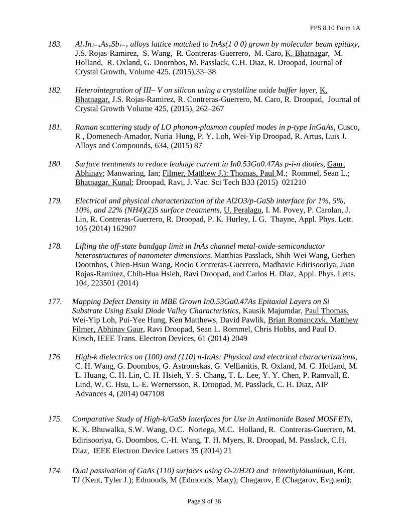
183. AlxIn1−xAsySb1−y alloys lattice matched to InAs(1 0 0) grown by molecular beam epitaxy,
J.S. Rojas-Ramirez, S. Wang, R. Contreras-Guerrero, M. Caro, K. Bhatnagar, M.
Holland, R. Oxland, G. Doornbos, M. Passlack, C.H. Diaz, R. Droopad, Journal of
Crystal Growth, Volume 425, (2015),33–38
182. Heterointegration of III– V on silicon using a crystalline oxide buffer layer, K.
Bhatnagar, J.S. Rojas-Ramirez, R. Contreras-Guerrero, M. Caro, R. Droopad, Journal of
Crystal Growth Volume 425, (2015), 262–267
181. Raman scattering study of LO phonon-plasmon coupled modes in p-type InGaAs, Cusco,
R , Domenech-Amador, Nuria Hung, P. Y. Loh, Wei-Yip Droopad, R. Artus, Luis J.
Alloys and Compounds, 634, (2015) 87
180. Surface treatments to reduce leakage current in In0.53Ga0.47As p-i-n diodes, Gaur,
Abhinav; Manwaring, Ian; Filmer, Matthew J.); Thomas, Paul M.; Rommel, Sean L.;
Bhatnagar, Kunal; Droopad, Ravi, J. Vac. Sci Tech B33 (2015) 021210
179. Electrical and physical characterization of the Al2O3/p-GaSb interface for 1%, 5%,
10%, and 22% (NH4)(2)S surface treatments, U. Peralagu, I. M. Povey, P. Carolan, J.
Lin, R. Contreras-Guerrero, R. Droopad, P. K. Hurley, I. G. Thayne, Appl. Phys. Lett.
105 (2014) 162907
178. Lifting the off-state bandgap limit in InAs channel metal-oxide-semiconductor
heterostructures of nanometer dimensions, Matthias Passlack, Shih-Wei Wang, Gerben
Doornbos, Chien-Hsun Wang, Rocio Contreras-Guerrero, Madhavie Edirisooriya, Juan
Rojas-Ramirez, Chih-Hua Hsieh, Ravi Droopad, and Carlos H. Diaz, Appl. Phys. Letts.
104, 223501 (2014)
177. Mapping Defect Density in MBE Grown In0.53Ga0.47As Epitaxial Layers on Si
Substrate Using Esaki Diode Valley Characteristics, Kausik Majumdar, Paul Thomas,
Wei-Yip Loh, Pui-Yee Hung, Ken Matthews, David Pawlik, Brian Romanczyk, Matthew
Filmer, Abhinav Gaur, Ravi Droopad, Sean L. Rommel, Chris Hobbs, and Paul D.
Kirsch, IEEE Trans. Electron Devices, 61 (2014) 2049
176. High-k dielectrics on (100) and (110) n-InAs: Physical and electrical characterizations,
C. H. Wang, G. Doornbos, G. Astromskas, G. Vellianitis, R. Oxland, M. C. Holland, M.
L. Huang, C. H. Lin, C. H. Hsieh, Y. S. Chang, T. L. Lee, Y. Y. Chen, P. Ramvall, E.
Lind, W. C. Hsu, L.-E. Wernersson, R. Droopad, M. Passlack, C. H. Diaz, AIP
Advances 4, (2014) 047108
175. Comparative Study of High-k/GaSb Interfaces for Use in Antimonide Based MOSFETs,
K. K. Bhuwalka, S.W. Wang, O.C. Noriega, M.C. Holland, R. Contreras-Guerrero, M.
Edirisooriya, G. Doornbos, C.-H. Wang, T. H. Myers, R. Droopad, M. Passlack, C.H.
Diaz, IEEE Electron Device Letters 35 (2014) 21
174. Dual passivation of GaAs (110) surfaces using O-2/H2O and trimethylaluminum, Kent,
TJ (Kent, Tyler J.); Edmonds, M (Edmonds, Mary); Chagarov, E (Chagarov, Evgueni);

PPS 8.10 Form 1A
Page 10 of 36
Droopad, R (Droopad, Ravi ; Kummel, AC (Kummel, Andrew C.), J. of Chemical
Physics, Vol. 139 (2013) 244706
173. InAs hole inversion and bandgap interface state density of 2x1011 cm-2eV-1 at HfO2/InAs
interfaces, C. H. Wang,1, S. W. Wang, G. Doornbos, G. Astromskas, K. Bhuwalka, R.
Contreras-Guerrero, M. Edirisooriya, J. S. Rojas-Ramirez, G. Vellianitis, R. Oxland, M.
C. Holland, C. H. Hsieh, P. Ramvall, E. Lind, W. C. Hsu, L.-E. Wernersson, R. Droopad,
M. Passlack, and C. H. Diaz, Appl. Phys Letts 103, (2013) 143510
172. Properties of epitaxial BaTiO3 deposited on GaAs, R. Contreras-Guerrero, J. P. Veazey,
J. Levy, R. Droopad, Appl Phys Letts. 102 (2013) 012907
171. Interface properties of MBE grown epitaxial oxides on GaAs, R. Contreras-Guerrero, M.
Edirisooriya, O.C. Noriega, R. Droopad, Journal of Crystal Growth, Journal of Crystal
Growth 378 (2013) 238–242
170. Growth of heterostructures on InAs for high mobility device applications, R. Contreras-
Guerrero, S. Wang, M. Edirisooriya, W. Priyantha, J.S. Rojas-Ramirez, K. Bhuwalka, G.
Doornbos, M. Holland, R. Oxland, G. Vellianitis, M. Van Dal, B. Duriez, M. Passlack,
C.H. Diaz, R. Droopad Journal of Crystal Growth, , Journal of Crystal Growth 378 (2013)
117–120
169. Characterization of anti-phase boundaries in hetero-epitaxial polar-on-nonpolar
semiconductor films by optical second-harmonic generation, Ming Lei, J. Price, Wei-E
Wang, Man Hoi Wong, Ravi Droopad, Paul Kirsch, G. Bersuker, and M. C. Downer,
Appl Phys Letts. 102 (2013) 152103
168. Magnetic and structural properties of BiFeO3 thin films grown epitaxially on SrTiO3/Si
substrates, Ryan P. Laughlin, Daniel A. Currie, Rocio Contreras-Guererro, Aruna
Dedigama, Weerasinghe Priyantha, Ravindranath Droopad, Nikoleta Theodoropoulou,
Peng Gao, Xiaoqing Pan, J. Appl. Phys. 113, 17D919 (2013)
167. Epitaxial ferroelectric oxides on semiconductors- A route towards negative capacitance
devices, R. Droopad, R. Contreras-Guerrero, J.P. Veazey, Q. Qiao, R.F. Klie, J. Levy,
Microelectronic Engineering, 109, (2013) 290-293
166. MOVPE-grownInAs/AlAs0.16Sb0.84/InAs and InAs/AlAs0.16Sb0.84/GaSb
heterostructures, P.Ramvall, C.H.Wang, G.Astromskas, G.Vellianitis, M.Holland,
R.Droopad, L. Samuelson, L.E.Wernersson, M.Passlack, C.H.Diaz, ,Journal of Crystal
Growth 374 (2013) 43–48
165. An ultra-low resistance, ultra-shallow, metallic source-drain contact scheme for III-V
NMOS, R. Oxland, S.W. Chang, Xu Li, S.W. Wang, G. Radhakrishnan, W. Priyantha,
M.J.H. van Dal, C.H. Hsieh, G. Vellianitis, G. Doornbos, K. Bhuwalka, B. Duriez, I.
Thayne, R. Droopad, M. Passlack, C.H. Diaz, Y.C. Sun, IEEE Electron Device
Letts Volume: 33 Issue: 4 Pages: 501-503

PPS 8.10 Form 1A
Page 11 of 36
164. Structure of V thin films on Al(100) using XPD, LEED, and LEIS, Priyantha, W.
Droopad, R.; Kopczyk, M.; Smith, R.J.; Kayani, A., Surface Science 606 (2012) 1160–
1166
163. Scanning probe microscopy imaging before and after atomic layer oxide deposition on a
compound semiconductor surface , W. Melitz, J.B. Clemens, J. Shen, E.A. Chagarov, S.
Lee, J.S. Lee, J.E. Royer, M. Holland, S. Bentley, D. McIntyre, I. Thayne, R. Droopad,
A.C. Kummel , Solid State Phenomena, 187 , pgs 9-10 ( 2012)
162. Challenges of III-V materials in advanced CMOS logic, Kirsch, P.D. Hill, R.J.W.;
Huang, J.;Loh, W.Y.; Kim, T.-W.; Wong, M.H.; Min, B.G.; Huffman, C.; Veksler,
D.; Young, C.D.;Ang, K.W.; Ali, I.; Lee, R.T.P.; Ngai, T.; Wang, A.; Wang, W.-
E.; Cunningham, T.H.;Chen, Y.T.; Hung, P.Y.; Bersch, E.; Sassman, B.; Cruz,
M.; Trammell, S.; Droopad, R.; Oktybrysky, S.; Lee, J.C.; Bersuker, G.; Hobbs,
C.; Jammy, R., Proceedings of the 2012 International Symposium on VLSI Technology,
Systems and Application (VLSI-TSA), p 2 pp., 2012
161. Atomic imaging of atomic layer deposition oxide nucleation with trimethylaluminum on
As-rich InGaAs(001) 2 × 4 vs In-rich InGaAs(001) 4 × 2, Melitz, Wilhelm; Kent, Tyler;
Kummel, Andrew C.; Droopad, Ravi; Holland, Martin; Thayne, Iain; Journal of
Chemical Physics, Vol. 136, no. 15, ( 2012)
160. Integration challenges of III-V materials in advanced CMOS logic, Hill, R.J.W.; Huang,
J.; Loh, W.Y.; Kim, T.; Wong, M.H.; Veksler, D.; Cunningham, T.H.; Droopad, R.; Oh,
J.; Hobbs, C.; Kirsch, P.D.; Jammy, R., ECS Transactions, v 45, n 6, p 179-184, 2012,
Silicon Compatible Materials, Processes, and Technologies for Advanced Integrated
Circuits and Emerging Applications 2
159. InGaAs surface preparation for atomic layer deposition by hydrogen cleaning and
improvement with high temperature anneal , Melitz Wilhelm; Shen Jian; Kent Tyler;
Andrew C. Kummel, Ravi Droopad, Journal of Applied Physics, v 110, n 1, July 1, 2011
158. In-situ XPS and RHEED study of gallium oxide on GaAs deposition by molecular beam
epitaxy, W. Priyantha, G. Radhakrishnan, R. Droopad, M. Passlack, M. Journal of
Crystal Growth, v 323, n 1, p 103-106, May 15, 2011
157. Scanning tunneling microscopy study of the interfacial bonding structures of Ga(2)O
and In(2)O/In(0.53)Ga(0.47)As(001) , Jian Shen, Darby Feldwinn, Wilhelm Melitz, Ravi
Droopad, Andrew C. Kummel, Microelectronic Engineering, v 88, n 4, p 377-382, April
2011
156. Atomic imaging of atomic H cleaning of InGaAs and InP for ALD, Wilhelm Melitz, Jian
Shen, Tyler Kent, Ravi Droopad, Paul Hurley, Andrew C. Kummel, ECS Transactions, v
35, n 4, p 175-189, 2011, Silicon Nitride, Silicon Dioxide, and Emerging Dielectrics 11
155. Atomic-layer-deposited LaAlO3/SrTiO3 all oxide field-effect transistors, L. Dong, Y.Q
Liu, M. Xu, Y.Q Wu, R. Colby, E.A Stach, R. Droopad, R. G.Gordon, P.D Ye, 2010

PPS 8.10 Form 1A
Page 12 of 36
IEDM - TECHNICAL DIGEST Book Series: International Electron Devices
Meeting Published: 2010
154. Interfacial atomic bonding structure of oxides on InAs (001) - (4x2) surface, Shen Jian,
Melitz, Wilhelm, Lee, Sangyeob, Feldwinn, Darby L., Droopad, Ravi, Kummel, Andrew
C., Journal of the Electrochemical Society, v157, (2010) p H1148-H1152
153. Atomic imaging of the monolayer nucleation and unpinning of a compound
semiconductor surface during atomic layer deposition, Clemens, J.B.; Chagarov, E.A.;
Holland, M.; Droopad, R.; Shen, J.; Kummel, A.C., Journal of Chemical Physics, 133,
(2010), p 154704
152. Scanning tunneling microscopy/spectroscopy study of atomic and electronic structures of
In2O on InAs and In0.53Ga0.47As (001- (4x2) surfaces, Jian Shen, Evgueni A. Chagarov,
Darby L. Feldwinn, Wilhelm Melitz, Nancy M. Santagata, Andrew C. Kummel, Ravi
Droopad, and Matthias Passlack, J. Chem. Phys. 133, (2010) 164704
151. Bonding Geometries at the In2O and SiO/III-V Semiconductor Interface, Jian Shen,
Wilhelm Melitz, Darby L. Feldwinn, Sangyeob Lee, Ravi Droopad and Andrew C.
Kummel, ECS Transactions, 33 (3) 105-116 (2010)
150. Reversible and irreversible reactions of three oxygen precursors on InAs(0 0 1)-
(4×2)/c(8×2) Jonathon B. Clemens, Ravi Droopad, Andrew C. Kummel, Surface Science
604 (2010) 1859–1868
149. Suitability Study of Oxide/Gallium Arsenide Interfaces for MOSFET Applications,
Matthias Passlack, Ravi Droopad, and Guy Brammertz, IEEE Trans. on Electron
Devices Vol. 57 (2010) 2944-2956
148. Structural and electronic properties of group III Rich In0.53Ga0.47As(001), Jian Shen,
Jonathon B. Clemens, Evgueni A. Chagarov, Darby L. Feldwinn, Wilhelm Melitz, Tao
Song, Sarah R. Bishop, Andrew C. Kummel, Ravi Droopad, Surface Science 604 (2010)
1757–1766
147. Scanning tunneling spectroscopy and Kelvin probe force microscopy investigation of
Fermi energy level pinning mechanism on InAs and InGaAs clean surfaces, Wilhelm
Melitz, Jian Shen, Sangyeob Lee, Joon Sung Lee, Andrew C. Kummel, Ravi Droopad,
and Edward T. Yu, J. Appl. Phys, 108 (2010) 023711
146. Initiation of a passivated interface between hafnium oxide and In(Ga)As(0 0 1)-(4 × 2), J.
B. Clemens, S. R. Bishop, J. S. Lee, A. C. Kummel, and R. Droopad, Journal of
Chemical Physics, 132 (2010) 244701-9.
145. Anomalous hybridization in the In-rich InAs(0 0 1) reconstruction, D. L. Feldwinn, J. B.
Clemens, J. Shen, S. R. Bishop, T. J. Grassman, A. C. Kummel, R. Droopad, and M.
Passlack, Surface Science, 603 (22) 3321–3328 (2009).
PPS 8.10 Form 1A
Page 13 of 36
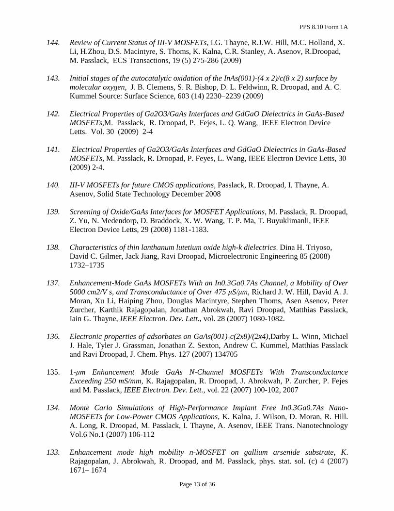
144. Review of Current Status of III-V MOSFETs, I.G. Thayne, R.J.W. Hill, M.C. Holland, X.
Li, H.Zhou, D.S. Macintyre, S. Thoms, K. Kalna, C.R. Stanley, A. Asenov, R.Droopad,
M. Passlack, ECS Transactions, 19 (5) 275-286 (2009)
143. Initial stages of the autocatalytic oxidation of the InAs(001)-(4 x 2)/c(8 x 2) surface by
molecular oxygen, J. B. Clemens, S. R. Bishop, D. L. Feldwinn, R. Droopad, and A. C.
Kummel Source: Surface Science, 603 (14) 2230–2239 (2009)
142. Electrical Properties of Ga2O3/GaAs Interfaces and GdGaO Dielectrics in GaAs-Based
MOSFETs,M. Passlack, R. Droopad, P. Fejes, L. Q. Wang, IEEE Electron Device
Letts. Vol. 30 (2009) 2-4
141. Electrical Properties of Ga2O3/GaAs Interfaces and GdGaO Dielectrics in GaAs-Based
MOSFETs, M. Passlack, R. Droopad, P. Feyes, L. Wang, IEEE Electron Device Letts, 30
(2009) 2-4.
140. III-V MOSFETs for future CMOS applications, Passlack, R. Droopad, I. Thayne, A.
Asenov, Solid State Technology December 2008
139. Screening of Oxide/GaAs Interfaces for MOSFET Applications, M. Passlack, R. Droopad,
Z. Yu, N. Medendorp, D. Braddock, X. W. Wang, T. P. Ma, T. Buyuklimanli, IEEE
Electron Device Letts, 29 (2008) 1181-1183.
138. Characteristics of thin lanthanum lutetium oxide high-k dielectrics, Dina H. Triyoso,
David C. Gilmer, Jack Jiang, Ravi Droopad, Microelectronic Engineering 85 (2008)
1732–1735
137. Enhancement-Mode GaAs MOSFETs With an In0.3Ga0.7As Channel, a Mobility of Over
5000 cm2/V s, and Transconductance of Over 475 μS/μm, Richard J. W. Hill, David A. J.
Moran, Xu Li, Haiping Zhou, Douglas Macintyre, Stephen Thoms, Asen Asenov, Peter
Zurcher, Karthik Rajagopalan, Jonathan Abrokwah, Ravi Droopad, Matthias Passlack,
Iain G. Thayne, IEEE Electron. Dev. Lett., vol. 28 (2007) 1080-1082.
136. Electronic properties of adsorbates on GaAs(001)-c(2x8)/(2x4),Darby L. Winn, Michael
J. Hale, Tyler J. Grassman, Jonathan Z. Sexton, Andrew C. Kummel, Matthias Passlack
and Ravi Droopad, J. Chem. Phys. 127 (2007) 134705
135. 1-μm Enhancement Mode GaAs N-Channel MOSFETs With Transconductance
Exceeding 250 mS/mm, K. Rajagopalan, R. Droopad, J. Abrokwah, P. Zurcher, P. Fejes
and M. Passlack, IEEE Electron. Dev. Lett., vol. 22 (2007) 100-102, 2007
134. Monte Carlo Simulations of High-Performance Implant Free In0.3Ga0.7As Nano-
MOSFETs for Low-Power CMOS Applications, K. Kalna, J. Wilson, D. Moran, R. Hill.
A. Long, R. Droopad, M. Passlack, I. Thayne, A. Asenov, IEEE Trans. Nanotechnology
Vol.6 No.1 (2007) 106-112
133. Enhancement mode high mobility n-MOSFET on gallium arsenide substrate, K.
Rajagopalan, J. Abrokwah, R. Droopad, and M. Passlack, phys. stat. sol. (c) 4 (2007)
1671– 1674

PPS 8.10 Form 1A
Page 14 of 36
132. Development of GaAs-based MOSFET using molecular beam epitaxy, Ravi Droopad,
Karthik Rajagopalan, Jon Abrokwah, Liz Adams, Nate England, Dave Uebelhoer, Peter
Fejes, Peter Zurcher, Matthias Passlack, Journal of Crystal Growth 301–302 (2007) 139–
144
131. Direct and indirect causes of Fermi level pinning at the SiO∕GaAs interface, Darby L.
Winn / Michael J. Hale / Tyler J. Grassman / Andrew C. Kummel / Ravi Droopad /
Matthias Passlack, The Journal of Chemical Physics, 126 (2007) 84703
130. 180nm metal gate, high-k dielectric,implant-free III–V MOSFETs with transconductance
of over 425 μS/μm, R.J.W. Hill, D.A.J. Moran, X. Li, H. Zhou, D. Macintyre, S. Thoms,
R. Droopad, M. Passlack and I.G. Thayne, Electronics Letts, 43 (2007) 543-545
129. Compound semiconductor MOSFETs, R. Droopad, K. Rajagopalan, J. Abrokwah, P.
Zurcher, M. Passlack, Microelectronic Engineering 84 (2007) 2138–2141
128. Gate dielectrics on compound semiconductors by molecular beam epitaxy, R. Droopad,
K. Rajagopalan, J. Abrokwah, , M. Passlack, J. Vac. Sci Technol. B24 (2006) 1479-
1482
127. In0.75Ga0.25As channel layers with record mobility exceeding 12,000 cm2/Vs for use in
high-k dielectric NMOSFETs, R. Droopad, K. Rajagopalan, J. Abrokwah, M. Canonico ,
M. Passlack, Solid State Electronics, 50 (2006) 1175
126. Electron energy barriers at interfaces of GaAs(001) with LaAlO3 and Gd2O3, V. V.
Afanasev, A. Stesmans, R, Droopad, M. Passlack, L. F. Edge, D. G. Schlom, Appl. Phys.
Lett. 89 (2006) 092103
125. Implant-Free high-Mobility Flatband MOSFET: Principles of Operation, M. Passlack, K.
Rajagopalan, J. Abrokwah, R. Droopad, IEEE Trans. Elect. Dev. 53 (2006) 2454
124. Enhancement-Mode GaAs n-Channel MOSFET, K. Rajagopalan, J. Abrokwah, R.
Droopad, M. Passlack, IEEE Electron. Dev. Lett., vol. 27, no. 12, pp. 959-962, 2006
123. High mobility III-V MOSFET technology, Passlack, M.; Droopad, R.; Rajagopalan, K.;
Abrokwah, J.; Zurcher, P.; Fejes, P., 2006 IEEE Compound Semiconductor Integrated
Circuit Symposium (IEEE Cat. No.06CH37760) p.4 pp. 2006
122. Gallium oxide (Ga2 O3) on gallium arsenide-A low defect, high-K system for future
devices, Paterson, G.W. / Wilson, J.A. / Moran, D. / Hill, R. / Long, A.R. / Thayne, I. /
Passlack, M. / Droopad, R., Materials Science & Engineering B, 135 (2006) 277-81
121. Gate dielectrics on compound semiconductors, R. Droopad, M. Passlack, N. England,
K. Rajagopalan, J. Abrokwah, A. Kummel, Microelectronic Engineering, 80 (2005),
138-145
PPS 8.10 Form 1A
Page 15 of 36
120. Chemically resolved scanning tunneling microscopy imaging of Al on p-type
AlGaAs(001) c(2×8)∕(2×4), M. J. Hale, D. L. Winn, T. J. Grassman, A. C. Kummel, R.
Droopad, The Journal of Chemical Physics, Mar 2005
119. High Mobility NMOSFET Structure with High-k Dielectric, M. Passlack, R. Droopad, K.
Rajagopalan, J. Abrokwah, R. Gregory, D. Nguyen, IEEE Electron. Dev. Lett., vol. 26,
no. 10, pp. 713-715, 2005.
118. Epitaxial Pb(Zr,Ti)O/sub 3/ capacitors on Si by liquid delivery metalorganic chemical
vapor deposition, Yang, S.Y., Liu, B.T., Ouyang, J., Nagarajan, V., Kulkarni, V.N.,
Ramesh, R., Kidder, J., Droopad, R., Eisenbeiser, K., Journal of Electroceramics vol.14,
no.1 p.37-44 Jan. 2005
117. X-ray absorption fine-structure determination of interfacial polarization in SrTiO3 thin
films grown on Si(001), J C Woicik / F S Aguirre-Tostada / A Herrera-Gomez / R
Droopad / Z Yu / D Schlom / E Karapetrova / Zschack, P / P Pianetta, Physica Scripta,
2005, no.T115 (2005) 3
116. Epitaxial BiFeO/sub 3/ thin films on Si, Wang, J.; Zheng, H.; Ma, Z.; Prasertchoung, S.;
Wuttig, M.; Droopad, R.; Yu, J.; Eisenbeiser, K.; Ramesh, R. Applied Physics Letters
vol.85, no.13 p.2574-6 27 Sept. 2004
115. Heteroepitaxy of SrTiO/sub 3/ on vicinal Si(001): growth and kinetic effects, Liang, Y.;
Wei, Y.; Hu, X.M.; Yu, Z.; Droopad, R.; Li, H.; Moore, K., Journal of Applied Physics
vol.96, no.6 p.3413-16 15 Sept. 2004
114. Hetero-epitaxy of perovskite oxides on GaAs(001) by molecular beam epitaxy, Liang, Y.;
Kulik, J.; Eschrich, T.C.; Droopad, R.; Yu, Z.; Maniar, P., Applied Physics Letters
vol.85, no.7 p.1217-19 16 Aug. 2004
113. Displacive phase transition in SrTiO/sub 3/ thin films grown on Si(001), Aguirre-
Tostado, F.S.; Herrera-Gomez, A.; Woicik, J.C.; Droopad, R.; Yu, Z.; Schlom, D.G.;
Karapetrova, J.; Zschack, P.; Pianetta, P., Journal of Vacuum Science & Technology A
(Vacuum, Surfaces, and Films) vol.22, no.4 p.1356-60 July 2004
112. High-performance carbon nanotube transistors on SrTiO/sub 3//Si substrates, Kim,
B.M.; Brintlinger, T.; Cobas, E.; Fuhrer, M.S.; Haimei Zheng; Yu, Z.; Droopad, R.;
Ramdani, J.; Eisenbeiser, K., Applied Physics Letters vol.84, no.11 p.1946-8 15 March
2004
111. Colossal magnetoresistive manganite-based ferroelectric field-effect transistor on Si,
Zhao, T.; Ogale, S.B.; Shinde, S.R.; Ramesh, R.; Droopad, R.; Yu, J.; Eisenbeiser, K.;
Misewich, J., Applied Physics Letters vol.84, no.5 p.750-2 2 Feb. 2004
110. Elastic anomaly for SrTiO3 thin films grown on Si(001), F. S. Aguirre-Tostado, A.
Herrera-Gómez, J. C. Woicik, R. Droopad, Z. Yu, D. G. Schlom, P. Zschack, E.
Karapetrova, P. Pianetta, and C. S. Hellberg, PHYSICAL REVIEW B 70, 201403(R)
(2004)
PPS 8.10 Form 1A
Page 16 of 36
109. Development of integrated heterostructures on silicon by MBE, Droopad, R., Zhiyi Yu,
Hao Li, Yong Liang, Overgaard, C., Demkov, A., Xiaodong Zhang, Moore, K.,
Eisenbeiser, K., Hu, M., Curless, J., Finder, J., Journal of Crystal Growth vol.251,
(2003) 638-44
108. Crystalline Oxide-based Devices on Silicon Substrate, K. Eisenbeiser, R. Droopad, Z.
Yu, C. Overgaard, J. Kulik, J. Finder, S. M. Smith, S. Voight, D. Penunuri, J. Electronic
Materials, Vol 32 (2003) 868-871
107. Growth and physical properties of Ga/sub 2/O/sub 3/ thin films on GaAs(001) substrate
by molecular-beam epitaxy, Yu, Z., Overgaard, C.D., Droopad, R., Passlack, M.,
Abrokwah, J.K., Applied Physics Letters 82, (2003) 2978-80
106. Two-dimensional growth of high-quality strontium titanate thin films on Si, Li, H.; Hu,
X.; Wei, Y.; Yu, Z.; Zhang, X.; Droopad, R.; Demkov, A.A.; Edwards, J.; Moore, K.;
Ooms, W.; Kulik, J.; Fejes, P., Journal of Applied Physics vol.93, no.8 p.4521-5 15 April
2003
105. Thermally induced oxide crystallinity and interface destruction in Ga/sub 2/O/sub 3/-
GaAs structures, Passlack, M.; Abrokwah, J.K.; Yu, Z.; Droopad, R.; Overgaard, C.;
Kawayoshi, H., Applied Physics Letters vol.82, no.11 p.1691-3 17 March 2003
104. The interface of epitaxial SrTiO/sub 3/ on silicon: in situ and ex situ studies, Xiaoming
Hu; Li, H.; Liang, Y.; Wei, Y.; Yu, Z.; Marshall, D.; Edwards, J.; Droopad, R.; Zhang,
X.; Demkov, A.A.; Moore, K.; Kulik, J., Applied Physics Letters vol.82, no.2 p.203-5 13
Jan. 2003
103. GaAs on silicon Using an Oxide Buffer Layer, R. Droopad, J. Curless, Z. Yu, D. Jordan,
Y. Liang, C. Overgaard, H. Li, T. Eschrich, J. Ramdani, L. hilt, B. Craigo, K.
Eisenbeiser, J. Kulik, P. Feyes, J. Finder, X. Hu, Y. Wei, J. Edwards, K. Moore, M.
O’Steen, O. Baklenov, Inst. Phys. Conf, Ser. No 174 p. 1-8 (2003)
102. Progress in epitaxial oxides on semiconductors, Yu, Z.; Liang, Y.; Hi, H.; Curless, J.;
Overgaard, C.; Droopad, R.; Wei, Y.; Hu, X.; Craigo, B.; Finder, J.; Eisenbeiser, K.;
Talin, A.; Smith, S.; Voight, S.; Wang, J.; Marshall, D.; Jordan, D.; Edwards, J., Jr.;
Moore, K.; , Crystalline Oxide-Silicon Heterostructures and Oxide Optoelectronics.
Symposium (Mater. Res. Soc. Symposium Proceedings Vol.747) p.31-42 2003
101. Mechanism of cleaning Si(100) surface using Sr or SrO for the growth of crystalline
SrTiO3 films, Yi Wei, Xiaoming Hu, Yong Liang, Jordan, D.C., Craigo, B., Droopad, R.,
Yu, Z., Demkov, A., Edwards, J.L., Jr., Ooms, W.J., Journal of Vacuum Science &
Technology B (Microelectronics and Nanometer Structures) 20, (2002)1402-5
100. Si(100) surface cleaning using Sr and SrO, Yi Wei, Xiaoming Hu, Yong Liang, Jordan,
D.C., Craigo, B., Droopad, R., Yu, Z., Demkov, A., Edwards, J.L., Jr., Moore, K., Ooms,
W.J., Silicon Materials - Processing, Characterization and Reliability Symposium
(Mater. Res. Soc. Proceedings Vol. 716) (2002)139-44
PPS 8.10 Form 1A
Page 17 of 36
99. Sr/Si template formation for the epitaxial growth of SrTiO/sub 3/ on silicon, Xiaoming
Hu, Liang, Y., Yi Wei, Edwards, J.L., Jr., Droopad, R., Moore, K., Ooms, W.J.,Silicon
Materials - Processing, Characterization and Reliability Symposium (Mater. Res. Soc.
Proceedings Vol. 716) (2002) 261-6
98. Development of integrated heterostructures on silicon by MBE, Droopad, R., Curless,
J.A., Yu, Z., Jordan, D.C., Liang, Y., Overgaard, C.D., Li, H., Eschrich, T., Craigo, B.,
Eisenbeiser, K.W., Finder, J., Hu, X., Wei, Y., Edwards, J., Ramdani, J., Tisinger, L.,
Demkov, A., Moore, K., Marshall, D., Ooms, W.J., Prendergast, J, J. Crys. Growth Vol
251 (2003) 638-644
97. Development of integrated heterostructures on silicon by MBE, Droopad, R., Curless,
J.A., Yu, Z., Jordan, D.C., Liang, Y., Overgaard, C.D., Li, H., Eschrich, T., Craigo, B.,
Eisenbeiser, K.W., Finder, J., Hu, X., Wei, Y., Edwards, J., Ramdani, J., Tisinger, L.,
Demkov, A., Moore, K., Marshall, D., Ooms, W.J., Prendergast, J, 2002 International
Conference on Molecular Beam Epitaxy (Cat. No.02EX607) p.45-6 2002
96. Realizing intrinsic piezoresponse in epitaxial submicron lead zirconate titanate
capacitors on Si, Nagarajan, V., Stanishevsky, A., Chen, L., Zhao, T., Liu, B.-T.,
Melngailis, J., Roytburd, A.L., Ramesh, R., Finder, J., Yu, Z., Droopad, R., Eisenbeiser,
K., Applied Physics Letters 81, (2002)4215-17
95. New research yields epitaxially grown GaAs on Si, Eisenbeiser, K., Droopad, R., Finder,
J., Solid State Technology 45, (2002) 61-2, 64, 67
94. Self-aligned GaAs p-channel enhancement mode MOS heterostructure field-effect
transistor, Passlack, M., Abrokwah, J.K., Droopad, R., Zhiyi Yu, Overgaard, C., Sang In
Yi, Hale, M., Sexton, J., Kummel, A.C., IEEE Electron Device Letters 23, (2002) 508-10
93. Materials and physical properties of novel high-k and medium-k gate dielectrics, Liu, R.,
Zollner, S., Fejes, P., Gregory, R., Lu, S., Reid, K., Gilmer, D., Nguyen, B.-Y., Yu, Z.,
Droopad, R., Curless, J., Demkov, A., Finder, J., Eisenbeiser, K., Gate Stack and Silicide
Issues in Silicon Processing II. Symposium (Materials Research Society Symposium
Proceedings Vol.670) (2002) 1-12
92. GaAs-based heterostructures on silicon, Yu, Z., Droopad, R., Jordan, D., Curless, J.,
Liang, Y., Overgaard, C., Li, H., Talin, A., Eschrich, T., Craigo, B., Eisenbeiser, K.,
Emrick, R., Finder, J., Hu, X., Wei, Y., Edwards, J., Jr., Convey, D., Moore, K.,
Marshall, D., Ramdani, J., Tisinger, L., 2002 GaAs MANTECH Conference. Digest of
Papers p.276-9 2002
91. Direct observation of atomic disordering at the SrTiO/sub 3//Si interface due to oxygen
diffusion, Shutthanandan, V., Thevuthasan, S., Liang, Y., Adams, E.M., Yu, Z.,
Droopad, R., Applied Physics Letters 80, (2002) 1803-5
90. GaAs MESFETs fabricated on Si substrates using a SrTiO/sub 3/ buffer layer,
Eisenbeiser, K., Emrick, R., Droopad, R., Yu, Z., Finder, J., Rockwell, S., Holmes, J.,
Overgaard, C., Ooms, W., IEEE Electron Device Letters 23, (2002) 300-2

PPS 8.10 Form 1A
Page 18 of 36
89. Passivation of defects at the SrTiO/sub 3//Si interface with H and H/sub 2/, Browne,
R.J., Ogryzlo, E.A., Eisenbeiser, K., Yu, Z., Droopad, R., Overgaard, C., Applied
Physics Letters 80, (2002) 2699-700
88. Study of microstructure in SrTiO/sub 3//Si by high-resolution transmission electron
microscopy, Yang, G.Y., Finder, J.M., Wang, J., Wang, Z.L., Yu, Z., Ramdani, J.,
Droopad, R., Eisenbeiser, K.W., Ramesh, R., Journal of Materials Research 17, (2002)
204-13
87. Epitaxial ferroelectric Pb(Zr, Ti)O/sub 3/ thin films on Si using SrTiO/sub 3/ template
layers, Wang, Y., Ganpule, C., Liu, B.T., Li, H., Mori, K., Hill, B., Wuttig, M., Ramesh,
R., Finder, J., Yu, Z., Droopad, R., Eisenbeiser, K., Applied Physics Letters 80, (2002)
97-9
86. Materials and physical properties of novel high-k and medium-k gate dielectrics, Liu, R.;
Zollner, S.; Fejes, P.; Gregory, R.; Lu, S.; Reid, K.; Gilmer, D.; Nguyen, B.-Y.; Yu, Z.;
Droopad, R.; Curless, J.; Demkov, A.; Finder, J.; Eisenbeiser, K.; Campbell, S.A.;
Clevengr, L.A.; Griffin, P.B.; Hobbs, C.C., Gate Stack and Silicide Issues in Silicon
Processing II. Symposium (Materials Research Society Symposium Proceedings
Vol.670) p.K1.1.1-12 2002
85. Photoemission from the Sr/Si(001) interface, Herrera-Gómez, A.; Aguirre-Tostado, F. S.;
Sun, Y.; Pianetta, P.; Yu, Z.; Marshall, D.; Droopad, R.; Spicer, W. E., , Journal of
Applied Physics, Volume 90, Issue 12, pp. 6070-6072 (2001).
84. Band offset and structure of SrTiO3 /Si(001) heterojunctions, Chambers, S. A.; Liang, Y.;
Yu, Z.; Droopad, R.; Ramdani, J., Journal of Vacuum Science & Technology A:
Vacuum, Surfaces, and Films, Volume 19, Issue 3, May 2001, pp.934-939
83. Development of high dielectric constant epitaxial oxides on silicon by molecular beam
epitaxy, R. Droopad, Z. Yu, J. Ramdani, L. Hilt, J. Curless, C. Overgaard, J. L. Edwards,
Jr , J. Finder, K. Eisenbeiser and W. Ooms, Materials Science & Engineering B (Solid-
State Materials for Advanced Technology) vol.B87, no.3 p.292-6 19 Dec. 2001
82. Comparative study of Sr and Ba adsorption on Si(100), Xiaoming Hu, Z. Yu, J. A.
Curless, R. Droopad, K. Eisenbeiser, J. L. Edwards, Jr., W. J. Ooms and D. Sarid,
Applied Surface Science vol.181, no.1-2 p.103-10 3 Sept. 2001
81. Epitaxial oxides on silicon by molecular beam epitaxy, Ravi Droopad, Zhiyi Yu, Jamal
Ramdani, Lyndee Hilt, Jay Curless, Corey Overgaard, John L. Edwards, Jeff Finder, Kurt
Eisenbeiser, Jun Wang, V. Kaushik, B-Y Ngyuen and Bill Ooms, J. Crystal Growth, 227-
228 (2001) 936-943
80. Band discontinuities at epitaxial SrTiO3/Si(001) heterojunctions, Chambers, S. A.;
Liang, Y.; Yu, Z.; Droopad, R.; Ramdani, J.; Eisenbeiser, K., Applied Physics Letters,
Volume 77, Issue 11, September 11, 2000, pp.1662-1664
79. Optical properties of bulk and thin-film SrTiO3 on Si and Pt, Zollner, Stefan;
Demkov, A. A.; Liu, R.; Fejes, P. L.; Gregory, R. B.; Alluri, Prasad; Curless, J. A.;

PPS 8.10 Form 1A
Page 19 of 36
Yu, Z.; Ramdani, J.; Droopad, R.; Tiwald, T. E.; Hilfiker, J. N.; Woollam, J. A. Journal
of Vacuum Science & Technology B: Microelectronics and Nanometer Structures,
Volume 18, Issue 4, July 2000, pp.2242-2254
78. Epitaxial oxide thin films on Si(001), Yu, Z.; Ramdani, J.; Curless, J. A.;
Overgaard, C. D.; Finder, J. M.; Droopad, R.; Eisenbeiser, K. W.; Hallmark, J. A.;
Ooms, W. J.; Kaushik, V. S. Journal of Vacuum Science & Technology B:
Microelectronics and Nanometer Structures, Volume 18, Issue 4, July 2000, pp.2139-
2145
77. Epitaxial perovskite thin films grown on silicon by molecular beam epitaxy, Yu, Z.;
Ramdani, J.; Curless, J. A.; Finder, J. M.; Overgaard, C. D.; Droopad, R.;
Eisenbeiser, K. W.; Hallmark, J. A.; Ooms, W. J.; Conner, J. R.; Kaushik, V. S. Journal
of Vacuum Science & Technology B: Microelectronics and Nanometer Structures,
Volume 18, Issue 3, May 2000, pp.1653-1657
76. Field effect transistors with SrTiO3 gate dielectric on Si, Eisenbeiser, K.; Finder, J. M.;
Yu, Z.; Ramdani, J.; Curless, J. A.; Hallmark, J. A.; Droopad, R.; Ooms, W. J.;
Salem, L.; Bradshaw, S.; Overgaard, C. D. Applied Physics Letters, Volume 76, Issue 10,
March 6, 2000, pp.1324-1326
75. The (3*2) phase of Ba adsorption on Si(001)-2*1, Hu, X.; Yao, X.; Peterson, C.A.; Sarid,
D.; Yu, Z.; Wang, J.; Marshall, D.S.; Droopad, R.; Hallmark, J.A.; Ooms, W.J., Surface
Science vol.445, no.2-3 p.256-66 20 Jan. 2000
74. Optical properties of thin-film SrTiO/sub 3/ on Si grown by MBE, Zollner, S.; Demkov,
A.A.; Liu, R.; Curless, J.A.; Yu, Z.; Ramdani, J.; Droopad, R., Recent Developments in
Oxide and Metal Epitaxy - Theory and Experiment. Symposium (Materials Research
Society Symposium Proceedings Vol.619) p.167-71 2000
73. Epitaxial oxide films on silicon: growth, modeling and device properties, Droopad, R.;
Wang, J.; Eisenbeiser, K.; Yu, Z.; Ramdani, J.; Curless, J.A.; Overgaard, C.D.; Finder,
J.M.; Hallmark, J.A.; Kaushik, V.; Nguyen, B.Y.; Marshall, D.S.; Ooms, W.J., Recent
Developments in Oxide and Metal Epitaxy - Theory and Experiment. Symposium
(Materials Research Society Symposium Proceedings Vol.619) p.155-65 2000
72. Interface characterization of high-quality SrTiO/sub 3/ thin films on Si(100) substrates
grown by molecular beam epitaxy, Ramdani, J.; Droopad, R.; Yu, Z.; Curless, J.A.;
Overgaard, C.D.; Finder, J.; Eisenbeiser, K.; Hallmark, J.A.; Ooms, W.J.; Kaushik, V.;
Alluri, P.; Pietambaram, S., Applied Surface Science vol.159-160 p.127-33 June 2000
71. Barium adsorption on Si(100)-(2*1) at room temperature: a bi-polar scanning tunneling
microscopy study, Hu, X.; Yao, X.; Peterson, C.A.; Sarid, D.; Yu, Z.; Wang, J.; Marshall,
D.S.; Curless, J.A.; Ramdani, J.; Droopad, R.; Hallmark, J.A.; Ooms, W.J., Surface
Science vol.457, no.1-2 p.L391-6 1 June 2000
70. Initial stages of Ba adsorption on the Si(100)-(2×1) surface at room temperature,
Yao, X.; Hu, Xiaoming; Sarid, D.; Yu, Z.; Wang, J.; Marshall, D. S.; Droopad, R.;

PPS 8.10 Form 1A
Page 20 of 36
Abrokwah, J. K.; Hallmark, J. A.; Ooms, W. J. Physical Review B (Condensed Matter
and Materials Physics), Volume 59, Issue 7, February 15, 1999, pp.5115-5119
69. Interface charge and nonradiative carrier recombination in Ga2O3-GaAs interface
structures, Passlack, M.; Yu, Z.; Droopad, R.; Bowers, B.; Overgaard, C.; Abrokwah, J.;
Kummel, A. C. Journal of Vacuum Science & Technology B: Microelectronics and
Nanometer Structures, Volume 17, Issue 1, January 1999, pp.49-52
68. Metamorphic InAlAs/InGaAs enhancement mode HEMTs on GaAs substrates,
Eisenbeiser, K.; Droopad, R.; Jenn-Hwa Huang, IEEE Electron Device Letters vol.20,
no.10 p.507-9 Oct. 1999
67. Phases of Ba adsorption on Si(100)-(2*1) studied by LEED and AES, Xiaoming Hu;
Peterson, C.A.; Sarid, D.; Yu, Z.; Wang, J.; Marshall, D.S.; Droopad, R.; Hallmark, J.A.;
Ooms, W.J., Surface Science vol.426, no.1 p.69-74 3 May 1999
66. Properties of epitaxial SrTiO/sub 3/ thin films grown on silicon by molecular beam
epitaxy, Yu, Z.; Droopad, R.; Ramdani, J.; Curless, J.A.; Overgaard, C.D.; Finder, J.M.;
Eisenbeiser, K.W.; Wang, J.; Hallmark, J.A.; Ooms, W.J.; Huff, H.R.; Richter, C.A.;
Green, M.L.; Lucovsky, G.; Hattori, T., Ultrathin SiO/sub 2/ and High-K Materials for
ULSI Gate Dielectrics. Symposium p.427-33 1999
65. Epitaxial BaTiO/sub 3/ films on silicon for MFSFFT applications, Hallmark, J.; Zhiyi
Yu; Droopad, R.; Ramdani, J.; Curless, J.; Overgaard, C.; Finder, J.; Marshall, D.; Jun
Wang; Ooms, B., Integrated Ferroelectrics vol.27, no.1-4 p.41-50 1999
64. Nonradiative recombination at GaAs homointerfaces fabricated using an As cap
deposition/removal process, Passlack, M.; Droopad, R.; Yu, Z.; Overgaard, C.;
Bowers, B.; Abrokwah, J. Applied Physics Letters, Volume 72, Issue 24, June 15, 1998,
pp.3163-3165
63. Electronic properties of MBE grown GaAs homointerfaces fabricated using the As cap
deposition/removal technique, Passlack, M.; Droopad, R.; Yu, Z.; Overgaard, C.; Bowers,
B.; Abrokwah, J.; Melloch, M.; Reed, M.A., Compound Semiconductors 1997.
Proceedings of the IEEE Twenty-Fourth International Symposium on Compound
Semiconductors p.131-4 1998
62. Device and process optimization for a low voltage enhancement mode power
heterojunction FET for portable applications, Huang, J.H.; Glass, E.; Abrokwah, J.;
Bernhardt, B.; Majerus, M.; Spears, E.; Parsey, J.M., Jr.; Scheitlin, D.; Droopad, R.;
Mills, L.A.; Hawthorne, K.; Blaugh, J., GaAs IC Symposium. IEEE Gallium Arsenide
Integrated Circuit Symposium. 19th Annual Technical Digest 1997 (Cat.
No.97CH36098) p.55-8 1997
61. A true enhancement mode single supply power HFET for portable applications, Glass,
E.; Huang, J.-H.; Abrokwah, J.; Bernhardt, B.; Majerus, M.; Spears, E.; Droopad, R.;
Ooms, B.; Koepf, G.A., 1997 IEEE MTT-S International Microwave Symposium Digest
(Cat. No.97CH36037) p.1399-402 vol.3 1997

PPS 8.10 Form 1A
Page 21 of 36
60. A vertical-cavity surface-emitting laser appliqued to a 0.8- mu m NMOS driver, Mathine,
D.L.; Droopad, R.; Maracas, G.N., IEEE Photonics Technology Letters vol.9, no.7 p.869-
71 July 1997
59. Contactless electroreflectance characterization of three InGaAs quantum wells placed in
a GaAs/AlGaAs resonant cavity, Moneger, S.; Qiang, H.; Pollak, F.H.; Mathine, D.L.;
Droopad, R.; Maracas, G.N., Solid-State Electronics vol.39, no.6 p.871-4 June 1996
58. Reduction of the thermal impedance of vertical-cavity surface-emitting lasers after
integration with copper substrates, Mathine, D. L.; Nejad, H.; Allee, D. R.; Droopad, R.;
Maracas, G. N. Applied Physics Letters, Volume 69, Issue 4, July 22, 1996, pp.463-464
57. Ellipsometry for III-V epitaxial growth diagnostics, Maracas, G. N.; Kuo, C. H.;
Anand, S.; Droopad, R.; Sohie, G. R. L.; Levola, T. Journal of Vacuum Science &
Technology A: Vacuum, Surfaces, and Films, Volume 13, Issue 3, May 1995, pp.727-
732
56. Integration of a single vertical-cavity surface emitting laser onto a CMOS inverter chip,
Daryanani, S.; Fathollahnejad, H.; Mathine, D. L.; Droopad, R.; Kubes, A.;
Maracas, G. N. Electronics Letters (ISSN 0013-5194), vol. 31, no. 10, p. 833-834
55. Measurement of AlxGa1 - xAs temperature dependent optical constants by spectroscopic
ellipsometry, Kuo, C. H.; Anand, S.; Fathollahnejad, H.; Ramamurti, R.; Droopad, R.;
Maracas, G. N. Journal of Vacuum Science & Technology B: Microelectronics and
Nanometer Structures, Volume 13, Issue 2, March 1995, pp.681-684
54. Temperature-dependent pseudodielectric functions of GaAs determined by spectroscopic
ellipsometry, Maracas, G. N.; Kuo, C. H.; Anand, S.; Droopad, R. Journal of Applied
Physics (ISSN 0021-8979), vol. 77, no. 4, p. 1701-1704
53. The integration of GaAs vertical-cavity surface emitting lasers onto silicon circuitry,
Fathollahnejad, H.; Daryanani, S.; Mathine, D.L.; Chuang, C.P.; Droopad, R.; Maracas,
G.N., Proceedings. IEEE/Cornell Conference on Advanced Concepts in High Speed
Semiconductor Devices and Circuits (Cat. No.95CH35735) p.373-81 1995
52. Real time monitoring of III-V alloy composition and real time control of quantum well
thickness in MBE by multi-wavelength ellipsometry, Chau-Hong Kuo; Anand, S.;
Droopad, R.; Mathine, D.L.; Maracas, G.N.; Johs, B.; He, P.; Woollam, J.A.; Levola, T.;
Goronkin, H.; Mishra, U., Compound Semiconductors 1994. Proceedings of the Twenty-
First International Symposium p.29-34 1995
51. Low resistance Pd/Ge ohmic contacts to epitaxially lifted-off n-type GaAs film,
Fathollahnejad, H.; Rajesh, R.; Liu, J.; Droopad, R.; Maracas, G.N.; Carpenter, R.W.,
Journal of Electronic Materials vol.24, no.1 p.35-8 Jan. 1995
50. Lattice-constant dependence of the dynamical effective charge in AlAs and GaAs,
Spencer, G. S.; Ho, A. C.; Menéndez, J.; Droopad, R.; Fathollahnejad, H.; Maracas, G. N.

PPS 8.10 Form 1A
Page 22 of 36
Physical Review B (Condensed Matter), Volume 50, Issue 19, November 15, 1994,
pp.14125-14130
49. High-field electron transport in GaAs: a picosecond time-resolved Raman probe,
Grann, Erik D.; Sheih, Shou J.; Chia, C.; Tsen, Kong T.; Sankey, Otto F.;
Maracas, George N.; Droopad, R.; Salvador, A.; Botcharev, A.; Morkoc, Hadis Proc.
SPIE Vol. 2142, p. 190-197, Ultrafast Phenomena in Semiconductors, David K. Ferry;
Henry M. van Driel; Eds.
48. Photoreflectance study of GaAs/GaAlAs digital alloy compositionally graded structures,
Qiang, Hao; Pollak, Fred H.; Huang, Y.-S.; Chi, W. S.; Droopad, R.; Mathine, David L.;
Maracas, George N. Proc. SPIE Vol. 2139, p. 11-19, Quantum Well and Superlattice
Physics V, Gottfried H. Doehler; Emil S. Koteles; Eds.
47. Characterization of an AlGaAs/GaAs asymmetric triangular quantum well grown by a
digital alloy approximation, Mathine, D. L.; Maracas, G. N.; Gerber, D. S.; Droopad, R.;
Graham, R. J.; McCartney, M. R. Journal of Applied Physics, Volume 75, Issue 9, May
1, 1994, pp.4551-4556
46. Measurement of GaAs temperature-dependent optical constants by spectroscopic
ellipsometry, Kuo, C. H.; Anand, S.; Droopad, R.; Choi, K. Y.; Maracas, G. N. Journal of
Vacuum Science & Technology B: Microelectronics and Nanometer Structures, Volume
12, Issue 2, March 1994, pp.1214-1216
45. Determination of molecular beam epitaxial growth parameters by ellipsometry,
Droopad, R.; Kuo, C. H.; Anand, S.; Choi, K. Y.; Maracas, G. N. Journal of Vacuum
Science & Technology B: Microelectronics and Nanometer Structures, Volume 12, Issue
2, March 1994, pp.1211-1213
44. Application of the digital alloy composition grading technique to strained
InGaAs/GaAs/AlGaAs diode laser active regions, Cody, Jeffrey G.; Mathine, David L.;
Droopad, Ravi; Maracas, George N.; Rajesh, Ramamurti; Carpenter, Ray W. Journal of
Vacuum Science & Technology B: Microelectronics and Nanometer Structures, Volume
12, Issue 2, March 1994, pp.1075-1077
43. Picosecond Raman studies of electric-field-induced nonequilibrium carrier distributions
in GaAs-based p-i-n nanostructure semiconductors, Grann, E. D.; Sheih, S. J.; Chia, C.;
Tsen, K. T.; Sankey, O. F.; Guncer, Selim E.; Ferry, D. K.; Maracas, G.; Droopad, Ravi;
Salvador, A.; Botcharev, A.; Morkoç, H. Applied Physics Letters, Volume 64, Issue 10,
March 7, 1994, pp.1230-1232
42. Second-order Raman spectroscopy of AlAs: A test of lattice-dynamical models,
Spencer, G. S.; Grant, J.; Gray, R.; Zolman, J.; Menéndez, J.; Droopad, R.;
Maracas, G. N. Physical Review B (Condensed Matter), Volume 49, Issue 8, February
15, 1994, pp.5761-5764
41. Electroreflectance characterization of three InGaAs quantum wells placed in a
GaAs/GaAlAs resonant cavity: contactless and contact modes, Moneger, S.; Pollak, F.H.;
Mathine, D.L.; Droopad, R.; Maracas, G.N., LEOS '94. Conference Proceedings. IEEE

PPS 8.10 Form 1A
Page 23 of 36
Lasers and Electro-Optics Society 1994 7th Annual Meeting (Cat. No.94CH3371-2)
p.218-19 vol.2 1994
40. Electrical characterization of highly strained ultrathin InAs/GaAs quantum wells, Yu, F.;
Droopad, R.; Maracas, G.N.; Liu, J.; Rajesh, R.; Carpenter, R.W.; Gumbs, G.; Luryi, S.;
Weiss, B.; Wicks, G.W., Growth, Processing, and Characterization of Semiconductor
Heterostructures. Symposium p.151-6 1994
39. InGaAs quantum well vertical-cavity surface-emitting lasers integration onto silicon
substrates, Mathine, D.L.; Fathollahnejad, H.; Droopad, R.; Daryanani, S.; Maracas,
G.N., LEOS '94. Conference Proceedings. IEEE Lasers and Electro-Optics Society 1994
7th Annual Meeting (Cat. No.94CH3371-2) p.282-3 vol.1 1994
38. Vertical-cavity surface-emitting lasers integrated onto silicon substrates by PdGe
contacts, Fathollahnejad, H.; Mathine, D.L.; Droopad, R.; Maracas, G.N.; Daryanani, S.,
Electronics Letters vol.30, no.15 p.1235-6 21 July 1994
37. Comparison of electroabsorption in asymmetric triangular and rectangular GaAs/AlxGa1
- xAs multiple quantum wells, Gerber, D. S.; Droopad, R.; Maracas, G. N. Applied Physics
Letters, Volume 62, Issue 5, February 1, 1993, pp.525-527
36. In-situ spectroscopic ellipsometry in molecular beam epitaxy, Maracas, George N.;
Edwards, John L.; Shiralagi, K.; Choi, K. Y.; Droopad, R.; Johs, Blaine;
Woollam, John A. In Nebraska Univ., Materials, Structures, and Devices for High-Speed
Electronics 1 p
35. Real-time analysis of in-situ spectroscopic ellipsometric data during MBE growth of III-
V semiconductors, Johs, Blaine; Edwards, John L.; Shiralagi, K. T.; Droopad, R.;
Choi, K. Y.; Maracas, George N.; Meyer, Duane; Cooney, Gerald T.; Woollam, John A.
In Nebraska Univ., Materials, Structures, and Devices for High-Speed Electronics 1 p
34. A GaAs/AlGaAs Asymmetric Fabry-Perot Reflection Modulator with Very High Contrast
Ratio, D. S. Gerber, R. Droopad, G. N. Maracas, Photonics Technology Letts. 5 (1993)
55-58.
33. Pseudomorphic InGaAs/GaAs and GaAs/AlGaAs asymmetric triangular quantum wells
grown by MBE for optoelectronic device applications, Droopad, R.; Gerber, D.S.; Choi,
C.; Maracas, G.N., Journal of Crystal Growth vol.127, no.1-4 p.606-10 Feb. 1993
32. In situ spectroscopic ellipsometry in molecular beam epitaxy, Maracas, G. N.;
Edwards, J. L.; Shiralagi, K.; Choi, K. Y.; Droopad, R.; Johs, B.; Woolam, J. A. Journal
of Vacuum Science & Technology A: Vacuum, Surfaces, and Films, Volume 10, Issue 4,
July 1992, pp.1832-1839
31. Enhancement of mobility in pseudomorphic FET's with up and down monolayers,
Goronkin, Herb; Shen, Jun; Tehrani, Saied; Droopad, Ravindranath; Maracas, George N.;
Legge, Ron N.; Zhu, X. T. Japanese Journal of Applied Physics, Part 1 (ISSN 0021-
4922), vol. 31, no. 7, July 1992, p. 2071-2074.

PPS 8.10 Form 1A
Page 24 of 36
30. Quantum well thickness effect on the deep-shallow duality of Si in AlGaAs/InGaAs
heterostructures, Shen, J.; Tehrani, S.; Goronkin, H.; Droopad, R.; Maracas, G. Journal
of Applied Physics, Volume 71, Issue 12, June 15, 1992, pp.5985-5988
29. Low temperature GaAs grown by gas source molecular beam epitaxy, Droopad, R.;
Shiralagi, K. T.; Puechner, R. A.; Choi, K. Y.; Maracas, G. N. Chemical beam epitaxy
and related growth techniques 1991; Proceedings of the 3rd International Conference
/ICCBE-3/, Oxford, England, Sept. 1-5, 1991. A92-40901 16-76) Journal of Crystal
Growth (ISSN 0022-0248), vol. 120, no. 1-4, May 1992, p. 200-205.
28. Electron mobility enhancement by confining optical phonons in GaAs/AlAs multiple
quantum wells, Theodore Zhu, X.; Goronkin, Herbert; Maracas, George N.;
Droopad, Ravi; Stroscio, Michael A. Applied Physics Letters, Volume 60, Issue 17, April
27, 1992, pp.2141-2143
27. Hydride cracker nozzle design for gas source molecular beam epitaxy, Shiralagi, K. T.;
Choi, K. Y.; Droopad, R.; Maracas, G. N.; Quinn, W. E. Journal of Vacuum Science &
Technology A: Vacuum, Surfaces, and Films, Volume 10, Issue 1, January 1992, pp.46-
50
26. Nonlinear Electroabsorption in Asymmetric Triangular Quantum Well Self-Electro Effect
Devices, Puechner, R. A.; Gerber, D. S.; Droopad, R.; Maracas, G. N. Journal of
Nonlinear Optical Physics and Materials, Volume 1, Issue 03, pp. 473-491 (1992).
25. A Novel Optically Bistable Multiple Quantum Well Phase Modulator, Chongdae Park,
Kumar T. Shiralagi, Ravi Droopad, George N. Maracas, Photonics Technology Letts,
Vol. 4, 1225-1227, 1992.
24. In-situ and ex-situ characterization of GaAs/AlAs quantum well structures using
spectroscopic ellipsometry, Edwards, J.L.; Maracas, G.N.; Shiralagi, K.T.; Choi, K.Y.;
Droopad, R., Journal of Crystal Growth vol.120, no.1-4 p.78-83 May 1992
23. Molecular beam epitaxial growth and optical properties of strained rectangular and
asymmetric triangular InGaAs quantum well structures, Droopad, R.; Puechner, R. A.;
Choi, K. Y.; Shiralagi, K. T.; Maracas, G. N. Journal of Crystal Growth (ISSN 0022-
0248), vol. 114, no. 3, Nov. 1991, p. 327-336.
22. Local Vibrational Mode Spectroscopy of Si donors and Be Acceptors in MBE InAs and
InSb Studied by Infrared Absorption and Raman Scattering, R. Adinall, R. Murray, R. C.
Newman, J. Wagner, S. D. Parker, R. L. Williams, R. Droopad, A. G. DeOliveira, I.
Ferguson, R. A. Stradling, Semicond. Sci. & Tech. 6 (1991) 147-154.
21. Optical Properties of a Single Strained InGaAs/GaAs Quantum Well Grown on Vicinal
GaAs Surfaces, R. Droopad, R. A. Puechner, K. T. Shiralagi, K. Y. Choi, G. N. Maracas,
", Appl. Phys. Lett. 58(16) (1991) 1771-1779.
20. Electrical and Optical Characterization of Gas Source and Solid Source MBE Low
Temperature Buffers, R. A. Puechner, D. A. Johnson, K. T. Shiralagi, D. S. Gerber, R.
Droopad, G. N. Maracas, J. Crystal Growth 111 (1991) 43-49.
PPS 8.10 Form 1A
Page 25 of 36
19. Optical Properties of Quantum Wells Grown Upon Gas Source Molecular Beam Epitaxy
Low Temperature Buffers, K. T. Shiralagi, R. A. Puechner, K. Y. Choi, R. Droopad, G.
N. Maracas, J. Appl. Phys. 69 (1991) 7942-7944.
18. Optical Properties of Strained Asymmetric Triangular InGaAs/GaAs Multiple Quantum
Wells, R. Droopad, K. Y. Choi, R. A. Puechner, K. T. Shiralagi, D. S. Gerber, G. N.
Maracas, Appl. Phys. Lett. 59 (1991) 2308-2310.
17. Molecular Beam Epitaxial Growth and Optical Properties of Strained Rectangular and
Asymmetric Triangular InGaAs Quantum Well Structures, R. Droopad, R. A. Puechner,
K. Y. Choi, K. T. Shiralagi, G. N. Maracas, J. Crystal Growth. 114 (1991) 327-336.
16. Enhancement of mobility in pseudomorphic FETs with up and down monolayers,
Goronkin, H.; Tehrani, S.; Droopad, R.; Maracas, G.N.; Shen, J.; Legge, R.N.; Zhu, X.T.,
IEEE Transactions on Electron Devices vol.38, no.12 p.2703 Dec. 1991
15. Real-time analysis of in-situ spectroscopic ellipsometric data during MBE growth of III-
V semiconductors, Johs, B.; Edwards, J.L.; Shiralagi, K.T.; Droopad, R.; Choi, K.Y.;
Maracas, G.N.; Meyer, D.; Cooney, G.T.; Woollam, J.A.; Kuech, T.F.; Dapkus, P.D.;
Aoyagi, Y., Atomic Layer Growth and Processing Symposium p.75-80 1991
14. Narrow photoluminescence linewidth of quantum wells grown by gas source molecular
beam epitaxy, Shiralagi, K.T.; Puechner, R.A.; Choi, K.Y.; Droopad, R.; Maracas, G.N.,
Journal of Crystal Growth vol.114, no.3 p.337-45 Nov. 1991
13. Optical Properties of Asymmetric Triangular Quantum Wells for Self Electro-optic Effect
Devices, R. A. Puechner, D. S. Gerber, D. A. Johnson, R. Droopad, G. N. Maracas, Proc.
IEEE Nonlinear Optics: Materials, Phenomena and Devices, Hawaii, (1990) Technical
Digest pg 115
12. Protective Overlayer Techniques for Preparation of InSb(001) Surfaces, S. D. Evans, L.
L. Cao, R. G. Egdell, R. Droopad, S. D. Parker, R. A. Stradling, Surf. Sci. 226 (1990)
169-179
11. A TEM and RHEED Study of the Initial Stages of Heteroepitaxial Growth of InSb on
GaAs, X. Zhang, A. E. Staton-Bevan, D. W. Pashley, S. D. Parker, R. Droopad, R. L.
Williams, R. C. Newman, J. Appl. Physics. 67(2) (1990) 800-806.
10. Nipi Superlattices in InSb: An Alternative Approach to 10µm Detector Fabrication, C.
C. Phillips, C. Hodge, R. Thomas, S. D. Parker, R. L. Williams, R. Droopad, Proc. Int.
Conf. on Narrow Gap Semiconductors and Related Materials (Maryland), Semicond. Sci.
Tech. 5 (1990) S319-S322
9. MBE Growth and Quantum Transport Measurement of Spike Doped InSb and InAs, R.
L. Williams, E. Skuras, R. A. Stradling, R. Droopad,S. N. Holmes, S. D. Parker, Proc.
Int. Conf. on Narrow Gap Semiconductors and Related Materials (Maryland), Semicond.
Sci. & Tech. 5 (1990) S338 -S341.

PPS 8.10 Form 1A
Page 26 of 36
8. Atomic Ordering and Alloy Clustering in MBE Grown InAsSb Epilayers , T. Y. Seong,
A. G. Norman, G. R. Booker, R. Droopad, R. L. Williams,S. D. Parker, P. D. Wang R. A.
Stradling, Impurities, Defects and Diffusion in Semiconductors: Bulk and Layered
Structures, Materials Research Society Symposium Proceedings Vol 163 (1990) 900,
Eds. D. J. Wolford, J. Bernhols
7. A Generalised Model for the Reconstruction of {001} Surfaces of III-V Compound
Semiconductors Based on a RHEED Study of InSb(001), A. d'Oliveira, S. D. Parker, R.
Droopad, B. A. Joyce, Surf. Sci. 227 (1990) 150-156.
6. Far Infrared Magneto-optical Studies of Free and Bound Carriers in High Purity MBE
InAs, P. D. Wang, S. N. Holmes, R. A. Stradling, R. Droopad, I. Ferguson, A. d'Oliveira,
S. D. Parker, R. L. Williams, Mat. Sci. Forum Vol 65-66 (1990) 381-388
5. RHEED Intensity Oscillations observed during MBE Growth of InSb(001), R. Droopad,
R. L. Williams, S. D. Parker, Semicond. Sci. & Tech. 4 (1989) 111-113
4. Magneto-optical and Transport Studies of Ultrahigh Mobility Films of InAs Grown by
Molecular Beam Epitaxy on GaAs, S. N. Holmes, R. A. Stradling, P. D. Wang, R.
Droopad, S. D. Parker, R. L. Williams, Semicond. Sci. & Tech. 4 (1989) 303-308.
3. Observation and Control of the Amphoteric Behaviour of Si-Doped InSb Grown on GaAs
by MBE, S. D. Parker, R. L. Williams, R. Droopad, R. A. Stradling, K. W. J. Barnham,
S. N. Holmes, J. Laverty, C. C. Phillips, E. Skuras, R. Thomas, X. Zhang, A. Staton-
Bevan, D. W. Pashley Semicond. Sci. & Tech. 4 (1989) 663-675
2. Parallel and Perpendicular Field Magnetotransport Studies of MBE Grown GaAs
Doping Superlattices and Slab Doped InSb Formed by Selective Doping with Silicon, R.
Droopad, S. D. Parker, E. Skuras, R. L. Williams, R. A. Stradling, R. B. Beall, J. J.
Harris, High Magnetic Fields in Semiconductor Physics II (Springer-Verlag) 1989, 199-
206
1. Residual Donor Contamination in MOCVD, MOMBE and MBE GaAs Studied by Far
Infrared Spectroscopy, S. N. Holmes, C. C. Phillips, R. A. Stradling, Z. Wasilewski, R.
Droopad, S. D. Parker, W. T. Yuen, P. Balk, A. Brauers, H. Heinecke, C. Plass, M.
Weyers, C. T. Foxon, B. A. Joyce, G. W. Smith, C. T. Whitehouse, Semicond. Sci. &
Tech. 4 (1989) 782-790
b. Non-refereed Articles:
3. Conference Proceedings
a. Refereed Conference Proceedings:

PPS 8.10 Form 1A
Page 27 of 36
b. Non-refereed:
4. Abstracts:
5. Reports:
6. Book Reviews:
7. Other:
B. Works not in Print
1. Papers Presented at Professional Meetings:
Crystalline Oxides on Compound Semiconductors by MBE, 2018 International Conference on
Molecular Beam Epitaxy Shanghai, China
Deposition of wide bandgap Ga2O3 and related alloys by MBE and PLD, Susmita Ghose, Md.
Shafiqur Rahman, Liang Hong, Khem Baral, Sneha Kawal, Juan Salvador Rojas-Ramirez, Robert Klie
and Ravi Droopad, 2nd International workshop on Ga2O3 and related materials, 2017
Growth and Characterization of β-Ga2O3 by Molecular Beam Epitaxy, Susmita Ghose, Md. Shafiqur
Rahman, Juan Rojas-Ramirez, Ravi Droopad, North American MBE Conference, 2016
Growth and Characterization of Multifunctional Epitaxial Oxide Heterostructures with III-V
Semiconductors, Shafiqur Rahman, Susmita Ghose, Javad R. Gatabi, Juan S Rojas-Ramirez, R. K.
Pandey, Liang Hong, Robert F. Klie, Ravi Droopad, North American MBE Conference, 2016
First demonstration of cluster tool based ICP etching of (100) and (110) InGaAs MOSCAPs followed
by in-situ ALD deposition of HfO2 including nitrogen and hydrogen plasma passivation for non-
planar III-V MOSFETs, Y.-C. Fu1, U. Peralagu1, X. Li1, D. Millar1,O. Ignatova1,H. Zhou1,M.
Steer1,R. Droopad, and I. Thayne, SISC 2015
Border trap reduction in Al2O3/InGaAs gate stacks by low temperature atomic layer deposition of the
dielectric, K. Tang, R. Winter, R. Droopad, M. Eizenberg2, and P. C. McIntyre,. SISC 2015
Surface passivation and functionalization of In0.53Ga0.47As(001)-(2x4) and Si0.5Ge0.5(110) surfaces
by silicon containing control layers, M. Edmonds, T. J. Kent, S. Wolf, M. Chang, J. Kachian, R.
Droopad, SISC 2015

PPS 8.10 Form 1A
Page 28 of 36
Border Trap Analysis and Reduction forALD High-k InGaAs Gate Stacks, Kechao Tang, R.Winter, T.
Kent, M.Negara, R. Droopad, A.C. Kummel, P. McIntyre,Stanford, 2015 AVS Symposiun, San Jose,
CA
Self-LIMITING CVD of an Air Stable Silicon Oxide Bilayer for Preparation of Subsequent Silicon or
GateOxide ALD on InGaAs(001)-(2x4), Mary Edmonds, T. Kent, S. Wolf, D. Alverez, R. Droopad,
A.C. Kummel, 2015 AVS Symposium, San Jose, CA
Lower Temperature Silicon Nitride ALD on Si0.5Ge0.5(110) with No Solid By-product Formation,
Steven Wolf, M. Edmonds, T. Kent, D. Alvarez, R. Droopad, A.C. Kummel, 2015 AVS Symposiun,
San Jose, CA
Functional Materials Integrated onto (III-V) Semiconductors, R. Droopad, Javad Gatabi, Kevin Lyon,
Shafiqur Rahman, Manuel Caro, Juan Rojas-Ramirez, Joelson Cott-Garcia, Ravi Droopad, Byounghak
Lee, 2015 INFOS, Italy
Towards a Vertical and Damage Free Post-Etch InGaAs Fin Profile: Dry Etch Processing, Sidewall
Damage Assessment and Mitigation Options, U. Peralagu, X. Li, O. Ignatova, Y. C. Fu, D. A. J.
Millar, M. J. Steer , I. M. Povey, K. Hossain, M. Jain, T. G. Golding, R. Droopad, P. K. Hurley.
I.Thayne, 2015 Electrochemical Society
Border Trap Analysis and Reduction in ALD-high-k InGaAs Gate Stacks, Kechao Tang ,Muhammad
Adi Negara, Tyler Kent, Ravi Droopad, Andrew Kummel, Paul McIntyre, Compound Semiconductor
Week 2015, Santa Barbara
Self-Limiting CVD and ALD of An Electrically Passivating Silicon Seed Layer on InGaAs(001)-(2x4),
Mary E. Edmonds, Tyler Kent, Mei Chang, Jessica Kachian, Ravi Droopad, Evgueni Chagarov,
Andrew C. Kummel, 2015 Spring MRS Meeting, San Francisco
The Effect of ALD Temperature on Border Traps in Al2O3 InGaAs Gate Stack, Kechao Tang,
Muhammad Adi Negara, Ravi Droopad, Paul C. McIntyre, 2015 Spring MRS Meeting, San
Francisco
Electrical and Optical Properties of CaCu3Ti4O12/LiNbO3 Heterostructures on Si, Javad Gatabi,
Kevin A Lyon, Shafiqur Rahman, Hanu Arava, Juan Rojas-Ramirez, R. K. Pandey, Ravi Droopad.
2015 Spring MRS Meeting, San Francisco
Carrier Mediated Ferromagnetism in Fe-doped SrTiO3, Chun-Lan Ma , Rocio Contreras-
Guerrero, Ravi Droopad , Byounghak Lee, APS March Meeting 2015, San Antonio
Thermodynamic stability and band alignment at SrTiO3/GaAs(001) interface, Joelson Cott, Ravi
Droopad, Byounghak Lee, APS March Meeting 2015, San Antonio
High-k/InAs Interface Metrics and Comparison with GaAs, M. Passlack1, G. Doornbos1, T. Vasen1,
C. H.Wang1, S. W. Wang1, R. Contreras-Guerrero2, J. Rojas-Ramirez2, P. Ramvall1, G. Vellianitis1,
R. Oxland1, M. C.Holland1, R. Droopad2, and C.H. Diaz, TSMC, Belgium, Texas State U., TSMC,
Taiwan, SISC 2014
Surface passivation of InGaAs(001)-(2x4) by self-limiting CVD of a silicon control monolayer, M.
Edmonds1, T. J. Kent1, M. Chang2, J.Kachian2, R. Droopad2, E. Chagarov1, and A. C. Kummel1,
1UC San Diego, 2Applied Materials, 3Texas State U. SISC 2014

PPS 8.10 Form 1A
Page 29 of 36
Border trap reduction and analysis for ALD high-k InGaAs gate stacks, K. Tang1, A. Negara1, T.
Kent2, R. Droopad3, A. C. Kummel2, and P. C. McIntyre1, 1Stanford U., 2UC San Diego, 3Texas
State U. SISC 2014
Native oxide removal techniques and their effects on HfO2 nucleation on InGaAs (001) and (110), T.
Kent1, K.Tang 2, V. Chobpattana3, M. A. Negara2, R. Droopad4, P. McIntyre2, and A. C. Kummel1,
1UC San Diego, 2Stanford U., 3UC Santa Barbara, 4Texas State U. SISC 2014
AlInAsSb Alloys Lattice Matched to InAs(100) Grown by Molecular Beam Epitaxy J. Rojas-Ramirez,
R. Contreras-Guerrero, M. Caro, K. Bhatnagar, R. Droopad, 2014 Int. MBE Conference, AZ
In-situ Monitoring During MBE Growth of InAs Based Heterostructures, K. Bhatnagar, J. Rojas, M.
Caro, R. Contreras, Texas State Univ.; B. Henninger, LayTec AG; R. Droopad, Texas State Univ,
2014 Int. MBE Conference, AZ
Heterointegration of III-V on Silicon Using a Crystalline Oxide Buffer Layer K. Bhatnagar, J.S. Rojas-
Ramirez, R. Contreras-Guerrero, M. Caro, R. Droopad, 2014 Int. MBE Conference, AZ
Perovskite Oxides Integration onto Si and III-V, Hanu Arava, Rocio Contreras-Guerrero, Juan
Salvador-Rojas, Maclyn Compton, Ravi Droopad, 2014 Spring MRS Meeting,
Al2O3/InGaAs Interface and Bulk Oxide Defect Passivation, Kechao Tang, Jaesoo Ahn, Tyler
Kent, Evgueni Chagarov, Andrew Kummel, Paul McIntyre, 2014 Spring MRS Meeting
Self-Limiting and Saturating CVD of a Silicon Seed Layer on InGaAs(001)-(2x4), Mary
Edmonds, Tyler Kent, Ravi Droopad, Evgueni Chagarov, Andrew Kummel, 2014 Spring MRS
Meeting
An Atomic View of In-Situ Cleaning and ALD for Scaled Devices, Andrew Kummel, Tyler
Kent, Tobin Kaufman-Osborn, Mary Edmonds, Sang Wook Park, Ravi Droopad, 2014 Spring
MRS Meeting
Direct Observation of Film Polarization and Oxygen Vacancies at the BaTiO3/SrTiO3/GaAs
Interfaces, Qiao Qiao, Rocio Contreras-Guerrero, Ravi Droopad, Stephen Pennycook, Sokrates
Pantelides, Serdar Ogut, Robert Klie, 2014 Spring MRS Meeting
Interface Characterization of Epitaxial SrTiO3 on GaAs, R. Contreras-Guerrero, R. Droopad,
Q. Qaio, R. Klie, 40th Conference on the Physics and Chemistry of Surfaces and Interfaces,
2013 Hawaii
Characterization of Heteroepitaxial Multiferroic Interface BiFeO3/SrTiO3/Si by Cs-corrected
STEM; J Cantu Valle, A Ponce, M Jose-Yacaman, R Droopad, R Contreras-Guerrero,
Microscopy & Microanalysis 2012 Meeting, Phoenix, AZ
High-k/InAs and -GaSb Interfaces for Future CMOS, C. H. Wang, S. W. Wang, R. Contreras-
Guerrero, O. C. Noriega, G. Doornbos,W. Priyantha, M. Edirisooriya, G. Astromskas, G.
Vellianitis, R. Oxland, C. H. Hsieh, M. C. Holland, K. Bhuwalka, M. J. H. van Dal, B. Duriez,
P. Ramvall, E. Lind, L.-E. Wernersson, R. Droopad, M. Passlack, and C. H. Diaz, 43rd IEEE
Semiconductor Interface Specialists Conference, December 2012, San Diego

PPS 8.10 Form 1A
Page 30 of 36
The Atomic and Electronic Structure of Trimethylaluminum on GaAs/InGaAs (110) Surfaces, T.
Kent, M. Edmonds, A. C. Kummel, and R. Droopad, , 43rd IEEE Semiconductor Interface
Specialists Conference, December 2012, San Diego
Integration of Multifunctional Oxides with Semiconductors, R. Droopad, 7th Multifunctional
Meeting, 2012, Panama.
Comparison of Crystalline Oxides Grown on GaAs using Molecular and Atomic Oxygen, R.
Contreras-Guerrero, M. Edirisooriya, O. C. Noriega, R. Droopad, 29th North American
Conference on Molecular Beam Epitaxy, 2012
Growth of Heterostructures on InAs for High Mobility Device Applications, R. Contreras-
Guerrero, S. Wang, M. Edirisooriya, W. Priyantha, J. S. Rojas-Ramirez, K. Bhuwalka, G.
Doornbos, M. Holland, R. Oxland, G. Vellianitis, M. Van Dal, B. Duriez, M. Passlack, C.H.
Diaz, R. Droopad, 17th International Conference on Molecular Beam Epitaxy, 2012
Interface Properties of MBE Grown Epitaxial Oxides on GaAs, R. Contreras-Guerrero, M.
Edirisooriya, O. C. Noriega, R. Droopad, 17th International Conference on Molecular Beam
Epitaxy, 2012
Benchmarking and Improving III-V Esaki Diode Performance With A Record 2.2 MA/cm2 Peak
Current Density to Enhance TFET Drive Current, D. Pawlik, B. Romanczyk, P. Thomas, S. L.
Rommel,
M. Edirisooriya, R. Contreras-Guerrero, R. Droopad, W-Y Loh, M. H. Wong, K.
Majumdar, W.-E Wang, P. D. Kirsch, and R. Jammy, 2012 IEDM, San Francisco
Mechanism of Dangling Bond Elimination on As-Rich InGaAs Surface, W. Melitz, E.
Chagarov, T. Kent, R. Droopad, J. Ahn, R. Long, P. McIntyre, A.C. Kummel, 2012 IEDM, San
Francisco
Low kV Analysis of the Atomic Structure and Bonding at SrTiO3/GaAs Hetero-interfaces,
Qiao Qiao, Serdar Ogut, Robert F Klie, Ravi Droopad, Rocio Contreras-Guerrero, 2012
MRS Fall Meeting, Boston.
Effect of MBE Deposition Conditions on Interfacial Properties of STO/Si, North American
Molecular Beam Epitaxy Conference, August 2011, San Diego.
Functional Oxides Integrated Epitaxially onto Semiconductors, International Conference on
Solid State Devices and Materials, September 2011, Japan
Integration of Multifunctional Oxides with Semiconductors, Multifunctional Materials
Meeting, August 2011, Alaska
Role of Oxide-Semiconductor Interfaces on Material Properties, Materials Science and
Technology Conference, Pittsburgh, October 2008
Oxide-Semiconductor Heterostructures: Challenges and Opportunities, APS Texas and Four
Corners Section Meeting, El Paso, October 17-18, 2008

PPS 8.10 Form 1A
Page 31 of 36
2. Invited Talks, Lectures, and Presentations:
Invited Talk: Developing Materials for Next Generation Device Applications, Electrical
Engineering Dept. Kyungpook University, Korea March 2017
Plenary Talk: Integration of Functional Oxides with Semiconductors, 3rd international
Symposium on Nanoscience and Manomaterials, March 2014, Ensenada, Mexico
Plenary Talk: Oxide-Semiconductor Heterostructures: Challenges and Opportunities, VI
International Conference on Surfaces, Materials and Vacuum, September 23 -27,
2013 Mérida, Yucatán
Invited Talk: Growth of Oxides for Negative Capacitance Gate Dielectrics, 60th AVS
Symposium, Long Beach, October 2013
Short Course: Basics of Molecular Beam Epitaxy, VI International Conference on Surfaces,
Materials and Vacuum, Sept. 2013, Merida Mexico
High-k Dielectrics on III-V Semiconductors, 2010 International Symposium on Integrated
Functionalities, June 13-16, 2010 Puerto Rico
High-k Dielectrics on III-V Semiconductors, 2010 International Symposium on Integrated
Functionalities, June 13-16, 2010 Puerto Rico
Oxide-Semiconductor Heterostructures: Challenges and Opportunities, IEEE Electron Device
Society-Central Texas Chapter, October 2009
Oxide-Semiconductor Heterostructures: Challenges and Opportunities, APS Texas and Four Corners
Section Meeting, El Paso, October 17-18, 2008
Oxide-Semiconductor Interfaces, Materials Science & Technology 2008; October 5-9, 2008,
Pittsburgh, PA, USA
Development of GaAs-based MOSFET using Molecular Beam Epitaxy, 14th International Conference on
Molecular Beam Epitaxy, Toyko, Japan, September 2006
GaAs-based MOSFET: An MBE approach, 24th North American Conference on Molecular Beam
Epitaxy, North Carolina, October 2006
Gate Dielectrics on Compound Semiconductors, , 23th North American Conference on Molecular Beam
Epitaxy, Santa Barbara, September 2005
Gate Dielectrics on Compound Semiconductors, Insulating Films on Semiconductors, Leuven,
Belgium, June 2005
Oxides on Semiconductors: An MBE Approach, 13th International Conference on Molecular Beam
Epitaxy, Edinburgh, August 2004

PPS 8.10 Form 1A
Page 32 of 36
Integrated Oxide-Based Heterostructures on Silicon, International Conference on Electroceramics,
Cambridge, Massachusetts, August 2003
Development of Oxides on Silicon by Molecular Beam Epitaxy, European MRS Meeting, Strasbourg,
France, June 2003
Oxides on Semiconductors by Molecular Beam Epitaxy, ONR Workshop on Epitaxial Heterogeneous
Interfaces – Formation & Stability, Tenaya Lodge, Fish Camp, CA, May 2003
Development of Oxides on Silicon by Molecular Beam Epitaxy, Phoenix Section IEEE Waves and
Devices, April 2003
GaAs on silicon using an oxide buffer layer, 29th International Symposium on Compound
Semiconductors, Lausanne, Switzerland, October 2002.
Development of Integrated Heterostructures on Silicon by MBE, 12th International Conference on
Molecular Beam Epitaxy, San Francisco, Sept. 2002
Epitaxial Oxides on Silicon: Challenges and Opportunities, ONR Workshop on Ferroelectric
Semiconductor Interfaces, Aston Keauhou, Kailua-Kona, Hawaii, April 2002
Challenges and Opportunities for Epitaxial Oxides on Silicon: From Gate Dielectrics to III-V
Semiconductors, Philips Research Lab. Materials Colloquium, Eindhoven, Netherlands, Feb. 2002
3. Consultancies:
4. Workshops:
5. Other:
C. Grants and Contracts
1. Funded External Grants and Contracts:
2008-9 Sematech: High Performance FETs on III-V Channels $155,000 (PI)
2009-10 Sematech: High Performance FETs on III-V Channel $150,000 (PI)
2011 Sematech: III-V deposition $50,200 (PI)
2011 Sematech, Unrestricted Grant $25,000 (PI)
2010-present Micro Power Global Corporation: MicroPower Chip Prototype
Development Plan >$600,000 (with T. Myers) (co-PI)
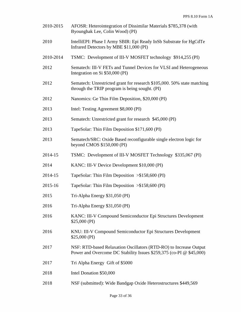
PPS 8.10 Form 1A
Page 33 of 36
2010-2015 AFOSR: Heterointegration of Dissimilar Materials $785,378 (with
Byounghak Lee, Colin Wood) (PI)
2010 IntelliEPI: Phase I Army SBIR: Epi Ready InSb Substrate for HgCdTe
Infrared Detectors by MBE $11,000 (PI)
2010-2014 TSMC: Development of III-V MOSFET technology $914,255 (PI)
2012 Sematech: III-V FETs and Tunnel Devices for VLSI and Heterogeneous
Integration on Si $50,000 (PI)
2012 Sematech: Unrestricted grant for research $105,000. 50% state matching
through the TRIP program is being sought. (PI)
2012 Nanomics: Ge Thin Film Deposition, $20,000 (PI)
2013 Intel: Testing Agreement $8,000 (PI)
2013 Sematech: Unrestricted grant for research $45,000 (PI)
2013 TapeSolar: Thin Film Deposition $171,600 (PI)
2013 Sematech/SRC: Oxide Based reconfigurable single electron logic for
beyond CMOS $150,000 (PI)
2014-15 TSMC: Development of III-V MOSFET Technology $335,067 (PI)
2014 KANC: III-V Device Development $10,000 (PI)
2014-15 TapeSolar: Thin Film Deposition >$158,600 (PI)
2015-16 TapeSolar: Thin Film Deposition >$158,600 (PI)
2015 Tri-Alpha Energy $31,050 (PI)
2016 Tri-Alpha Energy $31,050 (PI)
2016 KANC: III-V Compound Semiconductor Epi Structures Development
$25,000 (PI)
2016 KNU: III-V Compound Semiconductor Epi Structures Development
$25,000 (PI)
2017 NSF: RTD-based Relaxation Oscillators (RTD-RO) to Increase Output
Power and Overcome DC Stability Issues $259,375 (co-PI @ $45,000)
2017 Tri Alpha Energy Gift of $5000
2018 Intel Donation $50,000
2018 NSF (submitted): Wide Bandgap Oxide Heterostructures $449,569
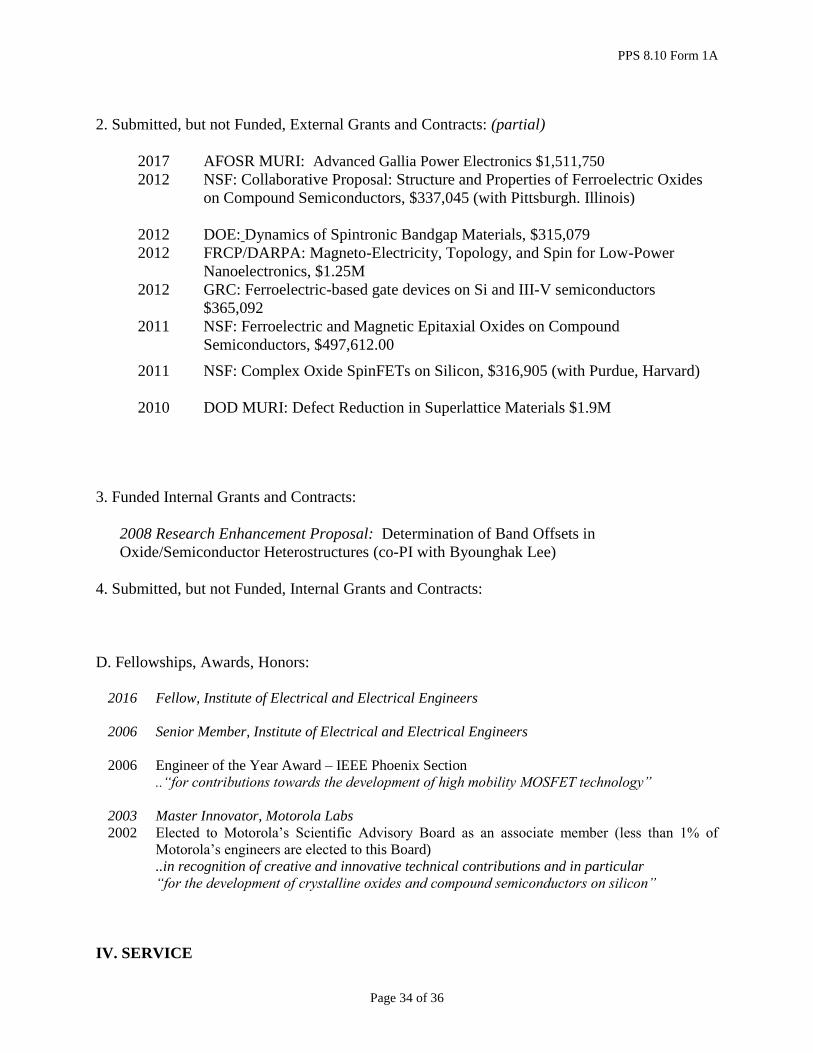
PPS 8.10 Form 1A
Page 34 of 36
2. Submitted, but not Funded, External Grants and Contracts: (partial)
2017 AFOSR MURI: Advanced Gallia Power Electronics $1,511,750
2012 NSF: Collaborative Proposal: Structure and Properties of Ferroelectric Oxides
on Compound Semiconductors, $337,045 (with Pittsburgh. Illinois)
2012 DOE: Dynamics of Spintronic Bandgap Materials, $315,079
2012 FRCP/DARPA: Magneto-Electricity, Topology, and Spin for Low-Power
Nanoelectronics, $1.25M
2012 GRC: Ferroelectric-based gate devices on Si and III-V semiconductors
$365,092
2011 NSF: Ferroelectric and Magnetic Epitaxial Oxides on Compound
Semiconductors, $497,612.00
2011 NSF: Complex Oxide SpinFETs on Silicon, $316,905 (with Purdue, Harvard)
2010 DOD MURI: Defect Reduction in Superlattice Materials $1.9M
3. Funded Internal Grants and Contracts:
2008 Research Enhancement Proposal: Determination of Band Offsets in
Oxide/Semiconductor Heterostructures (co-PI with Byounghak Lee)
4. Submitted, but not Funded, Internal Grants and Contracts:
D. Fellowships, Awards, Honors:
2016 Fellow, Institute of Electrical and Electrical Engineers
2006 Senior Member, Institute of Electrical and Electrical Engineers
2006 Engineer of the Year Award – IEEE Phoenix Section
..“for contributions towards the development of high mobility MOSFET technology”
2003 Master Innovator, Motorola Labs
2002 Elected to Motorola’s Scientific Advisory Board as an associate member (less than 1% of
Motorola’s engineers are elected to this Board)
..in recognition of creative and innovative technical contributions and in particular
“for the development of crystalline oxides and compound semiconductors on silicon”
IV. SERVICE

PPS 8.10 Form 1A
Page 35 of 36
A. University:
B. Departmental:
2008/9 Member search Committee: Asst/Assoc Professor (Engineering)
2009/10 Member search Committee: Asst/Assoc Professor (Physics)
2012 Chair, Dept. of Physics graduate degree program
2012 Chair, Dept. of Physics policy on annual evaluation
2011-13 Personnel Committee, Physics
2014 REP Committee Dept. Rep.
2015- Chair, Personnel Committee, Engineering
2016- MSEC Admissions Committee
C. Community:
D. Professional:
2009 Committee Member: 2009 North American MBE conference
2010 Committee Member: 2010 North American MBE conference
2011 Organizer and co-chair: 6th Multifunctional Materials Meeting, Alaska
2012 Organizer and co-chair: 7th Multifunctional Materials Meeting, Panama
2012 Session organizer and co-chair: International Symposium of Integrated
Functionalities, Hong Kong
2013 Session Chair: 40th Conference on the Physics and Chemistry of Surfaces and
Interfaces
2014 Co-chair, 9th Multifunctional Materials Meeting, India
2014 Organizing Committee, 18th International Conference on Molecular Beam
Epitaxy, AZ
2014 Session Chair, 18th International Conference on Molecular Beam Epitaxy, AZ
2015 Organizing Committee, North American Molecular Beam Epitaxy Conference,
Mexico
2016 Member, Program Committee, International Conference on Molecular Beam
Epitaxy
Reviewer for:
Journal of Crystal Growth
IEEE Electron Device Letters
Applied Physics Letters
National Science Foundation
Journal of Vacuum Science and Technology
E. Organizations
1. Honorary:
2. Professional:

PPS 8.10 Form 1A
Page 36 of 36
Fellow, Institute of Electrical and Electrical Engineers
Senior Member, Institute of Electrical and Electrical Engineers
Member, Materials Research Society
Member, American Vacuum Society
F. Services Honors and Awards: