i1 i2 - drum - university of maryland
TRANSCRIPT


ABSTRACT
Title of Dissertation: Novel Organic Polymeric and Molecular
Thin-Film Devices for Photonic Applications
Younggu Kim, Doctor of Philosophy, 2006
Dissertation directed by: Professor Chi H. Lee
Department of Electrical and
Computer Engineering
The primary objective of this thesis is to explore the functionalities of new classes
of novel organic materials and investigate their technological feasibilities for be-
coming novel photonic components.
First, we discuss the unique polarization properties of optical chiral waveguides.
Through a detailed experimental polarization analysis on planar waveguides, we
show that eigenmodes in planar chiral-core waveguides are indeed elliptically po-
larized and demonstrate waveguides having modes with polarization eccentricity
of 0.25, which agrees very well with recent theory. This is, to the best of our
knowledge, the first experimental demonstration of the mode ellipticities of the
chiral-core optical waveguides. In addition, we also examine organic magneto-optic

materials. Verdet constants are measured using balanced homodyne detection, and
we demonstrate organic materials with Verdet constants of 10.4 and 4.2 rad/T · m
at 1300 nm and 1550 nm, respectively.
Second, we present low-loss waveguides and microring resonators fabricated
from perfluorocyclobutyl copolymer. Design, fabrication and characterization of
these devices are addressed. We demonstrate straight waveguides with propagation
losses of 0.3 dB/cm and 1.1 dB/cm for a buried channel and pedestal structures,
respectively, and a microring resonator with a maximum extinction ratio of 4.87 dB,
quality factor Q = 8554, and finesse F = 55. In addition, from a microring-loaded
Mach-Zehnder interferometer, we demonstrate a modulation response width of
30 ps and a maximum modulation depth of 3.8 dB from an optical pump with a
pulse duration of 100 fs and a pulse energy of 500 pJ when the signal wavelength
is initially tuned close to one of the ring resonances.
Finally, we investigate a highly efficient organic bulk heterojunction photode-
tector fabricated from a blend of P3HT and C60. The effect of multilayer thin
film interference on the external quantum efficiency is discussed based on numer-
ical modeling. We experimentally demonstrate an external quantum efficiency
ηEQE = 87 ± 2% under an applied bias voltage V = −10 V, leading to an internal
quantum efficiency ηIQE ≈ 97%. These results show that the charge collection
efficiency across the intervening energy barriers can indeed reach near 100% under
a strong electric field.

Novel Organic Polymeric and Molecular Thin-Film Devices
for Photonic Applications
by
Younggu Kim
Dissertation submitted to the Faculty of the Graduate School of the
University of Maryland, College Park in partial fulfillment
of the requirements for the degree of
Doctor of Philosophy
2006
Advisory Committee:
Professor Chi H. Lee, Advisor/Chair
Doctor Warren N. Herman, Co-advisor
Professor Julius Goldhar
Professor Christopher C. Davis
Professor James R. Anderson

c© Copyright by
Younggu Kim
2006

DEDICATION
To the loving memory of my father,
and my mother
ii

ACKNOWLEDGMENTS
I am truly grateful for the advice, support, friendship, criticism, and collaboration
that I have received over the years during my graduate study at the University of
Maryland and my research on polymer photonics at the Laboratory for Physical
Sciences. LPS has been a really fascinating place to conduct research because of
the wonderful facilities and equipment as well as the many talented scientists and
engineers.
First of all, I am particularly indebted to Prof. Chi Lee for his advice through-
out my Ph.D research, and the tremendous amount of support and encouragement
when I would get stuck. His great enthusiasm for research and for playing ten-
nis impressed me often considering his age, and he sometimes reminded me of
my father who would be the same age as he. I am deeply grateful to Dr. Warren
Herman at the LPS who introduced me to this wonderful area of research on poly-
mer photonics and optoelectronics. He has been extremely patient in answering
my countless questions. Without a doubt, every single piece of knowledge on or-
ganic polymer optics I have acquired has benefited from daily interaction with him.
Along the way of my Ph.D study, I was lucky enough to have a second academic
advisor, Prof. Julius Goldhar. I am grateful for his fruitful insights and comments
on the experiments I have conducted. I will miss his sense of humor as well. I
iii

am also grateful to Prof. Chris Davis and Prof. Bob Anderson who agreed to serve
on my dissertation committee. When I was new to optics, I learned a lot through
classes I took from Prof. Davis. He was also generous enough to extend my final
exam when I had to go back to Korea for my father’s funeral.
I also would like to thank Prof. Victor Granastein who gave me a research
opportunity for the first year of my graduate study. He is a genuine gentleman
whom everybody loves. I deeply appreciate his support even after I left his group.
I have also benefited from many stimulating discussions with Prof. Tom Murphy on
a few numerical simulations. His Matlab codes were exceptionally helpful to design
ring resonator devices. In addition, his class on “Optical Communication Systems”
was definitely the best among the classes I took at the University of Maryland. I
also want to thank Dr. Danilo Romero, an expert on organic optoelectronic devices.
He not only fabricated a series of devices for my research but also patiently taught
me a lot on the physics of organic semiconductors.
All the thesis work described here would not have been possible without the
support and encouragement of my colleagues at the University of Maryland and
LPS: Toby Olver, Dan Hinkel, Steve Brown, Scott Horst, Lisa Lucas, Sal Mar-
tinez, Mike Khbeis, George de la Vergne, J.B. Dottellis, Russell Frizzell, Leslie
Lorenz, Mark Thornton, Greg Latini, Dr. Chris Richardson, Dr. Charles Krafft,
Prof. P. T. Ho, Dr. Rohit Grover, Dr. Vien Van, Dr. Kuldeep Amarnath, Victor
Yun, Dr. Yongzhang Leng, Dr. Paul Petruzzi, Dr. Wei-Lou Cao, Dr. Jungwhan Kim,
Min Du, and Yi-Hsing Peng, and more. Special thanks go to cleanroom manager
iv

Toby who has never turned down my request for help and made my work in the
cleanroom a lot easier, Dan who was truly helpful for device fabrication and SEM-
ing, Steve whom I bothered almost every day for stepper use, Dr. Cao who helped
me conduct various experiments, and Dr. Krafft who provided useful tips on the
experimental setup to measure the Faraday rotation.
Most of the work in my thesis has been done in strong collaboration with other
researchers outside of the University of Maryland and LPS. I would like to thank
Prof. Mark Green, Dr. Myungjin Lee and Dr. Henry Teng at N.Y. Polytechnic Uni-
versity, Prof. Andrzej Rajca at the University of Nebraska, Prof. Lin Pu at the
University of Virginia, Prof. Dennis Smith and Shengrong Chen at Clemson Uni-
versity, Prof. Seth Marder at Georgia Tech, Dr. Cheng Zhang at Norfolk University,
Dr. William Diffey at the U S Army, Dr. Andy Guenthner at NAWC China Lake.
I am grateful to Shuo-Yen Tseng, Glenn Hutchinson, Mike Bowen, Ricardo
Pizarro, Dyan Ali, Arthur Liu, and more, especially to Shuo-Yen and Glenn for
the time we spent together not only at LPS but also at Hard Times and Starbucks.
I will particularly miss the happy hour a lot. I also would like to thank several
fellow Korean friends in the department including Dong Hun Park, Soo Bum Lee,
Woochul Jeon, Jusub Kim, and Seokjin Kim for the occasional wonderful parties
and the time we spent on the tennis court, and Kyuyong Lee, Jeong-Nam Kim,
Kiyong Kim, Seungjoon Lee, Joonhyuk Yoo, Seung-Jong Baek, Kyechong Kim,
Sangchul Song, Inseok Choi, Hojin Kee, Jookyung Lee, and many more for their
friendship. My graduate study would not have been nearly as much fun without
v

them. Additionally, I want to thank Jeong-Il Oh who did not mind driving down
here from Boston when I was frustrated from work or life.
Most of all, I am deeply indebted to my family for their love, encouragement,
and support (including monetary support, as ‘indebted’ means in a dictionary)
over the years. No matter how many words I put here, it will never be sufficient to
express my true gratefulness to my dad in heaven, mom, parents-in-law, brother,
and sister. Finally, I would like to gratefully acknowledge Soyeon and Minju for
their constant love, sacrifice, and tolerance of my irregular hours at home.
vi

TABLE OF CONTENTS
Acknowledgments iii
List of Figures x
List of Abbreviations xviii
1 Introduction 1
1.1 Motivation . . . . . . . . . . . . . . . . . . . . . . . . . . . . . . . . 1
1.2 Scope of thesis . . . . . . . . . . . . . . . . . . . . . . . . . . . . . 3
2 Optical Chiral Waveguide 8
2.1 Organic chiral material and optical activity . . . . . . . . . . . . . . 8
2.2 Unique polarization properties of chiral-core planar waveguides . . . 11
2.2.1 Fields in bulk chiral media . . . . . . . . . . . . . . . . . . . 12
2.2.2 Eigenmodes in asymmetric chiral planar waveguides . . . . . 15
2.3 Chiral waveguides from amorphous binaphthyl films . . . . . . . . . 25
2.4 Experimental polarization analysis . . . . . . . . . . . . . . . . . . 34
2.5 Other chiral materials . . . . . . . . . . . . . . . . . . . . . . . . . 48
vii

2.5.1 Binaphthyl polymer . . . . . . . . . . . . . . . . . . . . . . . 49
2.5.2 Polymethine dyes . . . . . . . . . . . . . . . . . . . . . . . . 50
2.5.3 (7)Helicene . . . . . . . . . . . . . . . . . . . . . . . . . . . 52
2.5.4 Bridged binaphthyl with chromophore . . . . . . . . . . . . 52
2.6 Summary . . . . . . . . . . . . . . . . . . . . . . . . . . . . . . . . 53
3 Organic Magneto-Optic Material 55
3.1 Magneto-optic effect . . . . . . . . . . . . . . . . . . . . . . . . . . 55
3.2 Balanced homodyne detection . . . . . . . . . . . . . . . . . . . . . 58
3.3 Measurement of Verdet constant . . . . . . . . . . . . . . . . . . . . 63
3.4 Summary . . . . . . . . . . . . . . . . . . . . . . . . . . . . . . . . 72
4 Optical Waveguide and Microring Resonator from PFCB 74
4.1 Perfluorocyclobutyl (PFCB) copolymer . . . . . . . . . . . . . . . . 74
4.2 Low loss optical waveguide from PFCB copolymer . . . . . . . . . . 75
4.2.1 Eigenmodes in dielectric waveguides . . . . . . . . . . . . . 77
4.2.2 Fabrication of PFCB waveguides . . . . . . . . . . . . . . . 80
4.2.3 Loss measurement of straight waveguides . . . . . . . . . . . 84
4.3 PFCB Microring resonators . . . . . . . . . . . . . . . . . . . . . . 87
4.3.1 Basic principles . . . . . . . . . . . . . . . . . . . . . . . . . 88
4.3.2 Design considerations . . . . . . . . . . . . . . . . . . . . . . 94
4.3.3 Experimental characterization . . . . . . . . . . . . . . . . . 100
4.3.4 Ultrafast all-optical switching experiment . . . . . . . . . . . 106
viii

4.4 Summary . . . . . . . . . . . . . . . . . . . . . . . . . . . . . . . . 114
5 Organic Thin-Film Photodetector based on Bulk Heterojunction 117
5.1 Basic principles . . . . . . . . . . . . . . . . . . . . . . . . . . . . . 118
5.2 Fabrication of bulk heterojunction PDs . . . . . . . . . . . . . . . . 126
5.3 Device characteristics . . . . . . . . . . . . . . . . . . . . . . . . . . 131
5.4 Multilayer thin film interference effects . . . . . . . . . . . . . . . . 138
5.4.1 Optical properties of individual layers . . . . . . . . . . . . . 138
5.4.2 Effect of multilayer thin film interference . . . . . . . . . . . 140
5.5 Improvement of the external quantum efficiency . . . . . . . . . . . 152
5.6 Summary . . . . . . . . . . . . . . . . . . . . . . . . . . . . . . . . 156
6 Conclusions 158
6.1 Summary and accomplishments . . . . . . . . . . . . . . . . . . . . 158
6.2 Future work . . . . . . . . . . . . . . . . . . . . . . . . . . . . . . . 161
Bibliography 165
ix

LIST OF FIGURES
2.1 Structure of an asymmetric planar waveguide with an isotropic chi-
ral core . . . . . . . . . . . . . . . . . . . . . . . . . . . . . . . . . 16
2.2 Calculation of the mode effective index neff vs. waveguide thickness
d. . . . . . . . . . . . . . . . . . . . . . . . . . . . . . . . . . . . . 20
2.3 Calculation of the mode eccentricity parameter g vs. chirality γ for
the lowest order elliptical modes, RHE0 and LHE0. . . . . . . . . . 23
2.4 Chemical structure of the single molecule binaphthyls, ML-224 and
ML-226. . . . . . . . . . . . . . . . . . . . . . . . . . . . . . . . . . 26
2.5 Optical rotatory dispersion (ORD) curves for ML-224 and ML-226
measured in solution. . . . . . . . . . . . . . . . . . . . . . . . . . . 27
2.6 Index of refraction dispersion measured with a MetriconTM for ML-
224 and ML-226 . . . . . . . . . . . . . . . . . . . . . . . . . . . . 28
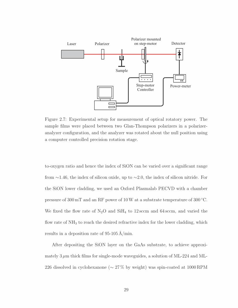
2.7 Experimental setup for measurement of optical rotatory power. . . 29
2.8 Structure of chiral slab waveguides on GaAs substrates coated with
SiON. . . . . . . . . . . . . . . . . . . . . . . . . . . . . . . . . . . 30
x

2.9 Calculation of neff with increasing waveguide core thickness, (a)
ML-224 and (b) ML-226. . . . . . . . . . . . . . . . . . . . . . . . 32
2.10 Calculation of mode ellipticity of RHE0 and LHE0 of the asymmet-
ric slab waveguide as a function of given material chirality γ. . . . 33
2.11 Experimental setup for polarization analysis for chiral waveguide. . 35
2.12 Detected optical power as a function of rotating quarter waveplate
orientation. . . . . . . . . . . . . . . . . . . . . . . . . . . . . . . . 38
2.13 Continuous evolution of the polarization states on the Poincare
sphere. . . . . . . . . . . . . . . . . . . . . . . . . . . . . . . . . . 40
2.14 Evolution of polarization through the chiral waveguide fabricated
from ML-224 and ML-226. . . . . . . . . . . . . . . . . . . . . . . . 44
2.15 Calculation of mode ellipticity of RHE0 and LHE0 as a function of
given material chirality γ for a symmetric and asymmetric chiral-
core planar waveguides. . . . . . . . . . . . . . . . . . . . . . . . . 47
2.16 Chemical structure of the main chain binaphthyl polymer, Zhang-
IV-37 with R = n-C6H13. . . . . . . . . . . . . . . . . . . . . . . . 49
2.17 Index of refraction dispersion measured with a MetriconTM for the
polybinaphthyl Zhang-IV-37 . . . . . . . . . . . . . . . . . . . . . . 50
2.18 UV-Vis-IR spectra measured with a Cary 5000 spectrophotometer
for HT-dye14 in poly(butyl methacrylate-co-methyl methacrylate)
copolymer. . . . . . . . . . . . . . . . . . . . . . . . . . . . . . . . 51
xi

3.1 Schematics of balanced homodyne detection. . . . . . . . . . . . . . 60
3.2 Normalized intensities along the principal axes I1, I2, and difference
I1 − I2 . . . . . . . . . . . . . . . . . . . . . . . . . . . . . . . . . . 60
3.3 Experimental setup of balanced homodyne detection to measure
the Verdet constant. . . . . . . . . . . . . . . . . . . . . . . . . . . 64
3.4 Calibration of the amplitude of alternating magnetic flux density
inside the Helmholtz coil. . . . . . . . . . . . . . . . . . . . . . . . 65
3.5 Optical bias curve without magnetic field applied for a 2 cm-long
rod of TGG sample obtained at wavelength 633 nm . . . . . . . . . 67
3.6 Faraday rotation measured from a 2 cm long rod of TGG at a wave-
length of 633 nm by varying magnetic field flux densities and a fit
to linear line. . . . . . . . . . . . . . . . . . . . . . . . . . . . . . . 68
3.7 Faraday rotation measured for a 2 cm-long rod of TGG at different
wavelengths . . . . . . . . . . . . . . . . . . . . . . . . . . . . . . . 68
3.8 Chemical structure of SJZ-87A . . . . . . . . . . . . . . . . . . . . 69
3.9 UV-Vis-IR transmission spectra measured with a Cary 5000 spec-
trophotometer for organic magneto-optic samples provided by Geor-
gia Tech. . . . . . . . . . . . . . . . . . . . . . . . . . . . . . . . . 70
3.10 Faraday rotation measured for the substrates only and for the sam-
ple labelled SJZ-87A at wavelengths of 1300 nm and 1550 nm. . . . 71
xii

3.11 Faraday rotation measured for the substrates only and for the sam-
ples labelled TK1V1292A320-A and TK1V1292A320-N at a wave-
length of 850 nm. . . . . . . . . . . . . . . . . . . . . . . . . . . . . 71
4.1 Thermal (a)polymerization and (b)copolymerization to PFCB-based
polymer from trifluorovinylaryl ether monomers . . . . . . . . . . . 76
4.2 Mode profile of the transverse electric field component |ex| for the
fundamental TE mode for a pedestal and buried channel . . . . . . 79
4.3 Outline of process steps to fabricate the PFCB waveguides. . . . . 82
4.4 Scanning electron micrograph of the PFCB pedestal waveguide. . 85
4.5 Loss measurement of PFCB straight waveguides using cutback method
for TE mode. . . . . . . . . . . . . . . . . . . . . . . . . . . . . . . 86
4.6 Schematic diagram of microring resonators. (a) all-pass and (b)
add-drop configuration. . . . . . . . . . . . . . . . . . . . . . . . . 88
4.7 Calculation of a typical spectral response of all-pass filter. . . . . . 91
4.8 Calculated phase response near a resonance in all-pass configuration 92
4.9 Calculation of a typical spectral response of add-drop filter . . . . . 93
4.10 3D full vectorial calculation for bending loss. . . . . . . . . . . . . 96
4.11 Cross-sectional mode profile of two parallel waveguides separated
by an edge-to-edge distance g. . . . . . . . . . . . . . . . . . . . . 98
4.12 Calculation of coupling constant between two PFCB pedestal waveg-
uides as a function of waveguide separation g. . . . . . . . . . . . 99
xiii

4.13 Scanning electron micrograph of PFCB ring resonator, with a ra-
dius R = 25 µm, and a coupling gap g = 0.45 µm. . . . . . . . . . 102
4.14 Experimental setup for microring characterization. . . . . . . . . . 103
4.15 Measured spectral response at the drop port of a add-drop filter
with a radius 25µm with ASE input . . . . . . . . . . . . . . . . . 104
4.16 Normalized signal of the device at the throughput and drop port
at the resonance at 1531.05 nm from a tunable laser input. . . . . 105
4.17 (a) Resonance shift with increasing ASE input power. Maximum
resonance shift 25 pm obtained. (b) Thermo-optic coefficient, dn/dT ,
measured using a MetriconTM that was custom outfitted with tem-
perature control. . . . . . . . . . . . . . . . . . . . . . . . . . . . 107
4.18 Schematic picture of all-optical switching experiment. . . . . . . . . 109
4.19 Spectral response of an MR-MZI with a length imbalance between
two arms of the MZI. . . . . . . . . . . . . . . . . . . . . . . . . . 111
4.20 Measured switching response of the MR-MZI from a optical pump,
a 100 fs Ti:Sapphire laser pulse . . . . . . . . . . . . . . . . . . . . 113
4.21 Calculated phase response near a resonance in all-pass configuration
when the ring is lossy and under-coupled . . . . . . . . . . . . . . . 115
5.1 Schematic drawing illustrating photoinduced charge transfer be-
tween a conjugated polymer (P3HT) and a fullerene (PCBM-C60). 119
xiv

5.2 (a) Schematic energy level diagram of electrodes, donor and accep-
tor material (b) Schematic illustration of photocurrent generation
in heterojunction PV cells and detectors. . . . . . . . . . . . . . . . 122
5.3 Schematic diagram depicting conceptually the photoinduced charge
transfer in (a)bilayer heterojunction and (b)bulk heterojunction . . 124
5.4 The chemical structure of the materials in bulk heterojunction layer
for organic photodetector . . . . . . . . . . . . . . . . . . . . . . . 127
5.5 Schematic diagram of the device configuration. . . . . . . . . . . . 128
5.6 Atomic force microscopy (AFM) images for four different PCBM-
C60 molar fractions x. . . . . . . . . . . . . . . . . . . . . . . . . . 130
5.7 Current density versus voltage (I-V ) characteristics of the bulk het-
erojunction device of MEH-PPV copolymer and PCBM-C60 with a
C60 molar fraction x = 0.57. . . . . . . . . . . . . . . . . . . . . . . 133
5.8 Absorption spectra of the blend of P3HT/PCBM-C60 . . . . . . . . 135
5.9 I-V characteristics of the bulk heterojunction device from P3HT
and PCBM-C60 with a C60/P3HT 1.1 in weight, (a) under AM 1.5
direct solar illumination (b) under different laser intensities at 532 nm.136
5.10 External quantum efficiency vs. bias voltage of the device of P3HT/PCBM-
C60 at wavelength of 532 nm . . . . . . . . . . . . . . . . . . . . . . 137
xv

5.11 (a) Real and imaginary index of refraction measured from the spec-
troscopic ellipsometric data and model fit with the Drude-Lorentz
model. (b) Comparison between the estimated transmission using
the n and k, and thickness from the best-fit model and the measured
transmission from a spectrophotometer. . . . . . . . . . . . . . . . 141
5.12 Optical properties of Al, PEDOT:PSS, and P3HT:C60 . . . . . . . 142
5.13 Schematic diagram of the multilayer device structure with the thick-
nesses and the optical electric fields in each layer, E+i and E−
i . . . . 143
5.14 Calculation of reflectivity RD and absorption AD = 1 − RD − TD
of the bulk heterojunction device of P3HT/C60 with a thickness of
100 nm. . . . . . . . . . . . . . . . . . . . . . . . . . . . . . . . . . 147
5.15 Calculation of field distribution |E(x)|2 as a function of position.
Modulus squared of the optical electric field |E(x)|2 is normalized
to the incident light field |E+0 |2. . . . . . . . . . . . . . . . . . . . . 148
5.16 Calculation of time-averaged absorbed power Q(x) as a function of
position. . . . . . . . . . . . . . . . . . . . . . . . . . . . . . . . . . 150
5.17 Calculation of field distribution |E(x)|2 and time-averaged absorbed
power Q(x) as a function of position for the device structure of
glass/ITO/P3HT:C60/Al. . . . . . . . . . . . . . . . . . . . . . . . 153
5.18 UV-Vis-IR transmission spectra for P3HT:C60 samples with three
different thicknesses. . . . . . . . . . . . . . . . . . . . . . . . . . . 154
xvi
5.19 Calculated upper limit of the external quantum efficiency ηLEQE as
a function of active layer thickness dA and the measured EQE at
bias V =-10 V, with and without PEDOT:PSS and LiF layers. . . . 155
5.20 Measured ηEQE as a function of applied reverse bias voltage (a) and
photocurrent at V = −10 V as a function of incident laser intensity
(b) for a device with a dA = 300 nm. . . . . . . . . . . . . . . . . . 157
xvii

LIST OF ABBREVIATIONS
TE Transverse electric
TM Transverse magnetic
RHC Right-handed circular
LHC Left-handed circular
RHE Right-handed elliptical
LHE Left-handed elliptical
SOP State of polarization
PECVD Plasma enhanced chemical vapor deposition
RIE Reactive ion etching
ICP-RIE Inductive coupled plasma RIE
SEM Scanning electron microscope
TGG Terbium gallium garnet
PFCB Perfluorocyclobutyl
BCB Bisbenzocyclobutene
CTE Coefficient of thermal expansion
FD Finite difference
PDL Polarization dependent loss
xviii

PML Perfectly matched layer
OCDF Optical channel dropping filter
OADF Optical add-drop filter
MZI Mach-Zehnder interferometer
MR-MZI Microring-loaded Mach-Zehnder interferometer
ASE Amplified spontaneous emission
EDFA Erbium doped fiber amplifier
FWHM Full width at half maximum
OPV Organic photovoltaic
OPD Organic photodetector
HOMO Highest occupied molecular orbital
LUMO Lowest unoccupied molecular orbital
OLED Organic light emitting diode
EQE External quantum efficiency
ICPE Incident photon to current conversion efficiency
IQE Internal quantum efficiency
PCE Power conversion efficiency
ITO Indium tin oxide
P3HT Poly(3-hexylthiophene-2,5-diyl)
PCBM-C60 [6,6]-phenyl-C61-butyric acid methyl ester
PEDOT Poly(3,4-ethylenedioxythiophene)
PSS Poly(styrenesulfonate)
xix

Chapter 1
Introduction
1.1 Motivation
Organic polymers and molecules have emerged as one of the most promising class of
materials for photonic and electronic applications due to their potential capabilities
and advantages such as moderate to high functionality, fabrication flexibility, sub-
strate compatibility, affordability, etc. While other material systems, such as inor-
ganic semiconductors (e.g., silicon, gallium arsenide, and indium phosphide, etc.),
glasses (e.g., silicon dioxide, silicon oxynitride, and silicon nitride, etc.), silicon
on insulator (SOI), lithium niobate, sol-gels, etc. have widely been used, organic
materials have become a new paradigm for various components in communication
systems, displays, sensors, solar cells, and so on. During the past decade, there has
been an explosive growth and development of both materials and devices. Repre-
sentative examples include waveguide based integrated-optic devices for essential
building blocks for optical communication systems based on linear/nonlinear op-
tical properties of the materials: interconnectors, polarization converters, filters,
switches, directional couplers, modulators, gratings [1, 2]. They also include opto-
electronic and electronic devices based on electroluminescent and (semi)conducting
1

properties of the materials: LEDs, photodetectors, photovoltaic cells, lasers, radio-
frequency identification (RFID) tags, field effect transistors (FETs) [3, 4].
Organic materials have great advantages in many aspects because of the abil-
ity to change the material properties synthetically by modifications in chemical
structure and composition. Advantages include:
• tunability of index of refraction (range of 1.3 – 2) and birefringence control
• low coupling loss from and to the fiber due to small Fresnel reflection and
mode mismatch
• low absorption loss at common telecommunication wavelength, 1310 nm and
1550 nm
• large class of 2nd and 3rd order nonlinear optical properties
• various optoelectronic properties such as photoluminescence, electrolumines-
cence, and (semi)conductivity
• easily formed into thin films via spin-coating, inkjet printing, dipping, etc.
• wide variety of substrate compatibility, such as glass, quartz, semiconductor,
printed circuit board, and even flexible ones
• fabrication flexibility – photolithography as well as non-conventional lithog-
raphy such as laser ablation, nano-imprinting, multi-photon absorption, etc.
2
• affordability – inexpensive materials, simple fabrication processes, and fast
turn-around time
On the other hand, organic devices have drawbacks in terms of environmental
performance and reliability, such as thermal aging and photo-oxidation. Many
research groups, including electrical engineers, chemists, and physicists, have been
making efforts to overcome such problems through further chemical modification
and extensive reliability testing, such that devices in some applications are already
in the market (OLED, for example) and some are soon to be commercially available.
New classes of organic materials for various applications are synthesized ev-
ery day. The primary objective of this thesis is to explore the functionalities
of those materials and investigate their technological feasibilities for constructing
novel photonic components.
1.2 Scope of thesis
This thesis is separated into three principal parts discussing different types of
devices that are somewhat independent of each other, but can be integrated into
single devices: chiral waveguides and magneto-optic materials, low-loss waveguides
and microring devices from perfluorinated polymer, and organic bulk heterojunc-
tion photodetectors.
Chapter 2 will discuss the unique polarization properties of optical chiral waveg-
uides that can be used for integrated-optic polarization converters or polarization
modulators provided that low loss amorphous films of sufficient chirality can be
3

fabricated. In an achiral film, as is well known, the modes are transverse electric
(TE) and transverse magnetic (TM). On the other hand, new modeling results for
(a)symmetric planar waveguides with chiral cores showed that the eigenmodes are
elliptically polarized modes, in general, with the polarization ellipticity depend-
ing on the chirality, which is related to the bulk rotatory power of material. For
an important design consideration, dependence of mode ellipticity on cladding in-
dex is also discussed, and we propose and demonstrate a SiON layer for a cladding
layer. Through a detailed experimental polarization analysis on asymmetric chiral-
core planar waveguides fabricated from binaphthyl-based organic single molecules,
the eigenmodes of chiral planar waveguides are characterized and their mode el-
lipticities are compared with the ones predicted in recent theory. We show that
eigenmodes in planar chiral-core waveguides are indeed two orthonormal elliptical
polarizations and demonstrate waveguides having modes with a polarization eccen-
tricity of 0.25, which agrees very well with the theory. Although the achieved mode
ellipticity is not large enough to meet the requirement – predominant circularly
polarized modes – for practical applications, this is, to the best of our knowledge,
the first experimental demonstration of the mode ellipticities for the transverse
electric field of the chiral-core optical waveguides. Characterizations and feasibil-
ities of several other chiral materials are also discussed. Unfortunately, none of
these materials exhibit both appreciable material chirality and negligible linear
birefringence at the same time. The design and synthesis of isotropic materials
with high chirality is in progress.
4

Chapter 3 will examine organic magneto-optic materials, which can be viable
alternatives to the chiral materials. In addition to polarization rotators, they also
can potentially be used for integrated-optic isolators or circulators. The Faraday
effect in magneto-optic materials in a magnetic field is another class of optical activ-
ity, and it is characterized by Verdet constant. Measuring the Verdet constants of
thin (10−100 µm) organic samples under a moderate magnetic field (< 100 Gauss)
can be very challenging. For this reason, we discuss balanced homodyne detection
that provides a highly sensitive technique to measure an angle of polarization ro-
tation as small as 0.5 × 10⁻⁶ rad. We demonstrate the Verdet constants of 10.4
and 4.2 rad/T · m at 1300 nm and 1550 nm, respectively, from an organic sample
provided by Georgia Tech, which is comparable to that of terbium gallium garnet.
This unique observation can lead to integrated-optic isolators or circulators from
a simple fabrication methodology including spin-casting and photolithography.
Chapter 4 will present low-loss waveguides and polymer microring resonators
fabricated from perfluorocyclobutyl (PFCB) copolymer. Among the many materi-
als for passive waveguide devices, fluorinated polymers are particularly attractive
because they have very low absorption loss at telecommunication wavelengths.
Low-loss waveguides are one of the most important building blocks in integrated-
optic communication systems because most passive and active devices consist of
simple straight and curved waveguide segments. For example, microring resonator
based devices have very simple configurations of straight waveguides and circular
rings, and the loss present in the ring is the most important parameter deter-
5

mining the device performance. For these reasons, this chapter is devoted to the
design, fabrication, and characterization of those devices using PFCB. We demon-
strate straight waveguides with propagation losses of 0.3 dB/cm and 1.1 dB/cm for
a buried channel and pedestal structures, respectively, and a microring resonator
with a maximum extinction ratio of 4.87 dB, quality factor Q = 8554, and finesse
F = 55. In addition, we demonstrate that all-optical switching with the PFCB
microring resonator is possible when it is optically pumped with a femtosecond
laser pulse of a sufficient energy. From a microring-loaded Mach-Zehnder inter-
ferometer, we demonstrate a modulation response width of 30 ps and a maximum
modulation depth of 3.8 dB from a optical pump with a pulse duration of 100 fs
and pulse energy of 500 pJ when the signal wavelength is initially tuned close to
one of the ring resonances.
Finally, chapter 5 will investigate a highly efficient organic bulk heterojunction
photodetector fabricated from a blend of conjugated polymer (P3HT) and small
molecule (fullerene C60). Although the organic thin film photodetector shares
fundamental photophysics with the organic photovoltaic cell in terms of the pho-
tocurrent generation process, the detector needs a slightly different approach from
that used in a photovoltaic cell. We address the effect of multilayer thin film in-
terference on the external quantum efficiency. From the numerical modelling to
calculate the optical field distribution and absorption in the layers, based on the
characterization of optical properties of individual layers comprising the detector,
we propose a bulk heterojunction photodetector without the PEDOT:PSS and LiF
6

layers that are commonly used in photovoltaic cells to achieve high short-circuit
current. Through the experimental I-V characterization, we demonstrate that it
exhibits an external quantum efficiency ηEQE = 87 ± 2% under an applied bias
voltage V = −10 V, leading to an internal quantum efficiency ηIQE ∼ 97%. These
results show that the charge collection efficiency across the intervening energy bar-
riers can indeed reach near 100% under a strong electric field.The achieved external
quantum efficiency is one of the highest values published so far.
7
Chapter 2
Optical Chiral Waveguide
2.1 Organic chiral material and optical activity
When molecules do not possess a plane of symmetry so that they are not superim-
posable on their mirror images through rotation and translation, they are referred
to as optical isomers or enantiomers and are said to be chiral. The word “chiral” is
derived from Greek meaning ‘hand’: our hands are mirror images and they cannot
be superimposed on each other no matter how hard we try.
Most of the physical and chemical properties of enantiomers are identical –
melting point, boiling point, density, solubility, etc. – but they can interact dif-
ferently in biological systems. For this reason, chiral molecules are of particular
interest in the pharmaceutical industry; of their two forms, one is clinically very
effective but the other is ineffective or even dangerous at times. One example
is thalidomide that was used for pregnant women in aiding morning sickness. It
was discovered, however, that one handedness of the molecule, (S )-thalidomide,
relieved the woman’s nausea, but the other handedness, R-enantiomer, caused hor-
rible birth defects. Another example of a chiral drug is ibupfofen, commonly found
in over-the-counter pain relievers. (R)-ibupfofen in racemic mixture is not only 100
8

times less effective, but also substantially slows the rate at which S -enantiomer
takes effect in the body [5,6].
When these chiral materials interact with electromagnetic waves, the plane of
polarization is rotated and they are said to be optically active. This optical activity
has been the subject of investigation for a few decades, especially in the microwave
and optics areas. Although quantum mechanics is required to give us a complete
understanding of the origin of the optical activity, it can simply be explained as
circular birefringence [7].
The modes in a chiral bulk material are right-handed circular polarization
(RHC) and left-handed circular polarization (LHC). When a linearly polarized
light enters into the chiral medium, it is decomposed into two orthogonal co-
propagating circular polarizations, RHC and LHC, travelling at different speeds
due to the circular birefringence. After propagating through the chiral material
and recombining, the output is linearly polarized as well, but is rotated by a certain
angle with respect to the plane of polarization of the incident wave. In general,
how much a certain chiral material rotates a plane of polarization is described
by specific rotatory power [α]25D in units of [ deg·cm2
dm·g], where 25 and D represents a
temperature of 25 C and a wavelength of the sodium D line at 589 nm, respectively.
The traditional sign convention for the optical activity in a chiral material is the
following: with light propagation through a sample towards an observer, α > 0
represents clockwise rotation and α < 0 represents counter-clockwise rotation when
viewed from the direction toward which the light is travelling (i.e. looking at the
9

light source). Sometimes, it is referred to as (+), right-handed or dextro-rotatory
chiral when α > 0, and (−), left-handed or levo-rotatory when α < 01. It should
be noted that this sign convention is exclusively used by chemists and the opposite
convention is adopted in many physics or engineering text books.
Organic chiral materials that form amorphous isotropic thin solid films have
potential use in optical waveguides for photonic applications. The recent theory [8]
on chiral-core planar waveguide suggests that an optical waveguide device may be
possible for novel applications, provided that low loss amorphous films of sufficient
chirality can be fabricated.
Useful applications include passive TE/TM mode converters for rotating the
output polarization of semiconductor lasers to optimize the polarization for down-
stream active waveguide devices in integrated optics, and active polarization con-
trol by combining an optically active waveguide segment with an electrooptic phase
shifter. There is a distinct advantage to achieving polarization rotation by optical
activity instead of linear birefringence. For a birefringent linear polarization rota-
tor, the input polarization must be at a 45 angle with respect to the optic axis
– a condition that is difficult to achieve in integrated optics. An optically active
bulk material that is isotropic, on the other hand, will rotate a linearly polarized
input of any orientation to a linearly polarized output.
To make use of this advantage in integrated optics, the eigenmodes of the chiral
1dextro and levo are from Latin meaning right and left, quite often they are used as d and l
in short, respectively.
10

waveguide must be circularly polarized. The challenge for this application is to
synthesize polymer or macromolecular structures with a high degree of chirality,
ultimately extending into the near infrared for telecommunication applications,
that also form amorphous isotropic thin films with negligible linear birefringence.
Large specific rotations on the order of 15,000 deg·cm2
dm·ghave been realized, for exam-
ple, with helicenes [9]. However, these molecules tend to aggregate in the formation
of thin films, a feature which can cause increased optical loss.
Although there has been relatively recent interest in the nonlinear optical prop-
erties of chiral materials, novel chiral photonic waveguides from linear chiral optical
effects are discussed here based on the development of chiral-core asymmetric slab
waveguides from amorphous organic binaphthyl films.
2.2 Unique polarization properties of chiral-core planar waveguides
Chirality in a dielectric planar waveguide introduces considerable mathematical
complexity, resulting in mode properties that can be significantly different from
those of the achiral case. This section reviews the theoretical analysis of the chiral
core planar (a)symmetric waveguides to provide a relatively comprehensive sum-
mary for later discussions. Although there are a number of theoretical papers
published, this section will mainly focus on reference [8] because all the analysis
performed in this chapter adopts the approach described there. It has the distinc-
tive advantage that the modal eigenvalue equations contain, in relatively simple
form, a pair of parameters determining the eccentricity of the polarization ellipse
11
for the transverse electric field.
2.2.1 Fields in bulk chiral media
When there are no “free” charges and currents inside the media (J = ρ = 0), the
electric and magnetic fields satisfy the Maxwell’s equations [10],
∇× E = −∂B
∂t, (2.1)
∇× H =∂D
∂t, (2.2)
∇ · D = 0, (2.3)
∇ · B = 0. (2.4)
The boundary conditions that must be satisfied by the electric and magnetic fields
at the interface between two different dielectric materials, designated 1 and 2, can
be expressed as
(E1 − E2) × n = 0, (2.5)
(H1 − H2) × n = 0, (2.6)
(D1 − D2) · n = 0, (2.7)
(H1 − H2) · n = 0. (2.8)
If we assume that all the field components have a time-dependence of ejωt,
E(r, t) = ReE(r) exp(jωt), (2.9)
H(r, t) = ReH(r) exp(jωt), (2.10)
12

we can rewrite the equations involving time derivatives, Eqs. 2.1 and 2.2, in terms
of complex field quantities.
∇× E = −jωB, (2.11)
∇× H = jωD. (2.12)
Next, we adopt the Drude-Born-Federov2 constitutive relation in order to introduce
material chirality from isotropic chiral media into Maxwell’s equations [13].
D = ǫ(E + γ∇× E), (2.13)
B = µ(H + γ∇× H), (2.14)
where ǫ and µ are the permittivity and permeability, and γ is the chirality having
the units of length. For reference, a chirality parameter γ of 1 pm corresponds to
a bulk rotatory power ρ of 15 deg/mm at a wavelength of 633 nm with an average
refractive index of 1.62. From Eq. 2.11–2.14, we can obtain
(1 − ω2µǫγ2)∇× E − ω2µǫγE + jωµH = 0, (2.15)
(1 − ω2µǫγ2)∇× H − ω2µǫγH − jωǫE = 0. (2.16)
These coupled equations can be reduced to Helmholtz wave equations with Bohren’s
decomposition of E and H,
F± ≡ E ± j
√
µ
ǫH, (2.17)
2Another choice for a constitutive relation describing isotropic chiral media may be the sym-
metrized Condon set, D = ǫE−jgωH and H = µH+jgωE. However, two constitutive equations,
Drude-Born-Federov and symmetrized Condon, are equivalent to first order in g and γ [11, 12].
13

or
E =1
2(F+ + F−), (2.18)
H =1
2j
√
ǫ
µ(F+ − F−). (2.19)
By using Eqs. 2.15 and 2.16, and from Eqs. 2.18 and 2.19, we can easily verify that
∇× F± = ∓k0n±F±, (2.20)
n± ≡ ng
1 ± δ, (2.21)
δ ≡ ω√
µǫγ = k0ngγ, (2.22)
where ng is the index of refraction,√
ǫ/ǫ0, since we assume µ = µ0, and k0 is the
free-space wave vector, 2π/λ0. Finally, we can obtain the Helmholtz equations for
F± by computing the curl of Eq. 2.20.
∇2F± + k20n
2±F± = 0. (2.23)
Note that, in bulk media, solutions of Eq. 2.20 have the form,
F± = (x ± jy)Foexp(−jk0n±z), (2.24)
representing plane waves with right-handed circular (RHC) and left-handed circu-
lar (LHC) polarization. In terms of handedness describing how the end point of
the electric field vector traces a circle or ellipse on a plane perpendicular to the
beam, there exist two opposing conventions. To avoid any confusion, we shall use
the convention throughout this chapter as used in most optics books: for the RHC
(LHC), the electric field vector rotates clockwise (counter-clockwise) in time at a
14

fixed position in space to an observer looking at the source of the light. In fact,
this convention seems more natural since the rotation of the electric field vector
and the direction of propagation form a right-handed screw (left-handed screw) in
space at a fixed time for the RHC (LHC) in our definition here. It is important to
note, however, that if e−jwt was used for a time dependence of field components
instead of e+jwt, the handedness would be reversed: F+ for LHC and F− for RHC.
Optical rotatory power due to the circular birefringence is given by
ρ =π
λo
(n− − n+) (2.25)
≃ k0ngδ, for δ ≪ 1, (2.26)
2.2.2 Eigenmodes in asymmetric chiral planar waveguides
As we discussed in section 2.2.1, the eigenmodes in bulk chiral media are RHC
and LHC polarizations. In a waveguide structure, however, the eigenmodes are
two orthonormal elliptically polarized modes in general – right-handed elliptical
(RHE) and left-handed elliptical (LHE) polarizations – due to influence of the
boundary conditions. This section describes in detail the polarization properties of
eigenmodes in an asymmetric chiral planar waveguide, using eigenvalue equations
in terms of a pair of parameters g and h corresponding to the ellipticity for the
transverse electric field [8]. Hence it allows a detailed insight into the polarization
properties.
Consider the planar waveguide structure shown in Fig. 2.1. The upper and
lower cladding layers are not chiral having indices of refraction no and ns, respec-
15

ng, g
x
y
0
-d
ns
no
Figure 2.1: The structure of an asymmetric planar waveguide with an isotropic
chiral core. The upper and lower cladding layers are not chiral having indices of
refraction no and ng, respectively, and the core layer has an index ng, chirality γ,
and thickness d. The coordinate axes have been oriented such that the waveguide
points in the z-direction and is assumed to be infinite in the ±x-direction.
16

tively, and the core layer has an index ng, chirality γ, and thickness d. The coor-
dinate axes have been oriented such that the waveguide points in the z-direction
and is assumed to be infinite in the ±x-direction. If we assume a solution for the
Helmholtz wave equation of the form,
F±(y, z) = Ψ±(y) exp(−jk0neffz), (2.27)
where neff is the effective index of a mode propagating along the +z-direction,
then the cartesian x-component of Ψ± satisfies the Helmholtz equation (putting
∂∂x
= 0):
dΨ±x (y)
dy2+ k2
0(n2q − n2
eff)Ψ±x = 0, (2.28)
where the subscript q in nq denotes the waveguide layer, ‘±’ in the core, ‘o’ in
the upper cladding, and ‘s’ in the lower cladding layer. As in the achiral slab
waveguide, the solution to the above equation can be written as
y =
A± exp(−vy) y ≥ 0
B± cos(u±y + φ±) 0 < y < −d
C± exp[w(y + d)] y ≤ −d
, (2.29)
where
u± ≡ k0
√
n2± − n2
eff ,
v ≡ k0
√
n2eff − n2
o, (2.30)
w ≡ k0
√
n2eff − n2
s.
17

The y and z-component of Ψ± can be obtained from Eq. 2.20 and Ψ±x (y),
Ψ±y (y) = ±j
neff
nq
Ψ±x (y), (2.31)
Ψ±z (y) = ± 1
k0nq
dΨ±x (y)
dy. (2.32)
From Eqs. 2.5 and 2.6 describing the boundary conditions that require continuity
of the tangential components of E and H across the interface at y = 0 and y = −d,
and using Eqs. 2.18–2.27, we can obtain a set of eight equations. Eliminating A±
from the four equations at y = 0, and C± from the remaining four equations at
y = −d yields
B+(σ+o sin φ+ − cos φ+) + B−(σ−
o sin φ− − cos φ−) = 0, (2.33)
B+(roσ+o sin φ+ − cos φ+) − B−(roσ
−o sin φ− − cos φ−) = 0, (2.34)
B+[σ+s sin (u+d − φ+) − cos (u+d − φ+)]
+ B−[σ−s sin (u−d − φ−) − cos (u−d − φ−)] = 0,
(2.35)
B+[rsσ+s sin (u+d − φ+) − cos (u+d − φ+)]
− B−[rsσ−s sin (u−d − φ−) − cos (u−d − φ−)] = 0,
(2.36)
where
σ±o ≡ (1 ± δ)
u±
v,
σ±s ≡ (1 ± δ)
u±
w, (2.37)
rp ≡n2
p
n2g
, p = o or s,
By introducing two equations – which equivalently satisfy the conditions that the
determinants of the coefficients B+ and B− in Eqs. 2.33 and 2.34, and Eqs. 2.35
18

and 2.36 are zeros – including new parameters g and h such that
cot φ± = σ±o
(
ro ± g
1 ± g
)
, (2.38)
cot (u±d − φ±) = σ±s
(
rs ± h
1 ± h
)
, (2.39)
and solving for the determinant, the four equations (Eqs. 2.33–2.36) can give a
single equation,
1 + h
1 − h=
S+ro
+ S+ro
g
S−ro
+ S−ro
g. (2.40)
Note that Eqs. 2.38, 2.39 and 2.40 represent five equations with five unknowns φ±,
g, h and neff , and equivalently state all the constraints imposed by the boundary
conditions. We can eliminate φ± in Eqs. 2.38 and 2.39, and solve Eq. 2.40 for h in
order to obtain eigenvalue equations along with the mode eccentricity parameters
g and h,
u±d = cot−1
(
σ±o
ro ± g
1 ± g
)
+ cot−1
(
σ±s
rs ± h
1 ± h
)
+ m±π, (2.41)
h(g, neff) =(S+
ro− S−
ro) + (S+
o − S−o )g
(S+ro
+ S−ro
) + (S+o − S−
o )g. (2.42)
It is worth noting that Eq. 2.41 has an inverse-trigonometric form, similar to the
achiral case that is familiar to us [14]. The two equations in Eq. 2.41 can be
simultaneously solved for g and neff with Eq. 2.42. For an example, Fig. 2.2 shows
the calculation for the mode effective index neff as a function of waveguide core
thickness d at a wavelength λ = 633 nm for the fundamental and the first higher
modes in an achiral (γ = 0) and a chiral (γ = 50 pm) asymmetric planar waveguide.
The refractive index of the core layer is ng = 1.62, and the upper and lower cladding
19

0 1 2 3 4 5 6 7 8 9 101.5
1.55
1.6
1.65
d (µm)
n eff
ng
TE0
TM0
TE1
TM1
(a) Achiral (γ = 0)
0 1 2 3 4 5 6 7 8 9 101.5
1.55
1.6
1.65
d (µm)
n eff
n+
n−
RHE0
LHE0
RHE1
LHE1
(b) Chiral (γ = 50pm)
Figure 2.2: Calculation of the mode effective index neff vs. waveguide thickness d,
for the fundamental and the first higher modes in (a) an achiral (γ = 0) and (b) a
chiral (γ = 50 pm) asymmetric planar waveguide. The refractive indices ng = 1.62,
no = 1.00, and ns = 1.50 are used for this calculation.
20

indices are no = 1.00 and ns = 1.50, respectively. The neff ’s for TE and TM in
the achiral case are asymptotic to the core index ng with increasing thickness far
from the cut-off. On the other hand, the neff ’s for RHE and LHE in the chiral
case are asymptotic to the core indices n+ and n−, respectively with increasing
thickness [8, 15,16].
Once g and neff are obtained, φ± can be found from Eq. 2.38, and other re-
maining constants for field amplitudes in Eq. 2.29 can be found as,
B+ = B− g + ro
g − ro
cos φ−
cos φ+, (2.43)
A± = B− cos φ− g ±√ro
g − ro
, (2.44)
C± = B− cos (u−d − φ−)h ±√
rs
h − rs
. (2.45)
From Eqs. 2.18 and 2.27, the transverse electric field is given by
ET =1
2
[
Ψ+y (y) − Ψ−
y (y)]
x + jneff
[
Ψ+y (y)
nq
−Ψ−
y (y)
nq
]
y
exp (−jk0neffz).
(2.46)
The polarization for the field given by the above equation is, in general, an elliptical
polarization with major axes on either the x or y axis. The mode eccentricity –
the ratio of the y-component to the x-component – in the upper cladding (y ≥ 0)
is given by
Ey
Ex
∣
∣
∣
∣
y≥0
= jneff
no
√ro
g= j
neff
ng
1
g, (2.47)
and the mode eccentricity in the lower cladding (y ≤ 0) is given by
Ey
Ex
∣
∣
∣
∣
y≤−d
= jneff
ns
√rs
h= j
neff
ng
1
h. (2.48)
21

The polarization ellipse in the core is more complicated than in the cladding and
varies with position in y, but considering the equation,
B+
B−=
g + 1
g − 1
√
√
√
√
√
√
1
σ+o
2 +(
g+ro
g+1
)2
1
σ−
o2 +
(
g−ro
g−1
)2 , (2.49)
gives an idea of the mode eccentricity. In limiting cases,
when γ → 0,
B− = B+, as g → ±∞ −→ TE
B− = −B+, as g → 0 −→ TM,
when γ 6= 0,
B+/B− → 1, as g → ±∞ −→ predominant TE
B+/B− → −1, as g → 0 −→ predominant TM
B+/B− ≫ 1, as g → 1 −→ predominant RHC
B+/B− ≪ 1, as g → −1 −→ predominant LHC.
Figure 2.3 illustrates the mode ellipticity parameter g as a function of chirality
γ for the fundamental elliptical modes, RHE0 and LHE0, in the asymmetric planar
waveguide with a 3µm thick chiral-core, an average core refractive index ng = 1.62,
and upper and lower cladding indices of no = 1.00 and ns = 1.50, respectively.
When γ > 0, the RHE(LHE) modes evolve from TM(TE) at γ = 0 and become
predominantly RHC(LHC) modes with increasing chirality.
22

−50 −40 −30 −20 −10 0 10 20 30 40 50
−1
1
γ (pm)
g
RHC
TM
LHC
RHE0
−50 −40 −30 −20 −10 0 10 20 30 40 50
−1
1
γ (pm)
1/g
RHC
TE
LHC
LHE0
Figure 2.3: Calculation of the mode eccentricity parameter g vs. chirality γ for the
lowest order elliptical modes, RHE0 and LHE0, in an asymmetric planar waveguide
with a 3 µm thick chiral-core, and refractive indices ng = 1.62, no = 1.00 and
ns = 1.50. When γ > 0, the RHE(LHE) modes evolve from TM(TE) at γ = 0 and
become predominantly RHC(LHC) modes with increasing chirality.
23

It should be noted that a small refractive index difference between the chiral-
core and the cladding can effectively enhance the chirality effect. In other words,
for a weakly guided waveguide structure, the mode ellipticity becomes close to
unity – more nearly circular – for a given material chirality γ.
One way to look at this quantitatively is by considering the asymptotic limit
of |σ±s | in Eq. 2.37,
|σ±s | =
∣
∣
∣
∣
∣
(1 ± δ)
√
n2± − n2
eff√
n2eff − n2
s
∣
∣
∣
∣
∣
(2.50)
≈√
2δ
1 − rs
, for neff → ng and δ ≪ 1, (2.51)
which is zero in the achiral case (δ = 0), and increases either with increasing δ
(proportional to the material chirality γ) or with increasing rs, related to the index
contrast ∆n as
∆n =ng − ns
ng
= 1 − 1√rs
. (2.52)
This can be explained qualitatively from the following: the mode in achiral
waveguides are TE and TM in general. However, the critical angle for total internal
reflection depends on the index difference between the core and cladding, therefore,
in the weakly confined waveguides, only light at a grazing incidence angle that
is bigger than the critical angle can be supported through the waveguide. This
confined mode in the achiral case can be considered as approximately TEM in
nature. Similarly, the RHE and LHE modes in chiral waveguides approximate as
RHC and LHC in bulk for the weakly confined waveguides.
It should be noted that the mode ellipticity changes dramatically in the vicinity
24

of mode crossover points – where the curve of neff for the RHE modes successively
cross over higher LHE modes, for example, neff for the RHE0 with LHE1 as in
Fig. 2.2(b). In fact, in addition to those eccentricity parameters g and h, this is one
of the most unique advantages using the theoretical developments in reference [8].
However, this does not concern us since we are primarily interested in a single
mode waveguide that supports only the fundamental modes RHE0 and LHE0.
2.3 Chiral waveguides from amorphous binaphthyl films
Planar waveguides fabricated from chiral single molecules, identified as ML-224 and
ML-226, synthesized by Prof. Green’s group at N. Y. Polytechnic University have
been investigated for detailed experimental polarization analysis. Fig. 2.4 shows
the chemical structures of both ML-224 and ML-226, which consist of binaphthyls
attached to cis-1,3,5-cyclohexanetricarboxylic ester. These binaphthyl based chi-
ral non-racemic compounds adopt a scheme designed to produce materials that
form glassy isotropic thin solid films with negligible linear birefringence [17]. The
bridged binaphthyls are based on work in [18], in which the thermal and photo-
racemization of these materials were used to explore fundamental characteristics of
the glassy state. The detailed synthetic work leading to ML-224 and ML-226 can
be found in [19]. The glass transition temperature Tg measured with a differential
scanning calorimeter (DSC) is in the range of 65−70 C and 45−50 C, and the spe-
cific rotatory power in solution measured with a polarimeter is [α]25D = +428 deg
and [α]25D = −468 deg, for ML-224 and ML-226, respectively. Note that ML-
25

X1
X2
O
O
X3
COOY
COOY
YOOC
Y =
Figure 2.4: Chemical structure of the single molecule binaphthyls attached to cis-
1,3,5-cyclohexanetricarboxylic ester. For ML-224, X1=H, X2=H and X3=CH2O-
heptyl, and for ML-226, X1=heptyl, X2=heptyl and X3=H.
224 is a right-handed (d -rotatory) chiral compound and ML-226 is a left-handed
(d -rotatory) chiral compound as shown in Fig. 2.5 for optical rotatory dispersion
(ORD) curves for both materials.
For thin solid films, the refractive index dispersion of these films was measured
using a MetriconTM prism coupler, which determines the ordinary and extraor-
dinary index of a film using two orthogonal linear polarizations at each of five
discrete laser wavelengths. Figure 2.6 shows the measured refractive indices of
the thin films fabricated from both ML-224 and ML-226, and curves fitted to the
Sellmeier dispersion relation,
n2 = A + Bλ2
λ2 − λ2o
, (2.53)
where λo is the wavelength corresponding to the absorption peak in the material.
As shown in the figure, both samples are isotropic within the experimental un-
certainty (∼ 0.0001). This isotropic property is extremely critical because even
moderate amounts of linear birefringence can overpower the effects of optical ac-
26

Wavelength (nm)
400 500 600 700 800
2000
1000
-1000
-2000
-3000
0
Sp
ec.
Ro
tatio
n
ML-224 (RH, d-rotatory)
ML-226 (LH, l-rotatory)
Figure 2.5: Optical rotatory dispersion (ORD) curves for ML-224 and ML-226.
ML-224 has a right-handed chirality and ML-226 has a left-handed chirality.
tivity.
The optical activity of the solid films was measured using a 670 nm laser with
the laser beam passing through the film at normal incidence. For these films,
normal incidence corresponds to propagation along the optic axis, and therefore
the circular birefringence can be measured independently of linear birefringence
effects. The sample films, which are several microns thick on a fused quartz sub-
strate, were placed between two Glan-Thompson polarizers in a polarizer-analyzer
configuration, and the analyzer was rotated about the null position using a com-
puter controlled precision rotation stage as depicted in Fig. 2.7. From a fit of the
data to a sine-squared curve, the change in the null position of the film on a UV-
grade fused quartz substrate was compared to the null for transmission through the
27

Inde
x o
f R
efra
ctio
n
Wavelength (nm)
Figure 2.6: Index of refraction dispersion measured with a MetriconTM prism cou-
pler for ML-224 and ML-226 in thin solid films. Both materials are isotropic within
the experimental uncertainty (∼ 0.0001).
substrate alone. Measured optical rotatory power at 670 nm is about 4−5 deg/mm
for both ML-224 and ML-226, which is consistent with the specific rotatory power
measured in solution.
Figure 2.8 depicts the structure of the asymmetric planar waveguide fabricated
from ML-224 and ML-226 for a detailed study of the polarization properties of
the eigenmodes. GaAs was used for a substrate simply due to its availability and
ease of cleaving, and SiON was selected for the lower cladding layer because its
refractive index can be easily tailored by controlling the ratio of the gas mixture in
plasma-enhanced chemical vapor deposition (PECVD). Theoretically, the nitrogen-
28
Laser DetectorPolarizer mounted on step-motorPolarizer
Sample
Power-meterStep-motor Controller
Figure 2.7: Experimental setup for measurement of optical rotatory power. The
sample films were placed between two Glan-Thompson polarizers in a polarizer-
analyzer configuration, and the analyzer was rotated about the null position using
a computer controlled precision rotation stage.
to-oxygen ratio and hence the index of SiON can be varied over a significant range
from ∼1.46, the index of silicon oxide, up to ∼2.0, the index of silicon nitride. For
the SiON lower cladding, we used an Oxford Plasmalab PECVD with a chamber
pressure of 300 mT and an RF power of 10 W at a substrate temperature of 300 C.
We fixed the flow rate of N2O and SiH4 to 12 sccm and 64 sccm, and varied the
flow rate of NH3 to reach the desired refractive index for the lower cladding, which
results in a deposition rate of 95-105 A/min.
After depositing the SiON layer on the GaAs substrate, to achieve approxi-
mately 3 µm thick films for single-mode waveguides, a solution of ML-224 and ML-
226 dissolved in cyclohexanone (∼ 27 % by weight) was spin-coated at 1000 RPM
29

GaAs (substrate)
SiON (lower cladding)
Chiral Core
Air (upper cladding)
Thickness, d ML-224 : 3.08 mm ML-226 : 2.85 mm
d
8 mm
Figure 2.8: Structure of chiral slab waveguides on GaAs substrates coated with
SiON.
ML-224 ML-226 SiON
Wavelength no ne no ne for ML-224 for ML-226
633 nm 1.6201 1.6200 1.6030 1.6030 1.6135 1.5945
Table 2.1: Refractive indices of chiral-core layers from ML-224 and ML-226, and
SiON lower cladding layers at 633 nm in the waveguide structure depicted in
Fig. 2.8.
30
for 30 s on SiON, and then cured in a Fisher Scientific vacuum convection oven
with N2 environment. The temperature was elevated from room temperature up to
Tg with a ramp rate of 3 C/min, soaked for 30 min, and naturally cooled down to
room temperature. For the final step, the waveguides were cleaved to form smooth
end facets for input and output coupling.
Two critical design points should be noted at this point. First, the waveguide
thickness was determined in order to satisfy single mode operation supporting the
first two orthogonal modes RHE0 and LHE0 only. Figure 2.9 shows the calculation
of mode effective index with increasing core thickness for each waveguide. The cut-
off thickness of the first higher order elliptical mode is 3.15 µm for the waveguide
from ML-224 and 2.8 µm for the waveguide from ML-226. Second, the refractive
index of the SiON lower cladding layer was adjusted to be close to that of the chiral-
core layer. As pointed out in section 2.2.2, a small index difference between the
chiral-core and the cladding layer, ng and ns, respectively, is desirable because it
can enhance the eccentricity of elliptical eigenmodes for a given amount of material
chirality. The index contrast, ∆n = (ng − ns)/ng at a wavelength of 633nm, was
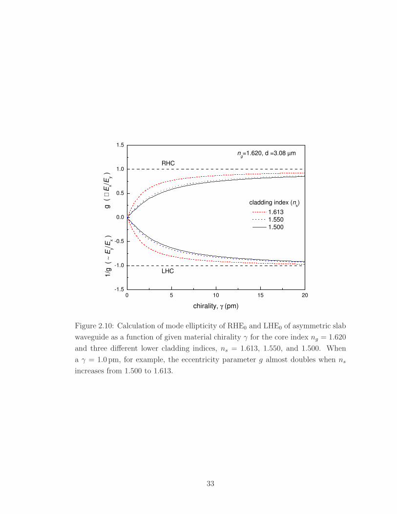
about 0.004-0.005 as shown in Tab. 2.1. Figure 2.10 shows the calculation of
ellipticity of the fundamental modes, RHE0 and LHE0 as a function of chirality γ
for three different lower cladding indices, 1.613, 1.550 and 1.500. When γ = 1.0 pm,
for example, the eccentricity parameter g almost doubles when ns increases from
1.500 to 1.613.
31

0 2 4 6 8 10
1.614
1.616
1.618
1.620
dc(LHE
1) = 3.15 µm
ML-224; ng=1.620, n
s=1.6135, γ =+0.3pm
mode e
ffective index, n
eff
waveguide thickness, d (µm)
LHE1
RHE1
RHE0
LHE0
0 2 4 6 8 10
1.596
1.598
1.600
1.602
dc(RHE
1) = 2.80 µm
ML-226; ng=1.603, n
s=1.5945, γ =-0.3pm
mode e
ffective index, n
eff
waveguide thickness, d (µm)
LHE1
RHE1
RHE0
LHE0
Figure 2.9: Calculation of neff with increasing waveguide core thickness. (a) The
cut-off thickness of LHE1 mode is about 3.15 µm for the waveguide from ML-224.
(b) The cut-off thickness of RHE1 mode is 2.8 µm for the waveguide from ML-226.
32
0 5 10 15 20-1.5
-1.0
-0.5
0.0
0.5
1.0
1.5
ng=1.620, d =3.08 µm
g (
∼ E
x/E
y )
cladding index (ns)
1.613
1.550
1.500
LHC
RHC
chirality, γ (pm)
1/g
(
∼ E
y/E
x )
Figure 2.10: Calculation of mode ellipticity of RHE0 and LHE0 of asymmetric slab
waveguide as a function of given material chirality γ for the core index ng = 1.620
and three different lower cladding indices, ns = 1.613, 1.550, and 1.500. When
a γ = 1.0 pm, for example, the eccentricity parameter g almost doubles when ns
increases from 1.500 to 1.613.
33

2.4 Experimental polarization analysis
In previous sections we discussed the theoretical polarization properties of the
eigenmodes and fabrication of asymmetric planar chiral-core waveguide from bi-
naphthyl based chiral compounds including key design parameters. For experi-
mental polarization analysis of these thin film waveguides, the state of polarization
(SOP) represented by normalized Stokes parameters of the eigenmodes was charac-
terized by determining the SOP at the output of the waveguide for two orthogonal
input polarizations: horizontal and vertical polarizations. We refer to these or-
thogonal linearly polarized inputs as TE and TM with respect to the slab surface
because, in an achiral slab waveguide, they would excite usual TE and TM modes.
For chiral waveguides, a linearly polarized input will excite both eigenmodes, RHE
and LHE, and the TE input excites a different relative fraction of these elliptical
eigenmodes than the TM input. As the light propagates down the waveguide, the
RHE and LHE modes travel at different speeds resulting in an overall elliptical
polarization with a rotated major axis at the output of the waveguide. If the
eigenmodes are circular, the output polarization is a linear polarization as well
but rotated by a certain angle. By determining the output polarization state for
a given input state, the eigenmodes of the slab waveguide can be computed.
As illustrated in Fig. 2.11 for the experimental setup, we used an intensity
stabilized He-Ne laser for a light source and a Faraday isolator after the laser
to prevent any undesired back-reflection into the laser cavity from deteriorating
34

Intensity-stabilized He-Ne Laser
Faraday
Isolator
Polarization Controller
Objective
LensCleaved Fiber
Single-mode Fiber
Collimator
Aperture
Power-meter
Step-motor Controller
Detector
Polarizer
Rotatingλ/4 plate
Figure 2.11: Experimental setup for polarization analysis for chiral waveguide.
the laser stabilization. Light is then directed through a polarization controller to
launch a specific polarization into the waveguide under measurement. An objective
lens was used for input coupling and a cleaved single mode fiber was used for
output coupling, both mounted on a 3-axis translation stage, allowing accurate
and stable alignment. The light signal travels through the additional single mode
fiber after the waveguide, and it is collimated and detected after passing through a
polarization analyzer section consisting of a rotating quarter waveplate and a linear
polarizer. The quarter waveplate is mounted on a rotating step motor controlled
by a computer.
The polarization analyzer section in Fig. 2.11 can be described using Stokes
35
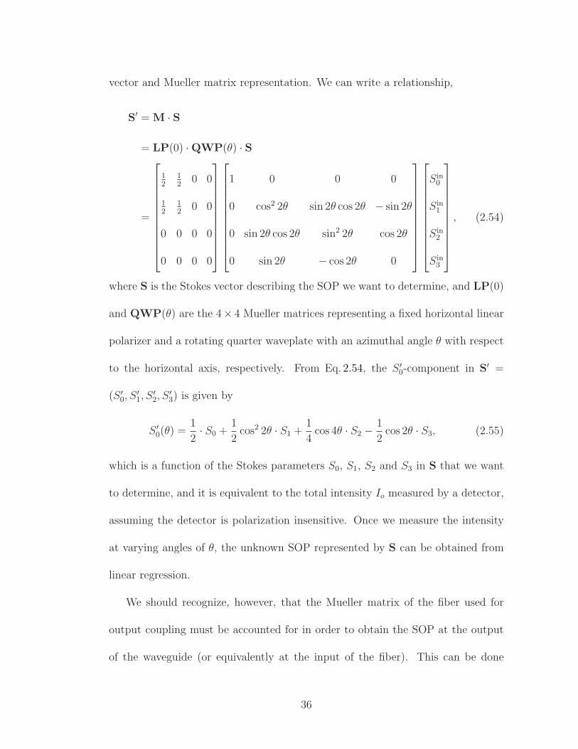
vector and Mueller matrix representation. We can write a relationship,
S′ = M · S
= LP(0) · QWP(θ) · S
=
12
12
0 0
12
12
0 0
0 0 0 0
0 0 0 0
1 0 0 0
0 cos2 2θ sin 2θ cos 2θ − sin 2θ
0 sin 2θ cos 2θ sin2 2θ cos 2θ
0 sin 2θ − cos 2θ 0
Sin0
Sin1
Sin2
Sin3
, (2.54)
where S is the Stokes vector describing the SOP we want to determine, and LP(0)
and QWP(θ) are the 4× 4 Mueller matrices representing a fixed horizontal linear
polarizer and a rotating quarter waveplate with an azimuthal angle θ with respect
to the horizontal axis, respectively. From Eq. 2.54, the S ′0-component in S′ =
(S ′0, S
′1, S
′2, S
′3) is given by
S ′0(θ) =
1
2· S0 +
1
2cos2 2θ · S1 +
1
4cos 4θ · S2 −
1
2cos 2θ · S3, (2.55)
which is a function of the Stokes parameters S0, S1, S2 and S3 in S that we want
to determine, and it is equivalent to the total intensity Io measured by a detector,
assuming the detector is polarization insensitive. Once we measure the intensity
at varying angles of θ, the unknown SOP represented by S can be obtained from
linear regression.
We should recognize, however, that the Mueller matrix of the fiber used for
output coupling must be accounted for in order to obtain the SOP at the output
of the waveguide (or equivalently at the input of the fiber). This can be done
36

by a calibration process in which three different input polarizations, [s1, s2, s3]3 =
[1 0 0], [0 1 0] and [0 0 1] representing horizontal linear polarization, 45 linear
polarization and RHC polarization, respectively, are launched into the fiber and
the resulting output SOP for each case is determined from the linear regression as
above [20]. This calibration procedure finds a characteristic 3× 3 Mueller matrix4
Mfiber [21] that determines the SOP at the output of the fiber for a given input
state. The matrix Mfiber can then be inverted to determine the SOP at the input
of the fiber (and thus the output of the chiral waveguide) when the SOP at the
output of the fiber is known.
Figure 2.12 shows the measurement results to determine the Stokes parame-
ters corresponding to the polarization states of the waveguide modes after the
additional single mode fiber. The dots represent the detected optical power as a
function of θ, the angle of the fast axis of a rotating quarter waveplate with respect
to the transmission axis of a fixed linear polarizer for two input polarizations sI of
TE and TM. As discussed above, from linear curve fitting and after taking into
account Mfiber, we obtained polarization states at the waveguide output sF
3[s1, s2, s3] is a normalized Stokes vector obtained by dividing the 4-Stokes vector by the total
optical power S0, i.e., s1 = S1/S0, s2 = S2/S0, s3 = S3/S0.
4When we ignore the loss in the fiber, it can be considered as a unitary optical system and
represented by the 3 × 3 Mueller matrix, a subset of a 4 × 4 Mueller matrix in which the first
row and the first column is always [1000] and [1000]T for the unitary optical component.
Mfiber =
m11 m12 m13
m21 m22 m23
m31 m32 m33
37

0 50 100 150 200 250 300 3500
0.2
0.4
0.6
0.8
1
Angle (Deg)
Nor
mal
ized
Inte
nsity
TE input, measuredTE input, fittedTM input, measuredTM input, fitted
(a) ML-224
0 50 100 150 200 250 300 3500
0.2
0.4
0.6
0.8
1
Angle (Deg)
Nor
mal
ized
Inte
nsity
TE input, measuredTE input, fittedTM input, measuredTM input, fitted
(b) ML-226
Figure 2.12: Detected optical power as a function of the angle between the rotating
quarter waveplate and polarizer to determine the Stokes parameters corresponding
to the polarization states of the waveguide modes. The solid lines fit to Eq. 2.55
for slab waveguides fabricated from (a) ML-224 and (b) ML-226.
38

for ML-224 waveguide
sFTE input =
0.75
−0.42
0.50
, sFTM input =
−0.72
0.45
−0.51
, (2.56)
and for ML-226 waveguide
sFTE input =
0.55
−0.06
−0.81
, sFTM input =
−0.53
0.08
−0.82
. (2.57)
Next, we want to obtain the Stokes parameters describing the eigenstates of the
waveguide from the SOP at the waveguide output for a given input polarization.
The continuous evolution of the polarization states through the waveguide can be
described by
dS
dz= Ω × S, (2.58)
where Ω is the waveguide eigenmode with projections Ω1, Ω2, and Ω3 defined in
the same coordinate space as the Stokes vector S. The above equation states that
while the light signal propagates down the waveguide from any initial position,
the evolution of the polarization state continuously traces out a circular orbit
perpendicular to an axis connecting orthogonal eigenstates on the Poincare sphere.
The evolution from the initial state sI to the final state sF can be easily visualized
on the Poincare sphere as illustrated in Fig. 2.13 [22]. For example, when the
eigenstates are circularly polarized modes, in other words, when the vector Ω is
39

Ω
SISF
S1
S3
S2
(a) Circularly polarized eigenstates
Ω
SI
SF
S1
S3
S2
Θ
(b) Elliptically polarized eigenstates
Figure 2.13: Continuous evolution of polarization states traces out a circular orbit
perpendicular to an axis connecting orthogonal eigenstates on the Poincare sphere.
(a) For circularly polarized eigenstates, the initial TE input polarization moves
along the equator and remains a linear polarization rotating continuously. (b) For
elliptically polarized eigenstates, the initial TE input polarization evolves into an
elliptical polarization in general.
40

directed along the S3 axis as shown in Fig. 2.4(a), the initial TE (s = [1 0 0]) input
polarization moves along the equator and remains a linear polarization rotating
continuously. If the initial polarization state is represented by a point either at
the north pole (RHC, sI = [0 0 1]) or at the south pole (LHC, sI = [0 0 − 1]),
the SOP does not change. On the other hand, when eigenstates are elliptically
polarized modes as shown in Fig. 2.4(b), the initial TE input polarization becomes
an elliptical polarization in general. As discussed in section 2.2.2, the eigenmodes
for a chiral planar waveguide are elliptical polarizations in general with major axes
on either the x or y axis, which correspond to the points on the S1 − S3 meridian
plane. So the eigenvector Ω can be written as
Ω =
sin Φ
0
cos Φ
, (2.59)
where Φ is the angle between the S3 axis and Ω as depicted in Fig. 2.13. In terms
of two angles Φ and Θ, the relationship between sI and sF can be written as
sF = Rs2(−Φ) · Rs3(Θ) · Rs2(Φ) · sI (2.60)
where RS2and RS3
are the matrices for rotational vector transformation with
41

respect to the S2 and S3 axis, respectively, and they are given by
RS2(Φ) =
cos Φ 0 − sin Φ
1 1 0
sin Φ 0 cos Φ
, (2.61)
RS3(Θ) =
cos Θ sin Θ 0
− sin Θ cos Θ 0
0 0 1
. (2.62)
For the TE input polarization (sI=[1 0 0]), after some algebraic manipulation with
trigonometric identities, we get
sF1 = 1 − 2 cos2 Φ sin2 Θ
2,
sF2 = 2 cos Φ sin
Θ
2cos
Θ
2, (2.63)
sF3 = 2 cos Φ sin Φ sin2 Θ
2,
and we can compute the angles ΦTE and ΘTE,
ΦTE = tan−1
(
sF3
1 − sF1
)
, (2.64)
ΘTE = 2 tan−1
(
sF3
sF2 sin ΦTE
)
. (2.65)
Similarly for the TM input polarization (sI=[−1 0 0]),
ΦTM = tan−1
( −sF3
1 + sF1
)
, (2.66)
ΘTM = 2 tan−1
(
sF3
sF2 sin ΦTM
.
)
(2.67)
42

For ML-224 waveguide
ΩTE input = ±
0.88
0
0.47
, ΩTM input = ±
−0.90
0
−0.44
, (2.68)
and for the ML-226 waveguide,
ΩTE input = ±
0.88
0
−0.48
, ΩTM input = ±
−0.88
0
0.47
, (2.69)
Since s3 for the polarization ellipse with major axes on either the x or y axis
is given by
s3 =2ExEy
E2x + E2
y
, (2.70)
it can be related to the ellipticity g when neff ≈ ng as in
s3 ≈2g
1 + g2for neff ≈ ng. (2.71)
From the above relation, the ellipticity parameter g is approximately 0.25 for the
waveguides from both ML-224 and ML-226. Figure 2.14 illustrates the evolution
of the SOP through the chiral waveguides fabricated from ML-224 and ML-226.
In order to look at the quantitative property of how the SOP evolves along the
waveguide as a function of the propagation distance z and the difference in mode
effective indices nLHE0
eff − nRHE0
eff , we can multiply a scale factor k0(nLHE0
eff − nRHE0
eff )
to the Ω in Eq. 2.58. However, often an alternative approach using the Jones
representation can be more intuitive and useful. From two orthonormal Jones
43
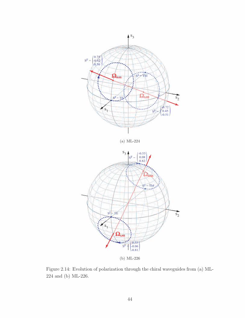
S3
S2
S1
SI = TE
0.75
-0.42
0.50(SF = )
-0.72
0.45
-0.51(SF = )
ΩRHE
(a) ML-224
S3
S2
S1
SI = TE
ΩLHE
0.55
-0.06
-0.81(SF = )
-0.53
0.08
0.82(SF = )
(b) ML-226
Figure 2.14: Evolution of polarization through the chiral waveguides from (a) ML-
224 and (b) ML-226.
44

vectors for the basis vectors corresponding to elliptical polarization states, which
are given by
E = Err + Ell, (2.72)
r =1√
a2 + b2
a
jb
, (2.73)
l =1√
a2 + b2
b
−ja
, (2.74)
r† · r = l† · l = 1, r† · l = l† · r = 0, (2.75)
we can construct a unitary transformation matrix representing a change of basis
states from Cartesian to elliptical
U =1√
a2 + b2
a −jb
b ja
, (2.76)
satisfying
Er
El
= U
Ex
Ey
, (2.77)
Now for the Jones vector after propagating a distance d through the chiral
waveguide with linear basis, we can write
E ′x
E ′y
z=d
= U† · Mwg · U ·
Ex
Ey
z=0
, (2.78)
where
Mwg =
e−jk0nrd 0
0 e−jk0nld
. (2.79)
45

If we put [Ex Ey] = [1 0], nr = nRHE0
eff , and nl = nLHE0
eff into Eq. 2.78, we can
achieve the polarization state [E ′x E ′
y] at z = d evolved from TE input at z = 0.
Note that the angle Θ in Fig. 2.4 is related to the propagation distance z and
∆neff = nLHE0
eff − nRHE0
eff such that
Θ = 2ρeffz, (2.80)
ρeff =π
λ(nLHE0
eff − nRHE0
eff ). (2.81)
Therefore, ρeffz = π corresponds to one complete circle around the eigenstate Ω.
The measured waveguide lengths d are about 16.5 mm and 11.7 mm, and from the
numerical calculations as shown in Fig. 2.9, the mode effective index differences are
approximately neff = 5 × 10⁻⁵ and ∆neff = −8 × 10⁻⁵ for the ML-224 and ML-
226 waveguides, respectively. Once these values are plugged into Eq. 2.80, we can
notice that, for both waveguides, the polarization states evolve in such a way that
they reach sF as given in Eqs. 2.56 and 2.57 after making one full complete circle.
The experimental results show that the eigenmodes of the chiral waveguides are
indeed RHE and LHE, and they are in excellent agreement with what is expected
from the theory in [8] in terms of the mode ellipticity and the SOP evolution
through the chiral-core planar waveguides.
Nevertheless, these Ω3 values are not large enough for these materials to be
used for a polarization controller or a TE/TM converter. We discussed that the
Ω3 of the eigenmode must be very close to unity, corresponding to predominantly
right- and left-handed circularly polarized waveguide modes. This can be achieved
46

0 5 10 15 20-1.5
-1.0
-0.5
0.0
0.5
1.0
1.5
ng=1.620, d =3.08 µm
1.613/1.62/1.613, Symmetric
LHC
chirality, γ (pm)
g (
∼ E
x/E
y )
1/g
(
∼ E
y/E
x )
RHC
1/1.62/1.613, Asymmetric
Figure 2.15: Calculation of mode ellipticity of RHE0 and LHE0 as a function of
given material chirality γ for the symmetric and asymmetric chiral-core planar
waveguides. The dotted line is associated with an asymmetric structure with
refractive indices ng = 1.62, n0 = 1.00 and ns = 1.613, and the solid line with a
symmetric structure with indices ng = 1.62 and n0 = ns = 1.613.
principally from larger specific rotatory power (or equivalently larger chirality γ)
of the material itself.
Figure 2.15 shows a calculation of the mode ellipticity of RHE0 and LHE0 as
a function of given material chirality γ for the symmetric and asymmetric chiral-
core planar waveguides. The dotted line is associated with an asymmetric structure
with refractive indices ng = 1.62, n0 = 1.00 and ns = 1.613, and the solid line with
a symmetric structure with indices ng = 1.62 and n0 = ns = 1.613. From the plot,
47

it is evident that, in order to have predominantly circular eigen-polarizations, a
chirality γ > 20 pm, or equivalently ρ > 300 deg/mm is required in the asymmetric
waveguide. On the other hand, in the symmetric waveguide, near circularly polar-
ized eigenstates can be obtained with considerably a lower chirality γ ≈ 4− 5 pm,
or equivalently ρ = 45 − 60 deg/mm.
The desire for circularly polarized modes, rather than just elliptically polarized
modes, is driven by the goal of achieving a pure polarization rotator in a waveguide,
i.e. a device for which a linearly polarized input is rotated to some other linearly
polarized state for any propagation length. Because even moderate amounts of
linear birefringence can overpower the effects of optical activity, an essential re-
quirement that must be fulfilled in order to attain this goal is the synthesis of a
chiral material that is isotropic in a solid film.
2.5 Other chiral materials
Other than the chiral single molecules, ML-224 and ML-226, we have charac-
terized several organic chiral materials from strong collaborations with university
chemists: Prof. Mark Green’s group at New York Polytechnic University, Prof. An-
drzej Rajca’s group at the University of Nebraska, and Prof. Lin Pu’s group at the
University of Virginia. Although the improvement in material chirality was modest
so that they were not realized into actual devices, here we summarize the charac-
teristics of those materials including optical rotatory power and index dispersion
measured using the same method described in section 2.4.
48

O O
OR
RO
O O
OR
RO
Figure 2.16: Chemical structure of the main chain binaphthyl polymer, Zhang-IV-
37 with R = n-C6H13.
2.5.1 Binaphthyl polymer
A main chain binaphthyl polymer identified as Zhang-IV-37 shown in Fig. 2.16
was supplied by the University of Virginia. The glass transition temperature Tg is
expected to be in the range of 200 C and the specific rotatory power measured in
solution is [α]25D = −711 .
For characterization, a 0.95 µm thick sample was prepared on a UV-grade fused
quartz by dissolving the solid powder in cyclohexanone to make a 10 % solution
and spin-casting followed by curing in an oven at 100 C for two hours. The optical
rotatory power measured is −8.7 deg/mm at 670 nm, which is almost twice as big
as ML-224 and ML-226. However, it exhibited a marked linear birefringence of
49

400 600 800 1000 1200 1400 16001.60
1.62
1.64
1.66
1.68
1.70
Index o
f re
fraction
Wavelength (nm)
no
ne
Figure 2.17: Index of refraction dispersion measured with a MetriconTM prism
coupler for the polybinaphthyl Zhang-IV-37 in thin solid films, which exhibited a
marked large linear birefringence, ∼ −0.01.
∼ −0.01 as shown in Fig. 2.17.
From Eq. 2.21 with Eq. 2.22, we can notice that this appreciably large linear
birefringence is almost 300 times bigger than the circular birefringence, and hence
the eigenstates of the planar waveguide would be approximately TE/TM modes.
2.5.2 Polymethine dyes
A chiral polymethine dye identified as HT-dye14 was supplied by NY Polytechnic
University and its polymer composite with a poly(butyl methacrylate-co-methyl
methacrylate) was characterized. The glass transition temperature Tg for HT-
dye14 and poly(butyl methacrylate-co-methyl methacylate) are about 122 C and
50

200 400 600 800 1000 1200 1400 1600 1800 20000
2
4
6
8
Abs. coeffic
ient (µ
m-1)
Wavelength (nm)
HT-dye14 100%
HT-dye14 22%
HT-dye14 3%
Figure 2.18: UV-Vis-IR spectra measured with a Cary 5000 spectrophotometer for
HT-dye14 in poly(butyl methacrylate-co-methyl methacrylate) copolymer.
64 C, respectively. Due to the π−π∗ absorption of the chromophore in polymethine
dyes, there is a strong absorption in the 550–700 nm spectral range. Figure 2.18
shows UV-Vis-IR spectra for the absorption coefficient measured with a Cary 5000
spectrophotometer for three samples with different concentrations of HT-dye14 in
the copolymer.
Both materials were dissolved separately in chloroform and mixed afterwards.
After casting the film, it was cured at a temperature of 170 C, substantially
above the Tg, for an hour because annealing can be quite effective in removing
51

birefringence arising from strain in the evaporation process [23]. Optical rotatory
power measured at 751 nm was about -3 deg/mm for the sample consisting of 22 %
dye in the copolymer, and -72 deg/mm for the sample from pure HT-dye14 without
the copolymer. The linear birefringence of pure HT-dye14 is 0.004−0.01 depending
upon wavelength. As we decrease the concentration of polymethine dye molecules,
the material composite becomes isotropic. For example, the sample consisting
of 22 % dye was isotropic within experimental uncertainty, ∼ 0.0001, but with a
trade-off in optical activity, -3 deg/mm.
2.5.3 (7)Helicene
Thiophene-based carbon-sulfur (7)helicene chiral molecular glass was supplied by
the University of Nebraska [24]. Tg is about 67 C and the specific rotatory power
measured in solution is [α]25D = +1166 . A 5.6 µm thick sample was made by drop-
dispensing from the solution in cyclohexanone. The optical rotatory powers were
11 deg/mm and 6 deg/mm at wavelengths of 670 nm and 850 nm, respectively, and
the linear birefringence was ∼ 0.0003.
2.5.4 Bridged binaphthyl with chromophore
Bridged binaphthyls with chromophore groups attached, identified as HT-386, was
supplied by NY Polytechnic University. A 2 µm thick sample was prepared by
spin-casting the solution in cyclohexanone. The optical rotatory power measured
was about 11 deg/mm at 670 nm. The refractive index measurement shows the
sample is isotropic within the experimental uncertainty (∼ 0.0001). However, Tg
52

is around 25 C, so it was difficult to fabricate waveguide structures.
2.6 Summary
In this chapter, we discussed the unique polarization properties of optical chiral
waveguides that can be used for integrated-optic polarization converters or polar-
ization modulators provided that low loss amorphous films of sufficient chirality
can be fabricated. Relatively recently, new modeling results for (a)symmetric
planar waveguides with chiral cores showed that eigenmodes are elliptically po-
larized modes, in general, and the polarization ellipticity depends on the chirality
that is related to the bulk rotatory power of material. For an important design
consideration, dependence of mode ellipticity on cladding index was discussed.
Through a detailed experimental polarization analysis on asymmetric chiral-core
planar waveguides fabricated from binaphthyl-based organic single molecules with
a layer of SiON for the cladding layer, we showed that eigenmodes in planar chiral-
core waveguides are indeed two orthonormal elliptical polarizations, and achieved
waveguide modes with a polarization eccentricity of 0.25, which agrees very well
with the theory. Although the achieved mode ellipticity is not large enough to
meet the requirement – predominant circularly polarized modes – for practical
applications, this is, to the best of our knowledge, the first experimental demon-
stration of the mode ellipticities for the transverse electric field of the chiral-core
optical waveguides. As we discussed, even in the case of weekly confined sym-
metric waveguide structure, the chirality γ > 5pm is required for near circularly
53

polarized eigenmodes. Characterizations and feasibilities of several other chiral
materials were also discussed. Unfortunately, none of these materials exhibited
both the appreciable material chirality and negligible linear birefringence at the
same time. The design and synthesis of such an isotropic material with a high
degree of chirality, which also extends the ORD maxima into the near infrared, is
in progress.
54

Chapter 3
Organic Magneto-Optic Material
3.1 Magneto-optic effect
The magneto-optic effect refers to a phenomenon in which light propagating through
a medium experiences birefringence in the presence of a magnetic field. There
are two well-known magneto-optic effects, distinguished by the direction of the
magnetic field with respect to the direction of light propagation, Faraday and
Cotton-Mouton. The Cotton-Mouton effect arises from a linear birefringence pro-
portional to the square of the transverse magnetic field flux density. The magnetic
field-induced linear birefringence ∆n can be written as
∆n = n‖ − n⊥
= CCMλB2t , (3.1)
where n‖ and n⊥ are the refractive indices for light polarized parallel and perpen-
dicular to the magnetic field, respectively, CCM is the Cotton-Mouton coefficient,
and Bt is the transverse component of the magnetic field. Therefore, the phase
55

difference ∆φCM between the two orthogonal polarizations is given by
∆φCM =2π
λ∆nl
= 2πCCMB2t l, (3.2)
where l is the effective optical path length through a medium.
On the other hand, the Faraday effect comes from a circular birefringence
linearly proportional to the axial component of the magnetic field. Between these
two, the Faraday effect is well studied because of its practical importance for
useful optical components, such as isolators, circulators, polarization modulators,
and sensors including current sensors and magnetic field sensors.
The Faraday effect, the magnetic field-induced optical activity, was discovered
in 1845 by M. Faraday. The plane of polarized light can be rotated by allowing
light to propagate through a medium with inversion symmetry in the presence of
a magnetic field. The angle of rotation is given by
φF = V
∫
B · dl, (3.3)
where B is the magnetic flux density, dl is an infinitesimal displacement vector
along the direction of propagation of light, and V is a proportional constant called
Verdet constant. In words, the amount of polarization rotation is proportional to
the strength of the longitudinal component of the magnetic field and the length of
the medium the light propagates through.
The Verdet constant is associated with the specific material and in general
varies with wavelength and temperature [25–27]. The units of V are often ex-
56

pressed in [rad/T · m] or [min/G · cm]. By convention, a positive Verdet constant
corresponds to a counter-clockwise rotation when light propagates parallel to an
applied B-field and viewed from the direction toward which light is travelling (i.e.
looking at the light source) [28,29]. In other words, for V > 0, the plane of polar-
ization rotates in the same direction as the current through a solenoid coil around
the medium, regardless of the direction of light propagation. Note that this con-
vention for the sense of rotation is opposite from the optical activity in a chiral
medium, in which α > 0 represents a clockwise rotation when looking at the light
source as discussed in the previous chapter.
From the consideration of the reciprocity nature in optics, there is an important
difference between the Faraday effect and optical chiral activity. In the Faraday
effect, the rotation of polarization is non-reciprocal because the interaction of light
with matter under a magnetic field breaks the time reversal symmetry and the
parity conservation [30]. A detailed theoretical discussion on the origin of the
magneto-optic effect from a quantum mechanical approach is beyond the scope of
this thesis and will be omitted.
Most recently, a very high Verdet constant from an organic polymer thin film
has been reported [31]. Although there is a lack of theoretical understanding on the
physics of the high Verdet constants in organic polymers at this point, such kinds of
materials are essential to constructing integrated-optic devices such as isolators and
circulators from simple fabrication method of spin-casting and photolithography.
57

3.2 Balanced homodyne detection
To measure the Verdet constant associated with a particular material, we can
simply increase an effective path length or use a strong magnetic field to produce
a rotation angle large enough until it becomes detectable. However, in order to
detect a small angle of rotation from a thin organic film with a typical thickness of
10 − 100 µm in a moderate magnetic field < 100 Gauss, a measurement technique
with high precision and improved signal-to-noise ratio is essential. One of the
simplest ways to measure the Faraday rotation is based on the polarizer-analyzer
configuration that we used to measure the optical rotatory power of a chiral thin
film, but it suffers from poor measurement sensitivity and accuracy, on the order of
a few mdeg. The method relies highly on the accuracy and repeatability of a step
motor used in the measurement. A few other schemes for sensitive measurement
have been reported [32, 33]. However, the sensitivity is generally worse than a
balanced homodyne detection that we adopted in our experiment [34,35].
In optical interferometry, in order to detect a phase or amplitude change in an
optical signal, the signal and reference are mixed for phase comparison. When the
reference frequency ωLO from a local oscillator is slightly different from the signal
frequency ωS, the average current detected arises from an optical field at the differ-
ence frequency ωLO − ωS (often referred to as the intermediate frequency, IF), but
no other frequencies such as 2ωLO or 2ωS are detected simply because semiconduc-
tor detectors do not respond rapidly enough. The advantage of this Heterodyne
58

detection is that one can increase the S/N ratio by increasing the local oscillator
power and achieve shot-noise limit detection in which shot noise dominates over
all other noise contributions. On the other hand, when the frequency of the local
oscillator is same as that of the signal (ωLO = ωS), but there is a relative phase
difference, it is called Homodyne detection. In homodyne detection, the phase dif-
ference is transformed into an intensity change after an optical mixer, therefore the
total intensity at the photodetector is determined by the relative phase difference
between the signal and the local oscillator [36,37].
In a balanced homodyne interferometry scheme designed to measure the Verdet
constant with a high sensitivity and S/N ratio, a linearly polarized light oriented at
45 can be used as a probe beam instead of using two separate beams. Therefore,
the two orthogonal principal polarizations – horizontal and vertical – can be treated
as the two separate beams for the signal and the reference. Once the plane of
polarization is rotated by a small angle after propagating through the magneto-
optic sample placed in a magnetic field, the small amplitude changes are projected
onto the corresponding principal components of a polarizing beam splitter as shown
in Fig. 3.1.
In addition, if a sample is placed in an AC magnetic field, the rotation of polar-
ization from an alternating magnetic flux density is transformed into an amplitude
modulation along the principal axis after passing through the polarizing beam
splitter. Because the amplitude changes along the principal axes are 180 out of
phase from each other, by using a balanced photodetector consisting of two pho-
59
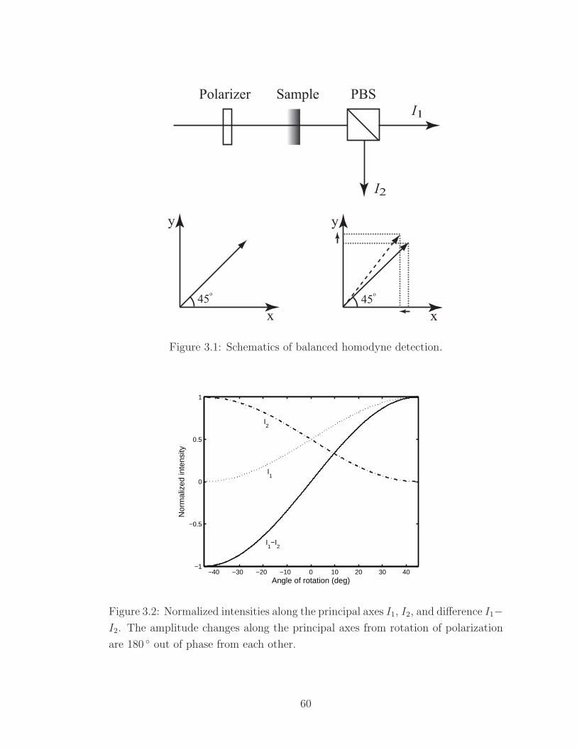
Polarizer Sample PBS
I1
I2
x
y
45o
x
y
45o
Figure 3.1: Schematics of balanced homodyne detection.
−40 −30 −20 −10 0 10 20 30 40−1
−0.5
0
0.5
1
Angle of rotation (deg)
Nor
mal
ized
inte
nsity
I1
I2
I1−I
2
Figure 3.2: Normalized intensities along the principal axes I1, I2, and difference I1−I2. The amplitude changes along the principal axes from rotation of polarization
are 180 out of phase from each other.
60

todiodes and a differential amplifier, and a lock-in amplifier, we can minimize the
amplitude noise of the optical field and maximize the sensitivity with a significant
rejection of common-mode noise.
We can use the Jones formalism for a quantitative analysis of the balanced
homodyne detection. The electric field E1 and E2 at each detector can be written
as
E1,2x
E1,2y
= Pol(θ1,2p ) · HWP(θh) · Rot(φ) · 1√
2
1
1
, (3.4)
where Pol(θ1,2p ), HWP(θh), and Rot(φ) represent the Jones matrices for the po-
larizing beam splitter, the half-wave plate with the fast-axis oriented at θh, and
the rotation by an angle of φ, respectively, which are given as
Pol(θ1,2p ) =
cos2 θ1,2p sin θ1,2
p cos θ1,2p
cos θ1,2p sin θ1,2
p sin2 θ1,2p
, (3.5)
HWP(θh) =
j cos2 θh − j sin2 θh j sin 2θh
j sin 2θh j sin2 θh − j cos2 θh
, (3.6)
Rot(φ) =
cos φ − sin φ
sin φ cos φ
. (3.7)
Because the polarizing beam splitter is aligned in such a way that θ1p = 0 and
θ2p = π/2, and each detector measures the intensity of the corresponding principal
component (horizontal and vertical polarization), the electric fields E1 and E2 at
61

each detector from Eq. 3.4 can be written as
E1x
E1y
=1√2
sin (2θh − φ) + cos (2θh − φ)
0
, (3.8)
E2x
E2y
=1√2
sin (2θh − φ) − cos (2θh − φ)
0
, (3.9)
and the output from the balanced detector can be represented as
I ∝ I1 − I2
∝ E†1 · E1 − E
†2 · E2 (3.10)
∝ sin 2(2θh − φ) + constant (3.11)
= A sin 2(2θh − φ) + C. (3.12)
When an alternating magnetic field is applied, the modulated intensity at a
fixed bias point θh = θh0 is given by
∆I = −2A cos 2(2θh0 − φ)∆φ, (3.13)
∆φ = V lB0 sin ωt, (3.14)
φF = V lB0. (3.15)
Eq. 3.12 can be referred to as an optical bias curve or a transfer curve, which can
be obtained from measuring the output from the balanced detector while rotating
the half-wave plate without a magnetic field applied. Note that obtaining the
optical bias curve is a necessary step for the absolute measurement of a rotation
angle from the corresponding amplitude modulation. In other words, once we
62

obtain the A and C in the optical bias curve from curve fitting, we can convert
the demodulated signal ∆I from the lock-in amplifier into the equivalent rotation
angle of plane polarization.
Also note that the bias point θh0 can be any arbitrary value for measuring
the Faraday rotation, but the maximum demodulated signal |∆I| from the lock-in
amplifier can be achieved at 2θh0 = φ. This is the case of 45 input polarization
and horizontal alignment of the fast axis of the half-wave plate. Even when there
is a misalignment of the input polarizer or inherent linear birefringence in the
sample, the bias point for maximum demodulation can be found from the optical
bias curve.
3.3 Measurement of Verdet constant
In this section, we discuss the experimental measurement of the Verdet constant
in detail and present the measurement result for terbium gallium garnet (TGG),
one of the most popular Faraday materials used for free space optical isolators,
and for the organic samples.
Figure 3.3 depicts the experimental setup we used to measure the Verdet con-
stant. A Glan-Thompson polarizer with an extinction ratio better than 50 dB was
used to produce a linearly polarized input oriented at 45 . The sample was placed
in a Helmholtz coil through which a sinusoidal current was applied from a power
supply controlled by a function generator. We used a KEPCO BOP70-12 power
supply to amplify the voltage signal from a function generator to provide suffi-
63

Laser
Balanceddetector
Polarizer
Sample
Function generator
Helmholtz coil
Lock-in
Power supply
Wollastonprism
λ/2
Step-motor
Controller
Figure 3.3: Experimental setup of balanced homodyne detection to measure the
Verdet constant. The rotation of polarization through the sample placed in an
alternating magnetic field is transformed into an amplitude modulation along the
principal axis after passing through the Wollaston prism, and detected by a bal-
anced detector.
64

0 2 4 6 8 10 120
50
100
150
200
250
Vpp (V)
Mag
netic
Fie
ld (
G)
10 Hz
50 Hz
100 Hz
200 Hz
Figure 3.4: Calibration of the amplitude of alternating magnetic flux density inside
the Helmholtz coil for a given input AC voltage signal to power supply. Due to
the inductive impedance, the magnetic field decreases with increasing frequency.
cient current through the Helmholtz coil. After light passes through the Wollaston
prism, the rotation of polarization from an alternating magnetic flux density is
transformed into an amplitude modulation along the principal axis (horizontal and
vertical), and detected by a New Focus balanced detector and a Signal Recovery
lock-in amplifier.
As a first step, an alternating magnetic field flux density B0 sin ωt inside the
Helmholtz coil for a given AC signal was calibrated using a gauss-meter from T.W.
Bell. Figure 3.4 shows the amplitude of the AC magnetic field B0 measured with an
increasing peak-to-peak voltage amplitude at different frequencies from a function
65

generator. Due to the inductive impedance of the circuit√
R2 + ω2L2, the current
flowing through the Helmholtz coil and hence the magnetic field decreases with
increasing frequency. Because 1/f noise dominates over other noise sources at a
low frequency detection, a modulation frequency of 100 Hz was chosen to reduce
1/f noise and produce a reasonably strong magnetic field at the same time. This
choice was somewhat arbitrary, but we experimentally verified that the Faraday
rotation measured with different modulation frequencies were indeed the same
although it can affect the S/N ratio.
For a verification of our experimental procedure, we measured a 2 cm-long rod of
TGG at wavelengths of 633 nm, 850 nm, 1300 nm, and 1550 nm. As we discussed
in the previous section, the optical bias curve without applying magnetic field
was obtained by measuring the output from the balanced detector while rotating
the half-wave plate mounted on a computer-controlled step motor and fitting to
Eq. 3.12 as shown in Fig. 3.5.
From the optical bias curve obtained, the demodulated signal from the lock-in
amplifier representing the RMS value of amplitude modulation can be converted
to an angle of rotation for a given applied magnetic field. Note that the demodu-
lated signal for different magnetic flux density is averaged over one hundred data
points. As shown in Fig 3.6, we can determine the Verdet constant by fitting the
angles of rotation at different magnetic field values to a linear line, as indicated
in Eqs. 3.13-3.15. The measured Verdet constant of TGG is -141 rad/T · m at a
wavelength of 633 nm, which agrees well with a published value [25]. Note that
66
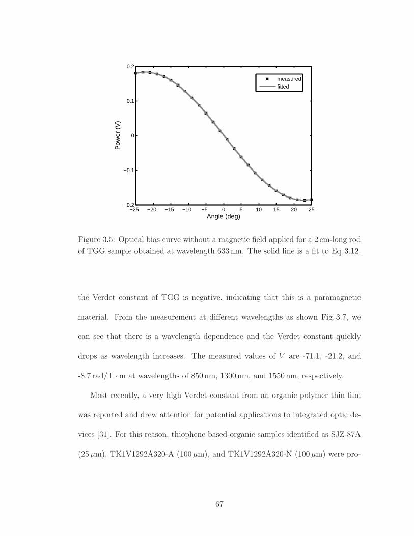
−25 −20 −15 −10 −5 0 5 10 15 20 25−0.2
−0.1
0
0.1
0.2
Angle (deg)
Pow
er (
V)
measuredfitted
Figure 3.5: Optical bias curve without a magnetic field applied for a 2 cm-long rod
of TGG sample obtained at wavelength 633 nm. The solid line is a fit to Eq. 3.12.
the Verdet constant of TGG is negative, indicating that this is a paramagnetic
material. From the measurement at different wavelengths as shown Fig. 3.7, we
can see that there is a wavelength dependence and the Verdet constant quickly
drops as wavelength increases. The measured values of V are -71.1, -21.2, and
-8.7 rad/T · m at wavelengths of 850 nm, 1300 nm, and 1550 nm, respectively.
Most recently, a very high Verdet constant from an organic polymer thin film
was reported and drew attention for potential applications to integrated optic de-
vices [31]. For this reason, thiophene based-organic samples identified as SJZ-87A
(25 µm), TK1V1292A320-A (100µm), and TK1V1292A320-N (100µm) were pro-
67

0 20 40 60 80 1000
0.01
0.02
0.03
Magnetic Field (Gauss)
Rot
atio
n (r
ad)
measuredfitted
Figure 3.6: Faraday rotation measured from a 2 cm long rod of TGG at a wave-
length of 633 nm by varying magnetic field flux densities and a fit to linear line.
0 20 40 60 80 1000
0.002
0.004
0.006
0.008
0.01
Magnetic Field (Gauss)
Rot
atio
n (r
ad)
633 nm 850 nm
1300 nm
1550 nm
Figure 3.7: Faraday rotation measured for a 2 cm-long rod of TGG at different
wavelengths
68

Figure 3.8: Chemical structure of SJZ-87A
vided by Prof. Seth Marder’s group at Georgia Tech. All three of them were drop-
dispensed and sandwiched by two glass substrates with a spacer. Figure 3.9 shows
the UV-Vis-IR transmission spectra of the samples measured with a Cary 5000
spectrophotometer.
We measured the Verdet constant of SJZ-87A at wavelengths of 1300 nm and
1550 nm, and the Verdet constants of TK1V1292A320-A and TK1V1292A320-N at
850 nm. Note that the substrate has a small but finite Verdet constant that must
be isolated. Hence, by measuring an angle of rotation from the substrate only,
the net rotation from the organic samples were determined. The measured Verdet
constant of the substrate was 2.9, 1.3, and 0.9 rad/T · m at 850 nm, 1300 nm, and
1550 nm, respectively. The values of V for SJZ-87A were 10.4 and 4.2 rad/T · m at
1300 nm and 1550 nm, respectively. For TK1V1292A320-A and TK1V1292A320-N,
the values were -4.7 and -4.2 rad/T · m at 850 nm, respectively.
The measured Verdet constants of these organic samples are about a half or
less than that of TGG, but new chemical structures based on polythiopene are
under development. To date, constructing integrated-optic isolators or circulators
69
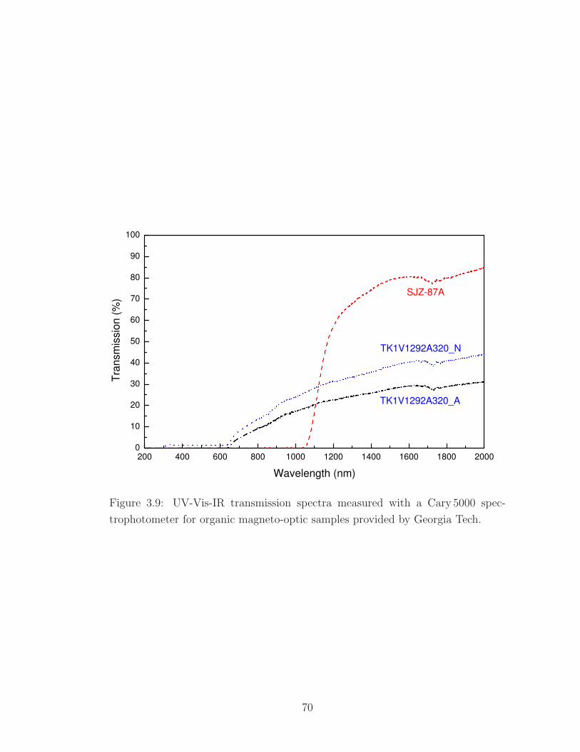
200 400 600 800 1000 1200 1400 1600 1800 20000
10
20
30
40
50
60
70
80
90
100
TK1V1292A320_A
TK1V1292A320_N
Tra
nsm
issio
n (
%)
Wavelength (nm)
SJZ-87A
Figure 3.9: UV-Vis-IR transmission spectra measured with a Cary 5000 spec-
trophotometer for organic magneto-optic samples provided by Georgia Tech.
70

0 20 40 60 80 100 1200
0.5
1
1.5
2
2.5
3
3.5
4x 10
−5
Magnetic Field (Gauss)
Rot
atio
n (r
ad)
substrate at 1300nm
substrate at 1550nm
SJZ−87A at 1300nm
SJZ−87A at 1550nm
Figure 3.10: Faraday rotation measured for the substrates only and for the sample
labelled SJZ-87A at wavelengths of 1300 nm and 1550 nm.
0 20 40 60 80 100 1200
1
2
3
4
5
6
7
8x 10
−5
Magnetic Field (Gauss)
Rot
atio
n (r
ad)
substrate measuredsubstrate fittedTK1V1292A320−A measuredTK1V1292A320−A fittedTK1V1292A320−N measuredTK1V1292A320−N fitted
Figure 3.11: Faraday rotation measured for the substrates only and for the samples
labelled TK1V1292A320-A and TK1V1292A320-N at a wavelength of 850 nm.
71

from crystalline magneto-optic materials have been facing challenges. However,
organic materials can be potentially very useful because they can be fabricated
into waveguide type devices much easier than crystals or glass materials from
simple fabrication steps of spin-casting and photolithography.
3.4 Summary
In this chapter, we examined organic magneto-optic materials, which can be viable
alternatives to the chiral materials. In addition to polarization rotator, they also
can potentially be used for integrated-optic isolators or circulators using their non-
reciprocal polarization rotation. The Faraday effect from magneto-optic material
is another class of optical activity, and it is characterized by Verdet constant.
Measuring the Verdet constants of thin (10−100 µm) organic samples in a moderate
magnetic field (< 100 Gauss) can be very challenging. For this reason, we discussed
balanced homodyne detection technique that provides a highly sensitive technique
to measure an angle of polarization rotation as small as 0.5×10⁻⁶ rad. We validated
this experiment by measuring the Verdet constant of a 2 cm long rod of TGG and
confirming the published value. TGG is one of the most widely used material for a
free space optical isolator and is believed to have the highest Verdet constant until
orders of magnitude higher Verdet constant was observed in organic materials.
We demonstrated the Verdet constants of 10.4 and 4.2 rad/T · m at 1300 nm and
1550 nm, respectively, from an organic sample provided by Georgia Tech, which is
comparable to that of terbium gallium garnet. This unique observation can lead to
72

a new opportunity to build integrated-optic isolators or circulators from a simple
fabrication methodology including spin-casting and photolithography. However, in
order to build practical devices, much work needs to be done to develop materials
with even larger Verdet constant and detailed theory on the eigenmode properties
in magneto-optic waveguides.
73

Chapter 4
Optical Waveguide and Microring
Resonator from PFCB
4.1 Perfluorocyclobutyl (PFCB) copolymer
Among the many different kinds of organic polymer materials for passive photonic
waveguides, fluorinated polymers are of particular interest due to their signifi-
cantly low absorption loss at visible and infrared wavelengths. There are several
commercially available fluoropolymers including TeflonTM AF (tetrafluoroethylene
and perfluorovinyl ether copolymer, DuPont) [38], PolyguideTM (fluoroacrylate,
DuPont) [39], UltradelTM (fluorinated polyimide, Amoco) [40], PyralinTM (fluo-
rinated polyimide, HD Microsystems), CytopTM (perfluorovinyl ether copolymer,
Asahi Glass) [41], and TOPSTM(perfluorocyclobutyl, originally from DOW and
new PFCB-containing polymers under development at Tetramer Technologies,
L.L.C) [42]. However, these fluorinated polymers, in general, suffer from limita-
tions on processability including poor adhesion to other layers, limited solubility,
poor mechanical properties such as a large coefficient of thermal expansion (CTE)
and a large elongation constant that makes cleaving difficult.
The chemistry of PFCB polymers developed at Tetramer Technologies are
74

based on the thermal cyclopolymerization of bi- or tri-functional aryl trifluorovinyl
ether monomers as shown in Fig. 4.1. These PFCB polymers and their copolymers
are well suited for applications in the areas of integrated optics and photonics due
to the tailorability of their refractive indices (1.443–1.527 at 1550 nm) as well as
their high thermal, mechanical and optical stability, and high solubility (50 – 90
wt.%). In general, a material’s intrinsic contribution to the propagation loss at
telecommunication wavelengths is dominated by multi-phonon absorption due to
the excitation of molecular vibrations and Rayleigh scattering due to the local
density or composition fluctuations in the material. The absorption of light from
excited molecular vibrations in organic materials can be reduced significantly by
replacing C-H bonds with C-F bonds. A larger reduced mass of C-F bond results
in a lower vibrational resonant frequency (a longer resonant wavelength). There-
fore, the strength of absorption decreases by approximately an order of magnitude
between successive vibrational harmonics (sometimes referred to as vibrational
overtones) [43, 44]. As a consequence, the absorption loss in the fluorinated poly-
mer is greatly reduced at all the key communication wavelengths.
4.2 Low loss optical waveguide from PFCB copolymer
A low loss optical waveguide is one the most important building blocks in integrated-
optic communication systems because most passive and active devices consist of
simple straight and curved waveguide segments. In this section, we describe a de-
sign, fabrication and measurement of optical propagation loss of the PFCB-based
75

Figure 4.1: Thermal (a)polymerization and (b)copolymerization to PFCB-based
polymer from trifluorovinylaryl ether monomers. Five selective aryl substituent
are shown at the bottom. Courtesy of Tetramer Technologies, L.L.C.
76

polymer single mode waveguides.
4.2.1 Eigenmodes in dielectric waveguides
A single mode waveguide, which supports only one eigenmode for each polarization
state, is preferable in most photonic communication components. To briefly discuss
the design of a single-mode waveguide, let’s first consider the time-independent
wave equation for the electric fields,
∇2E + ∇(
1
n2∇(n2) · E
)
+ k20n
2E = 0 (4.1)
which can be obtained from the Maxwell’s equations 2.3, 2.4, 2.11, 2.12 with the
constitutive relations for non-magnetic dielectric materials given as
D = ǫE, (4.2)
B = µH, (4.3)
ǫ(x, y) = ǫ0n2(x, y), (4.4)
µ(x, y) = µ0. (4.5)
Because we consider the waveguide structures to have a piecewise constant re-
fractive index profile from a homogeneous dielectric medium rather than a graded
index profile and we assume an electric field with a longitudinal z-dependence of
e−jβz, the eigenvalue equation for the transverse components of the electric fields
can be written as
∇2tet + (k2
0n2 − β2)et = 0. (4.6)
77

Note that once the transverse components of the electric field, ex and ey, are
obtained by solving the above equation with proper boundary conditions, all the
other field components can be computed using Maxwell’s equations.
Except for a few special cases that can be solved analytically, such as a one-
dimensional planar waveguide extending infinitely in one direction or an optical
fiber with cylindrical symmetry, most dielectric optical waveguides require numer-
ical computation to solve the waveguide eigenvalue equations, such as the finite
element method (FEM) [45,46], the finite difference method (FDM) [47,48], and the
beam propagation method (BPM) [49–51]. Although there are several commercial
software packages available including Apollo Photonic Solutions Suite (APSSTM)
from Apollo Photonics, OptiBPMTM from Optiwave Corp., and BeamPROPTM
from RSoft Design Group, Inc., we performed a full-vectorial waveguide modal
analysis using a finite difference mode solver written in MATLAB code [52].
Two different types of guiding structures, the pedestal structure and the buried
channel structure, were considered with a PFCB core (n=1.498, with aryl sub-
stituent 2 in Fig. 4.1) and a PFCB cladding (n=1.458, with aryl substituent 3
in Fig. 4.1), both from Tetramer Technologies. Figure 4.2 shows the calculated
mode profile of the transverse electric field component |ex| and effective index
neff(= β/k0) for the fundamental TE mode for both structures. For the pedestal
waveguide, the dimensions of the core are 3.8 µm × 3.6 µm and the waveguide is
etched down 3.4 µm into the cladding layer. The calculated neff is 1.47571 and
1.47647 for the TE and TM, respectively. For the buried channel waveguide, the
78
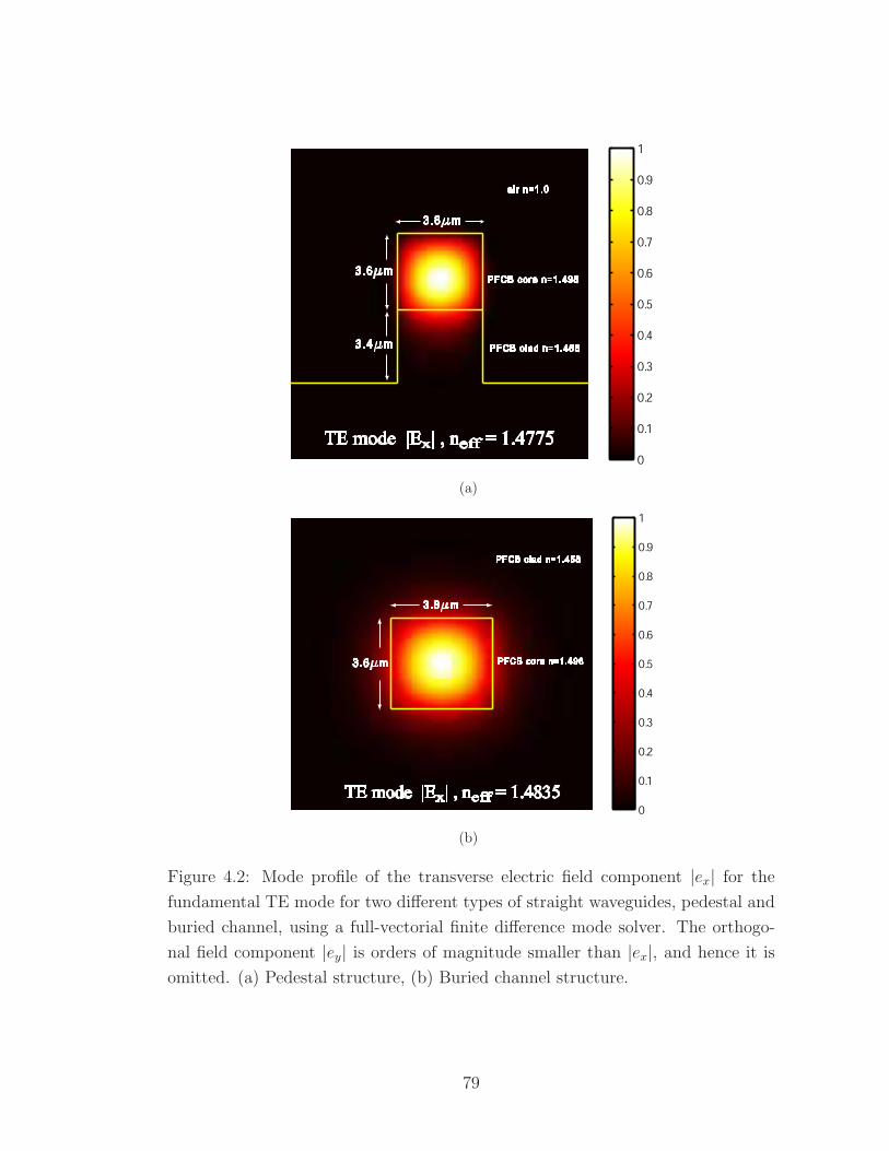
0
0.1
0.2
0.3
0.4
0.5
0.6
0.7
0.8
0.9
1
PFCB clad n=1.458
air n=1.0
3.8mm
3.6mm
TE mode |Ex| , neff = 1.4775
3.4mm
PFCB core n=1.498
(a)
0
0.1
0.2
0.3
0.4
0.5
0.6
0.7
0.8
0.9
1
PFCB clad n=1.458
PFCB core n=1.498
3.8mm
3.6mm
TE mode |Ex| , neff = 1.4835
(b)
Figure 4.2: Mode profile of the transverse electric field component |ex| for the
fundamental TE mode for two different types of straight waveguides, pedestal and
buried channel, using a full-vectorial finite difference mode solver. The orthogo-
nal field component |ey| is orders of magnitude smaller than |ex|, and hence it is
omitted. (a) Pedestal structure, (b) Buried channel structure.
79

dimensions of the core are 3.8 µm× 3.6 µm and neff is 1.48300 and 1.48297 for TE
and TM, respectively. Note that, in the buried channel waveguide, TE and TM
modes are nearly degenerate (nTEeff ≈ nTM
eff ) because it has a geometric configuration
close to that of a square and a symmetric index profile.
It is worth pointing out here that although the eigenmodes of an optical dielec-
tric waveguide are usually not pure TE or TM1, except in those two special cases
of a one-dimensional slab waveguide and an optical fiber that we mentioned above,
they are typically referred to as TE or TM modes since one of the two transverse
field components is orders of magnitude larger than the other. For example, in Fig.
4.2 the orthogonal field component |ey| is orders of magnitude (∼ 104) smaller than
|ex| in both cases and therefore it is not shown.
4.2.2 Fabrication of PFCB waveguides
This section describes the outline of the fabrication process of waveguides from
PFCB. Although the fabrication technique used here is not much different from
the ones used to build other integrated-optic waveguide devices because we adopted
an already existing conventional photolithography from the semiconductor IC in-
dustry, there are a few unique challenges to fabricating the waveguides from PFCB:
poor adhesion, a mask cracking problem, and deep etching required.
Figure 4.3 depicts an outline of the process steps to fabricate the PFCB waveg-
1In some articles or books, they are often referred to as HE/EH or Ex/Ey indicating they are
Hybrid modes. Note that the transverse electric field components |ex| and |ey| in Eq. 4.6 can
not be decoupled. Therefore, strictly speaking, TE/TM are not appropriate any more since the
solutions of eigenmode equations have both non-zero |ez| and |hz| [14, 53]
80

uides. We used Si substrates for a mechanical platform for the waveguides. In
general, fluorinated polymers have poor adhesion to other layers, which is a well-
known problem [54,55]. In order to improve the adhesion to the Si substrate, we de-
posited a 100 nm thick SiO2 layer from a Trion PECVD, after which we spin-casted
bisbenzocyclobutene (BCB, CycloteneTM 3022-35 purchased from Dow Chemical)
followed by soft curing at 210 C for 40 min as suggested by the vendor [56]. This
1 µm thick layer of BCB is believed to not only improve the adhesion strength to
SiO2/Si, but also relax the stress from the CTE mismatch between the PFCB and
the substrate. These two layers were omitted in Fig. 4.3 for clarity.
Next, solutions of PFCB cladding in mesitylene were spin-coated at a spin
speed to achieve a 7 µm thick layer and cured at 220 in the vacuum oven with
N2 environment. It is very difficult to put the PFCB core layer on top of the
PFCB cladding once the cladding layer is fully cured. This problem can be solved
with a partial curing of the cladding layer. However, when it is not cured enough,
the cladding is attacked by the mesitylene solvent contained in the core solution.
Therefore, adjusting the degree of partial curing to provide both good adhesion
and resistance to the solvent at the same time is very critical and this can be
found from trial-and-error. We have also found that dispensing mesitylene followed
by spin-drying and keeping the sample in a N2 environment for about one hour
before casting the PFCB core layer can provide an improved adhesion. After about
the 3.6 µm PFCB core layer was prepared, the sample was ready for etching the
waveguide.
81
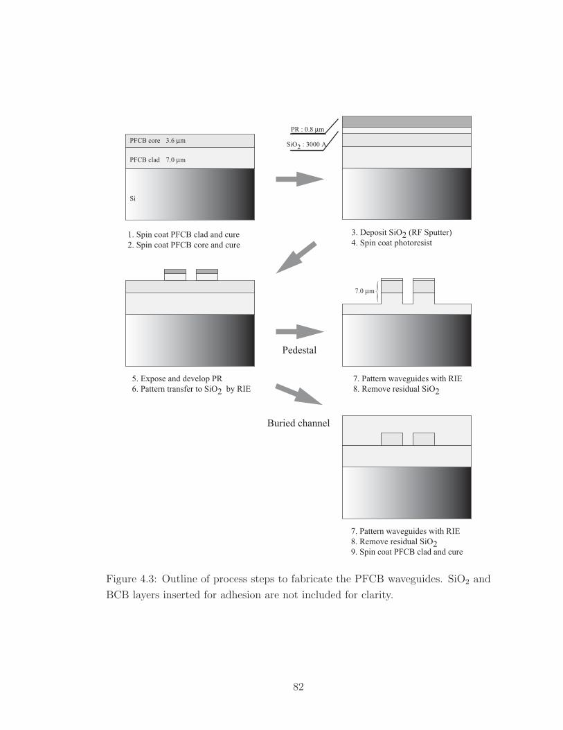
1. Spin coat PFCB clad and cure
2. Spin coat PFCB core and cure
PFCB clad
PFCB core
Si
SiO2 : 3000 A
PR : 0.8 µm
3. Deposit SiO2 (RF Sputter)
4. Spin coat photoresist
5. Expose and develop PR
6. Pattern transfer to SiO2 by RIE
7. Pattern waveguides with RIE
8. Remove residual SiO2
3.6 µm
7.0 µm
7.0 µm
7. Pattern waveguides with RIE
8. Remove residual SiO29. Spin coat PFCB clad and cure
Pedestal
Buried channel
Figure 4.3: Outline of process steps to fabricate the PFCB waveguides. SiO2 and
BCB layers inserted for adhesion are not included for clarity.
82

Because a deep etch (∼ 7 µm in the case of the pedestal structure) is required
for a waveguide structure, a hard mask was used rather than a photoresist soft
mask. For the etching mask, about a 300 nm thick SiO2 layer was deposited on
PFCB dual layers using an RF sputter deposition in an argon plasma. We used an
AJA International magnetron sputter with a chamber pressure of 3mT and an RF
power of 250 W for 70 min, resulting in a deposition rate about 43 A/min. Initially,
a layer of SiO2 from PECVD was tried for the sacrificial hard etching mask, but
it caused a severe mask cracking problem. It is believed that the SiO2 from a
magnetron sputter has a lower packing density than the SiO2 from a PECVD,
hence it is less susceptible to cracking, which is likely due to the CTE mismatch.
We also found an alternative solution of using a metal bilayer of Ni/Au that can be
patterned by deposition and lift-off. The Ni/Au etching mask can be particularly
useful for an etching mask in the case that the SiO2:cladding selectivity is poor,
for example, when a thermal SiO2 layer is used for a lower cladding.
For waveguide patterning, an 800 nm thick layer of OIR 906-10 photoresist was
exposed with a 5× GCA i-line projection aligner and developed in OPD 4262 for
60 seconds. The optimized exposure condition was found to be an expose duration
of 0.13 s and a focus offset of 0 through a focus/exposure test. Next, the waveguide
pattern was transferred to the sputtered SiO2 by reactive ion etching using a
Plasmatherm RIE system in a CHF3/O2 plasma with a flow rate of 18 sccm of
CHF3 and 2 sccm of O2, a chamber pressure of 40 mT and an RF power of 200 W,
which resulted in an etch rate of 40-45 nm/min. It should be noted that a slight
83

over etch into the core layer is required to ensure that the SiO2 has completely
cleared. After patterning the SiO2 mask, a waveguide was etched by RIE in an
Ar/O2 plasma with a flow rate of 20 sccm of Ar and 10 sccm of O2, a chamber
pressure of 20 mT, and an RF power of 250 W, which resulted in a PFCB etch
rate of 150-160 nm/min. The PFCB:SiO2 selectivity greater than 25:1. If desired,
any residual photoresist on top of SiO2 could be removed easily in acetone, but
it is not required. After the PFCB etching was completed, the remaining SiO2
was removed in a buffered oxide etch (BOE). For the buried channel waveguide
structure, the PFCB clad layer was spun and cured to serve as a top cladding layer
after patterning the core. For the final step, devices were cleaved to form smooth
end facets allowing end-fire coupling for measurements.
Figure 4.4 shows the scanning electron micrograph of the PFCB pedestal waveg-
uide. As shown in the figure, the PFCB core and clad layer are distinguishable by
exhibiting composition-dependent side wall roughness.
4.2.3 Loss measurement of straight waveguides
The loss measurement of a straight waveguide is basic but critical because one often
wants to isolate the propagation loss from total waveguide insertion loss. This
can be very helpful in designing more advanced integrated-optic devices. From
several available methods for waveguide-loss measurement, we chose the cut-back
method [57], which is the most simple and straightforward technique. A drawback
of this method is that it is a destructive measurement method requiring successive
84

Figure 4.4: Scanning electron micrograph of the PFCB pedestal waveguide.
cleaving [58]. Another popular way to measure the loss is using the properties
of Fabry-Perot resonance, because the two end facets of the waveguide form a
resonant cavity [59, 60]. However, for polymer waveguides, the reflectivity at the
air/waveguide interface is rather small and the cleaved surfaces are not quite as
perfect as those of semiconductor waveguides, so the Fabry-Perot method is less
reliable.
Figure 4.5 shows the measured total insertion loss at a wavelength of 1550 nm
for the TE mode at four different waveguide lengths achieved by sequential cleav-
ing. A single mode fiber with a conical tip (with a focal length of ∼ 8 µm) was
used to allow efficient end-fire coupling between the optical fiber and the waveg-
uide. Once the total transmission loss was measured, the coupling loss and the
propagation loss can be separated using a linear regression – the coupling loss is
85

0.0 0.2 0.4 0.6 0.8 1.0 1.22.5
3.0
3.5
4.0
4.5
5.0
5.5
6.0
pedestal
(b) 0.3 x + 2.82
(a) 1.1 x + 4.63
In
sert
ion L
oss (
dB
)
Length (cm)
buried channel
Figure 4.5: Loss measurement of PFCB straight waveguides using cutback method
for TE mode. The measured propagation loss is 1.1 dB/cm and 0.3 dB/cm, and
coupling loss is 4.63 dB and 2.82 dB for (a) pedestal and (b) buried channel waveg-
uide, respectively.
from the insertion loss at the zero waveguide length, and the propagation loss is
from the slope. The measured propagation loss was 1.1 dB/cm and 0.3 dB/cm, and
coupling loss was 4.63 dB and 2.82 dB for the pedestal and buried channel waveg-
uides, respectively. The difference in propagation loss between the two waveguides
comes mostly from a difference in scattering loss: In general, scattering loss is
larger at the waveguide side walls than at the horizontal (upper and lower) in-
terfaces because the presence of surface roughness is dominant at the side walls
86

from reactive ion etching (RIE) procedures [61, 62]. For the same reason, the side
wall roughness exhibits the polarization dependent loss (PDL) – the TE loss is
typically slightly higher than the TM loss. Furthermore, the surface-roughness-
induced scattering loss is particularly high in the case of tighter confinement of the
mode in the core as opposed to the case of weak confinement because of different
index contrast [39]. On the other hand, the coupling loss is smaller in the buried
channel waveguide because of the difference in mode mismatch between the fiber
and the waveguide [63].
4.3 PFCB Microring resonators
Devices based on a microring resonators have been actively investigated by many
research groups due to their simple configuration and yet highly interesting multi-
ple functionality. Some applications include phase shifters, optical channel drop-
ping filters (OCDF), optical add-drop (de)multiplexers, switches, photonic logic
gates, amplifiers and lasers. There are a number of excellent journal articles and
theses describing the comprehensive historical background and fundamental the-
ory on microring and microdisc resonators [64–68]. Therefore, we begin by de-
scribing a very succinct summary of the basic theoretical principles of the ring
resonator rather than a comprehensive summary, and then we discuss the design
considerations and characterization of microring resonators fabricated from PFCB
copolymers.
87

κ, τEi Et
Erb Era
(a)
κ1 , τ1Ei Et
Erd Era
κ2 , τ2
Ed Ea
Erc Erb
Drop
Input
Add
Through
(b)
Figure 4.6: Schematic diagram of microring resonators. (a) all-pass and (b) add-
drop configuration.
4.3.1 Basic principles
The microring resonator is, by nature, very similar to a Fabry-Perot resonator
in many aspects. The most simple configuration of the microring device is such
that the ring is coupled to one or two adjacent waveguides through ‘evanescent
field coupling’ as shown in Fig. 4.6. The former is often referred to as an “all-pass
88
filter” and the latter is commonly called an “add-drop filter”.
By adopting the scattering matrix formulism based on energy conservation and
time-reversal symmetry [69], the relationships between the optical electric fields for
the add-drop filter, shown in Fig. 4.6, can be written as
Ea
Et
=
τ1 −jκ1
−jκ1 τ1
Erd
Ei
, (4.7)
Ed
Erc
=
τ2 −jκ2
−jκ2 τ2
Erd
Ei
. (4.8)
We can also write equations describing the circulation condition along the ring,
Erb = Era ·√
A · ejφ/2, (4.9)
Erd = Erc ·√
A · ejφ/2, (4.10)
where A = exp (αRL/2) represents the field loss (or gain) after one round-trip,
φ = k0neffL is the round-trip phase change, αR is the power loss coefficient in the
ring, neff is the effective index of the waveguide, L = 2πR is the circumference of
the ring, κ(1,2) are the field coupling coefficients between the bus and the ring, and
τ(1,2) are the field transmission coefficients. We also assume a lossless coupling, in
which case τ(1,2) =√
1 − κ2(1,2).
Therefore, from Eqs. 4.7–4.10, the optical fields at drop port Ed and through
89

port Et can be expressed as,
Et =τ1 − τ2Aejφ
1 − τ1τ2AejφEi +
−κ1κ2
√Aejφ/2
1 − τ1τ2AejφEa, (4.11)
Ed =−κ1κ2
√Aejφ/2
1 − τ1τ2AejφEi +
τ2 − τ1Aejφ
1 − τ1τ2AejφEa. (4.12)
When there is no input signal at the add port, i.e. Ea = 0, Eqs. 4.11 and are
reduced to
Et
Ei
=τ1 − τ2Aejφ
1 − τ1τ2Aejφ, (4.13)
Ed
Ei
=−κ1κ2
√Aejφ/2
1 − τ1τ2Aejφ. (4.14)
The optical field at the through port Et for the all-pass configuration can be
obtained by putting τ1 = τ and κ1 = κ, and letting κ2 = 0 in Eq. 4.13 because there
is no second waveguide adjacent to the ring. Then, for the all-pass configuration,
we have
Et
Ei
=τ − Aejφ
1 − τAejφ(4.15)
=A − τejφ
1 − τAejφ· ej(π+φ). (4.16)
The phase of Et can be obtained from Eq. 4.16 and can be written as,
Φ =τ − Aejφ
1 − τAejφ. (4.17)
For the all-pass configuration, when the ring resonator is lossless, i.e. A = 1, (but,
in practice, this has to be the negligible loss case, A ≈ 1) the output power is unity
(100% transmission) at all wavelengths regardless of the coupling coefficient κ. On
90

1535 1540 1545 1550 1555 156010
2
10 1
100
Wavelength (nm)
No
rma
ilize
d in
ten
sity
, |
Et|2
Figure 4.7: Calculation of a typical spectral response of all-pass filter with neff =
1.477, R = 30 µm, and τ = 0.9 for when A = 1 and A = 0.9 representing the
lossless case and the round-trip power loss of 19%, respectively.
the other hand, when the ring has a finite amount of loss that satisfies “critical
coupling”, in which the round trip field loss of the ring equals the field coupled into
the ring from the bus waveguide, i.e. A = τ , the output power has high extinction
at the resonant wavelengths. This could be used as an optical channel-drop filter
(OCDF), also referred to as a notch filter. Figure 4.7 shows the calculation of a
typical spectral response of an all-pass filter with neff = 1.477, R = 30 µm, and
τ = 0.9 when A = 1 and A = 0.9 representing the lossless case and the round-trip
power loss of 19%, respectively.
Although the all-pass configuration with a negligible loss is not useful as a
91

φ = δ (ωT)
Pha
se S
hift,
θ
2π
π
0 0 −π/4 π/4
τ = 0.99
τ = 0.90
τ = 0.95
A = 0.99
Figure 4.8: Calculated phase response near a resonance in all-pass configuration
for three different τ ’s when the loss is very small, A = 0.99.
channel drop filter, its interesting phase response near the resonant wavelength
(φ ≈ 0), as shown in Fig. 4.8, makes it possible for use as a π phase shifter. This
can be utilized as a notch filter by incorporating it into one arm of a Mach-Zehnder
interferometer [66]. The add-drop configuration is mathematically equivalent to
a Fabry-Perot interferometer with two input and two output ports. Using the
narrow-band amplitude filter response from its high wavelength selectivity, one
can drop a particular frequency band from the input port via the drop port and
add another band from the add port to the through port. Figure 4.9 shows a
typical spectral response of an add-drop filter with neff = 1.477, R = 30 µm,
A = 0.95, and τ1 = Aτ2 = 0.9 satisfying the critical condition. Resonators are
92

1542 1544 1546 1548 1550 1552 1554 1556 1558 156010
3
10 2
10 1
100
Wavelength (nm)
Norm
aili
zed in
tensi
ty
Figure 4.9: Calculation of a typical spectral response of add-drop filter with neff =
1.477, R = 30 µm, A = 0.95, and τ1 = Aτ2 = 0.9 satisfying the critical condition.
typically characterized by their free spectral range ∆νFSR (or ∆λFSR), resonance
width ∆νFWHM (or ∆λFWHM, the full width at half maximum), quality factor Q,
and finesse F . The free spectral range is the separation between two successive
resonances expressed as,
∆νFSR =c
Lneff
=1
Tin frequency, (4.18)
∆λFSR =λ2
0
Lneff
in wavelength, (4.19)
and the finesse F is defined as
F =∆νFSR
∆νFWHM
(4.20)
93

The quality factor Q, describing the rate at which the resonator dissipates its stored
energy and the sharpness of a resonance, is defined as the resonance frequency
divided by the bandwidth, Q = ν0/∆νFWHM, and is related to the finesse by
Q = LneffF/λ.
4.3.2 Design considerations
Mode analysis
In section 4.2.1, we discussed the eigenmodes of the dielectric waveguides and nu-
merically computed the eigenvalue equation to find the eigenmodes for a given
waveguide geometry. The numerical mode profile that we obtained can also be
used to compute the scattering loss at the waveguide boundary or the coupling
efficiency between two adjacent waveguides. To construct the microring resonator
devices, the pedestal waveguide structure was adopted simply because it allows
the most tightly confined guiding geometry.
Bending Loss
The most commonly used practical figure of merit for a ring resonator is the quality
factor or finesse, which is directly related to the radius of the ring, the propaga-
tion loss in the ring, and the coupling efficiency between the ring and waveguide.
Obtaining loss as low as possible is essential because the loss directly dictates the
resonance bandwidth (FWHM), hence Q and F of the ring resonator. Two main
contributions to loss in the ring are bending loss and scattering loss. For a given
index contrast of the waveguide, one can simply increase size of the ring and in-
94

crease etching depth of the pedestal structure in order to minimize the bending
loss.
For the PFCB microring devices, the waveguide dimensions in Fig. 4.2(b) and a
radius of curvature R in the range of 25–40µm are chosen from detailed numerical
modelling for the bending loss. There is a simple model to calculate bending loss
in planar slab waveguides based on Fraunhoffer diffraction theory [70]. This model
can be very useful especially in the early phase of the design by providing a good
starting point for determining a radius of curvature and width of the waveguide.
However, for most practical waveguides with a 3D structure confining the lightwave
both horizontally and vertically, this is only an good approximation.
We performed a 3D full vectorial FD calculation incorporating a conformal
transformation and a complex perfectly matched layer (PML) [71–73]. Figure 4.10(a)
shows that a radius R of 30 µm with an etch depth 7 µm is estimated to yield neg-
ligible bending loss (< 10−3 dB). Figure 4.10(b) shows the etch depth dependence
from the calculation of the bending loss with several different etch depths when
R = 30 µm. The round-trip power loss A2(= exp (αRL)) as a function of etch
depth h can be fitted to an exponential curve, i.e. A2 = 1 − e−2.2h. It should
be noted that this dependence could almost be predicted from the fact that the
field decay constant in the lower cladding layer, k0
√
n2eff − n2
s, is about 1.13 when
neff = 1.4775, and the power decay constant is twice as much.
95

µm
µm
A2 = 0.99978
-60dB
PML layer
(a) Bending loss when R = 30µm
4 4.5 5 5.5 6 6.5 70
0.2
0.4
0.6
0.8
1
Etch depth ( µm)
Ro
un
d t
rip
po
we
r lo
ss (
A2)
e-2.2h
(b) Etch depth dependence
Figure 4.10: 3D full vectorial calculation for a bending loss. (a)negligible bending
loss < 10−3 dB when a radius R of 30 µm with a etch depth of 7 µm, and (b)Etch
depth dependence of the bending loss when R = 30 µm. The round-trip power
loss A2 as a function of the etch depth h can be fitted to an exponential curve,
A2 = 1 − e−2.2h.
96

Coupling efficiency
One of the most important design parameters for constructing a practical microring
resonator device is the coupling efficiency – the amount of power transferred from
one waveguide to another when they are in close proximity – between the waveguide
and the ring. From this, we can determine the physical size of the gap required
for the critical coupling condition.
In a system consisting of two adjacent waveguides, the coupling constant be-
tween the two can be numerically computed from the mode profile we obtained
before and the coupled-mode theory [52, 74]. A very comprehensive and excellent
summary on non-orthogonal coupled-mode theory can be found in [52]. Therefore,
in this section, we present only the computation results for the coupling constant
µ in the coupled-mode equation,
d
dz
a1(z)
a2(z)
= −j
β1 µ12
µ21 β2
a1(z)
a2(z)
, (4.21)
where β1 and β2 are the propagation constants of waveguide 1 and waveguide 2,
respectively.
When the two waveguides are identical to each other, we can calculate the
coupling constant in a more direct way by considering the coupled waveguide
system as a whole rather than as two separate waveguides. The approximate
normal modes of the system can be expressed as the symmetric and antisymmetric
97

g
PFCB clad, n = 1.458
PFCB core, n = 1.498
air, n = 13.6 µm
3.6 µm
3.4 µm
Figure 4.11: Cross-sectional mode profile of two parallel waveguides separated by
an edge-to-edge distance g.
combinations of the isolated waveguide modes as
βs = β + µ, vs =1√2
=
+1
+1
, (4.22)
βa = β − µ, va =1√2
=
+1
−1
. (4.23)
Therefore, the coupling constant µ can be written as
µ =1
2(βs − βa). (4.24)
Figure 4.11 shows the mode profile of two parallel PFCB pedestal waveguides
separated by an edge-to-edge distance g, which was used to compute the coupling
98

0 0.2 0.4 0.6 0.8 1 1.2 1.4 1.6 1.8 210
−6
10−5
10−4
10−3
10−2
Coupling gap (µm, edge to edge)
Cou
plin
g co
nsta
nt,
µ (
µm
−1 )
Non−orthogonal Coupled Mode TheoryExact Mode Analysis
Figure 4.12: Calculation of coupling constant between two PFCB pedestal waveg-
uides as a function of waveguide separation g.
constant. Figure 4.12 shows the calculated coupling constant µ between two PFCB
pedestal waveguides as a function of waveguide separation g from both the non-
orthogonal coupled theory and the direct mode analysis. Note that the coupling
constant µ drops exponentially with increasing separation g, as we expect from
the fact that electric field decays exponentially in the cladding region. Also note
that the direct modal evaluation agrees very well with the coupled mode theory,
especially when g > 0.3 µm.
In order to find the field coupling coefficient κ in Eqs. 4.13–4.16, we consider
99

the transfer matrix, which is the solution of the differential coupled mode equation:
a1(z)
a2(z)
= ejβ0z
cos σ(z) − sin σ(z)
− sin σ(z) cos σ(z)
a1(0)
a2(0)
, (4.25)
with
σ(z) ≡∫ z
0
µ(z) dz, (4.26)
where σ(z) represents the integrated coupling when the two waveguides approach
and separate gradually as in the microring resonator. If light is launched into
waveguide 1 at z = 0, then the relative power in the two waveguides as a function
of z is given by,
∣
∣
∣
∣
a2(z)
a1(0)
∣
∣
∣
∣
= sin σ(z), (4.27)
∣
∣
∣
∣
a1(z)
a1(0)
∣
∣
∣
∣
= cos σ(z). (4.28)
Therefore, the coupling coefficient κ between the ring and the bus waveguide is
κ = sin σ(z) (4.29)
≈ σ(z) when σ(z) ≪ 1. (4.30)
4.3.3 Experimental characterization
The fabrication process to build the PFCB microring resonators is almost identical
to the one described in section 4.2.2. Effort was made to achieve a coupling gap
g as small as possible. The limitation on the coupling gap comes mainly from
the following two causes. First, the smallest feature size is fundamentally limited
by the wavelength of the light source employed in the i-line (λ = 365 nm from
100

Mercury lamp) projection aligner we used for photolithography. Second, the tight
confinement of guided light to reduce the bending loss requires a deep etch into
the cladding layer as we discussed earlier. In general, a high RF power and low
chamber pressure can increase the anisotropicity (or verticality) in RIE etching,
but the side wall etching to a certain degree is unavoidable. Figure 4.13 shows
a scanning electron micrograph of a PFCB add-drop microring resonator with a
radius of 25µm and a coupling gap of 0.45 µm. A coupling gap down to 0.4 µm
with our stepper is possible, but it is very difficult to achieve.
Figure 4.14 illustrates the experimental setup for characterizing the microring
devices. We used a Photonetics tunable laser and/or an erbium doped fiber am-
plifier (EDFA) for light sources. Light was coupled into the waveguide using a
conical-shaped lensed fiber, which has a focal length of approximately 8 µm. A
signal emerging from either the through port or the drop port is collected by a
lensed fiber and directed to a detector and a spectrum analyzer. Both the input
and output fibers are mounted on 3-axis translation stages from Newport, allowing
accurate and stable alignment.
Using a broad band amplified spontaneous emission (ASE) from an EDFA as
a light source can be very useful for device alignment because a spectrum ana-
lyzer allows us to monitor the spectral response of the device in nearly real-time.
Figure 4.15 shows the dropped signal at the drop port of an add-drop filter with a
radius of 25µm when the ASE light is coupled into the input port. As shown in the
figure, the measured free spectral range λFSR = 9.3 nm. Note that the unpolarized
101

µ
µ
Figure 4.13: Scanning electron micrograph of PFCB ring resonator, with a radius
R = 25 µm, and a coupling gap g = 0.45 µm.
102

Tunable Laser Isolator
Polarization Controller
Lensed Fiber
Power-meterDetector
EDFA
Wavemeter
Lensed Fiber
Spectrum
Analyzer
GPIB
Figure 4.14: Experimental setup for microring characterization.
ASE source shows the resonances for both TE and TM mode, and the different
signal intensities for TE and TM can be explained by the polarization dependent
scattering loss (PDL) and the difference in coupling constants.
Figure 4.16 plots the normalized signal of the device at the through and drop
port at the resonance at 1531.05 nm from a tunable laser input. As shown in
the figure, the maximum extinction ratio at the throughput port is 4.87 dB, and
the calculated quality factor Q and finesse F are approximately 8544 and 55,
respectively.
In addition, we observed a resonance shift with increasing EDFA input power.
When the total ASE power was increased from 4 dBm to 12 dBm, a resonance shift
103

1520 1530 1540 15500.0
5.0x10⁻⁸
1.0x10⁻⁷
1.5x10⁻⁷
2.0x10⁻⁷
Wavelength (nm)
Inte
nsity
0.0
1.0x10⁻⁹
2.0x10⁻⁹
3.0x10⁻⁹
TE
TM
R = 25 µm
∆λFSR = 9.3 nm
Figure 4.15: Measured spectral response at the drop port of a add-drop filter with
a radius 25µm with ASE input (solid line). The measured free spectral range λFSR
is 9.3 nm for TE mode. EDFA spectrum (dotted line) is also plotted as a reference.
104

1530 1530.5 1531 1531.5 15320
0.2
0.4
0.6
0.8
1
Wavelength (nm)
Norm
aliz
ed in
tensi
ty
Throughput
Drop
Figure 4.16: Normalized signal of the device at the throughput and drop port at
the resonance at 1531.05 nm from a tunable laser input.
of 25 pm was obtained as shown in Fig. 4.17(a). We speculate that the origin of
this resonance shift is thermal, based on the observation of the negative thermo-
optic coefficients, dn/dT , of the PFCB polymers as shown in Fig. 4.17(b). The
thermo-optic coefficient was obtained by measuring refractive indices at different
temperatures with a MetriconTM that was custom fitted with temperature con-
trol. This negative dn/dT that lowers the mode effective index of the waveguide
can qualitatively explain the blue-shift of the resonance with increasing EDFA
input power. Similar effects were observed in microrings fabricated from benzocy-
clobutene (BCB) polymer, and optical bistable switching based on the resonance
105

shift was demonstrated by other members in our group [75,76]. They are currently
investigating the subject for more complete understanding of the physical origin.
4.3.4 Ultrafast all-optical switching experiment
More than two decades ago, ultra-fast optical control of microwave and millimeter
wave propagation was reported [77, 78]. This ground work demonstrated phase
shifting, switching, and modulating in semiconductor waveguides using a picosec-
ond laser pulse. Likewise, the light signal out of a microring can also be modulated
or switched by changing the optical properties of the material with an optical pump
that either co-propagates through the ring together with a probe signal [79, 80],
or directly illuminates the ring from above. All-optical lightwave switching in
GaAs semiconductor microring devices was also achieved by injecting free carriers,
generated by absorbing photons with an energy greater than the band gap [81].
In this section, we show that all-optical switching in polymer microrings is
possible from preliminary experimental results. The fundamental physics of car-
rier dynamics in polymer devices is substantially different from the direct optical
excitation of electrons and holes for the GaAs semiconductor microring devices.
Although it is not clearly understood at this point, the all-optical switching we
observed can still be explained by carrier injection (excitons and free carriers),
as evidenced by an earlier report on the transient photoconductivity in a BCB
polymer film induced by a femtosecond laser pulse [82].
For the switching experiment, we used a microring-loaded Mach-Zehnder inter-
106

1533.2 1533.4 1533.6 1533.8 15340
0.5
1
1.5
2x 10
−8
Wavelength (nm)
Inte
nsity
4 dBm 6 dBm 8 dBm10 dBm12 dBm
(a) ASE input power vs. resonance shift
20 40 60 80 100 1201.45
1.46
1.47
1.48
1.49
1.50
1.51
PFCB clad, dn/dT = -5.95x10⁻⁵ oC
-1
PFCB core, dn/dT = -9.13x10⁻⁵ oC
-1
Index o
f R
efr
action
Temperature (oC)
(b) Thermo-optic coefficient, dn/dT
Figure 4.17: (a) Resonance shift with increasing ASE input power. Maximum
resonance shift 25 pm obtained. (b) Thermo-optic coefficient, dn/dT , measured
using a MetriconTM that was custom outfitted with temperature control.
107

ferometer (MR-MZI) – a microring coupled to one arm of an MZI – fabricated from
PFCB, which is schematically shown in Fig. 4.18(a). In the experiment, a train of
mode-locked Ti:Sapphire laser pulses with a pulse width of 100 fs, a repetition rate
of 1 KHz at a wavelength of 400 nm was used for the optical pump beam. When
these pump pulses directly illuminate the ring from above, it causes a temporal
blue shift of the microring resonance as schematically shown in Fig. 4.18(b). When
the probe beam is initially tuned to a wavelength slightly shorter than a ring res-
onance (λ1p < λR in Fig. 4.18(b)), the probe beam experiences a rapid decrease
in transmission temporally due to the resonance shift from λR to λ′R, and hence
exhibits High-Low-High modulation behavior. On the other hand, when the probe
beam is initially tuned to a resonance (λ2p = λR in Fig. 4.18(b)), the probe beam
experiences a rapid increase in transmission, and hence exhibits Low-High-Low
modulation behavior. As a result, the train of pulses modulates the probe signal
in time as shown in Fig. 4.18(d) and (e), respectively.
In addition to this amplitude modulation from the resonance shift, the opti-
cal pump pulse changes the phase near a ring resonance as we discussed in sec-
tion 4.3.1. Fig. 4.18(c) illustrates the phase response across the resonance. For
an MR-MZI, the temporal π phase shift around a resonance of the ring resonator
can destructively interfere with the light in the second arm, therefore, as in the
amplitude modulation, the train of pulses modulates the probe signal in time as
shown in Fig. 4.18(d) and (e), depending on whether the probe signal is initially
on-resonance or off-resonance. From the combined effect of amplitude modulation
108

Low-High-Low t
I
I
λλRλR'
H
φ = δ (ωT)
Ph
ase
Sh
ift,
θ
2π
0
0 /4 /4 −π π
t
I
LH L
H
H
(a)
(b) (c)
High-Low-High
(d) (e)
π
λp
1 λp2
L
Figure 4.18: Schematic picture of all-optical switching experiment. (a)An optical
pump with a 100 fs Ti:Sapphire laser pulse with an energy of 500 pJ/pulse at 400 nm
directly illuminates the ring from above. The resulting modulation behavior comes
from the combined effect of (b) amplitude and (c) phase modulation. (d),(e)
Therefore, the probe signal is modulated in time H-L-H or L-H-L depending on
the initial probe wavelength.
109

and phase modulation, the switching efficiency can be greatly increased around
the resonance [83,84]. However, it should be noted that this phase contribution is
significant only when the one arm of the MZI is over-coupled to the ring and the
loss in the ring is negligibly small.
The transfer response at the output of an MR-MZI is given by
Et =Ei
2
|Er|ejΦej∆φ + 1
(4.31)
where Er and Φ were given by Eqs. 4.16 and 4.17, respectively, and ∆φ is the phase
imbalance between the two arms of the MZI. Note that a finite imbalance in length
between two arms of an MZI resulting from fabrication imperfection is inevitable
and the phase difference (∆φ = k0neff∆d) from the length imbalance (∆d) can
greatly affect the spectral response of an MR-MZI over a wide range of wavelengths.
The spectral response of an MR-MZI shown in Fig. 4.19 is exaggerated for the case
of a length imbalance, ∆d = 5 µm, and a ring radius, R = 10 µm. As shown in
the figure, when the phase difference between the two arms is close to ∆φ = π,
the ring resonances exhibit ‘peaks’ rather than ‘dips’, and when 0 < ∆φ < π, the
resonance dips show asymmetric profiles. However, the ∆d can easily be controlled
to less than 100 nm, and therefore the response from an MZI without a microring
is essentially flat over a narrow range of wavelengths in most cases.
Figure 4.20 shows the preliminary experimental data showing the modulation
(or switching) response of the device (R = 50 µm) when a 100 fs Ti:Sapphire laser
pulse with an energy of 500 pJ/pulse was used for an optical pump beam. By
110

1300 1400 1500 1600 1700
0.2
0.4
0.6
0.8
Wavelength (nm)
Norm
aliz
ed in
tensi
ty
∆φ = 0
∆φ = π
Figure 4.19: Spectral response of an MR-MZI with a length imbalance between
two arms of the MZI, ∆d = 5 µm, which is exaggerated for clarity. The microring
is critically coupled and has a round-trip loss, A = 0.95, an effective index, neff =
1.477, and a radius of the ring, R = 10 µm.
111

sweeping the wavelength of a probe beam across a ring resonance (λR ≈ 1554.9 nm)
and detecting the time variation of the transmitted signal, we can estimate how
much the resonance is shifted. As shown in the figure, when the probe beam
was initially tuned to a wavelength slightly shorter than a ring resonance, and
progressively scanned towards the resonance, the dropped probe beam exhibited
High-Low-High modulation behavior. On the other hand, when the probe beam
was initially tuned to the resonance and scanned away from the resonance, the
signal is modulated as Low-High-Low. As discussed before, this can be explained
by the temporal change in the optical properties of the PFCB polymer. A response
pulse width of about 30 ps, which is primarily limited by the sampling scope used
in the measurement, and a maximum modulation depth of 3.8 dB was obtained.
Note that the response window is wider in the case that the probe wavelength was
scanned away from the ring resonance because of the asymmetric resonance profile
arising from length imbalance as shown in Fig. 4.19.
The estimated resonance shift ∆λ is around 0.6 nm, leading to a maximum
refractive index change, ∆n ≈ −5.7×10⁻⁴. From the pulse energy of 500 pJ/pulse
used in the experiment, if this resonance shift results from the intensity dependent
nonlinear refractive index, n = n0 +n2I, from 3rd order nonlinear optical effect, an
n2 on the order of −8× 10⁻¹⁸ m2/W, and a |Reχ(3)| on the order of 4× 10⁻⁹ esu
would be required. This large value of χ(3) is much higher than one might expect
from PFCB, therefore it can be speculated that the observed behavior results from
exciton and/or free carrier effects as we observed in the GaAs microring devices.
112

0 500 1000 1500 2000
0
2
4
6
8
10
12
Outp
ut S
ignal (m
V)
Time (ps)
1554.00 nm
1554.25 nm
1554.50 nm
1554.75 nm
(a) towards resonance
0 500 1000 1500 2000
0
2
4
6
8
10
12
Outp
ut S
ignal (m
V)
Time (ps)
1555.00 nm
1555.25 nm
1555.50 nm
1556.0 nm
(b) away from resonance
Figure 4.20: Measured switching response of the MR-MZI when the ring was
illuminated by a 100 fs Ti:Sapphire laser pulse with an energy of 500 pJ/pulse at
400 nm. The probe signal was swept through one of the ring resonances, λR ≈1554.9 nm.
113

However, the switching efficiency is about two orders of magnitude worse than
for the GaAs devices, mainly from the following two reasons. First, the carrier
generation efficiency is worse than the one from the conduction–valence interband
transition from linear absorption in the GaAs device. Second, a phase contribution
to switching is not significant because the ring in our case is under-coupled to the
MZI and the loss present in the ring cannot be neglected. Figure 4.21 shows a
phase response around a resonance for the all-pass configuration with a round-
trip field loss A = 0.9 when the field transmission coefficients are τ = 0.95 and
τ = 0.98. When the ring is lossy, particularly when the coupling efficiency is very
small compared to the loss (for example, solid line in the figure, a round-trip power
loss of 19% and a power coupling efficiency of 4%), the effective phase shift Φ shows
a very different behavior from the one we discussed in section 4.3.1 and it is much
smaller than a radian. Therefore, the phase modulation represented by ejΦ term
in Eq. 4.31 is not significant.
4.4 Summary
In this chapter, we investigated low-loss waveguides and microring resonators fabri-
cated from perfluorocyclobutyl (PFCB) copolymer. Fluorinated polymers are one
of the most attractive materials to construct photonic passive waveguides because
they have substantially low absorption loss at telecommunication wavelengths.
Low-loss waveguides are one of the most important building blocks in integrated-
optic communication systems because most passive and active devices consist of
114

−0.8 −0.6 −0.4 −0.2 0 0.2 0.4 0.6 0.8
−0.2
−0.1
0
0.1
0.2
Normalized detuning, δ(ωT)
Effe
ctiv
e ph
ase
shift
, Φ
A = 0.9
τ = 0.98
τ = 0.95
Figure 4.21: Calculated phase response near a resonance in all-pass configuration
when the ring is lossy and under-coupled, a round-trip field loss A = 0.9, the field
transmission coefficients are τ = 0.95 and τ = 0.98.
115

simple straight and curved waveguide segments. For example, microring resonator
based devices have very simple configurations of straight waveguides and circular
rings, and the loss present in the ring is the most important parameter determin-
ing the device performance. For these reasons, this chapter was devoted to the
design, fabrication, and characterization of those devices using PFCB polymers.
We demonstrated straight waveguides with propagation losses of 0.3 dB/cm and
1.1 dB/cm for a buried channel and pedestal structures, respectively, and a mi-
croring add-drop filter with a maximum extinction ratio of 4.87 dB, quality factor
Q = 8554, and finesse F = 55. In addition, we showed that all-optical switching
with the PFCB microring resonator is possible when it is optically pumped by
a femtosecond laser pulse with sufficient energy. From a microring-loaded Mach-
Zehnder interferometer (MR-MZI), we demonstrated that a modulation window of
30 ps and modulation depth of 3.8 dB from an optical pump with a pulse duration
of 100 fs and pulse energy of 500 pJ when the signal wavelength is initially tuned
to one of the ring resonances.
116

Chapter 5
Organic Thin-Film Photodetector
based on Bulk Heterojunction
Ever since the discovery of organic semiconducting polymers1, new avenues for
their use as replacement for inorganic semiconductors have been explored. This
interest is fueled by their potential capabilities and possibilities for modern elec-
tronic and photonic devices, which include light emitting diodes (LEDs) [85, 86],
photovoltaic cells (PVs) [87–90], photodetectors (PDs) [91–94], and field effect
transistors (FETs) [95–98]. Among these, development of OLEDs has nearly ma-
tured and they were recently employed in the commercial flat panel displays for
small electronic appliances such as cell phones and PDAs. The commercial success
of this technology provided further spur to research on organic photovoltaic cells
in particular and organic photodetectors to a lesser extent because of their very
low manufacturing cost and substrate flexibility. Because solar energy conversion
in OPV cells and light detection in OPDs share a lot of common basic physics,
the work on organic thin film photodetectors that we discuss in this chapter has
benefited from the ideas developed in the study of OPV cells.
1This pioneering work on the discovery and development of electrically conductive polymers
by Alan J. Heeger, Alan G. MacDiarmid, and Hideki Shirakawa was awarded the Nobel Prize in
Chemistry in 2000 [3]
117

5.1 Basic principles
Charge carrier transport and light absorption in organic semiconducting materials
are associated with electronic bands formed by sp2-hybridized orbitals of carbon
atoms. An electron in the pz-orbital of each sp2-hybridized carbon atom will form
π-bonds with neighboring pz electrons. In conjugated polymers with chains of
alternating single–double bond structure, the molecular pz orbitals constituting
the π-bonds are actually overlapped and spread over the entire molecule. The
electrons in this molecular orbital are respectively delocalized along the whole
molecular chain, resulting in high electron polarizability.
Organic semiconducting polymers have a few distinct features, which distin-
guish them from their crystalline inorganic counterparts. First, organic materials
have poor carrier mobilities, typically less than 1 cm2/V ·s in most materials, which
is orders of magnitude lower than inorganic semiconductors. The highest mobility
reported to date is around 5 cm2/V · s in the pentacene-based field effect transistor
through a surface modification [98], and yet this is still two orders of magnitude
lower than silicon. Second, most organic semiconductors have absorption peaks
located in the visible range with strong absorption coefficients typically greater
than 105 cm−1. In most practical devices, however, this high extinction requires
an active layer thicknesses of only a few hundred nanometers, which partly com-
pensates for the low mobilities. Third, the absorption of incident photons in these
materials lead to photo-excitation of excitons (referring to mobile excited states or
118

S
S
S
S
*
*n
P3HT
PCBM-C60
e-
hν
OMe
O
Figure 5.1: Schematic drawing illustrating photoinduced charge transfer between a
conjugated polymer (P3HT) and a fullerene (PCBM-C60). After photo-excitation
P3HT, the electron is transferred to the PCBM-C60 within 10−13 second. With
respect to electron transfer, they are often referred to as donor and acceptor ma-
terials. In this particular example, P3HT is an electron donor and fullerene is an
electron acceptor material.
bound electron-hole pairs via the Coulomb force) rather than free charge carriers.
These excitons, an intermediate product in the photocurrent generation process,
carry energy but no net charge. Hence they diffuse within the material as a single
entity and recombine within distances, typically on the order of 10 nm [99–101].
In solar cells or photodetectors, they need to be dissociated non-radiatively by an
applied electric field exceeding the exciton binding energy, which can be up to 2 eV,
or through a process called photoinduced charge transfer [102–105], after which
free carriers can be collected at the respective electrodes.
119

Several approaches of active layer composites for organic PV cells or detectors
have been made over the last few decades. The main concepts of these approaches
are fundamental photophysics based on the photoinduced charge transfer either be-
tween layers of conjugated polymers and low molecular weight organic molecules
forming a single heterojunction at the interface, or within a single layer blend
of conjugated polymers and low molecular weight organic molecules forming a
bulk heterojunction. The very first generation of organic thin film PV cells was
based on a single organic layer sandwiched between two metal electrodes of dif-
ferent work functions [88], but the external quantum efficiency (EQE) and hence
the power conversion efficiency (PCE) was very poor, generally ≪ 1%. The re-
markable breakthrough was achieved by introducing bilayer heterojunction and
bulk heterojunction devices consisting of buckminster fullerene C60 molecules or
soluble derivatives of C60 in addition to the active conjugated polymers. After
photo-excitation of the conjugated polymer by an incident light with an energy ~ω
greater than the π-π∗ gap, electrons are transferred onto the fullerene molecules due
to their high electron affinity. Because an electron is transferred from the p-type
hole conducting polymer to the n-type electron conducting C60, these materials are
often referred to as electron donors and electron acceptors, respectively. Fig. 5.2(a)
illustrates a schematic energy band diagram of electrodes with their work-functions,
and donor/acceptor materials with their ionization potential Ip, electron affinity
χ, and energy band-gap Eg between HOMO (highest occupied molecular orbital)
and LUMO (lowest unoccupied molecular orbital) levels corresponding to the va-
120

lence and conduction bands in inorganic semiconductors, respectively. For efficient
charge transfer, an exciton binding energy greater than IDp −χA
p is required because
it is energetically favorable. Detailed time-resolved studies on this photoinduced
charge transfer between conjugated polymers and fullerene molecules showed that
it occurs within 10−13 second after photo-excitation of the polymer, which is nearly
103 faster than any other competing process [106]. For this reason, the charge
transfer efficiency approaches 100%, resulting in excellent quenching of excitonic
photoluminescence from the polymer.
Figure 5.3 depicts conceptually the photoinduced charge transfer in bilayer and
bulk heterojunction structures. In the bilayer structure, where the electron donor
(p-type hole conducting polymer) and electron acceptor (n-type electron conduct-
ing fullerene) form a well-defined planar interface by sequential deposition or spin-
casting of the organic layers, the EQE and PCE are limited primarily by the exciton
lifetime before photoexcited excitons recombine or dissociate into free charge carri-
ers at the D-A interface. Therefore, the device thickness should be kept within the
exciton diffusion length of the active polymer material for efficient charge trans-
fer. On the other hand, in the bulk heterojunction device, the D-A interface is
distributed over the entire active layer structure because both donor and acceptor
materials are co-evaporated or blended in solution. Therefore, the interfacial area
is increased by a large extent such that the dissociation site at a D-A interface falls
within a distance closer than the exciton diffusion length from an each absorbing
site. For this reason, the charge generation efficiency in the bulk heterojunction
121

hν
+
−
−
+
Ebi
EF1
IPD
IPD
IPA
IPA
EF2
χA
χA
χD
χD
EgD
EgD
EgD
EgD
(a)
(b)
ηA
ηED
ηCT
ηCC
+
−
Figure 5.2: (a) Schematic energy level diagram of electrodes with Fermi energy,
and a donor and acceptor materials with energy band-gap Eg between HOMO and
LUMO, ionization potential Ip and electron affinity χ. For efficient charge transfer,
an exciton binding energy greater than IDp −χA is required. (b) Schematic illustra-
tion of photocurrent generation in heterojunction PV cells and PDs. Generation of
photocurrent consists of four steps: exciton generation, exciton diffusion, exciton
dissociation by photoinduced charge transfer, and free charge carrier collection at
the electrodes. Therefore, the external quantum efficiency, the ratio of the number
of free charge carriers to the number of incident photons, can be expressed with
four respectively corresponding efficiencies, ηA, ηED, ηCT, ηCC.
122
structure is known to be near 100%. However, in such a blended structure, effi-
cient charge transport to the electrodes is sensitive to the nanoscale morphology
of the mixture because it requires an intimate interpenetrating network to pro-
vide percolated pathways for the hole and electron conducting paths to reach the
opposite contacts. Nanomorphology is dependent on many parameters: an evap-
oration rate, substrate temperature during vacuum deposition process, specific
solvents used and solvent evaporation time for solution process like spin-casting,
and the annealing condition and relative concentration of the mixture for both
processes [90]. It should be noted that charge transport in actual devices can be
much more complicated than the continuous conducting paths as illustrated in
Fig. 5.3(b) [107].
Photocurrent generation in heterojunction PV cells and PDs consists of four
steps and the corresponding efficiencies are defined as:
1. Exciton generation in the electron donor material from incident photons,
which is directly related to the material absorption coefficient, (ηA).
2. Exciton diffusion, fraction of excitons generated in the donor material reach-
ing the D-A interface, (ηED).
3. Exciton dissociation at the D-A interface through photoinduced charge trans-
fer, (ηCT).
4. Charge collection at the electrodes, (ηCC).
123
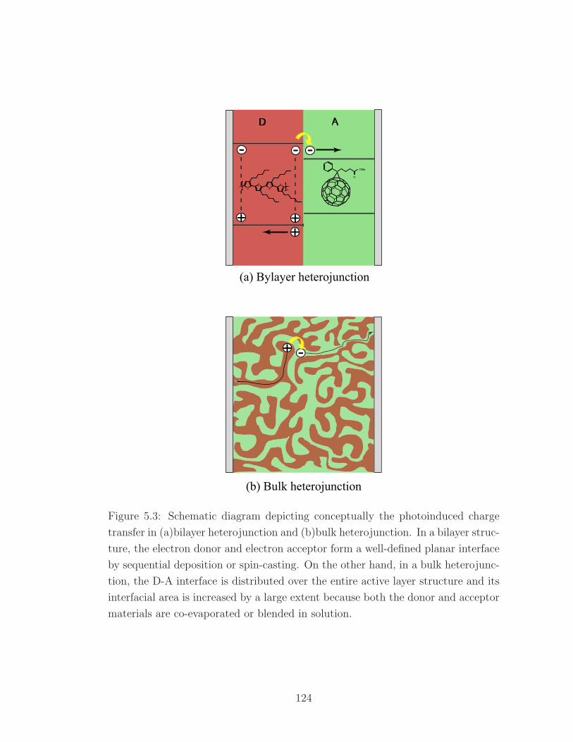
-+
+
-
+
- -
+
OMe
O
S
S
S
S* *n
(a) Bylayer heterojunction
(b) Bulk heterojunction
Figure 5.3: Schematic diagram depicting conceptually the photoinduced charge
transfer in (a)bilayer heterojunction and (b)bulk heterojunction. In a bilayer struc-
ture, the electron donor and electron acceptor form a well-defined planar interface
by sequential deposition or spin-casting. On the other hand, in a bulk heterojunc-
tion, the D-A interface is distributed over the entire active layer structure and its
interfacial area is increased by a large extent because both the donor and acceptor
materials are co-evaporated or blended in solution.
124

Therefore, we can write the external quantum efficiency ηEQE, which describes the
ratio of the number of free charge carriers to the number of incident photons
ηEQE =Iph/e
Plight/(hν)
=Nex
Nph
· NDAex
Nex
· NDAfree
NDAex
· NA,Cfree
NDAfree
= ηA · ηED · ηCT · ηCC
= ηA · ηIQE, (5.1)
where ηIQE = ηED · ηCT · ηCC is the internal quantum efficiency (IQE).
In this chapter, we will focus on the bulk heterojunction structure to develop
a photodetector with a high EQE. Although there are a number of different or-
ganic materials used in photovoltaic applications, including organic dyes or pig-
ments, the most commonly used active materials are, for hole conducting donor
materials, MDMO-PPV (poly[2-methoxy-5-(3,7-dimethyloctyloxy)]-1,4-phenylene-
vinylene), MEH-PPV (poly(2-methoxy-5-(2′-ethylhexyloxy)-1,4-phenylenevinylene)),
P3HT (poly(3-hexylthiophene-2,5-diyl)), P3OT (poly(3-octylthiophene)), PFB (poly-
(9,9′-dioctylfluorene-co-bis-N,N ′-(4-butylphenyl)-bis-N,N ′- phenyl-1,4-phenylen di-
amine), and pentacene, and for electron conducting acceptor materials, CN-PPV
(poly(2,5,2′,5′-tetrahexyloxy-7,8′-dicyano-di-p-phenylenevinylene), CN-MEH-PPV
(poly[2-methoxy-5-(2′-ethylhexyloxy)-1,4-(1-cyanovinylene)-phenylene), F8TB (poly-
(9,9′- dioctylfluoreneco-benzothiadiazole), fullerene C60 and C70, and chemically
modified soluble fullerene derivatives, namely PCBM-C60 ([6,6]-phenyl-C61-butyric
acid methyl ester) and PCBM-C70 ([6,6]-phenyl-C71-butyric acid methyl ester).
125

The materials used in this work are conjugated polymers, MEH-PPV and P3HT
for electron donors, and small organic molecules, PCBM-C60 and PCBM-C70 for
electron acceptor materials. Fig. 5.4 shows the chemical structures of these four
materials.
5.2 Fabrication of bulk heterojunction PDs
The device structure is shown in Fig. 5.5. Indium-tin-oxide (ITO) on float glass
substrate was purchased from Delta Technologies. The transparent conducting
oxide, ITO, with a sheet resistance of 4−8 Ω/ and a thickness of 200 nm was used
as the hole injecting electrode. In order to etch parts of the ITO to define several
devices on a 1′′ × 1′′ ITO/glass substrate, a photoresist pattern was transferred
onto the ITO layer by wet chemical etching using diluted HCl2. The etch rate can
be adjusted by varying the concentration of HCl. The typical etch rate is about
50 A/min in HCl aqueous solution (1:1, standard 38% HCl to DI water) at room
temperature and can be accelerated up to 2000 A/min in undiluted HCl (38%).
A digital voltmeter was used to check whether the ITO was completely cleared
without leaving any unwanted residual layer that can short out the device.
Once the patterned ITO/glass substrate was prepared, all the subsequent layers
were deposited in an inert N2 environment in a glove box to avoid photo-oxidative
degradation. After solvent cleaning of the ITO/glass substrate, a thin layer (∼
2ITO can be easily removed in HF as well. However, the etch rate is very high and often
uncontrollable, and, more importantly, it attacks the glass substrate at the same time. Reactive
ion etching in an Ar plasma is an alternative way to etch ITO when the feature size is small.
126

O
MeO
CH3
CH3
CH3
CH3
n
S
S
S
S* *n
(a) MEH-PPV
(b) P3HT
(c) PCBM-C60 (d) PCBM-C
70
OMe
O
OMe
O
Figure 5.4: The chemical structure of the materials in bulk heterojunction layer for
organic photodetector. (a) and (b) are electron donor/hole conducting conjugated
polymers, MEH-PPV and P3HT, respectively. (c) and (d) are electron accep-
tor/electron conducting small molecules, PCBM-C60 and PCBM-C70, respectively.
127

Glass substrate
ITO
PEDOT:PSS
Active layer
Al LiF
Figure 5.5: Schematic diagram of the device configuration.
50 nm) of PEDOT:PSS (poly[3,4-ethylenedioxythiophene]:poly[styrenesulfonate],
LED grade PEDOT Al4083 purchased from Baytron) was spin-coated and followed
by annealing at 150 C for 1 hr. Either ITO or PEDOT:PSS alone can be used
as the hole injecting anode, but the ITO/PEDOT:PSS combination employed in
OLEDs and OPV cells has given the most promising results for device efficiency
as well as lifetime [108–110].
A polymer/fullerene blend was spin-casted and annealed at 100 C for 1 hr for
the active layer with a desired thickness. The materials for the blend are conjugated
polymers MEH-PPV and P3HT for electron donors, and small organic molecules
PCBM-C60 and PCBM-C70 for electron acceptor materials, all of which were pur-
chased from American Dye Source. Chlorobenzene was used to dissolve both of
these organic materials for a solution process because chlorobenzene can provide
more uniform mixing of the constituents compared with other organic solvents
128
such as toluene, which is also frequently used. This more uniform mixing mainly
comes from the higher solubility of C60, and results in a smooth surface morphol-
ogy and hence an improved photocurrent [111]. Separate solutions of polymer and
fullerene were prepared and stirred at 80 C for a few days and then filtered into a
pre-cleaned vial to prepare a blend solution with a desired relative concentration
of donor/acceptor. The total solution concentration in weight was kept about 1%
for a layer with a thickness about 100 nm.
As mentioned earlier, the nanoscale morphology of the active layer in a bulk-
heterojunction is an important factor because the presence of an intimate inter-
penetrating network between the electron donor and acceptor materials is critical
for efficient charge transport. For this reason, a detailed study was conducted
earlier in our group (R. Barber, W. Herman, and D. Romero) to investigate how
the morphology and device characteristics depend on the relative concentration of
the active layer blend [112,113].
Figure 5.6 shows the atomic force microscopy (AFM) images for four different
PCBM-C60 molar fractions in the blend with a block copolymer MEH-PPV-co-
biphenylene vinylene [113]. The molar fraction of PCBM-C60 x is defined as
x =WC60
/MWC60
WC60/MWC60
+ Wpoly/MWpoly
. (5.2)
Therefore, x = 1 denotes pure C60, x = 0 denotes pure MEH-PPV polymer, and
x = 0.5 corresponds to the blend containing one C60 molecule for every repeat-
ing unit of the polymer. The AFM images of different surface morphologies with
129

5 µm 5 µm
5 µm 5 µm
c) x=0.26 d) x=0
a) x=1 b) x=0.43
Figure 5.6: Atomic Force Microscopy (AFM) images for four different PCBM-C60
molar fractions x [113].
130

varying fullerene concentrations clearly show that smooth morphology with uni-
form fine grains (∼ 100 nm), rather than segregated large clusters (∼ 1 µm) can
be achieved at intermediate values of x.
Further study on photovoltaic device characteristics depending on fullerene
concentration showed that when the molar fraction of C60 in the MEH-PPV
copolymer/C60 blend is around 0.6 (or equivalently, 3:1 in weight for this par-
ticular example), the device exhibits the best performance in terms of short circuit
current, fill factor, EQE, and PCE [113]. Note that the optimized relative ratio can
be significantly different when other materials are used. For instance in P3HT/C60
blend, the optimized ratio is close to x = 0.17 (or equivalently, 1.1:1 in weight for
this particular example).
For an electron-injecting top contact, a ∼ 1 nm thick layer of lithium-fluoride
(LiF) followed by a ∼ 60 nm thick layer of aluminum (Al) was deposited on top
of the organic layer via shadow mask technique using a thermal evaporator inside
the glove box. Similar to the case of the ITO/PEDOT:PSS combination that was
used for the hole-injecting electrode for the purpose of energy barrier engineering,
a very thin layer of LiF was inserted between the active layer and the Al cathode
in order to enhance the electron injection efficiency [114,115].
5.3 Device characteristics
Characterization of the devices was performed under an AM 1.5 solar simulator
with an intensity of 92 mW/cm2 and/or using a CW laser at a wavelength of 532 nm
131

with a maximum output power of 5 W.
A practical figure of merit for PV cells is the PCE (ηP), which is defined as the
ratio of the maximum electrical power generated to the incident light power [116],
ηP =maxI · V
Plight
=ISC · VOC
Plight
FF, (5.3)
where maxI · V is the maximum electrical power that the device can deliver to
an external load, Plight is the incident light power, ISC is the short-circuit current
(current at zero voltage), VOC is the open-circuit voltage (voltage intercept at zero
current), and FF is the fill factor defined as
FF =maxI · V ISC · VOC
, (5.4)
The PCE can also be expressed with the EQE (ηEQE) and the energy conversion
efficiency (ξen) at a particular wavelength as
ηP = ηEQE · ξen · FF, (5.5)
with
ηEQE =Iph/e
Plight/(hν), (5.6)
ξen =eVOC
hν. (5.7)
Note, however, that Eqs. 5.5–5.7 are more useful for describing the detector re-
sponse at a particular wavelength because PV cell are characterized under AM
132

-1.0 -0.5 0.0 0.5 1.0-8
-4
0
4
8
JS
C
(m
A/c
m-2 )
Bias voltage (V)
dark
AM 1.5
Figure 5.7: Current versus voltage (I-V ) characteristics of the bulk heterojunction
device of MEH-PPV copolymer and PCBM-C60 with a C60 molar fraction x = 0.57.
VOC = 0.88 V, JSC = 4.92 mA/cm2, FF = 0.47, and ηP = 2.4% under AM1.5 direct
solar simulator with Pin = 92 mW/cm2 [113].
1.5 solar illumination in most cases. The incident photon to current conversion
efficiency (IPCE),
IPCE[%] =1240 · ISC[µA]
λ[nm] · Plight[W ](5.8)
is often used instead of EQE (ηEQE), but they are equivalent to each other.
Figure 5.7 shows the current versus voltage (I-V ) characteristics in the dark and
under solar illumination for the bulk heterojunction device of MEH-PPV copoly-
mer and PCBM-C60 with a C60 molar fraction x = 0.57. We can extract the PV
133

characteristics of the device, VOC = 0.88 V, JSC = 4.92 mA/cm2, FF = 0.47, and
ηP = 2.4% under AM 1.5 direct solar simulator with Pin = 92 mW/cm2.
A practical figure of merit for PDs is the EQE or photo-responsivity at a certain
wavelength, while it is the PCE for the PV cells. In order to describe an overall
detector performance, a high EQE alone is not sufficient and other parameters
such as dark current, noise equivalent power, dynamic range, and response time,
should be considered as well. However, a high EQE is a prerequisite. Although a
detector can be used in ‘PV mode’, operating without any bias voltage applied,
most detectors operate under reverse bias voltage for fast carrier sweep within the
active layer. Therefore, depending on whether the device is employed as a solar
cell or a detector, a slightly different approach is needed. Our primary interest in
the rest of this chapter is to improve the EQE at the wavelengths of peak detector
responsivity by increasing the photocurrent under reverse bias.
Figure 5.9 shows the I-V characteristics of the bulk heterojunction detector of
P3HT/PCBM-C60 with a relative ratio, C60/P3HT = 1.15 in weight, (a) under AM
1.5 solar illumination and (b) under different laser intensities at 532 nm. As shown
in Fig. 5.8, the absorption peak of the blend of P3HT/PCBM-C60 is near 532 nm,
and hence the maximum detector responsivity is expected at around 532 nm as
well. Although the PCE under solar illumination is poor ηP < 0.5% mainly due to
the small fill factor FF ≈ 0.2, the EQE is around 0.3 at short circuit condition and
approaches 0.6 at V = −10 V as shown in the figure. These lower PCE but higher
EQE, in comparison with the previous device from MEH-PPV/C60 (ηp = 2.4 %
134

400 600 800 1000 12000.0
0.2
0.4
0.6
0.8
1.0
Absorb
ance
Wavelength (nm)
Figure 5.8: Absorption spectra of the blend of P3HT/PCBM-C60. The absorption
peak of the blend of P3HT/PCBM-C60 is near 532 nm.
and ηEQE < 0.1) reported in the earlier work [113], clearly indicate that an efficient
PV cell with a high PCE is not necessarily an efficient detector requiring a high
EQE and a slightly different approach is needed depends on whether the device is
employed as a solar cell or a detector. The value of EQE achieved (ηEQE = 0.3
and 0.6 at V = 0 V and −10 V, respectively) is reasonably high, but in order to
improve it further, we need to estimate how many photons arrive and are absorbed
within the active layer by taking into account of multilayer thin film interference
effects.
135

10 8 6 4 2 0 27
6
5
4
3
2
1
0
1
2
Bias voltage (V)
Photo
curr
ent densi
ty (
mA
/cm
2)
(a) under solar AM 1.5 illumination
10 8 6 4 2 0 22
1. 5
1
0. 5
0
0.5
1
Bias voltage (V)
Photo
curr
ent densi
ty (
mA
/cm
2)
(b) under laser (@ 532 nm) illumination
Figure 5.9: I-V characteristics of the bulk heterojunction device of P3HT and
PCBM-C60 with a C60/P3HT 1.1 in weight, (a) under AM 1.5 direct solar illumi-
nation (b) under different laser intensities at 532 nm.
136

-10 -8 -6 -4 -2 00
0.2
0.4
0.6
0.8
1
Bias volatge (V)
Ext
ern
al q
uantu
m e
ffic
iency
,
η
EX
E
P=2.06 mW/cm2
P=3.13 mW/cm2
P=4.92 mW/cm2
P=5.78 mW/cm2
P=6.95 mW/cm2
Figure 5.10: External quantum efficiency vs. bias voltage of the device from P3HT
and PCBM-C60 at 532 nm. ηEQE is around 0.3 at short circuit condition and
approaches 0.6 at V = −10 V.
137
5.4 Multilayer thin film interference effects
Because the number of excitons generated is directly related to the absorption of
optical energy, in order to improve the external quantum efficiency, the first step
to consider is maximizing the number of photons that arrive in the active layer,
where photoexcited excitons are generated and dissociated into free carriers.
Because the exciton diffusion and dissociation efficiencies are near 100% in the
bulk heterojunction as mentioned in section 5.1, we can define a theoretical upper
limit of EQE that assumes all the free carriers from the dissociated excitons are
collected at the respective electrodes (ηCC = 1). We expect that this upper limit of
EQE can be nearly achieved when the detector is under a relatively strong reverse
bias.
For the estimation of EQE, a model including interference effects from multiple
reflection and transmission at each interface is necessary to calculate the optical
field distribution in each layer. This interference effect is particularly important
when there is a very strong reflection at the conducting electrode and polymer
interface as the case of our device. When considering a device model of a stratified
structure, knowledge of the complex refractive indices and thicknesses of all the
layers is a prerequisite.
5.4.1 Optical properties of individual layers
For the numerical modeling to calculate the optical field profile in the stratified
structure, the complex refractive indices and thicknesses of individual layers were
138

determined by a spectroscopic ellipsometry (J.A. Wollam) employing a model fit-
ting procedure using the Drude-Lorentz model [117, 118]. The complex dielectric
function ǫ(ω) in the Drude-Lorentz model can be expressed as
ǫ(ω) = ǫR − jǫI (5.9)
= ǫ∞ +f0ω
2p
−ω2 + jωΓ0
+n
∑
k=1
fkω2p
(ω2k − ω2) + jωΓk
, . (5.10)
where ωp is the plasma frequency and n is the number of Lorentz oscillators with
a center frequency of ωk, a strength of fk and a damping constant Γk. This Drude-
Lorentz model combines the free-electron model to represent intraband optical
transition and the bound-electron model for interband effects. In general, there
can be one or more Lorentz oscillators depending on the material. The complex
index of refraction n can be determined from the complex dielectric function:
n =√
ǫ = n − jk. (5.11)
Figure 5.11 (a) shows the measurement result for the real and imaginary index
of refraction of the ITO on soda lime glass substrate. For the model fit to extract n
and k from ellipsometric data, one Lorentz oscillator in the Drude-Lorentz model
(n = 1 in Eq. 5.10) was enough to achieve an excellent fit in the case of ITO [119].
Also note that the thickness obtained from a profilometer was used for an initial
guess value in the fitting procedure.
In order to validate the measurement of the complex refractive index, the values
of n and k, and the thickness from the best-fit model for the ellipsometric data
139

were used to generate the transmission data, and the generated transmission curve
was compared with the experimentally measured UV/Vis/IR transmission from a
spectrophotometer as shown in Fig. 5.11 (b).
With the same procedure as ITO, the optical properties and thicknesses of other
layers were also determined. Figure 5.12 shows the n and k for Al, PEDOT:PSS,
and P3HT:C60. The optical properties of LiF were not shown in the figure because
the index dispersion of LiF is very flat, ∼ 1.39, in both the visible and near-IR
region, and absorption in a 1 nm thick LiF layer is negligible.
5.4.2 Effect of multilayer thin film interference
Once all the optical properties and thicknesses of individual layers were determined
as discussed in the previous section, we can calculate the optical field distribution
and absorption of light in each layer of the stratified device structure. Although
there are a few different ways to perform the calculation, we follow the approach
of the work reported in [91, 101]. In this model, we assume a plane wave incident
normal to the device, homogeneous and isotropic layers, and parallel and smooth
interfaces.
To calculate the optical electric field as a function of position within the device,
consider the schematic diagram of the multilayer structure of the device as shown
in Fig. 5.13. The field in the i-th layer has two components, E+i and E−
i , propa-
gating in the positive and the negative z direction, respectively. In this case, the
electric field of the light can be represented by a 2 × 2 matrix because equations
140

300 500 700 900 1100 1300 15000
0.5
1
1.5
2
2.5
Wavelength (nm)
n
300 500 700 900 1100 1300 15000
0.5
1
1.5
2
2.5
k
n
k
(a) n and k of ITO film
400 600 800 1000 1200 14000
0.1
0.2
0.3
0.4
0.5
0.6
0.7
0.8
0.9
1
Wavelength (nm)
Tra
nsm
issi
on
modelUV/Vis/IR
Substrate
R
T
Film
(b) Transmission of ITO/glass sample
Figure 5.11: (a) Real and imaginary index of refraction measured from the spec-
troscopic ellipsometric data and model fit with the Drude-Lorentz model. (b)
Comparison between the estimated transmission using the n and k, and thickness
from the best-fit model and the measured transmission from a spectrophotometer.
141

300 400 500 600 700 800 900 10000
0.5
1
1.5
2
2.5
3
Wavelength (nm)
n
AlPEDOTP3HT:C
60
(a)
300 400 500 600 700 800 900 10000
1
2
3
4
5
6
7
8
9
10
Wavelength (nm)
k
AlPEDOTP3HT:C
60
(b)
Figure 5.12: Optical properties of Al, PEDOT:PSS, and P3HT:C60
142

Glass Substrate ITO PEDOT:PSS
Active layer
AlLiF
Rs
TsR
T
RD
TD
d0=1 mm d1=200 nm d2=50 nm d3=dA d4=1 nm d5=60 nm
E0+ E1
+ E2+ E3
+ E4+ E5
+ E6+
E0- E1
- E2- E3
- E4- E5
- E6-
xz
y
Figure 5.13: Schematic diagram of the multilayer device structure with the thick-
nesses and the optical electric fields in each layer, E+i and E−
i , representing the
component propagating in the positive and the negative z direction, respectively.
describing the light propagation are linear, and the tangential components of the
field are continuous across the interface. In this particular example, five thin film
layers are stacked to form the actual device. A 1 mm thick glass substrate was
not directly included in the thin-film analysis because the light travelling within
the glass substrate could be treated as effectively incoherent light by considering
the average effect combining the angular dispersion of incident light, the finite
bandwidth of the light source, and the surface roughness and nonuniformity in the
thickness of the substrate. The substrate effect can be incorporated by considering
the reflectivity RD and transmissivity TD of the entire device after we calculate R
143

and T of the multilayer structure, i.e.
RD =RS + R − 2RSR
1 − RSR, (5.12)
TD =TST
1 − RSR, (5.13)
AD = 1 − RD − TD, (5.14)
with
RS =
∣
∣
∣
∣
1 − n0
1 + n0
∣
∣
∣
∣
2
, (5.15)
TS = n0
∣
∣
∣
∣
2
1 + n0
∣
∣
∣
∣
2
, (5.16)
where RS and TS are respectively the reflectivity and transmissivity at the air/glass
interface, AD is the total absorption in the device, and n0 is the complex refractive
index of the glass substrate.
To calculate the optical fields as a function of position in the most general case,
consider m layers and corresponding fields Ei (i = 0 ...m + 1). Then we can write
an expression that relates the two outermost fields E0 and Em+1,
E+0
E−0
= S ·
E+m+1
E−m+1
, (5.17)
with the scattering matrix S defined as
S =
S11 S12
S21 S22
=
m∏
p=1
I(p−1)pLp
· Im(m+1), (5.18)
144

where Iij is the interface matrix representing the reflection and transmission at the
i-j interface and Li is the layer matrix representing a phase change through the
i-th layer as defined below.
Li =
ejk0nidi 0
0 e−jk0nidi
, (5.19)
Iij =
1tij
rij
tij
rij
tij
1tij
, (5.20)
rij =ni − nj
ni + nj
, (5.21)
tij =2ni
ni + nj
, (5.22)
where ni = ni − jki is the complex refractive index and di is the thickness of the
i-th layer. Note that the complex Fresnel reflection coefficient rij and transmission
coefficient tij are the same for TE and TM modes when the light is incident normal
to the surface.
When light is incident on the glass and travels through the device in the +x
direction and E−m+1 = 0, we can obtain the complex coefficients r and t.
r =E−
0
E+0
=S21
S11
, (5.23)
t =E+
m+1
E+0
=1
S11
, (5.24)
Therefore, the reflectivity R and transmissivity T described in Fig. 5.13 can be
145

written as
R = |r|2, (5.25)
T =|t|2n0
. (5.26)
To obtain the electric field within the i-th layer, the total multilayer transfer
matrix can be divided into two subsets, SLi and SR
i . Hence, we can write an
expression
S = SLi LiS
Ri , (5.27)
with
SLi =
i−1∏
p=1
I(p−1)pLp
· I(i−1)i, (5.28)
SRi =
m∏
p=i+1
I(p−1)pLp
· Im(m+1). (5.29)
From the equations above, we can obtain the electric field propagating in the +x
direction in the i-th layer with respect to the incident optical field,
E+i = t+i E+
0 =
1S−
i11
1 +S−
i12S+
i21
S−
i11S+
i11
e−j2k0nidi
E+0 , (5.30)
Similarly the electric field propagating in the −x direction in the i-th layer with
respect to the incident optical field is given by,
E−i = t−i E+
0 =
S+i21
S−
i11S+
i11
e−j2k0nidi
1 +S−
i12S+
i21
S−
i11S+
i11
e−j2k0nidi
E+0 . (5.31)
Therefore, the total electric field in the i-th layer at an arbitrary distance x to the
146

300 400 500 600 700 800 900 10000
0.1
0.2
0.3
0.4
0.5
0.6
0.7
0.8
0.9
1
X: 532Y: 0.8322
Wavelength (nm)
RD, A
D
X: 532Y: 0.1634
Absorption (1-RD -TD )
Reflection (RD)
Glass
Figure 5.14: Calculation of reflectivity RD and absorption AD = 1−RD−TD of the
device illustrated in Fig. 5.13 with a bulk heterojunction active layer P3HT/C60
with a thickness 100 nm.
right of the (i-1)/i interface can be written as
Ei(x) = E+i (x) + E−
i (x) (5.32)
= (t+i e−jk0nidi + t−i ejk0nidi)E+0 . (5.33)
Figure 5.14 depicts the calculated reflectivity RD and absorption AD = 1 −
RD − TD of the bulk heterojunction device from P3HT/C60 with a thickness of
100 nm. Interestingly, at a wavelength of 532 nm, about 16.3% of the total inci-
dent photons are reflected at the air/device interface and do not even reach the
active layer to generate excitons. This reflectivity is much higher than the 4%
147

50 100 150 200 250 300 350 4000
0.2
0.4
0.6
0.8
1
Distance from sub/ITO interface (nm)
|E(x
)|2
ITO AlPEDOT:PSSPEDOT:PSS LiFLiFP3HT/C60
Figure 5.15: Calculation of field distribution as a function of position. Modulus
squared of the optical electric field |E(x)|2 is normalized to the incident light field
|E+0 |2.
reflection at a simple air/glass interface, which might have been expected. This
calculation directly indicates how strongly the multilayer interference depends on
how we construct the practical device structure. It also clearly states that the
external quantum efficiency – the fraction of incident photons in the device that
can contribute to the photocurrent – can never exceed 83.2%, which is the total
light absorption in the entire device. In other words, if all the absorbed photons
could contribute to the photocurrent, an EQE of 83.2% would be obtained.
Figure 5.15 shows the calculated field distribution as a function of position. The
modulus squared of the optical electric field |E(x)|2 is normalized to the incident
148

light field |E+0 |2.
It is worth pointing out that a detailed field profile within the active layer
is very crucial in a bilayer structure because, in order to maximize the number
of excitons at the donor/acceptor interface, where the excitons dissociate most
efficiently into free carriers, a global peak of |E(x)|2 needs to be located near the
interface [101]. However, this is not the primary factor determining the EQE in
the bulk heterojunction device.
Once the optical field profile is found, we can calculate the time-averaged ab-
sorbed power or the number of absorbed photons as a function of position, which
is directly proportional to the number of excitons generated.
Qi(x) = αiIi(x)
=1
2cǫ0niαi|Ei(x)|2
=2πcǫ0niki
λ|Ei(x)|2, (5.34)
where αi is the absorption coefficient, and Ii(x) is the light intensity in the i-th
layer.
Figure 5.16 plots the calculated absorbed power Q(x) as a function of position.
Note that the simple exponential model Q(x) = αI0 exp (−αx), neglecting multiple
reflections and transmissions at the interfaces between the layers, can only give an
approximate exciton generation profile [120,121]. The total absorbed light within
the active layer only is given by
IAabs =
∫
dA
QA(x) dx, (5.35)
149

50 100 150 200 250 300 350 4000
0.2
0.4
0.6
0.8
1
1.2
1.4
1.6
1.8
2x 10
4
Distance from sub/ITO interface (nm)
Q(x
)
ITO AlPEDOT:PSSPEDOT:PSS LiFLiFP3HT/C60
Figure 5.16: Calculation of time-averaged absorbed power Q(x) as a function of
position.
and we can define the upper limit to the external quantum efficiency ηLEQE as
ηLEQE =
IAabs
Iinc
, (5.36)
where Iinc is the intensity of the incident light. This ηLEQE represents the theoretical
upper limit of EQE that can be achieved from a specific device structure once all
the optical properties and thicknesses of individual layers are measured. In other
words, we can achieve ηLEQE, the maximum incident photons to current conversion
efficiency, when all the photons absorbed in the active layer contribute to the
photocurrent. This is equivalent to assuming that the internal quantum efficiency
ηIQE is unity, i.e. the exciton diffusion ηED, exciton dissociation ηCT, and charge
150

collection efficiency ηCC in Eq. 5.6 are 100%.
It should be noted that, for a comprehensive theoretical estimation of the EQE,
we need to solve the one-dimensional steady-state carrier transport equation and
current density equation [122,123].
Dd2
dx2n(x) + µE
d
dxn(x) − n(x)
τ+
γQ(x)
hν= 0 (5.37)
J(x) = qµEn(x) + qDd
dxn(x) (5.38)
where D is the diffusion constant, µ is the charge mobility, E is electric field, n(x)
is the carrier density, τ is the carrier life-time, and γ is the carrier generation rate,
which is equivalent to ηED ·ηCT. However, it is not straightforward to solve this car-
rier transport equation numerically, mainly because it is a multi-point boundary
value problem requiring all the boundary conditions at the interfaces. In addi-
tion, the field-dependence of the charge mobility cannot be neglected under strong
electric fields associated with the applied reverse bias. Therefore determining the
charge mobility becomes very crucial in the calculation.
Nevertheless, the ηLEQE is still a very useful quantity for the photodetector under
applied fields E ≫ 106V/m because, under such strong fields, ηCC can easily reach
80–90%, and this leads to a value of EQE about 80–90% of ηLEQE.
The calculated ηLEQE for the device structure above is 0.69. Therefore, the EQE
we obtained (ηEQE = 0.6 at −10 V as shown in Fig. 5.10) is 87% of ηLEQE, leading
to ηCC = 0.87.
151

5.5 Improvement of the external quantum efficiency
So far, we used PEDOT:PSS and LiF together with ITO and Al, respectively, to
form electrodes for more efficient hole and electron injection. This is a desirable
approach to achieve high short-circuit currents and high PCE in PV cells by com-
pensating energy level offset or band bending at non-ideal ohmic contacts. In the
detector, however, the carriers are expected to have enough energy to overcome
these energy level misalignments under a strong applied reverse bias. In addition,
the PEDOT:PSS layer absorbs a non-negligible amount of photons and reduces
the number of photons absorbed within the active layer.
Figure 5.17 shows the calculated field profile |E|2 and time-averaged absorbed
power Q as a function of position in the case where there is no PEDOT:PSS and
LiF. As we might have expected, the upper limit of the external quantum effi-
ciency ηLEQE increases to 87.8% from 69% in the previous case of glass/ ITO/ PE-
DOT:PSS/ P3HT:C60/ LiF/ Al.
In order to study the active layer thickness dA dependence on ηEQE, we fabri-
cated devices with three different thicknesses shown in Fig. 5.18 with a structure
of glass/ITO/P3HT:C60/Al. Figure 5.19 plots the calculation of ηLEQE with (dotted
line) and without PEDOT:PSS and LiF (solid line) and measured EQE at -10 V
(triangles). Interestingly, when PEDOT:PSS and LiF are used, the EQE has a
global peak value of 0.69 at a thickness of 100 nm and has a local minimum of 0.60
at a thickness of about 170 nm, which can be explained by multilayer interference
152

50 100 150 200 250 300 3500
0.2
0.4
0.6
0.8
1
Distance from sub/ITO interface (nm)
|E(x
)|2
ITO AlP3HT/C60
(a)
50 100 150 200 250 300 3500
0.2
0.4
0.6
0.8
1
1.2
1.4
1.6
1.8
2x 10
4
Distance from sub/ITO interface (nm)
Q(x
)
ITO AlP3HT/C60
(b)
Figure 5.17: Calculation of field distribution |E(x)|2 and time-averaged ab-
sorbed power Q(x) as a function of position for the device structure of
glass/ITO/P3HT:C60/Al.
153
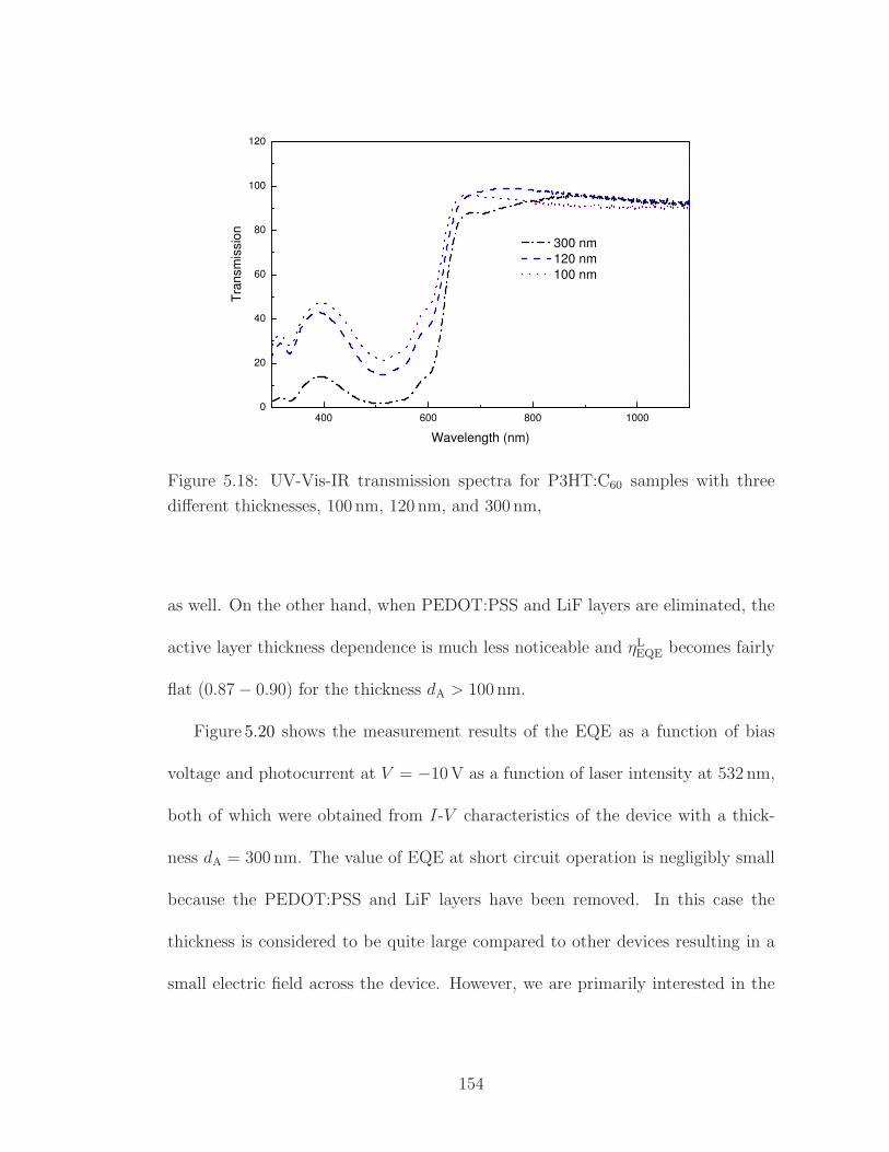
400 600 800 10000
20
40
60
80
100
120
300 nm
120 nm
100 nm
Tra
nsm
issio
n
Wavelength (nm)
Figure 5.18: UV-Vis-IR transmission spectra for P3HT:C60 samples with three
different thicknesses, 100 nm, 120 nm, and 300 nm,
as well. On the other hand, when PEDOT:PSS and LiF layers are eliminated, the
active layer thickness dependence is much less noticeable and ηLEQE becomes fairly
flat (0.87 − 0.90) for the thickness dA > 100 nm.
Figure 5.20 shows the measurement results of the EQE as a function of bias
voltage and photocurrent at V = −10 V as a function of laser intensity at 532 nm,
both of which were obtained from I-V characteristics of the device with a thick-
ness dA = 300 nm. The value of EQE at short circuit operation is negligibly small
because the PEDOT:PSS and LiF layers have been removed. In this case the
thickness is considered to be quite large compared to other devices resulting in a
small electric field across the device. However, we are primarily interested in the
154
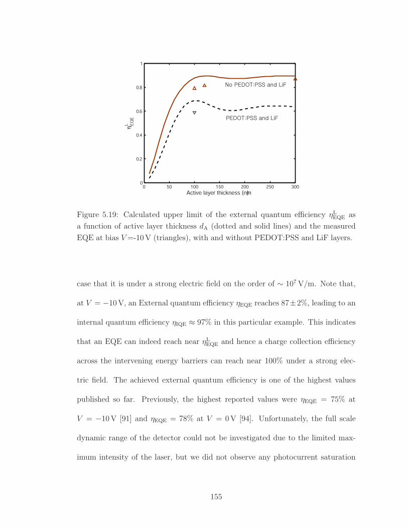
0 50 100 150 200 250 3000
0.2
0.4
0.6
0.8
1
Active layer thickness (nm)
ηE
QE
L
Figure 5.19: Calculated upper limit of the external quantum efficiency ηLEQE as
a function of active layer thickness dA (dotted and solid lines) and the measured
EQE at bias V =-10 V (triangles), with and without PEDOT:PSS and LiF layers.
case that it is under a strong electric field on the order of ∼ 107 V/m. Note that,
at V = −10 V, an External quantum efficiency ηEQE reaches 87±2%, leading to an
internal quantum efficiency ηIQE ≈ 97% in this particular example. This indicates
that an EQE can indeed reach near ηLEQE and hence a charge collection efficiency
across the intervening energy barriers can reach near 100% under a strong elec-
tric field. The achieved external quantum efficiency is one of the highest values
published so far. Previously, the highest reported values were ηEQE = 75% at
V = −10 V [91] and ηEQE = 78% at V = 0 V [94]. Unfortunately, the full scale
dynamic range of the detector could not be investigated due to the limited max-
imum intensity of the laser, but we did not observe any photocurrent saturation
155

up to an intensity of IL = 70 mW/cm2.
5.6 Summary
In this chapter, we investigated the highly efficient organic thin film bulk hetero-
junction photodetector fabricated from a blend of conjugated polymer (P3HT) and
small molecule (fullerene C60). We have benefited from the ideas developed in the
study of OPV cells because the OPD shares fundamental photophysics with the
OPV cell in terms of the photocurrent generation process. However, the detec-
tor needs a slightly different approach from that used in a photovoltaic cell. We
addressed the effect of multilayer thin film interference on the external quantum
efficiency. From the numerical modeling to calculate the optical field distribu-
tion and absorption of light energy in the layers, based on the characterization
of optical properties of individual layers comprising the detector, we proposed a
bulk heterojunction photodetector without PEDOT:PSS and LiF layers that are
commonly used in photovoltaic cells for high short-circuit current. Through the
experimental I-V characterization using a CW laser at a wavelength of 532 nm, we
demonstrated that it exhibited an external quantum efficiency ηEQE = 87±2% un-
der an applied bias voltage V = −10 V, leading to an internal quantum efficiency
ηIQE ≈ 97%. These results show that the charge collection efficiency across the in-
tervening energy barriers can indeed reach near 100% under a strong electric field.
The achieved external quantum efficiency is one of the highest values published so
far.
156

-10 -8 -6 -4 -2 00
0.2
0.4
0.6
0.8
1
Bias Volatge (V)
ηE
XT
(a)
0 10 20 30 40 50 60 700
0.1
0.2
0.3
0.4
0.5
Laser Intensity (mW/cm2)
Ph
oto
curr
ent
(mA
)
(b)
Figure 5.20: Measured ηEQE as a function of applied reverse bias voltage (a) and
photocurrent at V = −10 V as a function of incident laser intensity (b) for a device
with a dA = 300 nm.
157

Chapter 6
Conclusions
6.1 Summary and accomplishments
This dissertation work was motivated by emerging interests in investigating the
technological feasibilities of novel photonic and optoelectronic components fab-
ricated from new classes of organic materials. Due to this nature, the research
work was truly a multi-disciplinary subject and has been carried out with a strong
collaboration with chemists and physicists. The subject was grouped into three
principal parts describing different types of devices that are somewhat independent
of each other, but can be integrated into single devices; optical chiral waveguides
and magneto-optic materials, waveguides and microring devices from perfluori-
nated polymer, and organic bulk heterojunction photodetectors from conjugated
polymer and fullerene.
First, we studied unique polarization properties of novel organic chiral mate-
rials and optical chiral waveguides fabricated from binaphthyl-based chiral single
molecular compounds that can be formed into glassy isotropic thin solid films with
negligible birefringence. Asymmetric chiral-core planar waveguides were evaluated
for viable applications including an integrated-optic polarization rotator. Through
158
a detailed experimental polarization analysis on the waveguide eigenmodes, we
showed that the eigenmodes of the waveguides were indeed elliptically polarized
modes with the mode ellipticities on the order of 0.25, which agrees well with the
one predicted in the recent theory. The mode ellipticity that we obtained was not
large enough to meet the requirement for practical devices such as a polarization
rotator – predominant circularly polarized modes – but, to the best of our knowl-
edge, it was the first experimental demonstration of the mode ellipticities of the
chiral-core optical waveguides.
We also characterized novel organic magneto-optic materials, which can be vi-
able alternatives to the chiral materials. Measurement of the Verdet constants from
organic thin-film samples (10 − 100 µm) under a moderate magnetic field can be
very challenging and requires a very sensitive measurement technique. We adopted
a homodyne balanced detection with a sensitivity that can determine an angle of
polarization rotation as small as 0.5 × 10⁻⁶ radian and successfully measured the
Verdet constants of organic samples provided by Georgia Tech at different wave-
lengths. We measured Verdet constants of 10.4 and 4.2 rad/T · m at 1300 nm and
1550 nm, respectively, from an organic sample provided by Georgia Tech, which is
comparable to that of terbium gallium garnet. This unique observation can lead to
a new opportunity to build integrated-optic isolators or circulators from a simple
fabrication methodology including spin-casting and photolithography.
Second, we investigated low-loss waveguides and microring resonators fabri-
cated from perfluorocyclobutyl (PFCB) copolymer, which has substantially low
159

material absorption loss at telecommunication wavelengths. We discussed the de-
sign, fabrication, and characterization of those devices. We provided practical
design parameters through a waveguide eigenmode analysis, 3-D full vectorial cal-
culation for bending loss estimation, and the coupled mode theory for an estimation
of a coupling efficiency. A couple of fabrication challenges, an adhesion and mask
cracking problems, were also addressed. From the experimental characterization,
we demonstrated the two different types of straight waveguides, a buried channel
and pedestal structures, with propagation losses of 0.3 dB/cm and 1.1 dB/cm, re-
spectively. A microring add-drop filter with a maximum extinction ratio of 4.87 dB,
quality factor Q = 8554, and finesse F = 55 was also demonstrated. In addition,
we showed experimentally that all-optical switching with the PFCB microring res-
onator is possible when it is optically pumped with a femtosecond laser pulse of
sufficient energy. For a microring-loaded Mach-Zehnder interferometer (MR-MZI),
we demonstrated a modulation window of 30 ps and a maximum modulation depth
of 3.8 dB from an optical pump with a pulse duration of 100 fs and a pulse energy of
500 pJ when the signal wavelength is initially tuned to one of the ring resonances.
Finally, we investigated the highly efficient organic bulk heterojunction pho-
todetector fabricated from a blend of conjugated polymer and small molecule,
P3HT/PCBM-C60. For a numerical modelling accounting for multilayer interfer-
ence effects on the external quantum efficiency of a detector, the optical properties
and thicknesses of all the individual layers constituting the device were character-
ized by the spectroscopic ellipsometry and thin film transmission measurement.
160

Based on the numerical result, we proposed a bulk heterojunction photodetector
without containing PEDOT:PSS and LiF layers that are widely used for efficient
charge injection in a photovoltaic cell. Experimental I-V characterization at a
wavelength of 532 nm exhibited that the external quantum efficiency ηEQE could
reach near the theoretical upper limit efficiency ηLEQE under a strong electric field.
From a P3HT/C60 bulk heterojunction device, we achieved a very high external
quantum efficiency ηEQE = 87 ± 2% leading to an internal quantum efficiency
ηIQE ≈ 97% under an applied bias voltage V = −10 V. These results show that the
charge collection efficiency across the intervening energy barriers can indeed reach
near 100% under a strong electric field. The achieved external quantum efficiency
is one of the highest values obtained so far.
6.2 Future work
We have discussed the technological feasibility of photonic devices based on truly
novel organic materials. Therefore, by nature, the work discussed in this thesis
is still in progress in many aspects. Most of the materials that were used in this
dissertation work are not even commercially available and suffer from incomplete
understanding on their physical, optical and electronic properties. By the same
token, fabricating devices can be extremely challenging, and sometimes it can take
a very long time to develop a new process technique suitable for those materials.
Long term reliability is another problem that needs to be resolved for success-
ful commercialization. For these reason, a strong collaboration among engineers,
161

physicist, and chemist is required.
In order for chiral waveguides to be used as a TE/TM converter or a polar-
ization rotator, the eigenmodes must be predominantly circularly polarized states,
achievable by increased material chirality along with negligible birefringence. We
showed that, for a given material chirality, the mode ellipticity in a weekly guided
waveguide is much higher than a tightly confined waveguide. However, for nearly
circularly modes, a chirality at least an order magnitude larger (γ ≈ 4 pm or
equivalently, bulk ρ = 60 deg/mm) than the one we presented is required. It is
also desirable to extend the ORD maxima towards the telecommunication wave-
lengths for optical communication applications. Certain types of chiral compounds
are very sensitive to UV light and they tend to racemize in the air. Therefore, so-
lutions to this photoracemization need to be addressed as well in the future. It
should not be an easy task, but developing a numerical technique to analyze the
eigenmode and the mode ellipticity in 3D guiding structures can provide a very
useful tool for designing a practical integrated optic chiral devices.
The Verdet constants from organic materials we observed were moderate, but
this unique observation opens the possibility that integrated optic isolators or
circulators can easily be constructed from a simple fabrication methodology in-
cluding spin-casting and photolithography. However, in order to build practical
devices, much work needs to be done to synthesize the materials with even larger
Verdet constants, and to investigate the polarization properties of the eigenmodes
in magneto-optic waveguides. In addition, a comprehensive theoretical study in-
162

cluding a quantum mechanical approach is needed to understand the origin of the
large Verdet constants from organic materials.
More theoretical and experimental investigation is necessary for the PFCB-
based waveguide devices. Although we did not discuss the numerical techniques
to calculate the scattering loss, it can be done by modifying our finite difference
code properly to employ a radiative scattering source. Aside from achieving a
narrower gap, much needs to be done to refine the etch process in order to reduce
the scattering loss, which is a dominant source increasing the total loss in the
PFCB waveguides. A different etching condition in RIE, or different etching tools
including an inductive coupled plasma etching (ICP) can be tried. A post-etching
process such as chemical or thermal treatment may allow us to achieve much
smoother side wall. In addition, adhesion of fluorinated polymer to other layers
can be further improved by, for example, plasma surface treatment, and stress
arising from the CTE mismatch can be further eliminated. Other classes of novel
materials including electro-optic, semiconducting, and 3rd order nonlinear optical
polymer can be used to construct a ring resonator to exploit its multiple device
functionality.
Finally, for the development of organic photodetectors, other detector char-
acteristics such as dark current, noise equivalent power, dynamic range, response
time needs to be investigated. For long-term reliability, incorporating the encapsu-
lation technology developed for commercial OLEDs needs to be done for practical
use. A detector with a high photoresponsivity at infra-red wavelengths is worth
163

investigating. In particular, more advanced types of devices such as a travelling-
wave photodetector fabricated with a low loss polymer waveguide is certainly one
of the most interesting possible future developments.
I described several possible directions for future research, but potentially use-
ful devices from organic materials are limited only by the imagination. Didn’t I
mention that we are already living in the “PLASTIC” world? The future is about
to unfold.
164

BIBLIOGRAPHY
[1] L. Eldada, “Optical communication components,” Review of Scientific In-
struments, vol. 75, no. 3, pp. 575–593, 2004.
[2] H. Ma, K. Y. Jen, and L. R. Dalton, “Polymer-based optical waveguides:
Materials, processing, and devices.” Advanced Materials, vol. 14, no. 19, pp.
1339–1365, 2002.
[3] A. J. Heeger, “Nobel lecture: Semiconducting and metallic polymers: The
fourth generation of polymeric materials,” Reviews of Modern Physics,
vol. 73, no. 3, pp. 681–700, 2001.
[4] S. R. Forrest, “The path to ubiquitous and low-cost organic electronic appli-
ances on plastic,” Nature, vol. 428, no. 6986, pp. 911–918, 2004.
[5] J. McMurry, Organic Chemistry, 5th ed. Pacific Grove: Brooks/Cole, 1999.
[6] N. M. Davies and X. W. Teng, “Importance of chirality in drug therapy and
pharmacy practice: Implications for psychiatry,” Advances in Pharmacy,
vol. 1, no. 3, pp. 242–252, 2003.
[7] S. F. Mason, “Optical activity and molecular dissymmetry,” Contemporary
physics, vol. 9, no. 3, pp. 239–256, 1968.
165

[8] W. N. Herman, “Polarization eccentricity of the transverse field for modes
in chiral core planar waveguides,” Journal of Optical Society of America, A,
vol. 18, no. 11, pp. 2806–2818, 2001.
[9] C. Nuckolls, T. J. Katz, G. Katz, P. J. Collings, and L. Castellanos, “Synthe-
sis and aggregation of a conjugated helical molecule.” Journal of Americal
Chemical Society, vol. 121, no. 1, pp. 79–88, 1999.
[10] J. D. Jackson, Classical Electrodynamics, 3rd ed. New York: Jone Wiley &
Sons, 1999.
[11] M. P. Silverman, “Refection and refraction at the surface of a chiral medium:
comparison of gyrotropic constitutive relations invariant or noninvariant un-
der a duality transformation,” Journal of Optical Society of America, A,
vol. 3, no. 6, pp. 830–837, 1986.
[12] J. Lekner, “Optical properties of isotropic chiral media,” Pure and Applied
Optics, vol. 5, no. 4, pp. 417–443, 1996.
[13] I. V. Lindell, A. H. Sihvola, S. A. Tretyakov, and A. J. Vitanen, Electromag-
netic Waves in Chiral and Bi-Isotropic Media, Boston, 1994.
[14] D. Marcuse, Theory of Dielectric Optical Waveguides, 2nd ed. San Diego:
Academic Press, 1991.
166

[15] S. V. Demidov, K. V. Kushnarev, and V. V. Shevchenko, “Dispersion prop-
erties of the modes of chiral planar optical waveguides,” Journal of Commu-
nications Technology and Electronics, vol. 44, no. 7, pp. 827–832, 1999.
[16] M. Oksanen, P. K. Loivisto, and I. V. Lindell, “Dispersion curves and fields
for a chiral slab waveguide,” IEE Proceedings H, vol. 138, no. 4, pp. 327–334,
1991.
[17] F. Y. Fan, J. C. Mastrangelo, D. Katsis, S. H. Chen, and T. N. Blanton,
“Novel glass forming liquid crystals V. Nemetic and chiral-neumatic systems
with an elevated glass-transition temperature.” Liquid Crystals, vol. 27, no. 9,
pp. 1239–1248, 2000.
[18] J.-. W. Park, M. D. Ediger, and M. M. Green, “Chiral studies in amorphous
solids: The effect of the polymeric glassy state on the racemization kinetics
of bridged paddled binaphthyls.” Journal of Americal Chemical Society, vol.
123, no. 1, pp. 49–56, 2001.
[19] W. N. Herman, Y. Kim, W. L. Cao, J. Goldhar, C. H. Lee, M. M. Green,
V. Jain, and M. J. Lee, “Amorphous thin films of chiral binaphthyls for
photonic waveguides,” Journal of Macromolecular Science Part A - Pure
and Applied Chemistry, vol. A40, no. 12, pp. 1369–1382, 2003.
[20] G. D. Van Wiggeren and R. Roy, “High-speed fiber-optic polarization ana-
lyzer, measurements of the polarization dynamics of an erbium-doped fiber
167

ring laser,” Optical Communications, vol. 164, pp. 107–120, 1999.
[21] S. T. Tang and H. S. Kwok, “3×3 matrix for unitary optical systems,” Jour-
nal of Optical Society of America, A, vol. 18, no. 9, pp. 2138–2145, 2001.
[22] Y. P. Svirko and N. Zheludev, Polarization of Light in Nonlinear Optics.
New York: John Wiley & Sons, 1998.
[23] M. M. Green, “Personal communications.”
[24] M. Miyasaka, A. Rajca, M. Pink, and S. Rajca, “Chiral molecular glass: Syn-
thesis and characterization of enantiomerically pure thiophene-based [7]he-
licene,” Chemistry - A European Journal, vol. 10, no. 24, pp. 6531–6539,
2004.
[25] A. D. Villaverde, D. A. Donatti, and D. Bozinis, “Terbium gallium garnet
Verdet constant measurement with pulsed magnetic field,” Journal of Physics
C: Solid State Physics, vol. 11, pp. L495–498, 1978.
[26] P. A. Williams, A. H. Rose, G. W. Day, T. E. Milner, and M. N. Deeter,
“Temperature dependence of the Verdet constant in several diamagnetic
glasses,” Applied Optics, vol. 30, no. 10, pp. 1176–1178, 1991.
[27] N. P. Barnes and L. B. Petway, “Variation of the Verdet constant with tem-
perature of terbium gallium garnet,” Journal of Optical Society of America,
B, vol. 9, no. 10, pp. 1912–1915, 1992.
168

[28] E. Hecht, Optics, 4th ed. Addison Wesley Longman, Inc., 2002.
[29] W. Kaminsky, “Experimental and phenomenological aspects of circular bire-
fringence and related properties in transparent crystals,” Reports on Progress
in Physics, vol. 63, pp. 1575–1640, 2000.
[30] R. J. Potton, “Reciprocity in optics,” Reports on Progress in Physics, vol. 67,
pp. 717–754, 2004.
[31] G. Koeckelberghs, T. Foerier, T. Verbiest, and A. P. Persoons, “Chirality
and magnetic aspects of molecular nonlinear optics,” Proceedings of SPIE,
vol. 5935, 2005.
[32] O. Brevet-Philibert, R. Brunetton, and J. Monin, “Measuring the Verdet
constant: A simple, high precision, automatic device,” Journal of physics E:
Scientific Instruments, vol. 21, pp. 647–649, 1988.
[33] A. Jain, J. Kumar, F. Zhou, L. Li, and S. Tripathy, “A simple experiment
for determining Verdet constants using alternating current magnetic fields,”
American Journal of Physics, vol. 67, no. 8, pp. 714–717, 1999.
[34] C. C. Davis, “Building small, extremely sensitive practical interferometers
for sensor applications,” Nuclear Physics B, vol. 6, pp. 290–297, 1989.
[35] K. Cho, S. P. Bush, D. L. Mazzoni, and C. C. Davis, “Linear magnetic
birefringence measurement of Faraday materials,” Physical Review B, vol. 43,
no. 1, pp. 965–971, 1991.
169

[36] C. C. Davis, Lasers and Electro-Optics, Fundamentals and Engineering.
Cambridge: Cambridge University Press, 1996.
[37] A. Yariv, Optical Electronics in Modern Communications, 5th ed. New
York: Oxford University Press, 1996.
[38] M. Jhou, “Low-loss polymeric materials for passive waveguide components
in fiber optical telecommunication,” Optical Engineering, vol. 41, no. 7, pp.
1631–1643, 2002.
[39] L. Eldada and L. W. Shacklette, “Advances in polymer integrated optics,”
IEEE Journal of Selected Topics in Quantum Electronics, vol. 6, no. 1, pp.
54–68, 2000.
[40] S. M. Garner, V. Chuanov, S.-S. Lee, A. Chen, W. H. Steier, and L. R. Dal-
ton, “Vertically integrated waveguide polarization splitters using polymers,”
IEEE, Photonics Technology Letters, vol. 11, no. 7, pp. 842–844, 1999.
[41] Y. Wang, Y. Abe, Y. Matsuura, M. Miyagi, and H. Uyama, “Refractive
indices and extinction coefficients of polymers for the mid-infrared region,”
Applied Optics, vol. 37, no. 30, pp. 7091–7095, 1998.
[42] D. W. Smith Jr., S. Chen, S. M. Kumar, J. Ballato, C. Topping, H. V.
Shah, and S. Foulger, “Perfluorocyclobutyl copolymers for microphotonics,”
Advanced Materials, vol. 14, no. 21, pp. 1585–1589, 2002.
170

[43] J. Ballato, S. Foulger, and D. W. Smith Jr., “Optical properties of perflu-
orocyclobutyl polymers,” Journal of Optical Society of America, B, vol. 20,
no. 9, pp. 1838–1843, 2003.
[44] J. Ballato, S. H. Foulger, and D. W. Smith Jr., “Optical properties of perflu-
orocyclobutyl polymers. II. theoretical and experimental attenuation,” Jour-
nal of Optical Society of America, B, vol. 21, no. 5, pp. 958–967, 2004.
[45] B. M. A. Raman and J. B. Davies, “Vector-H finite element solution of
GaAs/GaAlAs rib waveguides,” IEE Proceedings J, vol. 132, no. 6, pp. 349–
353, 1985.
[46] Z.-E. Abid, K. L. Johnson, and A. Gopinath, “Analysis of dielectric guides
by vector transverse magnetic finite elements,” Journal of Lightwave Tech-
nology, vol. 11, no. 10, pp. 1545–1549, 1993.
[47] C. L. Xu, W. P. Huang, M. S. Stern, and S. K. Chaudhuri, “Full-vectorial
mode calculations by finite difference method,” IEE Proceedings J, vol. 141,
no. 5, pp. 281–286, 1994.
[48] S. Sujecki, T. M. Benson, P. Sewell, and P. C. Kendall, “Novel vectorial
analysis of optical waveguides,” Journal of Lightwave Technology, vol. 16,
no. 7, pp. 1329–1335, 1998.
171

[49] M. D. Feit and J. A. Flecker Jr, “Computation of mode properties in optical
fiber waveguides by a propagation beam method,” Applied Optics, vol. 19,
pp. 1154–1164, 1980.
[50] D. Yevick and B. Hermansson, “New formulations of the matrix beam prop-
agation method: application to rib waveguides,” IEEE Journal of Quantum
Electronics, vol. 25, no. 2, pp. 221–229, 1989.
[51] C. L. Xu, W. P. Huang, and S. K. Chaudhuri, “Efficient and accurate vec-
tor mode calculations by beam propagation method,” Journal of Lightwave
Technology, vol. 11, no. 7, pp. 1209–1215, 1993.
[52] T. E. Murphy, “Design, fabrication and measurement of integrated bragg
grating optical filters,” Ph.D, Massachusetts Institute of Technology, 2001.
[53] A. W. Snyder and J. D. Love, Optical Waveguide Theory, 1st ed. London:
Chapman and Hall, Ltd., 1983.
[54] R. R. Rye, A. J. Howard, and A. J. Ricco, “Photolithographic metallization
of fluorinated polymers,” Thin Solid Films, vol. 262, no. 1-2, pp. 73–83, 1995.
[55] K. Tanaka, T. Inomata, and M. Kogoma, “Improvement in adhesive strength
of fluorinated polymer films by atmospheric pressure glow plasma,” Thin
Solid Films, vol. 386, no. 2, pp. 217–221, 2001.
[56] Form No. 618-00200-498, Processing procedures for Dry-Etch CYCLOTENE
Advanced Electronics Resins (Dry-Etch BCB). Dow Chemical Co.
172
[57] R. G. Hunsperger, Integrate Optics: Theory and Technology, 4th ed. New
York: Springer, 1995.
[58] M. Haruna, Y. Segawa, and H. Nishihara, “Nondestructive and simple
method of optical waveguide loss measurement with optimisation of end-fire
coupling.” Electronics Letters, vol. 28, no. 17, pp. 1612–1613, 1992.
[59] R. G. Walker, “Simple and accurate loss measurement technique for semicon-
ductor optical waveguides,” Electronics Letters, vol. 21, no. 13, pp. 581–583,
1985.
[60] R. J. Deri and E. Kapon, “Low loss III-V semiconductor optical waveguides,”
IEEE Journal of Quantum Electronics, vol. 27, no. 3, pp. 626–640, 1991.
[61] N. Agarwal, S. Ponoth, J. Plawsky, and P. D. Persans, “Optimized oxygen
plasma etching of polyimide films for low loss optical waveguides,” Journal
of Vacuum Science and Technology A: Vacuum, Surfaces, and Films, vol. 20,
no. 5, pp. 1587–1591, 2002.
[62] T. Barwicz and H. A. Haus, “Three-dimensional analysis of scattering losses
due to sidewall roughness in microphotonic waveguides,” IEEE Journal of
Lightwave Technology, vol. 23, no. 9, pp. 2719–2732, 2005.
[63] T. Alder, A. Stohr, R. Heinzelmann, and D. Jager, “High-efficiency fiber-
to-chip coupling using low-loss tapered single-mode fiber,” IEEE Photonics
Technology Letters, vol. 12, no. 8, pp. 1016–1018, 2000.
173

[64] K. J. Vahala, “Optical microcavities,” Nature, vol. 424, no. 6950, pp. 839–
846, 2003.
[65] B. E. Little, S. T. Chu, H. A. Haus, J. Foresi, and J. P. Laine, “Microring
resonator channel dropping filters,” Journal of Lightwave Technology, vol. 15,
no. 6, pp. 998–1005, 1997.
[66] P. P. Absil, J. V. Hryniewicz, B. E. Little, R. A. Wilson, L. G. Joneckis, and
P.-T. Ho, “Compact microring notch filters,” IEEE Photonics Technology
Letters, vol. 12, no. 4, pp. 398–400, 2000.
[67] J. E. Heebner, “Nonlinear optical whispering gallery microresonators for pho-
tonics,” Ph.D. dissertation, University of Rochester, 2003.
[68] R. Grover, “Indium phosphide based optical micro-ring resonators.” Ph.D,
University of Maryland, College Park, 2003.
[69] H. A. Haus, Waves and Fields in Optoelectronics. Englewood Cliffs:
Prentice-Hall, Inc., 1984.
[70] D. Marcuse, “Bend loss of slab and fiber modes computed with diffraction
theory,” IEEE Journal of Quantum Electronics, vol. 29, no. 12, pp. 2957–
2961, 1993.
[71] T. E. Murphy, “Personal communications.”
174

[72] N.-. N. Feng, G.-. R. Zhou, C. Xu, and W. P. Huang, “Computation of
full-vector modes for bending waveguide using cylindrical perfectly matched
layers,” IEEE Journal of Lightwave Technology, vol. 20, no. 11, pp. 1976–
1980, 2002.
[73] W. P. Huang, C. L. Xu, and K. Yokoyama, “The perfectly matched layer
boundary condtion for modal analysis of optical waveguides: Leaky mode
calculations,” IEEE Photonics Technology Letters, vol. 8, no. 5, pp. 652–
654, 1996.
[74] H. A. Haus, W. P. Huang, S. Kawakami, and N. A. Whitaker, “Coupled-
mode theory of optical waveguides,” Journal of Lightwave Technology, vol.
LT-5, no. 1, pp. 16–23, 1987.
[75] W. Y. Chen, R. Grover, T. A. Ibrahim, V. Van, W. N. Herman, and P. T.
Ho, “High-finesse laterally coupled single-mode benzocyclobutene microring
resonators,” IEEE Photonics Technology Letters, vol. 16, no. 2, pp. 470–472,
2004.
[76] W. Cao, W. Y. Chen, J. Goldhar, P. T. Ho, W. N. Herman, and C. H. Lee,
“Optical bistability and picosecond optical switching in bisbenzocyclobutene
(BCB) polymer microring resonators,” in Optical Fiber Communication Con-
ference, 2004., 2004.
175

[77] C. H. Lee, P. S. Mak, and A. P. DeFonzo, “Optical control of millimeter-wave
propagation in dielectric waveguides,” IEEE Journal of Quantum Electron-
ics, vol. QE-16, no. 3, pp. 277–288, 1980.
[78] C. H. Lee, Picosecond Optoelectronic Devices. London: Academic Press,
1984.
[79] V. Van, T. A. Ibrahim, K. Ritter, P. P. Absil, F. G. Johnson, R. Grover,
J. Goldhar, and P. T. Ho, “All-optical nonlinear switching in GaAs-AlGaAs
microring resonators,” IEEE Photonics Technology Letters, vol. 14, no. 1,
pp. 74–76, 2002.
[80] V. Van, T. A. Ibrahim, P. P. Absil, F. G. Johnson, R. Grover, and P. T.
Ho, “Optical signal processing using nonlinear semiconductor microring res-
onators,” IEEE Journal of Selected Topics in Quantum Electronics, vol. 8,
no. 3, pp. 705–713, 2002.
[81] T. A. Ibrahim, W. Cao, Y. Kim, J. Li, J. Goldhar, P. T. Ho, and C. H. Lee,
“All-optical switching in a laterally coupled microring resonator by carrier
injection,” IEEE Photonics Technology Letters, vol. 15, no. 1, pp. 36–38,
2003.
[82] W. Cao, M. Du, Y. Kim, W. N. Herman, and C. H. Lee, “Ultrafast transient
photoconductivity of bisbenzocyclobutene (BCB) polymer films,” in OSA,
Ultrafast Electronics and Optoelectronics, 2003, pp. 49–52.
176

[83] T. A. Ibrahim, W. Cao, Y. Kim, J. Li, J. Goldhar, P. T. Ho, and C. H.
Lee, “Lightwave switching in semiconductor microring devices by free carrier
injection,” IEEE Journal of Lightwave Technology, vol. 21, no. 12, pp. 2997–
3003, 2003.
[84] V. Van, W. N. Herman, and H. Ping-Tong, “Linearized microring-loaded
Mach-Zehnder modulator with RF gain,” Journal of Lightwave Technology,
vol. 24, no. 4, pp. 1850–1854, 2006.
[85] J. H. Burroughes, D. D. C. Bradley, A. R. Brown, A. R. Marks, K. Mackay,
R. H. Friend, P. L. Burns, and A. B. Holmes, “Light-emitting diodes based
on conjugated polymers,” Nature, vol. 347, no. 6293, pp. 539–541, 1990.
[86] D. Braun and A. J. Heeger, “Visible light emission from semiconducting
polymer diodes,” Applied Physics Letters, vol. 58, no. 18, pp. 1982–1984,
1991.
[87] C. W. Tang, “Two-layer organic photovoltaic cell,” Applied Physics Letters,
vol. 48, no. 2, pp. 183–185, 1986.
[88] D. Wohrle and D. Meissner, “Organic solar cells,” Advanced Materials, vol. 3,
no. 3, pp. 129–138, 1991.
[89] C. J. Brabec, N. S. Sariciftci, and J. C. Hummelen, “Plastic solar cells,”
Advanced Functional Materials, vol. 11, no. 1, pp. 15–26, 2001.
177

[90] H. Hoppe and N. S. Sariciftci, “Organic solar cells: An overview,” Journal
of Material Research, vol. 19, no. 7, pp. 1924–1945, 2004.
[91] P. Peumans, A. Yakimov, and S. R. Forrest, “Small molecular weight organic
thin-film photodetectors and solar cells,” Journal of Applied Physics, vol. 93,
no. 7, pp. 3693–3723, 2003.
[92] P. Schilinsky, C. Waldauf, and C. J. Brabec, “Recombination and loss anal-
ysis in polythiophene based bulk heterojunction photodetectors,” Applied
Physics Letters, vol. 81, no. 20, pp. 3885–3887, 2002.
[93] G. Yu, Y. Cao, J. Wang, J. McElvain, and A. J. Heeger, “High sensitivity
polymer photosensors for image sensing applications,” Synthetic Metals, vol.
102, no. 1-3, pp. 904–907, 1999.
[94] P. Schilinsky, C. Waldauf, J. Hauch, and C. J. Brabec, “Polymer photovoltaic
detectors: progress and recent developments,” Thin Solid Films, vol. 451-452,
pp. 105–108, 2004.
[95] A. Tsumura, H. Koezuka, and T. Ando, “Macromolecular electronic device:
Field-effect transistor with a polythiophene thin film,” Applied Physics Let-
ters, vol. 49, no. 18, pp. 1210–1212, 1986.
[96] F. Ebisawa, T. Kurokawa, and S. Nara, “Electrical properties of polyacety-
lene/polysiloxane interface,” Journal of Applied Physics, vol. 54, no. 6, pp.
3255–3259, 1983.
178

[97] J. H. Burroughes, C. A. Jones, and R. H. Friend, “New semiconductor device
physics in polymer diodes and transitors,” Nature, vol. 335, no. 6186, pp.
137–141, 1988.
[98] T. W. Kelley, D. V. Muyres, P. F. Baude, T. P. Smith, and T. D. Jones,
“High performance organic thin film transistor,” in Material Research Society
Symposium Proceeding, vol. 771, 2003, pp. L6.5.1–L6.5.11.
[99] J. J. M. Halls, K. Pichler, R. H. Friend, S. C. Moratti, and A. B. Holmes,
“Exciton diffusion and dissociation in a poly(p-phenylenevinylene)/C60 het-
erojunction photovoltaic cell,” Applied Physics Letters, vol. 68, no. 22, pp.
3120–3122, 1996.
[100] T. Stubinger and W. Brutting, “Exciton diffusion and optical interference
in organic donor–acceptor photovoltaic cells,” Journal of Applied Physics,
vol. 90, no. 7, pp. 3632–3641, 2001.
[101] L. A. A. Pettersson, L. S. Roman, and O. Inganas, “Modeling photocurrent
action spectra of photovoltaic devices based on organic thin films,” Journal
of Applied Physics, vol. 86, no. 1, pp. 487–496, 1999.
[102] N. S. Sariciftci, L. Smilowitz, A. J. Heeger, and F. Wudl, “Photoinduced
eletron transfer from a conducting polymer to buckminsterfullerene,” Sci-
ence, vol. 258, no. 5087, pp. 1474–1476, 1992.
179

[103] C. H. Lee, G. Yu, and A. J. Heeger, “Persistent photoconductivity in poly(p-
phenylenevinylene): Spectral response and slow relaxation,” Physical Review
B, vol. 47, no. 23, pp. 15 543–15 553, 1993.
[104] L. Smilowitz, N. S. Sariciftci, R. Wu, C. Gettinger, A. J. Heeger, and F. Wudl,
“Photoexcitation spectroscopy of conducting-polymer/C60 composites: Pho-
toinduced electron transfer,” Physical Review B, vol. 47, no. 20, pp. 13 835–
13 842, 1993.
[105] K. Lee, R. A. J. Janssen, N. S. Sariciftci, and A. J. Heeger, “Direct evidence
of photoinduced electron transfer in conducting-polymer C60 composites by
infrared photoexcitation spectroscopy,” Physical Review B, vol. 49, no. 8, pp.
5781–5784, 1994.
[106] B. Kraabel, D. McBranch, N. S. Sariciftci, D. Moses, and A. J. Heeger, “Ul-
trafast spectroscopic studies of photoinduced electron transfer from semi-
conducting polymers to C60,” Physical Review B, vol. 50, no. 24, pp. 18 543–
18 552, 1994.
[107] M. C. J. M. Vissenberg and M. Matters, “Theory of the field-effect mobility
in amorphous organic transistors,” Physical Review B, vol. 57, no. 20, pp.
12 964–12 967, 1998.
[108] J. S. Kim, R. H. Friend, and F. Cacialli, “Improved operational stabil-
ity of polyfluorene-based organic light-emitting diodes with plasma-treated
180
indium–tin–oxide anodes,” Applied Physics Letters, vol. 74, no. 21, pp. 3084–
3086, 1999.
[109] T. M. Brown, J. S. Kim, R. H. Friend, F. Cacialli, R. Daik, and W. J. Feast,
“Built-in field electroabsorption spectroscopy of polymer light-emitting
diodes incorporating a doped poly(3,4-ethylene dioxythiophene) hole injec-
tion layer,” Applied Physics Letters, vol. 75, no. 12, pp. 1679–1681, 1999.
[110] P. K. H. Ho, J.-S. Kim, J. H. Burroughes, H. Becker, S. F. Y. Li, T. M.
Brown, F. Cacialli, and R. H. Friend, “Molecular-scale interface engineering
for polymer light-emitting diodes,” Nature, vol. 404, no. 6777, pp. 481–484,
2000.
[111] S. E. Shaheen, C. J. Brabec, N. S. Sariciftci, F. Padinger, T. Fromherz, and
J. C. Hummelen, “2.5% efficient organic plastic solar cells,” Applied Physics
Letters, vol. 78, no. 6, p. 841, 2001.
[112] R. P. Barber, M. Breban, R. D. Gomez, W. N. Herman, and D. B. Romero,
“Organic photocells based on block copolymer /C60 blends,” Proceedings of
SPIE, vol. 5938, pp. 341–348, 2005.
[113] R. P. Barber, R. D. Gomez, W. N. Herman, and D. B. Romero, “Characteri-
zation of organic photovoltaic devices based on a block copolymer / fullerene
blend,” Organic Electronics, to appear.
181

[114] L. S. Hung, C. W. Tang, and M. G. Mason, “Enhanced electron injection
in organic electroluminescence devices using an Al/LiF electrode,” Applied
Physics Letters, vol. 70, no. 2, p. 152, 1997.
[115] G. E. Jabbour, Y. Kawabe, S. E. Shaheen, J. F. Wang, M. M. Morrell,
B. Kippelen, and N. Peyghambarian, “Highly efficient and bright organic
electroluminescent devices with an aluminum cathode,” Applied Physics Let-
ters, vol. 71, no. 13, pp. 1762–1764, 1997.
[116] A. L. Farrenbruch and R. H. Bube, Fundamentals of Solar Cells: Photo-
voltaic Solar Energy Conversion. San Diego: Academic Press, 1983.
[117] A. D. Rakic, A. B. Djurisic, J. M. Elazar, and M. L. Majewski, “Optical
properties of metallic films for vertical-cavity optoelectronic devices,” Applied
Optics, vol. 37, no. 22, pp. 5271–5283, 1998.
[118] M. A. Ordal, L. L. Long, R. J. Bell, S. E. Bell, R. R. Bell, R. R. Alexander,
and C. A. Ward, “Optical properties of the metals Al, Co, Cu, Au, Fe, Pb,
Ni, Pd, Pt, Ag, Ti, and W in the infrared and far infrared,” Applied Optics,
vol. 22, no. 7, pp. 1099–1120, 1983.
[119] R. A. Synowicki, “Spectroscopic ellipsometry characterization of indium tin
oxide film microstructure and optical constants,” Thin Solid Films, vol. 313-
314, pp. 394–397, 1998.
182

[120] A. K. Ghosh and T. Feng, “Merocynanine organic solar cells,” Journal of
Applied Physics, vol. 49, no. 12, p. 5982, 1978.
[121] A. Desormeaux, J. J. Max, and R. M. Leblane, “Photovoltaic and electrical
properties of Al/Langmuir-Blodgett Films/Ag sandwich cells incorporating
either chlorophyll a, chlorophyll b, or zinc porphyrin derivative,” Journal of
Physical Chemistry, vol. 97, pp. 6670–6678, 1993.
[122] S. M. Sze, Physics of Semiconductor Devices. New York: Jone Wiley &
Sons, 1981, vol. 2nd.
[123] L. J. A. Koster, E. C. P. Smits, V. D. Mihailetchi, and P. W. M. Blom,
“Device model for the operation of polymer/fullerene bulk heterojunction
solar cells,” Physical Review B (Condensed Matter and Materials Physics),
vol. 72, no. 8, 2005.
183
