ian yulianti - eprints.utm.myeprints.utm.my/id/eprint/18396/1/ianyuliantimfke2009.pdfburied square...
TRANSCRIPT
LOW POWER POLYMERIC THERMO-OPTIC DIGITAL OPTICAL SWITCH
IAN YULIANTI
UNIVERSITI TEKNOLOGI MALAYSIA

LOW POWER POLYMERIC THERMO-OPTIC DIGITAL OPTICAL SWITCH
IAN YULIANTI
A thesis submitted in fulfilment of the
requirements for the award of the degree of
Master of Engineering (Electrical)
Faculty of Electrical Engineering
Universiti Teknologi Malaysia
JULY 2009

iii
To
My parents, my husband and my children
iv
ACKNOWLEDGEMENT
First and foremost, the deepest gratitude of all shall be bestowed to Allah the
Almighty and The Merciful for all the insight which He gave to us that lead to the
completion of this project.
I would like to express my gratitude and appreciation to my supervisor,
Assoc.Prof. Dr. Abu Sahmah Mohd. Supa’at for his guidance, supports and
motivation throughout this project. Without his encouragement, enthusiasm and
positive critics, this report will not even be possible. Also, special words of thanks
are due to my co-supervisor, Dr. Sevia M. Idrus and all Photonics Technology Center
members.
Finally, mention should be made to the forbearance and patience of my
husband Ojo Kurdi, which he and our children are the source of purpose and
inspiration, during of the period this research and whole life. Last but not least, an
expression and gratitude to all individual who involved directly or indirectly in
making this project.
v
ABSTRACT
Optical switches are essential components in optical network. In order to
improve the performance of optical network, the optical switch must address
requirements, such as low crosstalk, high extinction ratio, low insertion loss, low
power consumption, very fast switching time and insensitive to wavelength and
polarization. Digital optical switch (DOS) has become a very attractive component
for space switching in multi-wavelength optical communication system application
due to its sensitivity for drive power fluctuations, polarization, wavelength,
temperature and device geometrical variations. This thesis explores the design of
new DOS in order to improve its performance especially in terms of crosstalk and
power consumption. Polymeric thermo-optic effect DOS has been developed due to
its high thermo-optic coefficient which can support low power consumption devices.
Buried square core waveguide is used in this research due to its low fiber to chip
coupling loss. In order to ensure the waveguide operates as a single-mode
waveguide in the optical communication transmission window, the optimization was
done using alternating direction implicit method, finite difference method (FDM) and
effective index method. The simulation and optimization of the Y-branch shape are
done using finite difference beam propagation method whereas the heater design was
optimized by employing FDM to solve the steady state heat transfer equation and
scalar Helmholtz equation. The Y-branch shape is a hybrid of modified cosine S-
bend branch and linear branch. Effective waveguide heating has been done by using
a parabolic heater. With branching angle of 0.299o and device length of only 5 mm,
the simulation shows that the device could exhibit crosstalk of -33 dB at heating
power of only 26 mW. In order to further reduce the crosstalk, a variable optical
attenuator (VOA) has been designed to be connected to the DOS. The VOA is
constructed from cosine S-bend which has low loss (< 0.2 dB) at off state, thus it is
suitable to be used in optical switch. The VOA design uses the same material as that
of the DOS which is the photo-active ultra violet curable fluorinated resins based on
acrylate in order to ensure compatibility. The thermo-optic coefficient of the
material is -1.7 ×10⁻⁴
/oC and thermal conductivity is 0.17 W/m
oC. The optimized
DOS without VOA was fabricated. The crosstalk of -26 dB is achieved at electrical
power of 32 mW, and the insertion loss is less than -2.5 dB. In terms of wavelength
dependency, the device shows a good performance inside the C-band with
fluctuation of the insertion loss value around 0.5 dB.

vi
ABSTRAK
Suis optik merupakan komponen penting di dalam rangkaian optik. Bagi
memperbaiki perlaksanaan rangkaian optik, suis optik mestilah memenuhi beberapa
keperluan seperti cakap silang yang rendah, nisbah pemupusan yang tinggi,
kehilangan sisipan yang rendah, penggunaan kuasa yang rendah, masa pensuisan
yang pantas dan tidak peka terhadap panjang gelombang dan pengutuban. Suis optik
digital (DOS) telah menjadi komponen yang sangat diminati dalam pengaplikasian
sistem perhubungan optik berbilang panjang gelombang bersesuaian dengan
kepekaannya terhadap pengutuban, panjang gelombang, suhu dan perbezaan bentuk
geometri peranti. Thesis ini mengkaji rekabentuk DOS yang baru bagi memperbaiki
perlaksanaannya terutamanya dari segi cakap silang dan penggunaan kuasa. DOS
yang berasaskan bahan polimer dengan kesan kawalan haba telah dibangunkan
bersesuaian dengan pekali termalya yang tinggi yang dapat memberikan penggunaan
kuasa peranti yang rendah. Pandu gelombang dengan struktur teras segi empat
tertanam telah ditetapkan untuk digunakan dalam penyelidikan. Bagi memastikan
pandu gelombang dapat beroperasi sebagai pandu gelombang mod tunggal dalam
kerangka penghantaran perhubungan optik, pandu gelombang yang optimum
diperolehi menggunakan kaedah arah tersirat silih ganti, kaedah perbezaan terhingga
(FDM) dan kaedah indeks effektif. Simulasi dan pengoptimuman bentuk cabang-Y
dilakukan dengan menggunakan kaedah perbezaan hingga-perambatan alur,
manakala rekabentuk pemanas dioptimumkan menggunakan FDM untuk
menyelesaikan persamaan pindah haba keadaan pegun dan persamaan skala
Helmholzt. Bentuk cabang-Y adalah campuran yang terbentuk dari cabang lengkuk-
S kosinus yang diubah suai dan cabang linear. Pemanasan pandu gelombang yang
berkesan dilakukan dengan menggunakan pemanas parabolik. Dengan cabang yang
bersudut 0.229o dan panjang hanya 5mm, simulasi menunjukkan alat ini
mempamerkan cakap silang sebanyak -33 dB pada keperluan kuasa yang dikira
hanyalah sebanyak 26mW. Bagi mengurangkan cakap silang, pelemah optik boleh
ubah (VOA) telah direka untuk disambungkan kepada DOS. VOA dibina dari
lengkuk-S kosinus yang mempunyai kehilangan yang rendah (< 0.2dB) pada
keadaan padam menyebabkan kesesuiannya untuk digunakan bersama suis optik.
Rekabentuk VOA menggunakan bahan yang sama seperti DOS iaitu acrylate polimer
untuk memastikan keserasiannya. Pekali terma bagi bahan ini adalah -1.7x10⁻⁴
/oC
dan keberaliran terma adalah 0.17 W/moC. Fabrikasi DOS tanpa VOA telah
dilakukan. Cakap silang sebanyak -26 dB dicapai pada kuasa elektrik sebanyak 32
mW dan kehilangan masukan adalah kurang dari -2.5 dB. Dari sudut kebergantungan
terhadap panjang gelombang, alat ini menunjukkan perlaksanaan yang baik dalam
lengkuk-C dengan perubahan nilai bagi kehilangan kemasukan adalah sekitar 0.5 dB.
vii
TABLE OF CONTENT
CHAPTER TITLE PAGE
DECLARATION ii
DEDICATIONS iii
ACKNOWLEDGEMENTS iv
ABSTRACT v
ABSTRAK vi
TABLE OF CONTENTS vii
LIST OF TABLES xi
LIST OF FIGURES xii
LIST OF SYMBOLS xvii
LIST OF ABBREVIATIONS xix
LIST OF APPENDICES xxi
1 INTRODUCTION
1.1 Research Background 1
1.2 Problem Statement 4
1.3 Objective of Research 5
1.4 Scope of Research 5
1.5 Research Methodology 6
1.6 Thesis Overview 7
2 OPTICAL SWITCHING TECHNOLOGIES
2.1 Introduction 9
2.2 Parameters of Optical Switches 10
2.3 Non-interferometric Switches 12
viii
2.3.1 Optomechanical Switches 12
2.3.2 Microeletromechanical System Devices 13
2.3.3 Non-mecahnical, Non-interferometric Switches 15
2.3.1.1 Digital Optical Switch 15
2.3.1.2 Liquid Crystal Polarization Switches 17
2.3.1.3 Acousto-Optic Switches 18
2.4 Interferometric Switches 19
2.4.1 Directional Couplers 19
2.4.2 Mach-Zehnder Interferometers 20
2.5 A Review on Published Digital Optical Switches 21
2.6 Summary 28
3 THEORETICAL ANALYSIS OF DIGITAL OPTICAL SWITCH
3.1 Introduction 29
3.2 Waveguide and Thermo-optic Materials 30
3.2.1 2-D Optical Waveguides 30
3.2.2 3-D Optical Waveguides 35
3.2.2.1 Effective Index Method 36
3.2.2.2 Finite Difference Method 37
3.2.3 S-bend Waveguide 38
3.2.4 Thermo-optic Materials 41
3.3 Coupled Mode Theory of Y-junction 42
3.4 Beam Propagation Method 46
3.5 Thermal Analysis 50
3.5.1 Heat Transfer 50
3.5.2 Boundary Condition 52
3.6 Summary 53
4 OPTIMIZATION OF THE DIGITAL OPTICAL SWITCH
4.1 Introduction 54
4.2 Materials 55
4.3 Waveguide Structure 56
4.3.1 Modal Analysis 57
4.3.2 Single Mode Design 59

ix
4.3.2.1 Effective Index Method 59
4.3.2.2 Alternating Direction Implicit Method 61
4.4 Y-junction Structure 62
4.4.1 S-bend Y-branches
4.4.1.1 Local Branching Angle 63
4.4.1.2 Crosstalk Performance 66
4.4.2 Modified Cosine bend-Linear Hybrid Branch 71
4.4.2.1 Local Branching Angle 72
4.4.2.2 Crosstalk Performance 73
4.5 Heater Optimization 78
4.5.1 Design Consideration and Optimization Method 78
4.5.2 Heater Electrode Material 81
4.5.3 Temperature Distribution 81
4.5.4 Heater Lateral Position 86
4.5.5 Simulation of the Optimized Heater 90
4.6 Variable Optical Attenuator Optimization 93
4.6.1 Operating Principle of DOS with VOA 94
4.6.2 Optimization of the VOA 95
4.7 Summary 98
5 FABRICATION AND CHARACTERIZATION
5.1 Introduction 99
5.2 Device Specification 99
5.3 Material 101
5.4 Fabrication Techniques 102
5.4.1 Adhesion Promoter Treatment 103
5.4.2 Coating 104
5.4.3 Photolithography 105
5.4.3.1 Photoresist Coating 105
5.4.3.2 Soft Baking 106
5.4.3.3 Photomask Alignment and Exposure 107
5.4.3.4 Development and Hard Baking 108
5.4.4 Etching Process 110
5.4.5 Photoresist Removal 111

x
5.4.6 Core Layer Coating 111
5.4.7 Heater Electrode Fabrication 112
5.5 Characterization 113
5.5.1 Device Test Set-Up 114
5.5.2 Result and Discussion
5.5.2.1 Hybrid Y-branch Performances 114
5.5.2.2 Hybrid DOS performances 116
5.6 Summary 120
6 CONCLUSIONS AND FUTURE WORKS
6.1 Conclusions 121
6.2 Future Works 123
REFERENCES 124
Appendices A-D 138-150

xi
LIST OF TABLE
TABLE NO. TITLE PAGE
2.1 Performance comparison of published DOS 25
4.1 Normalized propagation constant of fundamental mode for
various relative refractive index differences 58
4.2 Cut off wavelength for single mode operation obtained from
EIM 60
4.3 Single-mode operation wavelength range for various ∆ 61
4.4 Opening angle of the cosine S-bend branches and
sine S-bend branches having offset of 7.5 µm 66
4.5 Specification of the final Y-junction structure design 77
4.6 Sixth order polynomial of ∆Neff as function of
heater distance (d) for various waveguide gaps 87
5.1 Specification of the fabricated devices 101
5.2 Specification of the polymer used in the fabrication 102

xii
LIST OF FIGURE
FIGURE NO. TITLE PAGE
1.1 Flowchart of research methodology 7
2.1 WDM optical networks 9
2.2 2D-MEMS technology 14
2.3 Schematic layout of Y-branch DOS 16
2.4 Ideal digital switch response of DOS 17
2.5 Mach-Zehnder interferometer switch 20
3.1 2D optical waveguide 30
3.2 A plane wave in the slab waveguide
represented by an equivalent ray 31
3.3 Buried type waveguide 35
3.4 Effective Index Method illustration 36
3.5 The grid for solving electric field distribution
using Finite Difference Method 37
3.6 S-bends lay out (a) and
Y-junction formed of two sine S-bends (b) 40
3.7 Y-junction structure with first order mode (a)
and second order mode (b) 44
4.1 Cross section of buried square core waveguide 57
4.2 Simulation result of fundamental mode confined in BSC
with ∆ of 0.35 % (a), 0.4 % (b) and 0.478 % (c) using
FDM SOR 58
4.3 Calculated measure of the mode coupling effect
as a function of waveguide gap and index asymmetry dn 62
4.4 Lay out of S-bend branch 63
xiii
4.5 Local branching angle of various offset values
(20, 15, 10 and 7.5 µm) of 4 mm cosine S-bend branch 64
4.6 Local branching angle of various offset values
of 4 mm sine S-bend branch 65
4.7 Local branching angle of various offset values
of 4 mm double arc S-bend branch 65
4.8 Crosstalk performance of cosine S-bend branch
with offset of 15 µm 67
4.9 Crosstalk performance of sine S-bend branch
with offset of 15 µm 67
4.10 Electric field intensity at the end of the 6 mm cosine
S-bend branch with ∆n of 0.001 (a) and the light
propagation at the branch (b) 68
4.11 Electric field intensity at the end of the 8 mm sine
S-bend branch with ∆n of 0.001 (a) and the light
propagation at the branch (b) 69
4.12 Comparison of the crosstalk performance of the
cosine S-bend branch to the conventional Y-branch
with length of 6 mm 70
4.13 Comparison of the crosstalk performance of the sine
S-bend branch to the conventional Y-branch with
length of 8 mm 70
4.14 Modified cosine bend lay out 71
4.15 Top view of the modified cosine bend-linear
hybrid Y-branch 72
4.16 Local branching angle of the modified cosine bend with
A=3.25 µm for various length 73
4.17 Crosstalk performances of modified cosine bend-linear
hybrid Y-branch for various lc 74
4.18 Crosstalk performances of various total lengths at a
constant lc (lc =2.6 mm, opening angle=0.299o) 75
4.19 Crosstalk performances comparison of the hybrid Y-branch
to that of the conventional Y-branch 76

xiv
4.20 Comparison of the crosstalk in TE mode and TM mode for
the hybrid Y-branch 77
4.21 Boundary condition illustration of Y-branch cross section
with a heater electrode located at certain point
in the z-direction 79
4.22 Flow chart of heater design optimization 80
4.23 Increased temperature distribution for silica waveguide
thickness of 25 µm with applied power per unit area
(P/BLh) of 0.25×10⁻⁸
W/m2 using Fourier transform
method proposed by Wang et al (1996) (a)
and using FDM (b) 83
4.24 Increased temperature when heater is located on top
of the left core with applied power of 37.5 Mw 84
4.25 Refractive index changes distribution (|dn|) when heater
is located on top of the left core with applied power
of 37.5 mW 85
4.26 Refractive index distribution at g of 15 µm when heater
is located on top of the left core with applied power
of 37.5 mW 85
4.27 Electric field distribution at center to center waveguide
gap of 15 µm when heater is located on top of the left core
with applied power of 37.5 mW 86
4.28 Effective refractive index difference (∆Neff) as function of
heater-waveguide distance (d) for various waveguide
gap values 87
4.29 Heater lateral position (y) as function of propagation
distance (z) which induces constant ∆Neff along
the propagation distance 88
4.30 Top view of the parabolic heater layout in
the hybrid Y-branch 89
4.31 Top view of hybrid Y-branch with linear heater 90
4.32 Simulated crosstalk performance of the hybrid Y-branch
using parabolic heater (a)

xv
and using conventional linear heater (b) 91
4.33 The contour (a) and 3D plot (b) of light propagation
in the hybrid branch with parabolic heater
at power of 26 mW 92
4.34 The contour (a) and 3D plot (b) of light propagation in the
hybrid branch with conventional linear heater
at power of 26 mW 92
4.35 Top view of hybrid DOS integrated with S-bend VOA 94
4.36 Total loss of cosine S-bend with offset of 114 µm as
a function of S-bend length 95
4.37 Attenuation as function of heating power for waveguide
width of 7 µm and 5 µm 96
4.38 Light propagation in the VOA with waveguide width of
5 µm at applied power of 40 mW 97
5.1 Schematic figure of the fabricated hybrid Y-branch (a)
and 1×2 hybrid DOS (b) 100
5.2 General fabrication procedure of arcylate polymer
buried type waveguide 103
5.3 UV curing box: closed (a) and opened (b) 105
5.4 Schematic diagram of the exposure method 108
5.5 Patterns generated from positive resist and negative resist
after the development process 109
5.6 1×2 waveguide structure 112
5.7 Heater electrode fabrication steps 112
5.8 Device test set-up 114
5.9 Near field pattern of the hybrid Y-branch 115
5.10 Insertion loss of the fabricated hybrid Y-branch 115
5.11 Measured switching characteristic of the device.
(a)The lower electrode works
(b) The upper electrode works 116
5.12 Optical output power at Pout1 (a) and Pout2 (b) when
no power is applied to the heater 117
5.13 Optical output power at Pout1 when HP2 is powered

xvi
by 32 mW 118
5.14 Insertion loss as function of wavelength 119
5.15 Loss as function of input power 119
A.1 Illustration of control volume method for the interior nodes 138

xvii
LIST OF SYMBOLS
n - Refractive index
ko - Free space wave number
ω - Angular frequency
ε - Dielectric permittivity
µ - Magnetic permeability of the material
β - Wave propagation constant in an infinite medium
N - Effective refractive index
E - Electric field
H - Magnetic field
γc - Decay constant in cladding layer and substrate
γs - Decay constant in substrate
V - Normalized frequency
b - Normalized propagation constant
h - Offset in the lateral direction of S-bend waveguide
R(z) - Curvature radius of S-bend waveguide
T - Temperature
σ - Material density
η - Coefficient of volume expansion of material
Λ0 - Strain polarizability constant
ψ - Local normal modes
φ - Transverse field dependence of the modes
K - Coupling coefficient
D - Waveguide separation (inner separation)
Ao - Amplitude of the first orde system mode
A1 - Amplitude of the second orde system mode
χ - Mode coupling between the normal modes
u - slowly varying electric field
xviii
k - Reference wave number
n - Reference refractive index
q - Heat flux
k - Thermal conductivity of material
cq ′′ - Convective rate equation
hc - Convection heat transfer coefficient
Ts - Surface temperature
T∞ - Approach fluid temperature
cp - Specific heat
Q - Heat generation rate per unit volume
∆n - Refractive index difference between branches
∆Neff - Effective refractive index difference
A - Amplitude of the cosine function
lc - Length of modified cosine bend
lln - Length of linear branch
ρ - Material electric resistivity
P - Applied electric power
B - Heater width
Lh - Heater length
g - Waveguide gap
d - Center to center heater-waveguide distance
W - Heater width
t - Heater thickness

xix
LIST OF ABBREVIATION
IP - Internet Protocol
WDM - Wavelength division multiplexing
OADM - Optical add-drop multiplexer
F-OADM - Fixed optical add-drop multiplexer
ROADM - Reconfigurable optical add-drop multiplexer
DOS - Digital optical switch
CT - Crosstalk
VOA - Variable optical attenuator
FD-BPM - Finite difference beam propagation methods
ADI - Alternating direction implicit
FDM - Finite difference method
SOR - Successive over relaxation method
EIM - Effective index method
WDL - Wavelength dependence loss
PDL - Polarization dependence loss
O-E-O - Optical-electrical-optical
OSW - Optical switches
MZI - Mach Zhender Interferrometric
PLC - Planar lightwave circuit
PDL - Polarization-dependent loss
MEMS - Microelectromechanical system
DC - Directional coupler
LC - Liquid crystals
TE - Transverse electric
TM - Transverse magnetic
IL - Insertion loss
E - Extinction ratio

xx
BSC - Buried Square Core
TBC - Transparent boundary condition
PR - Photoresist

xxi
LIST OF APPENDICES
APPENDIX TITLE PAGE
A Finite Difference Method using Control Volume
Method of Thermal Distribution
138
B Source code for the calculation of local branching
angle of S-bend Y-branches
141
C Source Code of the FDM for thermal analysis
integrated with modal analysis
144
D Publications and Patents 150
CHAPTER 1
INTRODUCTION
1.1. Research Background
Optical communication systems have been deployed worldwide since 1980 and
have indeed revolutionized the technology behind telecommunications. Optical
communication systems use high carrier frequencies (∼100 THz) in the visible or
near-infrared region of the electromagnetic spectrum (Agrawal, 2002). These high
carrier frequencies make the optical communication very attractive for high
bandwidth service which is highly demanded in today communication systems.
The explosion in demand for network bandwidth is largely due to the growth
in data traffic, specifically Internet Protocol (IP) and the growth in wireless
communications. The carrier bandwidth could be increased by installing new fiber
or increase the effective bandwidth of existing fiber. However, laying new fiber is
costly. Increasing the effective capacity of existing fiber can be done by increasing
the bit rate of existing systems or increasing the number of wavelengths on a fiber.
Wavelength division multiplexing (WDM) technology which transmits multiple
optical channels at different wavelengths over a single optical fiber offers an
attractive solution to increase network bandwidth without disturbing the existing
embedded fiber, which populates most buildings and campuses, and continue to be
the cable of choice for the near future. With the use of WDM, the capacity of a
single strand of fiber, 250 microns in diameter, can carry between 10 and 80 Gbps; a
typical cable of 18 millimeters in diameter contains up to 200 fibers
(Kiniry, 1998). For long-haul fiber links forming the backbone or the core of a

2
telecommunication network, the role of WDM is simply to increase the total bit rate.
Dense WDM (DWDM) technologies with a channel spacing of 12.5 GHz for
terrestrial point-to-point WDM transmission application has been developed by
Suzuki et.al (Suzuki et al., 2006).
One of the critical components for WDM routing networks is an optical add
drop multiplexer (OADM) to add and drop a subset of wavelengths from the
transmission system without full opto-electronic regeneration (Lo et al., 2004). An
OADM connect the core network to a smaller subnetwork or to individual users
which is typically arranged in a ring topology. The OADM facilitates format and
data rate transparency and management of fiber capacity by enabling the selective
removing and adding of individual channels at intermediate sites in the system. In
terms of wavelength routing functions, the OADM could be fixed (F-OADM) or
reconfigurable (ROADM). An 8-degree ROADM using the wavelength selective
switches for channel adding and optical splitters for channel dropping with node
scalability to 256 degree and crosstalk-induced power penalties below 0.5 dB has
been recently reported (Shankar et al.,2007).
Various technologies could be used to build OADM, such as fiber Bragg
gratings (FBGs) combined with optical circulators (OCs) (Jones et al.,1995; Lauder
et al. , 1998; Eldada et al.,1999; Liaw et al.,1999; Song et al.,2001; Leisching et
al.,2000), combination of an arrayed waveguide grating (AWG) and optical switches
(Ishida et al., 1994; Hattori et al., 1999; Saida et al., 2000; Eldada et al., 2006),
FBGs with couplers (Mechin et al., 2001; Riziotis and Zervas, 2001; Augustsson,
2000; Park et al., 2001), FBGs in a Mach–Zehnder interferometer (Hibino et al.,
1996; Kashyap et al., 1993; Kuo et al., 2001) and FBGs combined with optical
switches and optical circulators (Lo et al.2004). Among them, the OADM with
optical switches incorporated in a pair of AWG’s has the advantage of being able to
change the switch state, add/drop or pass through, in service without affecting the
other wavelength channels (Hattori et al., 1999). Therefore, for example, the OADM
based system offers a minimum-start in an initial installation and can be expanded by
increasing the number of wavelengths as the amount of traffic increases.
3
The OADM-based system requires two functions for the optical switch in the
OADM node (Hattori et al., 1999). One is high-isolation switching for the add/drop
operation and the other is channel-by-channel level equalization. A high extinction
ratio is essential for the switch in order to avoid the degradation of a bit error rate
caused by a crosstalk. If the crosstalk in the switch cannot be ignored, the system
scale, which is determined by the transmission characteristics of the WDM signals,
might be limited severely. Beside high extinction ratio, the optical switches to be
deployed in OADM should have low insertion loss, low power consumption and
switching time in the order of millisecond and especially, they should be insensitive
to wavelength and polarization, in other words they should be invisible to the
network.
There are various optical switching technologies available today, such as
Micro-electromechanical System Devices (Dobbelaere et al., 2002), Electro-optic
Switches (Lee et al., 1997), Thermo-optic Switches (Interferometric switches and
Digital optical switches) (Keil et al., 1996) and Liquid-Crystal Switches
(Papadimitriou, 2003). Each technology has its own advantages and disadvantages
and therefore research still continues. Waveguide based digital optical switch (DOS)
which operating through modal evolution has become a very attractive component on
optical communication system due to their digital response against applied power.
The DOS is useful in the sense that additional applied power, beyond the switching
power, does not degrade the crosstalk (CT). This characteristic enables the device to
be insensitive to electrical power applied, polarization, wavelength, temperature and
geometrical variations (Silberberg, 1987). Various DOS have been developed using
silica on silicon (Hoffmann et al., 1998), silicon resin (Toyoda et al., 1999),
polymers (Hauffe, 2001), LiNbO3 (Krahenbuhl et al., 2002) and the most recently is
amorphous silicon (Sirletto et al., 2006).
The DOS can be realized by using either electro-optic effect or thermo-optic
effect. An electro-optic DOS based on LiNbO3 has high performance such as able to
change its state extremely rapidly (less than nanosecond) and reliable. Nevertheless,
it has high insertion loss and possible polarization dependence. Polarization
independence is possible but at the cost of a higher driving voltage, which in turn
limits the switching speed. Meanwhile, thermo-optic switches are generally small in
size and the optical parameters, such as crosstalk and insertion loss, are acceptable
4
for many application. Polymer waveguide thermo-optic switches have been
investigated from early time due to the potential of integrating multifunctional
devices and cost effective mass production (Hida et al., 1993). Compared to the
silica, though the absorption loss is higher, the polymer waveguide has strong
competitiveness when optical signal controlling is needed (Noh et al., 2004a).
Furthermore, due to the high thermo-optic coefficient and the low thermal
conductivity of the polymer, it enables highly efficient thermo-optic index
modulation and low operating power. Therefore, due to its attractive properties,
polymeric thermo-optic DOS are chosen to be developed in this research so that it
will exhibits low CT and low power consumption.
1.2. Problem Statement
The main advantages of DOS technology is that it provides high wavelength
and polarization insensitivity which is crucial properties for optical switch to be
adopted in optical network. However, DOS have the drawback of having high
switching power. Moreover, the DOS performance is also limited by the crosstalk.
Conventional DOSs generally have a relatively high crosstalk in the region of -20
dB. Considering that a crosstalk of approximately -25 dB in optical switch generally
induces a 1 dB power penalty in all-optical communication networks, the crosstalk of
a DOS should be, at minimum, lower than -30 dB (Yeo and Shin, 2006). To improve
the CT, several methods have been proposed. W-DOS has been developed by Siebel
et al (2000) but the CT achieved is still high (-30 dB), meanwhile Noh et al. (2004b)
developed asymmetric DOS and achieved CT value less than -40 dB with very high
power consumption (350 mW). Conventional DOSs also have a problem in terms of
fabrication due to their very small branching angle of the Y-branch. Initially, this
small branching angle is intended to minimize mode coupling between the local
system modes; nevertheless it causes difficulty in fabrication process. Further more,
this small branching angle leads to long interaction lengths (Hoekstra, 2000) thus it is
not sufficient for large switching matrix which requires cascading many stages of
switches. Various larger branching angle DOS have been proposed. Siebel et al
(2001), Noh et al. (2006), Jiang et al. (2006) developed DOS with integrated
5
attenuator to enhance the CT by attenuating the remained light on the switch-off
branch. However, the devices mentioned above still consume high electrical power.
Reducing the supplied power is important as it will result in a lowering power
density in the heating elements which benefits the lifespan and the reliability of the
heater and the switch itself. A low driver power is also very important for larger-
scale switching matrix as it reduce the cost. Thus, a research needs to be carried out
to improve the DOS performance.
1.3. Objective of Research
This research aims to develop 1×2 thermo-optic DOS with low CT and low
power consumption to be used in optical network, but generally as a building block
for larger switching matrix. The research objective can be further specified as:
• To design 1×2 DOS geometry which appropriate to be used in optical network.
• To gain an optimum heater electrode design and optimum heater electrode
position for low power consumption.
• To design an optimum variable optical attenuator (VOA) to be implemented in
DOS to reduce crosstalk.
1.4. Scope of Research
In order to realize the research objectives which have been elucidated in
previous sub section, the works to be carried out in this research have been identified
as follow:
• Design and optimization of waveguide structure and dimension.
• Design and optimization of Y-junction geometry with compromise branching
angle to make the fabrication less difficult while the switching functions still
perform properly.
• Investigation of temperature profiles induced by heater electrode to the
waveguide in order to determine the optimum heater design.
• Simulation and optimization of variable optical attenuator to be used in DOS.
• Fabrication and characterization of the optimized DOS.
6
1.5. Research Methodology
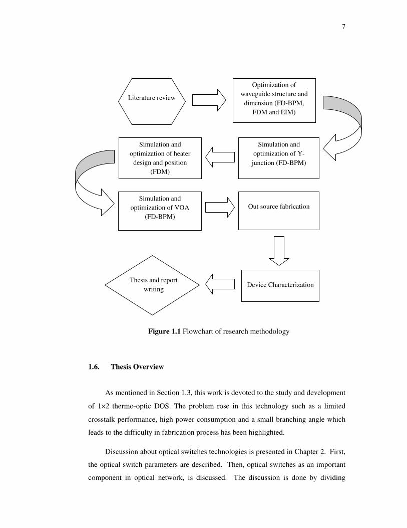
The research methodology was separated into eight main phases as shown in
Figure 1.1. The first phase is literature review to understand the problem, research
requirement, related current technology especially digital optical switch technology.
Through the literature review, the related theory and published works were
overviewed. The findings were used to define the objectives, scopes, and design
requirements for solving the problem of optical switch. The second phase is to select
the material and optimize the waveguide structure and dimension to be single mode
in the transmission window for today optical communication system. The modal
analysis was done using finite difference beam propagation methods (FD-BPM)
utilizes alternating direction implicit (ADI) method and finite difference method
(FDM) utilizes successive over relaxation (SOR) method. Semi-analytical method
was also done as comparison using effective index method (EIM). The third phase is
to simulate the structure of Y-junction using FD-BPM. The fourth phase is to
simulate and design the heater electrode to find the best position, dimension and
material to minimize the switching power using FDM which was accomplished by
MATLAB. The next phase is to design VOA in order to decrease the crosstalk. The
optimized design was then fabricated using coating, photolithography technique and
dry etching. Optical parameters which include crosstalk, insertion loss and
sensitivity to the input power of the fabricated devices were then measured to
investigate the device characteristics. The fabrications of the devices were done by
outsourcing.
7
1.6. Thesis Overview
As mentioned in Section 1.3, this work is devoted to the study and development
of 1×2 thermo-optic DOS. The problem rose in this technology such as a limited
crosstalk performance, high power consumption and a small branching angle which
leads to the difficulty in fabrication process has been highlighted.
Discussion about optical switches technologies is presented in Chapter 2. First,
the optical switch parameters are described. Then, optical switches as an important
component in optical network, is discussed. The discussion is done by dividing
Figure 1.1 Flowchart of research methodology
Optimization of
waveguide structure and
dimension (FD-BPM,
FDM and EIM)
Simulation and
optimization of Y-
junction (FD-BPM)
Simulation and
optimization of heater
design and position
(FDM)
Simulation and
optimization of VOA
(FD-BPM)
Literature review
Thesis and report
writing
Out source fabrication
Device Characterization

8
optical switches technologies into two major categories, namely interferometric
switches and non-interferometric switches. A review on published DOS is also
presented.
In order to gain sufficient information to define the design requirements for
solving the problem in DOS, fundamental theory of thermo-optic DOS is explained
in Chapter 3. The discussion starts from the optical waveguide technologies
available today and the light propagation in the waveguide. The modal analysis
methods such as EIM and FDM are briefly discussed. The behavior of light
propagation in Y-branch is discussed using coupled mode theory. An overview of
beam propagation method (BPM) is discussed briefly as the design and optimization
in this thesis is mainly accomplished by employing this method. At the end, thermal
analysis which is the fundamental in designing the optimum heater structure is
discussed.
Chapter 4 explains the simulation and optimization of the digital optical switch.
The optimization step starts from optimizing the waveguide structure. The
waveguide structure and dimension is optimized to be single mode in today optical
communication window (1.3 µm to 1.55 µm). The optimization of a Y-branch
constructed from the optimized waveguide was done by utilizing 3D BPM
simulations accomplished by BPM-CAD software from OptiWave. A new method
of heater design optimization was proposed. The optimization was then continued
to the optimization of VOA by employing BPM.
Based on the optimized design resulted in Chapter 4, the 1×2 Y-branch
waveguide and DOS without VOA was fabricated. The fabrication technique and
characterization of the fabricated devices are explained in chapter 5. The fabrication
technique includes coating, photolithography, dry etching and lift-off technique. The
measurement was done for crosstalk values, insertion loss and device sensitivity to
the input power.
Finally in Chapter 6, a concluding remarks and recommendations for future
prospects for this work are given.

REFERENCES
Abdalla, S., Ng, S., Barrios, P., Celo, D., Delâge, A., El-Mougy, S., Golub, I., He,
J.-J., Janz, S., McKinnon, R., Poole, P., Raymond, S., Smy, T. J., and Syrett,
B. (2004). Carrier Injection-Based Digital Optical Switch with
Reconfigurable Output Waveguide Arms. IEEE Photonics Technology
Letters. 16(4): 1038-1040.
Agrawal, G.E. (2002). Fiber-Optic Communication Systems. (3rd
ed.). New York:
John Wiley & sons, Inc.
Al-Azzawi, A. Fiber Optics: Principles and Practices. CRC Press Taylor &Francis
Group. 2007.
Augustsson, T. (2000). Proposal of a Bragg grating assisted MMIMI-coupler for
tunable add-drop multiplexing. IEEE Photonics Technology letters. 12(7):
918-920.
Bhatnagar, A., Suresh, Nair, K. R., Kumar, R., Chalapati, K. and Patro, Y.G.K.
(1994). Study of Cross Coupling in Transition Bends Using Cascade Coupler
Segment Method. IEEE Photonics Technology Letters. 6(8):1004-1007.
Bregni, S., Guerra, G., and Pattavina, A. (2001). State of the art of optical switching
technology for all-optical networks. Communications World. Rethymo,
Greece: WSES Press.
Burns, W.K. and Milton, A.F. (1975). Mode Conversion in Planar-Dielectric
Separating Waveguides. IEEE Journal of Quantum Electronics. QE-
11(1):32-39.
125
Burns, W.K. and Milton, A.F. (1977). Mode coupling in optical waveguide horns,
IEEE Journal of Quantum Electronics. QE-13:828-835.
Burns, W.K. and Milton, A.F. (1980). An Analytic Solution for Mode Coupling in
Optical Waveguide Branches. IEEE Journal of Quantum Electronics. QE-
16(4):446-454.
Chan, H. P., Chow, C. K., and Das, A. K. (2003). A Wide-Angle X-Junction
Polymeric Thermooptic Digital Switch with Low Crosstalk. IEEE Photonics
Technology Letters. 15(9):1210-1212.
Chaudri, C., Patil, D. S., and Gautam, D. K. (2001). A new Technique for reduction
of the power loss in the Y-branch optical power splitter. Optics
Communications. 193:121-125.
Chung, Y. and Dagli, N. (1990). An assessment of finite difference beam
propagation method. IEEE Journal of Quantum Electronics. 26:1335–1339.
Coldren, L.A. and Corzine, S.W. (1995). Diode Lasers and Photonic Integrated
Circuits. New York: John Wiley & Sons.
Diemeer, M.B.J. (1998). Polymeric thermo-optic space switches for optical
communications. Optical Materials. 9:192-200.
Dobbelaere, P. D., Falta, K., Fan, L., Gloeckner, S., and Patra, S. (2002). Digital
MEMS for optical switching. IEEE Communication Magazine. 40: 88–95.
Eldada, L. and Shacklette, L. W. (2000). Advances in Polymer Integrated Optics.
IEEE Journal of Selected Topics in quantum Electronics. 6(1):54-68.
Eldada, L., Blomquist, R., Maxfield, M., Pant, D., Boudouchian, G., Poga, C., and
Norwood, R.A. (1999). Thermooptic planar polymer Bragg Garting OADM’s
switch broad tuning range. IEEE Photonics Technology letters. 11(4): 448-
450.
126
Eldada, L., Fujita, J., Radojevic, A., Izuhara, T., Gerhardt R., Shi, J., Pant, D., Wang,
F., Malek, A. (2006). 40-Channel Ultra-Low-Power Compact PLC-Based
ROADM Subsystem. Optical Fiber Communication Conference, 2006 and
the 2006 National Fiber Optic Engineers Conference.
Garner, S.M. and Carraci, S. (2002). Variable Optical Attenuator for Large-Scale
Integration. IEEE Photonics Technology Letters. 14(11):1560-1562.
Grote, N., Venghaus, H. Fibre Optic Communication Devices. Springer. Berlin,
2001.
Hoekstra, H. J . W . M .. (2000). Optimisation of digital optical switches. Optical
and Quantum Electronics. 32: 843-854.
Hadley, G. R. (1992). Transparent boundary condition for the beam propagation
method. Optics Letters. 28:624.
Hadley, G. R. (1992). Wide-angle beam propagation using Pade approximant
operators. Optics Letter: 17.
Hadley, G.R. (1995). Full-Vector Waveguide Modeling Using an Iterative Finite-
Difference Method with Transparent Boundary Conditions. Journal of
Lightwave Technology. 13 (3):465-469.
Hattori, K., Fukui, M., Jinno, M., Oguma, M., and Oguchi, K. (1999). PLC-Based
Optical Add/Drop Switch with Automatic Level Control. Journal of
Lightwave Technology. 17(12): 2562-2571.
Hauffe, R. Integrated Optical Switching Matrices Constructed from Digital Optical
Switches Based on Polymeric Rib Waveguides. PhD Dissertation.
Technischen Universitat Berlin; 2002.
127
Hauffe, R., Siebel, U., Bruns, J., and Petermann, K. (2001). Digital Optical Switches
and Switching Matrices in Polymers. Int. J. Electron. Communication. 55(5):
305-312.
Heiblum, M., and Harris, J. H. (1975). Analysis of Curved Optical Waveguides by
Conformal Transformation. IEEE Journal of Quantum Electronics. QE-
11(2):75-83.
Hibino, Y., Kitagawa, T., Hill, K.O., Bilodeau, F., Malo, B., Albert, J., Johnson, D.C.
(1996). Wavelength division multiplexer with photoinduced Bragg gratings
fabricated in a planar-lightwave-circuit-type asymmetric Mach-Zehnder
interferometer on Si. IEEE Photonics Technology Letters. 8(1):84 – 86.
Hida, Y., Onose, H., Imamura, S. (1993). Polymer Waveguide Thermooptic Switch
with Low Electric Power Consumption at 1.3 µm. IEEE Photonics
Technology Letters. 5(7): 782-784.
Hiremath, K . R ., Hammeri, M ., Stoffer, R., Prkna, L. and , Tyoroky, J . C. (2005).
Analytic approach to dielectric optical bent slab waveguides. Optical and
Quantum Electronics. 37:37–61.
Hoffmann, M., Kopka, P., and Voges, E. (1998). Thermooptical Digital Switch
Arrays in Silica-on-Silicon with Defined Zero-Voltage State. Journal of
Lightwave Technology. 16(3):395-400.
Hoffmann, M., Kopka, P., Nusse, D., Voges E. (2003). Fibre-optical MEMS
switches based on bulk silicon micromachining. Microsystem Technologies.
9(5):299–303.
Huang, W. P. and Xu, C. L. (1993). Simulation of three-dimensional optical
waveguides by a full-vector beam propagation method. Journal of Quantum
Electronics. 29(10):2639 - 2649.
128
Hunsperger, R. G. (1984). Integrated optics: Theory and Technology. 2nd ed.
Berlin: Springer-Verlag.
Ibrahim, M.H. (2007). Polymer Based Multimode Interference Optical Devices. PhD
Thesis. Universiti Teknologi Malaysia, Skudai.
Ibrahim, M.H., Kassim, N. M., Mohammad, A.B., Gang, S.Y. (2004). Modelling of
Rib Waveguide Structure Using Effective Index Method. Elektrika. 6(1):43-
49.
Iodice, M., Mazzi, G., Sirletto, L. (2006). Thermo-optical static and dynamic
analysis of a digital optical switch based on amorphous silicon waveguide.
Optic Express. 4(12):5266-5278.
Ishida, O., Takahashi, H., and Inou Y. (1994). FDM-channel selection filter
employing an arrayed-waveguide grating multiplexer. Electronics
Letters.30(16): 1327-2328.
Jankowski, N.R., Bobcowski, C., Zipkin, D., Krchnavek, R.R., and Chamberlain,
R.D. (1999). MEMS-Based Optical Switch Design for Reconfigurable, Fault-
Tolerant Optical Backplanes. Proc. of the 6th Int'l Conf. on Parallel
Interconnects. 149-156.
Ji, C. –H., Yee, Y., Choi, J., Kim, S.-H., Bu, J.-U. (2004). Electromagnetic 2×2
MEMS optical switch. IEEE Journal of Selected Topics in Quantum
Electronics. 10(3): 545 – 550.
Jiang, X., Qi, Wei., Zhang, H., Tang, Y., Hao, Y., Yang, J., and Wang, M. (2006).
Low Crosstalk 1×2 Thermooptic Digital optical Switch with Integrated S-
Bend Attenuator. IEEE Photonics Technology Letters. 18(4): 610-612.
Jones, K.P., Chaudhry, M.S., Simeonidou, D., Taylor, N.H., and Morkel, P.R.
(1995). Optical wavelength add-drop multiplexer in installed submarine
WDM network. Electronics Letters. 31(24):2117-2118.

129
Jovanoski, Z., Towers, I.N., Ansari, N.A., Sammut, R.A. (2005). Approximate
analysis of circular bends in nonlinear planar waveguides. Optics
Communications. 244: 399–409.
Kashyap, R., Maxwell, G. D., and Ainslie, B. J. (1993). Laser-trimmed four port
bandpass filter fabricated in single-mode photosensitive Ge-doped planar
waveguide. IEEE Photonics Technology letters. 5(2): 191–194.
Keil, N., Yao, H.H. and Zawadzki, C. (1996). (2×2) Digital Optical Switch Realised
by Low Cost Polymer Waveguide Technology. Electronics Letters. 32(16):
1470-1471.
Keil, N., Yao, H. H., Zawadski, C. and Strebel, B. (1994). 4×4 polymer thermooptic
directional coupler switch at 1.55 µm. Electronics Letters. 30(8): 639-640.
Kim, K.-H., Kwon, M.-S., Shin, S.-Y., and Choi, D.-S. (2004). Vertical Digital
Thermooptic Switch in Polymer. IEEE Photonics Technology Letters.
16(3):783-785.
Kim, K.-H., Kwon, M.-S., Shin, S.-Y., and Choi, D.-S. 2004. Vertical Digital
Thermooptic Switch in Polymer. IEEE Photonics Technology Letters. 16(3):
783-785.
Kiniry, J. R. (1998). Wavelength Division Multiplexing: Ultra High Speed Fiber
Optics. IEEE Internet Computing.13-15.
Koai, K.T. and Liu, P.L. (1989). Modelling of Ti:LiNbO3 waveguide devices: Part
II-S-shaped channel waveguide bends. J. Lightwave Technology. LT-7: 1016-
1022.
Krahenbuhl, R., Howerton, M. M., Dubinger, J., and Greenblatt, A. S. (2002).
Performance and Modeling of Advanced Ti:LiNbO3 Doigital Optical Switch.
Journal of Ligthwave Technology. 20 (1). 92-98.

130
Krähenbühl, R., Howerton, M. M., Dubinger, J., and Greenblatt, A. S. 2002.
Performance and Modeling of Advanced Ti: LiNbO3 Digital Optical
Switches. IEEE Journal of Lightwave Technology. 20(1):92-99.
Kuo, I.-Y., Chang, C.-H., and Chen, Y.-K. (2001). In-Service OTDR Supervisory
DWDM System Directly Through Mach–Zehnder Fiber-Grating Optical
Add-Drop Multiplexers. IEEE Photonics Technology letters. 13(11): 1242-
1244.
Lauder, R.D.T., Badcock, J.M., Holloway, W.T., and Sampson, D.D. (1998). WDM
ring network employing a shared multiwavelength incoherent source. IEEE
Photonics Technology Letters.10(2): 294-296.
Lee, S.-S., Ahn, S.-W., Shin, S.-Y. (1997). Electro-optic polymer digital optical
switch with photobleached waveguides and a self-aligned electrode. Optics
Communications. 138:298-300.
Lee, S.-S., Bu, J.-U., Lee, S.-Y., Song, K.-C., Park, C. –G., and Kim, T.-S. (2000).
Low-Power Consumption Polymeric Attenuator Using a Micromachined
Membrane-Type Waveguide. IEEE Photonics Technology Letters. 12(4):
407-409.
Leisching, P., Bock, H., Richter, A., Glingener, C., Pace, P., Keyworth, B.,
Philipson, J., Farries, M., Stoll, D., and Fischer, G. (2000). All-optical-
betworking at 0.8 Tb/s using reconfigurable optical add/drop multiplexer.
IEEE Photonics Technology letters. 12(7): 918-920.
Liaw, S.-H., Ho, K. –P., Chen, Y.-K., Lee, C.-C. (1999). Reconfigurable WDM
add/drop multiplexer based on optical switches and fibre Bragg gratings.
Optical and Quantum Electronics. 31: 77-83.
131
Liu, P.L., Li, B.J., Cressman, P. J., Debesis, J. R. and Stoller, S. (1991). Comparison
of measured Losses of Ti:LiNbO3 Channel Waveguide Bends. IEEE Photonic
Technology Letters. 3(8):755-756.
Liu, Q.Z, Jiang, X.S., Yu, L.S., Guan, Z.F., Yu, P.K.L., and Lau, S.S. (1995). A
novel processing technique to fabricate planar InGaAsP/InP electroabsorption
waveguide modulators. J. Electron. Mater. 24:991–997.
Lo, Y.-L., Chow, H.-C., and Chiang, C.-Y. (2004). Reconfigurable OADM and OXC
designed by a new optical switch. Optical Fiber Technology.10:187–200.
Low, Y. L., Scotti, R. E., Ramsey, D. A., Bolle, C. A., O'Neill, S. P. and Nguyen, K.
C. (2003). Packaging of Optical MEMS Devices. J. Electron.
Packag. 125(3):325-328.
Lu, Y.Y., and Ho, P.L. (2002). Beam Propagation Modeling of Arbitrarily Bent
Waveguides. IEEE Photonics Technology Letters. 14(12):1698-1700.
Ma, X., and Kuo, G. -S. (2003). Optical Switching Technology Comparison: Optical
MEMS Vs. Other Technologies. IEEE Optical Communications. S16-S23.
Ma, X., Kuo, G.-S., (2004). A novel integrated multistage optical MEMS-mirror
switch architecture design with shuffle Benes inter-stage connecting
principle. Optics Communications. 242:179–189.
Majumdar, P. (2005). Computational Methods for Heat Transfer. New York: Taylor
& Francis.
Mechin, D., Grosso, P., and Bosc, D. (2001). Add-drop multiplexer with UV-written
Bragg gratings and directional coupler in SiO2-Si integrated waveguides,
Journal of Lightwave Technology. 19(9): 1282-1286.
132
Minford, W.J., Korotky, S.K., and Alferness, R.C. (1982). Low-loss Ti:LiNbO3
waveguide bends at 1.3 µm. IEEE J.Quantum Electron. QE-18 (10):1802-
1806.
Mitomi, O., Kasaya, K. (1997). Wide-angle finite-element beam propagation
method using Pade approximation. Electronics Letters. 33(17):1461 – 1462.
Moosburger, R. and Petermann, K. (1998). 4 ×4 Digital Optical Matrix Switch Using
Polymeric Oversized Rib Waveguide. IEEE Photonics Technology Letters.
10(5):684-686.
Moosburger, R., Kostrzewa, C., Fischbeck, G., and Petermann, K. (1997). Shaping
the Digital Optical Switch Using Evolution Strategies and BPM. IEEE
Photonics Technology Letters. 9(11):1484-1486.
Morris, A. S. III. (2001). In Search of Transparent Networks. IEEE Spectrum.
38(10): 47-51.
Mustieles, F.J., Ballesteros, E., and Baquero, P. (1993). Theoritical S-Bend Profile
for Optimization of Optical Waveguide Radiation Losses. IEEE Photonics
Technology Letters. 5 (5): 551-553.
Nelson, W. H., Choudhury, A. N. M. M., Abdalla, M., Bryant, R., Meland, E., and
Niland, W. (1994). Wavelength-and polarization-independent large angle
InP/InGaAsP digital optical switches with extinction ratios exceeding 20 dB.
IEEE Photonics Technology Letters. 6:1332–1334.
Ng, S., Abdalla, S., Barrios, P., Delage, A., Janz, S., McKinnon, R. and Syrett, B.
(2005). Bend loss attenuator by carrier injection in InGaAs/InP. Electronics
letters. 41(24).
Nishihara, H., Haruna, M., Suhara, T. Optical Integrated Circuits. Mc Graw-Hill.
USA, 1985.

133
Noh, Y.-O., Lee, C.-H., Kim, J.-M., Hwang, W.-Y., Won, Y.-H., Lee, H.-J., Han, S.-
G., and Oh, M.-C. (2004a). Polymer waveguide variable optical attenuator
and its reliability. Optics Communications. 242: 533–540.
Noh, Y.-O, Kim, J.-M., Yang, M.-S , Choi, H.-J., Lee, H.-J., Won, Y. -H, and Han,
S.-G. (2004b). Thermooptic 2 ×2 Asymmetric Digital Optical Switches with
Zero-Voltage Operation State. IEEE Photonics Technology Letters. 16(2):
446-448.
Noh, Y.O., Lee, H.-J., Won, Y. -H., and Oh, M.-C. (2006). Polymer Waveguide
Thermo-optic Switches with -70 dB Optical Crosstalk. Optics
Communications. 258:18-22.
Okayama, H., Kawahara, M. (1993). Reduction of Voltage-Length Product for Y-
Branch Digital Optical Switch. Journal of Lightwave Technology. 11(2):379-
387.
Okuno, M., Goh., T., Sohma, S., and Shibata, T. (2003). Recent Advances in
Optical Switches Using Silica-based PLC Technology. NTT Technical
review. 1(7): 20-30.
Ollier, E. (2002). Optical MEMS Devices Based on Moving Waveguides. IEEE J.
Sel. Topics Quantum Elect. 8(1):155–62.
Papdimitriou, G. I., Papazoglou, C., and Pomportsis, A. S. (2003). Optical
Switching: Switch Fabrics, Techniques, and Architectures. Journal of
Ligthwave Technology. 21(2): 384-405.
Park, H.S., Yun, S.H., Hwang, I.K., Lee, S.B., and Kim, B.Y. (2001). All-fiber add-
drop wavelength-division multiplexer based on intermodal coupling. IEEE
Photonics Technology letters. 13(5): 460-462.
134
Rivera, M. (1995). A Finite Difference BPM Analysis of Bent Dielectric
Waveguides. Journal of Lightwave Technology. 13 (2): 233-238.
Riziotis, C. and Zervas, M.N. (2001). Design consideration in optical add/drop
multiplexers based on grating-assisted null couplers. Journal of Lightwave
Technology. 19(1): 92-104.
Saida, T., Kaneko, A., Goh, T., Okuno, M., Himeno, A., Takiguchi, K., and
Okamoto, K. (2000). A thermal silica-based optical add/drop multiplexer
consisting of arrayed waveguide gratings and double gate thermooptic
switches. Electronics Letters. 36(6): 528-529.
Scarmozzino, R., Gopinath, A., Pregla, R., and Helfert, S. (2000). Numerical
Techniques for Modeling Guided-WavePhotonic Devices. IEEE Journal of
Selected Topics in Quantum Electronics. 6(1):150-162.
Senior, J. M. (1992). Optical fiber communications : principles and practice. (2nd
ed.). New York: Prentice-Hall.
Shankar, R. , Florjanczyk, M., Hall, T. J., Vukovic, A., and Hua, H. (2007). Multi-
degree ROADM based on wavelength selective switches: Architectures and
scalability. Optics Communications. 279: 94–100.
Siebel, U., Hauffe, R., and Petermann, K. (2000). Crosstalk-enhanced Polymer
Digital Optical Switch based on W-shape. IEEE Photonics Technology
Letters. 12(1): 40-42.
Siebel, U., Hauffe, R., Burns, J., and Petermann, K. (2001). Polymer Digital Optical
Switch with an Integrated Attenuator. IEEE Photonics Technology Letters.
13(9): 957-959.
Silberberg, Y., Perimutter, P., and Baran, J. E. (1987). Digital Optical Switch. App.
Phys. Letter. 51(16):1230-1232.

135
Sirleto, L., Iodice, M., Della Corte, F.G., and Rendin, I. (2007). Digital optical
switch based on amorphous silicon waveguide. Optical Laser Engineering.
45: 458-462.
Sneh, A., Zucker, J. E., Miller, B. I., and Stulz, L. W. (1997). Polarization-
Insensitive InP-Based MQW Digital Optical Switch. IEEE Photonics
Technology Letters. 9(12):1589-1591.
Song, Y.W., Pan, Z., Starodubov, D., Grubsky, V., Salik, E., , Havstad, S.A, Xie, Y.,
Willner, A.E. and Feinberg, J. (2001). All-fiber WDM optical cross connect
using ultrasong widely tunable FBGs. IEEE Photonics Technology letters.
13(10):1103-1105.
Supa’at, A. S. M. (2004). Design and Fabrication of a Polymer Based Directional
Coupler Thermooptic Switch. PhD Thesis. Universiti Teknologi Malaysia,
Skudai.
Supa’at, A.S.M., Ibrahim, M.H., Mohammad, A.B., Kassim, N. M. and Ghazali, N.
E. (2008). A Novel Thermooptic Polymer Switch Based on Directional
Coupler Structure. American Journal of Applied Sciences. 5(11):1552-1557.
Supa’at, A.S.M., Mohammad, A.B., Kassim, N.M. (2004). Polymer Based
Directional Coupler Thermooptic Optical Switch. Jurnal Teknologi Universiti
Teknologi Malaysia. 40(D):1–8.
Suzuki, H., Fujiwara, M., and Iwatsuki, K. (2006). Application of Super-DWDM
Technologies to Terrestrial Terabit Transmission Systems. Journal of
Lightwave Technology. 24(5): 92-104.
Toyoda, S., Ooba, N., Katoh, Y., Kurihara, T. and Maruno, T. (2000). Low crosstalk
and low loss 2×2 thermo-optic digital optical switch using silicone resin
waveguides. Electronics Letters. 36(21):1803-1804.
136
Veneman, J. Design and Characterization of a Thermo-optic 2×2 Switch. Msc.
Thesis. University of Twente; 2002.
Vinchant, J. F., Renaud, M., Goutelle, A., Erman, M., Svensson, P., and Thylen, L.
(1992). Low driving voltage or current digital optical switch on InP for
multiwavelength system applications. Electronics Letters. 28:1135–1137.
Wang, W.-K., Lee, H. J. and Anthony, P. J. (1996). Planar Silica-Glass Optical
Waveguides with Thermally Induced Lateral Mode Confinement. IEEE
Journal of Lightwave Technology. 14(3): 429-436.
Wang, Z.F., Cao, W., Shan, X.C., Xu, J.F., Lim, S.P., Noell, W., and de Rooij, N.F.
(2004). Development of 1 × 4 MEMS-based optical switch. Sensors and
Actuators A. 114: 80–87.
Yamamoto, T., Yamaguchi, J., Takeuchi, N., Shimizu, A., Sawada, R., Higurashi, E.
and Uenishi, Y. (2004). A Three-Dimensional Micro-Electro-Mechanical
System (MEMS) Optical Switch Module Using Low-Cost Highly Accurate
Polymer Components. J. Appl. Phys. 43:5824-5827.
Yang, M.-S., Noh, Y.O., Won, Y.H. and Hwang, W.-Y. (2001). Very low crosstalk
1×2 digital optical switch integrated with variable optical attenuators.
Electronics Letters. 37(9):587-588.
Yang, Y.-J., Liao, B.-T., and Kuo, W. –C. (2007). A novel 2 × 2 MEMS optical
switch using the split cross-bar design. J. Micromech. Microeng. 17: 875-
882.
Yeo, D.-M., and Shin, S.-Y. (2006). Polymer-silica hybrid 1 × 2 thermooptic
switch with low crosstalk. Optics Communications. 267: 388–393.
Yuan, W., Kim, S., Sadowy, G., Zhang, C., Wang, C., Steier, W.H. and Fetterman,
H.R. (2004). Polymeric electro-optic digital optical switches with low
switching voltage. Electronics Letters. 40(3):195-197.

137
Yuan, W., Kim, S., Steier, W. H., and Fetterman, H. R. (2005). Electrooptic
Polymeric Digital Optical Switches (DOSs) With Adiabatic Couplers. IEEE
Photonics Technology Letters. 17(12):2568-2570.
Yuan, W., Kim, S., Fetterman, H. R., Steier, W. H., Jin, D., and Dinu, R. (2007).
Hybrid Integrated Cascaded 2-bit Electrooptic Digital Optical Switches
(DOSs). IEEE Photonics Technology Letters. 19 (7): 519-521.