icme 2004© 2004 marilyn wolf architectures for multimedia computing 3: dsps and systems-on- chips...
TRANSCRIPT

ICME 2004 © 2004 Marilyn Wolf
Architectures for Multimedia Computing3: DSPs and Systems-on-Chips
Marilyn Wolf
Dept. of Electrical Engineering
Princeton University

What is a DSP?
Traditional definition: Harvard architecture. Multiplier-accumulator.
Today: Marketing term (every CPU is a DSP).
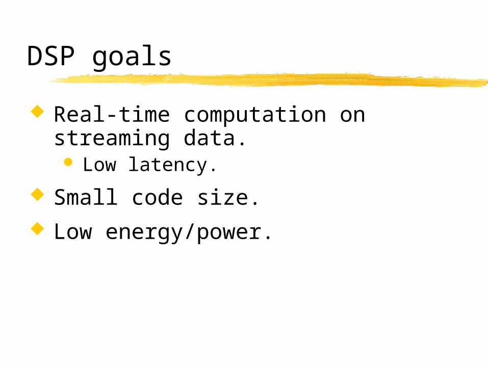
DSP goals
Real-time computation on streaming data. Low latency.
Small code size. Low energy/power.

TI C54x architectural features
40-bit ALU + barrel shifter. Multiple internal busses: 1
instruction, 3 data, 4 address. 17 x 17 multiplier. Single-cycle exponent encoder. Two address generators with
dedicated registers.

TI C54x instruction set features
Specialized instructions for Viterbi. Repeat and block repeat
instructions. Instructions that read 2, 3 operands
simultaneously. Conditional store. Fast return from interrupt.
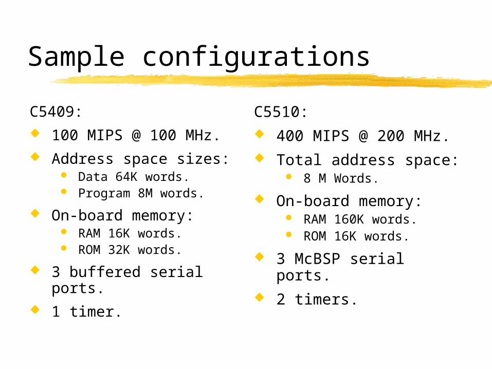
Sample configurations
C5409: 100 MIPS @ 100 MHz. Address space sizes:
Data 64K words. Program 8M words.
On-board memory: RAM 16K words. ROM 32K words.
3 buffered serial ports. 1 timer.
C5510: 400 MIPS @ 200 MHz. Total address space:
8 M Words.
On-board memory: RAM 160K words. ROM 16K words.
3 McBSP serial ports. 2 timers.

Single-instruction repeat loop example
STM #4000h,AR2
; load pointer to source
STM #100h,AR3
; load pointer to destination
RPT #(1024-1)
MVDD *AR2+,*AR3+
; move
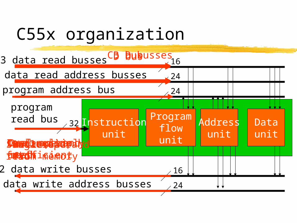
C55x organization
Instructionunit
Programflowunit
Addressunit
Dataunit
3 data read busses
3 data read address busses
program address bus
programread bus
2 data write busses
2 data write address busses
16
24
24
16
24
32
InstructionfetchData readfrom memory
D bus
Single operandread
C, D busses
Dual operandread
B bus
Dual-multiplycoefficientWrites

C55x low power features
Parallel execution units---longer idle shutdown times.
Multiple data widths: 16-bit ALU vs. 40-bit ALU.
Instruction caches minimizes main memory accesses.
Power management: Function unit idle detection. Memory idle detection. User-configurable IDLE domains allow
programmer control of what hardware is shut down.

C5x McBSP serial ports
Designed to interface to devices. Full, duplex; double-buffered transmission;
triple-buffered reception. Works with interrupts or DMA. Separate xmit, rcv clock, highly
programmable. -law, A-law companding. Direct interface to codecs, T1/E1 framers,
MVIP framers, etc.

McBSP block diagram16-bit peripheral bus
Registersfor sync
control andmonitoring
Registers formultichannelcontrol andmonitoringco
mpa
nd
Data rcv, xmit clock
interrupt DMA
Clock/frame sync

Image/video hardware extensions
Available in 5509 and 5510. Equivalent C-callable functions for
other devices.
Available extensions: DCT/IDCT. Pixel interpolation Motion estimation.

DCT/IDCT
2-D DCT/IDCT is computed from two 1-D DCT/IDCT. Put data in
different banks to maximize throughput.
block
Column DCT
interim DCTRowDCT

C55 DCT/IDCT coprocessor extensions
Load, compute, transfer to accumulators: ACy=copr(k8,ACx,Xmem,Ymem)
Compute, transfer, mem write: ACy=copr(k8,ACx,ACy), Lmem=ACz
Special: ACy=copr(k8,ACx,ACy)

Software pipelined load/compute/store for DCT
Iteration i-1
Dual_load
8compute
4Long_store
4 empty
3Dual_load
empty
Iteration i
Dual_load
8compute
4Long_store
4 empty
3Dual_load
empty
Iteration i+1
Dual_load
8compute
4Long_store
4 empty
3Dual_load
empty
op_i(0), load_i+1(0,1)op_i(1), store_i-1(0,1)op_i(2), store_i-1(2,3)op_i(2), store_i-1(4,5)op_i(2), store_i-1(6,7)op_i(2), load_i+1(2,3)…

C55 motion estimation
Search strategy: Full vs. non-full.
Accuracy: Full-pixel vs. half-pixel.
Number of returned motion vectors: 1 (one 16x16) vs. 4 (four 8x8).
Algorithms: 3-step algorithm (distance 4,2,1). 4-step algorithm (distance 8,4,2,1). 4-step with half-pixel refinement.

Four-step motion estimation breakdown
d = {8,4,2,1};
for (i=0; i<4; i++) {
compute 3 upper differences for d[i];
compute 3 middle differences for d[i];
compute 3 lower differences for d[i];
compute minimum value;
move to next d;
}
X

C55 motion estimation accelerator
Includes 3 16-bit pixel data paths, 3 16-bit absolute differences (ADs).
Basic operation: [ACx,ACy] =
copr(k8,ACx,ACy,Xmem,Ymem,Coeff) K8 = control bits (enable AD units, etc.) ACx, ACy = accumulated absolute differences Xmem, Ymem = pointers to odd, even lines of
the search window Pointer to two adjacent pixels from reference
window

C55 pixel interpolation
Given four pixels A, B, C, D, interpolate three half-pixels:
A B
C D
U
M R

Pixel interpolation coprocessor operations
Load pixels and compute: ACy=copr(k8,AC,Lmem)
Load pixels, compute, and store: ACy=copr(k8,AACx,Lmem) ||
Lmem=ACz

Motorola 56301
24-bit word. 80 MIPS @ 80 MHz, 100 MIPS @ 100 MHz. 24x24 multiplier, 56-bit barrel shifter. On-chip instruction cache controller. Nested hardware DO loops. On-chip memory:
RAM 1024 -> 4096 words. X data RAM 2048 -> 3072 words. Y data RAM 2048 -> 3072 words.

TI C62/C67
Up to 8 instructions/cycle.32 32-bit registers.Function units:
Two multipliers.Six ALUs.
All instructions execute conditionally.

TI C6x data operations
8/16/32-bit arithmetic.40-bit operations.Bit manipulation operations.

C6x system
On-chip RAM.32-bit external memory: SDRAM,
SRAM, etc.Host port.Multiple serial ports.Multichannel DMA.32-bit timer.

C6x block diagram
Data path 1/Reg file 1
Data path 2/Reg file 2
Execute DMA
timers
Serial
Program RAM/cache512K bits
Data RAM512K bits
JTAG
PLL
bus

C6x data paths
General-purpose register files (A and B, 16 words each).
Eight function units:.L1, .L2, .S1, .S2, .M1, .M2, .D1, .D2
Two load units (LD1, LD2).Two store units (ST1, ST2).Two register file cross paths (1X and 2X).Two data address paths (DA1 and DA2).
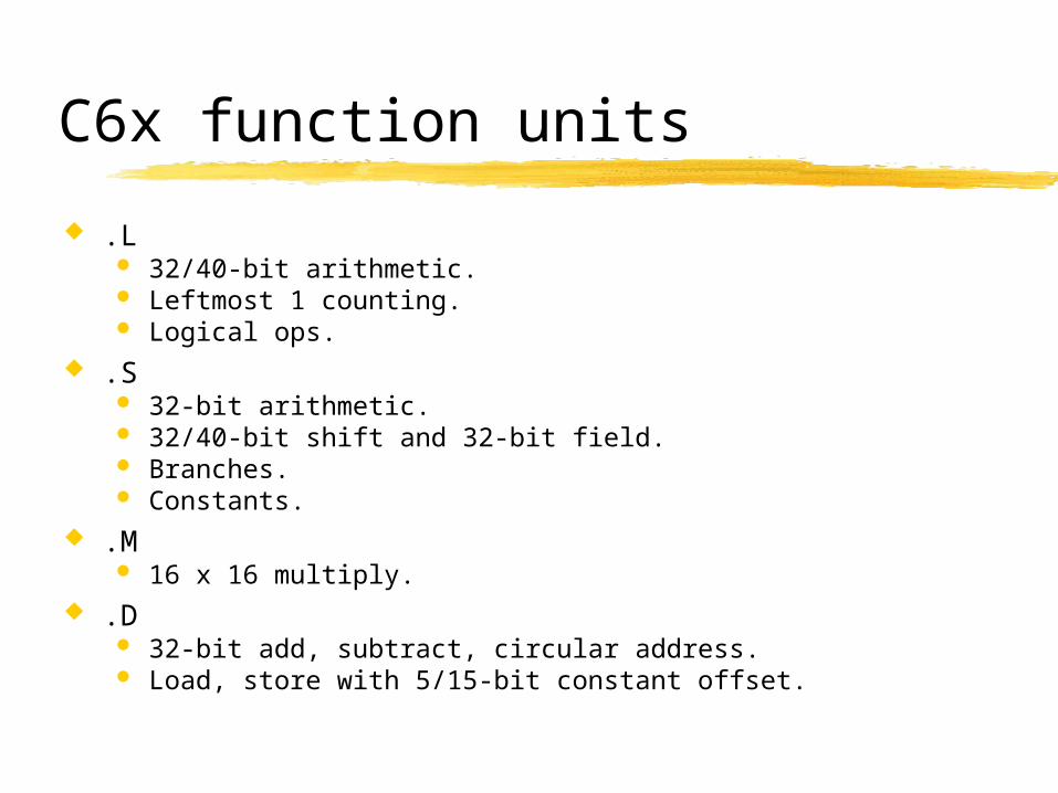
C6x function units
.L 32/40-bit arithmetic. Leftmost 1 counting. Logical ops.
.S 32-bit arithmetic. 32/40-bit shift and 32-bit field. Branches. Constants.
.M 16 x 16 multiply.
.D 32-bit add, subtract, circular address. Load, store with 5/15-bit constant offset.

Motorola Starcore SC140
DALU includes 4 ALUs, 1 register file. AGU includes 2 address arithmetic
units (AAU), 1 address register file. Program sequencer and control unit
(PSEQ). Performance:
4 million MACs per second per MHz clock. 10 RISC MIPS per MHz clock.

Typical SC140 configuration
Level 1 memory expansionRAM, ROM
peripherals
DMA,Cache,
Interrupts,Level 2 mem,
Etc.
Program sequencer
ALUALUALUALU
AAUAAU
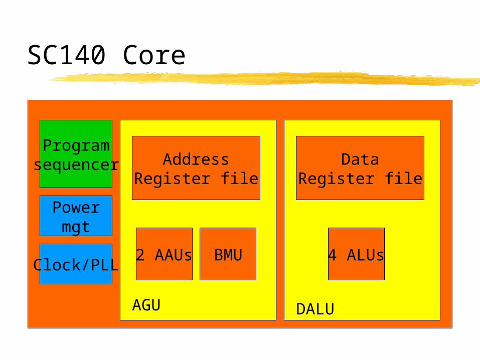
SC140 Core
Programsequencer
Powermgt
Clock/PLL
AGU DALU
AddressRegister file
2 AAUs BMU
DataRegister file
4 ALUs

Instruction format
16-bit instructions. Up to 6 instructions per cycle. Instructions are grouped to define
allowable simultaneous operations.
MACR –D0,D1,D7 AND D4,D5 MOVE.L (R0),+N0,R6 ADDA R2,R3
DALU AGU

AGU addressing
Allowable addressing modes: Linear. Modulo. Reverse-carry. Automatic updating during register
indirect. Stack.
Array addressing: base, offsett, modifier registers.
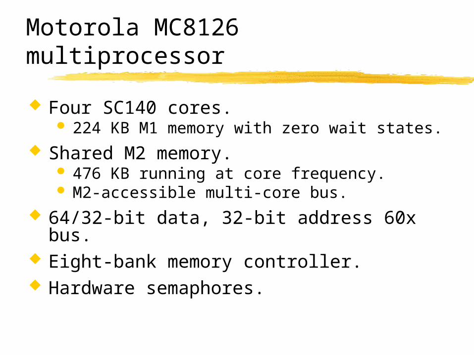
Motorola MC8126 multiprocessor
Four SC140 cores. 224 KB M1 memory with zero wait states.
Shared M2 memory. 476 KB running at core frequency. M2-accessible multi-core bus.
64/32-bit data, 32-bit address 60x bus. Eight-bank memory controller. Hardware semaphores.

TM-1 characteristics
Characteristics Floating point
support Sub-word
parallelism support If Conversion Additional custom
operations

Trimedia TM-1
memory interface
video in
audio in
I2C
timers
image co-p
PCI
video out
audio out
serial
VLD co-p
VLIW CPU

TM-1 VLIW CPU
register file
read/write crossbar
FU1 FU27
slot 1 slot 2 slot 3 slot 4 slot 5
...

Embedded vs. scientific applications
Embedded applications provide task-level parallelism.
Embedded applications run many different types of algorithms at once.

Scientific numerical calculation
Partition a large calculation across multiple processors:
CPU CPU CPU…

Task level parallelism
Map tasks on to multiprocessor:
PE 1 PE 2 PE 3+
application architecture
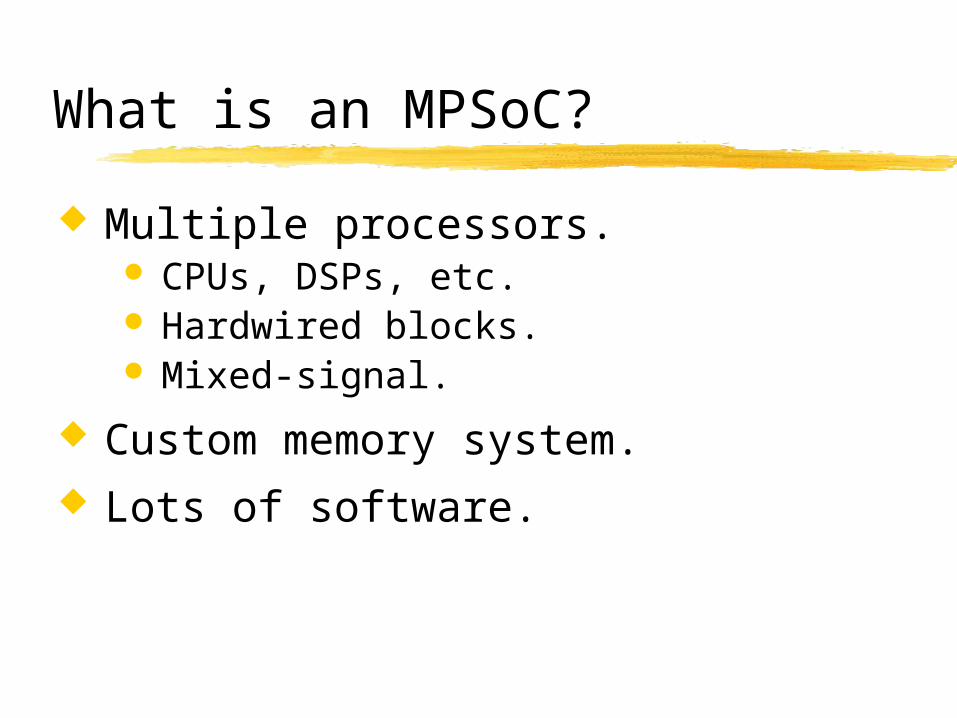
What is an MPSoC?
Multiple processors. CPUs, DSPs, etc. Hardwired blocks. Mixed-signal.
Custom memory system. Lots of software.

MPSoC applications
Sophisticated markets: High volume. Demanding performance, power
requirements. Strict price restrictions.
Often standards-driven. Multimedia is an ideal application.

Why multiple platforms?
People still care about cost.People care about power
consumption.Sufficiently general solutions don’t fit
on one chip.
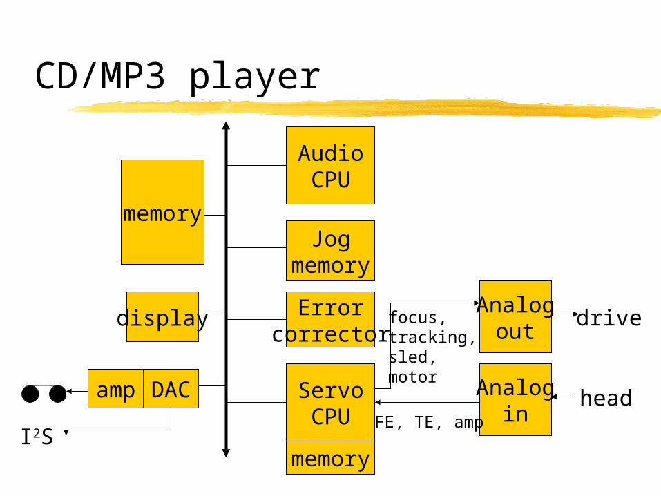
CD/MP3 player
AudioCPU
amp
Jogmemory
Errorcorrector
ServoCPU
Analogin
Analogout
FE, TE, amp
focus,tracking,sled,motor
head
drive
memory
memory
display
DAC
I2S
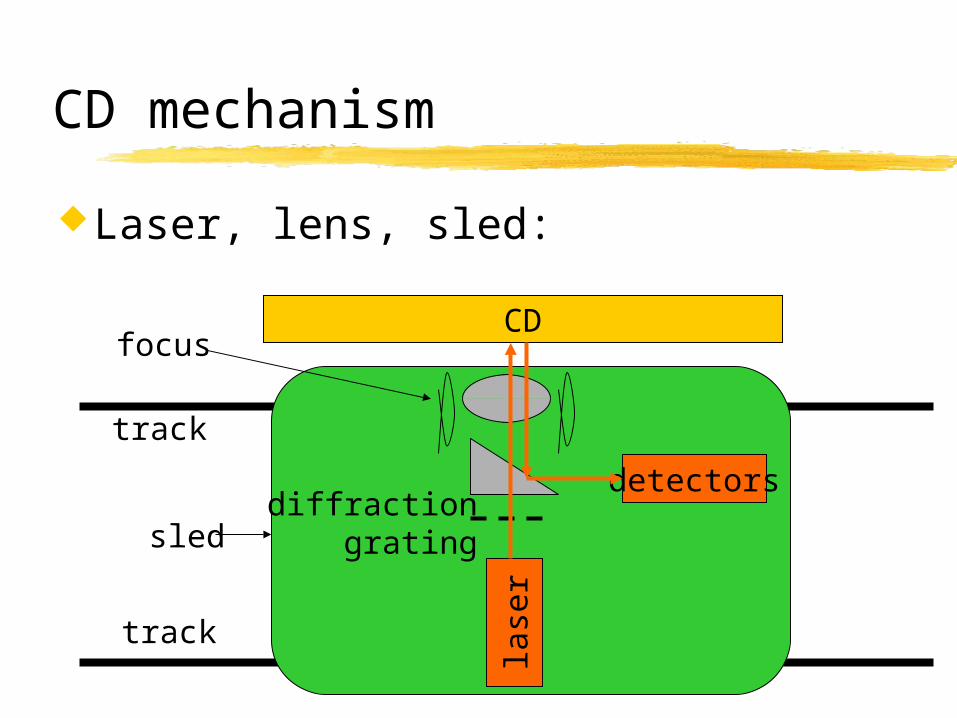
CD mechanism
Laser, lens, sled:
lase
r
CD
detectorsdiffraction
gratingsled
track
track
focus

Servo control
Four main signals:focus (laser) @ 245 kHz;tracking (laser) @ 245 kHz;sled (motor): @ 800 Hz;Disc motor.
Optical pickup

Control and error correction
Skips caused by physical disturbance. Wait for disturbance to subside. Retry.
Read errors caused by disc/servo problems. Detect error. Choose location for retry. Retry. Fail and interpolate.

DVD player
Yasuda, et al (Matsushita): two-chip solution for DVD back-end.Video MPEG 2 at Main Level (MP2@ML).Audio AC-3.External 16 Mb SDRAM.

DVD back-end
MPEG2stream
demux
AC-3Audio decoder
MPEG2Video decoder
Subpicturedecoder
Colorencoder
+
SDRAM

Video decoder
Hostinterface
RISCcontroller
Micro-program
Streamparser
Macroblockpipeline
VideoOutput
core
PLL SDRAM interface
system
audio

Macroblock pipeline
Allowed processing time:[30 rows*45 macroblocks/row]/29.97 Hz
=24.71 s.
Three stages in pipeline:Variable-length decode.Inverse quantize/inverse DCT, motion
compenstation.Reconstruction combines IQ/IDCT + MC.

Viper set-top box SoC
MIPS Trimedia
Off-chip SDRAM
MC bridge TC bridge
Bus ctrlBus ctrl
Clocks,DMA,Reset,debug
I2C, Smcard
PCI
USB, 1394
MMIbus
MBS
2D AICP
MPEG
SPDIF
GPIO
C bridge

Bus requirements
Separate cache and register-access traffic.
Separate register-access traffic of the two CPUs.
Each CPU has a high-performance, low-latency path to memory.
Each CPU has low-latency access to its peripherals.

Bus structure
MMI bus goes to bulk memory. Point-to-point design. 64-bit, 143 MHz. Round-robin arbitration. Controller separates on-chip accesses.
PI bus for peripherals. Tri-state design. Compatible with existing IP for peripherals. Fast-PI for high-speed MIPS peripherals. MIPS-PI for generic MIPS peripherals. T-PI for Trimedia peripherals.

TI OMAP
Targets communications, multimedia.
Multiprocessor with DSP, RISC.
C55x DSP
OMAP 5910:
ARM9
MMU
Memory ctrl
MPUinterface
SystemDMA
control
bridge
I/O

ST Nomadik
Targets mobile multimedia.
A multiprocessor-of-multiprocessors.
ARM9
Mem
ory
syst
em
I/O
bri
dges
Audioaccelerator
Videoaccelerator
heterogeneousmultiprocessors

ST MMDSP+
Embedded processor core used in multiple chips: Runs at 175 MHz. 1 cycle per instruction. 2-level instruction cache. 16/24-bit fixed point. 32-bit floating point. C programmed Fully synthesizable.

Nomadik video accelerator
MMDSP+data
RAMinstrRAM
Xbus
Interruptcontroller
Picturepost
processing
Videocodec
Pictureinput
processing
Localdatabus
MasterAHBDMA

Nomadik audio processor
SlaveAHB
Timers, GPIO, etc.
MMDSP+Y RAMX RAMInstrcache
ARMDMA
DMA1 DMA2
MasterAHB
X Bus
Y Bus
Nomadik support
Supports OMAPI standard. Standard includes mid-level driver
APIs.
Nomadik defines: Base operating system. Base drivers. Multimedia accelerators and their
drivers.

FPGAs
Can be used to provide hardware acceleration. First-generation Replay.
Platform FPGAs provide CPU, FPGA fabric.
FPGA trade-offs: Low design cost. Higher incremental cost in large volumes. Higher power consumption than custom.

Xilinx Virtex II Pro
Up to 4 PowerPC 405s per chip:
5 stage pipe, static branch prediction, etc.
Separate instruction, data caches.
MMU. Timers.
PowerPC
FPGA fabric