id 112c:mcu architecture evolution now better than … · id 112c:mcu architecture evolution –...
TRANSCRIPT

Renesas Electronics America Inc.
© 2010 Renesas Electronics America Inc. All rights reserved.
ID 112C: MCU Architecture Evolution – Now Better than Ever – So who’s the Best?
Mark Rootz
Sr. Marketing Manager
12 October 2010
Version: 1.2

2 © 2010 Renesas Electronics America Inc. All rights reserved.
Mark Rootz
Renesas Sr. Marketing Manager, 32-bit MCUs
Definition and Promotion of 32-bit MCUs, N. America
BSEE and MSEE from University of Missouri – Rolla
Seven years at STMicroelectronics
Marketing Manager, STR9 32-bit ARM9 MCU line (France)
Product Marketing Manager, uPSD 8-bit 8051 MCU (San Jose CA)
Product definition, technical marketing, business mgt, infrastructure
Three years at Waferscale Inc
Applications Manager, uPSD MCUs
Tools, software, training, documentation, solutions, silicon validation
Three years at Hypertech Inc
Project Manager and engineering
Automotive powertrain controller software and hardware
Twelve years at McDonnell Aircraft (now Boeing)
Project Manager and engineering
F15/F18 fighter avionics systems engineering (weapons, radar, navigation)
Real-time simulation/test environment for complete avionics suite
Embedded MCUs, MPUs, PLDs software and hardware design

3 © 2010 Renesas Electronics America Inc. All rights reserved.
Renesas Technology and Solution Portfolio
Microcontrollers
& Microprocessors #1 Market share
worldwide *
Analog and
Power Devices #1 Market share
in low-voltage
MOSFET**
Solutions
for
Innovation ASIC, ASSP
& Memory Advanced and
proven technologies
* MCU: 31% revenue
basis from Gartner
"Semiconductor
Applications Worldwide
Annual Market Share:
Database" 25
March 2010
** Power MOSFET: 17.1%
on unit basis from
Marketing Eye 2009
(17.1% on unit basis).

4 © 2010 Renesas Electronics America Inc. All rights reserved.
4
Renesas Technology and Solution Portfolio
Microcontrollers
& Microprocessors #1 Market share
worldwide *
Analog and
Power Devices #1 Market share
in low-voltage
MOSFET**
ASIC, ASSP
& Memory Advanced and
proven technologies
* MCU: 31% revenue
basis from Gartner
"Semiconductor
Applications Worldwide
Annual Market Share:
Database" 25
March 2010
** Power MOSFET: 17.1%
on unit basis from
Marketing Eye 2009
(17.1% on unit basis).
Solutions
for
Innovation
5 © 2010 Renesas Electronics America Inc. All rights reserved.
5
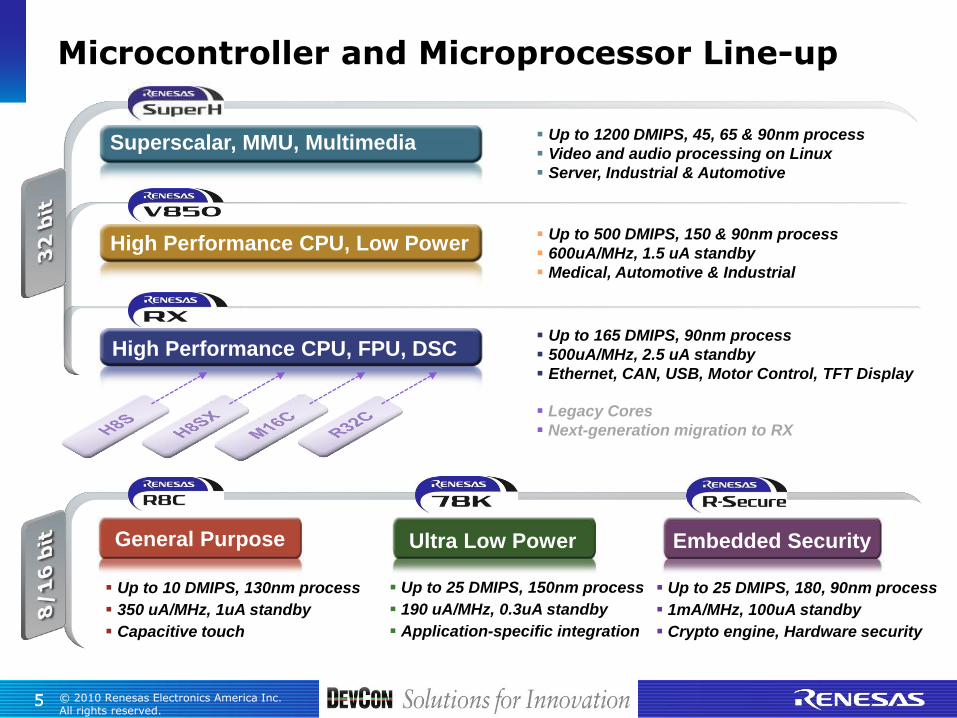
Microcontroller and Microprocessor Line-up
Superscalar, MMU, Multimedia Up to 1200 DMIPS, 45, 65 & 90nm process
Video and audio processing on Linux
Server, Industrial & Automotive
Up to 500 DMIPS, 150 & 90nm process
600uA/MHz, 1.5 uA standby
Medical, Automotive & Industrial
Legacy Cores
Next-generation migration to RX
High Performance CPU, FPU, DSC
Embedded Security
Up to 10 DMIPS, 130nm process
350 uA/MHz, 1uA standby
Capacitive touch
Up to 25 DMIPS, 150nm process
190 uA/MHz, 0.3uA standby
Application-specific integration
Up to 25 DMIPS, 180, 90nm process
1mA/MHz, 100uA standby
Crypto engine, Hardware security
Up to 165 DMIPS, 90nm process
500uA/MHz, 2.5 uA standby
Ethernet, CAN, USB, Motor Control, TFT Display
High Performance CPU, Low Power
Ultra Low Power General Purpose

7 © 2010 Renesas Electronics America Inc. All rights reserved.
7
RX: Performance without Sacrafice
High Performance CPU, FPU, DSC
High Performance CPU, Low Power
Superscalar, MMU, Multimedia Up to 1200 DMIPS, 45, 65 & 90nm process
Video and audio processing on Linux
Server, Industrial & Automotive
Up to 500 DMIPS, 150 & 90nm process
600uA/MHz, 1.5 uA standby
Medical, Automotive & Industrial
High Performance CPU, Low Power
Legacy Cores
Next-generation migration to RX
Up to 165 DMIPS, 90nm process
500uA/MHz, 2.5 uA standby
Ethernet, CAN, USB, Motor Control, TFT Display
Key Attributes

8 © 2010 Renesas Electronics America Inc. All rights reserved.
There are many 32-bit MCU/DSP Architectures
covering varied capabilities
RX Innovation – Single Chip Enablement
PIC32
CortexM3/M4 Coldfire
Kinetis
TMS320
ARM7/9 AVR32
In a single Family
of devices, RX will
Encompass / Exceed
these Capabilities

9 © 2010 Renesas Electronics America Inc. All rights reserved.
A single RX MCU can:
• Interpret a multitude of analog and digital input sources
• Generate precision analog and digital outputs in real time
RX Innovation – Single Chip Enablement

10 © 2010 Renesas Electronics America Inc. All rights reserved.
RX Innovation – Single Chip Enablement
One MCU family for many applications
* Photos are examples of end-products that
could use an RX600 MCU. RX600 MCUs not
necessarily used in these products.

11 © 2010 Renesas Electronics America Inc. All rights reserved.
RX Microcontrollers … Best of the Best
RX MCUs were conceived and designed from the best CPU
architecture and technology available in the industry today
delivering the perfect blend of:
• CPU and Memory Performance
• Analog and DSP Capability
• Power and Memory Efficiency
• Scalability
• Connectivity
• System Cost
“Best of the Best”
12 © 2010 Renesas Electronics America Inc. All rights reserved.
Agenda
Traditional Architectures
32-bit Choices
RX Architecture
Memory Speed vs. Performance
Comparing with Other 32-bit MCUs
Who’s the Best?
Q & A
13 © 2010 Renesas Electronics America Inc. All rights reserved.
Key Takeaways
By the end of this session you will be able to:
Understand Key MCU Architectural Elements
Understand RX Architecture
Compare RX with Other Architectures
Make an Informed Decision

14 © 2010 Renesas Electronics America Inc. All rights reserved.
MCU, DSP, Digital Signal Controller … What’s the Difference?
Traditional MCUs
• Single-Chip Device
• Interrupt Management System
• Fast Interrupt Response
• Efficient General Instructions
• Fine Power Management
• Wide Connectivity Choice
• Rich Supervisory Functions
• Easily Programmed in C
• Simple Low-Cost Tools
• Broad Ecosystem
• Simple Integer Math
Traditional DSPs
• Multi-Chip Solution
• Single-Task Oriented
• Slower Interrupt Response
• Very Specific Instructions
• High Power Consumption
• Limited Connectivity Choice
• Few Supervisory Functions
• Complex Software
• More Expensive Special Tools
• Narrow Selection of 3rd Parties
• Hardware Multiply and Divide
• Saturating Math
• 1-Cycle, wide Multiply-Accumulate
• Barrel Shifters
• Simultaneous Code/Data Access
• Floating Point Unit
DSC Optimum Blend of
MCU and DSP
Traditional MCUs
• Single-Chip Device
• Interrupt Management System
• Fast Interrupt Response
• Efficient General Instructions
• Fine Power Management
• Wide Connectivity Choice
• Rich Supervisory Functions
• Easily Programmed in C
• Simple Low-Cost Tools
• Broad Ecosystem
• Simple Integer Math
Traditional DSPs
• Multi-Chip Solution
• Single-Task Oriented
• Slower Interrupt Response
• Very Specific Instructions
• High Power Consumption
• Limited Connectivity Choice
• Few Supervisory Functions
• Complex Software
• More Expensive Special Tools
• Narrow Selection of 3rd Parties
• Hardware Multiply and Divide
• Saturating Math
• 1-Cycle, wide Multiply-Accumulate
• Barrel Shifters
• Simultaneous Code/Data Access
• Floating Point Unit

15 © 2010 Renesas Electronics America Inc. All rights reserved.
The Evolved DSC, Many Practical Uses
More MCUs are gaining DSC Features
MCUs now have better analog capabilities
Signal processing is a must
Pushes bandwidth limits of traditional MCUs
DSC Applications
Motor Control
Digital Power Management
Audio Codecs
Medical Monitoring
Factory Automation
Even benefits traditional MCU applications
More work in less time
16 © 2010 Renesas Electronics America Inc. All rights reserved.
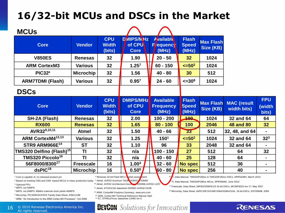
16/32-bit MCUs and DSCs in the Market
Core Vendor
CPU
Width
(bits)
DMIPS/MHz
of CPU
Core
Available
Frequency
(MHz)
Flash
Speed
(MHz)
Max Flash
Size (KB)
V850ES Renesas 32 1.90 20 - 50 32 1024
ARM CortexM3 Various 32 1.257 60 - 150 <=502 1024
PIC326 Microchip 32 1.56 40 - 80 30 512
ARM7TDMI (Flash) Various 32 0.957 24 - 60 <=308 1024
MCUs
3 Optional FPU 4 MIPS, not DMIPS 5 MIPS, not DMIPS. 80MHz external clock yields 40MIPS
DSCs
1 Core is capable of, no released product yet
2 Based on existing CM3 and CM4 -based MCUs in mass production today
6 Microchip. PIC32MX3XX/4XX Family Data Sheet, DS61143E
7 ARM, “An Introduction to the ARM Cortex-M3 Processor”, Oct 2006
8 Renesas 32-bit Flash MCU market assessment
9 Atmel, AVR32 brochure 7919F-AVR32-07/09/5K 10 Atmel, AVR32 Architecture Document 32000B-AVR32-11/07
11 Atmel, AT32UC3A datasheet 32058G-AVR32-01/09
12 ARM, CortexM4 Features Summary, www.arm.com 13 ARM, Cortex-M4 Technical Reference Manual r0p0 14 ST, STR91xFAxxx datasheet 13495 rev 6
15 TI, Data Manual, TMS320F283xx & TMS320F282xx DSCs, SPRS439H, March 2010
17 Freescale, Data Sheet, 56F8323/56F8123 16-bit DSCs, MC56F8323 rev 17, May 2007
18 Microchip, Data Sheet, dsPIC33FJXXXMCX06A/X08A/X10A, 16-bit DSCs, DS70594B, 2009
16 TI, Data Manual, TMS320F280xx MCus, SPRS584D, June 2010
Core Vendor
CPU
Width
(bits)
DMIPS/MHz
of CPU
Core
Available
Frequency
(MHz)
Flash
Speed
(MHz)
Max Flash
Size (KB)
MAC (result
width bits)
FPU
(width
bits)
SH-2A (Flash) Renesas 32 2.00 100 - 200 100 1024 32 and 64 64
RX600 Renesas 32 1.65 80 - 100 100 2046 48 and 80 32
AVR329,10,11 Atmel 32 1.50 40 - 66 33 512 32, 48, and 64 -
ARM CortexM412,13 Various 32 1.25 1501 <=502 1024 32 and 64 323
STR9 ARM966E14 ST 32 1.10 96 33 2048 32 and 64 -
TMS320 Delfino (Flash)15 TI 32 n/a 100 - 150 27 512 64 32
TMS320 Piccolo16 TI 32 n/a 40 - 60 25 128 64 -
56F8000/830017 Freescale 16 1.004 32 - 60 No spec 512 36 -
dsPIC18 Microchip 16 0.505 60 - 80 No spec 256 40 -

17 © 2010 Renesas Electronics America Inc. All rights reserved.
RX is Best of Both
Mem-to-Mem instructions
73 Inst + DSP + FPU
10 addressing modes
1 to 8 byte instructions
Up to 28% smaller code
• Any inst accesses memory
• Many rich instructions
• Many addressing modes
• Variable instruction formats
• Smaller code size in memory
• Single register set
• Multi-clock instructions
• Less to no pipelining
• Longer interrupt response
• Only load/store mem access
• Few instructions
• Few addressing modes
• Fixed instruction formats
• Larger code size in memory
• Multiple register sets
• Single-clock instructions
• Highly pipelined
• Faster interrupt response
CISC and RISC
16 x 32-bit registers
One clock per instruction
5-stage pipeline
5-clock interrupt response
Plus it has an FPU.
Let’s Build an RX…
Traditional CISC Complex Instruction Set Computer
GOAL: Small Memory Footprint
Traditional RISC Reduced Instruction Set Computer
GOAL: 1 Clock per Instruction
18 © 2010 Renesas Electronics America Inc. All rights reserved.
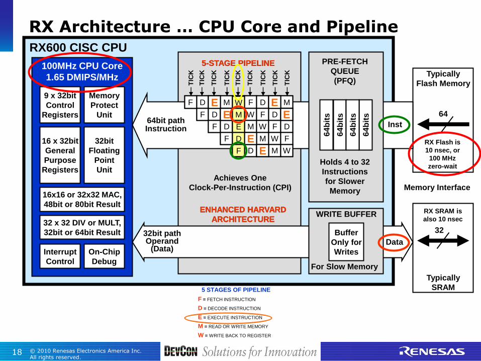
Typically
SRAM
Typically
Flash Memory
RX Flash is
10 nsec, or
100 MHz
zero-wait
RX SRAM is
also 10 nsec
RX600 CISC CPU
5-STAGE PIPELINE
5 STAGES OF PIPELINE
F = FETCH INSTRUCTION
D = DECODE INSTRUCTION
E = EXECUTE INSTRUCTION
M = READ OR WRITE MEMORY
W = WRITE BACK TO REGISTER
Inst 64bit path Instruction
Data 32bit path Operand
(Data)
ENHANCED HARVARD
ARCHITECTURE WRITE BUFFER
For Slow Memory
PRE-FETCH
QUEUE
(PFQ)
Holds 4 to 32
Instructions
for Slower
Memory Memory Interface
64
32
100MHz CPU Core
1.65 DMIPS/MHz
16 x 32bit
General
Purpose
Registers
9 x 32bit
Control
Registers
RX Architecture … CPU Core and Pipeline
32bit
Floating
Point
Unit
16x16 or 32x32 MAC,
48bit or 80bit Result
32 x 32 DIV or MULT,
32bit or 64bit Result
Memory
Protect
Unit
Interrupt
Control
On-Chip
Debug
ENHANCED HARVARD
ARCHITECTURE
5-STAGE PIPELINE
64
bit
s
64
bit
s
64
bit
s
64
bit
s
Buffer
Only for
Writes
F D E M W
TIC
K
F D
F
TIC
K
E
D
F
TIC
K
M
E
D
F
TIC
K
W
M
E
D
F
TIC
K
F
W
M
E
D
TIC
K
D
F
W
M
E
TIC
K
E
D
F
W
M
TIC
K
M
E
D
F
W
TIC
K
E E
E E
E
W
M
E
D
F
Achieves One
Clock-Per-Instruction (CPI)
E E

19 © 2010 Renesas Electronics America Inc. All rights reserved.
RX Architecture … Memory Interface
SRAM,
100MHz Access
64 bits
Flash Memory,
100MHz Access
64 bits
100 MHz Flash and SRAM means
zero wait-state code and data access
PFQ minimizes stalls from slower
memory, such as external memory
Bus master of Internal Bus 1 is the CPU
Next we look at Internal Bus 2…
External
Bus Pins
for CPU
External
Bus
Controller
(BSC)
32 bits
Internal Main Bus 1 32 bits
32 bits
Bus Bridge
Peripherals
RX600 MCU
RX600
CPU
100MHz
PIPELINE PFQ
BUFFER
64b INST
32b DATA
Bus Master of Internal Main Bus 1
BUS MATRIX

20 © 2010 Renesas Electronics America Inc. All rights reserved.
CNTL
Communication (USB, CAN, SCI, SPI, I2C)
Timers (MTU, TPU, TMR, CMT)
Analog (DAC, ADC, PGA)
GPIO
System Control (DMA, E2P, ICU, LVD,
RTC, WDG, CLKS)
Multiple Peripheral Busses to Spread Bandwidth Loading
CN
TL
CN
TL
CN
TL
Internal Main Bus 2 32 bits
DTC (bus master)
Bus Bridge
DMAC (bus master)
Ethernet DMAC (bus master)
RX Architecture … System Interface
RX600
CPU
100MHz
PIPELINE PFQ
BUFFER
64b INST
32b DATA
External
Bus Pins
for CPU
Bus Master of Internal Main Bus 1
64 bits
64 bits
Bus Bridge
EXDMA (external bus master)
32 bits
Internal Main Bus 1 32 bits
32 bits
RX600 MCU
BUS MATRIX
SRAM,
100MHz Access
Flash Memory,
100MHz Access
External
Bus
Controller
(BSC)
On
e E
xte
rnal D
ev
ice
A
no
ther
Exte
rnal D
ev
ice
Ethernet MAC
2K
FIFO
FIFO
2K

21 © 2010 Renesas Electronics America Inc. All rights reserved.
1.5
DMIPS per MHz
1.0
RX 1.65 DMIPS/MHz
Note: Dhrystone 2.1 numbers for ARM processors taken from www.arm.com
ARM7
ARM9
Cortex-M3
Cortex-M4
RX CPU Core Performance

22 © 2010 Renesas Electronics America Inc. All rights reserved.
Up to 43% Power Reduction
Low power design techniques
• Clock gating
• Low power HVT transistors in slower paths
• Power gating
Low power modes
• 500mA* per MHz in Run Mode
• All Peripherals ON
• Four Low-Power Modes
• Sleep
• All-Module Stop
• Standby
• Deep Standby
•2.5mA* in Deep Standby
• RX63x, RTC ON
Milliwatts* per DMIPS
2.0 1.0
43% less
= RX600
Note: Derived from IDD specifications stated in product datasheets
= A Cortex-M3 based MCU
* Typical Conditions, 3.3V and 25oC, all peripheral clocks on

23 © 2010 Renesas Electronics America Inc. All rights reserved.
RX600 Instruction Set
= Single clock instruction

24 © 2010 Renesas Electronics America Inc. All rights reserved.
Instruction Length (bytes)
List of Instructions Number of Instructions
1 NOP, RTS, BRK 3
1-3 BCnd 1
1-4 BRA 1
2 RMPA, ROLC, RORC, SAT, SATR, POP, POPC, POPM, PUSHC, PUSHM, JMP, JSR, SCMPU, SMOVB, SMOVF, SMOVU, SSTR, SUNTIL, SWHILE, CLRPSW, RTE, RTFI, SETPSW, WAIT
24
2-3 ABS, NEG, NOT, SHAR, SHLL, SHLR, RTSD 7
2-4 MOVU, PUSH, BSR 3
2-5 SUB, BCLR, BSET, BTST 4
2-6 ADD, AND, CMP, MUL, OR 5
2-8 MOV 1
3 ROTL, ROTR, REVL, REVW, INT, MVFC, MACHI, MACLO, MULHI, MULLO, MVFACHI, MVFACMI, MVTACHI, MVTACLO, RACW
15
3-5 FTOI, ROUND, SCCnd, BMCnd, BNOT 5
3-6 SBB, ITOF, XCHG 3
3-7 DIV, DIVU, EMUL, EMULU, MAX, MIN, TST, XOR, FADD, FCMP, FDIV, FMUL, FSUB, MVTC
14
4-6 ADC 1
4-7 STNZ, STZ 2
6% have
minimum
instruction length
of 1 byte
49% have
minimum
instruction length
of 2 bytes
42% have
minimum
instruction length
of 3 bytes
Total = 89 instructions MOV instruction length is 2-8 bytes
RX Instruction Set Summary and Size

25 © 2010 Renesas Electronics America Inc. All rights reserved.
Instruction length (bytes)
1 4 7 3 2 5 8 6
MOV instruction example
Rd opcode MEMMEM [Rs] [Rd] Rs
Function Source Destination
Rd Rs opcode MEMREG [Rs] Rd
Rd Rs opcode REGMEM Rs [Rd]
#IMM:8 Rd opcode #IMM:8 [Rd]
Rd opcode #IMM:16 #IMM:16 [Rd]
Rd Rs opcode REGREG Rs Rd
opcode Rd #IMM:32 IMMREG #IMM:32 Rd
opcode Rd #IMM:32 #IMM:32 [Rd]
IMMMEM
Rd #IMM:32 dsp:16 opcode #IMM:32 dsp:16[Rd]
Direct Memory-to-Memory operation

26 © 2010 Renesas Electronics America Inc. All rights reserved.
Example: Moving data in memory
Direct Memory-to-Memory operation allows RX to avoid lengthy load/store operations and results in smaller code size
MOV [r1], [r2]
RX
Code size = 2 bytes
Number of Cycles = 3
2 bytes LDR r3, [r1]
STR r3, [r2] 2 bytes
Traditional RISC
Code size = 4 bytes
Number of Cycles = 4
2 bytes

27 © 2010 Renesas Electronics America Inc. All rights reserved.
Up to 28% Code Size Reduction
Code size (relative)
1.0
28% less
= RX600
= A Cortex-M3 based MCU
19% less
17% less
25% less
25% less
Note: Internal benchmark test, your results may vary
Motor control
Data communication
Data conversion
Real-time control
System control

28 © 2010 Renesas Electronics America Inc. All rights reserved.
RX makes Out-of-Order Instruction Decisions
F D E M M WB
F D S S WB E
F D S S WB E
1) MOV [R1], R2
2) ADD R4, R5
3) SUB R4, R5
Instructions
Instructions 2) and 3) delayed, waiting on 1)
WB E
D WB E
F D E M M WB
F D
F
1) MOV [R1], R2
2) ADD R4, R5
3) SUB R4, R5
Delay is Eliminated
S S
S S
• Is possible when there are no dependencies
• Multiple WB within same clock cycle OK if destination is different
CPU Clock
Fetch
Decode
Execute
Memory
Write Back
Stall

29 © 2010 Renesas Electronics America Inc. All rights reserved.
Resolve Interrupt,
PC & PSW to Backup Regs
PC&PSW from B/U
Regs, Return
Optional
Push Gen
Regs to Stack
ISR
Optional Pop
Gen Regs
from Stack
RX Fast Interrupt
5 clks typ. 3 clks
Interrupt Handling IRQ
RX Normal Interrupt
7clks typ.
Resolve
Interrupt
PC & PSW
to Stack
Ret-
urn
POP PC & PSW from
Stack
Optional
Push Gen
Regs to Stack
ISR
Optional Pop
Gen Regs
from Stack
6 clks
Resolve Interrupt,
PC & PSW to Backup Regs
Return ISR
5 clks typ. 3 clks
RX Fast Interrupt plus Gen Register Usage
General CPU
Registers
R0 R1 R2 R3 R4 R5 R6 R7 R8 R9
R10 R11 R12 R13 R14 R15
= Automatic by CPU = Done by Firmware
Save 5 clocks
Save many clocks
* ARM, Technical Reference Manuals: CortexM3 r1p1, CortexM4 r0p0

30 © 2010 Renesas Electronics America Inc. All rights reserved.
Interrupt Handling IRQ
Resolve Interrupt,
PC & PSW to Backup Regs
Return ISR
5 clks typ. 3 clks
RX Fast Interrupt plus Gen Register Usage
Resolve Interrupt,
PC & PSW to Backup Regs
PC&PSW from B/U
Regs, Return
Optional
Push Gen
Regs to Stack
ISR
Optional Pop
Gen Regs
from Stack
RX Fast Interrupt
5 clks typ. 3 clks
= Automatic by CPU = Done by Firmware
Resolve Interrupt,
and Push CPU State
and 5 Regs to Stack
Pop CPU State and 5 regs
from Stack, and Return ISR
12 clks 12 clks
ARM Cortex M3 or M4*
* ARM, Technical Reference Manuals: CortexM3 r1p1, CortexM4 r0p0
Save up to 16 clocks
RX Typical Interrupt
7clks typ.
Resolve
Interrupt
PC & PSW
to Stack
Ret-
urn
POP PC & PSW from
Stack
Optional
Push Gen
Regs to Stack
ISR
Optional Pop
Gen Regs
from Stack
6 clks

31 © 2010 Renesas Electronics America Inc. All rights reserved.
Floating-Point Unit
Dedicated Data Registers
General Registers
Typical Operation
Load/Store
No Load/Store Instructions Needed
RX Operation
General Registers
Floating-Point Unit
FPU directly accesses General Registers
Higher FPU performance
Smaller code size

32 © 2010 Renesas Electronics America Inc. All rights reserved.
FPU Applications
© 2010 Renesas Electronics America Inc. All rights reserved. 32
Pressure regulator
Pump control
Thermo couple conversion
Motion Control
Motor Control
Flow Control
Digital filtering

33 © 2010 Renesas Electronics America Inc. All rights reserved.
FPU benefits: Two examples
© 2010 Renesas Electronics America Inc. All rights reserved. 33
1- Motor Control
FPU removes limitations due to scaling or saturation
Improves accuracy for motor position and speed
Increases motor efficiency
Easy code development and maintenance. Write formulas directly into C code
Reduces CPU loading
Reduces code size
2- Thermocouple Conversion
0
100
200
300
400
500
Look Up
Table
Fixed Point
Math
Software
Library
FPU
Size in Byte
Sensorless vector motor control compiled for
Fixed Integer vs Floating Point FPU
FPU provides the best combined execution time and code size

34 © 2010 Renesas Electronics America Inc. All rights reserved.
FPU Comparison
The FPU provides a dramatic increase in performance and code efficiency over math libraries.
Example: Conversion of thermocouple reading to temperature
Thermocouple formula: Temperature = S (an * xn)
n = 0 ~ 5; a0 ~ a5 are constants; x is A/D reading
MCU Operating Frequency
(MHZ)
CPU Cycles (count)
Actual Execution
Time (usec)
Execution Time with
Ideal Memory (usec)
Code Size (bytes)
RX600 100 94 0.94 0.94 48
A CM3-based MCU
72 1130 15.7 14.7 892
> 16x
Faster > 18x
Smaller
• RX610 MCU: Renesas Compiler v0.02 Alpha, Size Max
• A CM3-based MCU: IAR Compiler v4.42A, Size Max

35 © 2010 Renesas Electronics America Inc. All rights reserved.
DSP Arithmetic Functions
Repeated Multiply and Accumulate (RMPA)
16-bit
16-bit
General register
General register 48-bit
Multiply-Accumulate unit
Multiply and Accumulate (MAC)
Memory (coeffic-ients)
32-bit
32-bit
80-bit
Multiply-Accumulate unit
Memory (ADC
Samples) Accumulate Accumulate Accumulate Accumulate Accumulate Accumulate Accumulate

36 © 2010 Renesas Electronics America Inc. All rights reserved.
60 MHz
2 wait cycles
IF D E M WBIF D E M WB
IF D E M WBIF D E M WB
1 wait cycle
IF D E M WBIF D E M WB
IF D E M WBIF D E M WB
30 MHz
no wait
IF D E M WBIF D E M WB
IF D E M WBIF D E M WB
D E M WBD E M WB
D E M WBD E M WB
W
W
D E M WBD E M WB
D E M WBD E M WBW
W W
W
100 MHz
Pro
cessin
g p
erf
orm
ance
MCU
frequency
RX with 100 MHz
Flash
Competing MCU with 30 MHz
Flash
Performance and Flash Speed

37 © 2010 Renesas Electronics America Inc. All rights reserved.
FIR Filter, RX600 and a CM3-based MCU
0.000
0.500
1.000
1.500
2.000
2.500
3.000
3.500
4.000
4.500
5.000
16 24 32 40 48 56 64 72 80 88 96 100
MCU Operating Frequency (MHz)
Co
mp
leti
on
Tim
e,
10
0 i
tera
tio
ns
of
FIR
Alg
ori
thm
(u
se
c)
A CM3 MCU Theorectical (73 CPU cycles per Iteration)
A CM3 MCU Actual w/ Memory Acceleration
A CM3 MCU Actual w/o Memory Acceleration
RX600 Theorectical (46 CPU cycles per Iteration)
RX600 Actual
DSP and Benefit of 10nsec Flash
• Theoretical performance with “No-Wait Memory” for this CM3 MCU
• Performance loss due to Flash slower than CPU demand on a CM3 MCU
• Mitigation effect of Memory Acceleration on a CM3 MCU
• Theoretical performance with “No-Wait Memory” for RX600
• Theoretical is Identical to Actual performance for RX600 because of 10nsec Flash
• 8 Tap FIR Filter, 16 x 16 to 32bit accumulate
• RX610 MCU: Renesas compiler v1.0, Speed 2, macro used for RMPA
• A CM3-based MCU: IAR Compiler v5.40.0.315, Speed Max
Lower
is
Better
1 wait
state
2 wait
states
Better, but
delay
remains
RX has 63%
better
performance
8 Tap FIR Filter
16 x 16 to 32-bit accumulate

38 © 2010 Renesas Electronics America Inc. All rights reserved.
Flash-MCU History and Speed
1990 2000 2010 Year
Op
era
tin
g F
req
uen
cy (
MH
z)
100
10
2005 1995
Competitors
(0.15um) (90nm)
(40nm)
(0.8um)
(0.5um)
(0.35um)
(0.18um)
Flash-MONOS
MONOS for EEPROM & IC-card
MCU Freq.
Renesas Flash Freq.
General Flash Freq.
Renesas MONOS reaches
100MHz single cycle access
Source: Renesas

39 © 2010 Renesas Electronics America Inc. All rights reserved.
50
Max MHz
100
200
2010Existing MCUs 2011 2012
FamilyFamily
RX600 SeriesRX600 Series32 Bit, 90nm32 Bit, 90nm
Extreme High PerformanceExtreme High Performance
High EfficiencyHigh Efficiency
RX200 SeriesRX200 Series32 Bit, 130 nm32 Bit, 130 nm
High PerformanceHigh Performance
Low Power / Low VoltageLow Power / Low Voltage
RX600RX60040 nm40 nm100MHz+100MHz+
H8SXH8SX32 Bit32 Bit
R32CR32C32 Bit32 Bit
M16CM16C16 Bit16 Bit
H8SH8S16 Bit16 Bit
RX Family Roadmap

40 © 2010 Renesas Electronics America Inc. All rights reserved.
RX600 System On A Chip
41 © 2010 Renesas Electronics America Inc. All rights reserved.
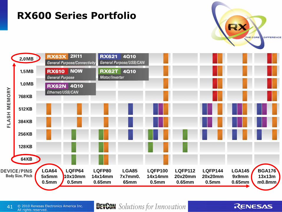
RX600 Series Portfolio
LGA64
5x5mm
0.5mm
LQFP64
10x10mm
0.5mm
LQFP80
14x14mm
0.65mm
LGA85
7x7mm0.
65mm
LQFP100
14x14mm
0.5mm
LQFP112
20x20mm
0.65mm
LQFP144
20x20mm
0.5mm
LGA145
9x9mm
0.65mm
BGA176
13x13m
m0.8mm

42 © 2010 Renesas Electronics America Inc. All rights reserved.
RX600 Series - 100Mhz Extreme Performance
RX Migration Between Series
Pins
Flash
32 176
32KB
2MB
RX200 Series - 50Mhz Low Power / Low Voltage
RX600: 500uA/MHz (all peripherals on), 2.5uA RTC Deep Standby, 2.7V to 3.6V
RX200: 200uA/MHz (all peripherals on), <1uA RTC Deep Standby, 1.62V to 3.6V
Common CPU & Peripherals
48 64 80/85 100 112 144/145
1MB
64KB
128KB
256KB
384KB
512KB
Migration
Within RX
Family

43 © 2010 Renesas Electronics America Inc. All rights reserved.
RX Solutions
Motor Control, RX62T
Drive Sensorless PMAC Motor
Field Oriented Control, 3-phase
High integration, low system cost
Direct Drive TFT-LCD, RX62N
Drive 4.3” Color WQVGA TFT-LCD by RGB
Full basic graphic library and demo
Source code included
WiFi
802.11b/g/n WiFi, RX62N
Simple SPI connection to WiFi module
Kit contains driver and examples
Very low power 802.11b/g/n connectivity
Connectivity, RX62N RDK
Ethernet, USB Host/Device/USB, CAN
Many surrounding functions/features
Source code, built-in JTAG debugger
See www.am.renesas.com/rx for details

44 © 2010 Renesas Electronics America Inc. All rights reserved.
RX Tools for Solutions See www.am.renesas.com/rx for details
Hi-Speed Trace • JTAG, USB-HS, plus 6 lines connection • Trace depth: - 2M branches/cycles • SRAM monitor, 4 KB
On-Chip Debug • JTAG and USB-HS connection • Program Flash • Single step execution • 256 Software break points • 12 Hardware breakpoints • PC and data breakpoints • On-chip Trace - 256 branches/cycles • Read/Write SRAM • Read/Write C variables • Performance monitoring • Non-intrusive • Hot-plug capable
E1
E20
$99*
$995*
HEW4 Plus Renesas C/C++ $1200*
Single Integrated Development & Debugging Environment
HEW4 also supports GNU-RX C/C++ compiler, all at $0
Wide 3rd Party Support for IDE, Compilers, Middleware, RTOS:
• Micrium, IAR, Segger, CMX, KPIT Cummings, freeRTOS, and more
* Suggested resale price when sold individually

45 © 2010 Renesas Electronics America Inc. All rights reserved.
Feature Unit RX600 CortexM31 CortexM42 AVR32A3 PIC324
CPU Type - CISC, DSC RISC, MCU RISC, DSC RISC, DSC RISC, MCU
Performance DMIPS/MHz 1.65 1.25 1.25 1.50 1.50
Pipeline Length Stages 5 3 3 3 5
Inst Lengths Bytes 1 to 8 2 and 4 2 and 4 2 and 4 2 and 4
# of Instructions For CPU,DSP 80, 9 97,3 97,83 115,8 129, 2
FPU # of instructions Yes, 8 No, 0 Option, 25 No, 0 No, 0
General Regs # of regs, bits 15 x 32 12 x 32 12 x 32 13 x 32 27 x 32
Min Intr Latency CPU Clocks 7 or 5 12 or 6 12 or 6 12 or 2 12 instructions
MPU - Option Option Option Option No
Bit Manipulation - Yes Yes Yes Yes Yes
Debug Connection JTAG or
2-wire
JTAG or
2-wire
JTAG or
2-wire JTAG JTAG
Hi-Speed Trace Connection 6-wire 6-wire 6-wire 12-wire 4,8,or 16-wire
Comparing other 32-bit CPU Architectures
1 ARM, CortexM3 Technical Reference Manual Revision:r1p1, ARMv7-M Architecture Reference Manual DDI 0403C_errata_v3 2 ARM, CortexM4 Technical Reference Manual Revision:r0p0, ARMv7-M Architecture Reference Manual DDI 0403C_errata_v3 3 Atmel, AVR32C Technical Reference Manual 32002A-AVR32-03/07 4 Microchip, PIC32MX Family Reference Manual DS611271C. MIPS Technology, MIPS32 Architecture for Programmers Vol II: MIPS32 Instruction Set, rev 2.5, MIPS32 MK4 Processor Core Datasheet, Rev 02.01
References:

46 © 2010 Renesas Electronics America Inc. All rights reserved.
Who’s the Best? You Decide based on what you have seen.
To help your decision, here are publicly released benchmark results based on widely acknowledged CoremarkTM from EEMBC.
*Vendor *Processor Type *CPU Freq (MHz)
*CoreMark / MHz
*CoreMark *Compiler Comment
Microchip PIC32MX360F512L MCU 30 2.599 78 GCC 4.3.2 Only 30 MHz operation
Microchip PIC32MX360F512L MCU 80 2.297 184 GCC 4.3.2 Negative effect of slow
Flash
Renesas RX610 DSC 100 2.240 224 GNURX 201009
Full speed with no loss of performance
TI Stellaris LM3S9B96
CortexM3 MCU 50 1.921 96
Keil V4.0.0.524
ST STM32 CortexM3
120MHz. 90nm MCU 120 1.905 229
KEIL 4.0.0.524
Has new “ART” memory accelerator
Microchip PIC24HJ128GP202 MCU 40 1.862 74 GCC4.0.3
ST STM32F103RB
CortexM3 MCU 24 1.797 43 GCC 4.4.1
NXP LPC1768 MCU 100 1.753 175 ARMCC 4.0
TI Stellaris LM3S9B96
CortexM3 MCU 80 1.596 127
Keil V4.0.0.524
Negative effect of slow Flash
ST STM32F103RB
CortexM3 MCU 72 1.504 108 GCC 4.4.1
Negative effect of slow Flash
Freescale ColdFire MCF52233 MCU 60 1.038 62 IAR EW 1.20
Freescale ColdFire MCF5274 MCU 150 0.773 115 GCC4.1.1
*Source: www.coremark.org as of 1 Sep 2010
Sorted by
CoreMark/MHz

47 © 2010 Renesas Electronics America Inc. All rights reserved.
Who’s the Best? Now sorted by raw Coremark, not Coremark/MHz
*Vendor *Processor Type *CPU Freq (MHz)
*CoreMark / MHz
*CoreMark *Compiler Comment
ST STM32 CortexM3
120MHz. 90nm MCU 120 1.905 229
KEIL 4.0.0.524
Much Higher CPU freq needed for same result
Renesas RX610 DSC 100 2.240 224 GNURX 201009
Positive effect of efficient CPU and fast Flash
Microchip PIC32MX360F512L MCU 80 2.297 184 GCC 4.3.2
NXP LPC1768 MCU 100 1.753 175 ARMCC 4.0
TI Stellaris LM3S9B96
CortexM3 MCU 80 1.596 127
Keil V4.0.0.524
Freescale ColdFire MCF5274 MCU 150 0.773 115 GCC4.1.1
ST STM32F103RB
CortexM3 MCU 72 1.504 108 GCC 4.4.1
TI Stellaris LM3S9B96
CortexM3 MCU 50 1.921 96
Keil V4.0.0.524
Microchip PIC32MX360F512L MCU 30 2.599 78 GCC 4.3.2
Microchip PIC24HJ128GP202 MCU 40 1.862 74 GCC4.0.3
Freescale ColdFire MCF52233 MCU 60 1.038 62 IAR EW 1.20
ST STM32F103RB
CortexM3 MCU 24 1.797 43 GCC 4.4.1
*Source: www.coremark.org as of 1 Sep 2010
Sorted by
CoreMark/MHz

48 © 2010 Renesas Electronics America Inc. All rights reserved.
Questions
1: What is the read access time of RX600 Flash Memory?
10 nsec (100MHz) across entire voltage range 2.7V to 3.6V
1.65 DMIPS/MHz, and 1mW/DMIPS
2: How many DMIPS/MHz does RX600 produce, and how many mW/DMIP does it consume?
3: What does the RMPA instruction do?
Repeat Multiply Accumulate. One instruction automatically multiplies data from
two different memory arrays, and adds result to 80-bit accumulator, then
post-increments to next two values. Repeats until specified array length is
met. DSP!!

49 © 2010 Renesas Electronics America Inc. All rights reserved.
Innovation – Single Chip Enablement
One MCU Family for many applications
See www.am.renesas.com/rx for details

50 © 2010 Renesas Electronics America Inc. All rights reserved.
Feedback Form
Please fill out the feedback form!
If you do not have one, please raise your hand
© 2010 Renesas Electronics America Inc. All rights reserved.
51
Thank You!
www.am.renesas.com/rx

Renesas Electronics America Inc.