ieee 802.3at poe high-power pd interface with external ... features 3 description the tps2379 device...
TRANSCRIPT
RTN
VC
VSS
CLS
DEN
CDB
T2P
GATE
TPS2379
SS
Q1
C1
D1
RDEN
RCLS
RBLST
VDDRT2P
CBULK
DC
/DC
Co
nv
ert
er
Fro
m E
the
rne
tTra
ns
form
ers
Fro
m S
pa
reP
air
s o
rTra
ns
form
ers
Product
Folder
Sample &Buy
Technical
Documents
Tools &
Software
Support &Community
ReferenceDesign
TPS2379SLVSB98A –MARCH 2012–REVISED JULY 2015
TPS2379 IEEE 802.3at PoE High-Power PD Interface With External Gate Driver1 Features 3 Description
The TPS2379 device is an 8-pin integrated circuit that1• IEEE 802.3at Type-2 Hardware Classification With
contains all of the features needed to implement anStatus FlagIEEE802.3at type-2 powered device (PD) such as
• Auxiliary Gate Driver for High-Power Expansion Detection, Classification, Type 2 Hardware• Robust 100-V, 0.5-Ω Hotswap MOSFET Classification, and 140-mA inrush current limit during
startup. The low 0.5-Ω internal switch resistance,• 1A (Typical) Operating Current Limitcombined with the enhanced thermal dissipation of• 140 mA (Typical) Inrush Current Limit the PowerPAD package, enables this controller to
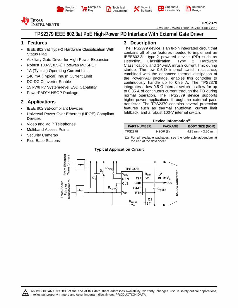
• DC-DC Converter Enable continuously handle up to 0.85 A. The TPS2379integrates a low 0.5-Ω internal switch to allow for up• 15 kV/8 kV System-level ESD Capabilityto 0.85 A of continuous current through the PD during• PowerPAD™ HSOP Package normal operation. The TPS2379 device supportshigher-power applications through an external pass2 Applications transistor. The TPS2379 contains several protectionfeatures such as thermal shutdown, current limit• IEEE 802.3at-compliant Devicesfoldback, and a robust 100-V internal switch.• Universal Power Over Ethernet (UPOE) Compliant
Devices Device Information(1)• Video and VoIP Telephones PART NUMBER PACKAGE BODY SIZE (NOM)• Multiband Access Points TPS2379 HSOP (8) 4.89 mm × 3.90 mm• Security Cameras
(1) For all available packages, see the orderable addendum at• Pico-Base Stations the end of the data sheet.
Typical Application Circuit
1
An IMPORTANT NOTICE at the end of this data sheet addresses availability, warranty, changes, use in safety-critical applications,intellectual property matters and other important disclaimers. PRODUCTION DATA.
TPS2379SLVSB98A –MARCH 2012–REVISED JULY 2015 www.ti.com
Table of Contents8.4 Device Functional Modes........................................ 141 Features .................................................................. 1
9 Application and Implementation ........................ 222 Applications ........................................................... 19.1 Application Information............................................ 223 Description ............................................................. 19.2 Typical Application .................................................. 224 Revision History..................................................... 2
10 Power Supply Recommendations ..................... 255 Pin Configuration and Functions ......................... 311 Layout................................................................... 256 Specifications......................................................... 4
11.1 Layout Guidelines ................................................. 256.1 Absolute Maximum Ratings ...................................... 411.2 Layout Example .................................................... 266.2 ESD Ratings.............................................................. 411.3 Thermal Considerations and OTSD...................... 286.3 Recommended Operating Conditions....................... 411.4 ESD....................................................................... 286.4 Thermal Information .................................................. 5
12 Device and Documentation Support ................. 296.5 Electrical Characteristics........................................... 512.1 Documentation Support ........................................ 296.6 Typical Characteristics .............................................. 712.2 Community Resources.......................................... 297 Parameter Measurement Information .................. 912.3 Trademarks ........................................................... 298 Detailed Description ............................................ 1012.4 Electrostatic Discharge Caution............................ 298.1 Overview ................................................................. 1012.5 Glossary ................................................................ 298.2 Functional Block Diagram ....................................... 10
13 Mechanical, Packaging, and Orderable8.3 Feature Description................................................. 10Information ........................................................... 29
4 Revision HistoryNOTE: Page numbers for previous revisions may differ from page numbers in the current version.
Changes from Original (March 2012) to Revision A Page
• Added ESD Ratings table, Feature Description section, Device Functional Modes, Application and Implementationsection, Power Supply Recommendations section, Layout section, Device and Documentation Support section, andMechanical, Packaging, and Orderable Information section ................................................................................................. 1
• Deleted Classification Resistor, RCLS section..................................................................................................................... 13• Deleted CDB Pin Interface section....................................................................................................................................... 13• Deleted GATE Pin Interface section .................................................................................................................................... 13• Deleted External Boost Circuit (Q1, Q2, and RBLST) Considerations section ....................................................................... 13• Deleted T2P Pin Interface ................................................................................................................................................... 13• Deleted Detailed Pin Descriptions section .......................................................................................................................... 21
2 Submit Documentation Feedback Copyright © 2012–2015, Texas Instruments Incorporated
Product Folder Links: TPS2379
1
3
2
4
6
5
7
8
DEN
CLS
VDD
VSS
T2P
CDB
RTN
GATE
TPS2379www.ti.com SLVSB98A –MARCH 2012–REVISED JULY 2015
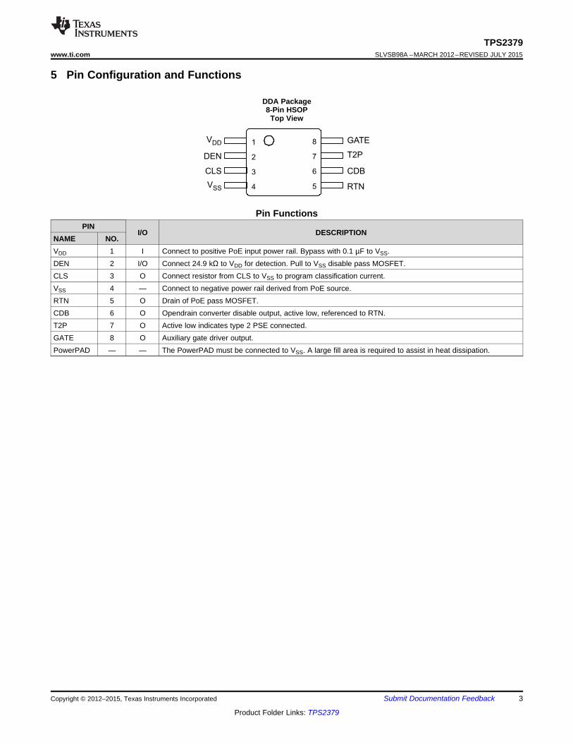
5 Pin Configuration and Functions
DDA Package8-Pin HSOP
Top View
Pin FunctionsPIN
I/O DESCRIPTIONNAME NO.VDD 1 I Connect to positive PoE input power rail. Bypass with 0.1 µF to VSS.DEN 2 I/O Connect 24.9 kΩ to VDD for detection. Pull to VSS disable pass MOSFET.CLS 3 O Connect resistor from CLS to VSS to program classification current.VSS 4 — Connect to negative power rail derived from PoE source.RTN 5 O Drain of PoE pass MOSFET.CDB 6 O Opendrain converter disable output, active low, referenced to RTN.T2P 7 O Active low indicates type 2 PSE connected.GATE 8 O Auxiliary gate driver output.PowerPAD — — The PowerPAD must be connected to VSS. A large fill area is required to assist in heat dissipation.
Copyright © 2012–2015, Texas Instruments Incorporated Submit Documentation Feedback 3
Product Folder Links: TPS2379
TPS2379SLVSB98A –MARCH 2012–REVISED JULY 2015 www.ti.com
6 Specifications
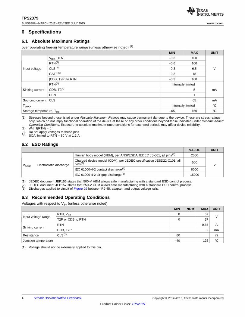
6.1 Absolute Maximum Ratingsover operating free-air temperature range (unless otherwise noted) (1)
MIN MAX UNITVDD, DEN –0.3 100RTN (2) –0.6 100
Input voltage CLS (3) –0.3 6.5 VGATE (3) –0.3 18[CDB, T2P] to RTN –0.3 100RTN (4) Internally limited
Sinking current CDB, T2P 5 mADEN 1
Sourcing current CLS 65 mATJMAX Internally limited °CStorage temperature, Tstg –65 150 °C
(1) Stresses beyond those listed under Absolute Maximum Ratings may cause permanent damage to the device. These are stress ratingsonly, which do not imply functional operation of the device at these or any other conditions beyond those indicated under RecommendedOperating Conditions. Exposure to absolute-maximum-rated conditions for extended periods may affect device reliability.
(2) With I(RTN) = 0(3) Do not apply voltages to these pins(4) SOA limited to RTN = 80 V at 1.2 A.
6.2 ESD RatingsVALUE UNIT
Human body model (HBM), per ANSI/ESDA/JEDEC JS-001, all pins (1) 2000Charged device model (CDM), per JEDEC specification JESD22-C101, all 500pins (2)V(ESD) Electrostatic discharge VIEC 61000-4-2 contact discharge (3) 8000IEC 61000-4-2 air-gap discharge (3) 15000
(1) JEDEC document JEP155 states that 500-V HBM allows safe manufacturing with a standard ESD control process.(2) JEDEC document JEP157 states that 250-V CDM allows safe manufacturing with a standard ESD control process.(3) Discharges applied to circuit of Figure 26 between RJ-45, adapter, and output voltage rails.
6.3 Recommended Operating ConditionsVoltages with respect to VSS (unless otherwise noted)
MIN NOM MAX UNITRTN, VDD 0 57
Input voltage range VT2P or CDB to RTN 0 57RTN 0.85 A
Sinking currentCDB, T2P 2 mA
Resistance CLS (1) 60 ΩJunction temperature –40 125 °C
(1) Voltage should not be externally applied to this pin.
4 Submit Documentation Feedback Copyright © 2012–2015, Texas Instruments Incorporated
Product Folder Links: TPS2379
TPS2379www.ti.com SLVSB98A –MARCH 2012–REVISED JULY 2015
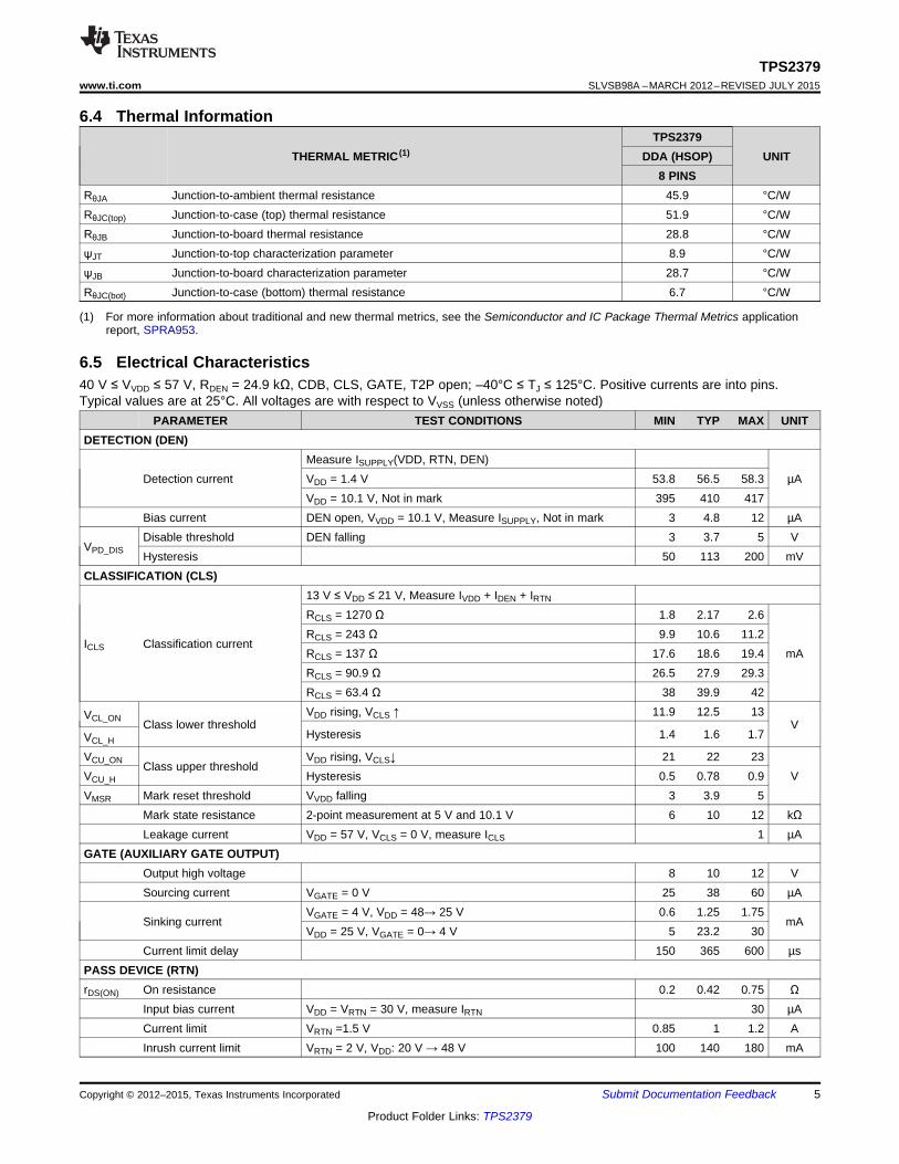
6.4 Thermal InformationTPS2379
THERMAL METRIC (1) DDA (HSOP) UNIT8 PINS
RθJA Junction-to-ambient thermal resistance 45.9 °C/WRθJC(top) Junction-to-case (top) thermal resistance 51.9 °C/WRθJB Junction-to-board thermal resistance 28.8 °C/WψJT Junction-to-top characterization parameter 8.9 °C/WψJB Junction-to-board characterization parameter 28.7 °C/WRθJC(bot) Junction-to-case (bottom) thermal resistance 6.7 °C/W
(1) For more information about traditional and new thermal metrics, see the Semiconductor and IC Package Thermal Metrics applicationreport, SPRA953.
6.5 Electrical Characteristics40 V ≤ VVDD ≤ 57 V, RDEN = 24.9 kΩ, CDB, CLS, GATE, T2P open; –40°C ≤ TJ ≤ 125°C. Positive currents are into pins.Typical values are at 25°C. All voltages are with respect to VVSS (unless otherwise noted)
PARAMETER TEST CONDITIONS MIN TYP MAX UNITDETECTION (DEN)
Measure ISUPPLY(VDD, RTN, DEN)Detection current VDD = 1.4 V 53.8 56.5 58.3 µA
VDD = 10.1 V, Not in mark 395 410 417Bias current DEN open, VVDD = 10.1 V, Measure ISUPPLY, Not in mark 3 4.8 12 µADisable threshold DEN falling 3 3.7 5 V
VPD_DIS Hysteresis 50 113 200 mVCLASSIFICATION (CLS)
13 V ≤ VDD ≤ 21 V, Measure IVDD + IDEN + IRTN
RCLS = 1270 Ω 1.8 2.17 2.6RCLS = 243 Ω 9.9 10.6 11.2
ICLS Classification currentRCLS = 137 Ω 17.6 18.6 19.4 mARCLS = 90.9 Ω 26.5 27.9 29.3RCLS = 63.4 Ω 38 39.9 42VDD rising, VCLS ↑ 11.9 12.5 13VCL_ON Class lower threshold VHysteresis 1.4 1.6 1.7VCL_H
VCU_ON VDD rising, VCLS↓ 21 22 23Class upper threshold
VCU_H Hysteresis 0.5 0.78 0.9 VVMSR Mark reset threshold VVDD falling 3 3.9 5
Mark state resistance 2-point measurement at 5 V and 10.1 V 6 10 12 kΩLeakage current VDD = 57 V, VCLS = 0 V, measure ICLS 1 µA
GATE (AUXILIARY GATE OUTPUT)Output high voltage 8 10 12 VSourcing current VGATE = 0 V 25 38 60 µA
VGATE = 4 V, VDD = 48→ 25 V 0.6 1.25 1.75Sinking current mA
VDD = 25 V, VGATE = 0→ 4 V 5 23.2 30Current limit delay 150 365 600 µs
PASS DEVICE (RTN)rDS(ON) On resistance 0.2 0.42 0.75 Ω
Input bias current VDD = VRTN = 30 V, measure IRTN 30 µACurrent limit VRTN =1.5 V 0.85 1 1.2 AInrush current limit VRTN = 2 V, VDD: 20 V → 48 V 100 140 180 mA
Copyright © 2012–2015, Texas Instruments Incorporated Submit Documentation Feedback 5
Product Folder Links: TPS2379
TPS2379SLVSB98A –MARCH 2012–REVISED JULY 2015 www.ti.com
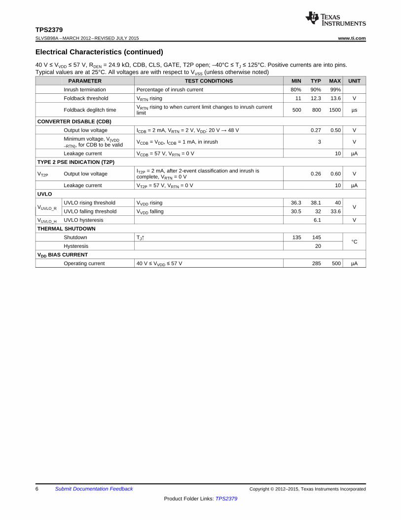
Electrical Characteristics (continued)40 V ≤ VVDD ≤ 57 V, RDEN = 24.9 kΩ, CDB, CLS, GATE, T2P open; –40°C ≤ TJ ≤ 125°C. Positive currents are into pins.Typical values are at 25°C. All voltages are with respect to VVSS (unless otherwise noted)
PARAMETER TEST CONDITIONS MIN TYP MAX UNITInrush termination Percentage of inrush current 80% 90% 99%Foldback threshold VRTN rising 11 12.3 13.6 V
VRTN rising to when current limit changes to inrush currentFoldback deglitch time 500 800 1500 µslimitCONVERTER DISABLE (CDB)
Output low voltage ICDB = 2 mA, VRTN = 2 V, VDD: 20 V → 48 V 0.27 0.50 VMinimum voltage, V(VDD VCDB = VDD, ICDB = 1 mA, in inrush 3 V–RTN), for CDB to be validLeakage current VCDB = 57 V, VRTN = 0 V 10 µA
TYPE 2 PSE INDICATION (T2P)IT2P = 2 mA, after 2-event classification and inrush isVT2P Output low voltage 0.26 0.60 Vcomplete, VRTN = 0 V
Leakage current VT2P = 57 V, VRTN = 0 V 10 µAUVLO
UVLO rising threshold VVDD rising 36.3 38.1 40VUVLO_R V
UVLO falling threshold VVDD falling 30.5 32 33.6VUVLO_H UVLO hysteresis 6.1 VTHERMAL SHUTDOWN
Shutdown TJ↑ 135 145°C
Hysteresis 20VDD BIAS CURRENT
Operating current 40 V ≤ VVDD ≤ 57 V 285 500 µA
6 Submit Documentation Feedback Copyright © 2012–2015, Texas Instruments Incorporated
Product Folder Links: TPS2379

120
160
200
240
280
320
360
400
20 25 30 35 40 45 50 55 60
TA = −40°C
TA = 125°CTA = 25°C
V(VDD−VSS) (V)
I VD
D (
µA)
G009
3
3.5
4
4.5
−50 −25 0 25 50 75 100 125
Mark Reset Threshold
Junction Temperature (°C)
V(V
DD
−VS
S) (
V)
G006
21
21.5
22
22.5
−50 −25 0 25 50 75 100 125
Class Upper Threshold, On
Class Upper Threshold, Off
Junction Temperature (°C)
V(V
DD
−VS
S) (
V)
G003
10.5
11
11.5
12
12.5
13
−50 −25 0 25 50 75 100 125
Class Lower Threshold, On
Class Lower Threshold, Off
Junction Temperature (°C)
V(V
DD
−VS
S) (
V)
G004
0
1
2
3
4
5
6
7
0 1 2 3 4 5 6 7 8 9 10
TA = −40°C
TA = 125°C
TA = 25°C
V(VDD−VSS) (V)
I VD
D (
µA)
G001
0
10
20
30
40
50
0 1 2 3 4 5 6 7 8 9 10
Detection Resistance
V(VDD−VSS) (V)
Res
ista
nce
(kΩ
)
G002
TPS2379www.ti.com SLVSB98A –MARCH 2012–REVISED JULY 2015
6.6 Typical Characteristics
Figure 1. Detection Bias Current vs PoE Voltage Figure 2. Detection Resistance vs PoE Voltage
Figure 3. Classification Upper Threshold vs Temperature Figure 4. Classification Lower Threshold vs Temperature
Figure 5. IVDD Bias Current vs Voltage Figure 6. Mark Reset Threshold vs Temperature
Copyright © 2012–2015, Texas Instruments Incorporated Submit Documentation Feedback 7
Product Folder Links: TPS2379

0.99
1
1.01
1.02
−50 −25 0 25 50 75 100 125Junction Temperature (°C)
Cur
rent
Lim
it (A
)
G011
38.2
38.22
38.24
38.26
38.28
38.3
−50 −25 0 25 50 75 100 125
UVLO Rising Threshold
Junction Temperature (°C)
V(V
DD
−VS
S) (
V)
G012
85
86
87
88
89
−50 −25 0 25 50 75 100 125
Junction Temperature (°C)
Inru
sh
Cu
rre
ntTe
rmin
atio
n
(%)
G010
120
130
140
150
160
−50 −25 0 25 50 75 100 125Junction Temperature (°C)
Cur
rent
Inru
sh L
imit
(mA
)
G009
8.5
8.8
9
9.2
9.5
9.8
10
−50 −25 0 25 50 75 100 125
Junction Temperature (°C)
Ma
rk R
esis
tan
ce
(k
)Ω
G007
0.2
0.3
0.4
0.5
0.6
0.7
−50 −25 0 25 50 75 100 125Junction Temperature (°C)
Pas
s F
ET
Res
ista
nce
(Ω)
G008
TPS2379SLVSB98A –MARCH 2012–REVISED JULY 2015 www.ti.com
Typical Characteristics (continued)
Figure 8. Pass FET Resistance vs TemperatureFigure 7. Mark Resistance vs Temperature
Figure 9. PoE Inrush Current Limit vs Temperature Figure 10. Inrush Termination Threshold vs Temperature
Figure 11. PoE Current Limit vs Temperature Figure 12. UVLO Rising Threshold vs Temperature
8 Submit Documentation Feedback Copyright © 2012–2015, Texas Instruments Incorporated
Product Folder Links: TPS2379
Idle Detect Class
Mark Class
Mark ClassBetweenRanges
Between
Ranges
Operating
T2Popen-drain
OperatingT2P low
Between
Ranges
UVLO
Rising
UVLO
Falling
UVLORising
UVLO
Falling
TYPE 2 PSE
Hardware Class
Class
TYPE 1 PSE
Hardware Class
Between
Ranges
PoE Startup Sequence
Detect
MarkReset
32.04
32.06
32.08
32.1
32.12
32.14
32.16
−50 −25 0 25 50 75 100 125
UVLO Falling Threshold
Junction Temperature (°C)
V(V
DD
−VS
S) (
V)
G013
9.6
9.7
9.8
9.9
10
−50 −25 0 25 50 75 100 125
Auxilary Gate Voltage
Junction Temperature (°C)
V(G
AT
E−V
SS
) (V
)
G015
TPS2379www.ti.com SLVSB98A –MARCH 2012–REVISED JULY 2015
Typical Characteristics (continued)
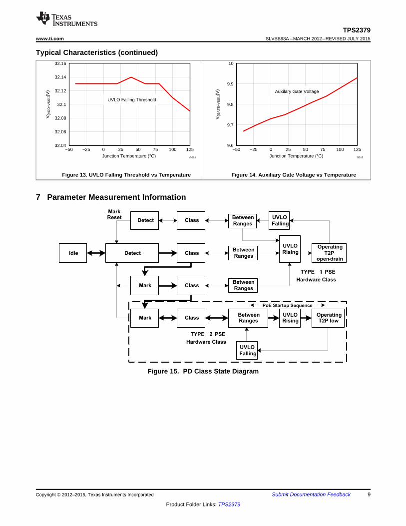
Figure 13. UVLO Falling Threshold vs Temperature Figure 14. Auxiliary Gate Voltage vs Temperature
7 Parameter Measurement Information
Figure 15. PD Class State Diagram
Copyright © 2012–2015, Texas Instruments Incorporated Submit Documentation Feedback 9
Product Folder Links: TPS2379
12V &10V
22V &21.25V
38.1V &32V
VDD
1
0
S
RQ
Inrush limit
threshold
Current limit
threshold
VSS RTN
CLS
VSS DEN
800ms
2.5VREG.
DetectionComp.
4V
HotswapMOSFET
ClassComp.
MarkComp. 12V
UVLOComp.
OTSD
IRTN sense,1 if < 90% of inrush current limit
1 = inrush
Signals referenced to VSS unless otherwise noted
1
4 5
3
2
ClassComp.
5V & 4V
0 = current limit
Inrush latch
800ms
1
0IRTN sense
RTN
Type 2State Eng.
Mark Comp Output
UVLO Comp Output
VSS
365ms
8 GATE
6V
GATE DRIVER
S
R
Q
RTN
High if over
temperauture
6CDB
7 T2P
RTN
TPS2379SLVSB98A –MARCH 2012–REVISED JULY 2015 www.ti.com
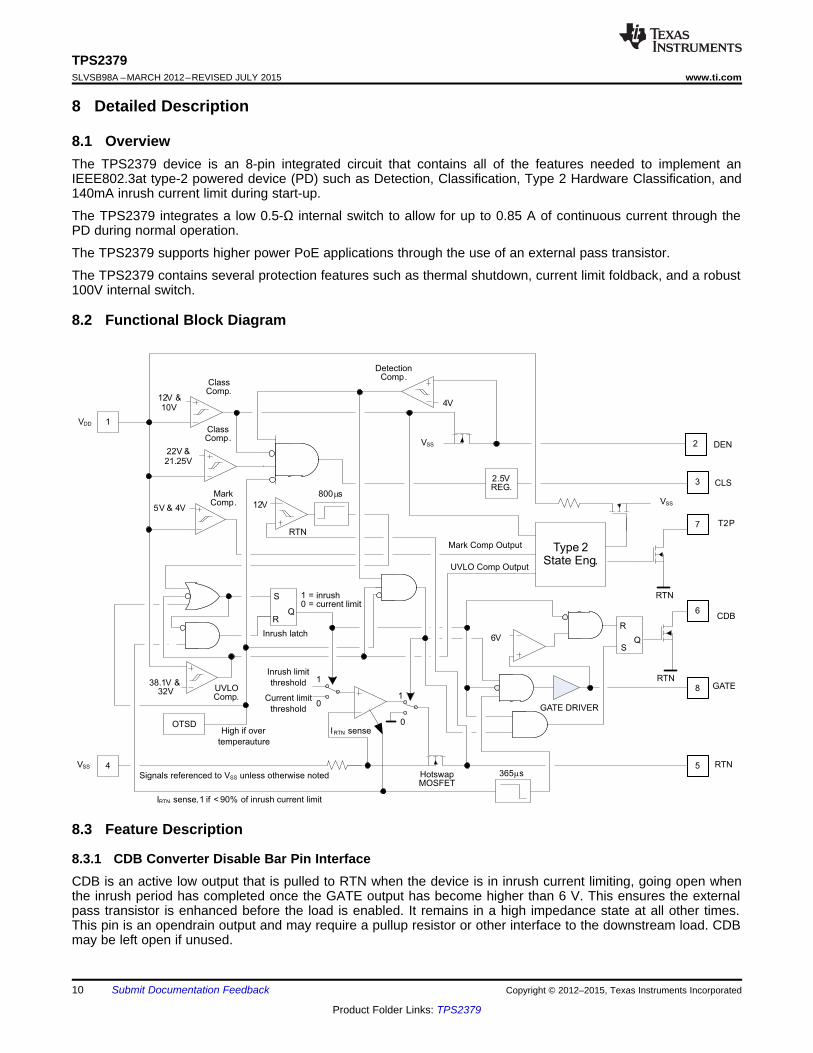
8 Detailed Description
8.1 OverviewThe TPS2379 device is an 8-pin integrated circuit that contains all of the features needed to implement anIEEE802.3at type-2 powered device (PD) such as Detection, Classification, Type 2 Hardware Classification, and140mA inrush current limit during start-up.
The TPS2379 integrates a low 0.5-Ω internal switch to allow for up to 0.85 A of continuous current through thePD during normal operation.
The TPS2379 supports higher power PoE applications through the use of an external pass transistor.
The TPS2379 contains several protection features such as thermal shutdown, current limit foldback, and a robust100V internal switch.
8.2 Functional Block Diagram
8.3 Feature Description
8.3.1 CDB Converter Disable Bar Pin InterfaceCDB is an active low output that is pulled to RTN when the device is in inrush current limiting, going open whenthe inrush period has completed once the GATE output has become higher than 6 V. This ensures the externalpass transistor is enhanced before the load is enabled. It remains in a high impedance state at all other times.This pin is an opendrain output and may require a pullup resistor or other interface to the downstream load. CDBmay be left open if unused.
10 Submit Documentation Feedback Copyright © 2012–2015, Texas Instruments Incorporated
Product Folder Links: TPS2379
TPS2379
CDB
RTN
CSS
SS
GND
UCC2897A
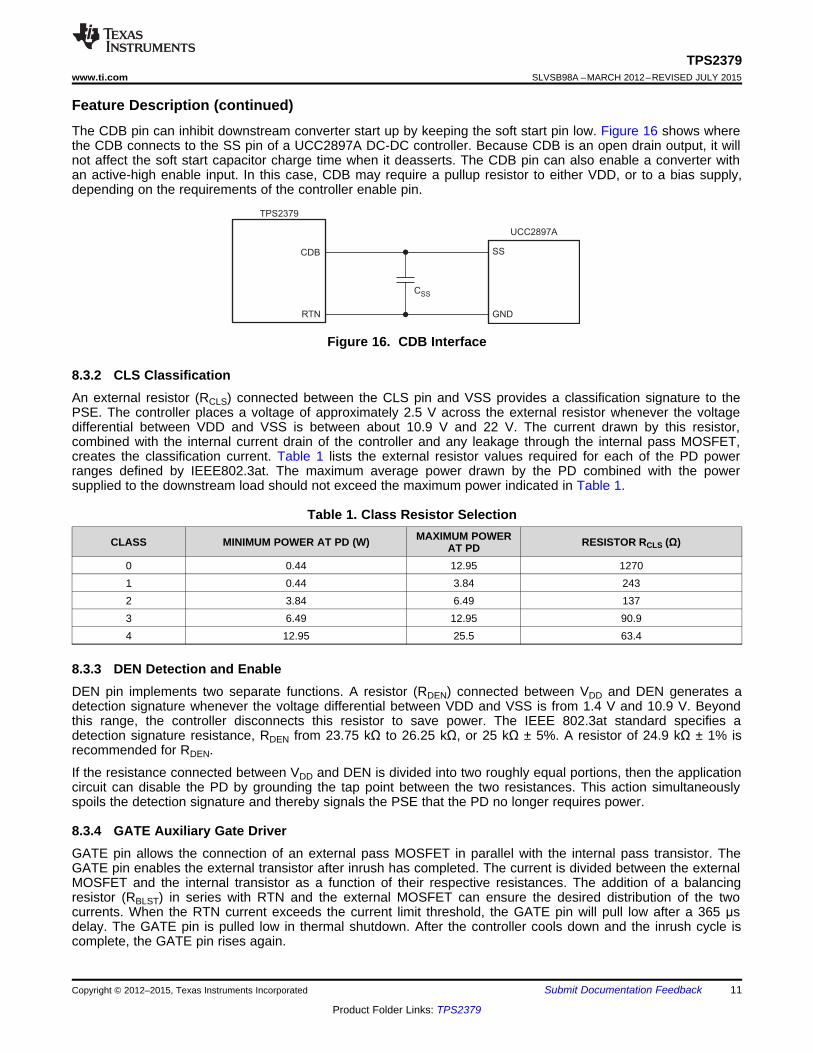
TPS2379www.ti.com SLVSB98A –MARCH 2012–REVISED JULY 2015
Feature Description (continued)The CDB pin can inhibit downstream converter start up by keeping the soft start pin low. Figure 16 shows wherethe CDB connects to the SS pin of a UCC2897A DC-DC controller. Because CDB is an open drain output, it willnot affect the soft start capacitor charge time when it deasserts. The CDB pin can also enable a converter withan active-high enable input. In this case, CDB may require a pullup resistor to either VDD, or to a bias supply,depending on the requirements of the controller enable pin.
Figure 16. CDB Interface
8.3.2 CLS ClassificationAn external resistor (RCLS) connected between the CLS pin and VSS provides a classification signature to thePSE. The controller places a voltage of approximately 2.5 V across the external resistor whenever the voltagedifferential between VDD and VSS is between about 10.9 V and 22 V. The current drawn by this resistor,combined with the internal current drain of the controller and any leakage through the internal pass MOSFET,creates the classification current. Table 1 lists the external resistor values required for each of the PD powerranges defined by IEEE802.3at. The maximum average power drawn by the PD combined with the powersupplied to the downstream load should not exceed the maximum power indicated in Table 1.
Table 1. Class Resistor SelectionMAXIMUM POWERCLASS MINIMUM POWER AT PD (W) RESISTOR RCLS (Ω)AT PD
0 0.44 12.95 12701 0.44 3.84 2432 3.84 6.49 1373 6.49 12.95 90.94 12.95 25.5 63.4
8.3.3 DEN Detection and EnableDEN pin implements two separate functions. A resistor (RDEN) connected between VDD and DEN generates adetection signature whenever the voltage differential between VDD and VSS is from 1.4 V and 10.9 V. Beyondthis range, the controller disconnects this resistor to save power. The IEEE 802.3at standard specifies adetection signature resistance, RDEN from 23.75 kΩ to 26.25 kΩ, or 25 kΩ ± 5%. A resistor of 24.9 kΩ ± 1% isrecommended for RDEN.
If the resistance connected between VDD and DEN is divided into two roughly equal portions, then the applicationcircuit can disable the PD by grounding the tap point between the two resistances. This action simultaneouslyspoils the detection signature and thereby signals the PSE that the PD no longer requires power.
8.3.4 GATE Auxiliary Gate DriverGATE pin allows the connection of an external pass MOSFET in parallel with the internal pass transistor. TheGATE pin enables the external transistor after inrush has completed. The current is divided between the externalMOSFET and the internal transistor as a function of their respective resistances. The addition of a balancingresistor (RBLST) in series with RTN and the external MOSFET can ensure the desired distribution of the twocurrents. When the RTN current exceeds the current limit threshold, the GATE pin will pull low after a 365 μsdelay. The GATE pin is pulled low in thermal shutdown. After the controller cools down and the inrush cycle iscomplete, the GATE pin rises again.
Copyright © 2012–2015, Texas Instruments Incorporated Submit Documentation Feedback 11
Product Folder Links: TPS2379

BLST Q12379 L
BLST Q1 2379
R RI I
R R R
+
= ´
+ +
TPS2379
VDD
VSS
T2P
CDB
GATE
RTN
VC
DC
/DC
Convert
er
Q2
Q1
RBLST
IL
I2379
CB
ULK
TPS2379SLVSB98A –MARCH 2012–REVISED JULY 2015 www.ti.com
A nonstandard PoE system can be designed to meet extended power requirements and retain the PoE benefits,such as protection of non-PoE devices and fault tolerance. This type of solution will not comply with IEEE802.3atand should be designed and operated as stand-alone system. The TPS2379 GATE pin controls an external passMOSFET as shown in Figure 17. When the inrush is complete, GATE sources 38 μA to enable Q1, the externalpass MOSFET. When Q1 is fully enhanced, CDB deasserts and enables the load. Delaying the deassertion ofCDB until Q1 becomes fully enhanced prevents nuisance overcurrent faults that could occur with heavy start-uploads. A resistor from GATE to VSS is not required to ensure that Q1 turns off. If a resistor from GATE to VSS isused, choose a value large enough so that the GATE sourcing current can fully enhance Q1.
Figure 17. GATE Interface
8.3.4.1 External Boost Circuit (Q1, Q2, and RBLST) ConsiderationsThe IEEE802.3at template bounds the peak PSE output current from 50 A for 10 μs and 1.75 A for 75 ms for atwo-pair system. In a nonstandard, four-pair system, these current levels may double. During an overload event,the TPS2379 device will limit current to approximately 1 A and the rest of the current will flow through Q1 andRBLST. Ignoring the ballast resistor and parasitic impedances, the current through Q1 could be as high as 99 A.
Actual system level behavior will be influenced by the circuit parasitic impedances, diode bridge impedance,contact resistances, external MOSFET resistance, and input voltage droop during the overload event. Theimpedances act to reduce the peak current as well as drop the voltage across Q1 during the overload event.Evaluate the overload performance of your system and ensure that the selected external MOSFET safeoperating area (SOA) is not violated during the output overload. The duration of the overload can be terminated ifthe input voltage droop to the TPS2379 goes below the UVLO falling threshold (typically 32 V). When UVLOoccurs, the internal MOSFET is disabled, GATE goes low and the external MOSFET is disabled. This shortenedoverload duration is beneficial when evaluating the external MOSFET SOA performance.
Additional limiting and control of the external output overload current can be achieved by using the ballastresistor, RBLST. RBLST helps balance the internal and external MOSFET load currents and implements externalcurrent limiting through Q2. The load current, IL, divides between the external Q1 and the internal pass MOSFETof the TPS2379 as shown Equation 1.
(1)
RQ1 is the ON resistance of Q1 and R2379 is the ON resistance of the TPS2379. Q2 can be used to force Q1 tolimit its current when the voltage across RBLST exceeds VBEON of Q2. For further discussion of these details andadditional considerations involving PD classification, see the application report titled Implementing a 60-W End-to-End PoE System (SLVA498).
8.3.5 Internal Pass MOSFETRTN pin provides the negative power return path for the load. When VDD exceeds the UVLO threshold, theinternal pass MOSFET pulls RTN to VSS. Inrush limiting prevents the RTN current from exceeding 140 mA untilthe bulk capacitance (CBULK in Figure 26) is fully charged. Inrush ends when the RTN current drops below about125 mA. The RTN current is subsequently limited to about 1 A. CDB pulls low to signal the downstream load thatthe bulk capacitance is fully charged. If RTN ever exceeds about 12 V for longer than 800 μs, the TPS2379returns to inrush limiting.
12 Submit Documentation Feedback Copyright © 2012–2015, Texas Instruments Incorporated
Product Folder Links: TPS2379
T2P-OUTT2P-MIN T2P
C T2P FWLEDT2P
T2P
I 0.46mAI 0.46mA, Select I 1mA
CTR 1.00
V V V 12 V 0.26 V 1.1 VR 10.6kΩ
I 1mA
= = = =
- - - -
= = =
OUT T2P OUTT2P OUT
T2P OUT
V V 5 0.4I 0.46mA
R 10000
-
-
-
- -
= = =
RT2P
VC
I T2P
I T2P
-OU
T
VOUT
RT2P-OUT
VT2P-OUT
V LowT2P
IndicatesType 2
T2P FromTPS2379
TPS2379www.ti.com SLVSB98A –MARCH 2012–REVISED JULY 2015
8.3.6 T2P Type-2 PSE IndicatorThe TPS2379 pulls T2P to RTN when type-2 hardware classification has been observed. The T2P output willreturn to a high-impedance state if the part enters thermal shutdown, the pass MOSFET enters inrush limiting, orif a type-2 PSE was not detected. The circuitry that watches for type-2 hardware classification latches its resultwhen the VDD-to-VSS voltage differential rises above the upper classification threshold. This circuit resets whenthe VDD-to-VSS voltage differential drops below the mark threshold. The T2P pin can be left unconnected ifunused.
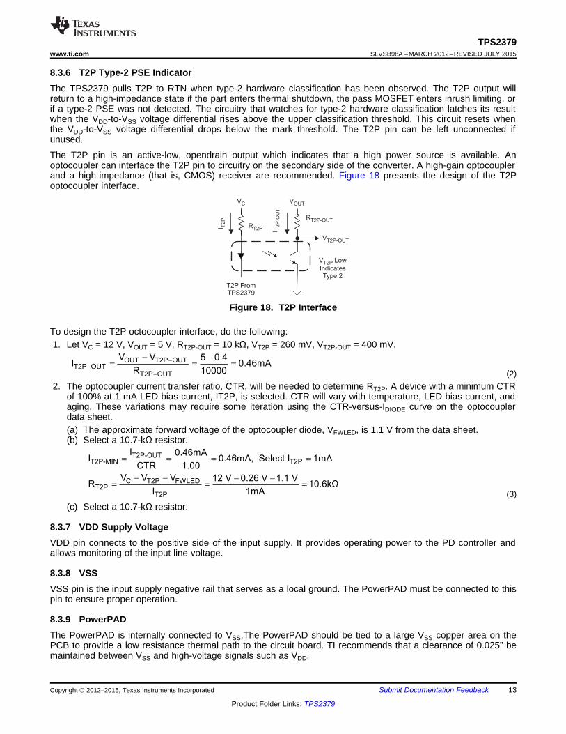
The T2P pin is an active-low, opendrain output which indicates that a high power source is available. Anoptocoupler can interface the T2P pin to circuitry on the secondary side of the converter. A high-gain optocouplerand a high-impedance (that is, CMOS) receiver are recommended. Figure 18 presents the design of the T2Poptocoupler interface.
Figure 18. T2P Interface
To design the T2P octocoupler interface, do the following:1. Let VC = 12 V, VOUT = 5 V, RT2P-OUT = 10 kΩ, VT2P = 260 mV, VT2P-OUT = 400 mV.
(2)2. The optocoupler current transfer ratio, CTR, will be needed to determine RT2P. A device with a minimum CTR
of 100% at 1 mA LED bias current, IT2P, is selected. CTR will vary with temperature, LED bias current, andaging. These variations may require some iteration using the CTR-versus-IDIODE curve on the optocouplerdata sheet.(a) The approximate forward voltage of the optocoupler diode, VFWLED, is 1.1 V from the data sheet.(b) Select a 10.7-kΩ resistor.
(3)(c) Select a 10.7-kΩ resistor.
8.3.7 VDD Supply VoltageVDD pin connects to the positive side of the input supply. It provides operating power to the PD controller andallows monitoring of the input line voltage.
8.3.8 VSSVSS pin is the input supply negative rail that serves as a local ground. The PowerPAD must be connected to thispin to ensure proper operation.
8.3.9 PowerPADThe PowerPAD is internally connected to VSS.The PowerPAD should be tied to a large VSS copper area on thePCB to provide a low resistance thermal path to the circuit board. TI recommends that a clearance of 0.025” bemaintained between VSS and high-voltage signals such as VDD.
Copyright © 2012–2015, Texas Instruments Incorporated Submit Documentation Feedback 13
Product Folder Links: TPS2379
574237
3020.514.510.12.7
De
tec
tio
nL
ow
er
Lim
it
De
tec
tio
nU
pp
er
Lim
it
Cla
ss
ific
ati
on
Lo
we
rL
imit
Cla
ss
ific
ati
on
Up
pe
rL
imit
Mu
st
Tu
rnO
ffb
y-
Vo
lta
ge
Fa
llin
g
Lo
we
rL
imit
-O
pe
rati
ng
Ra
ng
e
Mu
st
Tu
rnO
nb
y-
Vo
lta
ge
Ris
ing
Ma
xim
um
Inp
ut
Vo
lta
ge
Detect ClassifyShut-down
PI Voltage (V)0
Lo
we
rL
imit
-1
3W
Op
.
Mark
Cla
ss
-Ma
rkT
ran
sit
ion
25
0m
sT
ran
sie
nt
6.9
Normal Operation
IEE
E8
02
.3a
t
Normal Operation
T2
Re
se
tR
an
ge
42.5
IEE
E 8
02
-20
08
TPS2379SLVSB98A –MARCH 2012–REVISED JULY 2015 www.ti.com
8.4 Device Functional Modes
8.4.1 PoE OverviewThe following text is intended as an aid in understanding the operation of the TPS2379 but not as a substitute forthe IEEE 802.3at standard. The IEEE 802.3at standard is an update to IEEE 802.3-2008 clause 33 (PoE),adding high-power options and enhanced classification. Generally speaking, a device compliant to IEEE 802.3-2008 is referred to as a type 1 device, and devices with high power and enhanced classification will be referredto as type 2 devices. Standards change and should always be referenced when making design decisions.
The IEEE 802.3at standard defines a method of safely powering a PD (powered device) over a cable by powersourcing equipment (PSE), and then removing power if a PD is disconnected. The process proceeds through anidle state and three operational states of detection, classification, and operation. The PSE leaves the cableunpowered (idle state) while it periodically looks to see if something has been plugged in; this is referred to asdetection. The low power levels used during detection are unlikely to damage devices not designed for PoE. If avalid PD signature is present, the PSE may inquire how much power the PD requires; this is referred to asclassification. The PSE may then power the PD if it has adequate capacity.
Type 2 PSEs are required to do type 1 hardware classification plus a (new) data-layer classification, or anenhanced type 2 hardware classification. Type 1 PSEs are not required to do hardware or data link layer (DLL)classification. A type 2 PD must do type 2 hardware classification as well as DLL classification. The PD mayreturn the default, 13W current-encoded class, or one of four other choices. DLL classification occurs afterpower-on and the Ethernet data link has been established.
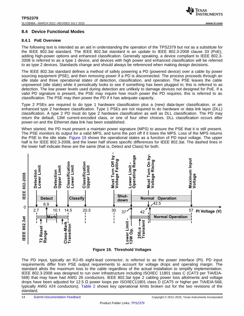
When started, the PD must present a maintain power signature (MPS) to assure the PSE that it is still present.The PSE monitors its output for a valid MPS, and turns the port off if it loses the MPS. Loss of the MPS returnsthe PSE to the idle state. Figure 19 shows the operational states as a function of PD input voltage. The upperhalf is for IEEE 802.3-2008, and the lower half shows specific differences for IEEE 802.3at. The dashed lines inthe lower half indicate these are the same (that is, Detect and Class) for both.
Figure 19. Threshold Voltages
The PD input, typically an RJ-45 eight-lead connector, is referred to as the power interface (PI). PD inputrequirements differ from PSE output requirements to account for voltage drops and operating margin. Thestandard allots the maximum loss to the cable regardless of the actual installation to simplify implementation.IEEE 802.3-2008 was designed to run over infrastructure including ISO/IEC 11801 class C (CAT3 per TIA/EIA-568) that may have had AWG 26 conductors. IEEE 802.3at type 2 cabling power loss allotments and voltagedrops have been adjusted for 12.5 Ω power loops per ISO/IEC11801 class D (CAT5 or higher per TIA/EIA-568,typically AWG #24 conductors). Table 2 shows key operational limits broken out for the two revisions of thestandard.14 Submit Documentation Feedback Copyright © 2012–2015, Texas Instruments Incorporated
Product Folder Links: TPS2379
VUVLO_R
Detection
Classification
PD Powered
Idle
VCL_ON
VCL_H
VCU_OFF
VCU_H
Note: Variable names refer to Electrical Characteristic Table parameters
VDD-VSS
VUVLO_H
Mark
VMSR
Fu
nctio
na
l
Sta
te
Typ
e2
Type 1
TPS2379www.ti.com SLVSB98A –MARCH 2012–REVISED JULY 2015
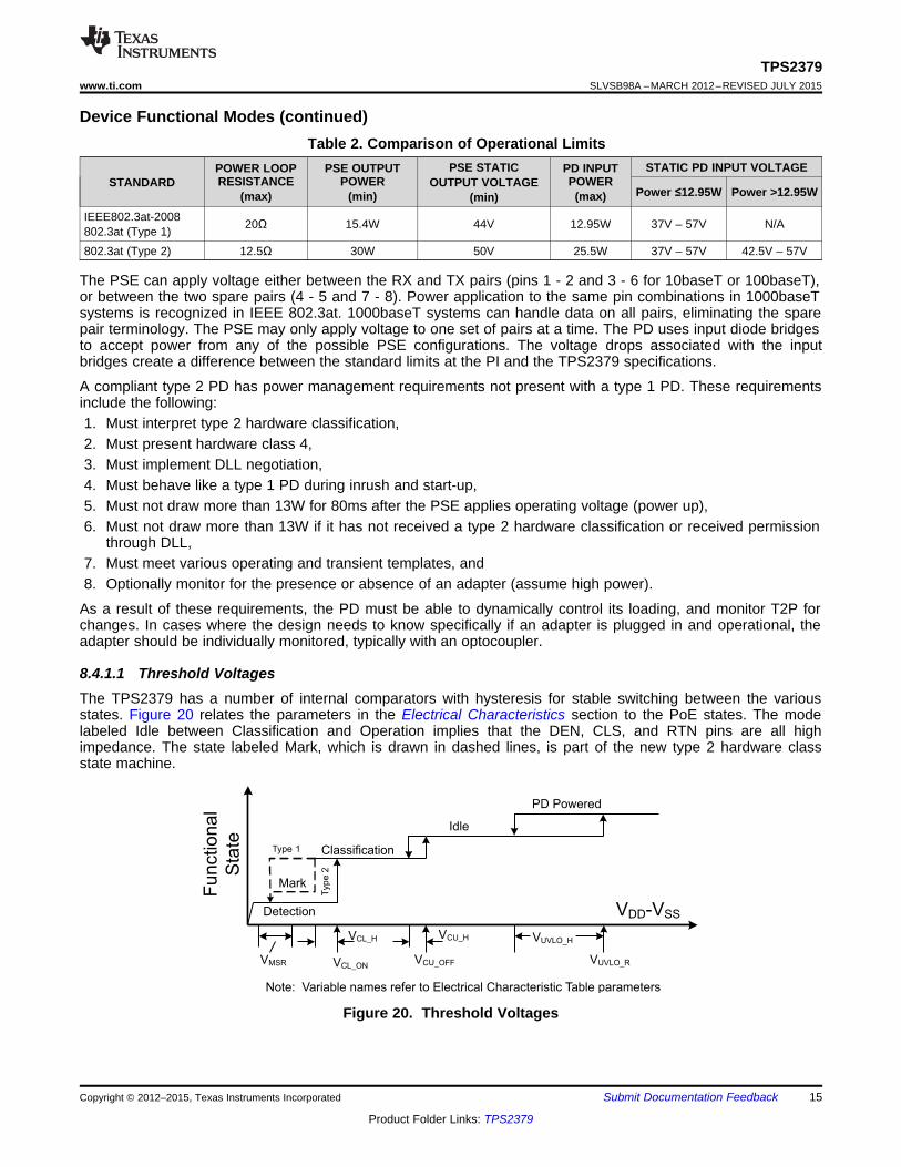
Device Functional Modes (continued)Table 2. Comparison of Operational Limits
PSE STATIC STATIC PD INPUT VOLTAGEPOWER LOOP PSE OUTPUT PD INPUTRESISTANCE POWER POWERSTANDARD OUTPUT VOLTAGE
Power ≤12.95W Power >12.95W(max) (min) (max)(min)IEEE802.3at-2008 20Ω 15.4W 44V 12.95W 37V – 57V N/A802.3at (Type 1)802.3at (Type 2) 12.5Ω 30W 50V 25.5W 37V – 57V 42.5V – 57V
The PSE can apply voltage either between the RX and TX pairs (pins 1 - 2 and 3 - 6 for 10baseT or 100baseT),or between the two spare pairs (4 - 5 and 7 - 8). Power application to the same pin combinations in 1000baseTsystems is recognized in IEEE 802.3at. 1000baseT systems can handle data on all pairs, eliminating the sparepair terminology. The PSE may only apply voltage to one set of pairs at a time. The PD uses input diode bridgesto accept power from any of the possible PSE configurations. The voltage drops associated with the inputbridges create a difference between the standard limits at the PI and the TPS2379 specifications.
A compliant type 2 PD has power management requirements not present with a type 1 PD. These requirementsinclude the following:1. Must interpret type 2 hardware classification,2. Must present hardware class 4,3. Must implement DLL negotiation,4. Must behave like a type 1 PD during inrush and start-up,5. Must not draw more than 13W for 80ms after the PSE applies operating voltage (power up),6. Must not draw more than 13W if it has not received a type 2 hardware classification or received permission
through DLL,7. Must meet various operating and transient templates, and8. Optionally monitor for the presence or absence of an adapter (assume high power).
As a result of these requirements, the PD must be able to dynamically control its loading, and monitor T2P forchanges. In cases where the design needs to know specifically if an adapter is plugged in and operational, theadapter should be individually monitored, typically with an optocoupler.
8.4.1.1 Threshold VoltagesThe TPS2379 has a number of internal comparators with hysteresis for stable switching between the variousstates. Figure 20 relates the parameters in the Electrical Characteristics section to the PoE states. The modelabeled Idle between Classification and Operation implies that the DEN, CLS, and RTN pins are all highimpedance. The state labeled Mark, which is drawn in dashed lines, is part of the new type 2 hardware classstate machine.
Figure 20. Threshold Voltages
Copyright © 2012–2015, Texas Instruments Incorporated Submit Documentation Feedback 15
Product Folder Links: TPS2379

Time: 50ms/div
IPI
Inrush
Load enabled using
CDB plus delay
Detect
Class Mark
VVDD-VSS
VRTN-VSS
Vo
ltag
e:
10 V
/div
Cu
rren
t: 1
00 m
A/d
iv
TPS2379SLVSB98A –MARCH 2012–REVISED JULY 2015 www.ti.com
8.4.1.2 PoE Start-Up SequenceThe waveforms of Figure 21 demonstrate detection, classification, and start-up from a PSE with type 2 hardwareclassification. The key waveforms shown are V(VDD-VSS), V(RTN-VSS), and IPI. IEEE 802.3at requires aminimum of two detection levels, two class and mark cycles, and start-up from the second mark event. VRTN toVSS falls as the TPS2379 charges CBULK following application of full voltage. In Figure 21, deassertion of the CDBsignal is delayed and used to enable load current as seen in the IPI waveform.
Figure 21. Start-up
8.4.1.3 DetectionThe TPS2379 pulls DEN to VSS whenever V(VDD-VSS) is below the lower classification threshold. When the inputvoltage rises above VCL-ON, the DEN pin goes to an opendrain condition to conserve power. While in detection,RTN is high impedance, and almost all the internal circuits are disabled. An RDEN of 24.9 kΩ (±1%), presents thecorrect signature. It may be a small, low-power resistor because it only sees a stress of about 5 mW. A valid PDdetection signature is an incremental resistance ( ΔV/ΔI ) between 23.75 kΩ and 26.25 kΩ at the PI.
The detection resistance seen by the PSE at the PI is the result of the input bridge resistance in series with theparallel combination of RDEN and internal VDD loading. The input diode bridge’s incremental resistance may behundreds of ohms at the very low currents drawn when 2.7 V is applied to the PI. The input bridge resistance ispartially compensated by the TPS2379's effective resistance during detection.
The type 2 hardware classification protocol of IEEE 802.3at specifies that a type 2 PSE drops its output voltageinto the detection range during the classification sequence. The PD is required to have an incorrect detectionsignature in this condition, which is referred to as a mark event (see Figure 21). After the first mark event, theTPS2379 will present a signature less than 12 kΩ until it has experienced a V(VDD-VSS) voltage below the markreset threshold (VMSR). This is explained more fully under Hardware Classification.
8.4.1.4 Hardware ClassificationHardware classification allows a PSE to determine a PD’s power requirements before powering, and helps withpower management once power is applied. Type 2 hardware classification permits high power PSEs and PDs todetermine whether the connected device can support high-power operation. A type 2 PD presents class 4 inhardware to indicate that it is a high-power device. A type 1 PSE will treat a class 4 device like a class 0 device,allotting 13 W if it chooses to power the PD. A PD that receives a 2-event class understands that it is poweredfrom a high-power PSE and it may draw up to 25.5 W immediately after the 80 ms start-up period completes. Atype 2 PD that does not receive a 2-event hardware classification may choose to not start, or must start in a 13W condition and request more power through the DLL after start-up. The standard requires a type 2 PD toindicate that it is underpowered if this occurs. Start-up of a high-power PD under 13 W implicitly requires someform of powering down sections of the application circuits.
16 Submit Documentation Feedback Copyright © 2012–2015, Texas Instruments Incorporated
Product Folder Links: TPS2379
Detect Class
Mark Class
Mark ClassBetween
Ranges
Between
Ranges
Operating
T2Popen-drain
Operating
T2P low
Between
Ranges
UVLO
Rising
UVLO
Falling
UVLO
Rising
UVLO
Falling
TYPE 2 PSE
Hardware Class
Class
TYPE 1 PSE
Hardware Class
Between
Ranges
PoE Startup Sequence
Mark
Reset
Idle
TPS2379www.ti.com SLVSB98A –MARCH 2012–REVISED JULY 2015
The maximum power entries in Table 1 determine the class the PD must advertise. The PSE may disconnect aPD if it draws more than its stated Class power, which may be the hardware class or a lower DLL-derived powerlevel. The standard permits the PD to draw limited current peaks that increase the instantaneous power abovethe Table 1 limit, however the average power requirement always applies.
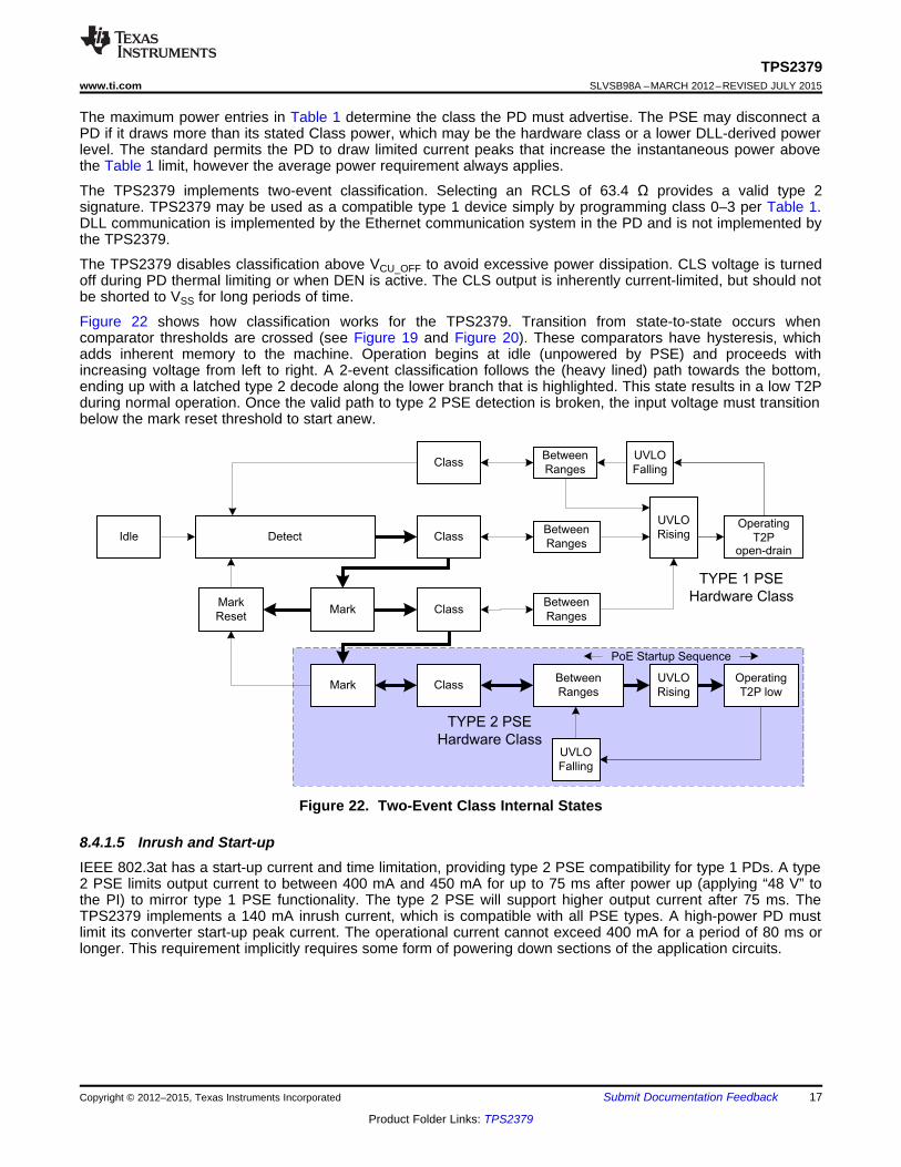
The TPS2379 implements two-event classification. Selecting an RCLS of 63.4 Ω provides a valid type 2signature. TPS2379 may be used as a compatible type 1 device simply by programming class 0–3 per Table 1.DLL communication is implemented by the Ethernet communication system in the PD and is not implemented bythe TPS2379.
The TPS2379 disables classification above VCU_OFF to avoid excessive power dissipation. CLS voltage is turnedoff during PD thermal limiting or when DEN is active. The CLS output is inherently current-limited, but should notbe shorted to VSS for long periods of time.
Figure 22 shows how classification works for the TPS2379. Transition from state-to-state occurs whencomparator thresholds are crossed (see Figure 19 and Figure 20). These comparators have hysteresis, whichadds inherent memory to the machine. Operation begins at idle (unpowered by PSE) and proceeds withincreasing voltage from left to right. A 2-event classification follows the (heavy lined) path towards the bottom,ending up with a latched type 2 decode along the lower branch that is highlighted. This state results in a low T2Pduring normal operation. Once the valid path to type 2 PSE detection is broken, the input voltage must transitionbelow the mark reset threshold to start anew.
Figure 22. Two-Event Class Internal States
8.4.1.5 Inrush and Start-upIEEE 802.3at has a start-up current and time limitation, providing type 2 PSE compatibility for type 1 PDs. A type2 PSE limits output current to between 400 mA and 450 mA for up to 75 ms after power up (applying “48 V” tothe PI) to mirror type 1 PSE functionality. The type 2 PSE will support higher output current after 75 ms. TheTPS2379 implements a 140 mA inrush current, which is compatible with all PSE types. A high-power PD mustlimit its converter start-up peak current. The operational current cannot exceed 400 mA for a period of 80 ms orlonger. This requirement implicitly requires some form of powering down sections of the application circuits.
Copyright © 2012–2015, Texas Instruments Incorporated Submit Documentation Feedback 17
Product Folder Links: TPS2379
Time: 5ms/div
10V/div
100mA/div
IPI
Inrush
Load enabled usingCDB plus delay
VVDD-RTN
VCDB-RTN
VT2P-RTN50V/div
50V/div
PI powered
Type 1 PSE
Type 2 PSE
V(GATE-VSS)
10V/div
TPS2379SLVSB98A –MARCH 2012–REVISED JULY 2015 www.ti.com
8.4.1.6 Maintain Power SignatureThe MPS is an electrical signature presented by the PD to assure the PSE that it is still present after operatingvoltage is applied. A valid MPS consists of a minimum DC current of 10 mA (or a 10 mA pulsed current for atleast 75 ms every 325 ms) and an AC impedance lower than 26.3 kΩ in parallel with 0.05 μF. The ACimpedance is usually accomplished by the minimum operating CBULK requirement of 5 μF. When DEN is used toforce the hotswap switch off, the DC MPS will not be met. A PSE that monitors the DC MPS will remove powerfrom the PD when this occurs. A PSE that monitors only the ac MPS may remove power from the PD.
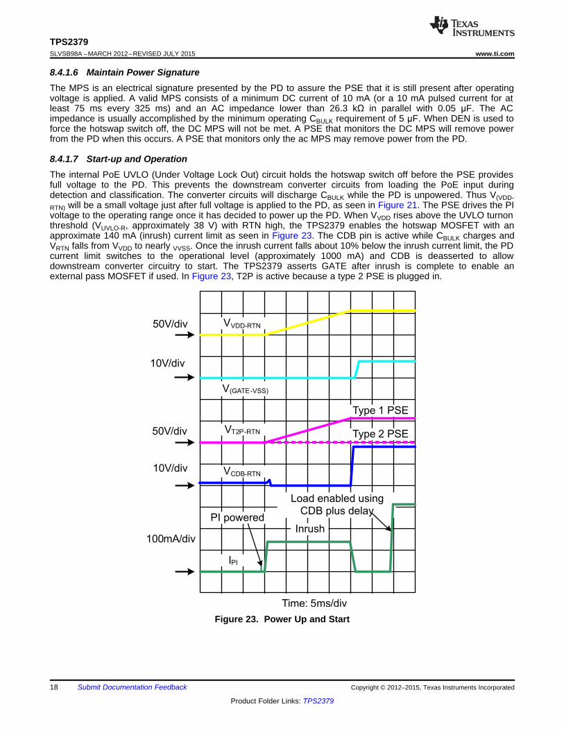
8.4.1.7 Start-up and OperationThe internal PoE UVLO (Under Voltage Lock Out) circuit holds the hotswap switch off before the PSE providesfull voltage to the PD. This prevents the downstream converter circuits from loading the PoE input duringdetection and classification. The converter circuits will discharge CBULK while the PD is unpowered. Thus V(VDD-RTN) will be a small voltage just after full voltage is applied to the PD, as seen in Figure 21. The PSE drives the PIvoltage to the operating range once it has decided to power up the PD. When VVDD rises above the UVLO turnonthreshold (VUVLO-R, approximately 38 V) with RTN high, the TPS2379 enables the hotswap MOSFET with anapproximate 140 mA (inrush) current limit as seen in Figure 23. The CDB pin is active while CBULK charges andVRTN falls from VVDD to nearly VVSS. Once the inrush current falls about 10% below the inrush current limit, the PDcurrent limit switches to the operational level (approximately 1000 mA) and CDB is deasserted to allowdownstream converter circuitry to start. The TPS2379 asserts GATE after inrush is complete to enable anexternal pass MOSFET if used. In Figure 23, T2P is active because a type 2 PSE is plugged in.
Figure 23. Power Up and Start
18 Submit Documentation Feedback Copyright © 2012–2015, Texas Instruments Incorporated
Product Folder Links: TPS2379
Time: 200us/div
20V/div
500mA/divIPI
Inrush
VRTN-VSS > 12V
VRTN-VSS
VCDB-VSS
20V/div
5V/div
VGATE-VSS
TPS2379www.ti.com SLVSB98A –MARCH 2012–REVISED JULY 2015
8.4.1.8 PD Hotswap OperationIEEE 802.3at has taken a new approach to PSE output limiting. A type 2 PSE must meet an output currentversus time template with specified minimum and maximum sourcing boundaries. The peak output current maybe as high as 50 A for 10 μs or 1.75 A for 75 ms. This makes robust protection of the PD device even moreimportant than it was in IEEE 802.3-2008.
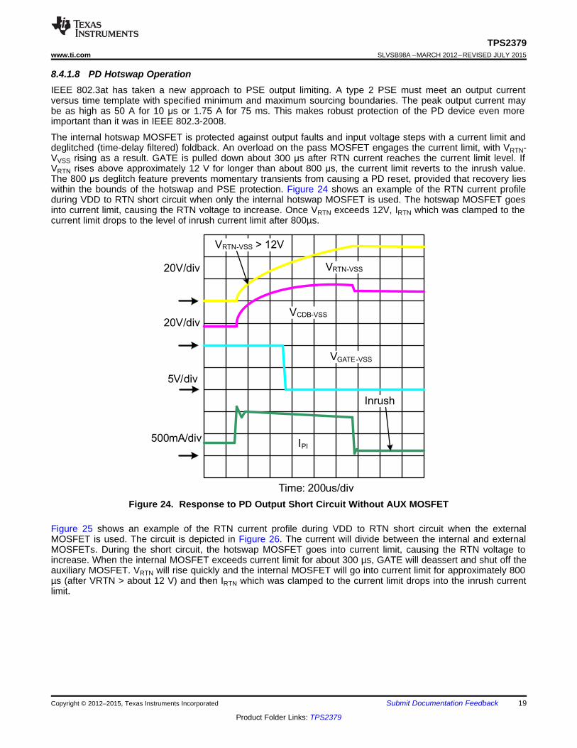
The internal hotswap MOSFET is protected against output faults and input voltage steps with a current limit anddeglitched (time-delay filtered) foldback. An overload on the pass MOSFET engages the current limit, with VRTN-VVSS rising as a result. GATE is pulled down about 300 μs after RTN current reaches the current limit level. IfVRTN rises above approximately 12 V for longer than about 800 μs, the current limit reverts to the inrush value.The 800 μs deglitch feature prevents momentary transients from causing a PD reset, provided that recovery lieswithin the bounds of the hotswap and PSE protection. Figure 24 shows an example of the RTN current profileduring VDD to RTN short circuit when only the internal hotswap MOSFET is used. The hotswap MOSFET goesinto current limit, causing the RTN voltage to increase. Once VRTN exceeds 12V, IRTN which was clamped to thecurrent limit drops to the level of inrush current limit after 800µs.
Figure 24. Response to PD Output Short Circuit Without AUX MOSFET
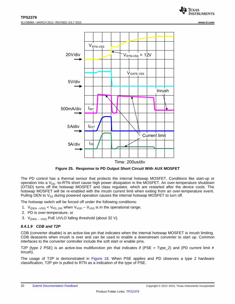
Figure 25 shows an example of the RTN current profile during VDD to RTN short circuit when the externalMOSFET is used. The circuit is depicted in Figure 26. The current will divide between the internal and externalMOSFETs. During the short circuit, the hotswap MOSFET goes into current limit, causing the RTN voltage toincrease. When the internal MOSFET exceeds current limit for about 300 µs, GATE will deassert and shut off theauxiliary MOSFET. VRTN will rise quickly and the internal MOSFET will go into current limit for approximately 800µs (after VRTN > about 12 V) and then IRTN which was clamped to the current limit drops into the inrush currentlimit.
Copyright © 2012–2015, Texas Instruments Incorporated Submit Documentation Feedback 19
Product Folder Links: TPS2379
Time: 200us/div
20V/div
500mA/div
IPI
Inrush
VRTN-VSS > 12V
VRTN-VSS
5V/div
VGATE-VSS
IINT
IEXT
5A/div
5A/div
Current limit
TPS2379SLVSB98A –MARCH 2012–REVISED JULY 2015 www.ti.com
Figure 25. Response to PD Output Short Circuit With AUX MOSFET
The PD control has a thermal sensor that protects the internal hotswap MOSFET. Conditions like start-up oroperation into a VDD -to-RTN short cause high power dissipation in the MOSFET. An over-temperature shutdown(OTSD) turns off the hotswap MOSFET and class regulator, which are restarted after the device cools. Thehotswap MOSFET will be re-enabled with the inrush current limit when exiting from an over-temperature event.Pulling DEN to VSS during powered operation causes the internal hotswap MOSFET to turn off.
The hotswap switch will be forced off under the following conditions:1. V(DEN –VSS) < VPD_DIS when VVDD – VVSS is in the operational range,2. PD is over-temperature, or3. V(DEN – VSS) PoE UVLO falling threshold (about 32 V).
8.4.1.9 CDB and T2PCDB (converter disable) is an active-low pin that indicates when the internal hotswap MOSFET is inrush limiting.CDB deasserts when inrush is over and can be used to enable a downstream converter to start up. Commoninterfaces to the converter controller include the soft start or enable pins.
T2P (type 2 PSE) is an active-low multifunction pin that indicates if (PSE = Type_2) and (PD current limit ≠Inrush).
The usage of T2P is demonstrated in Figure 18. When PSE applies and PD observes a type 2 hardwareclassification, T2P pin is pulled to RTN as a indication of the type of PSE.
20 Submit Documentation Feedback Copyright © 2012–2015, Texas Instruments Incorporated
Product Folder Links: TPS2379
TPS2379www.ti.com SLVSB98A –MARCH 2012–REVISED JULY 2015
8.4.1.10 Auxiliary Pass MOSFET ControlThe TPS2379 can be used in non-standard applications requiring power significantly above the IEEE802.3at,type 2 levels. This implementation can be achieved by utilizing all four Ethernet wire pairs and boosting theTPS2379 hotswap MOSFET operating current limit. Boosting the TPS2379 operating current limit is achieved byadding an external pass MOSFET to share the total load current with the internal hotswap MOSFET. Theexternal pass MOSFET is enabled by the GATE pin after the internal hotswap MOSFET inrush is complete. TheGATE pin will deassert if the TPS2379 internal current limit is exceeded in excess of 300 µs.
A comprehensive high power POE design example is discussed in application report Implementing a 60-W, End-to-End PoE System (SLVA498).
8.4.1.11 Using DEN to Disable PoEThe DEN pin may be used to turn the PoE hotswap switch off by pulling it to VSS while in the operational state,or to prevent detection when in the idle state. A low voltage on DEN forces the hotswap MOSFET off duringnormal operation.
Copyright © 2012–2015, Texas Instruments Incorporated Submit Documentation Feedback 21
Product Folder Links: TPS2379
2379BLST 2379 Q1
L 2379
I 1AR R R 0.42 0.064 0.27
I I 2.26A 1A= - = W - W = W
- -
RTN
VC
VSS
CLS
DEN
CDB
T2P
GATE
TPS2379
SS
Q1
C1
D1
RDEN
RCLS
RBLST
VDDRT2P
CBULK
DC
/DC
Co
nv
ert
er
Fro
m E
the
rne
tTra
ns
form
ers
Fro
m S
pa
reP
air
s o
rTra
ns
form
ers
TPS2379SLVSB98A –MARCH 2012–REVISED JULY 2015 www.ti.com
9 Application and Implementation
NOTEInformation in the following applications sections is not part of the TI componentspecification, and TI does not warrant its accuracy or completeness. TI’s customers areresponsible for determining suitability of components for their purposes. Customers shouldvalidate and test their design implementation to confirm system functionality.
9.1 Application InformationThe TPS2379 has the flexibility to be implemented in IEEE802.3at PDs, Universal Power Over Ethernet (UPOE)PDs, or high power non-standard PDs. Therefore, it can be used in a wide range applications such as video andVoIP telephones, multiband access points, security cameras, and pico-base stations.
9.2 Typical Application
Figure 26. Typical Application Circuit
9.2.1 Design Requirements
Table 3. TPS2379EVM Electrical and Performance SpecificationsPARAMETER TEST CONDITIONS MIN TYP MAX UNIT
POWER INTERFACEInput voltage Applied to the power pins of connectors J1 or J3 0 57 VOperating voltage After start-up 30 57 V
Rising input voltage at device terminals 40Input UVLO V
Falling input voltage 30.5Detection voltage At device terminals 1.4 10.1 VClassification voltage At device terminals 11.9 23 VDetection signature 24.9 kΩClassification current Class 4 38 42 mAInrush current limit 100 180 mAOperating current limit Internal plus external 2260 mA
9.2.2 Detailed Design Procedures
Given in Equation 5, RBLST can be calulated using Equation 4
(4)
FMMT493TC can be used for Q2.
22 Submit Documentation Feedback Copyright © 2012–2015, Texas Instruments Incorporated
Product Folder Links: TPS2379
BLST Q12379 L
BLST Q1 2379
R RI I
R R R
+
= ´
+ +
TPS2379www.ti.com SLVSB98A –MARCH 2012–REVISED JULY 2015
9.2.2.1 Input Bridges and Schottky DiodesUsing Schottky diodes instead of PN junction diodes for the PoE input bridges will reduce the power dissipationin these devices by about 30%. There are, however, some things to consider when using them.
The IEEE standard specifies a maximum backfeed voltage of 2.8 V. A 100 kΩ resistor is placed between theunpowered pairs and the voltage is measured across the resistor. Schottky diodes often have a higher reverseleakage current than PN diodes, making this a harder requirement to meet. To compensate, use conservativedesign for diode operating temperature, select lower-leakage devices where possible, and match leakage andtemperatures by using packaged bridges.
Schottky diode leakage currents and lower dynamic resistances can impact the detection signature. Settingreasonable expectations for the temperature range over which the detection signature is accurate is the simplestsolution. Increasing RDEN slightly may also help meet the requirement.
Schottky diodes have proven less robust to the stresses of ESD transients than PN junction diodes. Afterexposure to ESD, Schottky diodes may become shorted or leak. Take care to provide adequate protection in linewith the exposure levels. This protection may be as simple as ferrite beads and capacitors.
As a general recommendation, use 1 A or 2 A, 100 V rated discrete or bridge diodes for the input rectifiers.
9.2.2.2 Protection, D1A TVS, D1, across the rectified PoE voltage per Figure 26 must be used. A SMAJ58A, or equivalent, isrecommended for general indoor applications. Adequate capacitive filtering or a TVS must limit input transientvoltage to within the absolute maximum ratings. Outdoor transient levels or special applications require additionalprotection.
9.2.2.3 Capacitor, C1
The IEEE 802.3at standard specifies an input bypass capacitor (from VDD to VSS) of 0.05 μF to 0.12 μF.Typically a 0.1 μF, 100 V, 10% ceramic capacitor is used.
9.2.2.4 Detection Resistor, RDEN
The IEEE 802.3at standard specifies a detection signature resistance, RDEN between 23.75 kΩ and 26.25 kΩ, or25 kΩ ± 5%. A resistor of 24.9 kΩ ± 1% is recommended for RDEN.
9.2.2.5 Classification Resistor, RCLSSelect RCLS according to Table 1. For Class 4, choose RCLS = 63.4 Ω.
9.2.2.6 External Boost CircuitFor a PD application requiring current limit of 2.26 A at the PD input (approximately 96 W) and using Q1 FETBUK7275-100A
(5)
Copyright © 2012–2015, Texas Instruments Incorporated Submit Documentation Feedback 23
Product Folder Links: TPS2379
Time: 5ms/div
10V/div
100mA/div
IPI
Inrush
Load enabled usingCDB plus delay
VVDD-RTN
VCDB-RTN
VT2P-RTN50V/div
50V/div
PI powered
Type 1 PSE
Type 2 PSE
V(GATE-VSS)
10V/div
Time: 50ms/div
IPI
Inrush
Load enabled using
CDB plus delay
Detect
Class Mark
VVDD-VSS
VRTN-VSS
Vo
lta
ge
: 1
0 V
/div
Cu
rre
nt:
10
0 m
A/d
iv
TPS2379SLVSB98A –MARCH 2012–REVISED JULY 2015 www.ti.com
9.2.3 Application Curves
Figure 28. Start-upFigure 27. Power Up and Start
24 Submit Documentation Feedback Copyright © 2012–2015, Texas Instruments Incorporated
Product Folder Links: TPS2379
TPS2379www.ti.com SLVSB98A –MARCH 2012–REVISED JULY 2015
10 Power Supply RecommendationsThe TPS2379 will typically be followed by a power supply such as an isolated flyback or active clamp forwardconverter or a non-isolated buck converter. The input voltage of the converter should be capable of operatingwithin the IEEE802.3at recommended input voltage as shown in Table 2.
11 Layout
11.1 Layout GuidelinesThe layout of the PoE front end should follow power and EMI/ESD best practice guidelines. A basic set ofrecommendations include:• Parts placement must be driven by power flow in a point-to-point manner; RJ-45, Ethernet transformer, diode
bridges, TVS and 0.1-μF capacitor, and TPS2379.• All leads should be as short as possible with wide power traces and paired signal and return.• There should not be any crossovers of signals from one part of the flow to another.• Spacing consistent with safety standards like IEC60950 must be observed between the 48-V input voltage
rails and between the input and an isolated converter output.• The TPS2379 should be located over split, local ground planes referenced to VSS for the PoE input and to
RTN for the switched output.• Large copper fills and traces should be used on SMT power-dissipating devices, and wide traces or overlay
copper fills should be used in the power path.
11.1.1 EMI Containment• Use compact loops for dv/dt and di/dt circuit paths (power loops and gate drives)• Use minimal, yet thermally adequate, copper areas for heat sinking of components tied to switching nodes
(minimize exposed radiating surface).• Use copper ground planes (possible stitching) and top layer copper floods (surround circuitry with ground
floods)• Use 4 layer PCB if economically feasible (for better grounding)• Minimize the amount of copper area associated with input traces (to minimize radiated pickup)• Use Bob Smith terminations, Bob Smith EFT capacitor, and Bob Smith plane• Use Bob Smith plane as ground shield on input side of PCB (creating a phantom or literal earth ground)• Use of ferrite beads on input (allow for possible use of beads or 0 ohm resistors)• Maintain physical separation between input-related circuitry and power circuitry (use ferrite beads as
boundary line)• Possible use of common-mode inductors• Possible use of integrated RJ-45 jacks (shielded with internal transformer and Bob Smith terminations)• End-product enclosure considerations (shielding)
Copyright © 2012–2015, Texas Instruments Incorporated Submit Documentation Feedback 25
Product Folder Links: TPS2379
TPS2379SLVSB98A –MARCH 2012–REVISED JULY 2015 www.ti.com
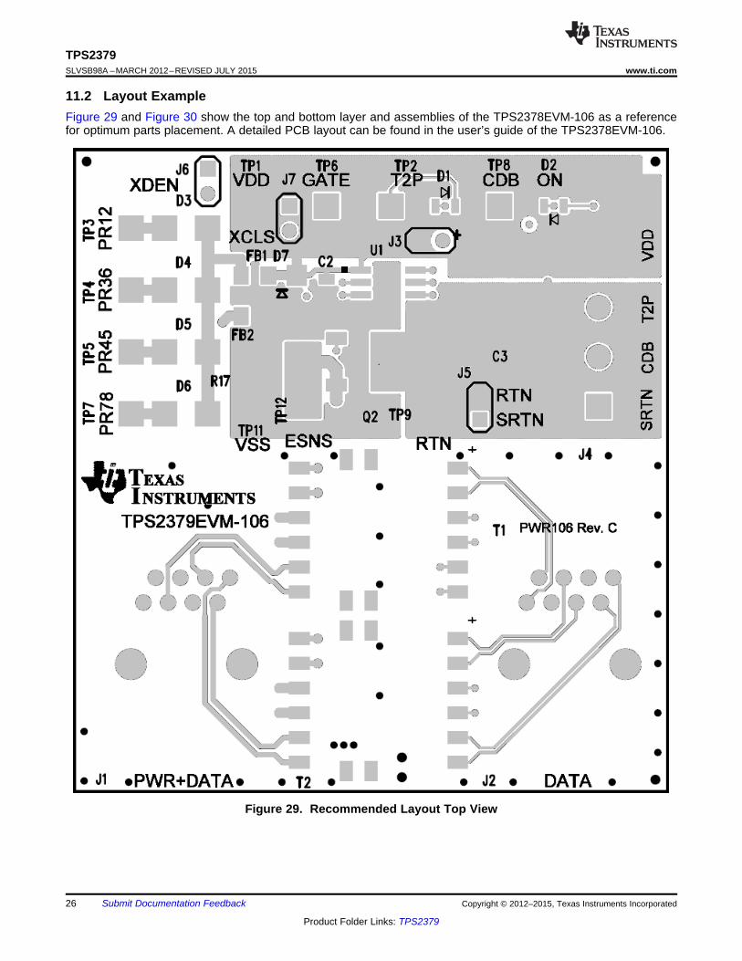
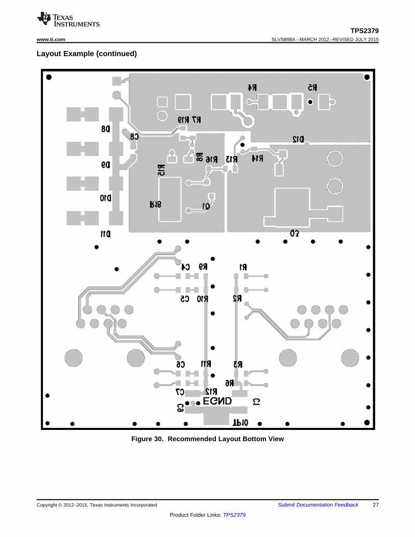
11.2 Layout ExampleFigure 29 and Figure 30 show the top and bottom layer and assemblies of the TPS2378EVM-106 as a referencefor optimum parts placement. A detailed PCB layout can be found in the user’s guide of the TPS2378EVM-106.
Figure 29. Recommended Layout Top View
26 Submit Documentation Feedback Copyright © 2012–2015, Texas Instruments Incorporated
Product Folder Links: TPS2379
TPS2379www.ti.com SLVSB98A –MARCH 2012–REVISED JULY 2015
Layout Example (continued)
Figure 30. Recommended Layout Bottom View
Copyright © 2012–2015, Texas Instruments Incorporated Submit Documentation Feedback 27
Product Folder Links: TPS2379
TPS2379SLVSB98A –MARCH 2012–REVISED JULY 2015 www.ti.com
11.3 Thermal Considerations and OTSDSources of nearby local PCB heating should be considered during the thermal design. Typical calculationsassume that the TPS2379 device is the only heat source contributing to the PCB temperature rise. It is possiblefor a normally operating TPS2379 device to experience an OTSD event if it is excessively heated by a nearbydevice.
11.4 ESDESD requirements for a unit that incorporates the TPS2379 device have a much broader scope and operationalimplications than are used in TI’s testing. Unit-level requirements should not be confused with reference designtesting that only validates the ruggedness of the TPS2379 device.
28 Submit Documentation Feedback Copyright © 2012–2015, Texas Instruments Incorporated
Product Folder Links: TPS2379
TPS2379www.ti.com SLVSB98A –MARCH 2012–REVISED JULY 2015
12 Device and Documentation Support
12.1 Documentation Support
12.1.1 Related DocumentationFor related documentation see the following:• Implementing a 60-W, End-to-End PoE System, SLVA498
12.2 Community ResourcesThe following links connect to TI community resources. Linked contents are provided "AS IS" by the respectivecontributors. They do not constitute TI specifications and do not necessarily reflect TI's views; see TI's Terms ofUse.
TI E2E™ Online Community TI's Engineer-to-Engineer (E2E) Community. Created to foster collaborationamong engineers. At e2e.ti.com, you can ask questions, share knowledge, explore ideas and helpsolve problems with fellow engineers.
Design Support TI's Design Support Quickly find helpful E2E forums along with design support tools andcontact information for technical support.
12.3 TrademarksPowerPAD, E2E are trademarks of Texas Instruments.All other trademarks are the property of their respective owners.
12.4 Electrostatic Discharge CautionThese devices have limited built-in ESD protection. The leads should be shorted together or the device placed in conductive foamduring storage or handling to prevent electrostatic damage to the MOS gates.
12.5 GlossarySLYZ022 — TI Glossary.
This glossary lists and explains terms, acronyms, and definitions.
13 Mechanical, Packaging, and Orderable InformationThe following pages include mechanical, packaging, and orderable information. This information is the mostcurrent data available for the designated devices. This data is subject to change without notice and revision ofthis document. For browser-based versions of this data sheet, refer to the left-hand navigation.
Copyright © 2012–2015, Texas Instruments Incorporated Submit Documentation Feedback 29
Product Folder Links: TPS2379

PACKAGE OPTION ADDENDUM
www.ti.com 4-May-2015
Addendum-Page 1
PACKAGING INFORMATION
Orderable Device Status(1)
Package Type PackageDrawing
Pins PackageQty
Eco Plan(2)
Lead/Ball Finish(6)
MSL Peak Temp(3)
Op Temp (°C) Device Marking(4/5)
Samples
TPS2379DDA ACTIVE SO PowerPAD DDA 8 75 Green (RoHS& no Sb/Br)
CU NIPDAUAG Level-2-260C-1 YEAR -40 to 85 2379
TPS2379DDAR ACTIVE SO PowerPAD DDA 8 2500 Green (RoHS& no Sb/Br)
CU NIPDAUAG Level-2-260C-1 YEAR -40 to 85 2379
(1) The marketing status values are defined as follows:ACTIVE: Product device recommended for new designs.LIFEBUY: TI has announced that the device will be discontinued, and a lifetime-buy period is in effect.NRND: Not recommended for new designs. Device is in production to support existing customers, but TI does not recommend using this part in a new design.PREVIEW: Device has been announced but is not in production. Samples may or may not be available.OBSOLETE: TI has discontinued the production of the device.
(2) Eco Plan - The planned eco-friendly classification: Pb-Free (RoHS), Pb-Free (RoHS Exempt), or Green (RoHS & no Sb/Br) - please check http://www.ti.com/productcontent for the latest availabilityinformation and additional product content details.TBD: The Pb-Free/Green conversion plan has not been defined.Pb-Free (RoHS): TI's terms "Lead-Free" or "Pb-Free" mean semiconductor products that are compatible with the current RoHS requirements for all 6 substances, including the requirement thatlead not exceed 0.1% by weight in homogeneous materials. Where designed to be soldered at high temperatures, TI Pb-Free products are suitable for use in specified lead-free processes.Pb-Free (RoHS Exempt): This component has a RoHS exemption for either 1) lead-based flip-chip solder bumps used between the die and package, or 2) lead-based die adhesive used betweenthe die and leadframe. The component is otherwise considered Pb-Free (RoHS compatible) as defined above.Green (RoHS & no Sb/Br): TI defines "Green" to mean Pb-Free (RoHS compatible), and free of Bromine (Br) and Antimony (Sb) based flame retardants (Br or Sb do not exceed 0.1% by weightin homogeneous material)
(3) MSL, Peak Temp. - The Moisture Sensitivity Level rating according to the JEDEC industry standard classifications, and peak solder temperature.
(4) There may be additional marking, which relates to the logo, the lot trace code information, or the environmental category on the device.
(5) Multiple Device Markings will be inside parentheses. Only one Device Marking contained in parentheses and separated by a "~" will appear on a device. If a line is indented then it is a continuationof the previous line and the two combined represent the entire Device Marking for that device.
(6) Lead/Ball Finish - Orderable Devices may have multiple material finish options. Finish options are separated by a vertical ruled line. Lead/Ball Finish values may wrap to two lines if the finishvalue exceeds the maximum column width.
Important Information and Disclaimer:The information provided on this page represents TI's knowledge and belief as of the date that it is provided. TI bases its knowledge and belief on informationprovided by third parties, and makes no representation or warranty as to the accuracy of such information. Efforts are underway to better integrate information from third parties. TI has taken andcontinues to take reasonable steps to provide representative and accurate information but may not have conducted destructive testing or chemical analysis on incoming materials and chemicals.TI and TI suppliers consider certain information to be proprietary, and thus CAS numbers and other limited information may not be available for release.

PACKAGE OPTION ADDENDUM
www.ti.com 4-May-2015
Addendum-Page 2
In no event shall TI's liability arising out of such information exceed the total purchase price of the TI part(s) at issue in this document sold by TI to Customer on an annual basis.
TAPE AND REEL INFORMATION
*All dimensions are nominal
Device PackageType
PackageDrawing
Pins SPQ ReelDiameter
(mm)
ReelWidth
W1 (mm)
A0(mm)
B0(mm)
K0(mm)
P1(mm)
W(mm)
Pin1Quadrant
TPS2379DDAR SOPower PAD
DDA 8 2500 330.0 12.8 6.4 5.2 2.1 8.0 12.0 Q1
PACKAGE MATERIALS INFORMATION
www.ti.com 4-May-2015
Pack Materials-Page 1

*All dimensions are nominal
Device Package Type Package Drawing Pins SPQ Length (mm) Width (mm) Height (mm)
TPS2379DDAR SO PowerPAD DDA 8 2500 366.0 364.0 50.0
PACKAGE MATERIALS INFORMATION
www.ti.com 4-May-2015
Pack Materials-Page 2

GENERIC PACKAGE VIEW
Images above are just a representation of the package family, actual package may vary.Refer to the product data sheet for package details.
DDA 8 PowerPAD TM SOIC - 1.7 mm max heightPLASTIC SMALL OUTLINE
4202561/G


IMPORTANT NOTICE
Texas Instruments Incorporated (TI) reserves the right to make corrections, enhancements, improvements and other changes to itssemiconductor products and services per JESD46, latest issue, and to discontinue any product or service per JESD48, latest issue. Buyersshould obtain the latest relevant information before placing orders and should verify that such information is current and complete.TI’s published terms of sale for semiconductor products (http://www.ti.com/sc/docs/stdterms.htm) apply to the sale of packaged integratedcircuit products that TI has qualified and released to market. Additional terms may apply to the use or sale of other types of TI products andservices.Reproduction of significant portions of TI information in TI data sheets is permissible only if reproduction is without alteration and isaccompanied by all associated warranties, conditions, limitations, and notices. TI is not responsible or liable for such reproduceddocumentation. Information of third parties may be subject to additional restrictions. Resale of TI products or services with statementsdifferent from or beyond the parameters stated by TI for that product or service voids all express and any implied warranties for theassociated TI product or service and is an unfair and deceptive business practice. TI is not responsible or liable for any such statements.Buyers and others who are developing systems that incorporate TI products (collectively, “Designers”) understand and agree that Designersremain responsible for using their independent analysis, evaluation and judgment in designing their applications and that Designers havefull and exclusive responsibility to assure the safety of Designers' applications and compliance of their applications (and of all TI productsused in or for Designers’ applications) with all applicable regulations, laws and other applicable requirements. Designer represents that, withrespect to their applications, Designer has all the necessary expertise to create and implement safeguards that (1) anticipate dangerousconsequences of failures, (2) monitor failures and their consequences, and (3) lessen the likelihood of failures that might cause harm andtake appropriate actions. Designer agrees that prior to using or distributing any applications that include TI products, Designer willthoroughly test such applications and the functionality of such TI products as used in such applications.TI’s provision of technical, application or other design advice, quality characterization, reliability data or other services or information,including, but not limited to, reference designs and materials relating to evaluation modules, (collectively, “TI Resources”) are intended toassist designers who are developing applications that incorporate TI products; by downloading, accessing or using TI Resources in anyway, Designer (individually or, if Designer is acting on behalf of a company, Designer’s company) agrees to use any particular TI Resourcesolely for this purpose and subject to the terms of this Notice.TI’s provision of TI Resources does not expand or otherwise alter TI’s applicable published warranties or warranty disclaimers for TIproducts, and no additional obligations or liabilities arise from TI providing such TI Resources. TI reserves the right to make corrections,enhancements, improvements and other changes to its TI Resources. TI has not conducted any testing other than that specificallydescribed in the published documentation for a particular TI Resource.Designer is authorized to use, copy and modify any individual TI Resource only in connection with the development of applications thatinclude the TI product(s) identified in such TI Resource. NO OTHER LICENSE, EXPRESS OR IMPLIED, BY ESTOPPEL OR OTHERWISETO ANY OTHER TI INTELLECTUAL PROPERTY RIGHT, AND NO LICENSE TO ANY TECHNOLOGY OR INTELLECTUAL PROPERTYRIGHT OF TI OR ANY THIRD PARTY IS GRANTED HEREIN, including but not limited to any patent right, copyright, mask work right, orother intellectual property right relating to any combination, machine, or process in which TI products or services are used. Informationregarding or referencing third-party products or services does not constitute a license to use such products or services, or a warranty orendorsement thereof. Use of TI Resources may require a license from a third party under the patents or other intellectual property of thethird party, or a license from TI under the patents or other intellectual property of TI.TI RESOURCES ARE PROVIDED “AS IS” AND WITH ALL FAULTS. TI DISCLAIMS ALL OTHER WARRANTIES ORREPRESENTATIONS, EXPRESS OR IMPLIED, REGARDING RESOURCES OR USE THEREOF, INCLUDING BUT NOT LIMITED TOACCURACY OR COMPLETENESS, TITLE, ANY EPIDEMIC FAILURE WARRANTY AND ANY IMPLIED WARRANTIES OFMERCHANTABILITY, FITNESS FOR A PARTICULAR PURPOSE, AND NON-INFRINGEMENT OF ANY THIRD PARTY INTELLECTUALPROPERTY RIGHTS. TI SHALL NOT BE LIABLE FOR AND SHALL NOT DEFEND OR INDEMNIFY DESIGNER AGAINST ANY CLAIM,INCLUDING BUT NOT LIMITED TO ANY INFRINGEMENT CLAIM THAT RELATES TO OR IS BASED ON ANY COMBINATION OFPRODUCTS EVEN IF DESCRIBED IN TI RESOURCES OR OTHERWISE. IN NO EVENT SHALL TI BE LIABLE FOR ANY ACTUAL,DIRECT, SPECIAL, COLLATERAL, INDIRECT, PUNITIVE, INCIDENTAL, CONSEQUENTIAL OR EXEMPLARY DAMAGES INCONNECTION WITH OR ARISING OUT OF TI RESOURCES OR USE THEREOF, AND REGARDLESS OF WHETHER TI HAS BEENADVISED OF THE POSSIBILITY OF SUCH DAMAGES.Unless TI has explicitly designated an individual product as meeting the requirements of a particular industry standard (e.g., ISO/TS 16949and ISO 26262), TI is not responsible for any failure to meet such industry standard requirements.Where TI specifically promotes products as facilitating functional safety or as compliant with industry functional safety standards, suchproducts are intended to help enable customers to design and create their own applications that meet applicable functional safety standardsand requirements. Using products in an application does not by itself establish any safety features in the application. Designers mustensure compliance with safety-related requirements and standards applicable to their applications. Designer may not use any TI products inlife-critical medical equipment unless authorized officers of the parties have executed a special contract specifically governing such use.Life-critical medical equipment is medical equipment where failure of such equipment would cause serious bodily injury or death (e.g., lifesupport, pacemakers, defibrillators, heart pumps, neurostimulators, and implantables). Such equipment includes, without limitation, allmedical devices identified by the U.S. Food and Drug Administration as Class III devices and equivalent classifications outside the U.S.TI may expressly designate certain products as completing a particular qualification (e.g., Q100, Military Grade, or Enhanced Product).Designers agree that it has the necessary expertise to select the product with the appropriate qualification designation for their applicationsand that proper product selection is at Designers’ own risk. Designers are solely responsible for compliance with all legal and regulatoryrequirements in connection with such selection.Designer will fully indemnify TI and its representatives against any damages, costs, losses, and/or liabilities arising out of Designer’s non-compliance with the terms and provisions of this Notice.
Mailing Address: Texas Instruments, Post Office Box 655303, Dallas, Texas 75265Copyright © 2018, Texas Instruments Incorporated