ieee transactions on power electronics,...
TRANSCRIPT

IEEE TRANSACTIONS ON POWER ELECTRONICS, VOL. 25, NO. 4, APRIL 2010 981
Power Management of Wideband Code DivisionMultiple Access RF Power Amplifiers
With Antenna MismatchRajarshi Paul, Student Member, IEEE, Luke Sankey, Student Member, IEEE, Luca Corradini, Member, IEEE,
Zoya Popovic, Fellow, IEEE, and Dragan Maksimovic, Senior Member, IEEE
Abstract—This paper focuses on a combination of adaptivepower supply and adaptive impedance tuning for WCDMA RFpower amplifiers (RFPA) in wireless handsets in order to improvethe system efficiency under different transmit power levels andantenna mismatch. The adaptive power supply is a noninvertingbuck–boost power converter. It is shown that precise output volt-age positioning and low output voltage ripple over a wide outputvoltage range, including buck, boost, and buck/boost transitionmodes, can be accomplished using Σ–∆ modulation in combina-tion with a small, low-resolution DPWM core. A two-mode digitalcontroller is presented, in which the compensator parameters arechanged upon buck/boost mode transitions in order to improveclosed-loop dynamic performance. Furthermore, improvements insystem efficiency are demonstrated using this adaptive power sup-ply combined with an adaptive RF impedance tuner between theRFPA and the antenna. The results are verified on an experimen-tal test bed that consists of a discrete RFPA, impedance tuner,a prototype 0.5 µm CMOS power stage IC that integrates powerMOSFETs, drivers and deadtime control logic, and a digital powermanagement controller implemented on an FPGA.
Index Terms—Digital controller, noninverting buck–boost powerconverter, RF impedance tuner, RF power amplifier (RFPA),sigma–delta (Σ–∆) modulator.
I. INTRODUCTION
THE RF power amplifier (RFPA) is the most power-consuming component in wireless handsets [1], [2]. With
increased data rates in 3rd-generation (3G) cellular phones [e.g.,wideband code division multiple access (WCDMA)], there is astrong need for energy efficient RF transmitters to prolong thebattery life. Furthermore, for WCDMA signals with spectrallyefficient modulation formats, high-linearity RFPAs are requiredto preserve fidelity of the transmitted signal [1], [3], [4]. At highoutput power, the RFPA linearity is strongly affected by the RFload impedance and the supply voltage [5], [6].
An RFPA power management architecture that has gainedwidespread interest is based on an adaptive power supply to the
Manuscript received July 6, 2009; revised October 26, 2009. Current versionpublished April 9, 2010. This paper was presented in part at the IEEE AppliedPower Electronics Conference and Exposition, Washington, DC, February 15–19, 2009. Recommended for publication by Associate Editor J. A. Cobos.
The authors are with the Department of Electrical, Computer and En-ergy Engineering, Colorado Power Electronics Center, University of Coloradoat Boulder, Boulder, CO 80309 USA (e-mail: [email protected];[email protected]; [email protected]; [email protected]; [email protected]).
Color versions of one or more of the figures in this paper are available onlineat http://ieeexplore.ieee.org.
Digital Object Identifier 10.1109/TPEL.2009.2036355
RFPA, as shown in Fig. 1 [1], [3], [4], [7]. The principle behindthe adaptive power supply is that the RFPA’s supply voltageheadroom can be dynamically adjusted to barely accommo-date the saturation limit of the RFPA for various RF transmitpower levels. For example, for data transmission (high load),a WCDMA RFPA typically requires 3.4 V supply and draws300–600 mA while for voice (low load), it draws as little as30 mA at 0.8 V supply voltage [7]. The adaptive power sup-ply can significantly improve the system efficiency over a widerange of RF transmit power levels.
Another mechanism that reduces transmitted power and sys-tem efficiency is the antenna mismatch [5]. Ideally, RFPA ismatched to a nominal 50 Ω antenna load. However, the antennaload varies with frequency and near-field loading from otherobjects in close proximity. Any mismatch at the antenna re-flects RF power back to the PA, which causes interference atvarious points in the transmission line between the PA and theantenna. This may result in large voltage standing wave ratio(VSWR), defined as the ratio between the maximum and theminimum voltage amplitude along the transmission line [8]. Alarge VSWR can cause high-reflected power levels, which candamage the PA. To avoid this, a lossy isolator is often insertedbetween the PA and antenna as shown in Fig. 1 [5]. The isolatorlosses decrease the system efficiency under antenna mismatchconditions.
In this paper, an alternative power management architectureis proposed to further improve the system efficiency by com-bining an adaptive RFPA power supply with an adaptive tunerbetween the RFPA and the antenna. A block diagram of the pro-posed adaptive supply and tuning (AST) power managementarchitecture is shown in Fig. 2. A power management controllerdetects antenna mismatch and controls a tunable matching net-work and the adaptive power supply in a closed-loop manner.With real-time detection of the antenna mismatch condition, thecontroller adjusts the matching network to match the RFPA to50 Ω impedance, which reduces power reflection from the an-tenna and eliminates the need for the lossy isolator. The con-troller also dynamically adjusts the reference (Vref ) command tothe adaptive power supply depending on the antenna mismatchcondition and the RF power command. Thus, the architectureadaptively adjusts the impedance matching network as well asthe RFPA supply depending on the RF transmit power levelsand the antenna mismatch condition, simultaneously improvingthe system efficiency without saturating the RFPA or losing thetransmitted RF output power.
0885-8993/$26.00 © 2010 IEEE

982 IEEE TRANSACTIONS ON POWER ELECTRONICS, VOL. 25, NO. 4, APRIL 2010
Fig. 1. Block diagram of a standard power management architecture for WCDMA RFPA using an adaptive power supply to maximize the efficiency for variousRF transmit power levels. RF power command (Pcm d ) sets the adjustable RFPA supply voltage Vo .
Fig. 2. Block diagram of RF transmitter with an AST. The reflected powerfrom the antenna is dynamically detected and, together with the RF powercommand, used by the controller to adjust the RFPA supply voltage Vo and theimpedance matching network between the RFPA and the antenna.
The paper presents design and experimental testing of theAST components and the system shown in Fig. 2. Section IIdescribes a digitally controlled noninverting buck–boost dc–dcpower converter used as the adaptive RFPA supply as shownin Fig. 2. Various realizations of analog controlled noninvertingbuck–boost converter have been discussed in [3], [9]–[12]. Ithas been shown that limitations of standard analog pulse widthmodulator (PWM) circuit realizations can cause uncontrolledpulse skipping and significantly increased output voltage ripple,when the converter operates around the buck/boost mode tran-sition [13], [14]. This is a significant problem in noise sensitiveRFPA applications [5], [15]. The second difficulty associatedwith analog controller realizations is related to the requirementfor wide bandwidth closed-loop regulation over the wide rangeof output voltages, including the buck and boost modes withsignificantly different small-signal converter dynamics. An ob-jective of the paper is to demonstrate a digitally controlled non-inverting buck–boost power converter aimed at overcoming thedifficulties identified in analog controllers, without sacrificingthe controller size or power consumption, which are critical forlow-power portable applications. Following the approach de-scribed in [16], a small, low-resolution (4-bit), low-power digi-tal PWM (DPWM) core is combined with a sigma–delta (Σ–∆)
modulator to achieve an effective 11-bit DPWM resolution overbuck and boost modes. This causes a smooth buck/boost modetransition without limit cycling as reported in [17]. Further-more, a two-mode PID compensator is presented, in which thecompensator coefficients are selected according to the converter-operating mode (i.e., buck or boost) and properly switched uponmode transitions. It is shown, how the proposed controller im-proves closed-loop dynamic performance compared to a con-ventional, single mode PID. Results on smooth transition andtransient performance of the power converter are experimen-tally verified on a test bed that consists of a prototype 0.5 µmCMOS chip that integrates power MOSFETs, drivers and dead-time control logic, and a digital controller implemented on anfield-programmable gate array (FPGA) development platform.
Section III describes a realization of the RF impedance tuner,implementation details of the complete system as shown inFig. 2, and experimental results, demonstrating system effi-ciency improvements under different transmit power levels andantenna mismatch conditions. Conclusions are summarized inSection IV.
II. DIGITALLY CONTROLLED NONINVERTING BUCK–BOOST
ADAPTIVE RFPA SUPPLY
Noninverting buck–boost converters are currently gaining im-portance in WCDMA handset transmitters, where they are usedto provide adaptive RFPA supply (800 mV–3.6 V) from a 2.7–5.5 V Li-ion battery. Fig. 3 shows a schematic of the noninvertingbuck–boost converter using four switches. As opposed to oper-ating the converter in buck–boost mode, a preferred solution isto operate in either buck (step-down) or boost (step-up) mode,resulting in lower inductor current and thus allowing smallersize inductor and improved efficiency [9]. In buck mode, S3 isalways on and S4 is always off, while S1 and S2 are operatedat buck duty cycle Dbuck . The step-down voltage conversionratio is M = Dbuck . In the boost mode, S3 and S4are operatedwith a boost duty cycle Dboost , while S1 is on and S2 is off.The step-up conversion ratio is M = 1/(1−Dboost). As shownin [13], increased propagation delay of analog PWM compara-tors around the corners of the PWM ramp limits the minimum

PAUL et al.: POWER MANAGEMENT OF WIDEBAND CODE DIVISION MULTIPLE ACCESS RF POWER AMPLIFIERS WITH ANTENNA MISMATCH 983
Fig. 3. Four-switch noninverting buck–boost power converter as an RFPAsupply.
Fig. 4. Noninverting buck–boost power converter using second-order Σ–∆modulated DPWM and two-mode PID compensator.
achievable turn-off time (and hence, maximum buck duty cy-cle and minimum boost duty cycle) at SW1 and SW2 nodes inFig. 3. In closed-loop operation, the PWM discontinuity around100% buck or 0% boost duty ratio causes PWM pulse skipping(i.e., limit cycling), which can result in increased output volt-age ripple. For example, a minimum achievable turn-off time of40 ns (or 96% maximum buck duty ratio at 1 MHz switchingfrequency) has been shown to result in the ripple amplitudes ashigh as 172 mV around the buck/boost mode transition [13].Reported buck/boost controller realizations have not fully ad-dressed the mode transition discontinuity problem.
A smooth transition between buck and boost modes requiresa very fine resolution duty cycle command around the modetransition. This can be realized using a high-resolution dig-ital PWM (DPWM). Design of a high-resolution hardwareDPWM, amounts to a trade-off between high clock rate (us-ing a counter-based DPWM architecture), and chip area (usinga delay-line-based-DPWM architecture) [18]–[20]. Motivatedby the requirements of low power, low clock rate and smallarea in low-power portable applications, an effective resolutionenhancement approach based on Σ–∆ modulation has beendescribed in [16], [21]. Fig. 4 shows the implementation de-tails of the noninverting buck–boost converter to demonstratelow-ripple precise output voltage positioning, using an area andpower efficient second-order Σ–∆ DPWM.
A. Σ–∆ Modulated DPWM for the NoninvertingBuck–Boost Converter
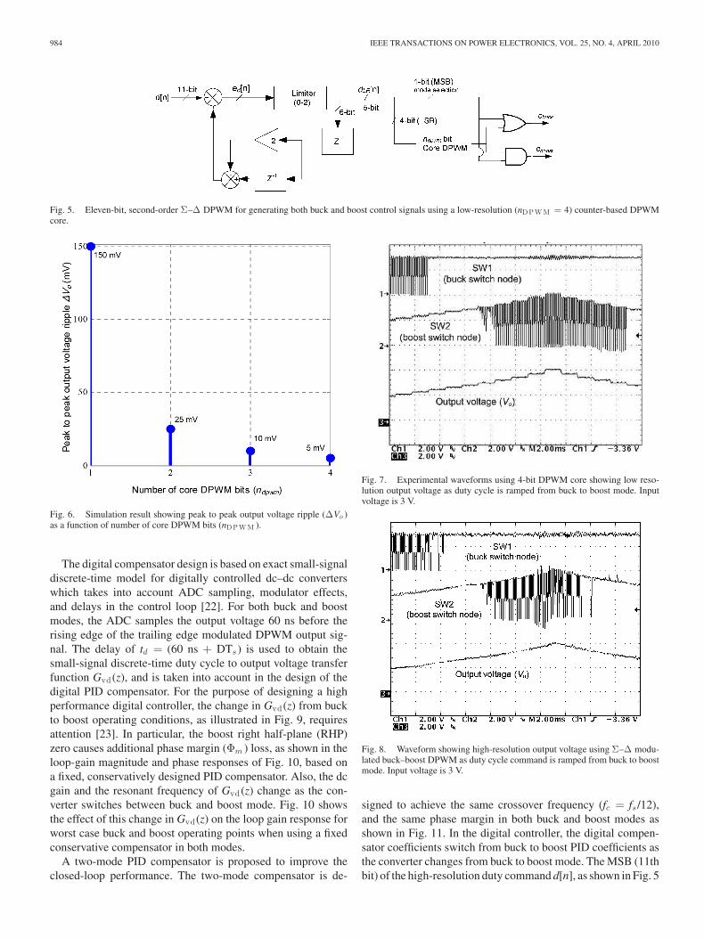
The second-order Σ–∆ DPWM is implemented as shown inFig. 5, which follows the implementation described in [16], butfurther including the ability to generate buck and boost gate-drive control signals cbuck and cboost , respectively. The input tothe Σ–∆ DPWM is a high-resolution 11-bit command d[n] fromthe two-mode PID compensator. The PWM duty cycle commandcbuck and cboost control the power converter switches. The extraoutput voltage ripple produced by the Σ–∆ DPWM comparedto an ideal high-resolution DPWM depends on the number ofbits nDPWM of the core DPWM. Fig. 6 summarizes the outputvoltage ripple as a function of the core DPWM resolution at aworst-case operating point. Note that the ideal output voltageripple with an ideal analog PWM at this operating point is 2 mV.A 4-bit core DPWM is chosen for implementation with the Σ–∆modulator, allowing an effective 11-bit high-resolution duty cy-cle command, as shown in Fig. 5.
In the experimental prototype, the switching frequency is fs =1.56 MHz. The MSB of a 5-bit command dLR to the modulatordecides the mode (buck or boost) of operation. The four LSBsare the duty cycle command to the 4-bit counter-based DPWMcore. The system clock frequency is 24 fs = 25 MHz. In buckmode, for dLR [n] less than or equal to 1, the boost control signalcboost has 0% duty cycle. Hence, referring to Fig. 4, powerswitch S3 is always on and S4 is always off. In boost mode, fordLR [n] greater than or equal to 1, the buck PWM control signalcbuck has 100% duty ratio, power switch S1 is always on andpower switch S2 is always off.
Fig. 7 shows the output voltage and the switch node wave-forms as the command dLR is swept from buck mode to boostmode with no Σ–∆ modulation in front of the DPWM. Thecoarse DPWM resolution, with pulse width steps of 40 ns re-sults in large output voltage steps. In closed-loop operation,resulting limit cycling oscillations would produce unacceptablylarge output voltage ripple, similar to the behavior observedwith analog controllers around the mode transition [13]. Usingthe second-order Σ–∆ modulator in front of the 4-bit DPWMas shown in Fig. 5 enables high-resolution (11-bit) duty cyclecommand d[n]. An experimental sweep of the high-resolutioncommand d is shown in Fig. 8, demonstrating high-resolutionoutput voltage positioning in buck and boost modes.
B. Two-Mode Digital Compensator Design andClosed-Loop Operation
To demonstrate closed-loop operation, the noninvertingbuck–boost power stage is fed with buck and boost PWM pulsescbuck and cboost , generated from a two-mode digital compen-sator as shown in Fig 4. The input voltage Vin is 2.7–5.5 V andthe regulated output voltage can be set between 0.8 and 3.6 Vwith 500 mA maximum load current. The filter components areL = 2.2 µH, C = 10 µF and the switching frequency is fs =1.56 MHz. The voltage sensing A–D converter (ADC) has a32 mV LSB resolution. The digital controller is implementedon an FPGA with 25 MHz system clock frequency.
984 IEEE TRANSACTIONS ON POWER ELECTRONICS, VOL. 25, NO. 4, APRIL 2010
Fig. 5. Eleven-bit, second-order Σ–∆ DPWM for generating both buck and boost control signals using a low-resolution (nDPW M = 4) counter-based DPWMcore.
Fig. 6. Simulation result showing peak to peak output voltage ripple (∆Vo )as a function of number of core DPWM bits (nDPW M ).
The digital compensator design is based on exact small-signaldiscrete-time model for digitally controlled dc–dc converterswhich takes into account ADC sampling, modulator effects,and delays in the control loop [22]. For both buck and boostmodes, the ADC samples the output voltage 60 ns before therising edge of the trailing edge modulated DPWM output sig-nal. The delay of td = (60 ns + DTs) is used to obtain thesmall-signal discrete-time duty cycle to output voltage transferfunction Gvd (z), and is taken into account in the design of thedigital PID compensator. For the purpose of designing a highperformance digital controller, the change in Gvd (z) from buckto boost operating conditions, as illustrated in Fig. 9, requiresattention [23]. In particular, the boost right half-plane (RHP)zero causes additional phase margin (Φm ) loss, as shown in theloop-gain magnitude and phase responses of Fig. 10, based ona fixed, conservatively designed PID compensator. Also, the dcgain and the resonant frequency of Gvd (z) change as the con-verter switches between buck and boost mode. Fig. 10 showsthe effect of this change in Gvd (z) on the loop gain response forworst case buck and boost operating points when using a fixedconservative compensator in both modes.
A two-mode PID compensator is proposed to improve theclosed-loop performance. The two-mode compensator is de-
Fig. 7. Experimental waveforms using 4-bit DPWM core showing low reso-lution output voltage as duty cycle is ramped from buck to boost mode. Inputvoltage is 3 V.
Fig. 8. Waveform showing high-resolution output voltage using Σ–∆ modu-lated buck–boost DPWM as duty cycle command is ramped from buck to boostmode. Input voltage is 3 V.
signed to achieve the same crossover frequency (fc = fs /12),and the same phase margin in both buck and boost modes asshown in Fig. 11. In the digital controller, the digital compen-sator coefficients switch from buck to boost PID coefficients asthe converter changes from buck to boost mode. The MSB (11thbit) of the high-resolution duty command d[n], as shown in Fig. 5

PAUL et al.: POWER MANAGEMENT OF WIDEBAND CODE DIVISION MULTIPLE ACCESS RF POWER AMPLIFIERS WITH ANTENNA MISMATCH 985
Fig. 9. Illustration of differences in control-to-output transfer function Gvd (z)in buck and boost operating modes.
Fig. 10. Illustration of differences in loop gain plot for buck and boost oper-ating modes using a fixed conservative PID compensator. Operating condition1) buck: Vin = 2.7 V, Vo = 0.8 V and Iload = 0 A. 2) Boost: Vin = 2.7 V,Vo = 3.6 V and Iload = 0.5 A. Note the phase-margin loss of Φm = 11.
is used as the control signal (see Pmode in Fig. 4) to switch thetwo-mode PID coefficients between buck and boost PID. Table Isummarizes the improvement in phase margin (Φm ), crossoverfrequency (fc ), and the gain margin (GM) by using the two-modePID compensator compared to the fixed conservative compen-sator.
Fig. 12 shows the hardware realization of the two-mode PID.Note that at steady state, d[n] is fixed if the output voltage iswithin the zero-error bin of the ADC. Hence, either the buckor the boost PID coefficients are selected by the MSB of d[n]command. Also, note that the same hardware is used for bothbuck and boost PID realization and only the coefficients areupdated as selected by the MSB of d[n].
Fig. 11. Loop gain plot for buck and boost operating modes maintainingsimilar phase margin Φm and crossover frequency fc using the two-mode PIDcompensator design.
TABLE ISUMMARY OF SMALL-SIGNAL LOOP GAIN RESPONSES FOR BUCK AND BOOST
MODES USING A FIXED AND TWO-MODE PID COMPENSATOR DESIGN
Fig. 12. Realization of the two-mode PID. The MSB (11th bit) of d[n] se-lects the different PID coefficients K, R1 and R2 to realize buck or boost PIDcompensator.
C. Verification of Smooth Buck–Boost Mode Transition
The experimental setup to verify the closed-loop operation ofthe power converter as shown in Fig. 4 consists of a power stageIC, which is regulated by the Σ–∆ modulated digital controllerimplemented in an FPGA. The power stage IC includes the buck
986 IEEE TRANSACTIONS ON POWER ELECTRONICS, VOL. 25, NO. 4, APRIL 2010
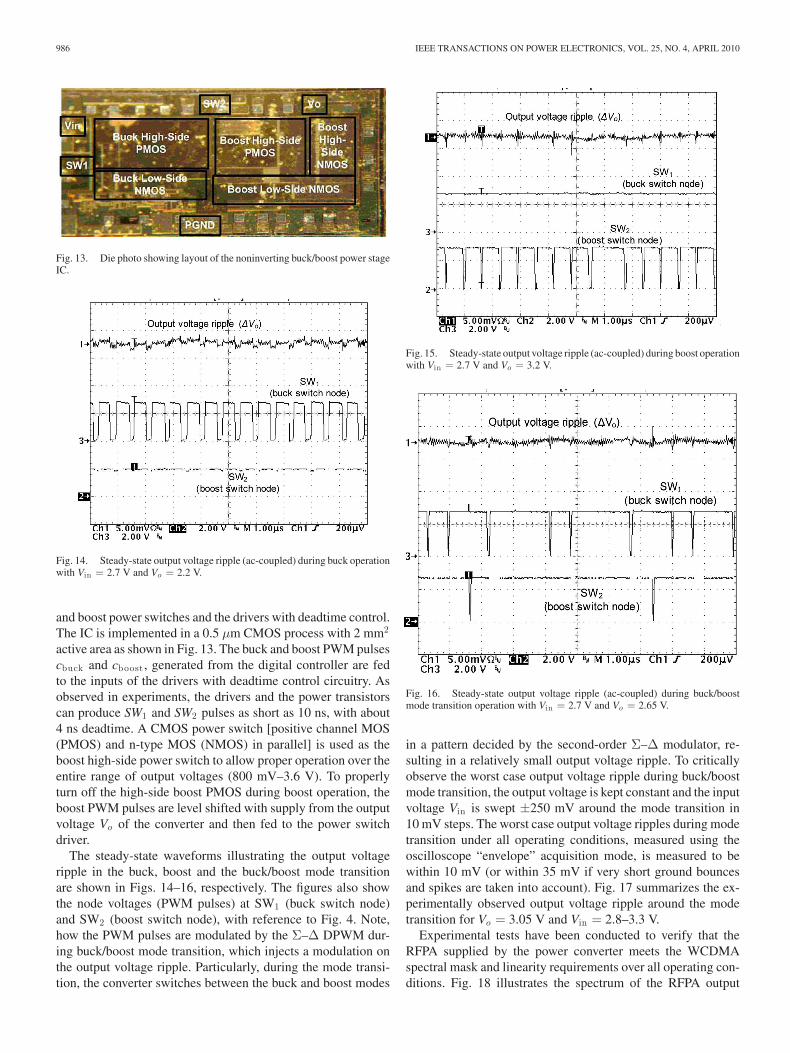
Fig. 13. Die photo showing layout of the noninverting buck/boost power stageIC.
Fig. 14. Steady-state output voltage ripple (ac-coupled) during buck operationwith Vin = 2.7 V and Vo = 2.2 V.
and boost power switches and the drivers with deadtime control.The IC is implemented in a 0.5 µm CMOS process with 2 mm2
active area as shown in Fig. 13. The buck and boost PWM pulsescbuck and cboost , generated from the digital controller are fedto the inputs of the drivers with deadtime control circuitry. Asobserved in experiments, the drivers and the power transistorscan produce SW1 and SW2 pulses as short as 10 ns, with about4 ns deadtime. A CMOS power switch [positive channel MOS(PMOS) and n-type MOS (NMOS) in parallel] is used as theboost high-side power switch to allow proper operation over theentire range of output voltages (800 mV–3.6 V). To properlyturn off the high-side boost PMOS during boost operation, theboost PWM pulses are level shifted with supply from the outputvoltage Vo of the converter and then fed to the power switchdriver.
The steady-state waveforms illustrating the output voltageripple in the buck, boost and the buck/boost mode transitionare shown in Figs. 14–16, respectively. The figures also showthe node voltages (PWM pulses) at SW1 (buck switch node)and SW2 (boost switch node), with reference to Fig. 4. Note,how the PWM pulses are modulated by the Σ–∆ DPWM dur-ing buck/boost mode transition, which injects a modulation onthe output voltage ripple. Particularly, during the mode transi-tion, the converter switches between the buck and boost modes
Fig. 15. Steady-state output voltage ripple (ac-coupled) during boost operationwith Vin = 2.7 V and Vo = 3.2 V.
Fig. 16. Steady-state output voltage ripple (ac-coupled) during buck/boostmode transition operation with Vin = 2.7 V and Vo = 2.65 V.
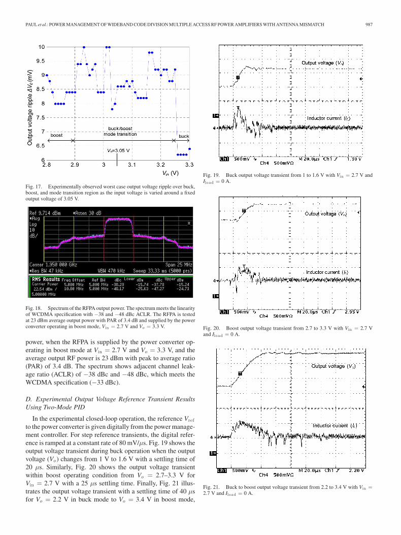
in a pattern decided by the second-order Σ–∆ modulator, re-sulting in a relatively small output voltage ripple. To criticallyobserve the worst case output voltage ripple during buck/boostmode transition, the output voltage is kept constant and the inputvoltage Vin is swept ±250 mV around the mode transition in10 mV steps. The worst case output voltage ripples during modetransition under all operating conditions, measured using theoscilloscope “envelope” acquisition mode, is measured to bewithin 10 mV (or within 35 mV if very short ground bouncesand spikes are taken into account). Fig. 17 summarizes the ex-perimentally observed output voltage ripple around the modetransition for Vo = 3.05 V and Vin = 2.8–3.3 V.
Experimental tests have been conducted to verify that theRFPA supplied by the power converter meets the WCDMAspectral mask and linearity requirements over all operating con-ditions. Fig. 18 illustrates the spectrum of the RFPA output
PAUL et al.: POWER MANAGEMENT OF WIDEBAND CODE DIVISION MULTIPLE ACCESS RF POWER AMPLIFIERS WITH ANTENNA MISMATCH 987
Fig. 17. Experimentally observed worst case output voltage ripple over buck,boost, and mode transition region as the input voltage is varied around a fixedoutput voltage of 3.05 V.
Fig. 18. Spectrum of the RFPA output power. The spectrum meets the linearityof WCDMA specification with −38 and −48 dBc ACLR. The RFPA is testedat 23 dBm average output power with PAR of 3.4 dB and supplied by the powerconverter operating in boost mode, Vin = 2.7 V and Vo = 3.3 V.
power, when the RFPA is supplied by the power converter op-erating in boost mode at Vin = 2.7 V and Vo = 3.3 V, and theaverage output RF power is 23 dBm with peak to average ratio(PAR) of 3.4 dB. The spectrum shows adjacent channel leak-age ratio (ACLR) of −38 dBc and −48 dBc, which meets theWCDMA specification (−33 dBc).
D. Experimental Output Voltage Reference Transient ResultsUsing Two-Mode PID
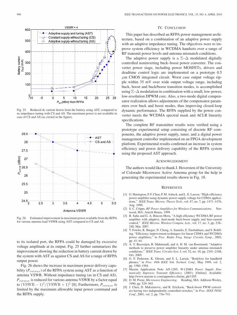
In the experimental closed-loop operation, the reference Vrefto the power converter is given digitally from the power manage-ment controller. For step reference transients, the digital refer-ence is ramped at a constant rate of 80 mV/µs. Fig. 19 shows theoutput voltage transient during buck operation when the outputvoltage (Vo ) changes from 1 V to 1.6 V with a settling time of20 µs. Similarly, Fig. 20 shows the output voltage transientwithin boost operating condition from Vo = 2.7–3.3 V forVin = 2.7 V with a 25 µs settling time. Finally, Fig. 21 illus-trates the output voltage transient with a settling time of 40 µsfor Vo = 2.2 V in buck mode to Vo = 3.4 V in boost mode,
Fig. 19. Buck output voltage transient from 1 to 1.6 V with Vin = 2.7 V andIload = 0 A.
Fig. 20. Boost output voltage transient from 2.7 to 3.3 V with Vin = 2.7 Vand Iload = 0 A.
Fig. 21. Buck to boost output voltage transient from 2.2 to 3.4 V with Vin =2.7 V and Iload = 0 A.

988 IEEE TRANSACTIONS ON POWER ELECTRONICS, VOL. 25, NO. 4, APRIL 2010
Fig. 22. Experimental setup for closed-loop adaptive supply and impedance tuning for WCDMA RFPA transmitter system.
with Vin = 2.7 V. The two-mode controller adaptively switchesthe compensator coefficients from buck PID to boost PID as itchanges from buck to boost operating mode. An advantage ofusing the two-mode compensator is that the output voltage canbe positioned with improved performances in terms of settlingtime and damping.
III. ADAPTIVE RFPA SUPPLY AND IMPEDANCE
TUNING SYSTEM
Fig. 22 shows a block diagram of the setup for experimentalverification of the proposed AST power management architec-ture. A directional coupler senses the RF output power of theRFPA and the RF power reflected by the antenna. Any mis-match at the antenna produces a signal VVSWR at the output ofthe gain detector. This signal is digitized and fed to the powermanagement controller, which is implemented on an FPGA de-velopment platform, and includes both the buck–boost powerconverter control as described in Section II, and the tuner con-trol. The tuner controller adjusts the matching network to mini-mize the reflected power and VSWR, while the power controlleradjusts the RFPA power supply so as to preserve linearity. Withthis architecture, the reflected power from the antenna is not lostas in the standard configuration with the isolator (see Fig. 1),thus improving overall system efficiency. Another important
role of the tuner is to protect the PA from power reflected bythe antenna. Furthermore, the adaptive impedance tuner allowsthe RFPA supply to be minimized, increase the overall systemefficiency.
Fig. 22 shows the RFPA used in the experiment is an AvagoWS2512 with maximum output power Pmax = 28 dBm between1.92–1.98 GHz. The surface mount 20 dB bidirectional couplerhas 40 dB isolation. The power management controller is imple-mented in Xilinx Virtex 4 XC4VLX25 FPGA. It samples real-time antenna mismatch parameter VSWR (VVSWR ) detected bythe coupler and AD8302 gain detector. The antenna is mod-eled by a variable impedance load from Focus Microwave. Thedigitized detector output VVSWR is used by the two functionalblocks: the tuner controller to adjust the impedance networkand the RFPA power supply controller, which adjusts the Vrefcommand. Finally, Vref sets the RFPA supply Vo , which is reg-ulated by the power controller. Under mismatched antenna loadcondition, which is detected from VVSWR magnitude, the RFPAsupply is increased to 3.3 V by adjusting the Vref command.After the tuner causes a matched condition, Vref is set to theminimum value to supply optimum dc voltage to the PA de-pending on the input RF power command. The optimum Vrefcommand is stored in a lookup table, which is obtained aftercharacterizing the minimum supply requirement of the RFPA atless than 0.5 dB compression point.

PAUL et al.: POWER MANAGEMENT OF WIDEBAND CODE DIVISION MULTIPLE ACCESS RF POWER AMPLIFIERS WITH ANTENNA MISMATCH 989
Fig. 23. Circuit diagram shows the double-stub tuner with a varactor diodeat the end of the two shunt stubs. The tuner provides an input port impedance(Zin ) with VSWR < 1.5 at 1.95 GHz for antenna loads (ZL ) with mismatch upto VSWR = 5.5.
A. RF Impedance Tuner
The impedance matching network design chosen for this workis a double-stub architecture with two varactor diodes (Sky-works 1405), as shown in Fig. 23. The tuner provides an inputport impedance (Zin ) with VSWR < 1.5 at 1.95 GHz for an-tenna loads (ZL ) with mismatch up to VSWR = 5.5. The tunerexhibits insertion loss as low as 0.3 dB and uses two separatecontrol voltages V1 and V2 between 0 and 5 V. The optimumvaractor bias voltages are determined by connecting the tuner toknown loads and then searching for the tuner state that results inthe least reflected power (minimum VSWR), and the resultinglookup table of voltages is loaded in the power managementcontroller. Thus during closed-loop operation of the system, thetuner controller as shown in Fig. 22 searches the best combi-nation of tuner control voltages from a precalibrated lookuptable to minimize antenna reflected power. Further details of theimplementation of the RF impedance tuner are given in [24].
B. Efficiency Improvement Using Adaptive Supply WithImpedance Tuning Compared to Constant Supply Without Tun-ing (CS) and Adaptive Supply Without Tuning (AS)
The experimental setup as shown in Fig. 22 is used to comparethe improvement in power added efficiency (PAE) and the outputpower delivery capability (Pout) of the RFPA system. Threedifferent system approaches are studied to compare the results:the proposed AST architecture, against CS and AS. As describedearlier, for AST, the RFPA supply is adaptively adjusted fromthe power management controller, depending on the RF powertransmit level and the antenna VSWR condition. For CS, thesupply to the PA is a constant 3.3 V. For AS, the RFPA supply
Fig. 24. Improvement in efficiency using AST compared to CS and AS powermanagement architectures. Antenna load results in VSWR = 4. Note that thereis an improvement in maximum power delivery capability of the RFPA by 2 dB(circled).
is only adjusted as a function of the requested power transmitlevel. PAE is given by
PAE =Pout − Pin
Pdc
where Pout and Pin are the output and input RF power of theRFPA and Pdc is the dc power consumption. The RF power Poutis found from the RFPA gain (G), tuned VSWR from the VSWRdetector, and characterized tuner loss (TL) in the varactor-basedtuner as
Pout = Pin + G − TL. (1)
DC power consumption Pdc includes losses in the power con-verter stage, and 20 mA of quiescent current consumption ofthe AD8302 gain detector. The digital power management con-troller, including ADC and D–A converter (DAC) interfaces,could easily be implemented on a digital baseband chip, withnegligible power consumption, which is why the controllerpower consumption is not included in Pdc . Based on cell phoneantenna measurements, the antenna VSWR is expected to be ashigh as 4 [24]. The tuner loss TL is reported in [24] for variousVSWR values.
Fig. 24 shows the improvement in efficiency of the system forantenna load VSWR = 4 (with phase at 0 for maximum collectorvoltage swing [5]). Simultaneous improvement in the maximumpower available, and efficiency from the RFPA is obtained us-ing the proposed AST approach. Note that, this improvementwith AST is due to simultaneous reduction in antenna reflectedpower and allows lower supply voltage and drawn battery cur-rent. Furthermore, the dc power consumption, Pdc is higher forCS and AS than in AST, since the required RFPA supply volt-age is higher so as to restrict the RFPA saturation during highVSWR load. In both CS and AS, the reflected power is lost.Furthermore, without the isolator to divert the reflected power
990 IEEE TRANSACTIONS ON POWER ELECTRONICS, VOL. 25, NO. 4, APRIL 2010
Fig. 25. Reduced dc current drawn from the battery using AST, compared tono impedance tuning with CS and AS. The maximum power is not available incase of CS and AS (as circled in the figure).
Fig. 26. Estimated improvement in maximum power available from the RFPAfor various antenna load VSWR using AST compared to CS and AS.
to its isolated port, the RFPA could be damaged by excessivevoltage amplitude at its output. Fig. 25 further summarizes theimprovement showing the reduction in battery current drawn bythe system with AST as against CS and AS for a range of RFPAoutput power.
Fig. 26 shows the increase in maximum power delivery capa-bility (Poutmax) of the RFPA system using AST as a function ofantenna VSWR. Without impedance tuning (as in CS and AS),Poutmax is reduced for various antenna VSWR by a factor equalto (VSWR − 1)2/(VSWR + 1)2 [8]. Furthermore, Poutmax islimited by the maximum allowable input power command andthe RFPA supply.
IV. CONCLUSION
This paper has described an RFPA power management archi-tecture, based on a combination of an adaptive power supplywith an adaptive impedance tuning. The objectives were to im-prove system efficiency in WCDMA handsets over a range ofRF transmit power levels and antenna mismatch conditions.
The adaptive power supply is a Σ–∆ modulated digitallycontrolled noninverting buck–boost power converter. The con-verter power stage, including power MOSFETs, drivers anddeadtime control logic are implemented on a prototype 0.5µm CMOS integrated circuit. Worst case output voltage rip-ple within 35 mV over wide output voltage range, includingbuck, boost and buck/boost transition modes, is accomplishedusing Σ–∆ modulation in combination with a small, low-power,low-resolution DPWM core. Also, a two-mode digital compen-sator realization allows adjustments of the compensator param-eters over buck and boost modes, thus improving closed-loopdynamic performance. The RFPA supplied by the power con-verter meets the WCDMA spectral mask and ACLR linearityspecifications.
The complete RF transmitter results were verified using aprototype experimental setup consisting of discrete RF com-ponents, the adaptive power supply, tuner, and a digital powermanagement controller implemented on an FPGA developmentplatform. Experimental results confirmed an increase in systemefficiency and power delivery capability of the RFPA systemusing the proposed AST approach.
ACKNOWLEDGMENT
The authors would like to thank J. Hoversten of the Universityof Colorado Microwave Active Antenna group for the help ingenerating the experimental results shown in Fig. 18.
REFERENCES
[1] G. Hanington, P. F. Chen, P. M. Asbeck, and L. E. Larson, “High-efficiencypower amplifier using dynamic power-supply voltage for CDMA applica-tions,” IEEE Trans. Microw. Theory Tech., vol. 47, no. 7, pp. 1471–1476,Aug. 1999.
[2] S. C. Cripps, RF Power Amplifiers for Wireless Communications. Nor-wood, MA: Artech House, 1999.
[3] B. Sahu and G. A. Rincon-Mora, “A high efficiency WCDMA RF poweramplifier with adaptive, dual-mode buck-boost supply and bias-currentcontrol,” IEEE Microw. Wireless Compon. Lett., vol. 17, no. 3, pp. 238–240, Mar. 2007.
[4] T. Fowler, K. Burger, N. Cheng, A. Samelis, E. Enobakhare, and S. Rohlf-ing, “Efficiency improvement techniques for linear CDMA and WCDMApower amplifiers,” in Proc. Radio Freq. Integr. Circuits Symp., 2002,pp. 41–44.
[5] A. V. Bezooijen, R. Mahmoudi, and A. H. M. van Roermund, “Adaptivemethods to preserve power amplifier linearity under antenna mismatchconditions,” IEEE Trans. Circuits Syst. I, vol. 52, no. 10, pp. 2101–2108,Oct. 2005.
[6] G. F. Pedersen, K. Olesen, and S. L. Larsen, “Bodyloss for handheldphones,” in Proc. 49th IEEE Veh. Technol. Conf., May 1999, vol. 2,pp. 1580–1584.
[7] Maxim Application Note AN-1205, W-CDMA Power Supply Dra-matically Improves Transmit Efficiency. (2001). [Online]. Available:http://www.maxim-ic.com/appnotes.cfm/an_pk/1205
[8] D. M. Pozar, Microwave Engineering. Reading, MA: Addison-Wesley,1990, pp. 529–565.
[9] J. Chen, D. Maksimovic, and R. Erickson, “Buck-boost PWM convert-ers having two independently controlled switches,” in Proc. IEEE PESCConf., 2001, vol. 2, pp. 736–741.

PAUL et al.: POWER MANAGEMENT OF WIDEBAND CODE DIVISION MULTIPLE ACCESS RF POWER AMPLIFIERS WITH ANTENNA MISMATCH 991
[10] M. Gaboriault and A. Notman, “A high efficiency, non-inverting, buck-boost DC–DC converter,” in Proc. IEEE APEC Conf., 2004, vol. 3,pp. 1411–1415.
[11] P. Midya, K. Haddad, and M. Miller, “Buck or boost tracking powerconverter,” IEEE Power Electron. Lett., vol. 2, no. 4, pp. 131–134, Dec.2004.
[12] A. Prodic and D. Maksimovic, “Digital PWM controller and current es-timator for a low-power switching converter,” in Proc. IEEE COMPELConf., 2000, pp. 123–128.
[13] R. Paul and D. Maksimovic, “Analysis of PWM nonlinearity in non-inverting buck-boost power converters,” in Proc. IEEE PESC Conf., 2008,pp. 3741–3747.
[14] Y. J. Lee, A. Khaligh, and A. Emadi, “A compensation technique forsmooth transitions in a non-inverting buck-boost converter,” IEEE Trans.Power Electron., vol. 24, no. 4, pp. 1002–1015, Apr. 2009.
[15] F. H. Raab, P. Asbeck, S. Cripps, P. B. Kenington, Z. B. Popovic, N. Pothe-cary, J. F. Sevic, and N. O. Sokal, “Power amplifiers and transmitters forRF and microwave,” IEEE Trans. Microw. Theory Tech., vol. 50, no. 3,pp. 814–826, Mar. 2002.
[16] Z. Lukic, N. Rahman, and A. Prodic, “Multibit Σ-∆ PWM digital con-troller IC for DC–DC converters operating at switching frequencies be-yond 10 MHz,” IEEE Trans. Power Electron., vol. 22, no. 5, pp. 1693–1707, Sep. 2007.
[17] R. Paul, L. Corradini, and D. Maksimovic, “Σ-∆ modulated digitallycontrolled non-inverting buck-boost converter for WCDMA RF poweramplifiers,” in Proc. IEEE APEC Conf., 2009, pp. 533–539.
[18] A. Syed, E. Ahmed, D. Maksimovic, and E. Alarcon, “Digital pulse widthmodulator architectures,” in Proc. IEEE PESC Conf., 2004, pp. 4689–4695.
[19] A. V. Peterchev and S. R. Sanders, “Quantization resolution and limitcycling in digitally controlled PWM converters,” IEEE Trans. PowerElectron., vol. 18, no. 1, pp. 301–308, Jan. 2003 [Special Issue on DigitalControl].
[20] H. Peng, A. Prodic, E. Alarcon, and D. Maksimovic, “Modeling of quan-tization effects in digitally controlled dc–dc converters,” IEEE Trans.Power Electron., vol. 22, no. 1, pp. 208–215, Jan. 2007.
[21] M. Norris, L. Marco, E. Alarcon, and D. Maksimovic, “Quantization noiseshaping in digital PWM converters,” in Proc. IEEE PESC Conf., 2008,pp. 127–133.
[22] D. Maksimovic and R. Zane, “Small-signal discrete-time modeling ofdigitally controlled PWM converters,” IEEE Trans. Power Electron.,vol. 22, no. 6, pp. 2552–2556, Nov. 2007.
[23] R. W. Erickson and D. Maksimovic, Fundamentals of Power Electronics,2nd ed. Boston, MA: Kluwer, 2000, pp. 265–322.
[24] L. Sankey and Z. Popovic, “Adaptive tuning of handheld transmitters,” inProc. IEEE MTT-S IMS Dig., Jun. 2009, pp. 225–228.
Rajarshi Paul (S’05) received the B.Tech. de-gree from the Indian Institute of Technology (IIT),Kharagpur, India, in 2003, and the M.S. degrees inelectrical engineering from IIT, Kharagpur and Uni-versity of Colorado, Boulder, in 2008. He is currentlyworking toward the Ph.D. degree with the Universityof Colorado.
From 2004 to 2006, he was a Graduate ResearchConsultant at Advanced VLSI Design Laboratory,IIT, Kharagpur. Since 2006, he has been a GraduateResearch Assistant with Colorado Power Electronics
Center, University of Colorado. In summer 2007, he was a Circuit Design In-tern with National Semiconductor. His current research interests include powermanagement integrated circuits, high-speed analog and mixed-signal IC, RF,and system on chip design.
Luke Sankey (S’99) received the B.S.E.E. degree from the Seattle PacificUniversity, Seattle, WA, in 2001, and the M.E.E.E. degree in 2007 from theUniversity of Colorado, Boulder, where he is currently working toward thePh.D. degree and where he has been engaged in research on the adaptive controlof tunable RF elements.
From 2001 to 2005, he was with Honeywell Aerospace for five years, writingsoftware for their commercial weather radar products. His current researchinterest includes embedded RF systems.
Luca Corradini (S’06– M’09) received the Laureadegree in electronic engineering, and the Ph.D. de-gree in information engineering from the Universityof Padova, Padua, Italy, in 2004 and 2008, respec-tively.
He is currently a Postdoctoral Research Associateat the Colorado Power Electronics Center, Univer-sity of Colorado, Boulder. His research interests inpower electronics are primarily focused on the devel-opment and modeling of digital control techniquesfor switched-mode power converters, including the
study of high-sampling frequency regulators as well as the development ofautotuning techniques for automated online self-compensation of digitally con-trolled SMPS.
Dr. Corradini received the second 2008 Prize Paper Award from the IndustrialPower Converter Committee of the IEEE Industry Applications Society.
Zoya Popovic (S’86–M’90–SM’99–F’02) receivedthe Dipl.Ing. degree from the University of Bel-grade, Serbia, in 1985, and the Ph.D. degree from theCalifornia Institute of Technology, Pasadena, in 1990.
Since 1990, she has been with the University ofColorado, Boulder, where she is currently the HudsonMoore, Jr., Chaired Professor in the Department ofElectrical, Computer and Energy Engineering. In2001, she was a Visiting Professor with the Tech-nical University of Munich, Munich. Since 1991, shehas guided 34 Ph.D. students and currently advises a
group of 15 graduate students. Her research interests include high-efficiency,low-noise and broadband microwave and millimeter-wave circuits, quasi-opticalmillimeter-wave techniques for imaging, smart and multibeam antenna arrays,intelligent RF front ends, RF optics, and wireless powering for batterylesssensors.
Dr. Popovic is currently an Associate Editor for the IEEE TRANSACTIONS
ON MICROWAVE THEORY AND TECHNIQUES. She was the recipient of the 1993and 2006 Microwave Prizes presented by the IEEE Microwave Theory andTechniques Society for the best journal papers, and received the 1996 URSIIssacKoga Gold Medal. In 1997, Eta Kappa Nu students chose her as a Profes-sor of the Year. She was the recipient of a 2000 Humboldt Research Award forSenior U.S. Scientists from the German Alexander von Humboldt Stiftung.She was also the recipient of the 2001 Hewlett-Packard/American Societyfor Engineering Education Terman Medal for combined teaching and researchexcellence.
Dragan Maksimovic (M’89–SM’04) received theB.S. and M.S. degrees in electrical engineering fromthe University of Belgrade, Belgrade, Yugoslavia,in 1984 and 1986, respectively, and the Ph.D. de-gree from the California Institute of Technology,Pasadena, in 1989.
From 1989 to 1992, he was with the Universityof Belgrade. Since 1992, he has been with the De-partment of Electrical, Computer and Energy Engi-neering, University of Colorado, Boulder, where he iscurrently a Professor and the Director of the Colorado
Power Electronics Center. His current research interests include digital controltechniques and mixed-signal integrated circuit design for power electronics.
Dr. Maksimovic received the 1997 NSF CAREER Award, the Power Elec-tronics Society Transactions Prize Paper Award in 1997 and 2008, respectively,the Bruce Holland Excellence in Teaching Award in 2004, and the Universityof Colorado Inventor of the Year Award in 2006. He is currently an AssociateEditor for the IEEE TRANSACTIONS ON POWER ELECTRONICS.