ieee transactions on power electronics, vol 00, no 00
TRANSCRIPT
0885-8993 (c) 2015 IEEE. Personal use is permitted, but republication/redistribution requires IEEE permission. See http://www.ieee.org/publications_standards/publications/rights/index.html for more information.
This article has been accepted for publication in a future issue of this journal, but has not been fully edited. Content may change prior to final publication. Citation information: DOI 10.1109/TPEL.2016.2523121, IEEETransactions on Power Electronics
IEEE TRANSACTIONS ON POWER ELECTRONICS, VOL 00, NO 00, JULY 2015 1
Design of Maximum Efficiency Tracking ControlScheme for Closed Loop Wireless Power Charging
System Employing Series Resonant TankTae-Dong Yeo, DukSoo Kwon, Seung-Tae Khang and Jong-Won Yu, Member, IEEE
Abstract—This paper presents a maximum efficiency trackingcontrol scheme for a closed-loop wireless power charging (WPC)system for wireless charging of mobile devices. Generally, wirelesscharging systems need precise output voltage and current withthe highest possible efficiency. In an open-loop system, outputvoltage and efficiency depend strongly on the coupling coefficientand load condition. Alternatively, a closed-loop WPC system hasa constant output voltage against coupling and load variations.Many studies have been carried out regarding closed-loop sys-tems. However, those previous studies have the drawback ofefficiency degradation. In this paper, we propose a maximumefficiency tracking (MET) control scheme to achieve the highestpossible efficiency. Therefore, the proposed WPC system satisfiesboth the requirements of a constant output voltage and highefficiency. The proposed control scheme determines the currentof the transmitter based on the data received by the receivervia bluetooth. For validation, the proposed WPC system wasimplemented at 6.78 MHz using loosely coupled series-seriesresonant coils, and we verified that the proposed system can trackthe maximum efficiency while maintaining a constant outputvoltage.
Keywords—Wireless power transfer, Wireless power charging,Maximum efficiency tracking control scheme, Variable load, Opti-mization load, Closed loop system.
I. INTRODUCTION
W ITH the growing demand for charging of wearabledevices and Internet of Things (IoT) devices anywhere
without wires, wireless power transfer (WPT) has been studied.Therefore, in recent years, most research in this area hasfocused on high efficiency and long charging distance [1]-[3], but it is just concerned with transferring energy. However,many real industrial and commercial applications must providea precise output voltage with the highest possible efficiency.Unfortunately, output voltage and efficiency vary with thecoupling coefficient and load conditions in an open-loopWPT system. Additionally, the coupling coefficient and loadconditions vary in relation to the environment. For instance,during the charging of a smart phone, the load conditionschange because the charging battery, and coupling coefficientis changed by the position of the smart phone. Therefore, in
Tae-Dong Yeo, DukSoo Kwon, Seung-Tae Khang, and Jong-Won Yuare with the School of Electrical Engineering, Korea Advanced Instituteof Science and Technology (KAIST), Daejeon, Republic of Korea (e-mail:[email protected]).
Color versions of one or more of the figures in this paper are availableonline at http://ieeexplore.ieee.org.
this paper, the proposed WPC system is intended to satisfythe requirements for both a constant output voltage and highefficiency.
To provide a constant output voltage, the design of theproposed WPC system was based on a postregulation closed-loop system, which is among the studied closed-loop regulationmethods. There are three types of closed-loop regulationmethods: frequency tracking, impedance matching, and dc/dcconversion. In frequency tracking methods, the frequency isadjusted in the “over coupled” region, because of the frequencysplit phenomenon to regulate the constant output voltage [2],[4], [5]. In the proposed WPC system, there is no necessityfor frequency tracking because it is a loosely coupled system.In impedance matching methods, the resonant capacitor isregulated by relays or semiconductor switches at a fixedfrequency [6], [7], [12]. Thus, it can regulate the output voltageby changing impedance and constant output voltage can alsobe maintained, but the impedance matching circuit is complexand has a loss, and control is difficult. The last type of methoduses a dc/dc converter in the receiving or transmitting side [8].It is a simple structure to provide a constant output voltage.When such a system is applied to closed-loop regulation,it degrades system efficiency because the equivalent loadimpedance deviates from the optimal point; however, efficiencycan be improved by the proposed maximum efficiency trackingcontrol scheme.
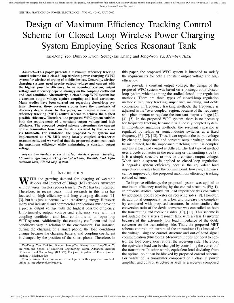
To improve efficiency, the proposed system was applied tomaximum efficiency tracking by the control structure (Fig 1).In previous studies, equivalent load impedance was controlledby additional boost converter on receiving sides [9]. However,its additional component has a loss and increase the complex-ity compared with proposed structure. In other studies, theconversion ratio of the dc/dc converter was controlled on boththe transmitting and receiving sides [10], [11]. This scheme isnot suitable for a series resonant tank with a class D inverterbecause of the extremely low load impedance of the dc/dcconverter on the transmitting side. Thus, the proposed METscheme controls the current of the transmitter (IT ) instead ofthe voltage using the control structure and out-of-band signalcommunication (bluetooth). Moreover, it does not need to con-trol the load conversion ratio at the receiving side. Therefore,the equivalent load can be changed by controlling the current ofthe transmitter. In other words, equivalent load deviating fromthe optimal point can be blocked by proposed control scheme.For validation, a transmitter composed of a class D poweramplifier and control structure as well as a receiver composed
0885-8993 (c) 2015 IEEE. Personal use is permitted, but republication/redistribution requires IEEE permission. See http://www.ieee.org/publications_standards/publications/rights/index.html for more information.
This article has been accepted for publication in a future issue of this journal, but has not been fully edited. Content may change prior to final publication. Citation information: DOI 10.1109/TPEL.2016.2523121, IEEETransactions on Power Electronics
IEEE TRANSACTIONS ON POWER ELECTRONICS, VOL 00, NO 00, JULY 2015 2
Fig. 1. Concept of proposed closed loop loosely coupled wireless power charging system : Class D amplifier, control structure, series resonat coil, adaptivereceiver and bluetooth low energy.
of a full bridge rectifier and dc-dc converter were implementedat 6.78 MHz. Transmitting and receiving coils were printed onan FR4 substrate in the A4WP specific. The results of end-to-end measurement (system efficiency (ηsystem) Fig 1.) fromthe dc power amplifier to the dc load showed that maximumefficiency was maintained at every distance. Wherever thereare receivers or whatever receiver has load condition, it can becharged with maximum efficiency.
The remains of this paper is organized as follows. Section IIintroduces closed-loop systems and analyzes the output voltageand efficiency. Then, in section III, we introduce the maximumefficiency tracking control scheme, and in Section IV, wepresent the design of the transmitter and receiver. SectionV verifies the performance of the MET control scheme andpresents the measured results. Finally, this paper concludeswith a short summary in section VI.
II. CLOSED LOOP WIRELESS POWER CHARGING SYSTEM
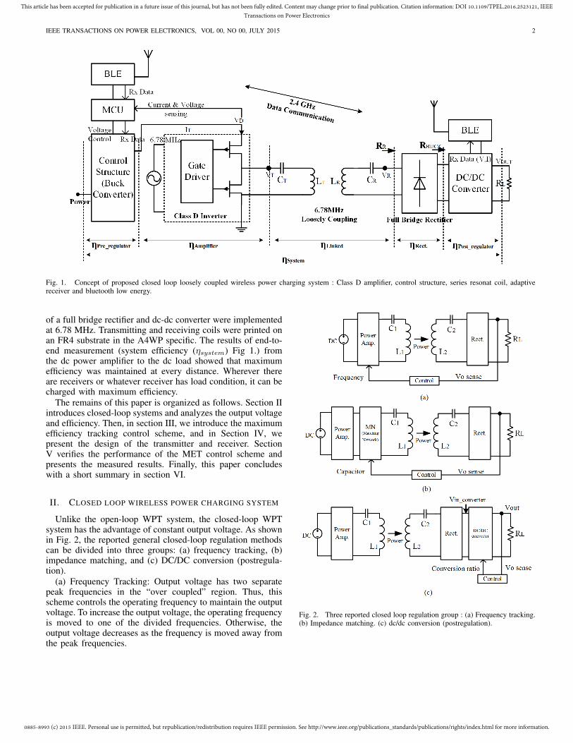
Unlike the open-loop WPT system, the closed-loop WPTsystem has the advantage of constant output voltage. As shownin Fig. 2, the reported general closed-loop regulation methodscan be divided into three groups: (a) frequency tracking, (b)impedance matching, and (c) DC/DC conversion (postregula-tion).
(a) Frequency Tracking: Output voltage has two separatepeak frequencies in the “over coupled” region. Thus, thisscheme controls the operating frequency to maintain the outputvoltage. To increase the output voltage, the operating frequencyis moved to one of the divided frequencies. Otherwise, theoutput voltage decreases as the frequency is moved away fromthe peak frequencies.
Fig. 2. Three reported closed loop regulation group : (a) Frequency tracking.(b) Impedance matching. (c) dc/dc conversion (postregulation).

0885-8993 (c) 2015 IEEE. Personal use is permitted, but republication/redistribution requires IEEE permission. See http://www.ieee.org/publications_standards/publications/rights/index.html for more information.
This article has been accepted for publication in a future issue of this journal, but has not been fully edited. Content may change prior to final publication. Citation information: DOI 10.1109/TPEL.2016.2523121, IEEETransactions on Power Electronics
IEEE TRANSACTIONS ON POWER ELECTRONICS, VOL 00, NO 00, JULY 2015 3
Fig. 3. Equivalent circuit of proposed wireless power charging system.
(b) Impedance Matching: This scheme controls the valueof the capacitors by using relays or semiconductor switches.The value of the capacitors changes the output voltage. With amismatch of the impedance between the power amplifier andload, the output voltage decreases.
(c) DC/DC Conversion (postregulation): Without changingthe operating frequency, the output voltage can be regulatedby a DC/DC converter. The conversion ratio is given by
Cload =Vout
Vin,converter(1)
where Vin,converter is the input voltage of the DC/DCconverter. According to the input voltage, the output voltagecan be maintained by varying the conversion ratio. The fixedoperating frequency of the loosely coupled system does notrequire the frequency tracking scheme. Also, the impedancematching scheme has matching loss and a complicatedmatching network. Therefore, the proposed system waschosen for DC/DC conversion regulation. Although theclosed-loop regulation method can provide a constant outputvoltage, it degrades system efficiency. To compensate thedecrease, the system efficiency of the closed-loop WPCsystem should be improved.
III. PROPOSED MAXIMUM EFFICIENCY TRACKINGCONTROL SCHEME
A. Analysis of proposed WPC systemFig. 3 shows the simplified equivalent circuit of the proposed
WPC system. Loosely coupled coils are in different sizes andshapes, but they share the same resonant frequency.
w0 =1√
LTCT
=1√
LRCR
(2)
Its linked efficiency1 is the function of the coupling coeffi-cient and load impedance, and the efficiency of the proposedsystem is driven by,
ηLinked =PR
PT=
LRk2RR
(RLR +RR) (RLTCT (RLR +RR) + LRk2)(3)
The efficiency (ηLinked) depends on the coupling coefficient(k) and the equivalent load impedance (RR). As mentioned
1Linked efficiency is an efficiency between transmitter coils to receiver coil
Fig. 4. Linked efficiency according to equivalent load impedance andcoupling coefficent.
in section II, because the proposed closed-loop WPC systemis chosen as the postregualtion method, the equivalent loadimpedance (RR) is varied by the Vin,converter. The equivalentload impedance (RR) is given by
RR =RL
C2load
=RL(
Vout
Vin,coverter
)2 =RLV
2in,coverter
V 2out
(4)
where RL is the load impedance (ratio of charging current tovoltage), and Vout is the precise charging voltage. Therefore,the linked efficiency decreases because the DC/DC converterregulates the output voltage. The linked efficiency of a functionof the equivalent load impedance and the coupling coefficientwas calculated and the results are plotted in Fig. 4. As seen inthe figure, the linked efficiency is changed by the equivalentload impedance and the coupling coefficient, and the equivalentload impedance has an optimal point.
B. A principle of the proposed MET control schemeIn a previous study [11], the drain voltage of an amplifier
was controlled by the controller, but the method is not suitablefor a series resonant tank because the input impedance towardthe receiver (Rin) is very low at the operating frequency. Ifthe drain voltage is high, the current of the amplifier wouldbe extremely high, and this would cause critical damage toamplifier. Therefore, the drain voltage of the amplifier (VD)cannot reach the desired value, and the voltage-controlledmethod is not suitable. For this reason, we propose the METcontrol scheme which can control current.
To improve the efficiency degradation associated withclosed-loop regulation, we need to control the coupling co-efficient and the equivalent load impedance from equation(3). First, the coupling coefficient changes in relation to theposition of the receiver, so we cannot control it. Second,from equation (4), the equivalent load impedance is regulatedby the input voltage of the DC/DC converter (Vin,converter).

0885-8993 (c) 2015 IEEE. Personal use is permitted, but republication/redistribution requires IEEE permission. See http://www.ieee.org/publications_standards/publications/rights/index.html for more information.
This article has been accepted for publication in a future issue of this journal, but has not been fully edited. Content may change prior to final publication. Citation information: DOI 10.1109/TPEL.2016.2523121, IEEETransactions on Power Electronics
IEEE TRANSACTIONS ON POWER ELECTRONICS, VOL 00, NO 00, JULY 2015 4
(a)
(b)
Fig. 5. (a) RL = 5Ω, The equivalent load impedance according to couplingcoefficient and current of transmitter, (b) k = 0.2 The equivalent loadimpedance according to load impedance(RL) and current of transmitter : A= 8.15 × 10⁻⁹, B = 4.89 × 10⁻⁹, C = 7.335 × 10⁻¹⁰
Vin,converter is controlled by the transmitting current in theproposed system. Thus, we get the equation of the equivalentload impedance (RR):
RR =LTRLk
2I2T −B +
√(B − LTRLk2IT )
2 − 4AC
2A(5)
where, A = V2outCT ,B = 2RLRV
2outCT , and C =
V2outCTR
2LR. Figure 5 shows the equivalent load impedance
according to the current of the transmitter (IT ) when thecoupling coefficient (k) and the load impedance (RL) havereasonable values. Generally, the loosely coupled system hasa coupling coefficient (k) under 0.2, and the load impedance(RL) ranges from one to scores of ohms in a battery case. The
Fig. 6. Linked efficiency according to coupling coefficient and current ofamplifier : maximum efficiency tracking.
load value is changed by battery states, and the coupling coeffi-cient is changed by the position of the receiver. The equivalentload impedance (RR) can be controlled by the current of thetransmitter with any coupling coefficient and load impedance.Thus, the linked efficiency can be controlled by the currentof the transmitter as shown in Fig. 6. In other words, thecontrol structure traces the maximum efficiency in variationof the coupling factor and load impedance. However, we fixedthe load impedance at 5 Ω because of an implementation andexperimental problem.
In short, the proposed WPC system has closed-loopregulation to provide a constant output voltage regardless ofthe coupling coefficient and the load impedance. With theoptimal load impedance, the system has maximum efficiency.However, the equivalent load impedance deviates from theoptimal point because of the closed-loop regulation. Tocompensate the efficiency degradation, the proposed METcontrol scheme moves the equivalent load impedance to theoptimal point using the control structure to control the currentof transmitter.
C. Design of the control structureFigure 7 shows the control structure circuit. The control
structure can control the current at intervals of 10 mA usingan 8-bit DAC converter based on the received states of thereceiver using Bluetooth. The control structure consists of an 8-bit DAC and a step-down controller (LT3741) that can controlthe current and sense the current and voltage of the amplifier.The output of the control structure generates bandpass-filteredoutput with an external capacitor (CS) whose value is about1 uF (low equivalent series resistance (ESR)). The values ofthe output inductor (L), which reduces the current ripple, andthe sense resistor (RS), which ensures the precise value tosense the current, are 10 nH and 24 mΩ, respectively. Theoutput current is limited by the voltage of the CTRL1 pin,

0885-8993 (c) 2015 IEEE. Personal use is permitted, but republication/redistribution requires IEEE permission. See http://www.ieee.org/publications_standards/publications/rights/index.html for more information.
This article has been accepted for publication in a future issue of this journal, but has not been fully edited. Content may change prior to final publication. Citation information: DOI 10.1109/TPEL.2016.2523121, IEEETransactions on Power Electronics
IEEE TRANSACTIONS ON POWER ELECTRONICS, VOL 00, NO 00, JULY 2015 5
Fig. 7. Simplified Circuit of proposed control structure.
Fig. 8. Flow chart of the proposed MET control algorithm.
which is controlled by micro-control units (MCU) via I2Ccommunication. When there is no receiver, a short current cancause critical damage to the transistor. The control structure isneeded to prevent such damage. The current is always limitedbecause the input impedance toward the transmitting coil (Rin)is extremely low. Therefore, the current of the transmitter canbe controlled by changing the value of the limited current.
Figure 8 shows a flow chart of the maximum-efficiencytracking control algorithm. When the receiver is located abovethe transmitting coil, Bluetooth starts to connect the transmitterand the receiver. Then current and voltage are sensed onboth sides. The current and the voltage of the amplifier canbe measured by the control structure, and the received dataalso can be measured using the sense resistor. The data ofthe receiver will be sent to the transmitter via Bluetoothevery millisecond. Based on the data, the MCU calculatesthe efficiency and decreases the current of the amplifier atintervals of 10 mA. It can be controlled by the voltage of theCTRL1 pin of the step-down controller IC, which is changedby the MCU via the digital-analog converter (DAC). If thechanged efficiency is higher than the previous efficiency, thecurrent is not changed from the forward direction; otherwise,the current is changed to the reverse direction. We can findthe maximum efficiency by using the algorithm as mentionedabove. Thus, we can calculate the efficiency and find themaximum efficiency by changing the current of the transmitterat intervals of 10 mA. Thus, the receiver can be charged with
Fig. 9. Implementation of 6.78 MHz proposed closed loop wireless powercharging system.
TABLE I.PARAMETERS OF THE EXPERIMENTAL SYSTEM
Parameters Values
Tx Coil
Size 209mm× 140.02mm
Inductance (RLT ) 1.69 uH (0.53 Ω)Matching Capacitor 323.2 pF
Rx Coil
Size 60mm× 44mm
Inductance (RLR) 1.60 uH (0.57 Ω)Matching Capacitor 330 pF
Power Amp.
Operating frequency 6.78 MHzOutput Power Max. 20 W
Dead Time Circuit R= 180 Ω , C= 54 pF
ReceiverLoad Impedance 5 Ω
Received Power 5 W (5 V, 1 A)
maximum efficiency at every moment.
IV. DESIGN OF PROPOSED WPC SYSTEM
Fig. 9 shows the implemented structure of the proposedWPC system operating at 6.78MHz. This system is composedof Class-D high power amplifier (HPA) having maximum 20Wpower, the control structure for controlling current of HPA,the 5W receiver with full-bridge rectifier and DC/DC buckconverter, and bluetooth (Noridc Semi. n51822). Because ofMCU (Micro Controller Unit) of the bluetooth, it doesn’t needto add another MCU for maximum power tracking. Table1 summarizes system parameters. The transmitting and thereceiving resonant coil are fabricated on FR4 (thickness 0.6mm, relative permittivity 4.6, tangent loss 0.015) compliantwith A4WP standard [16]. The transmitting coil has the sizeof 209× 140.02 mm2, an inductance (LT ) of 1.69 uH, and theequivalent series resistance (RLT ) of 0.53 Ω. The receiving

0885-8993 (c) 2015 IEEE. Personal use is permitted, but republication/redistribution requires IEEE permission. See http://www.ieee.org/publications_standards/publications/rights/index.html for more information.
This article has been accepted for publication in a future issue of this journal, but has not been fully edited. Content may change prior to final publication. Citation information: DOI 10.1109/TPEL.2016.2523121, IEEETransactions on Power Electronics
IEEE TRANSACTIONS ON POWER ELECTRONICS, VOL 00, NO 00, JULY 2015 6
Fig. 10. 6.78MHz Class D HPA-based transmitter schematic and receivercircuit; (a) Transmitter, (b) Receiver.
coil has the size of 60× 44 mm2, an inductance (LR) of 1.60uH, and the equivalent series resistance (RLR) of 0.57 Ω. Thecoupling coefficient is under 0.2, which is a loosely coupledsystem. Following is the design procedure for developing theproposed WPC system along the explanation in section III.
A. TransmitterThe schematic of the HPA-based transmitter is shown in
the Fig. 10(a). The component selected for the design of theHPA is the EPC2014 transistor with GaN FETs. We choosethe GaN FETs because the output capacitor of the GaNtransistor is extremely low. In other words, it has low powerconsumption. It is powered by the control structure connectedto drain node of the transistor. The two complementary switchsignals are driven by the IC driver (LM5113) and the driveris powered with 5 V and 40 mA when operating 6.78 MHz.External resistance (RG) of 2.2 Ω were worked between thedriver and the switches to control the peak gate current andminimize the gate voltage ripple. To avoid the short circuitcurrent of the switches, overlapping the two complementarysignals are prevented. In order to prevent overlapping thetwo complementary signal, the RC network and the diodenetwork are formed, that adjusts the dead time between thecomplementary signals. The RC network changes slopes ofrising and falling edges of the complementary commands.
B. ReceiverAs shown in Fig. 10(b), the receiver is composed of the
full bridge rectifier and the DC/DC buck converter. The dioderectifier changes to DC voltage from the sinusoidal voltageof the resonant coil and the buck converter (LM26001) steps
Fig. 11. Experiment Environment.
down the input voltage for the suitable charging voltage. Thebuck converter should be selected considering the input voltage(Vin,converter) to have suitable range. The input capacitor (Ci)with high ESR is required to reduce noise, EMI, and rippleat the input node. The output capacitor with low ESR (CS =10 uF) is chosen. The current can be sensed by the differencebetween sense+ node and sense- node, and the sense resistor(RS = 24 mΩ) has very small voltage drop.
In order to reduce the conduction loss and the switchingloss, Diode should endure very fast switching. Diodes Inc.PD3S140 is chosen and has 40 V breakdown voltage, 0.45V forward voltage, and 1 A forward current. In addition,low parasitic capacitor of diode is a critical design parameterto have negligible reactance, so we can simply analyse thereceiver (RR
∼= RBUCK in Fig. 1).
V. MEASURED RESULTS
Figure 11 illustrates the experimental setup. For the ex-periment, the input DC voltage was supplied by an externalpower supply, and the electrical load was used to measure theexact load. In addition, we monitored the states of the system,including efficiency, voltage, and current, using a laptop. Wemeasure the system efficiency as shown in Fig. 1, because itis difficult to measure linked efficiency directly.
Figure 13 show the equivalent load impedance according tothe current of the transmitter. The measured data is similarto the simulation data, shown in Fig. 5, obtained when theload impedance (RL) is 5 Ω. As mention in section III, theequivalent load impedance (RR) is determined by the currentof the transmitter given by equation (5). We verified that thecontrol structure can adjust the equivalent load impedance.
As shown in Fig. 14(b), when the current of the transmitterchanges, the equivalent load impedance changes, and thevariation of the equivalent load impedance changes the systemefficiency. The system efficiency is varied with the currentof the transmitter even at the same distance. Figure 14(a)shows that the system efficiency traces the maximum pointby controlling the current of the transmitting coil according to

0885-8993 (c) 2015 IEEE. Personal use is permitted, but republication/redistribution requires IEEE permission. See http://www.ieee.org/publications_standards/publications/rights/index.html for more information.
This article has been accepted for publication in a future issue of this journal, but has not been fully edited. Content may change prior to final publication. Citation information: DOI 10.1109/TPEL.2016.2523121, IEEETransactions on Power Electronics
IEEE TRANSACTIONS ON POWER ELECTRONICS, VOL 00, NO 00, JULY 2015 7
Fig. 12. Measured results and simulated results of Coupling coefficientaccroding to vertical distance between Tx coil and Rx coil.
the position of the receiver. As shown Fig. 12, the couplingcoefficient, which is always under 0.2, varies with the distancebetween the transmitter and the receiver, so we measured allthe data according to the distance. Therefore, the measure-ment data and the theoretical data are horizontal symmetricbecause the distance and the coupling coefficient are inverselyproportional to each other [15]. Also, the system efficiencyis the generic term including linked efficiency and all otherblock efficiencies, such as those of the power amplifier, buckconverter, and rectifier. The efficiency of the buck converter isvulnerable to input voltage and load current. Thus, the graphshapes shows a little difference between the linked efficiency(Fig. 6) and the total efficiency (Fig. 14). However, we verifiedthe performance of the maximum efficiency tracking controlscheme using the control structure from Fig. 14.
VI. CONCLUSION
We applied a closed-loop system to maintain a constantoutput voltage against coupling and load variations, althoughsystem efficiency was degraded because the equivalent loadimpedance deviated from the optimal point. Therefore, inthis paper, we proposed the MET control scheme, whichcan control current based on data received via Bluetoothcommunication, to compensate the degraded efficiency.Thus, we provide a constant output voltage with the highestpossible efficiency. Our analysis showed that efficiency can becontrolled by the current of the transmitter. Thus, the proposedclosed-loop WPC system has the maximum system efficiency(ηsystem) over the fluctuation of the coupling coefficientand load variation. To verify the result, we implemented theproposed loosely coupled WPC system operating at 6.78MHz. The MET control scheme demonstrated a systemefficiency (ηsystem) of about 50% consistently with variationof the vertical distance between the transmitter and thereceiver from 0 mm to 60 mm. The proposed WPC systemcan track the maximum efficiency point without sensitivity to
Fig. 13. Measured results (solid line) and simulated results (dash line)of equivalent load impedance according to transmitter current and verticaldistance between TX coil and RX coil (Coupling Coefficient).
(a)
(b)
Fig. 14. Measured results of total efficiency of proposed wireless powercharging system and maximum effciency tracking (a) according to distanceand (b) current of transmitter.

0885-8993 (c) 2015 IEEE. Personal use is permitted, but republication/redistribution requires IEEE permission. See http://www.ieee.org/publications_standards/publications/rights/index.html for more information.
This article has been accepted for publication in a future issue of this journal, but has not been fully edited. Content may change prior to final publication. Citation information: DOI 10.1109/TPEL.2016.2523121, IEEETransactions on Power Electronics
IEEE TRANSACTIONS ON POWER ELECTRONICS, VOL 00, NO 00, JULY 2015 8
environmental conditions.
REFERENCES
[1] C.-J. Chen et al., “A study of loosely coupled coils for wireless powertransfer,” IEEE Trans. Circuits Syst. II, Exp. Briefs, vol. 57, no. 7, pp.536–540, Jul. 2010.
[2] A. P. Sample el al., “Analysis, experimental results, and range adaptationof magnetically coupled resonators for wireless power transfer,” IEEETrans. Ind. Electron., vol. 58, no. 2, pp. 544–554, Feb. 2011.
[3] C.-S. Wang et al., “Power transfer capability and bifurcation phenomenaof loosely coupled inductive power transfer systems,” IEEE Trans. Ind.Electron., vol. 51, no. 1, pp. 148–157, Feb. 2004.
[4] W.-Q. Niu et al., “Exact analysis of frequency splitting phenomena ofcontactless power transfer systems,” IEEE Trans. Circuits Syst. I, Reg.Papers, vol. 60, no. 6, pp. 1670–1677, 2013.
[5] A. P. Sample et al., “Analysis, experimental results, and range adaptationof magnetically coupled resonators for wireless power transfer,” IEEETrans. Ind. Electron., vol. 58, no. 2, pp. 544–554, Feb. 2011.
[6] T. C. Beh et al., “Automated impedance matching system for robustwireless power transfer via magnetic resonance coupling,” IEEE Trans.Ind. Electron., vol. 60, no. 9, pp. 3689–3698, Sep. 2013.
[7] B. H. Waters et al., “Adaptive impedance matching for magneticallycoupled resonators,” in PIERS, 2012, pp. 694–701.
[8] C. Florian et al., “Theoretical and numerical design of a wireless powertransmission link with GaN-based transmitter and adaptive receiver,”IEEE Trans. Microw. Theory Techn., vol. 62, no. 4, pp. 931–946, Apr.2014.
[9] S. Stoecklin et al., “A maximum efficiency point tracking system forwireless powering of biomedical implants,” Procedia Engineering, vol.120, pp. 451–454, Dec. 2015.
[10] S. Stoecklin et al., ”Efficient wireless powering of biomedical sensorsystems for multichannel brain Implants,” IEEE Trans. Instrum. Meas.,no. 99, pp. 1–11, Nov. 2015.
[11] H. Li, et al., “A maximum efficiency point tracking control schemefor wireless power transfer systems using magnetic resonant coupling,”IEEE Trans. Power Electron., vol. 30, no. 7, pp. 3998–4008, Jul. 2015.
[12] M. Pinuela et al., “Maximizing dc-to-load efficiency for inductive powertransfer,” IEEE Trans. Power Electron., vol. 28, no. 5, pp. 2437–2447,May 2013.
[13] D. Ahn et al., “Wireless power transfer resonance coupling ampli-fication by load-modulation switching controller,” IEEE Trans. Ind.Electron., vol. 62, no. 2, pp. 898–909, Feb. 2015.
[14] R. Jegadeesan et al., “A study on the inductive power links forimplantable biomedical devices,” in Proc. IEEE Antennas Propag. Soc.Int. Symp., Toronto, 2010, pp.1–4.
[15] W.-S. Lee et al., “Contactless energy transfer systems using antiparallelresonant loops,” IEEE Trans. Ind. Electron., vol. 60, no. 1, pp. 350–359,Jan. 2013.
[16] R. Tseng et al., “Introduction to the alliance for wireless power loosely-coupled wireless power transfer system specification version 1.0,” inIEEE Wireless Power Transfer, Perugia, 2013, pp. 79–83.
TaeDong Yeo received B.S. and M.S. degree inelectronic engineering from Korea Advanced Insti-tution Science and Technology (KAIST), Daejeon,Republic of Korea in 2013 and 2015. He is currentlyworking toward Ph.D. degree in electrical engineer-ing from KAIST.His research interests focus on near-field wirelesscharging system and coil design, active array an-tenna, and RF/Microwave circuit design.
DukSoo Kwon received the B.S. degree in electronicengineering from Kyungpook National University,Daegu, South Korea in 2013, and the M.S. degree inelectrical engineering from Korea Advanced Instituteof Science and Technology (KAIST), Daejeon, SouthKorea, in 2016.Since 2016, he joined Electronics and Telecommu-nications Research Institute (ETRI), Daejeon, SouthKorea, where he was involved in the research ofelectromagnetic compatibility (EMC) and hazard as-sessment for electromotive force (EMF) exposure.
His research interests focus on MIMO antenna design, near-field wirelesscharging system, RF/Microwave circuit design, and EMI/EMC.
SeungTae Khang received B.S. degree in electronicengineering from Chungang University, Seoul, Re-public of Korea in 2012, and M.S degree in elec-tronic engineering from KAIST, Daejeon, Republicof Korea in 2014. He is currently working towardPh.D. degree in electronic engineering from KAIST.His research interests focus on FMCW radar system,mmWave transceiver design, wireless power transfersystem.
JongWon Yu (M’05) received the B.S.,M.S, andPh.D. degrees in electronic engineering from Ko-rea Advanced Institution Science and Technology(KAIST), Daejeon, Republic of Korea in 1992,1994,and 1998, respectively.From 1995 to 2000, he worked at Samsung Elec-tronics. He also served Wide Tecom Head and Tel-son, from 2000 to 2001 and from 2001 to 2004,respectively. In February 2004, he joined as anAssistant Professor with electrical engineering atKAIST, where since February 2006. In February
2006, he worked as an Associate Professor with electrical engineering atKAIST, where since February 2014, he has been a Professor at KAIST.His research interests emphasize microwave/millimeter wave circuit (hybrid),wireless power transfer, wireless/near-field communication system, and radiofrequency identification/Ubiquitous Sensor Network (USN).