ieee transactions on power electronics, vol. 28, no. 1 ...€¦ · ieee transactions on power...
TRANSCRIPT

IEEE TRANSACTIONS ON POWER ELECTRONICS, VOL. 28, NO. 1, JANUARY 2013 357
Digital Charge Balance Controller With an AuxiliaryCircuit for Improved Unloading Transient
Performance of Buck ConvertersEric Meyer, Member, IEEE, and Yan-Fei Liu, Senior Member, IEEE
Abstract—In this paper, a digital charge balance controller ispresented which is capable of controlling a buck converter andan auxiliary circuit to achieve an excellent unloading transient re-sponse. The auxiliary circuit significantly reduces the voltage over-shoot caused by an unloading transient, while the digital chargebalance controller reduces the settling time of the converter. Thecontroller is capable of implementing load-line regulation andyields a smooth transition from one loading condition to another.Simulation and experimental verification is performed and demon-strates significant transient improvement over previously proposedsolutions.
Index Terms—DC-DC converters, load transient response, non-linear control.
I. INTRODUCTION
A S the capabilities of high-performance digital devices con-tinue to exponentially expand, the demand on the power
electronics industry to supply such devices becomes increas-ingly complex. Load transients of digital devices are becom-ing larger, while physical real-estate constraints are becomingtighter preventing the tried-and-true method of adding capaci-tors to improve the transient performance of buck converters.Thus, extensive research has been conducted developing con-trollers which improve the transient performance of buck con-verters to their physical limits.
In [1]–[11], controllers have been presented which utilizesecond-order sliding surfaces, precalculated switching time in-tervals, or capacitor charge balance methodologies to reduce thevoltage deviation and settling time of a buck converter, under-going a load transient, to its virtually optimal level.
However, it is demonstrated in [1] and [2] that for low dutycycle conversion applications (e.g., 12 VDC→1.5 VDC ), the op-timal voltage overshoot caused by a unloading transient may
Manuscript received October 22, 2011; revised February 1, 2012; acceptedApril 21, 2012. Date of current version September 11, 2012. This paper is animproved version of the paper presented at the 2010 Applied Power ElectronicsConference and Exposition. Recommended for publication by Associate EditorM. Vitelli.
E. Meyer was with the Department of Electrical and Computer Engi-neering, Queen’s University, Kingston, ON K7L 3N6 Canada. He is nowwith Advanced Micro Devices, Markham, ON L3T 3X6 Canada (e-mail:[email protected]).
Y.-F. Liu is with the Department of Electrical and Computer Engineer-ing, Queen’s University, Kingston, ON K7L 3N6 Canada (e-mail: [email protected]).
Color versions of one or more of the figures in this paper are available onlineat http://ieeexplore.ieee.org.
Digital Object Identifier 10.1109/TPEL.2012.2198923
Fig. 1. Asymmetrical transient response to positive/negative load current stepchange (charge balance controller response).
Fig. 2. Implementation of high-frequency auxiliary circuit [12].
be more than five times as large as the corresponding voltageundershoot caused by a loading current step of equal magnitude,as illustrated in Fig. 1. Therefore, to adhere to voltage specifi-cations, capacitor selection must be based on the larger voltageovershoot condition.
Thus, in [12]–[22], various auxiliary circuits for the buckconverter have been proposed to improve the transient per-formance of a converter undergoing high-to-low load currentchanges. Methods include temporarily inversing the converter’sinput voltage [13], temporarily disconnecting the inductor fromthe load [16], or diverting a portion of the inductor current tothe input of the buck converter through a separate switchingcircuit [12], [21], [23].
For example, the unloading transient response is improved in[12] and [23] by utilizing a high-frequency switching auxiliarycircuit (presented in [12] and illustrated in Fig. 2), which rapidlytransfers current from the output of the buck converter to itsinput.
The control method presented in [12] diverts a predeterminedfraction of the unloading transient magnitude to the input of the
0885-8993/$31.00 © 2012 IEEE

358 IEEE TRANSACTIONS ON POWER ELECTRONICS, VOL. 28, NO. 1, JANUARY 2013
Fig. 3. Charge balance control response [1], [2] versus auxiliary circuit re-sponse [12].
buck converter. It employs a peak-current mode constant off-time controller in order to tightly regulate the auxiliary current.
While such methods do improve the unloading transient per-formance of the buck converter, there has been no attempt tosimultaneously reduce the voltage overshoot and minimize thesettling time through control methods such as those presentedin [1]–[11]. Note: an exception to the previous statement isthe work of Wen and Trescases [23]; provided that the controlmethod in [23] can calculate the proper open-loop auxiliaryduty cycle without error (i.e., the main/auxiliary inductor valuetolerances are calibrated and the input voltage/output voltageremains relatively constant), the settling time is minimized.
The control method presented in [23] attempts to divert allexcess inductor current to the input of the buck converter duringa transient event. The controller presented in [23] controls theauxiliary circuit through an open-loop fixed duty cycle which iscalculated based on the measured output voltage and estimatedinput voltage.
While work presented in [23] demonstrates a superior un-loading transient over that in [12], drawbacks in [23] includethe following:
1) higher saturation current limits required for the auxiliaryinductor;
2) larger auxiliary circuit conduction losses due to higherRMS currents;
3) loose control of auxiliary current due to open-loop op-eration of the auxiliary circuit; sensitive to input/outputvoltage fluctuations;
4) series resistance added to output capacitor required tomeasure capacitor current, which is not practical in mostapplications.
Furthermore, previously proposed methods do not addressapplications in which load-line regulation is required.
Fig. 3 shows a simulated comparison of the unloading tran-sient response of the nonlinear charge balance controller (pre-sented in [1] and [2]) versus the auxiliary circuit and controlmethod (presented in [12]). It is shown in Fig. 3 that while theaddition of the aforementioned auxiliary circuit significantly re-duces the voltage overshoot caused by an unloading transient,the settling time of the charge balance controller is far superior.
Fig. 4. Proposed controller reaction to an unloading transient (w/o load-lineregulation).
In this paper, a digital charge balance controller is proposedwhich combines the auxiliary circuit, presented in [12] and il-lustrated in Fig. 2, with the control methodology presented in [1]and [2] to yield a converter with superior unloading transientperformance. The proposed method actively reduces the outputvoltage overshoot caused by an unloading transient while mini-mizing the settling time to virtually optimal levels. To performcapacitor charge balancing, the proposed controller observes theoutput voltage during the beginning of the transient event andcalculates the output capacitor current using a digital approxi-mation method. Therefore, unlike [23], a series resistor is notrequired to measure the capacitor current.
Since the detailed implementation of the auxiliary circuit iscovered extensively in [12], this paper will focus primarily onthe proposed charge balance controller’s ability to integrate withthe controlled auxiliary circuit.
Section II will outline the concept of operation of the pro-posed controller. Section III demonstrates how capacitor chargebalance integral regions can be calculated using a digital accu-mulator while driving a controlled auxiliary current. Section IVoutlines the step-by-step operation for the proposed controller.Sections V and VI provide simulation and experimental results,respectively. Section VII provides a brief conclusion.
II. CONCEPT OF OPERATION
The controller’s transient response will be described withoutand with load-line regulation.
A. Operation Without Load-Line Regulation
Fig. 4 illustrates the proposed controller’s reaction to a rapidunloading transient without load-line regulation.
The high-level operation can be described in five steps.1) The converter is controlled by a linear voltage-mode con-
trol scheme during steady-state conditions.
MEYER AND LIU: DIGITAL CHARGE BALANCE CONTROLLER WITH AN AUXILIARY CIRCUIT 359
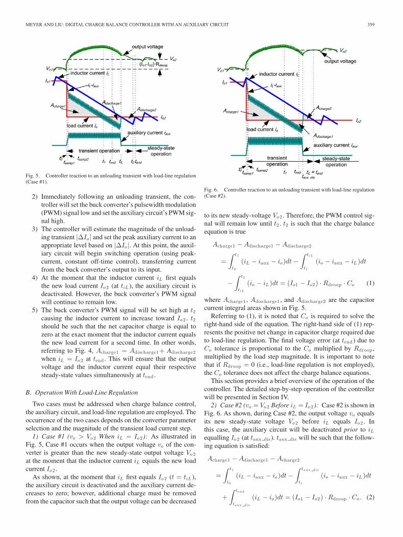
Fig. 5. Controller reaction to an unloading transient with load-line regulation(Case #1).
2) Immediately following an unloading transient, the con-troller will set the buck converter’s pulsewidth modulation(PWM) signal low and set the auxiliary circuit’s PWM sig-nal high.
3) The controller will estimate the magnitude of the unload-ing transient |ΔIo | and set the peak auxiliary current to anappropriate level based on |ΔIo |. At this point, the auxil-iary circuit will begin switching operation (using peak-current, constant off-time control), transferring currentfrom the buck converter’s output to its input.
4) At the moment that the inductor current iL first equalsthe new load current Io2 (at tiL ), the auxiliary circuit isdeactivated. However, the buck converter’s PWM signalwill continue to remain low.
5) The buck converter’s PWM signal will be set high at t2causing the inductor current to increase toward Io2 . t2should be such that the net capacitor charge is equal tozero at the exact moment that the inductor current equalsthe new load current for a second time. In other words,referring to Fig. 4, Acharge1 = Adischarge1+ Adischarge2when iL = Io2 at tend . This will ensure that the outputvoltage and the inductor current equal their respectivesteady-state values simultaneously at tend .
B. Operation With Load-Line Regulation
Two cases must be addressed when charge balance control,the auxiliary circuit, and load-line regulation are employed. Theoccurrence of the two cases depends on the converter parameterselection and the magnitude of the transient load current step.
1) Case #1 (vo > Vo2 When iL = Io2): As illustrated inFig. 5, Case #1 occurs when the output voltage vo of the con-verter is greater than the new steady-state output voltage Vo2at the moment that the inductor current iL equals the new loadcurrent Io2 .
As shown, at the moment that iL first equals Io2 (t = tiL ),the auxiliary circuit is deactivated and the auxiliary current de-creases to zero; however, additional charge must be removedfrom the capacitor such that the output voltage can be decreased
Fig. 6. Controller reaction to an unloading transient with load-line regulation(Case #2).
to its new steady-voltage Vo2 . Therefore, the PWM control sig-nal will remain low until t2 . t2 is such that the charge balanceequation is true
Acharge1 − Adischarge1 − Adischarge2
=∫ t1
t0
(iL − iaux − io)dt −∫ ti L
t1
(io − iaux − iL )dt
−∫ t2
ti L
(io − iL )dt = (Io1 − Io2) · Rdroop · Co (1)
where Acharge1 , Adischarge1 , and Adischarge2 are the capacitorcurrent integral areas shown in Fig. 5.
Referring to (1), it is noted that Co is required to solve theright-hand side of the equation. The right-hand side of (1) rep-resents the positive net change in capacitor charge required dueto load-line regulation. The final voltage error (at tend ) due toCo tolerance is proportional to the Co multiplied by Rdroop ,multiplied by the load step magnitude. It is important to notethat if Rdroop = 0 (i.e., load-line regulation is not employed),the Co tolerance does not affect the charge balance equations.
This section provides a brief overview of the operation of thecontroller. The detailed step-by-step operation of the controllerwill be presented in Section IV.
2) Case #2 (vo = Vo2 Before iL = Io2): Case #2 is shown inFig. 6. As shown, during Case #2, the output voltage vo equalsits new steady-state voltage Vo2 before iL equals Io2 . Inthis case, the auxiliary circuit will be deactivated prior to iLequalling Io2 (at taux dis). taux dis will be such that the follow-ing equation is satisfied:
Acharge1 − Adischarge1 − Acharge2
=∫ t1
t0
(iL − iaux − io)dt −∫ ta u x d i s
t1
(io − iaux − iL )dt
+∫ te n d
ta u x d i s
(iL − io)dt = (Io1 − Io2) · Rdroop · Co. (2)

360 IEEE TRANSACTIONS ON POWER ELECTRONICS, VOL. 28, NO. 1, JANUARY 2013
The buck converter’s PWM signal will be held low until theinductor current equals the new load current (at tiL ). At thispoint, the linear controller will retain control. The controller iscapable of automatically detecting the aforementioned cases.The detection method will be described in detail in Section IV.
III. MATHEMATICAL ANALYSIS OF CHARGE BALANCE
CONTROLLER WITH AUXILIARY CIRCUIT
This section will derive the charge balance equations nec-essary to implement digital charge balance control such that abuck converter, with the proposed auxiliary circuit, will recoverfrom an unloading transient with minimal settling time. Thecharge balance equations are presented at first without load-lineregulation and then with load-line regulation.
A. Without Load-Line Regulation
Referring to Fig. 4, it is noted that there is one positive integralarea of capacitor current Acharge1 and two negative integral areasof capacitor current Adischarge1 and Adischarge2 . The capacitorcharge area Acharge1 is derived as follows:
Acharge1 =∫∫ t1
t0
m2dtdt (3)
where m2 is the falling slew rate of the inductor current iL (m2 ≈Vo /Lo ) and t1 represents the first moment that the capacitorcurrent ic equals zero (i.e., when iL − Iaux avg = Io2).
It is noted that the inductor current slew rate is assumed inde-pendent of the output current. In other words, the dc resistance(DCR) of the inductor has been neglected. For low-voltage high-current applications, the inductor DCR is typically very low andcauses an insignificant effect on the inductor current slew rate.
Referring to Fig. 4, it is shown that the auxiliary circuit is de-activated when the inductor current equals the new load current(at tiL ). It is assumed that when the auxiliary circuit is deacti-vated, the auxiliary current iaux decreases to zero in negligibletime. This is a fair assumption since the falling iaux slew rate ismuch faster than the falling iL slew rate. For the charge balanceequations, the ripple of the auxiliary current is neglected sincethe high-frequency auxiliary switching causes the ripple’s effectto be neutralized.
With the aforementioned assumptions, Adischarge1 is calcu-lated as follows:
Adischarge1 =∫∫ ti L
t1
m2dtdt. (4)
Through geometric observation and simplification,Adischarge2 is expressed as follows:
Adischarge2 =∫∫ t2
ti L
m1 · m2 + m22
m1dtdt (5)
where m1 is the rising slew rate of the inductor current iL (m1 ≈(Vin − Vo )/Lo ). In order to ensure that vo and iL equal theirrespective steady-state values simultaneously, the net capacitor
Fig. 7. Digital double accumulator to determine t2 without load-lineregulation.
charge over the transient period must equal zero:
Acharge1 − Adischarge1 − Adischarge2 = 0∫∫ t1
t0
m2dtdt −∫∫ ti L
t1
m2dtdt −∫∫ t2
ti L
m1 · m2 + m22
m1dtdt
= 0. (6)
By dividing both sides of (6) by the constant m2 , substitutingthe known values for m1 and m2 , multiplying both sides by(Vin − Vo ), and simplifying, we obtain
(Vin − Vo) ·∫∫ t1
t0
dt dt − (Vin − Vo) ·∫∫ ti L
t1
dt dt
−Vin ·∫∫ t2
ti L
dt dt = 0. (7)
Therefore, by using (7), it is possible to determine the momentthat the buck converter’s PWM control signal should be set high(at t2), by the use of two accumulators, connected in series. Thewaveforms of the double accumulator are shown in Fig. 7.
The constant kacc represents the gain of the digital accumula-tors and is dependent on the system clock frequency. As shown,when the output of accumulator 2 returns to zero, t2 is deter-mined and the buck converter’s PWM signal is set high. Thiscontrol strategy is suitable when load-line regulation is not em-ployed; however, it must be modified when load-line regulationis employed.
B. With Load-Line Regulation
This section will be divided into Case #1 and Case #2, aspreviously described in Section II.
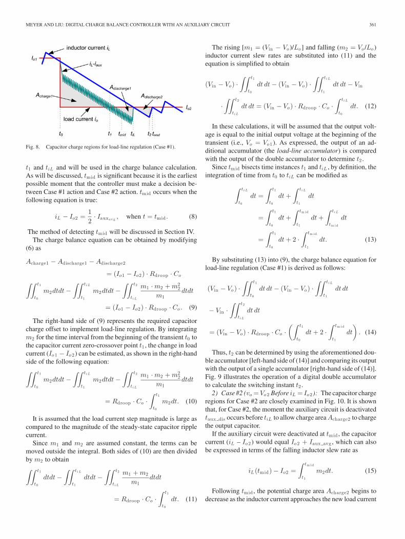
1) Case #1 (vo > Vo2 When iL = Io2): The capacitor chargeregions for Case #1 are illustrated in Fig. 8. As shown, a time in-stant tmid has been identified in Fig. 8. tmid bisects time instants
MEYER AND LIU: DIGITAL CHARGE BALANCE CONTROLLER WITH AN AUXILIARY CIRCUIT 361
Fig. 8. Capacitor charge regions for load-line regulation (Case #1).
t1 and tiL and will be used in the charge balance calculation.As will be discussed, tmid is significant because it is the earliestpossible moment that the controller must make a decision be-tween Case #1 action and Case #2 action. tmid occurs when thefollowing equation is true:
iL − Io2 =12· Iauxav g , when t = tmid . (8)
The method of detecting tmid will be discussed in Section IV.The charge balance equation can be obtained by modifying
(6) as
Acharge1 − Adischarge1 − Adischarge2
= (Io1 − Io2) · Rdroop · Co∫∫ t1
t0
m2dtdt −∫∫ ti L
t1
m2dtdt −∫∫ t2
ti L
m1 · m2 + m22
m1dtdt
= (Io1 − Io2) · Rdroop · Co. (9)
The right-hand side of (9) represents the required capacitorcharge offset to implement load-line regulation. By integratingm2 for the time interval from the beginning of the transient t0 tothe capacitor current zero-crossover point t1 , the change in loadcurrent (Io1 − Io2) can be estimated, as shown in the right-handside of the following equation:∫∫ t1
t0
m2dtdt −∫∫ ti L
t1
m2dtdt −∫∫ t2
ti L
m1 · m2 + m22
m1dtdt
= Rdroop · Co ·∫ t1
t0
m2dt. (10)
It is assumed that the load current step magnitude is large ascompared to the magnitude of the steady-state capacitor ripplecurrent.
Since m1 and m2 are assumed constant, the terms can bemoved outside the integral. Both sides of (10) are then dividedby m2 to obtain∫∫ t1
t0
dtdt −∫∫ ti L
t1
dtdt −∫∫ t2
ti L
m1 + m2
m1dtdt
= Rdroop · Co ·∫ t1
t0
dt. (11)
The rising [m1 = (Vin − Vo )/Lo ] and falling (m2 = Vo /Lo )inductor current slew rates are substituted into (11) and theequation is simplified to obtain
(Vin − Vo) ·∫∫ t1
t0
dt dt − (Vin − Vo) ·∫∫ ti L
t1
dt dt − Vin
·∫∫ t2
ti L
dt dt = (Vin − Vo) · Rdroop · Co ·∫ ti L
t0
dt. (12)
In these calculations, it will be assumed that the output volt-age is equal to the initial output voltage at the beginning of thetransient (i.e., Vo = Vo1). As expressed, the output of an ad-ditional accumulator (the load-line accumulator) is comparedwith the output of the double accumulator to determine t2 .
Since tmid bisects time instances t1 and tiL , by definition, theintegration of time from t0 to tiL can be modified as
∫ ti L
t0
dt =∫ t1
t0
dt +∫ ti L
t1
dt
=∫ t1
t0
dt +∫ tm id
t1
dt +∫ ti L
tm id
dt
=∫ t1
t0
dt + 2 ·∫ tm id
t1
dt. (13)
By substituting (13) into (9), the charge balance equation forload-line regulation (Case #1) is derived as follows:
(Vin − Vo) ·∫∫ t1
t0
dt dt − (Vin − Vo) ·∫∫ ti L
t1
dt dt
− Vin ·∫∫ t2
ti L
dt dt
= (Vin − Vo) · Rdroop · Co ·(∫ t1
t0
dt + 2 ·∫ tm id
t1
dt
). (14)
Thus, t2 can be determined by using the aforementioned dou-ble accumulator [left-hand side of (14)] and comparing its outputwith the output of a single accumulator [right-hand side of (14)].Fig. 9 illustrates the operation of a digital double accumulatorto calculate the switching instant t2 .
2) Case #2 (vo =Vo2 Before iL = Io 2): The capacitor chargeregions for Case #2 are closely examined in Fig. 10. It is shownthat, for Case #2, the moment the auxiliary circuit is deactivatedtaux dis occurs before tiL to allow charge area Acharge2 to chargethe output capacitor.
If the auxiliary circuit were deactivated at tmid , the capacitorcurrent (iL – Io2) would equal Io2 + Iaux avg , which can alsobe expressed in terms of the falling inductor slew rate as
iL (tmid) − Io2 =∫ tm id
t1
m2dt. (15)
Following tmid , the potential charge area Acharge2 begins todecrease as the inductor current approaches the new load current
362 IEEE TRANSACTIONS ON POWER ELECTRONICS, VOL. 28, NO. 1, JANUARY 2013
Fig. 9. Digital double accumulator to determine t2 with load-line regulation(Case #1).
Fig. 10. Capacitor charge areas for Case #2.
at a slew rate of m2 . Thus, Acharge2 is expressed as follows:
Acharge2 = Adischarge1
−∫ ta u x d i s
tm id
(iL (tmid) − Io2 − m2 ·
∫ ta u x d i s
tm id
dt
)dτ . (16)
By substituting (3), (4), (13), and (16) into (2), the chargebalance equation for Case #2 load-line regulation is expressedas follows:
∫∫ t1
t0
m2 dtdt −∫∫ ta u x d i s
t1
m2 dtdt +∫∫ tm id
t1
m2 dt dt
−∫ ta u x d i s
tm id
(∫ tm id
t1
m2dt −∫ ta u x d i s
midm2dt
)dτ
= Rdroop · Co
(∫ t1
t0
m2dt + 2 ·∫ tm id
t1
m2dt
). (17)
Fig. 11. Digital double accumulator to determine taux dis with load-lineregulation (Case #2).
By collecting like terms, (17) is simplified as∫∫ t1
t0
dtdt −∫ ta u x d i s
tm id
(2 ·
∫ tm id
t1
dt
)dt
= Rdroop · Co
(∫ t1
t0
dt + 2 ·∫ tm id
t1
dt
). (18)
By using (18), the output of a double accumulator (left-handside) can be compared to the output of a single accumulator(right-hand side) to determine the moment to deactivate theauxiliary circuit taux dis , as shown in Fig. 11.
In order to minimize the digital gate count of the controller, itis beneficial to design one double accumulator that can be usedfor Case #1, Case #2, and cases without load-line regulation. Inorder to achieve this, charge balance (18) can be modified bymultiplying both sides by (Vin − Vo ) as
(Vin −Vo) ·∫∫ t1
t0
dt dt− (Vin −Vo) ·∫ ta u x d i s
tm id
(2 ·
∫ tm id
t1
dt
)dτ
= Rdroop · Co · (Vin − Vo) ·(∫ t1
t0
dt + 2 ·∫ tm id
t1
dt
). (19)
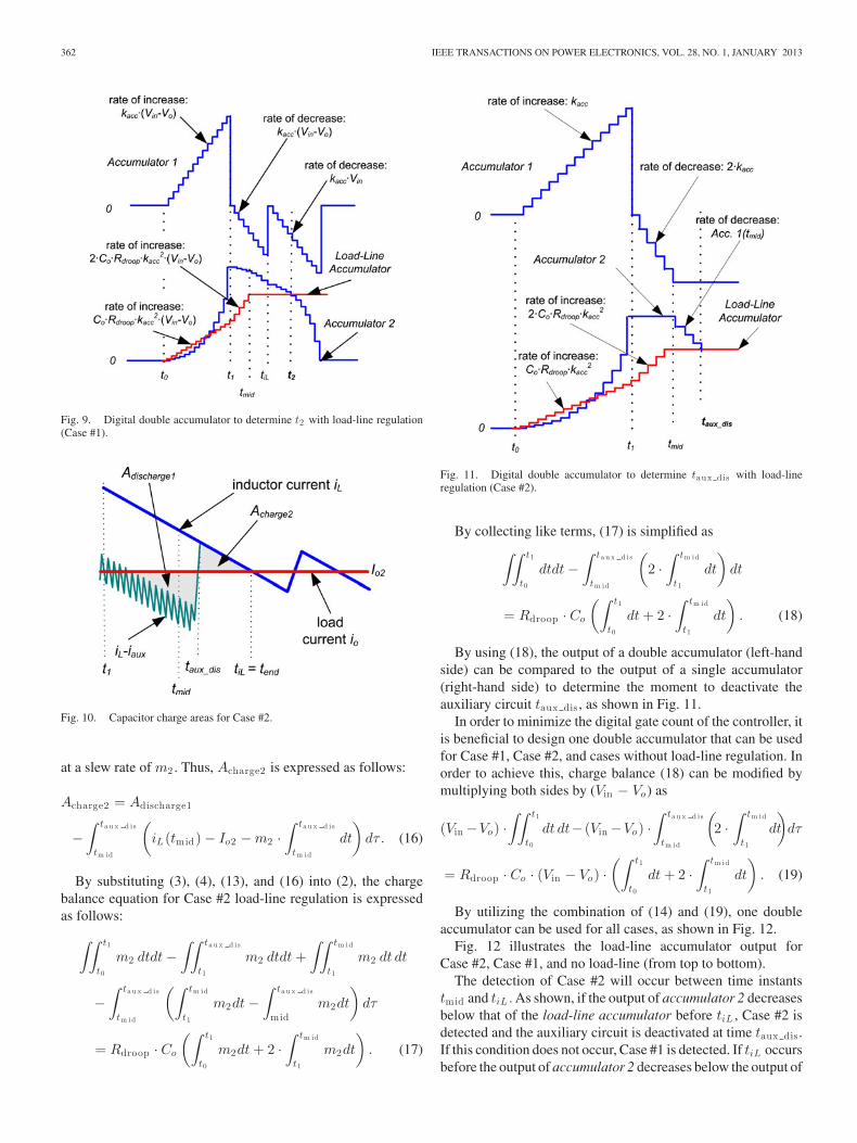
By utilizing the combination of (14) and (19), one doubleaccumulator can be used for all cases, as shown in Fig. 12.
Fig. 12 illustrates the load-line accumulator output forCase #2, Case #1, and no load-line (from top to bottom).
The detection of Case #2 will occur between time instantstmid and tiL . As shown, if the output of accumulator 2 decreasesbelow that of the load-line accumulator before tiL , Case #2 isdetected and the auxiliary circuit is deactivated at time taux dis .If this condition does not occur, Case #1 is detected. If tiL occursbefore the output of accumulator 2 decreases below the output of
MEYER AND LIU: DIGITAL CHARGE BALANCE CONTROLLER WITH AN AUXILIARY CIRCUIT 363
Fig. 12. Digital double accumulator operation for all possible cases.
the load-line accumulator, the auxiliary circuit is deactivated attiL , as shown in Figs. 4 and 5. In these cases, the buck converter’sPWM signal will remain low until output of accumulator 2decreases below the load-line accumulator’s output at time t2 .
Referring to the final charge balance equations (7), (14), and(19), it is noted that Lo has cancelled out of the equations. There-fore, the knowledge of Lo is not required for proper capacitorcharge balance. This is a significant advantage of the proposedcontrol method.
IV. DETAILED OPERATION AND IMPLEMENTATION OF CHARGE
BALANCE CONTROLLER WITH AUXILIARY CIRCUIT
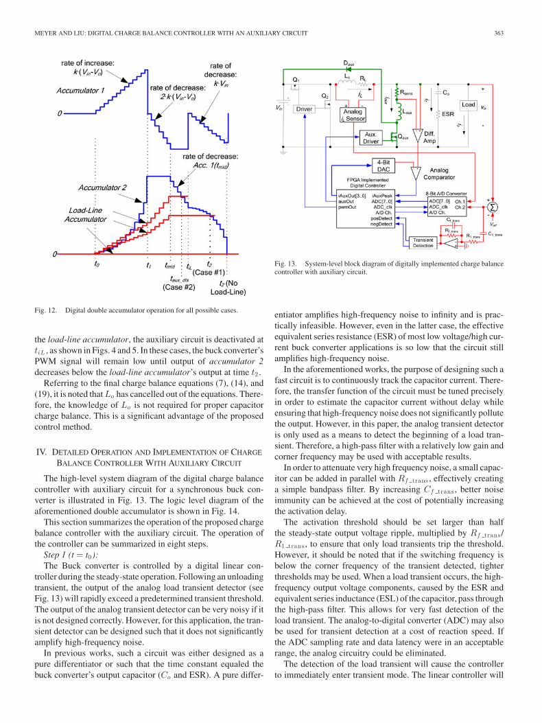
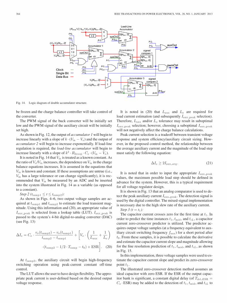
The high-level system diagram of the digital charge balancecontroller with auxiliary circuit for a synchronous buck con-verter is illustrated in Fig. 13. The logic level diagram of theaforementioned double accumulator is shown in Fig. 14.
This section summarizes the operation of the proposed chargebalance controller with the auxiliary circuit. The operation ofthe controller can be summarized in eight steps.
Step 1 (t = t0):The Buck converter is controlled by a digital linear con-
troller during the steady-state operation. Following an unloadingtransient, the output of the analog load transient detector (seeFig. 13) will rapidly exceed a predetermined transient threshold.The output of the analog transient detector can be very noisy if itis not designed correctly. However, for this application, the tran-sient detector can be designed such that it does not significantlyamplify high-frequency noise.
In previous works, such a circuit was either designed as apure differentiator or such that the time constant equaled thebuck converter’s output capacitor (Co and ESR). A pure differ-
Fig. 13. System-level block diagram of digitally implemented charge balancecontroller with auxiliary circuit.
entiator amplifies high-frequency noise to infinity and is prac-tically infeasible. However, even in the latter case, the effectiveequivalent series resistance (ESR) of most low voltage/high cur-rent buck converter applications is so low that the circuit stillamplifies high-frequency noise.
In the aforementioned works, the purpose of designing such afast circuit is to continuously track the capacitor current. There-fore, the transfer function of the circuit must be tuned preciselyin order to estimate the capacitor current without delay whileensuring that high-frequency noise does not significantly pollutethe output. However, in this paper, the analog transient detectoris only used as a means to detect the beginning of a load tran-sient. Therefore, a high-pass filter with a relatively low gain andcorner frequency may be used with acceptable results.
In order to attenuate very high frequency noise, a small capac-itor can be added in parallel with Rf trans , effectively creatinga simple bandpass filter. By increasing Cf trans , better noiseimmunity can be achieved at the cost of potentially increasingthe activation delay.
The activation threshold should be set larger than halfthe steady-state output voltage ripple, multiplied by Rf trans /R1 trans , to ensure that only load transients trip the threshold.However, it should be noted that if the switching frequency isbelow the corner frequency of the transient detected, tighterthresholds may be used. When a load transient occurs, the high-frequency output voltage components, caused by the ESR andequivalent series inductance (ESL) of the capacitor, pass throughthe high-pass filter. This allows for very fast detection of theload transient. The analog-to-digital converter (ADC) may alsobe used for transient detection at a cost of reaction speed. Ifthe ADC sampling rate and data latency were in an acceptablerange, the analog circuitry could be eliminated.
The detection of the load transient will cause the controllerto immediately enter transient mode. The linear controller will
364 IEEE TRANSACTIONS ON POWER ELECTRONICS, VOL. 28, NO. 1, JANUARY 2013
Fig. 14. Logic diagram of double accumulator structure.
be frozen and the charge balance controller will take control ofthe converter.
The PWM signal of the buck converter will be initially setlow and the PWM signal of the auxiliary circuit will be initiallyset high.
As shown in Fig. 12, the output of accumulator 1 will begin toincrease linearly with a slope of k · (Vin − Vo ) and the output ofaccumulator 2 will begin to increase exponentially. If load-lineregulation is required, the load-line accumulator will begin toincrease linearly with a slope of k2 ·Rdroop ·Co · (Vin − Vo ).
It is noted in Fig. 14 that Vin is treated as a known constant. Asthe ratio of Vo /Vin increases, the dependence on Vin in the chargebalance equations increases. It is assumed in the equations thatVin is known and constant. If these assumptions are untrue (i.e.,Vin has a large tolerance or can change significantly), it is rec-ommended that Vin be measured by an ADC and be insertedinto the system illustrated in Fig. 14 as a variable (as opposedto a constant).
Step 2 (tsamp1 ≤ t ≤ tsamp2):As shown in Figs. 4–6, two output voltage samples are ac-
quired at tsamp1 and tsamp2 to estimate the load transient mag-nitude. Using this information and (20), an appropriate value ofIaux peak is selected from a lookup table (LUT). Iaux peak ispassed to the system’s 4-bit digital-to-analog converter (DAC)(see Fig. 13)
ΔIo = Co ·vo(tsamp2) − vo(tsamp1)
tsamp2 − tsamp1+
[Vo ·
(1
Laux+
1Lo
)
·(tsamp2 − 1/2 · Tsamp − t0) + ESR]. (20)
At tsamp2 , the auxiliary circuit will begin high-frequencyswitching operation using peak-current constant off-timecontrol.
The LUT allows the user to have design flexibility. The appro-priate peak current is user-defined based on the desired outputvoltage response.
It is noted in (20) that Laux and Lo are required forload current estimation (and subsequently Iaux peak selection).Therefore, Laux and/or Lo tolerance may result in suboptimalIaux peak selection; however, choosing a suboptimal Iaux peakwill not negatively affect the charge balance calculations.
Peak current selection is a tradeoff between transient voltageresponse and system efficiency/auxiliary circuit sizing. How-ever, in the proposed control method, the relationship betweenthe average auxiliary current and the magnitude of the load stepmust satisfy the following equation:
ΔIo ≥ 2Iaux avg . (21)
It is noted that in order to input the appropriate Iaux peakvalues, the maximum possible load step should be defined inadvance for the system. However, this is a typical requirementfor all voltage regulator design.
It is shown in Fig. 13 that an analog comparator is used to de-tect the peak auxiliary current Iaux peak . The detection signal isused by the digital controller. The mixed-signal implementationis necessary due to the high slew rate of the auxiliary current.
Step 3 (t = t1):The capacitor current crosses zero for the first time at t1 . In
order to predict the time instances t1 , tmid , and tiL , a capacitorcurrent zero-crossover predictor is utilized. The predictor ac-quires output voltage samples (at a frequency equivalent to aux-iliary circuit switching frequency faux ) for a short period aftert0 . From these samples, it is possible to calculate the derivativeand estimate the capacitor current slope and magnitude allowingfor the fine resolution prediction of t1 , tmid , and tiL , as shownin Fig. 15.
In this implementation, three voltage samples were used to es-timate the capacitor current slope and predict its zero-crossoverpoint t1 .
The illustrated zero-crossover detection method assumes anideal capacitor with zero ESR. If the ESR of the output capac-itor bank is significant, a constant digital delay (of Tdel ESR =Co ·ESR) may be added to the detection of t1 , tmid , and tiL to

MEYER AND LIU: DIGITAL CHARGE BALANCE CONTROLLER WITH AN AUXILIARY CIRCUIT 365
Fig. 15. Prediction of t1 , tm id , and tiL by capacitor current zero-crossoverpredictor.
compensate. In the proposed controller, this was accomplishedby using a digital counter.
The detection of tmid and tiL is calculated based on the knowl-edge of the average auxiliary current Iaux avg . For each peakauxiliary current available through the aforementioned LUT, acorresponding Iaux avg must also be programmed into the con-troller. This allows the controller to accurately calculate tiL . Itshould be noted that there is no assumed relationship betweenIaux peak and Iaux avg . The controller allows for maximum flex-ibility. For example, if the value of Rsens were so large as to sig-nificantly alter the relationship between Iaux peak and Iaux avg ,this can easily be reflected in the programmed LUTs.
Referring to Fig. 12, at t1 , accumulator 1 is reset to zero.The input of accumulator 1 is set to −2(Vin − Vo ) and theenable input of accumulator 2 is set low. Thus, the output ofaccumulator 1 will begin to decrease at a rate of 2k(Vin − Vo )and the output of accumulator 2 will remain constant.
The channel select of the ADC is set to the inductor currentsensor at this point, and a sample of the inductor current is takenand passed to the linear controller. This will be used when load-line regulation is employed to allow for immediate load trackingby the linear controller when it regains control of the system.
Referring to Fig. 12, the input of the load-line accumulatoris switched to 2k ·Rdroop ·Co · (Vin − Vo ) at t1 .
Step 4 (t = tmid ):When the ic zero-crossover predictor indicates t = tmid , it
is known that iL − Io2 = 12 · Iaux avg . Referring to Fig. 12, at
t = tmid , the enable input of accumulator 1 is set low and theenable input of accumulator 2 is set high. Accumulator 2 is setto decrement mode, causing its output to decrease at a linear
rate equal to k ·Acc1(tmid ) (where Acc1(tmid ) equals the outputof accumulator 1 at t = tmid ).
As shown in Fig. 12, the enable input of the load-line accu-mulator is set low at tmid , causing its input to remain constantfollowing tmid .
Step 5 (t = taux dis) (Case #2 only):As shown in Fig. 12, if the output of accumulator 2 decreases
below that of the load-line accumulator before the inductorcurrent equals the new load current (at tiL ), then Case #2 isdetected. If this occurs, the auxiliary circuit is deactivated atthis moment (t = taux dis), as shown in Fig. 6. The PWM signalof the buck converter continues to be held low.
Step 6 (t = tiL ):When the inductor current equals the new load current for the
first time, t = tiL .If Case #2 was previously detected, this moment signifies the
end of the load transient and the linear controller retakes controlof the buck converter.
If Case #2 was not previously detected, accumulator 1 iscleared and its input is switched to −Vin . This causes accumu-lator 1’s output to decrease at a rate of k ·Vin and the output ofaccumulator 2 to decrease at an exponential rate. As shown inFigs. 4 and 5, the auxiliary circuit is deactivated and the PWMcontrol signal is held low following tiL .
Step 7 (t = t2) (No Load-Line Regulation or Case #1):When the output of accumulator 2 decreases below that of
the load-line accumulator (at t2), the PWM signal of the buckconverter is switched high and the inductor current begins toincrease toward the new load current, as shown in Figs. 4 and 5.
Step 8 (t = tend ):When the inductor current equals the new load current for the
first time (for Case #2) or the inductor current equals the newload current for a second time, it is determined that the transientis over. The second current crossover is detected using a digitalaccumulator (accumulator 3), as introduced in [2]. The linearcontroller is unfrozen and retakes control of the buck converter.If load-line regulation is used, the sampled inductor current (att1) is passed to the linear controller for instant load tracking.
V. SIMULATION RESULTS
The following simulation was conducted under the ideal case,without considering timing delays, digital quantization effects,etc.
All analog sampling/reaction delays were included in the sim-ulation; however, digital calculation delays were not included.The simulations were performed using a primarily analog-centric simulator that was not able to properly model the prop-agation delays of the field-programmable gate array (FPGA).However, since the system clock of the FPGA was 250 MHz,4-ns clock delays will have insignificant effects on the chargebalance time durations (which are typical three orders of mag-nitude larger).
The purpose of the simulation was to demonstrate the ef-fectiveness of the charge balance controller with the auxiliarycircuit over 1) a linear analog controller and 2) the charge bal-ance controller alone.

366 IEEE TRANSACTIONS ON POWER ELECTRONICS, VOL. 28, NO. 1, JANUARY 2013
Fig. 16. Simulated response to a 10 A→0 A load current step change withoutload-line regulation (Iaux avg = 3.8 A).
The parameters of the simulated buck converter were as fol-lows: Vin = 12 V, Vo = 1.5 V, fsw = 400 kHz, Lo = 1 μH,Lo DCR = 1 mΩ, Co = 180 μF, ESR = 0.5 mΩ, and ESL =100 pH. The auxiliary circuit parameters were Laux = 100 nH,Laux DCR = 0.3 mΩ), and faux ≈ 2 MHz.
Fig. 16 shows the simulated comparison (without load-lineregulation) of a voltage-mode controlled converter, a charge bal-ance controlled converter (without auxiliary circuit [2]), a con-verter with the auxiliary circuit (without charge balance con-trol [12]), and the proposed digital charge balance controllerwith auxiliary circuit undergoing a 10 A→0 A load step. In thiscase, the auxiliary circuit sets Iaux avg to approximately 3.8 A.
It is illustrated that the voltage deviation magnitude and thesettling time is improved significantly over previously proposedsolutions. The buck converter with the proposed controller andauxiliary circuit has an output voltage overshoot of 65 mV anda settling time of 9 μs.
The transient response was also simulated with load-line reg-ulation. The output impedance Rdroop was set to 5 mΩ. Fig. 17illustrates a simulated comparison between a voltage-mode con-trolled converter, a digital charge balance controlled buck con-verter (without auxiliary circuit) [2], and the proposed digitalcharge balance controller with auxiliary circuit. Each converterundergoes a 10 A→0 A load step transient. The peak auxil-iary current is set such that the average auxiliary current equalsIaux avg = 3.8 A.
It is illustrated that the voltage deviation magnitude and thesettling time are improved significantly over previously pro-posed solutions. The buck converter with the proposed controllerand auxiliary circuit has an output voltage overshoot of 18 mV(68–50 mV) over the new steady-state voltage (68 mV over theoriginal steady-state voltage) and a settling time of 7 μs.
VI. EXPERIMENTAL RESULTS
The proposed controller was implemented on an AlteraCyclone II FPGA. The chip is capable of utilizing over 70 000
Fig. 17. Simulated response to a 10 A→0 A load current step change withload-line regulation (Iaux avg = 3.8 A).
logic elements; however, the charge balance controller (includ-ing the ic zero-crossover predictor and the double accumulatorblocks) only requires a total of approximately 450 logic ele-ments. As a reference point, the digital-type III compensatorand digital pulsewidth modulator require 450 logic elements toimplement (not including its LUTs). It is important to note thatmultiplier, divider, square root, or 2-D LUTs are not required toimplement the digital charge balance controller.
As noted in Fig. 15, the effective sampling frequency shouldequal the auxiliary switching frequency in order to predict thecapacitor current zero-crossover point. If the chosen ADC has amulticycle latency, it may be necessary to use a faster ADC andoversample in order to reduce data latency. The effective datalatency must be compensated for in the capacitor zero-crossoveralgorithm. In the experimental prototype, the ADC latency was40 ns.
The high-pass filter corner frequency of the analog transientdetector was set to approximately 600 kHz, and the gain was setto 5. Therefore, the parameters were C1 trans = 1 nF, R1 trans =300 Ω, and Rf trans = 1.5 kΩ. Cf trans was equal to 10 pF. Thebuck converter and auxiliary circuit parameters were identicalto those of the simulation.
Fig. 18 illustrates the controller’s reaction to an 11.5 A→0 Aload step (without load-line regulation). For this unloading mag-nitude, the auxiliary current was set to approximately Iaux avg =3.5 A.
It should be noted that the simulation test conditions (loadstep magnitude and auxiliary current) are slightly different thanthe experimental prototype test conditions; therefore, the resultsdiffer as well. As mentioned, the primary purpose of the simula-tion was to compare to previous works in order to demonstratethe effective improvement. Thus, the simulation results werechosen to match the conditions of the previous work. For refer-ence, the time instants t0–tend were superimposed on the scopedisplay to better illustrate the controller’s behavior.
The converter is capable of recovering from the load transientwithin 9 μs with a voltage overshoot of 70 mV.

MEYER AND LIU: DIGITAL CHARGE BALANCE CONTROLLER WITH AN AUXILIARY CIRCUIT 367
Fig. 18. Digital charge balance controller’s response to a 11.5 A→0 A loadstep without load-line regulation.
Fig. 19. Digital charge balance controller’s response (without auxiliary cir-cuit) to a 11.5 A→0 A load step without load-line regulation.
Fig. 19 illustrates the unloading transient response of thedigital charge balance controller (introduced in [2]) without theuse of the auxiliary circuit.
As observed, the use of the auxiliary circuit improves thesettling time by 25% (12 μs→9 μs) and improves the voltageovershoot by 56% (160 mV→70 mV) over that of the digitalcharge balance controller alone.
Therefore, if the auxiliary circuit were not utilized anda 70 mV overshoot was still required, the output capaci-tance would need to be increased to approximately 180 μF ×(160 mV/70 mV) = 411 μF (neglecting ESR effects).
Therefore, assuming the output capacitance was made upof ten 0805 size 22-μF ceramic capacitors (with an effective
Fig. 20. Digital charge balance controller’s response to a 11.5 A→0 A loadstep without load-line regulation (inductor current and auxiliary current).
capacitance of 18 μF due to dc bias), an additional 13 capacitorswould be required to reduce the overshoot to 70 mV. Thus, anadditional area of (13 × 2 mm × 1.3 mm plus an x-directioncomponent to component spacing of 0.4 mm) 42.6 mm2 wouldbe required.
To estimate the optimized area of the auxiliary circuitry, thefollowing assumptions are made: 1) the additional auxiliaryMOSFET driver can and control circuitry can be integrated inthe existing controller, 2) Q_aux and D_aux could be integratedtogether in a 3 mm × 3 mm QFN package (similar to Infineon’sBSZ0907ND), 3) the inductor footprint space is 5.18 mm ×5.49 mm (similar to Vishay Dale’s IHLP-2020BZ-01), and 4) a1206 (3.2 mm× 1.6 mm) resistor could be used for current sens-ing. Based on these assumptions, the auxiliary circuitry wouldbe approximately 42.5 mm2 . Fig. 20 illustrates the inductorcurrent (measured from the analog inductor current filter) andthe auxiliary current. For reference, the load current and timeinstants t0–tend were superimposed on the graph.
As shown in Fig. 20, the auxiliary circuit is deactivated whenthe inductor current first equals the new load current (at tiL ).However, the buck converter’s PWM signal is kept low until t2is determined. This is to allow additional charge to be removedfrom the output capacitor such that the output voltage equals thereference voltage at the exact moment that the inductor currentequals its new steady-state value.
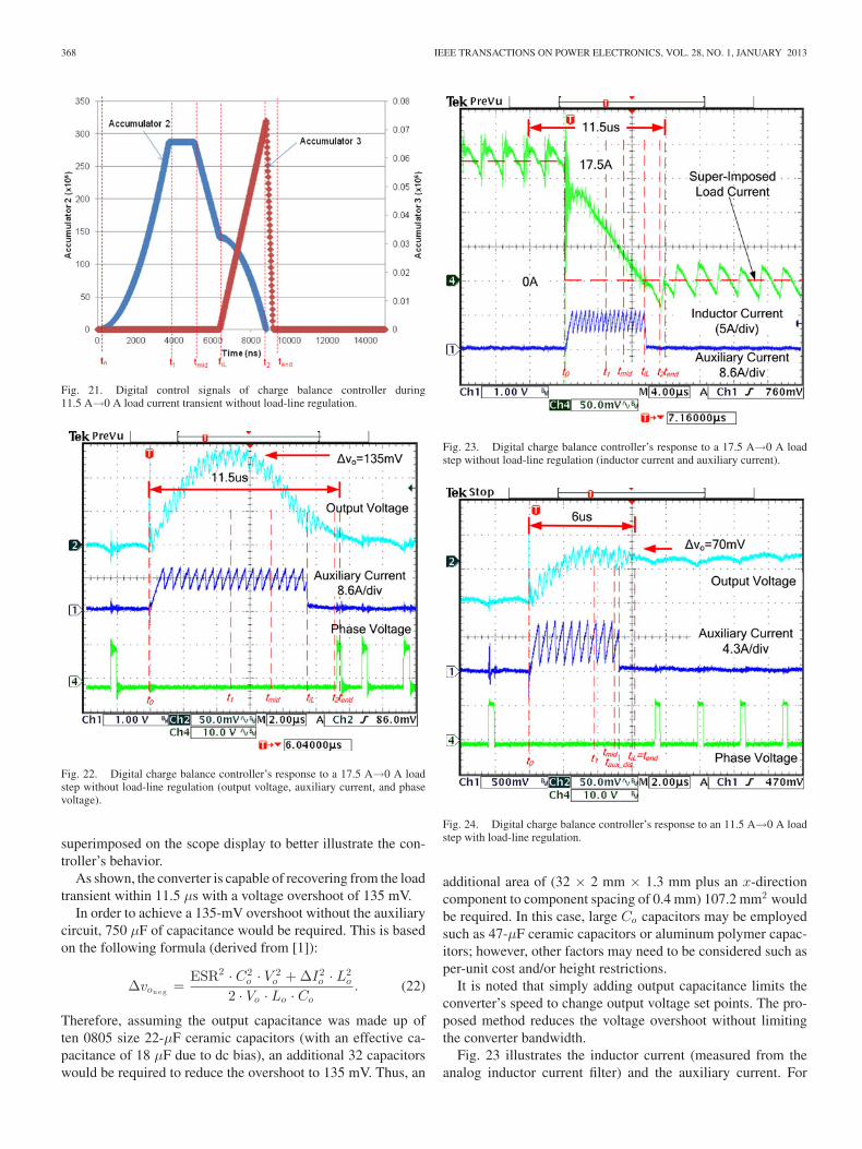
Fig. 21 illustrates the digital signals of the controller duringthe unloading transient. The digital signals were extracted dur-ing experimental tests using an embedded logic analyser. For ref-erence, time instants t0–tend were superimposed on the graph.Fig. 22 illustrates the controller’s reaction to a 17.5 A→0 Aload step (without load-line regulation). For this unloading tran-sient magnitude, the auxiliary current was set to approximatelyIaux avg = 8 A. For reference, the time instants t0–tend were
368 IEEE TRANSACTIONS ON POWER ELECTRONICS, VOL. 28, NO. 1, JANUARY 2013
Fig. 21. Digital control signals of charge balance controller during11.5 A→0 A load current transient without load-line regulation.
Fig. 22. Digital charge balance controller’s response to a 17.5 A→0 A loadstep without load-line regulation (output voltage, auxiliary current, and phasevoltage).
superimposed on the scope display to better illustrate the con-troller’s behavior.
As shown, the converter is capable of recovering from the loadtransient within 11.5 μs with a voltage overshoot of 135 mV.
In order to achieve a 135-mV overshoot without the auxiliarycircuit, 750 μF of capacitance would be required. This is basedon the following formula (derived from [1]):
Δvon e g =ESR2 · C2
o · V 2o + ΔI2
o · L2o
2 · Vo · Lo · Co. (22)
Therefore, assuming the output capacitance was made up often 0805 size 22-μF ceramic capacitors (with an effective ca-pacitance of 18 μF due to dc bias), an additional 32 capacitorswould be required to reduce the overshoot to 135 mV. Thus, an
Fig. 23. Digital charge balance controller’s response to a 17.5 A→0 A loadstep without load-line regulation (inductor current and auxiliary current).
Fig. 24. Digital charge balance controller’s response to an 11.5 A→0 A loadstep with load-line regulation.
additional area of (32 × 2 mm × 1.3 mm plus an x-directioncomponent to component spacing of 0.4 mm) 107.2 mm2 wouldbe required. In this case, large Co capacitors may be employedsuch as 47-μF ceramic capacitors or aluminum polymer capac-itors; however, other factors may need to be considered such asper-unit cost and/or height restrictions.
It is noted that simply adding output capacitance limits theconverter’s speed to change output voltage set points. The pro-posed method reduces the voltage overshoot without limitingthe converter bandwidth.
Fig. 23 illustrates the inductor current (measured from theanalog inductor current filter) and the auxiliary current. For

MEYER AND LIU: DIGITAL CHARGE BALANCE CONTROLLER WITH AN AUXILIARY CIRCUIT 369
Fig. 25. Digital charge balance controller’s response to an 11.5 A→0 A loadstep with load-line regulation (inductor current and auxiliary current).
Fig. 26. Digital control signals of charge balance controller during11.5 A→0 A load current transient with load-line regulation (Case #2).
reference, the load current and time instants t0–tend were super-imposed on the graph. As shown in Figs. 22 and 23, the inductorcurrent returns to the new load current at moment that the out-put voltage returns to its reference value. Fig. 24 illustrates thecontroller’s reaction to an 11.5 A→0 A load step (with load-lineregulation). Fig. 25 illustrates the inductor current (measuredfrom the analog inductor current sensor). Fig. 26 shows the ex-perimentally obtained digital signals of the controller during thenegative load current step transient with load-line regulation.
Since the output of accumulator 2 is less than that of theload-line accumulator before tiL , Case #2 is detected and theauxiliary current is deactivated at taux dis to allow the capacitorcharge areas to balance by time tiL . This results in a smoothtransition as the output voltage equals its new steady-state valueat the exact moment that the inductor current equals the newload current. The converter is able to recover from the unloading
step within 6 μs and with only a 10 mV (70–60 mV) overshootbeyond the final steady-state voltage.
VII. CONCLUSION
In this paper, a novel digital charge balance control methodis described capable of reducing the voltage overshoot of abuck converter (through the use of an auxiliary circuit) and im-plementing load-line regulation. The proposed digital controllerdoes not require multipliers, dividers, or 2-D LUTs, significantlyreducing the IC real-estate required. The proposed control algo-rithm consumes an additional 450 Altera logic elements over the450 logic elements required for the steady-state voltage-modecontroller.
The use of the auxiliary circuit significantly reduces the volt-age overshoot (due to an unloading transient) beyond the phys-ical capabilities of the buck converter alone. It is shown thatby implementing the charge balance principle with the auxil-iary circuit, the settling time can be also significantly improvedover previously proposed solutions. In addition, it is demon-strated that load-line regulation can be implemented while stillallowing for a nearly seamless transition between the nonlin-ear and linear control methods. Extensive experimental resultsare provided to verify the advantages of the proposed controlmethod.
REFERENCES
[1] E. Meyer, Z. Zhang, and Y.-F. Liu, “An optimal control method for buckconverters using a practical capacitor charge balance technique,” IEEETrans. Power Electron., vol. 23, no. 4, pp. 1802–1812, Jul. 2008.
[2] E. Meyer, Z. Zhang, and Y. F. Liu, “Digital charge balance controllerwith low gate count to improve the transient response of buck converters,”in Proc. IEEE Energy Convers. Congr. Expo., San Jose, CA, Sep. 2009,pp. 3320–3327.
[3] K. K. S. Leung and H. S. H. Chung, “A comparative study of boundarycontrol with first- and second-order switching surfaces for buck convertersoperating in DCM,” IEEE Trans. Power Electron., vol. 22, no. 4, pp. 1196–1209, Jul. 2007.
[4] T. Geyer, G. Papafotiou, R. Frasca, and M. Morari, “Constrained optimalcontrol of step-down DC–DC converter,” IEEE Trans. Power Electron.,vol. 23, no. 5, pp. 2454–2464, Sep. 2008.
[5] M. Oronez, M. T. Iqbal, and J. E. Quaicoe, “Selection of a curved switchingsurface for buck converters,” IEEE Trans. Power Electron., vol. 21, no. 4,pp. 1148–1153, Jul. 2006.
[6] A. Soto, A. de Castro, P. Alou, J. A. Cobos, J. Uceda, and A. Lotfi,“Analysis of the buck converter for scaling the supply voltage of digitalcircuits,” IEEE Trans. Power Electron., vol. 22, no. 4, pp. 1196–1209,Jul. 2007.
[7] G. Feng, E. Meyer, and Y. F. Liu, “A new digital control algorithm toachieve optimal dynamic response performance in DC-to-DC convert-ers,” IEEE Trans. Power Electron., vol. 22, no. 4, pp. 1489–1498, Jul.2007.
[8] Z. Zhao and A. Prodic, “Continuous-time digital controller for high-frequency DC–DC converters,” IEEE Trans. Power Electron., vol. 23,no. 2, pp. 564–573, Mar. 2008.
[9] S. Effler, A. Kelly, M. Halton, T. Kruger, and K. Rinne, “Digital controllaw using a novel load current estimator principle for improved transientresponse,” in Proc. IEEE Power Electron. Spec. Conf., 2008, pp. 4585–4589.
[10] L. Corradini, A. Costabeber, P. Mattavelli, and S. Saggini, “Parameter-independent time-optimal digital control for point-of-load converters,”IEEE Trans. Power Electron., vol. 24, no. 10, pp. 2235–2248, Oct. 2009.
[11] V. Yousefzedah, A. Babazadeh, B. Ramachandran, E. Alarcon, L. Pao,and D. Maksimovic, “Proximate time-optimal control for synchronousbuck DC–DC converters,” IEEE Trans. Power Electron., vol. 23, no. 4,pp. 2018–2026, Jul. 2008.
370 IEEE TRANSACTIONS ON POWER ELECTRONICS, VOL. 28, NO. 1, JANUARY 2013
[12] E. Meyer, Z. Zhang, and Y. F. Liu, “Controlled auxiliary circuit to improveunloading transient response of buck converters,” IEEE Trans. PowerElectron., vol. 25, no. 4, pp. 806–819, Apr. 2010.
[13] R. Singh and A. Khambadkone, “A buck derived topology with improvedstep-down transient performance,” IEEE Trans. Power Electron., vol. 23,no. 6, pp. 2855–2866, Nov. 2008.
[14] M. Rico, J. Uceda, J. Sebastian, and F. Aldana, “Static and dynamicmodeling of tapped-inductor DC-to-DC converters,” in Proc. IEEE PowerElectron. Spec. Conf., 1987, pp. 281–288.
[15] D. D.-C. Lu, J. C. P. Liu, F. N. K. Poon, and B. M. H. Pong, “A singlephase voltage regulator module (VRM) with stepping inductance for fasttransient response,” IEEE Trans. Power Electron., vol. 22, no. 2, pp. 417–424, Mar. 2007.
[16] A. Stupar, Z. Lukic, and A. Prodic, “Digitally-controlled steered-inductorbuck converter for improving heavy-to-light load transient response,” inProc. IEEE Power Electron. Spec. Conf., Jun. 2008, pp. 3950–3954.
[17] X. Wang, I. Batarseh, S. A. Chickamennahalli, and E. Standford, “VRtransient improvement at high slew rate load—Active transient voltagecompensator,” IEEE Trans. Power Electron., vol. 22, no. 4, pp. 1472–1479, Jul. 2007.
[18] H. Zhou, X. Wang, T. Wu, and I. Batarseh, “Magnetics design for ac-tive transient voltage compensator,” in Proc. IEEE Appl. Power Electron.Conf., 2006, pp. 567–572.
[19] O. Abdel-Rahman and I. Batarseh, “Transient response improvement inDC–DC converters using output capacitor current for faster transient de-tection,” in Proc. IEEE Power Electron. Spec. Conf., Jun. 2007, pp. 157–160.
[20] X. Wang, L. Qingshui, and I. Batarseh, “Transient response improvementin isolated DC–DC converter with current injection circuit,” in Proc. IEEEAppl. Power Electron. Conf., Mar. 2005, pp. 706–710.
[21] A. Barrado, A. Lazaro, R. Vazquez, V. Salas, and E. Olias, “The fastresponse double buck DC–DC converter (FRDB): Operation and outputfilter influence,” IEEE Trans. Power Electron., vol. 20, no. 6, pp. 1261–1270, Nov. 2005.
[22] A. M. Wu and S. R. Sanders, “An active clamp circuit for voltage regulationmodule (VRM) applications,” IEEE Trans. Power Electron., vol. 16, no. 5,pp. 623–634, Sep. 2001.
[23] Y. Wen and O. Trescases, “DC–DC converter with digital adaptive slopecontrol in auxiliary phase for optimal transient response,” in Proc. IEEEAppl. Power Electron. Conf., Mar. 2011, pp. 331–337.
Eric Meyer (S’05–M’10) received the B.Sc.and Ph.D. degrees in electrical and com-puter engineering from Queen’s University,Kingston, ON, Canada, in 2005 and 2010,respectively.
He is currently a Power Electronics DesignEngineer with Advanced Micro Devices, Markham,ON. He has authored or coauthored more than 21technical papers in conferences or IEEE Journals andhas one patent pending. During his graduate studies,he was awarded several scholarships including the
National Sciences and Engineering Research Council scholarship from thegovernment of Canada. His current research interests include novel topologiesand control methods to improve the dynamic response of voltage regulators.
Yan-Fei Liu (M’94–SM’97) received the B.Sc. andM.Sc. degrees in electrical engineering from Zhe-jiang University, Hangzhou, China, in 1984 and1987, respectively, and the Ph.D. degree in electricaland computer engineering from Queen’s University,Kingston, ON, Canada, in 1994.
He is currently a Professor in the Department ofElectrical and Computer Engineering, Queen’s Uni-versity. From February 1994 to July 1999, he was aTechnical Advisor with the Advanced Power SystemDivision, Astec (formerly Nortel Networks), where
he was involved in high-quality design, new products, and technology devel-opment. His current research interests include digital control technologies fordc–dc switching converter and ac–dc converter with power factor correction,current-source MOSFET drive technology, topologies and control for voltageregulator application, electromagnetic interference filter design methodologiesfor switching converters, topologies and controls for high-switching frequency,low-switching loss converters, modeling and analysis of core loss and copperloss for high-frequency planar magnetics, and large signal modeling of switch-ing converters.
Dr. Liu is the recipient of the Premiere’s Research Excellent Award in 2001,the Golden Apple Teaching Award in 2000, 2008, and 2009, all in Queen’s Uni-versity, and the 1997 Award in Excellence in Technology in Nortel Networks.