ieee xplore full-text html
DESCRIPTION
paper n temp sensorsTRANSCRIPT
9/16/2015 IEEE Xplore FullText HTML :
http://ieeexplore.ieee.org/xpls/icp.jsp?arnumber=4449483 1/13
Sign Out
Access provided by:Jaypee Insituite of InformationTechnologyNoida Sec 128 (L3)
IEEE.org IEEE Xplore Digital Library| IEEESA| IEEE Spectrum| More Sites| Cart (0) Create Account| Personal Sign In|
Abstract Authors Figures Multimedia References Cited By Keywords
Integrated temperature sensor with digital output forSoC power managementIn this paper a novel compact CMOS temperature sensor with builtin analogue to digitalconversion and calibration is presented. It has been implemented in ST's 90 nm and 65nm processes and is part of ST's lowpower platform strategy to optimize SoC powerconsumption and performance.
This paper appears in: Design & Technology of Integrated Systems in Nanoscale Era, 2007. DTIS.International Conference on , Issue Date: 25 Sept. 2007 , Written by: Vogt, Lionel; Chara, Youness;Ouannani, Hicham; Nazih, Maria
©2007 IEEE
BROWSE MY SETTINGS GET HELP WHAT CAN I ACCESS?
SECTION I.INTRODUCTION
In the Nanometerera, SystemonChip power dissipation has increased dramatically with the ability to integrate more processing power. The temperaturedependant behavior of digital circuits has also become more complex to manage with the sharp increase of leakage currents and the apparition oftemperature inversion.
Therefore, monitoring the internal junction temperature is mandatory, firstly to maintain circuits within safe operating range, secondly to optimize theirperformance.
Managing the dynamic power consumption, leakage and operating speed of a complex SoC by adapting the activity, frequency and supply according tocertain indicators, such as internal junction temperature has been presented in [1].
Important temperature gradients can also be observed across a SoC depending of the activity of its subsystems, giving rise to the need for low area sensorswhich can be distributed conveniently.
Integrated CMOS temperature sensors have therefore emerged as a crucial enabling IP for systemlevel low power and performance optimization.
We present an original temperature sensor offering the following features: compact architecture and circuit area, robustness for integration in a digitalenvironment, embedded analoguetodigital conversion and calibration.
SECTION II.PRINCIPLES OF TEMPERATURESENSORS
Many implementations of temperature sensors have been reported, relying on the wellknown temperature dependency of bipolar devices, available assubstrate PNPs in a CMOS process.

9/16/2015 IEEE Xplore FullText HTML :
http://ieeexplore.ieee.org/xpls/icp.jsp?arnumber=4449483 2/13
II.1. Proportional to Absolute Temperature (PTAT) source
Figure 1: PTAT voltage source.
A good approximation of the bipolar transistor collector current in the mediumlevel injection is:
View Source
But for PNP bipolar in CMOS technology, only the emitter current is accessible.
As Ie is related to Ic by forward current gain , we can write
View Source
For large values of can be approximated by , and the difference of the baseemitter voltages Vptat(T) becomes
View Source
where is Boltzmann's constant, is the electron charge, is the ratio of the bias currents of Ql and Q2 and is the ratio of their emitter areas [3].
The PTAT voltage temperature coefficient in equation (3) is independent from process parameters.
For CMOS substrate PNPs however, the gain is low and varies with current density and temperature.
can be rewritten as:
= ( − 1) ≈Ic Is eqVBE
KT IseqVBE
KT (1)
β
= (1 + ) = (1 + )Ie Ic1β
1β
IseqVBE
KT (2)
β, Ie Ic
(T ) = ln (m. n) = TVPTAT
kT
qλPTAT (3)
k q m n
β
λPTAT
= (ln(m. n) + ln ( ))λPTAT
k
q
1 + 1/β2
1 + 1/β1(4)

9/16/2015 IEEE Xplore FullText HTML :
http://ieeexplore.ieee.org/xpls/icp.jsp?arnumber=4449483 3/13
View Source
This will cause a process and temperature dependent error, this sensitivity to can be reduced by increasing m.n.
II2 VBE & Bandgap Voltage generation
Bandgap voltage references are based on the addition of two voltage sources with opposite temperature coefficient. The VBE of bipolar devices biased by aPTAT current [3] is:
View Source
VBE is essentially a voltage with a temperature coefficient around −2mV/K and a temperature dependant curvature term described by c(T).
One may obtain a temperature independent voltage source, by summing the VBE voltage and a PTAT source in order to cancel out their temperaturecoefficients around a center value, by choosing appropriately in (6).
View Source
The curvature term remains, techniques exist to correct it but it will not be necessary in our application.
Such a reference is related to the silicon bandgap voltage, hence is an absolute reference with good accuracy.
II2 Temperature Sensors with accurate A/D conversion
Since it is possible to generate PTAT voltage and absolute reference with proven techniques, it is natural to convert temperature to a digital value by feedinga PTAT input to an ADC referenced to a bandgap voltage [2].
Unfortunately, since VPTAT exhibits a slope in the order of 0.2mV/K, a high precision amplification is required prior to A/D conversion, employingsophisticated noise and offset reduction techniques such as switchedcapacitor integrating chopper amplifier, which are of utmost elegance but costly.
An alternative architecture has been proposed in [3] and [4], smartly avoiding to amplify be and Vref separately, but integrating the difference in asigmadelta loop which nulls its average, shown in the following diagram.
Figure 2: Simplified sensor presented in [3] and [4]
Solving for the average value of the bitstream × yields
View Source
Appropriate values for and make D temperature independent, thus x is a linear representation of temperature. The optimum is actually to give D apositive TC to eliminate curvature error in the digital output [4]
β
(T ) = − T − c(T )VBE VBE0 λPTAT (5)
α
(T ) = + αVREF VBE0 VPTAT (6)
ΔV
x = =β × ΔV be
α × V be + β × ΔV be
N
D(7)
α β
9/16/2015 IEEE Xplore FullText HTML :
http://ieeexplore.ieee.org/xpls/icp.jsp?arnumber=4449483 4/13
Unfortunately, first order SigmaDelta modulators processing DC signals suffer from limitations such as limit cycles, which lead the authors to employ asecondorder loop with a reset system and complex digital filtering. Although extremely accurate this architecture is too area and power consuming for us.
A continuoustime sigmadelta ADC also offers little flexibility with regards to clock frequency.
However, the key advantage is to process the difference of PTAT and VBE source, actually in the form of currents.
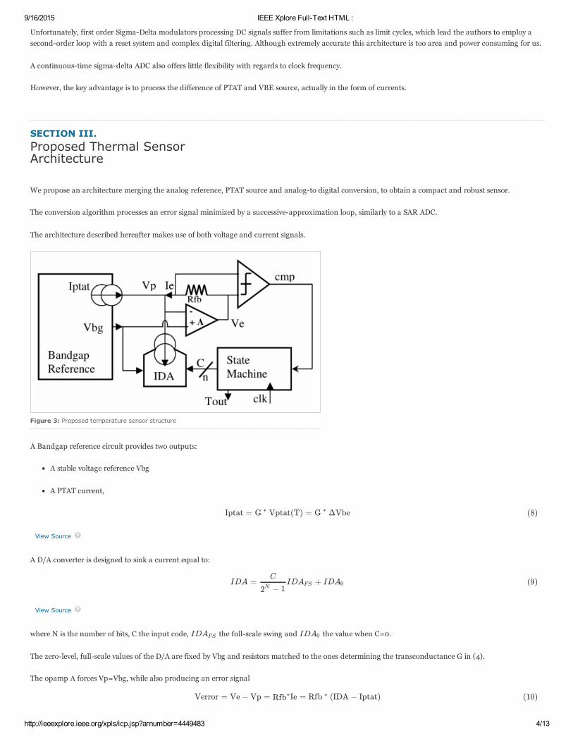
SECTION III.Proposed Thermal SensorArchitecture
We propose an architecture merging the analog reference, PTAT source and analogto digital conversion, to obtain a compact and robust sensor.
The conversion algorithm processes an error signal minimized by a successiveapproximation loop, similarly to a SAR ADC.
The architecture described hereafter makes use of both voltage and current signals.
Figure 3: Proposed temperature sensor structure
A Bandgap reference circuit provides two outputs:
A stable voltage reference Vbg
A PTAT current,
View Source
A D/A converter is designed to sink a current equal to:
View Source
where N is the number of bits, C the input code, the fullscale swing and the value when C=0.
The zerolevel, fullscale values of the D/A are fixed by Vbg and resistors matched to the ones determining the transconductance G in (4).
The opamp A forces Vp=Vbg, while also producing an error signal
Iptat = G Vptat(T) = G ΔVbe ∗ ∗ (8)
IDA = ID + IDC
− 12NAFS A0 (9)
IDAFS IDA0
Verror = Ve − Vp = Ie = Rfb (IDA − Iptat)Rfb∗ ∗ (10)

9/16/2015 IEEE Xplore FullText HTML :
http://ieeexplore.ieee.org/xpls/icp.jsp?arnumber=4449483 5/13
View Source
The comparator senses the sign of Ve and sends a logic output cmp to the state machine
The latter, with a simple iterative algorithm, adjusts the digital code C to obtain Ve as close to zero as possible, which translates into the followingcondition:
View Source
From the above equation we can derive:
View Source
Since is proportional to absolute temperature and both and are derived from a temperature independent reference, C is a lineardigital representation of temperature. We can simply derive how to choose the above values according to the desired temperature range.
Let us note and the minimum and maximum temperatures of operation respectively, corresponding to the codes C=0 and
Let us note:
With (11) we find how to fix the D/A range:
View Source
and
View Source
Substitution in (12) shows that
View Source
A trivial example is to chose , C is then the integer value of T Celcius.
G ∗ ΔVbe − IDA = 0. (11)
C = ( − 1) ×2N G × ΔV be − IDA0
IDAFS
(12)
ΔV be IDA0 IDAFS
T0 T1 C = ( − 1)2N
G × ΔV be = B × T
ID = B ×A0 T0 (13)
ID = B × ( − )AFS T1 T0 (14)
C = ( − 1)2N (T − )T0
( − )T1 T0(15)
= 273 K = C, = 400 K = C, N = 7T0 0∘ T1 127∘
SECTION IV.Circuit implementation
The above architecture can be implemented simply:

9/16/2015 IEEE Xplore FullText HTML :
http://ieeexplore.ieee.org/xpls/icp.jsp?arnumber=4449483 6/13
Figure 4: Circuitlevel implementation
The building blocks corresponding to Figure 3 are highlighted by the dotted boxes.
The Bandgap reference produces a voltage output (nominally 1.21V) and a PTAT current.
The D/A converter can be implemented as a simple R2R ladder (R=2*r), thanks to amplifier A, forcing Vp=Vb thus allowing the R2R ladder to operatecorrectly.
The use of a simple passive D/A eliminates the need for an additional voltage/current reference circuit and high output impedance current source D/Aconverter which would cause replication errors and extra circuit complexity.
Another subtle difference with the basic block diagram is that the D/A output is a differential current, IDN—IDP.
Thankfully, the amplifier in the Bandgap loop forces node Vb to be stable, by controlling Vg, the gate of the matched current sources Io & I1. Doing so, theIDP current output adds to Iptat in the source Io, copied into I1, then subtracted to IDN at node Vp, thereby performing differential to singleendedconversion at the D/A output by means of this builtin active current mirror.
According to figure 4 the PTAT voltage develops across , and the associated current sums with into the source, therefore the PTAT output currentfollows the equation:
View Source
The D/A follows the equations:
View Source
Since the total current through the R2R ladder is constant, fixed by Vref=Vb and R, RTo:
View Source
The D/A outputs for max and min codes are therefore:
R0 IR2 I0
= + = × (1 + ) = G × ΔIPTAT IR1 IR2ΔVBE
R0
R1
R2VBE (16)
= ( + )IDP2VREF
R∑i=0
i=N−1
bi¯ ¯¯ 2i−N 2−N (17)
+ = ( + )IDP IDN VREF2R
1RT0
(18)
( ) = IDAC(1) = ( (1) + (1)) − 2 (1)
9/16/2015 IEEE Xplore FullText HTML :
http://ieeexplore.ieee.org/xpls/icp.jsp?arnumber=4449483 7/13
View Source
and
View Source
Thus
View Source
The above results allow to determine appropriate values for the resistors to obtain the desired temperature range.
( ) = IDAC(1) = ( (1) + (1)) − 2 (1)Iptat T1 IDN IDP IDP
= [( + ) − ]VREF2R
1RT0
22−N
R(19)
( ) = IDAC(0) = ( (0) + (0)) − 2 (1)Iptat T0 IDN IDP IDP
= [( + ) − ]VREF2R
1RT0
4R
(20)
ID = IDAC(1) − IDAC(0) = (1 − )AFS
4VREF
R2−N
ID = [ − ]A0 VREF1
RT0
2R
(21)
(22)
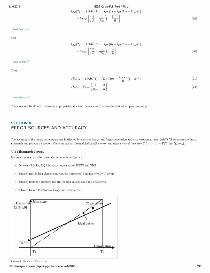
SECTION V.ERROR SOURCES AND ACCURACY
The accuracy of the measured temperature is affected by errors on and generation and on measurement part (ADC). These errors are due tomismatch and process dispersion. There impact can be modeled by offset error and slope error of the curve in (figure 5).
V.1 Mismatch errors
Mismatch errors can affect several components on figure 3:
Between RO, R1, R2 it impacts slope error on IPTAT and VBG
between R2R ladder elements introduces differential nonlinearity (DNL) errors
between Bandgap resistors and R2R ladder causes slope and offset error
between I0 and I1 introduces slope and offset error.
Figure 5: Slope and offset errors
IPTAT VREF
C[0 : n − 1] = F(T)

9/16/2015 IEEE Xplore FullText HTML :
http://ieeexplore.ieee.org/xpls/icp.jsp?arnumber=4449483 8/13
But in practice, the most important errors are due to active circuits offsets:
Comparator offset causes offset error.
It must keep it lower than 1/2LSB
View Source
Increasing R3 reduces the sensitivity to this offset, however this increases the opamp settling time, which must remain lower than one SAR clock period.
Subtractor OpAmp offset causes slope and offset error. Indeed, this offset causes Vp to differ from , which in turn affects both zero level andfullscale of the DAC. With and offset of 2mV, the slope error will not exceed 0.1%.
BandGap OpAmp offset is the most critical error source since it is directly added to and applied to R0. is proportional the voltage acrossR0, so an additional current error will be measured:
View Source
be is in the order of 70mV, thus will be a large source of error, furthermore offset can drift in temperature. However, the circuit has beenimplemented without chopping and calibration but relies on very good matching properties of our process, using large enough devices. In addition VREFwill also be affected, but with the same sign as the PTAT current thus mitigating this effect.
View Source
V.2 Systematic Process errors
in (4) will be affected by current gain variations which has been found to be the largest systematic source of error. Polysilicon resistor variation willhave only a secondorder effect by changing the current density.
V.3 Digital calibration
As offset errors are temperature independent, they can be subtracted from the output with a one point calibration:
| | ≤V COMPO−
IDA × R3CLSB
2(23)
VREF
= 1.2VVREF
ΔV be IPTAT
= (1 + )IPTAT
R1R2
Δ +VBE V BGo−
R0
= (1 + ) (1 + )IPTAT
R1R2
ΔVBE
R0V BGo−
ΔVBE
(24)
ΔV V BGo−
= + (1 + )VRE offF−VREF
R1R0
V BGo−(25)
λPTAT

9/16/2015 IEEE Xplore FullText HTML :
http://ieeexplore.ieee.org/xpls/icp.jsp?arnumber=4449483 9/13
Figure 6: Offset removal in digital
Before calibration (correction code=0):
View Source
If calibration is done at temperature , and measured code (uncorrected) at is , the correction code is .
The code after this calibration for an other temperature T is:
View Source
The temperature error is the .
We can note that this error increase with the difference between operating temperature and . So the ideal point of calibration is the middle of theoperating range (T0+T1)/2.
C(T ) = T0 + 0ffset + (1 + slop )(T − T0)eerror (26)
Tm Tm Cm −Tm Cm
C(T ) = + (1 + slop )(T − )Tm eerror Tm (27)
Slop (T − )eerror Tm
Tm
SECTION VI.EXPERIMENTAL RESULTS
The temperature sensor has been designed and fabricated in ST's 90nm and 65nm CMOS processes. The typical temperature range covered is 127 degreeswith 7 bits. This was chosen as a tradeoff between area and performance, with 1 LSB/K, the A/D conversion accuracy is better than the absolute sensoraccuracy due to analogue nonidealities depicted in section V. This was the optimum, as adding an extra bit of resolution not only adds an extra resistorelement but halves the mismatch budget on resistors, as the binaryweighted ladder is not intrinsically monotonic. Very careful layout techniques have beenemployed to merge the R2R array and the Bandgap resistors ladders to optimize D/A range to Iptat range mismatch.
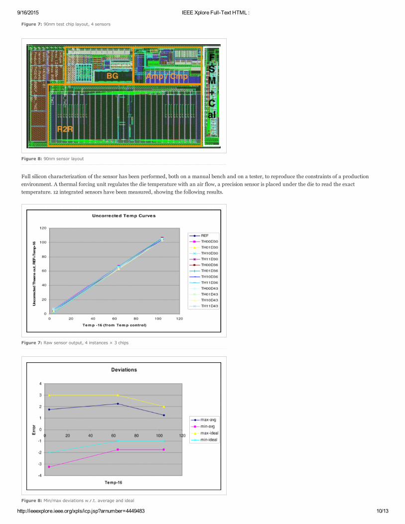
A dedicated test chip was designed, with different orientations of the same sensor, also allowing automatic tiling on some instances only, to explore possibleimpact on performance. The test chip layout is shown hereunder, with four sensors
9/16/2015 IEEE Xplore FullText HTML :
http://ieeexplore.ieee.org/xpls/icp.jsp?arnumber=4449483 10/13
Figure 7: 90nm test chip layout, 4 sensors
Figure 8: 90nm sensor layout
Full silicon characterization of the sensor has been performed, both on a manual bench and on a tester, to reproduce the constraints of a productionenvironment. A thermal forcing unit regulates the die temperature with an air flow, a precision sensor is placed under the die to read the exacttemperature. 12 integrated sensors have been measured, showing the following results.
Figure 7: Raw sensor output, 4 instances × 3 chips
Figure 8: Min/max deviations w.r.t. average and ideal
9/16/2015 IEEE Xplore FullText HTML :
http://ieeexplore.ieee.org/xpls/icp.jsp?arnumber=4449483 11/13
FOOTNOTES
"No Data Available"
REFERENCES
1. ISSCC Digest of technical paper, vol. 50, feb, 2007, James & AlShow Context
2. IEEE JOURNAL OF SOLIDSTATE CIRCUITS, vol. 33, no.7, JULY, 1998, "A SwitchedCurrent SwitchedCapacitor Temperature Sensor in 0.6um CMOS", MikeTuthill & Al
Show Context
3. A. Bakker, J. H. Huijsing, "Micropower CMOS temperature sensor with digital output", IEEE J. SolidState Circuits, vol. 31, pp.933937, July, 1996Show Context
4. "A CMOS Smart Temperature Sensor With a Inaccuracy of 0.5 C From 50 C to 120 C", IEEE JOURNAL OF SOLIDSTATE CIRCUITS, vol. 40, no.2, FEBRUARY,
The sensors produce an accurate output, with little dispersion from instance to instance on the same chip, showing no effect of orientation and tiling, andno significant dispersion from chip to chip. The worst deviations observed on 12 sensors are plotted on figure 8, showing a deviation of +3/2 degreescompared to ideal, without calibration. The measurements cover a temperature range of 20 to 120 degrees, 16 degrees have to be added to the figures onthe graphs, because the digital correction of the output (5 bits adder) was set to zero during these measurements without calibration.
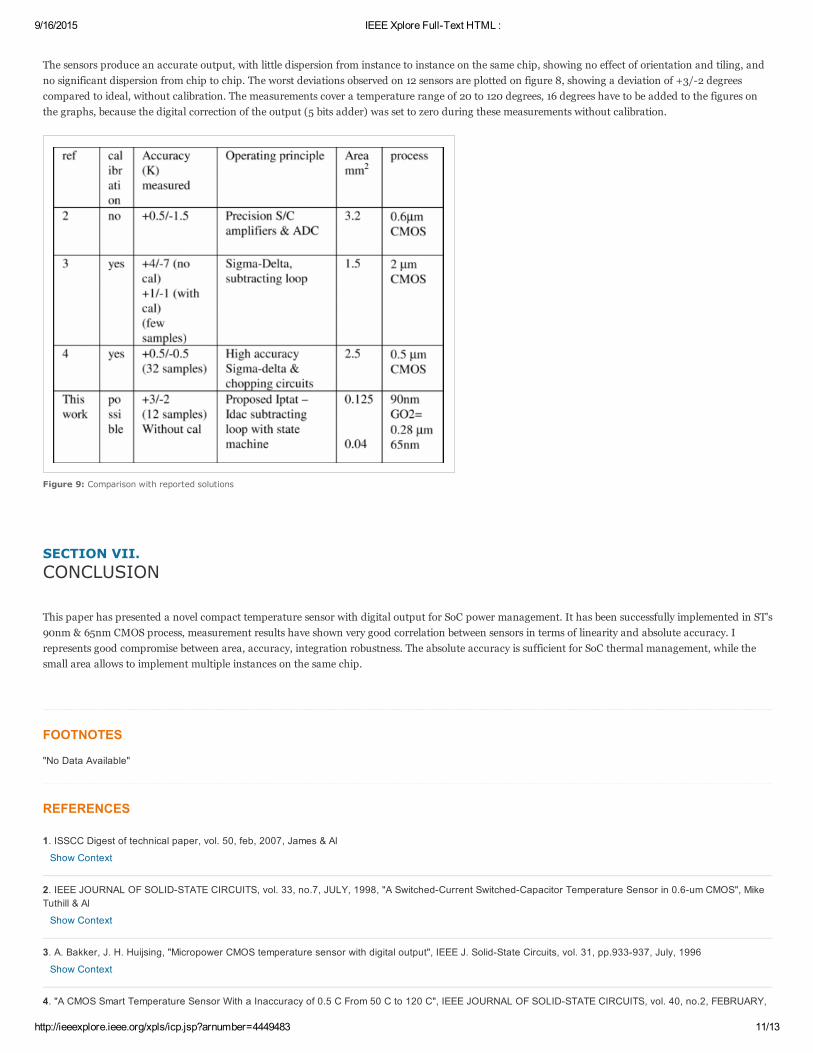
Figure 9: Comparison with reported solutions
SECTION VII.CONCLUSION
This paper has presented a novel compact temperature sensor with digital output for SoC power management. It has been successfully implemented in ST's90nm & 65nm CMOS process, measurement results have shown very good correlation between sensors in terms of linearity and absolute accuracy. Irepresents good compromise between area, accuracy, integration robustness. The absolute accuracy is sufficient for SoC thermal management, while thesmall area allows to implement multiple instances on the same chip.

9/16/2015 IEEE Xplore FullText HTML :
http://ieeexplore.ieee.org/xpls/icp.jsp?arnumber=4449483 12/13
2005
Show Context
AUTHORS
Lionel VogtNo Bio Available
Youness CharaNo Bio Available
Hicham OuannaniNo Bio Available
Maria NazihNo Bio Available
CITED BY
None
KEYWORDS
IEEE Keywords
Temperature sensors, Energy management, Voltage, Temperature dependence, Calibration, Energy consumption, Circuits, CMOS technology, Photonic band gap,Sensor systems
INSPEC: Controlled Indexingtemperature sensors, CMOS integrated circuits, systemonchip
INSPEC: NonControlled Indexing
size 65 nm, integrated temperature sensor, SoC power management, CMOS temperature sensor, analogue to digital conversion, power consumption, size 90 nm
Author KeywordsAnaloguetodigital conversion, Temperature Sensor, Temperaturedependant Source
CORRECTIONS
None

9/16/2015 IEEE Xplore FullText HTML :
http://ieeexplore.ieee.org/xpls/icp.jsp?arnumber=4449483 13/13
IEEE Account
»Change Username/Password
»Update Address
Purchase Details
» Payment Options
»Order History
» View Purchased Documents
Profile Information
»Communications Preferences
» Profession and Education
» Technical Interests
Need Help?
»US & Canada: +1 800 678 4333
»Worldwide: +1 732 981 0060
»Contact & Support
A notforprofit organization, IEEE is the world's largest professional association for the advancement of technology.© Copyright 2015 IEEE All rights reserved. Use of this web site signifies your agreement to the terms and conditions.
Personal Sign In Create Account|
About IEEE Xplore Contact Us| Help| Terms of Use| Nondiscrimination Policy| Sitemap| Privacy & Opting Out of Cookies|