ies electronics 2011
DESCRIPTION
business modelTRANSCRIPT

-fxa.m_, 20.11
DO NOT OPEN THIS TEST BOOKLET UNTIL YOU ARE ASKED TO DO SO
T.B.C. : P·RSR·L·RGA Test Booklet Series
Serial
TEST BOOKLET ELECTRONICS &
TELECOMMUNICATION ENGINEERING'--------' Paper I
Time Allowed: Two Hours Maximum Marks : 200
INSTRUCTIONS
1. IMMEDIATELY AFTER THE COMMENCEMENT OF THE EXAMINATION, YOU SHOULD CHECK THAT THIS TEST BOOKLET DOES NOT HAVE ANY UNPRINTED OR TORN OR MISSING PAGES OR ITEMS ETC. IF SO, GET IT REPLACED BY A COMPLETE TEST BOOKLET.
2. ENCODE CLEARLY THE TEST BOOKLET SERIES A, B, C, ORDAS THE CASE MAY BE IN THE APPROPRIATE PLACE IN THE ANSWER SHEET.
3. You have to enter your Rol! Number on the ,----------------, Test Booklet in the Box provided alongside. DO NOT write anything else on the Test Booklet.
4. This. Test Booklet contains 120 items (questions). Each item comprises four responses (answers). You will select the response which you want to mark on the Answer Sheet. In case you feel that there is more than one correct response, mark the response which you consider the best. In any case, choose ONLY ONE response for each item.
5. You have to mark all your responses ONLY on the separate Answer Sheet· provided. See directions in the Answer Sheet.
6. All items carry equal marks.
7. B~fore you proceed to mark in the Answer Sheet the response to various items in the Test Booklet, you have to fill in some particulars in the Answer Sheet as per instructions sent to you with your Admission Certificate.
8. After you have completed filling in all your responses on the Answer Sheet and the examination has concluded, you should hand over to the Invigilator only the Answer Sheet. You are permitted to take away with you the Test Booklet.
9. Sheets for rough work are. appended in the Test Booklet at the end. 10. Penalty for wrong answers :
THERE WILL BE PENALTY FOR WRONG ANSWERS MARKED BY A CANDIDATE IN THE OBJECTIVE TYPE QUESTION PAPERS.
(i) There are four al~ernatives for the answer to every question. For each question for which a wrong answer has been given by the candidate, one·third (0•33) of the marks assigned to that question
. will be deducted as penalty.
(ii) If a candidate gives more than one answer, it will be treated as a wrong answer even if one of the given answers happens to be correct and there will be same penalty as above to. that question.
(iii) If a qu~stion is left blank, i.e., no answer is given by the candidate, there will be no penalty for thcit question.
DO NOT OPEN THIS TEST BOOKLET UNTIL YOU ARE ASKED TO DO SO
www.examrace.com

I.
2.
3.
F'or -..mouth -1nd rehable operation of an 14. amphfh.~r U~-'-Hlr.; H.JT, tt is ~1ere~~::-;acy t.hat tht.! ,
cl.n'Uit mud bl· ;.n·npcrly deMi{.,.Yflcd frorn the polnr: of Vlt"W of bias .:;tabill7.ation, t>t-~:atp-.;.~
I.
2.
3.
R ... '"·~J'>t· :-t;:t.t.ur•·t.ion current J 1 '- ._. 'V cuI
incr~ast-·~ w1th d:-,e i.n temperature.
V I:W d(~cn-·a:>Ps with J"bc in ternpl·raturc. !
or l~ r.han~{e!J with chdn!~t· of\
and tt•placernent. of the \
ht .. ~ L
tempt~r·at.·.trt>
tran.-;1:-;tot I hl- r: ur f} t~hungel:l. with chungt· in I (;ol.l.e(~tor· ,;upply volta~te.
(a) 1, ~ and J only
'b) I.~ and 1 only
,c: 2 ::s and ·1 only
:d) 1 ~' :-; and ·1
lnt("~r~:->t" ma~·n..r.i~,.- field may be prudw~ed coil by ui':)H~g l::i
~m·ma! met:-d with a laq•t. number
tunt~ d.nd .->t·ndJ:ng· a targe tucrtm:
;bl Type I Htp!-~tTundu<~t.or \>\it~ .1 idr~~t!.
ou.mb~r .A turn:"! and ~endn:tg a lar~e
,. .. u~-rr.·nt
Typ~-1 l ~.upt!rcundth·tor wi.th " large ou.mbt·r flf tll1'DI"i and ~ending a large 1:
.ru:rrt·ot I
l'jp<-·11 !l.UJ.lt•rconductor wi.th h:trge i6,
:1 I nu.mCu-r of t.urn:.; but ~im~ting ~h~"' t:orrent density below a. iTjtlC'ul va}ue I
The urnt et<U of u certmn type of Cl')o-st~tl J.;i 1
defined by t.hn·~: vedors a, b and c.
Tht:~ n·~,·.tor.-; an .. nluf,.larly pr=·rpPndJ('Uhu 1 but I a -1 b ~ c. Th~:: l.T}"-'t::ti ..;t.r·I.J.Ct-.lre ia
(d 1 ~lunudin1c
P·RSRLRGA ( 2 Al
Riw5.ing lr· usl~d in tra :rurition amplifier·} to
I.
2.
3.
4.
StabHize the !tpt~r~itln~~ point d.!!ain:d
temperature variuttonM.
Place the operating point in thl' bnl:!ar
region of the charadcrtstic~.
Make U 1 ;_) and leu of the :..ransistor independent of ~ern pen~..t.ure vuridt.l.Ons.
Reduce distort1on and lnc~reaoe C:ynandc range:<.
'o.J 1, ~. :l and 4
{b) I, 2 and 4 only
\C) 1. \! and 3 unly
(d) ~. 3 and 4 only
The J""e!$i.:' t.ivity of a m~:·ta.l i., a fur:.ct.ion of temp(:rature becau:H-·
~ cl: Tht~ dedron temperature
dee:si:-:y
(b) The eh·ct.ron temperature
;~a:-: density lfari~r-: with
(l') Tht' lattict"~ vibrJt.J.Ori mcn·aMeH With tern pt:·ratur~
(d; Co!Ji:sion ut ~h··d ronM m~Tt':l:-.;e.s a,..,
temperature i:ncn~:J::-;t:.-1
An. inn-in.:-:.1c ~emu~onductor haii tht; t~:>Uowing prop~:·rbP>!. :
1. ltr; Pl.ectroo nmcent ratwn equal~ it:i holtrontentratwn _
2.
3.
~a;
(bl
(c)
(d;
Its carril'r· den~it.)' incrtast.i with tern peraturtc>~
Its conduetivoty d.ecrea:;e~; with t~rn peratur-e
1 "} .~ drld 3
~ and 3 only
and J onf:y
and 2 only
www.examrace.com

7 . .
8.
. 9.
A 'hole' in a semiconductor has
1. Positive charge equal to the electron charge.
2.
3.
4.
Positive mass equal to the mass of the electron.
An 'effective mass' greater than the effective mass of electron.
Negative mass and positive charge. equal to the charge in nucleus.
(a) 1, 2, 3 and 4
(b) 1 and 3 only
(c) 2 and 4 only
(d) 3 and 4 orily
A CE amplifier has an unbypassed emitter resistance of 0·5 kQ and a collector load of 5 kQ. The B of the transistor is 100 and it is operating at 1 rnA. The voltage gain of the stage at mid band will be of the order of
(a) 200
(b) 100
(c) 10
(d) 50
10.
11.
A common emitter transistor amplifier has a
collector load of 10 kO. If its hfo = 100 kQ 12.
and hie = 2 kO (hre " h 00 " 0), the voltage amplification of the amplifier is nearly equal
to
(a) 500
(b) 200
(c) 100
(d) 50
P-RSR-L-RGA ( 3 - A )
The · free electrons in a metal follow the kinetic theory of gases and the following statements are made about their properties :
1.
2.
The velocity of all the electrons is equal.
The electrons have distribution ranging infinity.
a from
velocity zero to
3. The average velocity of electron gas is
proportional to .JT (T = temperature).
4. The maximum velocity of electrons is proportional to T.
Which of these statements are correct? (a) 1, 2, 3 and 4
(b) 1 and 3 only
(c) 2 and 3 only
(d) 3 and 4 only
Using transistors,
1. Class-A power amplifier has a minimum efficiency of 50%.
2. Class-B push-pull power amplifier gives rise to crossover distortion.
3. Class-AB push-pull power amplifier has higher efficiency than Class-B push-pull amplifier.
4.
(a)
(b)
Class-C power amplifier is used with tuned load amplification. 1, 2, 3 and 4 2 and 4 only
(c) 3 and 4 only
(d) 1 and 2 only
generally for RF
A material shows spontaneous magnetization. This is due to
1. Weiss molecular field.
2. Cooperative effect among dipoles.
. 3. Cooperative effect among domains.
4. Absence of applied magnetic field.
(a) 1, 2, 3 and 4
(b) 2, 3 and 4 only
(c) 1, 2 and 3 only
(d) 1, 2 and 4 only
www.examrace.com

13. Mat.,rial• in which the permanent d1pole" 16. int,ract with each other so heavily that they tend to align parallel to each other are called
(a} Ft·rromagnetic
tbl fi't··rrimagnetic
k;· Parama~~netlc
(d) Anti~ferromagnctic
14. A type f ~uperconductor is
1. A conductor of tnfinite condu.ctivr:ty at all temperature•. 17.
15.
2. A conductor with very large conductivity bdow a c·ritical temperature.
3. A material showing susceptibility -' 1 below (:ritical tt·mperature.
A perf.,ct conductor having conductivity drastically reduced by a critical current.
'a' I. 2 and 3 only
<b! 2, 3 and 4 only
c: 1, 2 and 4 only
\d; 1. 2, 3 ::lUd 4
In an RC coupled transistor amplifier
L
2.
3.
Low~fTt·quency re:sponse by coupling capacitors.
1-ligh-fJ-pqu~ncy response by jun(·tion capacitance~:~:.
Mid-&t->quency response by both couplmg capacit.anct.-'!.'"'.
(al 1 and <! only
(b l 1 and :l only
(ci i and 3 only
(d) 1, 2 and 3
is dekrmined
is- determined
is determined and junction
18.
P-RSR-L RGA ( 4 A l
Ti i:-; difiU.sed i.ntu a wt.•:t defined region of
LiNb03 cry~tal. The followin1r effects '"" expected:
1. An optical waveguide L~ ~~Jnned Ul the region containing Ti.
2. Ti containing r·egion has a larger refractive index than in undoped region
3. Ti containing r-egwn ha:-; ii :.ower refractive index than in undoped region.
(a) 1, 2 and 3
ChJ I and 3 only
lc) 1 and 2 only
(d) 2 and 3 only
RF. LF
r---r r ~~~ ·~r~ --r~~ f I o-- - l...__ ....._ __ ____.... -l
The inductance Ly and n~~istanc~ RF in the above Circuit iB u.sed for
{a) Low frt~quency c·ompt:msat.wn onJy
Ch) High frequency compensation only
(c) Both low frequency »nd high frequency compenKation
(d) Increasing mtd fn·quenc.v gain without afftcting tht cut off frequenc:ie.o;
o-
o-
' c~-±
·- .1._
Cc .,--jf-
~Rc
• ~ R,
1 I ·. I
1,--' ~-.-lT., - -R,
In tht! above c1rcuit the optimum low frequency compent-.ation i>:l obt.aint>d when
(a) c,R1 R],/\
(b) C1R
1 ., CcR,
(c) C1 lRc II R1 1 ~ CcRi
(d) c, lRc II R1 : ~ R<:C}
www.examrace.com

19. +Vee
The amplifier circuit shown in the figure is
ah example of
(a) Voltage series feedback
(b) Voltage shunt feedback
(c) Current series feedback
(d) Current shunt feedback
20. Tne peak output of a tuned amplifier is at
6 MHz and has quality factor of 60. The
bandwidth and 3 dB frequencies shall be
(a) 100 MHz, 6·05 MHz and 5·95 MHz
(b) 6 MHz, 9 MHz and 3 MHz
(c) 600 kHz, 6·6 MHz and 5·4 MHz
(d) 100 kHz, 6·05 MHz and 5·95 MHz
21. On applying an electric field of intensity
10 V /em across a semiconductor at a certain temperature the average drift velocity of free
electrons is measured to be 70 m/s. Then the electron mobility is
(a) 7 x 104 cm2 /Vs
(b) 700 cm2/Vs
(c) 7 m2/Vs
(d) 700 cm/Vs
22. Consider the following statements with regard to semiconductors :
1.
2.
3.
4.
In n type material free electron concentration is nearly equal to density of donor atoms.
1 part in 108 donor type impurity added to Ge improves its conductivity at 30'C by a factor 12.
Phosphorus is an example of .n type impurity.
Conductivity of Si is more sensitive to temperature than Ge.
Which of these statements are correct ?
(a) 1, 2 and 3 only
(b) 1, 3 and 4 only
(c) 2 and 4 only
(d) 1, 2, 3 and 4
23. The diffusion constant for holes in silicon is
13 cm2/s. What is the diffusion current if the
gradient of the hole concentration
dP =- 2 x 10¹⁴ holes per cm3 per em ? dX
(a) - 0·416 rnA
(b) - 3·2 X 10-5 A
(c) 32 flA
(d) 0·416 rnA
P-RSR·l·RGA { 5- A I
www.examrace.com

24. Given that at room temperature, the volt i 27.
equ1vulent of tt~mp~rature VT ·--- 26 mV, hole j
25.
26.
mobility ~,. ~c 500 l'm2/Vs and the life ti.me or: holes i>< 130 ns, in a sample of n-.type •ilicon I bar t~at i:-:. t··xposl'd to radiation at one l"r.Hl at
!ow-injt·ction J.evel. what is tht: diffu:-~ion
:.enbrth t.f hoi e~ ?
(a) 1300 microns
(b) lOO Arm•t.rongH
(c) l69 m1crons
(dl l 00 mi.;ron~
The function (A &.:· HJ l8 to be realized uBl.ng I only 2··input i\;AND gates. The minimum
numb~r of 2 input NA..'ID gates required for
such h realization is
{a,' J
(b) 4
(c) 5
(d.' 6
2
!--~~ '
-.-~.--~ -~ .. !
:1 ~-B
Con~ider a . ..;em~condud.or carrying current. and placed in ~::~ ~ran~vt·r8e magnetic fi~ld B~ a~ shown ahovt'. The rrteasured potential acrOsti t and 2 ~urfaces is positive at 2_ What ie the type of material ?
(a,1 (ntrintotk Si material
t.bJ n .. ' YPt' ,::emiconductor mttterial
,cl p· type c.t-:m.H.;;onductor materia!
{d' Nu such condul)ion can he drawn
28.
29.
P-RSR-L HGA ( 6 A I
A 700 m W maximum power dissipation diode
at 25•c has 5 mW/"l: de-rating factor. If the forward voltuge drop remains constant at 0·7 V, the maximum forward current at 65•C IS
(a) 700 rnA
(b) 714 mA
(c) I A
(d) I rnA
r3V [
0
-~~-v 1¥ i
• I-? . . ·~~ 3 v
?
For the circuit shown above. using idea! diode, tht' values of voltagt:'! und current are
(a) ~ 3 V and 0·6 mA
(b) 3 V and 0·0 mA (c) 3 V and 0·6 rnA
(d) ~ 3 V and 0·0 rnA
Consider the following ::>tat.ement~
1. The radiation falling on a photodiodc is primarily a minority earner injt~ctor.
2. The short~circuit currt~nt of a reverse biased photodiode cmder illumination varie~ exponentially with light intensity.
3. The photovoltaic emf of an open··circuited photodiode varies logarithmically with the light-generated short-circuit current.
4. The spectral response of a photodiode does not depend upon thP frequency of the incident light.
Which of these statementcs are correct 'J
(a) 1, 2, 3 and 4
(b) 3 and 4 only
(c) 1 and 2 only
(d) 1 and 3 only
www.examrace.com
30. Match List I with List II and select the correct 33. answer using the code given below the lists :
List I List II
A. At peak 1. Low tunneling point current
B. At valley 2. Zero tunneling point current
c. Reverse bias 3. High diffusion region curient
D. Beyond valley 4. High tunneling point current
Code":
The collector and emitter current levels for a transistor with common base de current gain of 0·99 and base . current of 20 !!A are respectively
(a) 2 rnA and 1·98 rnA
(b) 1·98 !!A and 2 rnA
(c) 1·98 rnA and 2 rnA
(d) 2 rnA and 1·98 !!A
A B c D 34. The difference between PLA and ROM is
31.
(a) 3 2 4 1 (b) 1 2 4 3 (c) 3 4 2 1 (d) 1 4 2 3
A half-wave rectifier has an input voltage of 240 V rms. If the step-down transformer has a turns ratio of 8 : 1, what is the peak load voltage ? Ignore diode drop.
(a) 27·5 V
(b) 86·5 v (c) · 30·0 V
(d) 42·5 v 32. Consider the following statements :
1. The efficiency of a light emitting diode (LED) decreases with the injected current.
2. The efficiency of a LED increases with a decrease in temperature.
3. The light· emitted is concentrated near the junction because most of the carriers are within a diffusion length of the junction.
4. Light is emitted in a LED when electrons move from the valence band to the conduction band.
Which of these statements are correct ? (a) 1, 2, 3 and 4
(b) 1 and 2 only
(c) 3 ~nd 4 only
(d) 2 and 3 only
35.
P-RSR-L-RGA I 7- A)
(a) PLA is sequential, ROM is combinational
(b) PLA is c~mbinational, ROM is sequential
(c) PLA economizes min-terms to functions
on the number of implement Boolean
(d) PLA has fixed AND array, ROM has fixed OR array
Consider the following statements :
1. In a silicon controlled rectifier (SCR), if the cathode gate is reverse-biased, then the SCR cannot fire at all.
2. The turn-on time of an SCR increases with temperature.
3. After an SCR is turned on, it can. be made to turn off again by reverse biasing the gate.
4. Gate recovery time is the minimum time that the . anode voltage must be maintained below holding voltage V H to turn off the SCR.
Which of these statements are correct ?
(a) 1, 2, 3 and 4
(b) 1 and 2 only
(c) 2 and 4 only
(d) 3 and 4 only
www.examrace.com

36. Which one of the following statements is 39. Consider the following statements about correct aMut SCR ? CMOS :
37.
38.
(a) SCR ;, constructed using an npn and
pnp transistor by connecting base of one
transistor to collector of the other transi.stor.
(b) To >•witch off an SCR, gate current must
be r<'duced below certain threshold value.
(c) Higher levels of gate currents in SCR cause i_t t.o conduct at lower:
(d) Thoe higher the gate current in SCR, the I higher the holding current to switch off_
The p-type epitaxial layer grown Dver an 1
n-type substrate for fabricating a bipolar i tn1nsi~tor will function a8
(u ~ The collPrtor of a p-n-p trarlliistor
(b) The hur>e uf an n-p·,n transistor
(c) The ?mitter of a p-n··p transistor
(d) The collector contad for a p-·n-p transi~tor
The biab:_ng of an IC BJT is done following bi.a~ing ){Cherne :
{a; Potential·d)"'ider hiafiing scheme
(b) i<,ixed biuoing .':icheme
(c) Current mirr·or biaNing scheme
:d) Collector to base feedback ;:;:cheme.
by the
biasing
I
!40.
i i I I '
P-RSR-l-RGA { 8 A I
L CMOS logic inverter has maximum signal swing of 0 V to Voo.
2. The output signal swing is independent
of exact value of aspect ratio and other device parameters.
3. It is a fast switching device with wide noise margins.
4. It has zero input re<istance and infinite output resistance.
Which of these statements are correct ?
{a) 1, 2, 3 and 4
(b) 1, 2 and 4 only
(c) 2, 3 and 4 only
(d) 1. 2 and 3 only
Match List I with List II and select the correct answtr using the code given below the lists :
List [
A. LED
B. LCD
C. Opto couplers
D. Photodiode
1. I<;Jectrical isolator
2. Forward biased
3. Light reflectors i tranrlmitters
4. Rever-t>e biased
Code:
A B C D
(a) 4 1 3 2
(b) 2 1 3 4
(c) 4 3 1 2
(d) 2 3 I 4
www.examrace.com

41. Given a unity feedback system with 44. Unit step response of the system described by difference equation y(n) + y(n - 1) = x(n)
is G(s) = K , the value of K for damping s(s+6) ·
ratio of 0·75 is
42. System is said to be marginally stable, if
(a) Gain crossover frequency > Phase crossover frequency
(b) Gain crossover frequency =
Phase crossover frequency
(c) Gain crossover frequency <
Phase crossover· frequency
· (d) Gain crossover frequency * Phase crossover frequency
43. System transformation function H(z) for a
discrete time LTI system expressed in state
variable form with zero initial conditions is
(a) c (zi - A)-1 b + d
(b) c Czi- Ar1
(c) (zi- A)-l z
(d) (zi- A)-1
(a) (z + 1) (z -1)
45. Which one of tl)e following relations is not correct ?
(a) f(t) li(t) = f(O) o(t)
~
(b) f f(t) o(T) dT = 1
~
(c) f o(T) d(T) = 1
· (d) f(t) 1\(t - T) = f(T) 1\(t - T)
46. A family of constant N circles has the centre as
(a) X = 1 and Y = 2 N
(b)
(c)
(d)
1 X = - - and Y = 4 N
4
1 andY=
1 X=--
2 4N
1 X=-- andY=
1 2 2N
P-RSR-l-RGA I 9- A)
www.examrace.com

47. 10Q A
50V 10Q
B
Consider the circuit shown above. The portion of the circuit left to the terminals AB can be replaced by
5Q A
1. 25V z
B
A
2. 20V
B
A
3. 1A
B
48. f(t)
Laplace transform of the function f(t) shown
in the figure is
(a)
(b)
(c)
(d) ~ [1 + e0·5 s]2 s
49. Time constants of R-L and R-C circuits are respectively :
A R = 1 Q; L = 1 H and C = 1 F r---.--.o:.....~.:..,
(a) 1 sec and 1 sec 4. 5Q
(b) 1 sec and 2 sec B
(a) 1 and 2 only (c) 2 sec and 3 sec
(b) 2 and 3 only (c) 1, 2 and 3 only (d) 2 sec and 4 sec
(d) 1, 2, 3 and 4
P-RSR-L-RGA { 10- A}
www.examrace.com

50. Which one of the following gives the V-I 51. characteristic of an ideal voltage source ?
v
(a)
v
(b)
i
SQ vv
4Q
12 v --:::--
The circuit shown in the figure is m steady
state before the switch is closed at t = 0. The
current i 8(0+) through the switch 1s
(a) 1/3 A
(b) 2/3 A
(c)· 1 A
(d) 0 A
52. Consider the following statements
v~---------------
(c)
v
(d)
i
P-RSR-L-RGA !11-AI
1.
2.
3.
4.
Voltage across a capacitor cannot change abruptly.
Voltage across an inductor cannot change abruptly.
Current through a capacitor cannot change abruptly.
Current through an inductor cannot change abruptly.
Which of these statements are correct ?
(b) 2 and 3 only
(c) 3 and 4 only
(d) 1 and 4 only
www.examrace.com

53.
54.
Match Li>t I with List II and seled the 155. correct ant-~wer using thP- code given below the li•t• :
J,i.<l I List II
A. Superpol:.>ition l. Impedance matching theorem in audio circuit..:;
B. The"eoin~!i 2. Linear bilateral theorem networks
C. Kirchhoff's 3. Ln·ge network in voltage and which currents in curr~nt. ·laws few elernents to be
detennined
D. Maximum 4. CuJTents and puw~r tram"fer voltages in all theorem branches nf a
network
Code:
A B c D
{a; 1 4 3 2
(b) 2 4 a (c) I a 4
(d) 2 ::1 4
A 2Q B .~ -r il,ov lOAcp ~2 ~l
.J i.
The current through the branch AB in the figure shown i~
(a) 10 A, from A to B
(b) 10 A, from H t.o A
(cl 0
(dJ 20 A, from B to A
56.
P·RSR-L·RGA ( 12 A )
In the circuit ohown, the ;;witch is opened at
t -·- 0. The circuit is
(a) Critically dam pcd
(b) Under-damped
(c) Over-damped
(dl Undamped
In the circuit shown~ the initial current 10
through the inductor is givf'n in the figure_
The initia;_ value of t.ht:> voltage across the
inductor V0{0+) is
(a) 12·5 V
(b) 5·0 v
(c) 10·0 V
(dl 0·0 v
www.examrace.com

57.
58.
lOQ 8 11
4Q 11 +
lz
v1) 5Q
) V2
For the network shown in the figure, Y 11 and Y 12 are, respectively
(a)
(b)
(c)
(d)
i
3 mho and
50
3 mho and -
50
3 mho al)d
50
3 50
mho and
11
N
1 mho
30
1 mho -
30
1 mho --
30
1 30
mho
12
i A two-port network satisfies the following re1ations :
4 I1
+ 8 12 ; 2 V 1
8 11 + 16 12 ; v 2
1. The network is reciprocal
2. zll ; 4 and z12 ; 8
3. z21 ; 8 and z22 ; 16
4. zll ; 2 and zl2 ; 4
Which of these relations are correct ?
(a) 1, 2, 3 and 4
(b) 2 and 3 only
(c) 3 and 4 only
(d) 1 and 2 only
59.
60.
P-RSR-L-RGA 113-A)
11 12 Vz
+
> ~50Q
N
_\)Vs < 10 kQ
In the circuit shown, 2-port network N has
Z11 ; 103 n, Z12 ; 10 n, Z21 ; - 106 n and
Z22 ; 104 n. The current gain .!... is 11
(a) -50
(b) + 50
(c) + 20
(d) - 20
: 1 Q 3 Q
In the 2-port network shown in the figure, the value of Y 12 is .
(a)
(b)
1 . mho 3
+ .!_ mho 3
(c) - 3 mho
(d) + 3 mho
www.examrace.com

61.
62.
~·or " n~twork tran•fer function H(•l _ Pis), Iss. ~(s} ;
where Pl.;) and Q(•l are polynomials in S,
Tht· degree of P(s) and Q(s} .are same.
2. The degree of P(s) is always greater
t.han the degree of QC>).
3. Th~ degn•e of Piol is independent of the . dtf..'Tee of Q~:-o:1.
4. I
The maximum degree of P(s) and Qt.>) differ at most by one.
Which of t.hf':->l' statements are corrc.:ct '1
ibl 1. 2 and 3 only
lei I. ;l <>nd 4 only
(d) 2, 3 and 4 only
10 11 I F'
~- -- [ ---r- ----1 ~~-1
2H~V1 (sl
o- .-
The driving poinr im pedan(:e of the nL't.wurk ~
~~hown m figure is
1
(c) 10
·.d)
PRSR L-RGA I 14 · A I
L --o--- -o---~ ·+0
2. ------o--
3.
4. --· 0'
The valid pole- zero patkrnn for an RL
driving point impedance function, are
(a) I and 2 only
(b) 2 and 3 only
(c) 3 and 4 only
(dl 1, 2, 3 a"d 4
www.examrace.com
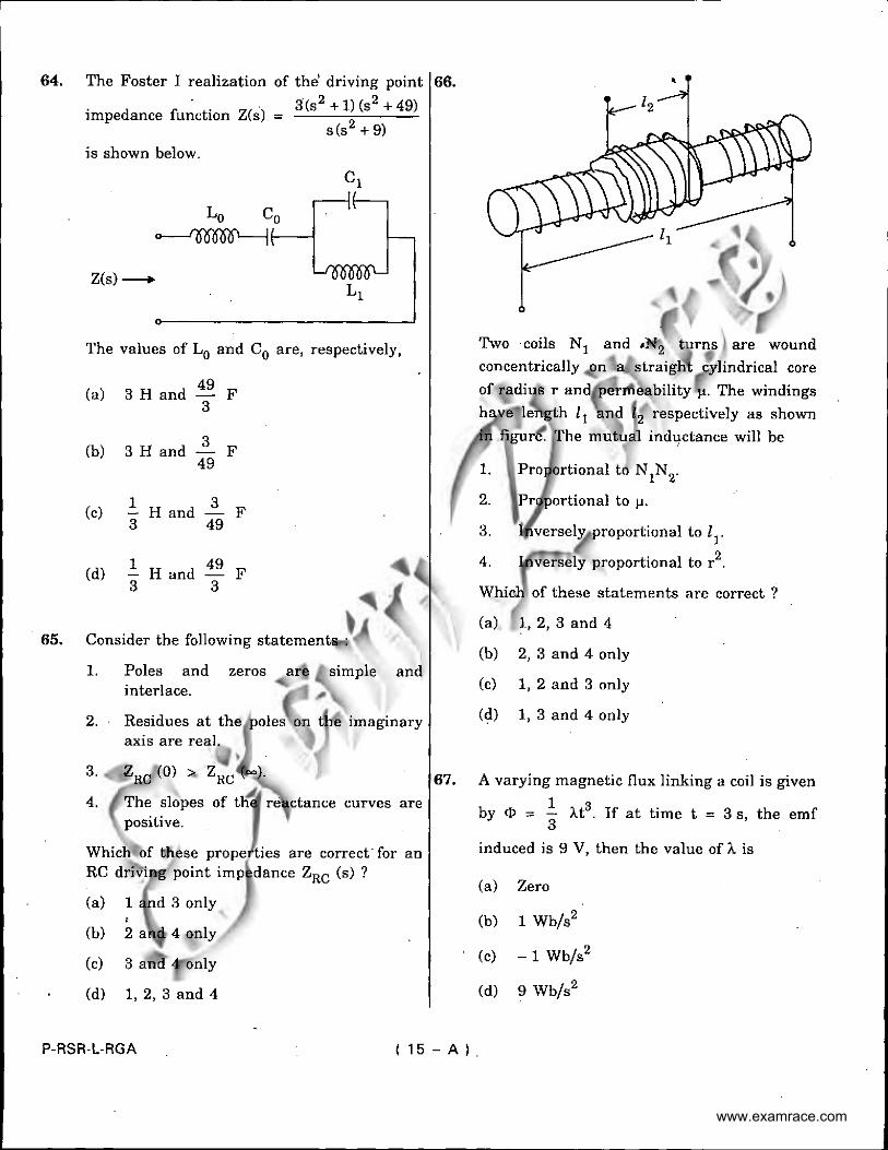
64. The Foster I realization of the' driving point 66.
3(s2 + 1) (s 2 + 49) impedance function Z(s) =
s(s2 +9)
is shown below.
Z(s)_.
The values of L0 and C0 are, respectively,
(a) 3 H and 49
F 3
(b) 3 Hand 3
F 49
(c) 1
Hand 3
F -3 49
(d) 1
Hand 49
F - -3 3
65. Consider the following statements :
1.
2.
3.
4.
Poles and zeros are simple and interlace.
Residues at the poles on the imaginary axis are real.
ZRC (O) > ZRC (~). 67,
The slopes of the reactance curves are positive.
Which of these properties are correct· for an RC driving point impedance ZRC (s) ?
(a) 1 and 3 only
(b) 2 and 4 only
(c) 3 and 4 only
(d) 1, 2, 3 and 4
P-RSR-L-RGA (15-A)
•
Two coils N 1 and •N2 turns are wound
concentrically on a straight cylindrical core
of radius r and permeability J.l. The windings
have length 11 and 12 respectively as shown
in figure. The mutual indl!ctance will be
1. Proportional to N 1N
2.
2. Proportional to J.l.
3. Inversely proportional to 11
.
4. Inversely proportional to r 2
Which of these statements are correct ?
(a) 1, 2, 3 and 4
(b) 2, 3 and 4 only
(c) 1, 2 and 3 only
(d) 1, 3 and 4 only
A varying magnetic flux linking a coil is given
by <I> = .!:. At8 If at time t = 3 s, the emf 3
induced is 9 V, then the value of A. is
(a) Zero
(b) 1 Wb/s2
(c) -1 Wb/s2
(d) 9 Wb/s2
www.examrace.com

68. If the p(Jkntla1, V - 1x + 2 vults, t.ht t"·lectr'i.l: 71. fl<'ld is
l~di 6 V/m
.b; l V/rn
(c) 4 V/m
\d: 4 u \ V/m
69. If th~~ l~urn_.nt element repre~enh~d oy
70.
4 ·" ro ~ a,. Amp~rn b placed
field of H ~ .5 "• A/m. the u
~a~ ~ .. o a_., mN
(c' :~ 0 1., ~"~~
10 a marm ttc
1 forct~ on the ~
72.
~!akh t_,;,, I w1th Liot ll and .;elect
correct an:-\Wt'T u~ing t.he code given t.elnw the :i::>t:-> :
Lf,f , A ~IMF
ll Magnetlt· tlux
(. ~ . H.dut~tanc~
D. PtrmeabiHty
Code:
A
• cl J
B
4
4
2
1
4
2
D
3
1
3
I.
2.
J.
4.
Li.•;l If
Condu~~tivi.ty
Electric current
~;MF
Ret>l::::-.r~anct·
P·ASRl RGA I 16 A )
Given that the electric flux density
D._,_ zp (co~~<!>) a, C/m:t.
The charge density at poinr. 1 '!. rr./4, 3) u~
(d) 3
(b) I
(c) 0·6
!d) 0·5 a,
Two die!Pctric media with permlttivities a and ,;'3 are separatPd by a charge-free
boundary as shown in figure, The electric
field intt.·n~ity nt rnedium ~ at pmnt P 1 has
magnitude E 1 and makes an angle o:t ....:. 60°
w1th the normaL The direcl.ion of the electric
field interu~ity at point P .!.' ..,_'l i~
(a) oin r '3 E ' ' " 1
\ 2
(b) 45''
{c) . ~ 1 I /3 g, '
co~ I . ~ ·~
' 2 '
(dJ 30"
www.examrace.com

,------
73. For no reflection condition, a vertically 75. polarized wave should be incident at the interface between two dielectrics having
74.
E1 = 4 and E2 = 9, with an incident angle of
(a) tan-1 (~)
(b) tan-1 (%)
(c) t -1 an (~)
(d) tan-1 (~)
Assuming that each loop is stationary and time varying magnetic field B, induces current I, which of the configurations in the figure are correct ?
1.
3.
Increasing
B
I
Decreasing
B
I
(a) 1, 2, 3 and 4
(b) 1 and 3 only
(c) 2 and 4 only
(d) 3 and 4 only
2.
4.
Decreasing
B
I
Increasing
B
I
76.
77.
P-RSR-L-RGA (17-A)
The electric field component of a wave in free space is given by
- 7 E = 10 cos (10 t + kZ) ay V/m.
Following is a list of possible inferences :
1. 2.
Wave propagates along ay Wavelength /.. = 188·5 m
3. Wave amplitude is 10 V/m 4. Wave number = 0·33 rad/m 5. Wave attenuates as it travels
Which of these inferences can be drawn from
E?
(a)
(b)
1, 2, 3, 4 and 5
2 and 3 only
(c) 3 and 4 only
(d) 4 and 5 only
An electromagnetic wave of frequency 3 MHz passes from vacuum into a dielectric medium
with permittivity E = 4·0. Then
(a) Wavelength is doubled and the frequency remains unchanged
(b) Wavelength is doubled and the frequency becomes half
(c) Wavelength is halved and the frequency remains unchanged
(d) Both the wavelength and frequency remain unchanged
Air
Water
A plane wave fs generated under water (E = 81 E
0 and fl = f1
0). The wave is parallel
polarized. At the interface between water and air, the angle a for which there is no reflection is (a) 83·88° (b) 83·66°
(c) 84·86°
(d) 84·08°
www.examrace.com

78. Tht: characteristic lrnpedance of TV rect.-lvi.ng ~ 81. Loading of a cable t.~ don~ tl}
79.
antenna cable b 300 n. [f the conductor•
are made of coppt~r 8eparated by air and are
1 rr~ m thic:k, what is the phase ve~odt.y and
pha•e constant when receiving VH~' channd i
3 (63 MHzl and VHF 69 (803 MHzJ ?
(a,\ l 32 rad/m and 17·82 rad/m
ib) 1·5:l rad/m and 16·!!2 rad/m
(c) 1·52 rad/m and 17·82 rad/m
ldJ 1·32 rad/m and 16·82 rad/m
If maximum and minimum voltap::.~s on a
tranr~miNs1on lint are 4 v ~nd 2 v r·espect.ively, VSWR i• ! 82.
(a) 0·.)
I, b) 2
' ... c"
\d) 8
80. An idf"al losslP~~'~ transmission l:me of
Z0 ·--· 60 ll is connected to unknown ZL If
SWR = ~. find ZL
(a) 240 n
(bl 480 n
(c) 120 U
(d) lOO U
P·RSRL·RGA I 18 A l
I. Increase ib~ inductancl'
2. lncn·aHe its IPakage resitltance
3.
4. Aclncve diti>tort.ionless cundition
(a) 1, 2, 3 and 4
(b) I and 2 only
(c) 2 and 3 only
(d) I and 4 only
Consider the foHuw)ng :,tat.vment.~ <Jbout the
Smith chart :
l_ A complete rev(1lut.lon ';J6U·':• arm~nd the
Smith chart n·pre,.<'nh a diHtance of ha}f wavelengt-h on tht· line.
2. Clockwise <n<>Wnt~nt on Lh" 'l'hlrt <e
3.
4.
regarded as moving towaT'd the
generator.
Although thn·e sce:~ h. :-1 around the
peri.phery of Smith ch,,rt are used. but
only one scale (~an bt> sutllctent
Smith chart cannot b~ ut<a~d a~
admittance chaJ·t._
Which of thus~ ~tutt··:n:H"'nts ar·,,. correct '1
!aJ 1,2,3and4
(b) I, 2 and 4 only
(c) 2, 3 and 4 only
(d) 1, 2 and 3 only
www.examrace.com

83. Consider the following statements :
1. The antennas radiate energy.
2. An antenna is a transition device, or transducer between a guided wave and
a free space wave or vice versa.
3. The resonators and transmission lines
store energy.
4. An antenna converts electromagnetic
signal to currents or vice versa.
Which of these statements are correct ?
(a) 1, 2 and 4 only
(b) 1, 2 and 3 only
(c) 2, 3. and 4 only
(d) 1, 2, 3 and 4
84. An antenna can be modeled as an electric
dipole of length 5 m at 3 MHz. Find the
reduction resistance of the antenna
assuming uniform current over the length.
(a) 20
(b) 10
(c) 40
(d) 0·5 o
85. Match List I with List II and select the correct answer using the code given below the lists :
List I List II
A. Two isotropes half 1. + wavelength apart fed in phase
B. Two isotropes quarter 2. -t wavelength apart go• phase shift
c. Two isotropes quarter 3. -E$-wavelength apart fed in phase
Code:
A B c (a) 1 3 2
(b) 2 3 1
(c) 1 2 3
(d) 2 1 3
86. An antenna located on the surface of a flat earth transmits an average power of 200 kW. Assuming that . all the power is radiated uniformly over the surface of a hemisphere with the antenna at the center, the time average Poynting vector at 50 km is
(a)
(b)
(c)
(d)
Zero
40 W/ 2 n ~ m
40- W/ 2 -a " m " rr
P-RSR-L-RGA 119-A)
www.examrace.com

87. Which one of the following mders ha~ 90. maximum toading effect on the circuit under measurement '?
:a> woo n I volt
tb) too n 1 volt
(c) l MO / volt
(d) 10 Mn I volt
88. A second order prest:iure transducer has a
natural frequency of 30 rad/r3ec, static
sensitivity K ~ I ·0 I' V /Pa. When a step
pressur<' input of 8 x 10~ N/m2 is applied,
damped frequency of 29·85 rad/sec is observed. The damping ratio of the tri:insducer is
(a) Zerc
,b) 0·707
(c) 1-0
(d) 0·1
89. A voltmeter with an internal resistance of 191. 200 k!l when connected across an unknown resi•tance reads 250 V. The milliammeter
internal resii:itance ~ 0 connected in seriel'!: with the above t:nmbination reads: 10 rnA. The .actual value of the unknown resistance is
(a) 25 kfl
(b) 200 kO
(d) 20 kO
P RSR-L-RGA ( 20 A )
Rs Dl
~-, --f>+----,--l ! i AC Voltage ~ Oz (fV Rsh
l o-- _,_____
The figure shows the circuit of a rectifier type voltmeter. The diode D2
L
2.
3.
Does not allow any current to flow through the meter during negative half cycle.
Does not allow reverse leakage current to flow through the meter during negative half cycle.
Short circuits the metl:r during negative half cycle.
Which of these statements are correct ?
(a) 1 and 2 only
(h) 2 and 3 only
(c) 1 and 3 only
(d) 1, 2 and 3
A good S/H circuit should have
1. High input impedance
2. High output impedance
3. Low input impedance
4. Low output impedance
(a) 1 and 2 only
(b) 2 and 3 only
(c) 3 and 4 only
(d) 1 and 4 only
www.examrace.com

92. When a sinusoidal signal of 220 V, 50 ·Hz 96. produces on CRO a vertical deflection of 2 em
Consider the following statements for an N-bit DACs :
at a particular setting of the vertical gain control, what would be the value of the voltage to be applied to produce a deflection of 3 em for the same vertical gain ?
(a) 330 V
(b) 110 v (c) 220 V
(d) 55 v
93. A 1000 Hz sinusoidal voltage is connected to both X and Y inputs of a CRO. Which of the following waveforms is seen on CRO ?
(a) Sine wave
(b) Circle
(c) Ellipse
(d) Straight line
94. A dual slope Analog to Digital converter
1.
2.
3.
Responds very fast.
Has better accuracy.
Requires an accurate and stable de source.
4. Requires· a buffer at the input side.
(a) 1 is not correct
(b) 2 and 3 are correct
(c) 3 and 4 are correct
(d) 1, 2, 3 and 4 are correct
95. A digital voltmeter has 4 .!:_ digit display. 2
The 1 V range can read up to
(a) 1-0000 v (b) 1·1111 v (c) 0·9999 v (d) 1·9999 v
1. R-2R ladder type is based on dual slope integration.
2. R-2R requires resistors of large spread in values.
3. R-2R requires roughly 2N resistors.
4. R·2R requires roughly N number of resistors.
Which of these statements arc correct ?
(a) 3 only
(b) 1 only
(c) 1 and 3
(d) 2 and 4
97. A 10 bit AID converter is used in a DMM. The maximum peak to ripple voltage allowed in the de supply voltage for a measurement range of 0 to 5 V is
(a) 100 mV
(b) 25 mV
(c) 5 mV
(d) 50 mV
98. Match List I with List II and select the correct answer using the code given below the lists :
List I List II
A. Hot wire 1. Gas flow
B. LVDT 2. Displacement
c. Piezoelectric 3. Current
D. Hall effect 4. Acceleration
Code:
A B c D
(a) 1 4 2 3
(b) 3 4 2 1
(c) 1 2 4 3
(d) 3 2 4 1
P-RSR-l-RGA I 21 - A I
www.examrace.com

99. 1-:.,,tch Lt't J vvith List II and select the 101. Optical Pyromekr '" generally used t"
100.
conn:t ::tn:-:wer w~ing t.he code givt·n bt·!ow
the ) 1.-j.t."'
l.1..<t I
A ChromelAhJmt>t
Li.,t II
I. Long life and low tht•rinal cond.uc:tivity
B Ir1_1n ConHta.ntan
2. Inexpensive 1md mechanicaJly strong
1102.
C. Platmum }{hodi IJffi
D. Cuppv•r-C ~J nt--tantan
Code;
A B
tb) 4 2
d: 4 3
c
3
3
' 3. Low sensitivity and l.
hir;h .>tabihty
D
4
1
4
1
Suitable for measurement O"f' and h1gh rel.iability
b • I
eww' I
A 1-'latmu.m re~uHtanct: thermomd-~.c ha~ a I r,."'"'t"n"'' of 140·5 0 at lOO"C and !00·0 (J
at 0 ·c. When it i~ in contact with ~ hot ga~.~ £t,"' r-v:•i:-\Ltnn· bf'cOtnE""l :J05-a U The ~-
tcmpt:ralllrP of the ga~ is ~Ai:'i:-:.urning
tt·mpt•r..rt uH~ cnet'tlcien.t af plata1um ts
O·OO.f/T d<>'P to
:_c: soo·c
d; 600'"C
l03.
P RSRLRGA : 22 -A I
(a) Low prel':~Url:!
:b) Low t.emperat urc
(c} H1gh tern perature
(dJ High pressur<
Match List I with L'"t lJ and "elect the correct am.;;wer using ti:It- cod~ gtvt·o below the li~t:5 :
Liot I Lt.-" 11
A F'errite I. ~i<.·J.:s::;n(·r effect
B. Superconductor ~. F'arad<~y efliwt
c. (~uartz 3. Hystfn~:sl~
D. Iron ' P~~·zot-h·ctrtcity
Code ;
A 8 c D
{a) 3 1 2
tb) 2 1 4 3
(C) 3 4 ~
(dJ 2 4 :;
no ku '/VV'v -,
V2 ~ 20 rnV 4-7 kil o- -vvvv- - -- .
9 + 12 v :>---1 I> 12V
--o
What i:s t~w out .. put \r(,,ft.agt: fur th~ .J.bOVl'
circuit '!
(a) -Hl V
(b) + 1·2 v (c) 2·4 V
(d) + 2·4 v
www.examrace.com

104. Doping intrinsic Silicon with Arsenic as an 106. impurity
Assertion (A) : The bias stability of a self bias amplifier circuit can be improved by increasing the values of both the base resistor (RB) and the emitter
resistor (RE).
105.
(a) Only increases the conductivity of Silicon by incre~sing the number of free electrons available
(b) Produces a semi-conductor in which the charge carriers are predominantly electrons but holes are also present
(c) Produces a semi-conductor in which the charge carriers are predominantly holes but free electrons also present
(d) Produces a semi-conductor in which the charge carriers contain nearly equal number of electrons and holes
A dipole with a length of 1·5 m operates at 100 MHz while the other has a length of 15 m and operates at 10 MHz. The dipoles are fed with same current. The power radiated by the two antennas will be
(a)
(b)
(c)
The longer 10 times more one
antenna will radiate power than the shorter
Both antennas radiate same power
Shorter antenna will radiate 10 times more power than the longer antenna
(d) Longer antenna will radiate .Jli5 times more power than the shorter antenna
Directions : Each of the next fifteen (15) items consists of two statements, one labelled as the 'Assertion (A)' and the other as 'Reason (R)'. You are to examine these two statements carefully and select the answers to these items using the codes given below :
Codes :
(a) Both A and R are individually true and R is the correct explanation of A
(b) Both· A and R are individually true but R is not the correct explanation of A
(c) A is true but R is false
(d) A is false but R is true
Reason (R) The base resistor (~)
provides the required voltage to the base terminal and the emitter resistor (RE)
negative feedback amplifier.
provides to the
107. Assertion (A) : Thermal runaway occurs in FET circuits hut it does not occur in BJT circuit.
Reason (R) : FET is a majority carrier device whereas BJT works based on the movement of both the majority and the minority carriers.
108. Assertion (A) : Good conductors do not show superconductivity.
Reason (R) Electron-phonon that leads to
interaction_ formation of
Cooper pairs is weak in good conductors.
109. Assertion (A) : The typical common base output characteristics of. a bipolar junction transistor remains almost parallel to the voltage axis, but shows very little increase in current with increase in the output voltage.
Reason (R) The short circuit common base current gain (a) of a bipolar transistor increases with increase in the temperature.
P-RSR-L-RGA ( 23 - A )
www.examrace.com

110. Assertion (A) : The reverse saturation current approximately doubles for every l0°C temperature rise for both Si and Ge materials.
Reason (RJ At room temperature, the p-n junction voltage decreases by about 2·5 mV per oc with·rise in temperature.
111. Assertion (A) : The resistance of a FET in non-conducting region is very high.
Reason (R) : The FET is a. semiconductor device.
112. Assertion (A) : It is desired that the high frequency transistors should work at low cojlector currents for better high frequency performance.
Reason (R) The diffusion capacitance is directly proportional to the emitte.r current.
113. Assertion (A) : In a transistor, it is desirable that the carriers contributing
Reason (R) :
to emitter current in the active mode reach the collector terminal.
115. Assertion (A) :
Reason (R)
116. Assertion (A) :
Reason (R)
The power factor of an inductor is zero.
The voltage t:cross and cut:rent through the inductor are in quadrature.
When a series RLC circuit is in resonance the current flowing in the circuit is maximum.
The i:riductive reactance and the capacitive reactance ar.e equal in magnitude at resonance.
117. Assertion (A) : Under static conditions, the surface of conductor is an equipotential surface.
Reason (R) The tangential component of electric field on conductor surface is zero.
118; Assertion (A) : For time varying field the
relation E = - \IV is
inadequate.
Reason (R) : Faraday's law states that for
time varying field V x E = 0.
The conductivity of the base in. a transistor is made much 119. Assertion (A) : smaller than the conductivity
The ratio of the tangential components of current density at . two sides of an interface are equal to the conductivities. 114. Assertion (A} :
Reason (R)
P-RSR-L-RGA
of the emitter.
Concentration of acceptor atoms in the region between isolation islands will be much higher p + . than in the p type substrate in an integrated circuit.
This is to prevent the depletion region of the reverse-biased isolation to substrate junction from extending into p+ type material.
120.
( '24- A)
Reason· (R} The· normal component of current density is continuous'!'
Assertion (A) : Effect of frequency on
Reason (R}
calibration is also due to spurious capacitive currents.
Spurious capacitive current does not occur in thermocouple instruments.
www.examrace.com

SPACE FOR ROUGH WORK
P-RSR-L-RGA I 25 - A )
www.examrace.com

SPACE FOR ROUGH WORK
P-RSR-L RGA ( 26 A I
www.examrace.com

SPACE FOR ROUGH WORK
P-RSR-l-RGA I 27 - A )
www.examrace.com

SPACE FOR ROUGH WORK
P-RSR-L-RGA ( 28 A l
www.examrace.com

(no NOT OPEN THIS TEST BOOKLET UNTIL YOU ARE ASKED TO DO SO J
T.B.C. : P-RSR-L-RGB Test Booklet Series
Serial No. 78301 l TEST BOOKLET A
ELECTRONICS & TELECOMMUNICATION...__ __ __, ENGINEERING
Paper-11
{Time Allowed : Two Hours J {Maximum Marks : 200]
INSTRUCTIONS l.. IMMEDIATELY AFTER THE COMMENCEMENT OF THE EXAMINATION, YOU SHOULD
CHECK THAT THIS TEST BOOKLET DOES NOT HAVE ANY UNPRINTED OR TORN . OR MISSING PAGES OR ITEMS, ETC. IF SO, GET IT REPLACED BY A COMPLETE TEST BOOKLET.
2. ENCODE CLEARLY THE TEST BOOKLET SERIES A, B, CORD AS THE CASE MAY BE IN THE APPROPRIATE PLACE IN THE ANSWER SHEET. ·
~----------------------~ 3. You have to enter your Roll Number on the Test [ l
Booklet in the Box provided alongside. DO NOT vvrite anything else on the Test Booklet. '--· --------~----------------'·
4. ·lbis Test Booklet contains 120 items (questions). Each item comprises four responses (answers). You will select the response which you want to mirrk on the Answer Sheet. In case ypu feel that . there is more than one correct response, mark the response which you consider the best. In any case, choose ONLY ONE response for each item. · .
5. You have to mark all ·your responses ONLY on the separate Answer Sheet"provided.
6. 7.
See directions in the Answer Sheet. All items carry equal marks. Before you proceed to mark in the Answer Sheet the response to various items in the Test Booklet, you have to fill in some particulars in the Answer Sheet as per instructions sent to you with your Admission Certificate. ·
8. After you have completed filling in all your responses on the Answer Sheet and· the examination has concluded, you should hand over to the Invigi.lator only the Answer Sheet. You are permitted to take away with you the Test Booklet.
9.. Sheets for rough work are appended in the Test Booklet at the end. 10. Penalty for wrong answers :
THERE WILL BE PENALTY FOR WRONG ANSWERS MARKED BY A CANDIDATE IN THE OBJECTIVE TYPE QUESTION PAPERS. (i) There are four alternatives for the answer to every question. For each question for
which a wrong answer has been given by the candidate, one-third (0·33) of the marks assigned to that question will be deducted as penalty.
(ii) If a candidate gives more than one answer, it yvill be treated as a wrong answer even if one of the given answers happens to be correct and there wiH be same penalty as above to that question.
(iii) If a question is lcff blank, i.e:, no answer is given by the candidate, there will be no penalty for that question.
( DO NOT OPEN THIS TEST BOOKLET UNTIL YOU ARE ASKED TO DO SO )
www.examrace.com

1. Consider the following statements : I. A Schmitt trigger circuit can be emitter
coupled bi-stable circuit. 2. Schmitt trigger ctrcuit exhibits
hysteresis phenomenon. 3. The output of a Schmitt trtgger will be
triangular if the input is square wave. Which of these statements are correct ? (a) 1, 2 and 3 (b) I and 2 on!)' (c) 2 and 3 on!)' (d) I and 3 only
2. In order to obtain repetitive pulses of unequal mark ~-pace durations one can use : I. A voltage comparator fed with a
triangular wave signal and a de voltage. 2. An astable multi-vibrator. 3. A mono-stable multi-vibrator fed with
a square wave input. (a) l and 3 only (b) l and 2 only (c) 2 and 3 only (d) 1,2and3
3. A small signal voltage amplifier in common emitter configuration was working satisfactorily. Suddenly its emitter-bypass capacitor (C•) got disconnected. Its : I . Voltage gain will decrease 2. Voltage gain will increase 3. Bandwidth will decrease 4. Bandwidth will increase (a) l and 4 only (b) 2 and 3 only (c) 3 and 4 only (d) I, 2, 3 and 4
4. A series resonant circuit has a resistance of 4 7 ohms, inductance of 2 H and capacitance of 2 1-1F with a supply voltage of I 0 volts. The current through the: circuit at resonance is : (a) 0.833 amp (b) 0.212 amp (c) 0.196amp (d) 0 amp
·-- l ~j
5.
6.
7.
8.
Once an SCR is turned on, it remains so until the anode current goes below (a) Trigger current (b) Break over current (c) Threshold current (d) Holding current
In a PLL ·
(a) Capture range - Lock range # Fr.:.: running frequency
{b) Capture range · Lock range - Free running frequency
(c) Capture;: range > Lock range (d) Capture: rang.: "' Lock range
The main advantage of activ.: filter is that it can be r.:alized without using : (a) Transistor (b) Capacitor (c) Resi~'lor
(d) lndlictor
For the transistor circuit shown m the figure, when : I . V > 0, transistor is OF I' .. 2. V ~ 0 transistor is OFF
3.
4.
" I 8 > -
1£.. transistor 1s ON
hFE
(a) I. 2, 3 and 4 (b) I and 2 on I)' (c} 2 and 3 only (d) 3 arid 4 only
(Contd.)
www.examrace.com

9.
10.
II.
The iogic function' f = x · y + x · y is the same as :
(a) f=(x+y)(X+Y)
(b) f =(X+ Y) (x + y)
(c) f=(x · y)(X·Y)
(d) None of the above
If the Boolean expression PQ + QR + PR
is minimized, the expression becomes :
(a) PQ+QR
(b) PQ+PR
(c) QR + PR
(d) PQ+QR+PR
Match List-I with List-II and select the correct answer using the code given below the lists :
List-! ·A. AND gate
B. OR gate C. ·NOT gate
Code: A B c
(a) 3 1 2 (b) 1 2 3 (c) 3 2 1 (d) 3 2
Lis t-Il 1. Boolean comple
mentation 2. Boolean addition 3. Boolean multi
plication
12. Which of the following are universal gates ? l. AND 2. NAND 3. OR 4. 'NOR 5. NOT (a) I, 2, 3, 4 and 5 (b) 1, 3 and 4 only
. (c) 2, 3 and 5 only (d) 2 and 4 only
13.
14.
)5.
CMOS logic families .are associated with : l. Low power dissipation 2. High noise immunity
3. Low Fan-cut
4. Comparatively high logic voltage swing
(a) I, 2 and 4 only (b) I, 2 and 3 only (c) 2, 3 and 4 only (d) I, 2, 3 and 4
Match List-I with List-II and select the correct answer using the code given below the lists :
List-! List-Il A. .TTL, l. Low power con-
sumption B. ECL 2. High speed c. CMOS 3. Low propagation
delay Code:
A B c (a) I 3 2 (b) 2 3 I (c) I 2 3 (d) 2 I 3
Match List-I with List-II and select the correct answer using the code given below_ the lists :
List-! List~!/
A. DCTL I. Multiple i:ollectors B. ECL 2. Current hogging C. J2L 3. High speed Code:
A 8 c (a) 2 3 1 (b) 3 2
(c) 2. 1 3 (d) 1 2 3
(Contd:)
www.examrace.com

16. The logic function; Out = ab + be + ca
defines : 1. The output of a 3-inputs XOR gate 2. The output of a 3-inputs majority gate 3. The sum output of a full adder 4. The carry output of a full adder (a) I and 2 (b) 2 and 3 (c) 3 and 4 (d)· 2 and 4
17. Consider the following gate network :
f
Which one of the following gates is redundant? (a) Gate No. I (b) Gate No. 2 (c) Gate No. 3 (d) Qate No. 4
18. In standard TTL, the 'totem pole' refers ·to :
19.
(a) Multi-emitter input stage · (b) The phase splitter (c) Open collector output stage (d) The output buffer
In a JK flip-flop we have J = Q and K = 1. Assuming the flip-flop was initially cleared
. and then clocked for 6 pulses, the sequence at the Q output will be : (a) 010000 (b) 011001 (c) 0100!0 (d) 010101
20. ·Which one of the following cir~uits converts a JK F/F to a T FIF ?
(a) T J -o CLK
-
K Q
(b) J Q 1----
CLK T-----1
K Q !----'--
(c) J Q I CLK
T
K Q I (d) J Q
T CLK
K Q
21. A 4-bit ripple counter·consisting of flipflops that each have a propagation delay
of 12ns from clock to Q output. For the counter to recycle from 1111 to 0000, it takes a total of :
22.
(a) 12ns
(b) 24ns
(c) 48ns
(d) 26ns
An eight-bit binary ripple UP counter with a modulus of 256 is holding the count 01111111. What will be the count after 135 clock pulses ?
(a) 0000 0101
(b) llll 1001
(c) 0000 OliO
(d) 0000 0111
(Contd.)
'-·
www.examrace.com

23.
24.
Serial Input
CLOCK
0 0
The shift register shown in the figure is
initially loaded with the bit pattern 1010.
Subsequently the shift register is clocked,
and with each clock pulse the pattern gets
shifted by one bit position to the right.
With each shift, the bit at the serial input
is pushed to the left most position (msb ).
After how many clock pulses will the
content of the shift register become I 010 again ?
(a) 3
(b) 7
(c) 11
(d) 15
What is the name of the circuit shown above?
(a) Miller sweep
(b) Bootstrap sweep
(c) Schmitt trigger
(d) Triangular wave generator
25. Dual-slope integration type Analog-toDigital converters provide :
26.
27.
I. Higher speeds compared to all other types of AID converters.
2. Very good accuracy without putting extreme requirements on component stability.
3. Good rejection of power supply hum.
4. Better resolution compared to all other types of AID converters for the same number of bits.
(a) 2 and 3 only
(b) 3 and 4 only
(c) 4 and 1 only
(d) I, 2, 3 and 4
+ R(s) C(s)
What is the steady-state value of the unitstep response of a closed-loop control system shown in figure ?
(a) -0.5 (b) 0 (c) 2 (d) 00
R(s) -~ .,...-''-::-:(s + l)
What is the unit impulse response of the system shown in figure for t ~ 0 ? (a) I + c-•
(b) I - e-• (c) e-•
(d) -e-•
.(Contd.)
www.examrace.com

28. What are the gain and phase angle of a system having the transfer function G(s) ' (s + I) at a frequency of I rad/sec ?
(a) 0.41 and 0"
(b) 1.41 and 45"
(c) 1.41 and -45"
(d) 2.41 and 90°
29. ~ -·~ :- -2--~ ··; R(s) _ _;( \__ ~ -~--- l·•c()
· -' .F l (s2 ·- 2s • 2) , • y -· J
l t ; .I L.. -- ..:... ~ ~ __ j
s - • .J
The block dia!,>Tdffi of a clo~ed-loop control system is given in figure. What is the type of this system ?
(a) Zero
(b) One
(c) Two
(d) Three
30. Given the differential equation model of a physical ~ystem, determine the time constant of the system
dx 40- + 2x ~ f(t)
dt
(a) 10
(b) 20
(c) 1'!0 (d) 4
31. Consider a second order all-pole transfer function model, if the desired settling time (5%) is 0.60 sec and the desired damping rat:o 0 707, where should the poles be located in s-plane ?
(a) c; + . ,.., ----]4"~
(b) 5 ~ j5 -
(c) 4-!: j5-.J2
(d) -4 ± j7
32. The characteristic equation of a control system is given as ;
s4 + 8s3 + 24s2 ~- 32s + K = 0 What is the value of K for which the system is unstable ? (a) 10 (b) 20
(c) 60 (d) 100
33. Where are the K ±oc point> on the root loci of the characteristic equation of the closed loop control system located at ? {a) Poles of G(s) H(l>)
(b) Zeroes of G(s) ll(s)
(c) Both Zeroes and Poles of G{s) H(s) (d) Neither at /:eroes nor at Poles of
G(s) H(s)
34. The characteristic equation of a control system is given as :
I+ ____ K(s-'!)~--- =0 s(s +4){s2 + 2s + 2)
For large values of s, the root loci for K ~ 0 are asymptotic to asymptotes, where do the asymptotes intersect on the real axis?
(a)
(b)
(c)
(d)
5
3
4
3
2 3 5
3
35. Where are the K ·· · 0 points on the root loci of the characteristic equation of the closed loop control system located at ?
(a) Zeroes of G(s) H(s) (b) Poles of G(s) l-l(s) (c) Both Zeroes and Poles of G(s) H(s) (d) Neither at Zeroes nor at Poles of
G(s) H(s)
(Contd.)
www.examrace.com

36. Given the root locus of a system
4K G(s)=---
(s+l}(s+3)
' jw
-3 -1
What will be the gain for obtaining the damping ratio 0. 707 ? · (a) 114 (b) 5/4 (c) -3/4 (d) 11/4
37. The number of individual loci in a root locus plot is equal to :
(a) The number of open loop .poles
(b) The number ofopen loop zeroes
(c) The difference of the number of open loop poles and the number of open loop zeroes
(d) The number of open loop poles or zeroes whichever is greater
38. An electrical system transfer function has a pole at s = -2 and a zero at s = -1 with system gain 10. For sinusoidal current excitation, voltage response of the system : (a) Is zero
(b) Is in phase with the current · (c) Leads the current
(d) Lags behind the current
39. For the Bode plot of the system
G(s) 10
the comer 0.66s2 + 2.33s +I
frequencies are :
(a) 0.66 and 0.33
(b) 0.22 and 2.00
(c) 0.30 and 2.33
(d) 0.50 and 3.00
40. If the gain margin of a system in decibels is negative, the system is :
41.
42.
(a) Stable
(b) Marginally stable
(c) Unstable
(d) Could be stable or unstable or marginally stable
An electrical network shown in figure. What type of compensator is this ?
R,
i R2 3 E,(s) =Output
(a) Phase lead compensator
(b) Phase lag compensator
(c) Lag-lead compensator
(d) Neither phase lead nor phase lag compensator
The circuit diagram of an electrical network is given in figure. What type of compensator is this ?
E;(lnput)
_j~ II
R,
(a) Phase lag compensator
(b) Phase lead compensator
(c) Lag-lead compensator.
E0(0utput)
(d) Neither phase lag nor phase lead compensator
(Contd.)
www.examrace.com

43. What is the transfer function of a phase 45.
44.
lag compensator ? The values of oc and 1:
are given as oc > l and 1: > 0 :
(a)
(b)
(c)
(d)
1 (s+~) "'(s+ ~ ,)
l (s-~) "'(s- ~ ,)
l (s+~) "'(s- ~ ,)
1 (s-D "'(s+ ~ .. )
What is the transfer function of a phase
lead compensator ? The values of ~ and
1: are given as p < 1 and "t > 0 :
(a) f3(1:S+I)
(f3•s+l)
J3(~ "tS '+' I ) . (b) (1:s+I)
(c) ~(~"tS -I)
("tS +I)
~(J31:s -1) (d) (1:s -1)
(
46.
47.
E; {Input)
Operational Amplifier E
0 (Output)
The circuit diagram of a controller is given in figure. What type of controller is
this?
(a) Derivative
(b) Integral
(c) Proportional
(d) Proportional + Integral
E; (Input)
Operational Amplifier E
0 (Output)
The circuit diagram of a controller is- given in figure. What type of controller is this ?
(a) Proportional
(b) Proportional + Derivative
(c) Integral
(d) Proportional + Integral
Discrete source S1
has 4 equiprobable symbols while discrete source S2 has 16 equiprobable symbols. When the entropy of these two sources is compared, entropy of:
(a) s, is greater than s2 (b) s, is less than s2 (c) S, is equal to 8 2
(d) Depends on rate of symbols/second
(Contd.)
www.examrace.com

48. What bandwidth is needed for an FM signal that has a peak deviation of ±3 kHz and handles audio signals from 200 Hz to 5kHz? (a) 6 kHz (b) 16 kHz (c) 10 kHz (d) 9.6 kHz
49. The main factor that determines the accuracy of a reconstructed PCM signal is the :
50.
(a} Signal bandwidth (b) Pulse repetition rate (c) Pulse amplitude (d) Number of bits used for quantization
Match List-! with List-Jl and select the correct answer using the code given below the lists :
List-! List-If A. Pilot carrier 1. Delta modulation B. Tuned circuit 2. Frequency modu-
lation c. Slope overload 3. PCM D. A to D converter 4. Single sideband
AM Code:
A B c D
(a) 3 2 4 (b) 4 2 3 (c) 3 I 2 4 (d) 4 1 2 3
51. Figure shows a block diagram of a system to recover a sampled signal shown as input.
Input Recovered Signal
Blocks A and B can be respectively :
(a) Zero order hold and low pass filter (b) Multiplier and high pass filter
(c) Envelop detector and sampler
(d) Tuned circuit and mixer
52. Which one of the following scheme is a digital modulation technique ?
(a) Pulse code modulation (b) On-off keying
(c) Pulse width modulation
(d) Delta modulation
53. Consider the following codes :
l. Hamming code
54.
55.
2. Huffinan code
3. Shannon-Fano code
4. Convolutional code
Which of these are source codes ?
(a) I and 2 only (b) 2 and 3 only
(c) 3 and 4 only
(d) l, 2, 3 and 4
PAM signals are constructed by using a low pass filter of pass band slightly greater than base band to avoid aliasing. This avoids distortion :
(a) True for flat top pulses
(b) True if low pass filter has sharp cut off
(c) Flat top pulses introduce envelope · delay
(d) Flat top pulses introduce amplitude distortion and delay
Consider the following advantages of optical fiber-cables : I. Small diameter
2. Immunity to cross talk and electromagnetic interference
3. Laser and LED modulation methods lend themselves ideally to digital operation
Which of these advantages are correct ?
(a) I and 2 only (b) 2 and 3 only
(c) 3 and I only (d) I, 2 and 3
(Contd.)
l
www.examrace.com

56. Polarization mode dispersion (PMD) is
mainly observed in :
57.
(a) Multiple step-index fiber
(b) Single mode fiber
(c) Multimode graded-index fiber
(d) Plastic fiber
0 dB ................. _"" ______ __,__
Mag H(l) -- ! ---------------- --· 3 dB
' 7 8 k
f----+
A high fidelity audio amplifier (MPEG)
has frequency response as shown in above
figure. This response can be improved by
which equalizer shown with frequency
response E(f) below ?
(a) 0 dB f---------i..
\ E(f)
f 14-k . . -~---OdB (b)
E(f)
50 f 7
(c)
E(f)
50 f 14 k
(d)
E(f)
50 f 7k
58. Due to the phenomenon of refraction of
radio waves in the atmosphere, which of
the following effect is observed ?
(a) Radio horizon distance is more than
the optical horizon distance.
(b) Radio horizon distance is less than
the optical horizon distance.
(c) It all depends upon the weather
conditions. Any one of the above
choice may be true depending upon
type of weather.
(d) Radio horizon and optical horizon
are always same because both radio
waves and optical waves are
electromagnetic in nature.
59. Mien-wave signals propagating along the
curvature of earth is known as :
(a) Faraday effect
(b) Ionosphere reflection
(c) Dueling
(d) Tropospheric scatter
60. In ship to ship communication, the problem
of fading can be overcome by using :
(a) Frequency diversity
(b) Space diversity
(c) More directional antenna
(d) A broad band antenna
61. Microwave frequencies are used for
communication with deep space probes
primarily because they do not suffer :
(a) Refraction by ionosphere
(b) Attenuation in space
(c) Velocity distortion and phase distortion
(d) Fading
(Contd.)
www.examrace.com
62. Consider the following statements about the maximum usable frequency (MUF) for radio communication between two specified points using an ionospheric layer :
I. MUF is equal to critical frequency
2. MUF is more than the critical frequency
3. MUF depends upon the height of the ionospheric layer
4. MUF depends upon the distance between the two points
Which of these statements are correct ?
(a) I, 2, 3 and 4
(b) 2 and 3 only
(c) 3 and 4 only
{d) 2 and 4 only
63. In a communication system both transmitting and receiving antennas are vertically polarized. On a clear sunny day the power received at the Receiver is I mw. On a rainy day due to rain-induced depolarization the plane of polarization of the received wave gets rotated by 60° when it reaches to the receiving antenna. The received power at the receiver shall be: (a) 0.5 mw (b) 0.866 mw (c) 1 mw (d) 0.25 mw
64. For communication from satellite to the earth station, microwave frequencies are used because : (a) Loss is minimum (b) Noise added to signal is low in this
window (c) These do not get reflected back by
ionosphere (d) Many channels can be used
65. A Geostationary orbit is chosen for communication satellites because :
(a) It is stationary at one point in space
(b) With respect to a spot on earth it I ooks stationary
(c) This orbit provides earth's coverage of more than 50% using a single satellite
(d) The length of 4700 km is convenient for launching
66. A low earth orbit satellite can provide large signal strength at an earth station becuase :
(a) Path Joss is low
(b) These orbits are immune to noise
(c) Large solar power can be generated at these orbits
(d) Lower microwave frequencies in s-band can be used
67. If 'r' is the radius of circular orbit then the orbital period of a satellite is directly proportional to :
> (a) r'
l (b) r'
{c) rt 1
{d) r'
68. IMPATT diode is disadvantageous because ·of:
(a) High noise (b) Too many layers (c) Low efficiency (d) Difficulty in growing intrinsic layer
69. A diode with no junction that is widely used with a cavity resonator to form a microwave oscillator is alan : (a) IMPATT diode (b) TRAPATT diode (c) TUNNEL diode (d) GUNN diode
(Contd.)
www.examrace.com

70. Consider the following time parameters
in development of solid state devices :
1 . Domain growth time constant
2. Transit time
3. Dielectric relaxation time
In the case ofTransferred Electron Devices (TED), which of these are used ?
(a) I and 2 only
(b) 2 and 3 only
(c) I and 3 only
(d) I, 2 and 3
71. Consider the following statements regarding Bunching process in Klystron :
1. Bunching occurs in two cavity Klystron amplifiers
2. Bunching occurs in multi cavity Klystron amplifiers
3. Bunching occurs in reflex Klystron
oscillators
Which of these statements are correct ?
(a) 1 and 2 only
(b) 2 and 3 only
(c) I and 3 only
(d) 1, 2 and 3
72. Consider the following diodes :
I. Gunn diode
2. Schottky diode
3. Crystal diode
4. Tunnel diode
Which of these can be used as detector
diodes ?
(a) 1 and 2 only
(b) 2 and 3 only
(c) 3 and 4 only
(d) 1, 2, 3 and 4
73. Which one of the following microwave diodes is suitable for very low power oscillations applications only ?
(a) Tunnel (b) IMPATT (c) VARACTOR (d) GUNN
74. A dominant mode of a waveguide is characterized by lowest : 1. Cut-off frequency 2. Cut -off wavelength 3. Attenuation (a) I only (b) 1 and 3 only (c) 2 and 3 only (d) I, 2 and 3
75. Consider the following statements in case of a magic Tee : 1. The collinear arms are isolated from
each other 2. One of the collinear arms is isolated
from E-arm 3. One of the collinear arms is isolated
from H-arm 4. E and Harms are isolated from each
other Which of these statements are correct ? (a) 1 and 2 (b) 2 and 3 (c) 3 and 4 (d) I and 4
76. A micro-strip line with alumina substrate e, = 9 has a strip width w = 3 m~. Substrate thickness h = 0.5 mm. What is the approximate characteristic impedance of the line, assuming TEM wave propagation and negligible fringing field ? (a) 50 Q
(b) 26 Q
(c) 21 Q
(d) 10 Q
(Contd.)
www.examrace.com

~--------------------------------------~---1
77. Strictly speaking, the propagating mode
that is excited in a micro-strip transmission
line is :
(a) Only TEM mode
(b) Only TE mode
(c) Only TM mode
(d) Non-TEM mode
78. Maxwell's equations are obeyed by the
E.M. waves when these waves are
travelling :
(a) Only in free space
(b) Only in free space and water but not
in a plasma medium
(c) Only in free space, water and gases
but not in solids
(d) In all solids, liquids, gases and any
other medium given above
79. Which of the following antenna is used
as a standard reference for calculating
directive gain ?
(a) Half wave dipole
(b) Infinitesimal dipole
(c) Elementary doublet
(d) Isotropic antenna
80. Which of the following antennas exhibit
circular polarization ?
(a) Small circular loop
(b) Folded dipole
(c) Helical
(d) Parabolic dish
81. Match List-! with List-11 and select the
correct answer using the code given below
the lists :
List-/ List-11
A. Helical antenna I. Fan shaped
beams
B. Sect-oral horn 2. Shaped beams
C. Phased arrays 3. Circular
polarization
D. Parabolic reflector 4. Pencil beams
Code:
A B C D
(a) 3 I 2 4
(b) 4 I 2 3
(c) 3 2 I 4
(d) 4 2 I 3
82. The following components are used for
measuring frequency in a microwave test
bench:
I. Microwave source
2. Resonant cavity type frequency meter
3. Power meter
4. Variable attenuator
What is the correct sequence of connection
of these bench components for
measurement of frequency ?
(a) 3, 4, 2 and I
(b) I, 2, 4 and 3
(c) 3, 2, 4 and I
(d) I, 4, 2 and 3
(Contd.)
'
www.examrace.com

83. lJsuillly, microwave signals are not used
for ionospheric propagation. The reason
IS •
(a) Ionospheric layers absorb microwaves
tremendously
(b) Drastic dispersion takes place for
microwave signals in ionosphere
(c) Scattering prevents propagation of
microwaves through ionosphere
(d) Microwaves penetrate through
ionosphere layers
84. In microwave communication systems,
sometimes. the same frequency is used
by separation of signals through vertical
and horizontal polarizations. This technique
is generally called
(a) Steady frequency multiplexing
(b) Variable frequency modulation
technique
(c) Frequency reconditioning technique
(d) Frequency re-uses technique
8 5. In a super heterodyne receiver arrange the
followmg components sequentially from
input to the output
I. Antenna
2. Mixer
3. IF amplifier
4. Audio amphfier
(a) 1, 2. i and 4
(b) 4, 2, 3 and I
(c) I. 3, 2 and 4
(d) 4, 3. 2 and I
86. lf73, (in base x number system) is equal to 54 (in base y number system), the
r possible values of x and y are
(a) 8 and 16
(b) 10 and 12
(c) 9 and 13
(d) 8 and 11
87 A bus organized processor consists of I 5 registers. The number of selection lines in each multiplexer and in the destination decoder are respectively
(a) 2 and 4
(b) 4 and 2
(c) 4 and 4
(d) 4 and 8
88. Sorting is useful for ;
I. Report generation
2. Making searching easier and efficient
3. Responding to queries easily
4. Minimizing the storage needed
(a) I, 2 and 3 only
(b) I, 3 and 4 only
(c) 2, 3 and 4 only
(d) I, 2, 3 and 4
89. Which of the fol!owmg is/are NO f the functions of assembty·languago:: directions ?
I. Define system parameters
2. Asstgn specific symbolic memory location
3. Control the output of the assembly process
(a) I and 2 only
(b) 2 and 3 only
(c) I and 3 only
(d) !, 2 and 3
(Contd.)
www.examrace.com

90. Given below are some applications. Choosing from the options, pick the one that allocates a suitable data structure for implementing these applications : I. Representation of a sparse matrix 2. Fast access to any item from a set of
data 3. Convert infix expressions to postfix
expression 4. Storing the terms of a long polynomial
with arbitrary number of terms (a) Linked list, array listed list and
stack (b) Stack, array and stack listed list (c) Array array, tree and stack (d) Linked list, array and stack listed list
91. Which one of the following operators of high level language is used to eliminate the run-time cost of redundant address calculations ? (a) Arithmetic (b) Assignment (c) Logical (d) Relational
92. How many passes does a Bubble sort algorithm require for sorting a given list of 'n • items ?
(a) n'
(b) ..[;;
(c) n + (d) n- 1
93. Which of the following instruction processing activity of the CPU can be pipelined ? l. Instruction encoding 2. . Operand loading 3. Operand storing (a) I and 2 only (b) 2 and 3 only (c) I and 3 only (d) I, 2 and 3
94. Which of the following are the problems
with using Millions instructions per second
(MIPS) as a measure for comparing
computer performance ?
I. It does not take into account the
capabilities of the instructions.
2. MIPS can vary inversely with
performance.
3. MIPS varies between programs on
the same computer.
(a) I and 2 only
(b) 2 and 3 only
(c) I and 3 only
(d) I, 2 and 3
95. The speed gained by an 'n' segment
pipeline executing 'm • tasks is :
(a) (n+m-1)
mn
mn (b) (n+m-1)
(c) n+m
(mn-1)
n+m (d) (mn+l)
96. In writing the micro-program, there are two situations in which a field of the micro instruction can be kept blank when it :
I. Controls a functional unit
2. Causes state to be written
3. Specifies the control of a multiplexer
(a) I and 2 only
(b) 2 and 3 only
(c) I and 3 only
(d) I, 2 and 3
(Contd.)
www.examrace.com

97. Match List-1 w1th Ust-11 and select the correct mswer u.~tng the code given below the lists
Ust-1 List-11
A DMA !10 I. High speed RAM
B. Cach" 2. Disk C Interrupt 110 1 Printer
D C.ondition code 4. ALL.;
reg1ste!'>
Code: A 8 C 0
(d) 4
(b) 2
(C) 4 (d) 2
l
J
J
3
3 4
2
4
98. If 8085 microprocessor adds 87 H and 79 H. the flags will be
(aJ S J,Z O.AC "0andCy- I
(b) s 0. L 0. AC
{C) S
(d) s I./
0 L
I. AC
I. AC
landCy·O
landCy I
I and Cy-
99 Which om: of the following control bits of 8086 flag register is used to put the 8086 in single step mode ?
(a) DF
(b) If
<cl n (d) /'}
! 00. A~ compared to I o bit microprocessor, 8 bit microprocessors are limited in
I Speed
2. Directly addressable memory
3. Data handling capability
(a} 1 md 2 only
(b) 2 and 3 only
(c) I <md 3 only
(d) I. 2 and 3
Directions :·~
Each of the: next Twenty (20) ttc:ms
consists of two statements. one labdcd
as the 'Assertion (Af and th.: otht:r as
'Reason (R}'. You an: :o ex.;.minc th.:~e
two statements carefull) and sde<.:t the
answers to these items using th.: code"
given below
Codes:
(a) Both A and R an: ind1v~dually true
and R 1s the corr-.~:t explanation of' A
(b) Both A and R arc individually true
but R is NOT the comxt explafultlon
of A
(c) A is true but R •.s tab.:
(d) A is false but R is true
101. Assertion (A}: l-or producmg radiation
pattern:. w Hh pre
determined chara.:•cn·
sllC'> hke beam wtdth,
sidc-tob.: "'"d.> etc
phased array mte•m"" ar.:
w:de!y used '" antenna
technoiog)
Reason (R) In phased array ant.:nna
sy;t"m th" f< ''Jitant
radiation pan~r·1 is form...-d by the ;uperposJtcon of dcctro· magncth:: wavo;~ ·adi..Jted fwrn v urious ,rntenna ekm.:nts whi:ch maintain specific, pre-detenmned phase conditions.
(Contd.)
www.examrace.com

102. Assertion (A): A memory module presents a specific memory interface to the processor or other unit that references memory.
Reason (R) Memory module contains buffer registers for the address and data.
I 03. Assertion (A) : A unique property of TM modes in circular
Reason (R)
"" waveguides is rapid decrease in attenuation with increasing frequency.
The circular waveguides find application in long low-loss communication.
104. Assertion (A): A passive satellite only reflects back signals.
Reason (R) Communication satellite is a repeater between many transmitting stations and many receiving stations.
I 05. Assertion (A) : A de-multiplexer cannot be used as a decoder.
Reason (R) A de-multiplexer selects one of many outputs, whereas a decoder selects an output corresponding to the coded input.
I 06. Assertion (A) : A look-ahead carry adder is a fast adder.
Reason (R) A parallel carry adder generates sum digits directly from the input digits.
107. Assettion (A): A tunnel diode has an extremely thi~ depletion layer.
Reason (R) Tunneling phenomenon occurs when a very heavily doped junction is reverse biased.
108. Assertion (A) : The basic group in an FDM system occupies a band 60 kHz to I 08 kHz in frequency.
Reason (R) The voice channels in FDM are band limited to 4 kHz and carrier frequencies f
0 = 60 + 4 x n kHz are
used for 12 channels in the basic group.
I 09. Assertion (A) : The frequency stability of an oscillator improves as de dro increases, where e
Reason (R)
refers to the phase angle of the loop gain. For sustained oscillation to occur in an oscillator circuit, the loop shift should be o• or 2n 1t
where n is an integer.
II 0. Assertion (A) : The power handling capacity of a receiver antenna could be very low compared to identical transmitting antenna.
Reason (R) A transmitter antenna has to radiate a large power. The receiver antenna will have to deal only with a very small fraction of the radiated power from the transmitter.
(Contd.)
www.examrace.com

111. Assert~on (A) : Most high level
Reason (R)
programming languages include a notion of 'type· for expression. Type provides implicit context for many operations and it limits the set of operation that may be performed in a semantically valid program.
112. AssertiOn (A) : The activity reading from or writing into one of the stand alone register and into register file is same.
Reason {R) The register file has additional control and access overhead compared to the single stand alone register
113. Assert10n (A) : Processor level design is heavily based on the use of prototype structures.
Reason (R) A prototype design 1s selected and modified to meet the given performance specifications.
114. Assertion {A) : The low-level control of an !iO device is easier at hardware level.
Reason (R) It requires managing a set of concurrent events.
115. Assertion (A) - Workstations are often used m engineering applications, especially for interactive design work.
Reason (R) Work stations with graphics 1/0 capability have a computational power that is significantly higher than that of personal computers.
116. Assertion (A) : At microwavdrequencies, Pf!\i diode can be used as fast switch.
Reason (R) PI~ diode has very high resistance when reverse biased and very low resistances when forward biased.
117. Assertion (A) : Microwave link repeaters are typically about 50 kms apart.
Reason (R) Curvature effect of Earth makes a limitation for distance between two microwaves repeaters.
118. Assertion (A): A geostationary orbit is same as a geosynchronous orbit.
Reason (R) A geostationary orbit does not necessanly lie in equatorial plane.
119. Assertion {A): The system function
z.3 2z2 + z H(s)~ I I is
Reason (R)
l2 + -Z+
4 8 not causal If the numerator of H(s) is of lower order than the denominator, the system may be causaL
120. Assertion (A): Emitter-coupled logic (ECL) provides high speed logic gates.
Reason (R) ECL prevents adverse effects of diffusion capacitance as it does not operate fully saturated or cut off
www.examrace.com

SPACE FOR ROUGH WORK
www.examrace.com

SPACE FOR ROUGH WORK
www.examrace.com