ii=71 - dtic.mil · growth of pkn with x = 0.2, v e could grow large transparent single crystal of...
TRANSCRIPT

-179 716 GROWTH OF DEVICE QUALITY BULK SINGLE CRYSTAL OF 1,'1P9-K-NIOBTE (PKN) FOR SR.. (U) TEXAS A AND N UNIVCOLLEGE STATION DEPT OF ELECTRICAL ENGINEE..
UNCLRSSIFIED iR K PREY 31 DEC 95 FOSR-TR-97-0558 F/C 20/2 UL
II=71

.0
WW
11L2 1.
=
- .

V Il FILE GOr?
AD-A 179 716 REPORT OOCUMENTATION PAGE
UNCLASSIFIED ....
3 SCUPITV CLAUI9tCATIGMAUTN@,TVY 3. otSTNItUTIONWAVAiLAIIITY OP 4EPONT
Approved for public releasea oL¢AuS.S,CATI f090o@".006 sc GOULA Distribution Unlimited
4. elmeORMING ORGANIZATION RGPOAm PIUMmII) S. MOP1TOXING ORGANIZATION NE1POAT NUM11NI(S)
NANG Of PIPPORMING ORGAN ZATION OPPICI SYM601. 7&. MNG OP4~SwAN tN.. , 0 5 5 0Texas A & M University ,-mbiol
AFOSR
g.. f*Ooes 'cr. Smm1W Md ZIP Cfto 7b. A0.111m (CIa. Stew es ZIP Coge
College Station, TX 77843 Bldg 410Bolling AFB, DC 20332-6448
ft NAMb Of PUNOINGNPONING OPPIGI sYmo L S. PNOCUNMINT INSTRUMGNT I0INTIPICATION N4UMSEA
I R L_ NE AFOSIR-82-0312
Sa A048 iCaa,. 5mm md ZIP Ci 10 SunCE OP PUDING NOS.
PROGRAM PROJCT TAI WORK UNIT
Bolling AFB, DC 20332 I6JMINTNO. 4 "a No.__ __ __ __ _ __ __ __ _ __ __ __ _ __ __ __ _ 61102F 2306 B2
I 1. t1L (awdem Som Cmminmi, Growth of Devi t 6102206B
fOualitv Bulk Single-Crystal of E*)V ____h_e_) e_ c__ "I&. PERSONAL AUTH@RMg Kj 01)rc \
Dr. R. K. Pande1eY 09. R~o.Ro 1 .Time COV..R.o 14. OAT@ Of R.POAP lyr.. a. LISP# 11L PAGE COUNT
FINAL pRIM R L'0 1Lfl.1 22.0011. SUPPLIMINTARY NOTATION
17. COSATI CO0S 14L SUBjACT TIM .lamaiw on "ro at oveea"s" " d .ai b[ ;lL GR~OUP SUL o.
iimu mu.@. .Li )
D ngthe course of t is res -, 4 n which growth of device[qiiality
single crystal of (PKN) was primary hM.portance,- aur experienc4 and first
hand knowledge gained in PKN growth _nabldus to diover iMdditonal
eewiLe~oelectric material in the'.bO()Nb 05 k series. It isS-doped
Pb3 Nb 4 0 -,having super-lattic pyrocholore--turcture. This program helped
us gT FP--y in learning the various techniques for the growth of ferrolectic
crystal, in general, and PKN, KTN, Pb-ntbate etc. in particular. This
has led to the discovery of four new ferrolectric members of the PKN
family and one new member in the Pb-niobate series,. Even though the
funding was available only until the end of Decemb~k 1985, thework actually has been continuing until now. The results have been
presented at barious technical conferences both in the U. S. A. and
Indial and about three journal papers are under preparation. They willhA submitted for Dublication during the next few months.
a OISTRIUTION/AVAILAILITY OF AIWTRACT 21 ASITRAC SECURITY C1, SSIPICATION
UNCLAIPEO1JUNLIMTEO Q(SAM6 AS APT. Z: OT.CcsAmS UNCLASSIFIEDs NAM OP RESPOONMIGL INOIVIOVAL 2f TILIPNONe NUMBIfE 23o. OPIC1 SYWbOL
nle4t A me CO#
Kevin J. Malloy, Capt, USAF 202-767-4933 NE
00 FORM 1473. 63 APR 10Io0 -1 JAN 735 is OSOLOtE.0 SCURIV CLAIPICAVIONt OP TMIS PA'

AOSRI.rM, 87-0550
FINAL PROGRESS REPORTfor
Growth of Device Quality Bulk Single Crystal ofPb-K-Niobate (PKN) for SAW-Devices and
Electro-Optical ApplicationsGrant No.: AFOSR 82-0312
Period of Performance: July 1, 1984 through December, 1985
Accession For p
lXTIS GRA&ISubmitted To DTIC TAB
Unannounced 0Captain Kevin J. Malloy Justifoatio
AFOSR/NEBuilding 410 B
Boiling AFB, D.C. 20332-6448 AvaibildAvail.. abillt Codes
Dist speoial
Prepared By IDr. R.K. Pandey, Principal Investigator
Professor, Electrical Engineering DepartmentTexas A&M University, College Station, TX 77843
Tel.: 409/845-7449 IH$PCT0
11
Approved for public releassedistribution unlimited.
AIR FORCE OFFICE OF SCIENTIFIC RESEARCH (AMSC)NOTICE OF TRANSMITTAL TO OTICThis technical report has been reviewed and isapprWved for public release lAW AFR 190-12.Distribution is unlimited.MATTHEW J. KERPERChief, Techniol Informatiorn Division
87 4

Table of Contents
Synopsis
I. Introduction 1
II. Crystal Growth and Ferroelectric Studies 2I1.1 PKN, Pbl-,K 2,Nb 2 O6
11.2 KTN, KTai_2 NbO 3 6
11.3 K-doped Pb3 Nb 4Ol 3 13
Ill. Summary 20
IV. References 21
...................................... S* I

SYNOPSIS
During the course of this research, in which growth of device quality single crystal of
PKN was of primary importance, our experience and first hand knowledge gained in PKN
growth enabled us to discover an additional new ferroelectric material in the PbO.Nb 2O5
series. It is K-doped Pb 3 Nb 4 0 1 3 having super-lattic pyrochlore structure. This program
helped us greatly in learning the various techniques for the growth of ferroelectric crystals,
in general. and PKN, KTN. Pb-niobate etc. in particular. This has led to the discovery of
four new ferroelectric members of the PKN family and one new member in the Pb-niobate
series. Even though the funding was available only until the end of December 1985, the
work actually has been continuing until now. The results have been presented at various
technical conferences both in the U.S.A. and India and about three journal papers are
under preparation. They will be submitted for publication during the next few months.
Also, this research has produced two M.S. theses and one Ph.D. level research is in progress.
In this report the following information are presented and discussed:
' Single Crystal Growth of PKN, KTN and Pb-niobate
' Dielectric ('haracterization of these materials as a function of temperature and com-
posit ion.
In short. ihis report deals with the single crystal growth and ferroelectric proper-
ties of important ferroelectric and electrooptical materials. Pb 1 -,K 2 Nb 20 6 (PKN) and
KTal _,zNb, 03 (KTN ). The first one crystallizes in saturated t ungsten-bronze (TB) struc-
ture. whereas the structure of KTN is perovskite. Also. the growth technique and proper-
ties of four new members of the PKN family are discussed. These new ferroelectrics are x
0.23. 0.34. 0.43 and 0.50. In the KTN series high quality crystals having x = 0.66. 0.77
and 0.95 have been grown with no apparent compositional gradient by isothermal mass
transl)ort technique. Furthermore, also the growth and properties of a new ferroelectric
material. Pb 3 Nb 4 033. are discussed here.
Ln t
tS

I. INTRODUCTION
Oxide compounds possessing structures like garnet, perovskite, distorted tungsten-
bronze and pyrochlore show a large variety of solid solutions. In these compounds, in
general, large anion to cation radius ratio exists. The cations with radii between 0.5 to
1.21 are replacable within the oxygen lattice with the ionic radius of 02- of 1.4A [1]. In
the recent past tungsten-bronze and perovskite ferroelectrics have gained added impor-
tance because of their suitability as superior substrate materials for pyroelectric detection
and a large number of electro-optical applications. Ferroelectrics are those materials which
possess switchable spontaneous polarization which disappears at a well defined tempera-
ture called the Curie point. Below this temperature the dielectric properties are non-linear
with respect to temperature. frequency and electric field. At the Curie point the fer-
roelectrics undergo a phase transition, i.e.. above this point the linear behavior of the
dielectric parameters dominates. These materials lend themselves to a variety of electronic
applications because of the presence of the spontaneous polarization, high dielectric con-
stant. piezoelectricity, pyroelectricity, ferroelasticity etc. in a wide range of temperature
and frequency. In many ferroelectric oxide solid solutions the Curie point and, therefore.
the large values of the relative dielectric constant (- 10.000) and electric susceptibility can
be manipulated with respect to specific applications. The anomalously high elect ro-optical
and birefringence effects can be used for numerous applications. In this paper. the results
of crystal growth experiments for Pb-K-niobate (TB-structure) and K-Ta-niobate (per-
ovskite structure) are presented. Pb-K-niobate, usually referred to as PKN. is a fairly new
material and it is considered to be the leading material for surface acoustic wave devices
(SAW devices). U ntil recently, it was believed that PKN is to be represented only by the
formula, Pb 2KNb5 O 5 which is equivalent to Pbl-_K 2,Nb 2 0 6 where x = 0.2. We have in
the very recent past synthesized four additional ferroelectric members of the PKN family
in bulk single crystalline form.
In the family of perovskites. K-Ta-niobate (KTN) is a well known solid solution ferro-
electric in which the value of the ferroelectric transition point is extremely sensitive to the
ratio between K and Ta. Crystals of KTN having the transition point close to room ten-

perature and with no compositional gradient within the bulk of the material are in great
demand for pyroelectric detection and for many electro-optical applications. Also. high
quality single crystals of KTN exhibiting transition from ferroelectric to paraelectric state
at low temperatures are ideally suited for studies of quantum field effects at low temper-
atures. We have been successful in growing high quality single crystals of KTam_,NbO 3
with different values of x; and these samples show practically no compositional variations.
These are now being studied in a wide range of temperatures for understanding the nature
of ferroelectricity at low temperatures and potential applications at elevated temperatures.
both in low and high temperature regimes. All KTN crystals synthesize in perovskite struc-
tures represented by ABO 3. In the process of finding a suitable self-fluxing ratio for the
growth of PKN with x = 0.2, v e could grow large transparent single crystal of Pb 3 Nb 40 13
doped with K'1. It crystallizes in pyrochlore structure and this compound has interesting
ferroelectric properties. Recent x-ray analysis shows the evidence of superlattice in its
structure. This is an important discovery and it can lead to many fundamental results and
applications.
II. Crystal Growth and Ferroelectric Studies
11.1 PKN. Pb 1-,K 2,Nb2O 6
Pb-K-niobate synthesizes in tungsten bronze structure of the type A6 B100 30, where
A is one of the following: Ba. Sr. Pb, ('a, Na and K: and B can be either Nb or Ta.
('urrently, leading SAW substrate materials are lithium niobate and a-quartz. But they
have some serious drawbacks as well. For example. lithium niobate has a poor tempeia-
ture coefficient, which restricts its applications in many ways: and a-quartz has relatively
poor electromechanical coupling, which makes it unsuitable for large bandwidth devices2'. However, PKN. particularly that composition in which x = 0.2. is considered to be an
excellent SAW material because it is a temperature compensated ferroelectric having high
values of piezoelectric 3 and electromechanical coefficients 4 . But for a PKN to succeed
as a truly device material single crystals of high quality and of large size must be made
available. For the last many years, many attempts were made to grow large. crack-free.
single crystals of PKN f5 .6 ,7. None of these efforts produced the crystals to meel the
2

stringent requirements of device engineering. For lack of high quality and crack-free sam-
pies. this material has neither been characterized fully nor have devices been fabricated
using PKN. All the previous attempts of crystal growth were limited to the Czochralski
technique using charges of stoichiometric composition. But PKN melts incongruently and
loss of PbO due to evaporation is common at high temperatures (above 1200'C). These two
inherent properties of the melt make the standard Czochralski method of crystal growth
inappropriate for the synthesis of PKN crystals. However, PKN with x = 0.2 was success-
fully grown with high transparency and no cracks for the first time using the self-fluxing
technique !81. We have refined this technique now to synthesize large, crack-free crystals
of PKN with x = 0.2. 0.23, 0.34, 0.43 and 0.5. All these compositions exhibit well defined
ferroelectric transitions and high values of relative dielectric constant.
The partial phase diagram of PKN !71 indicates that PKN can also be grown by
high temperature solution growth (HTSG) and top seeded solution growth methods. The
charges for crystal growth experiments were prepared by mixing appropriate amounts of
PbO. K2 C0 3 and Nb2O.5 of high purity grades in a clean platinum crucible and subjecting
theui subsequently to the standard methods of solid state reactions and sintering between
1100 to 1200-C in air for many days. The details of the charge preparation can be found
in references .] and 9.
First of all, various compositions of PKN were grown by slow cooling of the melt in the
range of 1300 to 9000 C at the rate of 20 ('h -'. These trials were purely static in nature.
i.e.. no stirring of melt was accomplished by adopting any special technique (A('RT or
crucible rotation ). The crucibles were covered with tightly fitting lids in order to iniiiinize
the compositional changes in the bulk of the crystals because of the evaporation of melt
components at high temperatures during prolonged periods.
3
~YY~Y, \

The results of static growth are summarized in Table I.
Table I
Results of Self Fluxed Static Growth of PKN
Crystallization Range 1300 to 900'C; AT/At = 20 Ch-'
Charge Expected crystal Results andcomposition (x) composition (x) comments
0.4 0.23* Large number of yellow long crystals;multiple cracks, best yield.
0.5 0.34" Extensive cracking, yellow color.Good yield.
0.6 0.43" Largest and excellent opticalquality crystals. Extensivecracking. Good yield.
0.7 0.5" Good size and good optical qualitycrystals. Extensive cracking.Good yield.
0.87 0.62 Mica-like platelet crystals.Easily cleaved along surface.Light color, opaqueYield moderate.
Birefringence and Ferroelectric Domains Present
The results obtained in this experiment became important in our efforts to grow
large PKN crystals of different compositions without cracks. For this, crystal growth
was achieved using the top seeded solution growth (TSSG) technique using an induction
heater operational at 2MHz. Range of growth temperature was limited to 1250 to 1350'C
depending upon the value of x present in the specific charge. Twisted platinum wire was
used to initiate heterogenous nucleation and attainment of proper sized seed for the growth
of large crystals. In our previous experiments Is we had observed that cracking problem
was virtually eliminated when the top surface of the PKN melt wa.s covered with a thick
layer of boron oxide. B 2 03. This also helped in minimizing thle evaporation loss of melt
components of desired composition. Analysis had shown that B2 0 3 does not introduce
any perceptible amount of impurities in the PKN crystals synthesized.
In the TSSG experiments the charges along with the encapsulent were melted well
4

above the individual melting points and subsequently the molten charges were retained
at these high temperatures for several hours to achieve complete melt homogenization as
well as thermal equilibrium. Then the nucleating platinum wire was introduced a few
mm below the melt surface. The actual growth was initiated by slowly reducing the melt
temperature-I to 2°Ch - l. After a suitable seed was obtained, both in size and quality.
the crystal was slowly withdrawn, 2 to 3 mm per hour, from the melt while continuing the
slow cooling process throughout the duration of the experiment. With this method, five
different compositions of PKN were synthesized. The results are shown in Table II.
Table II
Growth of PKN Crystals using TSSG Method
Composition Nominal Size Color Weight CommentsCharge Composition of in mm in gmin x crvstal0.3 0.18 L=20 Greenish 16.64 Polycrystalline
d=8-10
0.4 0.23 L=35 Greenish 16.6 Best. grown crystald=5-15 yellow
0.5 0.34 L=20 Yellow 14.3 Good growth and good yieldd=12
0.i 0.43 L=35 Yellow 15.2 Good growth and high yieldd=5-12
0.7 0.5 L=20 Light 15.3 Good growthd=20 yellow
All the crystals obtained were initially opaque., perhaps due to the frozen encapsulent.
Once the outer layers were dissolved in hot HNO 3 and crystals were annealed in oxygen
environment for several hours between 900 to 1000 'C. they became almost transparent.
None of these samples developed cracks on cooling to room t emperattire. ('racking of the
PKN crystals had been a serious problem encountered by all investigators. In order to
prevent cracks while bringing the crystals from high temperatures to room temperature
the following cooling program was used: i) from 1250 to 500 'C at the rate of lO°Ch
tii from 500-200(' at the rate of 5°Ch - I, this temperature regime corresponds to the
transition point s of t lie crystals from ferroelect ric to paramagnetic state: and iii) from 200
5

to 25°Ch - at the rate of 50°Ch - .
For dielectric measurements. 1 to 2 mm thick wafers were cut from the crystal boules
along the direction perpendicular to the longitudinal direction of growth. After polishing
etc. gold electrodes were affixed to the flat faces to obtain good ohmic contacts for dielec-
tric measurements. The results of the temperature dependence of the relative dielectric
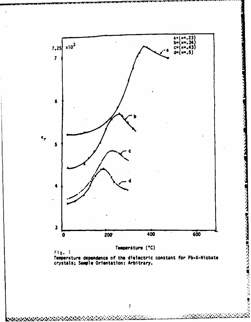
constant, fr. is shown in Figure 1. Here we observe that as x increases in Pbl-K 2.Nb 2O 6
samples. so does the ferroelectric Curie point and the magnitude of the transition. In
Figure 2. the compositional dependence of the Curie point (T,) and dielectric constant
at room temperature and at the transition point are presented. In Table III the absolute
values of T, and F, for each composition is given.
Table III
T, and f, of Pbi-K 2 Nb 2 O6 Crystals
Nominal x in Formula Curie c, at Er at c.Tc/fr. 25Crvsta] Point. °( 25°C T,
- --T ".8Ko.4.Yb206 478 1250 10.000 8.000.23 Pbo.77Ko.46Nb2O 6 367 .5208 7184 1.380.34 Pbo.66Ko.68 Nb2 O6 258 4433 .5653 1.280.43 Pbo.57 Ko.s 6Nb20 6 228 3713 4808 1.290.50 ___Pb_5_u K.Vb 0 18 5 3397 4392 1.29Notes
" . measured parallel to the longitudinal growth axis at IKHz.
XT' = constant for x = 0.23 - 0.50
A thorough dielectric characterization of PKN with x=0.2 has been done from room
temperature to about 600'C and in the frequency range from 100Hz to 100KHz 10.
Results and interpretations of this study will be presented separately at a later date. In
plhotographs I & 11 the samples of PKN are shown.
11.2 KTN. KTal zNbO:j
The K TN is one of the most interesting members of the ferroeleciric solid solution
steinis. It is perhaps the only truly solid solution ferroelectric. The end members of this
!ysteiu. KNbO3 (T, -x 70SK ) and KTaO3 (T, - 13K). are completely soluble in each other
.ielding ferroelectric solid solutions of anl desired composition of the type KTal-,N,()3
6Jq
a- (M-.23)
3b-m,-34)7.25 x10 c-(XI43
/ dm(K..5)7
6
CrS
4 d
~0 200 400 60
Temperature (OC)Fig. 1Temperature dependence of the dielectric constant for Pb-K-Niobatecrystals; Sample Orientation: Arbitrary.
7

8S r at T"
b e - :r at amwb.T
co e T C7
a 6600
T 9C CxI03CrlO
400 4
300 b 3
200 2
100
0 _
0 o2 3 4 .5 .6 . 7
x of crystal
I
Fig. 2 Dependence of the Curie point (Te) and dielectric constant (er) onEhe composition (x) for Pb-K-Niobae crystals
8

pp
Pb-K-Niobate Single Crystals
I. Pb-K-Niobate Single Crystals, Values of xcorrespond to the charge composition.
9

II. Pb-K-Niobate crystal with x - 0.4 (charge)
10

where x = 0 to 1. The compositional dependence of the ferroelectric Curie point is almost
linear [11] and it is extremely sensitive to Ta/Nb ratio. The T, increases with the increase
of Nb and it decreases when the Ta content in the solid solution is decreased. Like KNbO3
and KTaO3 all compositions in the KTal-.,NbO 3 synthesize in perovskite structure, i.e.
they can be represented by ABO.
The KTN crystals are extremely important both for fundamental research and novel
device applications. Samples having very low temperature Curie points are being studied
for quantum field effects whereas those samples which have the Curie points close to room
temperature are appropriate for a large number of applications in the fields of radiation
detection, electro-optics, signal processing etc.
Solid solutions of KTa _2 Nb.O 3 with x=0.35 have a large dielectric constant (e, > 104)
and. therefore. a very large electro-optic effect at room temperature. The nature of this
effect is quadratic (Kerr effect) in KTN. An extremely large effective linear electro-optic
effect (> 100 times that in materials like ADP and KDP) can be achieved by applying a
transverse field.
KTN shows high saturation polarization and very low dielectric losses. Therefore, it
is an attractive material for the following applications: 1. electro-optic and acousto-optic
light modulators and deflectors; 2. second harmonic generation; 3. parametric oscillators-
4. variable delay lines; 5. holographic data storage; 6. pyroelectric detectors and 7.
photorefractive devices.
Since its discovery [11,12) various efforts were made for the synthesis of KTN single
crystal using techniques such as Kyropoulos. Pfann, TSSG and ACRT. All these efforts
failed to produce optical quality KTN crystals. The crystals invariably possessed observ-
able si riatiois which are detrimental for the fabrication of efficient electro-optical devices.
Here the challenge is to synthesize optically transparent, striations free large single crys-
lals having no compositional gradient. Moreover, the ferroelectric Curie point should be
around rooni temperature (i.e. 25-35°C) so that the maximum value of the dielectric con-
slant. which is available in ferroelectrics at the Curie point, can be utilized. In general.
the higher the value of the dielectric constant, the higher is the electro-optical coefficient
as well as the amplification factor of a radiation detector.
11

The charge compositions for the crystal growth experiments were based on the fol-
lowing two factors: 1. the method of growth and 2. the desired crystal composition. Both
these parameters are dictated by the well established phase diagram of the KNbO3 -KTaO 3
system [11]. By adopting the usual practice of charge preparation-appropriate mass ratio
of K2CO 3:Nb 2 O5 :Ta2 Os, grinding, solid state reaction. sintering etc.-initially the crystals
of various compositions were grown by the methods like HTSG, ACRT. slow cooling etc.
All these crystals exhibited compositional gradient as well as colors ranging from black,
blue to green. These colors are caused by the reduction of pentavalent Nb and Ta. In
subsequent experiments these colors could be eliminated by adding a small amount (< 17(
by weight) of SnO 2 in the charge. The crystals grown by the mass transport method at
a constant temperature show no compositional gradients and only a few striations. They
are amber colored and usually they are 2 cm x 1 cm x 0.5 cm. The principle of this growth
technique can be outlined as follows: first of all the charge containing excess of K20 is
melted and then held at a temperature about 50 to 100'C higher than its melting point for
several hours to achieve complete homogeneity of the melt. Also, a positive 0 2 -pressure
of 6 to 10 psi was maintained in the growth chamber to prevent the loss of charge com-
position due to evaporation. The next step was to reduce the temperature of the melt
slowly so that crystallization took place in the bottom of the platinum crucible. Naturally.
for this to occur one must introduce a small temperature gradient between the bottom
and the top of the melt. Once a good size crystal was precipitated in the bottom of the
crucible, the temperature was raised to that temperature which would allow, according
to the phase diagram, the crystallization of a desired composition isothermally. At this
stage, an oriented seed is introduced and the crystal is allowed to grow. The inital crystal
precipitated at the bottom of the crucible acts as the nutrient material for the growth of
the oriented crystal with one unique composition. A good size crystal is grown in about
three to four days.
By this method we have been able to synthesize excellent crystals of three different
compositions of KTN, i.e. with x=0.66, 0.77 and 0.95 in the KTaj -NbO 3 series. The
temperature dependence of relative dielectric constant is shown in Figure 3. Here we
observe two things: 1. at the respective Curie points the values of tlhe dielectric constant
12
0 0 of 4e ... .- . ll % . . I , . - I % . .. . ....

is very high in these crystals, their range is between 10,700 to 14,457; and 2. the Curie point
increases as x in charge increases. In this figure, the values of x represent the original charge
compositions. The important parameters for our KTN crystals are presented in Table IV.
Photograph III shows one of our KTN crystals.
Table IV
Some Ferroelectric Properties of KTN Crystals
Growth Charge Crystal Curie Point, C,.,',b f,',T,
Temperature Composition Composition Tc[Kj[C (estimated)
1211 x=0.6 x=0.95 198 1.586 14,4571185 x=0.7 x=0.77 249 4.153 10.7001165 x=0.725 x=0.66 328 5,916 14,100
11.3 K-doped Pb-niobate, Pb3Nb 4013
This is one of the members of the PbO.Nb 20 5 series [13]. Its stoichiometric compo-
sition can also be expressed as 3PbO.2Nb 2O5 . Though it has been known to exist for a
long time, this composition was neither synthesized previously in single crystals nor ferro-
electricity was found in this material. During the search of suitable thermal conditions for
the growth of PKN with x = 0.2 using the self fluxing technique. we could synthesize the
single crystals of Pb 3 Nb 4 Ol 3 -. When the initial charge has the following compositions, this
material precipitates in single crystals both by static and dynamic slow cooling techniques:
PbO : Nb2 05 1.5 :1 by mole
K 2 CO 3 : Nb 205 1.5 : 1 by mole
That is.
PbO : K 2CO 3 : Nb 2O5 46.57:7.21:46.22 by weight.
The melting point of this material is about 1235°C and it solidifies at approximately
1220'( ' . When slow cooling is done at the rate of 1-2°Chi-' , single crystals synthesize by
spontaneous nucleation.
The crystals can be recovered by dissolving the flux in dilute HNO 3 . The crystals are
transparent and yellow, but they are rarely larger than 0.5 x 0.5 x 0.5 cm 3 in size. However.
13
- **%

15000'
14000-
12000-
11000 • XO.7£ XM.72=
10000
9000
p 000
7000-6000
4000
6M
2000
1000
0'0 50 100 150 200 290 300 350 40 40
Temperature (K]
Fig. 3 Dielectric Constant (6 r ) vs Temperature of KTaI.xNbxO3
14

*CM
III. K-Ta-niobate, KTa Ix Nb xO03 ' crystal
15

both quality and the size show a remarkable improvement when the accelerated crucible
rotation technique (ACRT) is employed in the growth process. In our experiments, the
maxinmum rotation rate of 22 rmp and the period (for ACRT) of 3 minutes were found to
be most effective. One of the ACRT grown Pb3 Nb4O 3 crystals is shown in the photograph
IV.
In the phase diagram of PbO.Nb2 Os 1131 one finds the 3PbO.2Nb 2O5 phase, which is
pyrochlore in structure, to coexist in a wide range with other phases. But it precipitates as
the single phase when the charge composition given above is used for the crystal growth.
So far as ferroelectricity is concerned in the PbO.Nb 2O5 system, only lead metaniobate
(PbNb 2 0O6 ) and PbNb 4O11 are found to be ferroelectric, whereas antiferroelectricity is
present in Pb-pyroniobate. Pb 2 Nb2OT. But in the single crystalline sample of Pb3Nb 4 O]3
we have found conclusive proof of the existence of ferroelectricity. The results are now
discussed here.
Figures 4 and , present the thermal behavior of dielectric constant (Er) and a.c.
conductivity (a) of this material. The existence of two Curie points-first at 10C and
the other at 393°('-is exremely important. The presence of the lower Curie point is
confirmed also by the a vs temperature measurement. However, the higher transition
point is not detected in the conductivity measurement. Nevertheless, the existence of
ferroelectricitv in this material is certainly important so far as the basic understanding of
the phenomenon is concerned. As reported in reference 14., the structure of this compound
is fcc with a, = 10.561A. This structure does not allow non-cenlro-syinmetrv which is a
necessary condition for the occurrence of ferroelectricity. A thorough investigation of
the determination of its structure has been undertaken (Prof. A. (learfield. Chinemistry
Department. Texas A&M University). We have found the existence of superlattice which
would allow the structure to be asymmetric. The investigations are being carried out
presently and a complete understanding of the structure will be available in a month or
Iwo. Then only we will be able to understand the origin of ferroelectricity in Pb 3 N)4) 13.
It is believed that K-' is responsible for superlattice. In our previous work on x-ray
diffraction 14. the presence of K-ion in this material could not be delected. Subsequently.
we could detect K inI Pb.3 Nb 4O,1 3 crystal by using EDAX analysis. However, we have not
16

IV. Pb-niobate, Pb3 Nb40 13 doped with K, crystal
17
S
" € o " W • " , ,'" ,(' q-' W'-', ,", 4' , " , WR • ' ,, °, -• ",

275 2746K (0100
250
225
200 660"K
(=393*C)
175
150
100 250 400 S~o700 860
T*KFig. 4 DIELECTRIC CONSTANT VS.
TEMPERATURE OF LEADNIOBATE, Pb3Nb4O13
18

4
3
5
it
270*K (a.30C)
31-
0 2103*6
Fig. 5 ELECTRICAL CONDUCTIVITYVS. TE14PEPATURE OF LEAD-NIOBATE, Pb 3Nb 401 3
19

yet determined its amount. But it is believed that the crystal is uniformly doped with K~'
This material appears to be an important material for further research. Its crystal quality,
transparency and high dielectric constant could make it suitable for some applications. The
steep rise in the conductivity at higher temperatures as shown in Fig. 5, leads one to believe
that the onset of extrinsic semiconduction effect is perhaps responsible for overriding the
ferroelectric effect in ar vs temperature behavior. In Table 4, we present the comparison of
Pb-niobates with respect to structure and ferroelectricity.
Table V
Structure and Ferroelectricity of Pb-niobates
COMPOND STRUCTURE NATURE TRANSITION POINTC
1. PbNb 20 6 Orthorhombic, Tungsten Metastable 560Bronze
2. PbNb 4O11 Orthorhombic or Tetragonal Ferroelectric 660
3. Pb 2 Nb 2 O 7 Rhombohedral, Pyrochlore Antiferroelectric -259
4. Pb3 Nb 4O 3 Pyrochlore Structure Ferroelectric -1 and 393FCC; ao=10.561AEvidence of superlatticeand K 'doping
III. SUMMARY
Important ferroelectric crystals like PKN and KTN can be grown to satisfy the re-
quirements of device engineering. Pb-K-niobate crystals are very difficult to grow without
multiple cracks in the boules. Here it has been shown how this serious problem can be
prevented by adopting some new techniques for the crystal growth. We have not only
sticceeded in the synthesis of the well known PKN crystal of the type Pb 0 .8 K0 4Nb 2 0
rather we have also found four new ferroelectric members of the Pb 1 -,K 2,Nb 2 O' family:
i.e. single crystals with x = 0.23. 0.34. 0.43 and 0.50. All these samples have fairly high
values of dielectric constants. Temperature and composition dependence of some impor-
tant properties have also been studied for all these crystals of PKN. The best quality single
crystals of KTN have been synthesized using the isothermal mass transport technique and
20

by maintaining a positive 0 2-pressure in the growth chamber. Three different composi-
tions of KTN crystals have been grown by this method. Their ferroelectric properties are
also discussed in this report. This research is in progress in our laboratory and we are
investigating the possibilities of: 1. growing optical quality PKN with no compositional
gradient: and 2. synthesizing KTN crystal with the Curie point at 25°C. Besides PKN
and KTN some amount of work was also done in growing single crystals of Pb-niobate
pyrochlore of the type. Pb 3 Nb 4 03. By using self-fluxing charge single crystals of this ma-
terial was grown by high temperature solution growth (HTSG) method. The best results
were obtained using the ACRT (accelerated crucible rotation technique). When doped
with K + ' this material exhibits ferroelectricity and it is believed that the formation of
superlattice in the pyrochlore structure introduces asymmetricity in the lattice which in
turn causes ferroelectricity in this material.
Acknowledgments: Even though AFOSR's support ended some time back for this
program, we have continued this research. As presented here, one can observe that sound
results are now available on PKN, KTN and Pb-niobate. We sincerely thank AFOSR,
and also ('aptai Kevin J. Mallov. for supporting this interesting research program. Our
thanks also go o Dr. R.('. Pohanka and Dr. Richard Brandt, Office of Naval Research.
for 1lheir interest and support to wur ferroelectric research efforts.
IV. REFERENCES
1. H.J. Scheel and P. Cuenter. ('rvstal (rowth of Electronic Materials. Editor E. Kaldis.(Chapter 12, pp. 149-157, (19.50. North-Holland. Amsterdam. New York.
2. R.W. Whatmore. J. Crystal Growth, 4S, (1980). pp. .530-5-17.
3. T. Yamada, J. Appl. Phys., 46, 7. (1975). pp 2361-2365.
4. H. Yamauchi. Appl. Phys. Lett., 32. 10. (19"s). pp. 599-600.
-5. T. Yamada. Appl. Phys. Lett., 23.5. (19731. p. 213-214.
6. W.F. Regnianlt. Research Report. Electrical Enineering Department. Penn St. Univ..(1977).
7. W.E. Kramer and (.W. Roland. J. Cryst. Growth, ',S. (1973). pp. 393-39 .
S. R.K. Pandev and U.Sridhar. Ferroelectrics, "." (1S3). pp. 21-27.
21

9. R.K. PandeNv and F. Islam. Paper No. 12A-2. IEEE/ISAF (IEEE International Sym-posium on Applications of Ferroelectrics, June 1986). Bethlehem. PA.
10. R.K. Pandey and A. Hossain. Paper No. T4.9. Proceedings of 1986 Fah Meeting ofMaterials Research Society, (December 1986). Boston, MA.
11. S. Triebwasser. Phys. Rev., 114, (1959). p. 63.
12. S. Triebwasser. U.S. Patent No. 2.954.300 September 27. 1960.
13. R.S. Roth. J. Research NBS. 6 1. (1959). p. 27-3s.
14. R.K. Pandev. K.W. Goeking, U. Sridhar. Charlotte Lowe-Ma, Paper No. PF-4. IEEEInternational Symposium on Applications of Ferroelectrics (ISAF). June 1986. Beth-leheni. PA.
22

DTI