iii. digital design & applications
TRANSCRIPT

163
III. Digital
Design &
Applications

164
3. Digital Design and
Applications
• 3.1 Introduction to Digital System
Design
• 3.2 Register-Transfer Level
• 3.3 Impediments to Synchronous
Design
• 3.4 Variable Entered Maps
• 3.5 Design steps for a digital
system
• 3.6 Digital Design Example

165
3.1.1 Problems for classical
Sequential Design
• Classical sequential circuit design
techniques could, in theory, be used in
arbitrarily complex design problems.
• In practice, however, classical
techniques are ineffective for all but
the simplest problems.
• Reason:
• The complexity of the design problem
overwhelms the human designer‘s ability
to find a correct solution
• Using classical techniques leads to
designs that are
• Hard to understand, hard to modify, and hard
to test

166
3.1.2 Software solutions to
Digital System Design
• Advantages:
• No need to design
hardware
• Software is relatively
easy to
change/customize
• Complex features can
be readily provided in
software
• Can test software
designs using
emulators.
• Disadvantages
• Microprocessors can be overly complicated for many controller problems
• Custom hardware can provide better performance than general-purpose hardware
• Custom techniques are still required in custom or semi custom integrated circuits
• Custom designs can be protected using patent or IC mask laws
•Many digital design problems are entirely
solvable using custom software and standard
microprocessor: examples ?

167
3.1.3 Basic Strategies in
Digital System Design• Top-down design
• Manage design complexity.
• Postpone commitment to any particular hardware
• Use iterative refinement to gradually converge on a natural solution
• Decompose a module into loosely interacting sub modules
• Design using high-level building blocks
• Conservative/safe design techniques
• Use synchronous hardware wherever possible
• Convert asynchronous inputs to synchronous inputs
• Use a robust system-wide clocking strategy
• Make design static if possible(ie. Correct operation is independent of clock speed)

168
3.1.3 Basic Strategies in
Digital System Design
(cont‘d)
• Conservative/safe design techniques
• Provide a single stepping mode
• Make design testable by construction
• Avoid obscure design tricks
• Document the design thoroughly
• Requirement, (user-oriented),
specification (designer-oriented)
• Reasons for designs decisions
• List relevant standards
• Propose test plans
• Develop maintenance procedures
• Consider manufacturability issues

169
3.1.4 Signals at External
Interface
• System level control signals:
• Highest level commands
• External user is shielded form internal details
• System level status signals
• Simplified high-level status information is provided to the external user
• Data in
• Analog signals are typical converted to digital processing
• Data out
• Analog signals may need to be reconstructed from their internal digital representation
Digitalsystem
control signal
statussignal
data in
data out

170
3.1.5 Highest Level of System
Architecture
• Control path
• Circuit that control
algorithm by which
operators are
applied to the data
• State control and
data operation
sequencing are
emphasized
• Typical control
units:
• Registers
• Next state logic
• Output logic
• Control+status line
• Data path
• Circuits that
directly store and
transform the data
• Bit parallelism and
regular structure
are emphasized
• Typical data path
elements:
• Registers
• Multiplexes
• Shift/adders/ALUs
• Counters
• buses

171
3.1.5 Highest Level of System
Architecture (cont‘d)
controller
data in
internalcontrolsignal
data path
data out
externalcontrolsignal
internalstatussignal
externalstatussignal

172
3.2 Register Transfer Level
• A convenient conceptual level intermediate between the system level and the gate level
• RTL assumes a set of hardware constructs are defined in FPGA hardware and library elements
• HDL code is mapped to these constructs
• Describe the operation of synchronous system
• Combine the control-flow state machine with means for defining and operating multi-bit registers
• Typical RTL constructs:
• Combinational logic
• Arbitrary functions (random logic, ROMs, PALs, PLAs)
• Multiplexers
• Demultiplexers/decoders
• Comparators
• Arithmetic./logic circuits (ALUs, adders, subtractors)

173
3.2 Register Transfer Level
(cont‘d)
• Sequential Logic
• Latches, flip-flops
• Registers, shift registers
• Counters, LFSRs
• RAMs
• Interconnect:
• Buses
• Wires
• Buffers
• Tri-state able buffers
• Bi-directional transceivers

174
3.2.1 Multiplexers (Mux)
• Multiplexer is a digital switch
• It connects data from one of n sources to
its output.
• A logic equation:
• Summation symbol represents a logical
sum of product terms
• iY is a particular output bit (1 <= i< =b)
• iDj is input bit I of source j (0<=j<=n-1)
• Mj represents minterm j of the s select
inputs
• ? The relationship between S and n
1
0
n
j j
j
iY EN M iD
data out
Enable
selects
b
b
b
n datasource
EN
SEL
D0
D1
Dn-1
b
Multiplexer

175
3.2.1 Multiplexers (cont‘d)
• Example 4 to 1 MUX
• How to implement?
4 X 1
MUX
Io
S1
I1
I2
I3
EN
S0
Y EN S1 S0 Y
1 x x 0
0 0 0 I0
0 0 1 I1
0 1 0 I2
0 1 1 I3
176
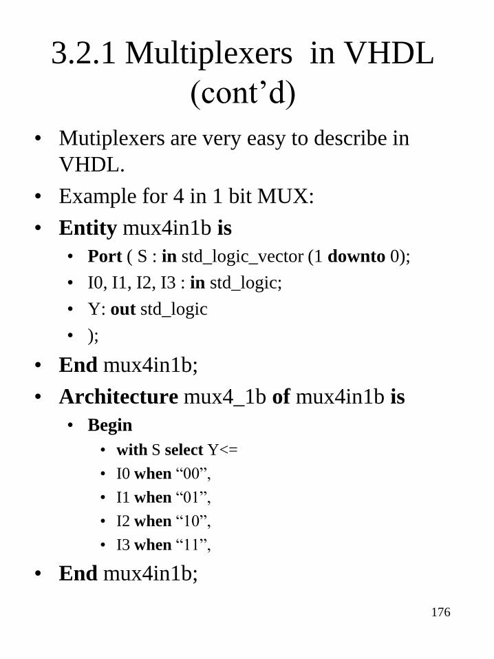
3.2.1 Multiplexers in VHDL
(cont‘d)
• Mutiplexers are very easy to describe in
VHDL.
• Example for 4 in 1 bit MUX:
• Entity mux4in1b is
• Port ( S : in std_logic_vector (1 downto 0);
• I0, I1, I2, I3 : in std_logic;
• Y: out std_logic
• );
• End mux4in1b;
• Architecture mux4_1b of mux4in1b is
• Begin
• with S select Y<=
• I0 when ―00‖,
• I1 when ―01‖,
• I2 when ―10‖,
• I3 when ―11‖,
• End mux4in1b;

177
3.2.1 Expanding Multiplexers
• Expand 4 input 1 bit output multiplexer to 4 input 8 bit output multiplexer
• Entity mux4in8b is
• Port ( S : in std_logic_vector (1 downto 0);
• I0, I1, I2, I3 : in std_logic_vector (1 to 8) ;
• Y: out std_logic_vector (1 to 8)
• );
• End mux4in8b;
• Architecture mux4in_8b of mux4in8b is
• Begin
• with S select Y<=
• I0 when ―00‖,
• I1 when ―01‖,
• I2 when ―10‖,
• I3 when ―11‖,
• End mux4in_8b;

178
3.2.1 Expanding Multiplexers
(cont‘d)
• Expand 4 input 1 bit output
multiplexer to 8 input 1 bit output
multiplexer
• How to implement it in VHDL?
4 X 1
MUX
Io
S1
I1
I2
I3
EN
S0
Y
4 X 1
MUX
Io
S1
I1
I2
I3
EN
S0
Y

179
3.2.2 DeMultiplexers
• Used to direct data to one of two or
more possible destinations
data in
Enable
selects b
b
b
data out
EN
SEL Y0
Y1
Yn-1
b
DeMultiplexer
DE
MUX
Y0
S1
Y1
Y2
Y3
E
S0
S1 S0 Y0 Y1 Y2 Y3
0 0 E 1 1 1
0 1 1 E 1 1
1 0 1 1 E 1
1 1 1 1 1 E

180
3.2.2 DeMultiplexers in
VHDL
• Example for demux:
• Entity Demux is
• Port ( S : in std_logic_vector (1 downto 0);
• E : in std_logic;
• Y0, Y1, Y2, Y3: out std_logic
• );
• End Demux;
• Architecture Demux of demux is
• Begin
case S is
When ―00‖ =>
Y0<=E ;
When ―01‖ =>
Y1<=E ;
When ―10‖ =>
Y2<=E ;
When ―11‖ =>
Y3<=E ;
End case ;
• End demux;

181
3.2.3 Comparators
• Comparing two binary words for
equality
A BA=B?
4 4
1
A0 B0 A1 B1 A2 B2 A3 B3
A=B
PI
CI module Co
Po
PI
CI module Co
Po
PI
CI module Co
Po
PI0 PI1 PIn-1
Po0 Po1 Pon-1
C0 C1 C2Cn-1
Cn
cascading
input
cascading
output
182
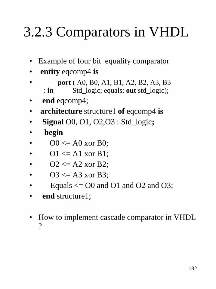
3.2.3 Comparators in VHDL
• Example of four bit equality comparator
• entity eqcomp4 is
• port ( A0, B0, A1, B1, A2, B2, A3, B3 : in Std_logic; equals: out std_logic);
• end eqcomp4;
• architecture structure1 of eqcomp4 is
• Signal O0, O1, O2,O3 : Std_logic;
• begin
• O0 <= A0 xor B0;
• O1 <= A1 xor B1;
• O2 <= A2 xor B2;
• O3 <= A3 xor B3;
• Equals <= O0 and O1 and O2 and O3;
• end structure1;
• How to implement cascade comparator in VHDL ?

183
3.2.4 Binary Adders
• Half adders: adds two 1 bit operands X and
Y, producing a 2-bit sum. The lower-order
bit of the sum may be named HS (half sum),
and the higher-order bit may be named CO
(carry out)
• HS= X xor Y=XY‘+X‘Y
• CO=XY
• Full adders: to add operands with more than
one bit, we must provide for carries between
bit positions. The building block for this
operation called full adder.
• Besides the added-bit inputs X and Y, a full
adder has a carry-bit input, Cin.
• Out put is named S (sum) and Cout (carry
out)
• S= X xor Y xor Cin
• Cout=XY+XCin+YCin

184
3.2.4 Binary Adders (cont‘d)
(a) One possible circuit that performs the
full adder equations
(b) The corresponding logic symbol
(c ) symbol for cascaded full adders
X YCout Cin
S
X
Y
Cin
S
Cout
full adder
Y S
Cout
(a)
(b)
(c)
X
Cin
1 1
11
1

185
• Entity for a full adder
• entity adder is
• port ( X, Y, Cin : in Std_logic;
• S, Cout : out Std_logic);
• end adder;
• Ripple adder : two binary words, each
with n bits, can be added using a ripple
adder– cascade of n full-adder stages,
each of which handles one bit.
• Ripple adder is slow, why ?
• Some other adders ?
X YCout Cin
S
S3
C4
X3 Y3
X YCout Cin
S
S2
C3
X2 Y2
X YCout Cin
S
C2
X1 Y1
X YCout Cin
S
C1
X0 Y0
C0
S1 S0
3.2.4 Binary Adders (cont‘d)

186
3.2.4 Binary Adders in VHDL• entity rippleadder is
• port ( X, Y: in Std_logic_vector(0 to 3);
• S : out std_logic_vector( 0 to 3);
• Cout : out Std_logic);
• end rippleadder;
Architecture structure1 of rippleadder is
component adder –pre-defined part type
port ( X, Y, Cin : in Std_logic;
• S, Cout : out Std_logic);
End component;
Signal Cout0cin1, cout1cin2, cout2cin3 : in std_logic;
Begin
adder_0: adder port map (X=>X(0), Y=>Y(0),Cin =>low, S=> s(0), Cout => Cout0cin1);
adder_1: adder port map (X=>X(1), Y=>Y(1),Cin =>Cout0cin1, S=> s(1), Cout => Cout1cin2);
adder_1: adder port map (X=>X(0), Y=>Y(0),Cin =>Cout1cin2, S=> s(2), Cout => Cout2cin3);
adder_1: adder port map (X=>X(0), Y=>Y(0),Cin =>Cout2cin3, S=> s(3), Cout => Cout);
End structure1 ;
X YCout Cin
S
S3
C4
X3 Y3
X YCout Cin
S
S2
C3
X2 Y2
X YCout Cin
S
C2
X1 Y1
X YCout Cin
S
C1
X0 Y0
C0
S1 S0

187
3.2.4 A Design Example:
Recursive Adder/Subtractor
• Objective: Implement an adder and
subtractor using VHDL.
• Design steps
• Define Specifications
• Data Path Design
• Control Path Design
• Simulation
• Hardware Implementation
• Testing

188
3.2.4 Define Specifications
• 4-bit Switch Input A
• 4-bit Switch Input B
• 1 bit switch for Opcode.
• LED output 4 LED for Sum, one for
• Cout, one done signal
• Restricted building blocks:
• An inverter, 2 2N-N mux, three registers
and an adderN.
A B
Sum Cout
OPcode
4 4
4
Done

189
3.2.4 Define Specifications
• Opcode 0, A+B
• example 0101+0111
• Opcode 1, A-B=A+NotB+1
• Example 1100-0011=?
• Adder implementation
• Ripple adder
• fast adder
• Register ? Synchronize the add and
subtract procedure
Q3 Q2 Q1 Q0
D3 D2 D1 D0
ClockLoad
Clear

190
3.2.4 Example : Data Path

191
3.2.4 Example : Data Path
Entity
• Entity DataPath is
• port ( A, B in Std_logic_vector(3 downto 0);
• loadA, loadB : in std_logic;
• CK, reset1 ,sw : in std_logic;
• Sum : out std_logic_vector(3 downto 0);
• Cout : out std_logic );
• end Entity DataPath;
• Architecture struture1 of DataPath is
• Signal NotB : std_logic_vector(3 downto 0);
• Signal OutMuxB : std_logic_vector(3 downto 0);
• Signal InternalA, InternalB : std_logic_vector(3 downto 0);
• Signal inC: std_logic;
• Begin
• …
• End architecture structure1;

192
3.2.4 Example : Control Path
• Control Signals in Data Path
• Sw Control the mode
• Reset, reset the output active low
• CK, clock synchronize the calculation
of Sum and sub
• Load A, Load B: allow the input of
register to be loaded into the register.
• Done : High when the calculation is
done, low when the reset is activated.

193
3.2.4 Example : Control Path

194
3.2.4 Example : Final Design
Controller
A
Data Path
Sum
B SW
Cout
enter reset
clk
done
reset1
loadA
loadB
4 4

195
3.2.4 Hardware
Implementation
• Wiring
• Pin assignment
• Programming
• Testing

196
3.2.5 Shift Register
• A shift Register is an n-bit register
with a provision for shifting its stored
data by one bit position at each tick of
the clock. Following is a 4-bit register:
Q3 Q2 Q1 Q0
D3 D2 D1 D0
ClockLoad
Clear
Q
Clk Clr
D
Q
Clk Clr
D
Q
Clk Clr
D
Q
Clk Clr
D
MUX2 to1
I0 I1
S0MUX2 to1
I0 I1
S0MUX2 to1
I0 I1
S0MUX2 to1
I0 I1
S0
clock
clear
Load D3 D2 D1D0
Q3 Q2 Q1 Q0

197
3.2.5 Shift Register (cont‘d)
• Multi-mode 4 bit shift register
Q3 Q2 Q1 Q0
P3 P2 P1 P0
Clock mode (S1S0)Clear
L.S.I
2
R.S.I
S1 S0 Mode
0 0 Hold
0 1 Load
1 0 Shift left
1 1 shift right
Q
Clk Clr
D
Q
Clk Clr
D
Q
Clk Clr
D
Q
Clk Clr
D
MUX4 to1
I0 I1 I2 I3
SMUX4 to1
I0 I1 I2 I3
SMUX4 to1
I0 I1 I2 I3
SMUX4 to1
I0 I1 I2 I3
S
clock
clear
Mode
Q3 Q2 Q1 Q0
2
P3 P2P1
P0L.S.I R.S.I

198
3.2.5 Shift Register in VHDL• Entity Vshftreg is
• Port(
• Clk, clr,rin,lin : in std_logic;
• S: in std_logic_vector (2 downto 0); --function select
• D: in std_logic_vector(7 downto 0); --data in
• Q: out std_logic_vector (7 downto 0) –data out
• );
• End entity;
• Architecture vshftreg_arch of vshreg is
• Signal Iq: std_logic_vector ( 7 downto 0);
• Begin
• Process(clk,clr,iq)
• begin
• If(clr=‗1‘) then Iq <= (others=>‘0‘);--asynchronous clear
• Elsif (clk‘event and clk=‗1‘) then
• Case conv_integer(s) is
• When 0 => null; --hold
• When 1=> iq <=D; --load
• When 2 =>iq <=rin & iq( 7 downto 1); --shift right
• When 3 => iq <= iq( 6 downto 0) & lin; --shift left
• When 4=> iq <=iq(0) & iq( 7 downto 1); --circular right
• When 5 => iq <= iq( 6 downto 0) & Iq(7); --circular left
• When 6 => iq <=iq(7) & iq(7 downto 1); --shift arith right
• When 7 => iq <=iq( 6 downto 0) & ‗0‘; --shift arith left
• When others => null;
• End case;
• End if;
• Q<=iq;
• End process;
• End vshftreg_arch;

199
3.2.6 Counters
• Counter is generally used for any a
clocked sequential circuit whose state
diagram contains a single cycle.
• The modulus of a counter is the number
of states in the cycle
• Counter with m states is called a modulo-
m counter of a divide-by-m counter
S1S2
S3
S4S5
Sm
Q Q'
CLK D
Q Q'
T
Use D flip flop to
construct a T Flip flop

200
3.2.6 Counters (cont‘d)
• Ripple counters : can be constructed
with just n flips –flops and no other
components—drawback slow
• Synchronous counters: connect the
inputs to the same common Clk signal.
• Clock period should > propagation
delay.—improvement: synch parallel
counter
Q Q'
T
Q0
Q Q'
T
Q1
Q Q'
T
Q2
Q Q'
T
Q3
Clk
Q Q'
EN T
Q0
Q Q'
T
Q1
Q Q'
T
Q2
Q Q'
T
Q3
Clk
CNTEN

201
3.2.6 Counters (cont‘d)
• LFSR: linear Feedback shift register
counters.
• Many shift register counters have far less
than the maximum of 2n normal states ( n-
bit).
• LFSR can have 2n –1 states.
• LFSR is called maximum-length
sequence generator.
• Based on finite field theory Evariste
Galois (1811-1832)

202
3.2.7 Buses
• Bus is a collection of two or more
related signals lines. They are used to
move data around within a system and
among systems.
• Bus are drawn with a double or heavy line
• A slash and a number may indicate how
many individual signal lines are contained
in a bus
• Size may be denoted in the bus name (e.g.
inbus[31..0].
• Why we need a bus?
A
B C A B C

203
3.2.7 Buses (cont‘d)
• Direct connection
• Advantages:
• High bandwidth
• No sharing
required
• Disadvantages:
• Number of
wires increases
rapidly as each
new system is
added
• Bus connection
• Advantages:
• Less wiring
• Easy & cheap to add a new system
• Disadvantages:
• Bus becomes a bottle neck
• Need control circuitry to prevent bus contention

204
3.2.8 Three State Buffers
• Three state buffer or three state driver.
• Three states 0, 1 or Hi-Z
• Various three-state buffers
• A) non-inverting, active high enable
• B) non inverting, active-low enable
• C) inverting, active-high enable
• D) inverting, active-low enable
Bi-directional transceivers
A B
DIR
direction mode
L B to A
H A to B

205
3.2.9 RAM
• RAM: random access memories,
which means that the time it takes to
read or write a bit of memory is
independent of the bits location in the
RAM.
• SRAM (static RAM): once a word is
written at a location, it remains stored
as long as power is applied to the chip.
Unless what ?
• DRAM (dynamic RAM): the data
stored at each location must be
refreshed periodically by reading it
and then writing it back again. Why ?

206
3.2.9 RAM (cont‘d) : a
Simplified Block Diagram of
RAM
Memory Array
d
e
c
o
d
e
r
t ransceiver
a
d
d
r
e
s
s

207
3.3 Impediments to
Synchronous Design
• Synchronous approach is the most straightforward and reliable method of digital system design, however…
• Synchronous systems using edge-triggered flip-flops work properly only if all flip-flops see the triggering clock at the same time.
• Clock skew: the situation when the clock signal arrives at different flip-flops at different times
• Caused by unequal clock propagation times
• Clock skew may cause flip-flops to load transient input signals.

208
3.3.1 Clock Skew : Example
of Clock Skew
IN
Clock
QD D Q
delay
ClockD
Clock
IN
Q1
ClockD
Q2

209
3.3.1 Clock Skew (cont‘d)
• Clock skew are caused by
• Buffering method
• DC and AC loading
• Signals on PCB are auto routed by CAD
• Some wire maybe slower than other
• To control this problem, many high
performance systems and VLSI chips
use a two-phase latch design
ClockClock
Clock1
Clock2
Clock
Clock1
Clock2
Clock3

210
3.3.1 Two Phase Clocking
• Popular in custom CMOS ICs
• Standard scheme at IBM
• Advantages:
• Simple memory elements
• Essential hazards avoided
• Clock skew problems avoided
• Disadvantages
• Two separate clock signals are required
• Non-overlapping condition must be guaranteed to ensure correct operation
Comb.
Logic
Memory Comb.
LogicMemory
I
N
P
U
T
o
u
t
p
u
tClock1 Clock2
Clock1
Clock2

211
3.3.2 Gating the Clock
• If CLKEN is a state machine output or
other signal produced by a register
clocked by clock, the CLKEN changes
some time after clock has already gone
high. This produces glitches and false
clocking of the registers controlled by
GCLK
• AND gate delays gives GCLK excessive
clock skew, which cause problems.
Clock
GCLK
Clock
CLKENGCLK
CLKEN

212
3.3.2 Gating the Clock
(Cont‘d)
• An acceptable way to gate the clock
Clock
Before: GCLK
Clock
CLKENGCLK
CLKEN
GClk
CLKEN

213
3.3.3 Asynchronous Input
• There are always asynchronous inputs
• Key input (very low frequency)
• Interrupts
• Status flags
• Solution synchronizer:
Clock
Asyncin
Synchronous
System
Asyncin
Clock
D Q
Syncin

214
3.3.3 Asynchronous Input
(cont‘d)
• It is essential for asynchronous inputs
to be synchronized at only one place
Clock
Asyncin
Synchronous
System
Clock
D Q
Syncin1
Asyncin
D Q
Syncin2

215
3.4 Variable Entered Maps
(VEM)
• Regular K-maps
entries
• 1
• 0
• Don‘t care
• VEM entries
• 1
• 0
• Don‘t care
• Boolean variables
• expressions
• Add the power to K-map method
• Reduce the work to plot and read maps
• A technique to reduce the map size.
A B C F
0 0 0 0
0 0 1 0
0 1 0 1
0 1 1 1
1 0 0 1
1 0 1 0
1 1 0
1 1 1
0 1
0 0 c'
1 1
AB
00 01 11 10
0 0 1 1
1 0 1 0
ABC
A B C F F
0 0 0 0 0
0 0 1 0 0
0 1 0 1 c'
0 1 1 1 c
1 0 0 1 c'
1 0 1 0 0
1 1 0 c'o
1 1 1 co

216
3.4.1 Variable Entered Maps
(cont‘d)
• VEM are most effective when a
function depends strongly on <= 4
inputs and depends only weakly on the
remaining inputs.
• Map Entered variable (MEV) : a
variable that appears in a box in a
VEM
A B C F
0 0 0 f0
0 0 1 f1
0 1 0 f2
0 1 1 f3
1 0 0 f4
1 0 1 f5
1 1 0 f6
1 1 1 f7
0 1
0c'f0+cf1
c'f4+cf5
1c'f2+cf3
c'f6+cf7
AB00 01 11 10
0 f0 f2 f6 f4
1 f1 f3 f7 f5
ABC
A B C F
0 0c'f0+cf1
0 0
0 1c'f2+cf3
0 1
1 0c'f4+cf5
1 0
1 1c'f6+cf7
1 1
217
3.4.2 Plotting the Map
• How to plot a VEM from a truth table
• Select the MEV
• Partition the truth table so that the non-
MEVs have the same values in each
partition
0 1
0 c 1
1 c' 0
BA B C F1 F2 F3 F4
0 0 0 0 1 0 1
0 0 1 1 0 0 1
0 1 0 1 0 1 0
0 1 1 0 1 1 1
1 0 0 1 0 0 1
1 0 1 1 0 1 0
1 1 0 0 1 1 0
1 1 1 0 1 0
A 0 1
0 c' 0
1 c 1
BA
0 1
0 0 c
1 1 c'
BA 0 1
0 1 c'
1 c c
BA

218
3.4.2 Plotting the Map(cont‘d)
• How to plot a VEM from an equation
• Rearrange the function into S.O.P form
• Identify the most dependant variable
• Factor out the minterms in the identified
variables
• Draw out an map
• Fill in the VEM
• Example :

219
3.4.3 Reading Theory
• Step1: first image that all 1 entries in the map
are replaced by the map entered variables
Ored with its complement. 1=D+D‘
• First loop all single MEV entries that will not loop
with another identical MEV in an adjacent cell or
with a 1 or don‘t care (island).
• Loop all MEV‘s that will loop into duals only with
another identical MEV in an adjacent cell
• Loop all MEV‘s that will loop into a dual only
with a 1.
• Loop all MEV‘s that will loop into a dual only
with a don‘t care.
• Any MEV that will loop two ways with another
identical MEV, 1 or don‘t care but won‘t loop into
a quad, leave until later
• Continue looping in similar fasion for quads and
groups of eight until every MEV has been looped
at least once

220
3.4.3 Reading Theory (cont‘d)
• Step2: once all single MEV entries have been covered, transform the map according to the following transformations:
• A) Replace the MEV and MEV‘ with 0.
• B) 0 to 0, don‘t care to don‘t care
• C) 1 : two possible transformations:
• 1 if not completed covered
• Don‘t care if completed covered, I.e. looped with both the MEV and MEV‘
• Step3: OR together the terms from steps 1 and 2
) 0
) ( ) ( )
1 covcovcov
cov
D MEV and MEV
E MEV MEV and MEV MEV
if not ered at all or ifjust the is eredif completed ered orif just thenecessarytermis ered

221
3.4.3 Reading Theory (cont‘d)
D
D'
0
0
0 0
D 1
D'
0
0
D
D'
0
0
0 D+D'
D'
0 1
0
1 D+D'
D'
A)
B)
C)D 1
0
0 1
0
D)
E)

222
3.4.3 Reading Theory
(cont‘d): example1
0 1
0
1
C 0
1 C
given
step1
step2
AB
0 1
0
1
C 0
C+C' C
AB
0 1
0
1
C 0
C+C' C
AB
0 1
0
1
0 0
1 0
AB
F AC BC AB

223
3.4.3 Reading Theory
(cont‘d): example2
A B C D F1 F2
0 0 0 0 0
0 0 1 1 0
0 0 1 0 1 1
0 0 1 1 0 1
0 1 0 0 1 0
0 1 0 1 1 1
0 1 1 0 1
0 1 1 1 0 1
1 0 0 0 0 0
1 0 0 1 0 0
1 0 1 0 1
1 0 1 1 1 0
1 1 0 0 0 0
1 1 0 1 1
1 1 1 0 0 1
1 1 1 1 0
00 01 11 10
0
1
ABC
00 01 11 10
0
1
ABC
00 01 11 10
0
1
ABC
00 01 11 10
0
1
ABC
1
2
F BCD AD ABC
F ABD CD AC

224
3.5 Design Steps for Digital
System Design
1. Define the system specifications
2. Develop a rough design for the
system
3. Develop a detailed design for the
data path
4. Develop a detailed specification for
the controller
5. Complete the design of the controller
6. Finalize the design
7. Simulation and hardware
implementation

225
3.5.1 Step1:Define the System
Specifications
• Define the purpose of the system
• Input, output
• System-level
• Define the system‘s operation
• Algorithms
• flowchart
• Define the operational constrains
• Cost
• Speed
• Size
• Power requirement
• Reliability
• Upgrade ability
• Marketing plans
• Other considerations

226
3.5.2 Step2 : Develop a Rough
Design for the System
• Objectives
• Define the control relationships within
system
• Define basic sequential behavior
• Identify functional units in data path
• Choose signal names
• Graphical illustrations
• Block diagram
• flowchart

227
3.5.3 Step3: Develop a
Detailed Design for the
Data Path
• Objectives
• Fully define the data path
• Documentation aids
• Detailed timing diagram
• Detailed flowchart
• Detailed functional partial partition

228
3.5.4 Step4 : Develop a
Detailed Specification for the
Controller
• Objectives:
• Fully specify the controller behavior
• The operation of the system controller
is completed defined by the detailed
flowchart
• The controller is a synchronous
sequential machine
• It should be expressed as a state
diagram.
• Translate the flow diagram to a state
diagram
229
3.5.4 Step4 : Rules for
Converting Flow Chart to
State Diagram
• Rule1 : Action block in flow
diagram state in the state diagram
action1
action2
condition
Yes
No action1
action2
condition
condition

230
Example

231
3.5.4 Step4 : Rules for
Converting Flow Chart to
State Diagram(cont‘d)
• Rule2: the branching conditions for a
state are derived by tracing through all
possible decision paths from the given
action block to all possible other
action blocks
action1
action2
condition
Yes
No action1
action2
condition
condition

232
Example

233
3.5.4 Step4 : Rules for
Converting Flow Chart to
State Diagram(cont‘d)
• Rule3: Avoid making branching
decisions on more than one
asynchronous variable at a time
A
Data
Skip
term
B C
N
N
N
Y
Y
Y
A
B C
Data'+skip
Data.Skip'.term'
Data.Skip'.term

234
3.5.4 Step4 : Rules for
Converting Flow Chart to
State Diagram(cont‘d)
• Rule3: Avoid making branching
decisions on more than one
asynchronous variable at a time
A
Data
Skip
term
B C
N
N
N
Y
Y
D
B C
term'term
D
A
Data'+skip
Data.skip'

235
3.5.5 Step5: Complete the
Design of the Controller
• Complications:
• Short/brief input pulses
• Asynchronous inputs
• Avoid glitches in the outputs
• Debug and testability features
• Design steps:
• Select a controller architecture
• Deal with synchronous problems
• Select a clock frequency
• Find a suitable state assignment
• Use a state map
• Implement the next state maps
• Plot next state maps
• Design the output decoder
• Plot output maps (if necessary)
• Produce an output list

236
3.5.6 Step6 : Finalize the Design
Controller Data Path Interface
controller
data in
internalcontrolsignal
data path
data out
externalcontrolsignal
internalstatussignal
externalstatussignal

237
3.5.7 Step7: Simulation and
Hardware Implementation

238
3.6 An Example: pop machine
controller
• Requirement:
• Pop machine capable of automatically
dispensing soda pop at 75 cents per
can and make proper change for coin
sequences comprising nickels, dimes,
quarters. The new machine use
existing inventory including coin
receiver, coin changer, and pop drop
mechanism. These three given
subsystems are to be controlled by a
newly designed digital controller.

239
3.6.1 Specs• Constrains:
• Must operate out of doors
• Must operate in an electrically noisy environment
• Mean time between failures > 2 months
• Hardware constraints : coin receiver, coin changer and pop-drop mechanism have already been chosen.
pop-drop
popready
drop
changer
changeready
eject
receiver
manualcoin
release
coin drop
coin present
quarter
nickle
dime
clear (L)

240
3.6.1 Specs (cont‘d)
• Time Specs for the coin receiver
quarter
nickle
dime
coin present
• Time Specs for the coin changer
eject
change ready

241
3.6.2 Roughly Define System
Operation
pop-drop
CoinChanger
CoinReceiver
SystemController
Start
Coin
received
ACC
ACC >= 75
ACC= 75
Drop POPclear ACC
return nickle and
reduce ACC
N
N
NY
Y
Y

242
3.6.2 Roughly Block Diagram
for the Data Path
Combinationallogic
Adder
Coin receiver
Coin type
Coin value
Register
Comparator
75
A>B
A=B
A<B

243
3.6.3 Refined Data Path
Combinationallogic
Adder
Coin type
Coin value
Register
Comparator
75
A>B
A=B
A<B
Coin ReceiverClearDrop coincoin Present
counterLoadClearCount Down

244
3.6.4 Develop a detailed
specification for the controller
Start
Coin
present
a
coinpresent
b
c
ACC<75
ACC>75
d f
pop dropready
e
Clear ACC, drop pop
changeready
N
Y
Y
N
Y
N
N
N
N
fdec ACC by nickle

245
3.6.5 Complete the Design of
Controller
a
b
c
d
e
f
g
coin present
coin present
coin present
coin presentACC < 75
ACC > 75ACC = 75
change ready
change ready
pop drop ready
pop drop ready

246
3.6.6 Finalize the Design:
Controller Data Path Interface
Data PathControl
path
<75
=75
>75
clear ACC
DEC ACC
coinreceiver
coinchanger
pop drop
drop_pop
drop_ready
change_ready
return nickle
clear
coin present
drop coin
coin signal
coin present

247
3.6.7 VHDL Implementation

248
3.6.7 Digital Design
a
b
c
d
e
f
g
coin present
coin present
coin present
coin presentACC < 75
ACC > 75ACC = 75
change ready
change ready
pop drop ready
pop drop ready
00 01 11 10
0
1
ABC
00 01 11 10
0
1
ABC

249
3.6.7 Digital Design
00 01 11 10
0
1
ABC
00 01 11 10
0
1
ABC
00 01 11 10
0
1
ABC

250